US7192876B2 - Transistor with independent gate structures - Google Patents
Transistor with independent gate structuresDownload PDFInfo
- Publication number
- US7192876B2 US7192876B2US10/443,375US44337503AUS7192876B2US 7192876 B2US7192876 B2US 7192876B2US 44337503 AUS44337503 AUS 44337503AUS 7192876 B2US7192876 B2US 7192876B2
- Authority
- US
- United States
- Prior art keywords
- layer
- semiconductor structure
- over
- sidewall
- top surface
- Prior art date
- Legal status (The legal status is an assumption and is not a legal conclusion. Google has not performed a legal analysis and makes no representation as to the accuracy of the status listed.)
- Expired - Fee Related, expires
Links
Images


Classifications
- H—ELECTRICITY
- H10—SEMICONDUCTOR DEVICES; ELECTRIC SOLID-STATE DEVICES NOT OTHERWISE PROVIDED FOR
- H10D—INORGANIC ELECTRIC SEMICONDUCTOR DEVICES
- H10D30/00—Field-effect transistors [FET]
- H10D30/60—Insulated-gate field-effect transistors [IGFET]
- H10D30/62—Fin field-effect transistors [FinFET]
- H—ELECTRICITY
- H01—ELECTRIC ELEMENTS
- H01L—SEMICONDUCTOR DEVICES NOT COVERED BY CLASS H10
- H01L21/00—Processes or apparatus adapted for the manufacture or treatment of semiconductor or solid state devices or of parts thereof
- H01L21/02—Manufacture or treatment of semiconductor devices or of parts thereof
- H01L21/04—Manufacture or treatment of semiconductor devices or of parts thereof the devices having potential barriers, e.g. a PN junction, depletion layer or carrier concentration layer
- H01L21/18—Manufacture or treatment of semiconductor devices or of parts thereof the devices having potential barriers, e.g. a PN junction, depletion layer or carrier concentration layer the devices having semiconductor bodies comprising elements of Group IV of the Periodic Table or AIIIBV compounds with or without impurities, e.g. doping materials
- H—ELECTRICITY
- H10—SEMICONDUCTOR DEVICES; ELECTRIC SOLID-STATE DEVICES NOT OTHERWISE PROVIDED FOR
- H10B—ELECTRONIC MEMORY DEVICES
- H10B41/00—Electrically erasable-and-programmable ROM [EEPROM] devices comprising floating gates
- H10B41/30—Electrically erasable-and-programmable ROM [EEPROM] devices comprising floating gates characterised by the memory core region
- H—ELECTRICITY
- H10—SEMICONDUCTOR DEVICES; ELECTRIC SOLID-STATE DEVICES NOT OTHERWISE PROVIDED FOR
- H10B—ELECTRONIC MEMORY DEVICES
- H10B69/00—Erasable-and-programmable ROM [EPROM] devices not provided for in groups H10B41/00 - H10B63/00, e.g. ultraviolet erasable-and-programmable ROM [UVEPROM] devices
- H—ELECTRICITY
- H10—SEMICONDUCTOR DEVICES; ELECTRIC SOLID-STATE DEVICES NOT OTHERWISE PROVIDED FOR
- H10D—INORGANIC ELECTRIC SEMICONDUCTOR DEVICES
- H10D30/00—Field-effect transistors [FET]
- H10D30/01—Manufacture or treatment
- H10D30/021—Manufacture or treatment of FETs having insulated gates [IGFET]
- H10D30/024—Manufacture or treatment of FETs having insulated gates [IGFET] of fin field-effect transistors [FinFET]
- H—ELECTRICITY
- H10—SEMICONDUCTOR DEVICES; ELECTRIC SOLID-STATE DEVICES NOT OTHERWISE PROVIDED FOR
- H10D—INORGANIC ELECTRIC SEMICONDUCTOR DEVICES
- H10D30/00—Field-effect transistors [FET]
- H10D30/60—Insulated-gate field-effect transistors [IGFET]
- H10D30/68—Floating-gate IGFETs
- H10D30/681—Floating-gate IGFETs having only two programming levels
- H—ELECTRICITY
- H10—SEMICONDUCTOR DEVICES; ELECTRIC SOLID-STATE DEVICES NOT OTHERWISE PROVIDED FOR
- H10D—INORGANIC ELECTRIC SEMICONDUCTOR DEVICES
- H10D30/00—Field-effect transistors [FET]
- H10D30/60—Insulated-gate field-effect transistors [IGFET]
- H10D30/68—Floating-gate IGFETs
- H10D30/687—Floating-gate IGFETs having more than two programming levels
- H—ELECTRICITY
- H10—SEMICONDUCTOR DEVICES; ELECTRIC SOLID-STATE DEVICES NOT OTHERWISE PROVIDED FOR
- H10D—INORGANIC ELECTRIC SEMICONDUCTOR DEVICES
- H10D30/00—Field-effect transistors [FET]
- H10D30/60—Insulated-gate field-effect transistors [IGFET]
- H10D30/69—IGFETs having charge trapping gate insulators, e.g. MNOS transistors
- H10D30/691—IGFETs having charge trapping gate insulators, e.g. MNOS transistors having more than two programming levels
- B—PERFORMING OPERATIONS; TRANSPORTING
- B82—NANOTECHNOLOGY
- B82Y—SPECIFIC USES OR APPLICATIONS OF NANOSTRUCTURES; MEASUREMENT OR ANALYSIS OF NANOSTRUCTURES; MANUFACTURE OR TREATMENT OF NANOSTRUCTURES
- B82Y40/00—Manufacture or treatment of nanostructures
- G—PHYSICS
- G11—INFORMATION STORAGE
- G11C—STATIC STORES
- G11C16/00—Erasable programmable read-only memories
- G11C16/02—Erasable programmable read-only memories electrically programmable
- G11C16/04—Erasable programmable read-only memories electrically programmable using variable threshold transistors, e.g. FAMOS
- G11C16/0408—Erasable programmable read-only memories electrically programmable using variable threshold transistors, e.g. FAMOS comprising cells containing floating gate transistors
- G11C16/0441—Erasable programmable read-only memories electrically programmable using variable threshold transistors, e.g. FAMOS comprising cells containing floating gate transistors comprising cells containing multiple floating gate devices, e.g. separate read-and-write FAMOS transistors with connected floating gates
- G11C16/0458—Erasable programmable read-only memories electrically programmable using variable threshold transistors, e.g. FAMOS comprising cells containing floating gate transistors comprising cells containing multiple floating gate devices, e.g. separate read-and-write FAMOS transistors with connected floating gates comprising two or more independent floating gates which store independent data
- G—PHYSICS
- G11—INFORMATION STORAGE
- G11C—STATIC STORES
- G11C16/00—Erasable programmable read-only memories
- G11C16/02—Erasable programmable read-only memories electrically programmable
- G11C16/04—Erasable programmable read-only memories electrically programmable using variable threshold transistors, e.g. FAMOS
- G11C16/0466—Erasable programmable read-only memories electrically programmable using variable threshold transistors, e.g. FAMOS comprising cells with charge storage in an insulating layer, e.g. metal-nitride-oxide-silicon [MNOS], silicon-oxide-nitride-oxide-silicon [SONOS]
- G11C16/0475—Erasable programmable read-only memories electrically programmable using variable threshold transistors, e.g. FAMOS comprising cells with charge storage in an insulating layer, e.g. metal-nitride-oxide-silicon [MNOS], silicon-oxide-nitride-oxide-silicon [SONOS] comprising two or more independent storage sites which store independent data
- H—ELECTRICITY
- H10—SEMICONDUCTOR DEVICES; ELECTRIC SOLID-STATE DEVICES NOT OTHERWISE PROVIDED FOR
- H10D—INORGANIC ELECTRIC SEMICONDUCTOR DEVICES
- H10D30/00—Field-effect transistors [FET]
- H10D30/01—Manufacture or treatment
- H10D30/021—Manufacture or treatment of FETs having insulated gates [IGFET]
- H10D30/024—Manufacture or treatment of FETs having insulated gates [IGFET] of fin field-effect transistors [FinFET]
- H10D30/0245—Manufacture or treatment of FETs having insulated gates [IGFET] of fin field-effect transistors [FinFET] by further thinning the channel after patterning the channel, e.g. using sacrificial oxidation on fins
Definitions
- This inventionrelates in general to a transistor and specifically to a method of making a transistor with independent gate structures.
- Transistors with gate structures adjacent to sidewalls of a channel regionare used to implement circuitry in semiconductor devices.
- a FinFET transistoris a FinFET transistor.
- a FinFET transistorincludes a channel region located in a “fin” structure that extends perpendicular to the substrate and a gate structure that includes vertical gate components located along the sides of the channel of the fin structure.
- the channel regionextends between an upward extending source region and drain region.
- An example of a FinFETis shown in U.S. Pat. No. 6,413,802.
- FIG. 2B of U.S. Pat. No. 6,433,609shows a FinFET with independent gate structures.
- this patentsets forth a method that may be difficult to make due to alignment problems in splitting a gate structure on top of the fin structure.
- FIG. 1is a partial side cross sectional view of one embodiment of a semiconductor wafer during a stage in the manufacture of a transistor according to the present invention.
- FIG. 2is a partial side cross sectional view of one embodiment of a semiconductor wafer during another stage in the manufacture of a transistor according to the present invention.
- FIG. 3is a partial isometric view of one embodiment of a semiconductor wafer during another stage in the manufacture of a transistor according to the present invention.
- FIG. 4is a partial side cross sectional view of one embodiment of a semiconductor wafer during another stage in the manufacture of a transistor according to the present invention.
- FIG. 5is a partial side cross sectional view of one embodiment of a semiconductor wafer during another stage in the manufacture of a transistor according to the present invention.
- FIG. 6is a partial side cross sectional view of one embodiment of a semiconductor wafer during another stage in the manufacture of a transistor according to the present invention.
- FIG. 7is a partial side cross sectional view of one embodiment of a semiconductor wafer during another stage in the manufacture of a transistor according to the present invention.
- FIG. 8is a partial side cross sectional view of one embodiment of a semiconductor wafer during another stage in the manufacture of a transistor according to the present invention.
- FIG. 9is a partial isometric view of one embodiment of a semiconductor wafer during another stage in the manufacture of a transistor according to the present invention.
- FIG. 10is a partial side cross sectional view of one embodiment of a semiconductor wafer during another stage in the manufacture of a transistor according to the present invention.
- FIG. 11is a partial side cross sectional view of another embodiment of a semiconductor wafer during a stage in the manufacture of a transistor according to the present invention.
- FIG. 12is a partial side cross sectional view of another embodiment of a semiconductor wafer during another stage in the manufacture of a transistor according to the present invention.
- FIG. 13is a partial side cross sectional view of another embodiment of a semiconductor wafer during another stage in the manufacture of a transistor according to the present invention.
- FIG. 14is a partial side cross sectional view of another embodiment of a semiconductor wafer during another stage in the manufacture of a transistor according to the present invention.
- FIG. 15is a partial side cross sectional view of another embodiment of a semiconductor wafer during another stage in the manufacture of a transistor according to the present invention.
- FIG. 16is a partial isometric view of another embodiment of a semiconductor wafer during another stage in the manufacture of a transistor according to the present invention.
- FIG. 17is a partial cut away top view of another embodiment of a transistor according to the present invention.
- FIG. 18is a schematic of one embodiment of a memory array according to the present invention.
- FIG. 19sets forth a table of one embodiment of a set of voltages applied to bitlines and word lines of a memory array for programming, erasing, and reading a charge storage location of the memory array according to the present invention.
- FIG. 20sets forth a table of one embodiment of a set of voltages applied to bitlines and word lines of a memory array for programming, erasing, and reading another charge storage location of the memory array according to the present invention.
- FIG. 21sets forth a table of another embodiment of a set of voltages applied to bitlines and word lines of another memory array for programming, erasing, and reading a charge storage location of the memory array according to the present invention.
- FIG. 22sets forth a table of another embodiment of a set of voltages applied to bitlines and word lines of another memory array for programming, erasing, and reading another charge storage location of the memory array according to the present invention.
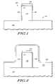
- FIG. 1shows a partial side cross sectional view of one embodiment of a semiconductor wafer during a stage in the manufacture of a transistor with independent gate structures according to the present invention.
- Wafer 101includes a substrate with an insulating layer 103 .
- a structure 104has been formed over insulating layer 103 .
- Structure 104includes a semiconductor structure portion 105 formed over insulating layer 103 , a dielectric portion 111 (e.g. silicon dioxide) formed over semiconductor structure portion 105 and layer 103 , and a nitride portion 109 located over portion 111 and portion 105 .
- structure 104is formed by depositing a layer of semiconductor material over layer 103 , forming a dielectric layer over the semiconductor layer (e.g.
- semiconductor structure portion 105is made of epitaxial silicon bonded on insulating layer 103 .
- portion 105may be made of polysilicon or other semiconductor material.
- structure 104is a fin structure of a FinFET.
- portion 109may be made of other materials (e.g. other dielectrics) that can be utilized as a hard etch mask.
- a conformal polysilicon layer 203is deposited over wafer 101 including over structure 104 .
- polysilicon layer 203is utilized to form independent gate structures of a FinFET transistor.
- layer 203may be made of other gate materials such as e.g. tungsten, titanium, tantalum silicon nitride, silicides such as cobalt or nickel silicides, germanium, silicon germanium, other metals, or combinations thereof.
- a conformal nitride layer 205is then deposited over layer 203 .
- layer 205is used both as an antireflective coating and as a hard mask for etching layer 203 .
- Layer 205may not be included in some embodiments.
- layer 203may be doped prior to the deposition of layer 205 .
- layer 205may be doped with single or multiple implants at various energies, angles, and/or species.
- the left side of layer 203relative to the view shown in FIG. 2 , may doped with a first dopant at a first angle to provide that portion with a first conductivity type
- the right side of the layer 203relative to the view shown in FIG. 2 may be doped at a second angle relative to the view shown in FIG. 2 to provide that portion with a second conductivity type.
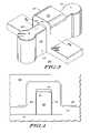
- FIG. 3is a partial isometric view of wafer 101 after layers 205 and 203 have been patterned to form gate structure 301 .
- layers 205 and 203are patterned by the utilization of conventional photolithographic techniques.
- the portion of nitride portion 109 located over structure 104 but not located under gate structure 301is removed. In other embodiments, this portion of nitride portion 109 may be removed at a later stage during manufacture.
- Structure 104includes current terminal regions 303 and 305 located in each end of portion 105 of structure 104 .
- regions 303 and 305serve as the source and drain regions, respectively.
- Regions 303 and 305may be doped at this time by e.g. ion implantation or plasma doping.
- FIG. 4shows a partial cross sectional view of wafer 101 after a deposition of a planar layer 403 over wafer 101 .
- layer 403may be made of e.g., photo resist, spin on glass, or organic antireflective coating material. Layer 403 may be formed by spin on techniques or by chemical vapor deposition techniques followed by chemical mechanical polish or reflow.
- FIG. 5shows wafer 101 after layer 403 has been etched back to a level below the top of portion 505 of nitride layer 203 located over structure 104 to expose portion 505 .
- layer 403may be etched back, e.g., by a conventional dry or wet etch techniques.
- layer 403is at least thick enough to cover portion 503 of layer 205 such that portion 505 of layer 205 may be removed by etching without removing portion 503 .
- the resultant structure of layer 403 as shown in FIG. 5may be formed by the planar deposition of the material of layer 403 to the level shown in FIG. 5 , or other desired level.
- FIG. 6shows the same view as FIG. 5 after portion 505 of nitride layer 205 located over structure 104 has been removed by etching.
- Layer 403protects portion 503 of layer 205 from being removing during the etching of portion 505 .
- the portion of layer 203 previously located under removed portion 505 of layer 205is removed by a non abrasive etching (e.g. wet or dry) to form independent gate structures 701 and 703 .
- Layer 403(along with the remaining portions of layer 205 ) protects portions 707 and 709 of layer 203 from being removed during the etching of layer 203 .
- Gate structures 701 and 703each have a vertical portion located along a sidewall of structure 104 .
- Utilizing a planar layer for the formation of independent gate structuresmay allow a portion of the gate material to be removed to form separate gate structures for a transistor without extra masking steps.
- the planar layerallows for the portion of the gate structure located over structure 104 to be removed without removing the portions of the gate structure used to form the independent gate structures.
- portions of the conformal layers including the gate material located over structure 104are exposed from the planar layer, those portions can be removed e.g. by etching to isolate the gate structures without use of an extra mask step. Accordingly, alignment problems in forming separate gate previously described may be avoided.
- FIG. 8shows the same view as FIG. 7 after the removal of the remaining portions of layers 403 and 205 .
- these layersmay be removed by wet or dry etches. In other embodiments, the remaining portions of layers 403 and 205 are not removed.
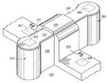
- FIG. 9shows an isometric view of the transistor shown in FIG. 8 .
- spacers and silicide layers of the transistorare formed by conventional semiconductor techniques.
- Regions 903 and 905serve as-current terminal contacts (e.g. as source/drain contacts for FETs).
- regions 907 and 909serve as gate contacts for gate structures 701 and 703 , respectively.
- FIG. 10shows the same view as FIG. 8 after the formation of gate vias 1003 and 1005 over regions 907 and 909 , respectively.
- a low K dielectric material 1009is shown deposited over the resultant transistor structure.
- Other conventional processing stages not shown or described hereinmay be performed on wafer 101 to form other conventional structures (such as e.g. interconnects and passivation layers) of a semiconductor device. Afterwards, the wafer is singulated to separate the integrated circuits of the wafer.
- Transistors with independent gate structuresmay be made by other processes.
- the formation of the planar layer 403 and the removal of the portion of gate material (e.g. in layer 203 ) located over structure 104may be performed after the formation of spacers and/or silicides as described above with respect to FIG. 10 .
- transistors with independent gate structuresmaybe made with out utilizing conformal nitride layer 205 .
- the planar layer 403would be formed such that the top portion of the layer of gate material (e.g. 203 ) located over structure 104 would be exposed for etching.
- independent gate structuresmay be coupled together either by hardwiring (e.g. conductive material extending between the gate structures) or by other transistors which would allow for the gate structures to be selectively coupled together.
- FIGS. 11–17set forth views of a semiconductor wafer during various stages in the manufacture of another embodiment of a transistor with independent gate structures according to the present invention.
- the transistor formedalso includes charge storage locations located between the gates and the channel region of the transistor. As will be describe later, such a transistor may be utilized as a non volatile memory device for storing data in the charge storage locations.
- Wafer 1101includes a substrate having an insulating layer 1103 .
- a structure 1104has been formed over insulating layer 1103 .
- structure 1104is a “fin” structure for a FinFET transistor having charge storage locations.
- Structure 1104includes a semiconductor structure portion 1105 formed over the insulating layer 1103 , a dielectric portion 1111 (e.g. silicon dioxide) formed over semiconductor structure portion 1105 and layer 1103 , and a nitride portion 1109 located over portion 1111 and portion 1105 .
- structure 1104is formed by depositing a layer of semiconductor material over layer 1103 , forming a dielectric layer over the semiconductor material layer (e.g.
- the semiconductor layer, the dielectric layer, and the nitride layerare then patterned to form a structure wherein the sidewalls of the semiconductor layer, the dielectric portion 1111 , and nitride portion 1109 are flush with each other.
- the remaining portion of the semiconductor layeris then trimmed (e.g. with a dry etch having an isotropic component) to recess the sidewalls of remaining semiconductor layer to form portion 1105 as shown in FIG. 11 .
- structure portion 1105is not trimmed.
- structure portion 1105may be doped prior to the patterning of the layer of semiconductor material by conventional semiconductor processing techniques to provide the channel region of portion 105 with a specific conductivity type.
- a dielectric layer 1107is formed on the sidewalls of semiconductor structure portion 1105 .
- the channel region and current terminal regionsare formed in portion 1105 .
- semiconductor structure portion 1105is made of epitaxial silicon bonded on insulating layer 1103 .
- portion 1105may be made of polysilicon or other semiconductor material.
- structure 1104is a fin structure of a FinFET.
- a layer 1203 of charge storage materialis then deposited over wafer 1101 including structure 1104 .
- layer 1203includes a layer of conductive material such as polysilicon (e.g. as with a floating gate transistor).
- layer 1203may include other types of charge storage material including material having a plurality of charge trapping elements (e.g. silicon nitride as with a thin film transistor).
- layer 1203may include discrete charge storage material (e.g. silicon nanocrystals embedded in a layer of dielectric). In some embodiments, the nanocrystals are 2–10 nm in diameter and have a density of 3–10e ⁇ 11/cm ⁇ 2.
- layer 1203may be made of multiple layers such as e.g. a layer of silicon nanocrystals and a layer of silicon nitride deposited over the layer of silicon nanocrystals or a layer of silicon nanocrystals embedded between two layers of dielectric material.
- FIG. 13shows a partial cross sectional view of wafer 1101 after layer 1203 has been etched to remove the portion of layer 1203 located over nitride portion 1109 and located on insulating layer 1103 . Portions of layer 1203 remaining will later be etched to form isolated charge storages structures 1307 and 1305 located on the opposite sidewalls of structure 1104 .
- layer 1203is etched with anisotropic dry etch to form storage structures 1307 and 1305 .
- the charge storage materialis made of a high resistivity material such that there would be little to no leakage current, layer 1203 is not etched. In such embodiments, the charge storage structures having charge storage locations would be part of a contiguous layer 1203 .
- FIG. 14shows a partial cross sectional view of wafer 1101 after a conformal layer 1403 of control dielectric has been deposited over wafer 1101 and after a conformal layer 1407 of gate material has been deposited over layer 1403 .
- gate material layer 1407After the deposition of gate material layer 1407 , the wafer is further processed to form to two gate structures as per a similar process describe above with respect to FIGS. 2–8 .
- a nitride layer(not shown), similar to nitride layer 205 in FIG. 2 , is deposited over layer 1407 .
- the nitride layer and layer 1407is then patterned to form a gate structure similar to gate structure 301 shown in FIG. 3 .
- a portion of charge storage layer 1203 located on the side of dielectric layer 1107 and not underneath the gate structureis etched after the layer 1407 has been etched.
- a planar layer(similar to layer 403 in FIG.
- gate structures 1505 and 1503are formed wherein the portion of the nitride layer located above structure 1104 is exposed (See FIG. 5 and the text discussing thereof).
- the gate material located above structure 1104is then etched to form gate structures 1505 and 1503 (See FIG. 15 ) in a manner similar to that set forth in FIGS. 6–8 and the discussion thereof.
- FIG. 15shows a partial side view of wafer 1101 after the formation of gate structures 1505 and 1503 .
- FIG. 16is a partial isometric view of the transistor structure shown in FIG. 15 .
- Regions 1607 and 1605serve as current terminal regions with 1611 and 1613 serving as current terminal contacts (e.g. as source/drain contacts for FETs) for those regions.
- regions 1620 and 1617serve as gate contacts for gate structures, 1505 and 1503 respectively.
- gate structures 1503 and 1505are doped.
- the material of these gate structuresis doped, in one embodiment, prior to the deposition of the nitride layer (e.g. 205 ) over the layer of gate material.
- the current terminal regions 1607 and 1605are doped after the formation of gate structures 1505 and 1503 to provide a conductivity type that is different from the conductivity type of the channel region of semiconductor structure portion 1105 .
- silicide layers, spacers, gate vias, and current terminal viasare formed over transistor structure 1621 by conventional semiconductor techniques.
- a low K dielectric materiale.g. 1009
- Other conventional processing stages not shown or described hereinmay be performed on wafer 1101 to form other conventional structures (such as e.g. interconnects and passivation layers) of an integrated circuit.
- the resultant transistor structure 1621 shown in FIG. 16can be utilized as a non volatile memory cell having four isolated charge storage locations (two each in charge storage structure 1305 and 1307 , respectively) that can each store one of bit of data.
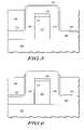
- FIG. 17is a partial cutaway top view of transistor structure 1621 shown in FIG. 16 .
- S Charge storage structure 1305includes two charge storage locations 1709 and 1711
- charge structure 1307includes two charge storage locations 1713 and 1715 . These four charge storage locations may be programmed, read, and or erased by applying voltages to current terminal regions 1605 and 1607 and gate structures 1503 and 1505 .
- the transistor structure 1621functions as two functional MOSFET transistors that share source/drain regions and each have two charge storage-locations.
- Gate structure 1503serves as the gate for one of the functional transistors, and gate structure 1505 serves as the gate of the other functional transistors.
- Charge storage locations 1709 and 1711serve as charge storage locations for the functional transistor having gate structure 1503 as its gate.
- Charge storage locations 1713 and 1715server as charge storage locations for the functional transistor having gate structure 1505 as its gate.
- semiconductor structure portion 1105includes a channel region 1725 (approximately differentiated by the dashed lines) located between current terminal regions 1605 and 1607 .
- Channel region 1725is doped to provide a first conductivity type and current terminal regions 1605 and 1607 are doped to provide a second conductivity type.
- transistor structure 1621when a voltage is applied to gate structure 1503 that exceeds a voltage threshold of the functional transistor associated with gate structure 1503 , an inversion region forms along the sidewall of the channel region 1725 adjacent to gate structure 1503 .
- an inversion layerforms along the sidewall of channel region 1725 adjacent to gate structure 1505 .
- portion 1105is relatively thin between gate structures 1503 and 1505 , the regions where the inversion layers occur may overlap.
- Chargemay be injected into each of the charge storage locations (e.g. by hot carrier injection) to increase the threshold voltage of the functional transistor associated with that charge storage location.
- a positive voltage (Vpp)is applied to gate structure 1503
- 1 ⁇ 2 Vppis applied to current terminal region 1605
- a ground potentialis applied to current terminal region 1607 and gate structure 1505 .
- Each of the charge storage locationsmay be read independently of each other.
- Application of a positive voltage (Vdd) to the gate structure adjacent to a charge storage location and a positive voltage (Vdd) to the current terminal on the opposite side of the charge storage locationwill effectively read the charge stored in the charge storage location without being affected by the charge stored in the other charge storage locations.
- Vddpositive voltage
- Vdddpositive voltage
- a positive chargeis applied to gate structure 1503 and to current terminal region 1607 , with a ground potential (VSS) being applied to gate structure 1505 and current terminal region 1605 .
- the voltage applied to current terminal region 1607is sufficiently positive so that it effectively masks or shadows any charge present in charge storage location 1711 . In this way, the current through the channel region is primarily affected by the charge stored in location 1709 and not by the charge stored in any other charge storage location.
- a hot hole injection techniquemay be utilized. For example, to erase the charge stored in charge storage location 1709 , a negative voltage ( ⁇ Vpp) is applied to gate structure 1503 and a positive voltage (Vpp) is applied to current terminal region 1605 , the current terminal adjacent to charge storage location 1709 . A ground potential (Vss) is applied to current terminal region 1605 and gate structure 1505 .
- ⁇ Vppnegative voltage
- Vpppositive voltage
- Vssground potential
- the charge storage locations of structure 1621may be erased at the same time by applying a negative voltage ( ⁇ Vpp) to gate structures 1503 and 1505 and a positive voltage (Vpp) to current terminal regions 1605 and 1607 .
- ⁇ Vppnegative voltage
- Vpppositive voltage
- program, read, and/or erase techniquesmay be utilized for programming, reading and/or erasing the charge in the charge storage location of transistor structure 1621 .
- other conventional techniques for reading a non volatile memory cells having two storage locationsmay be used.
- transistor structure 1621may be utilized such that it implements only two charge storage locations.
- the first charge storage locationis located in charge storage structure 1305 and the second charge storage location is located in charge storage structure 1307 .
- transistor structure 1621is utilized as two functional transistors with each functional transistor including a charge storage location.
- the charge storage layerwould be made of conducting material (e.g. polysilicon) e.g. as with a floating gate transistor.
- each charge storage structure( 1305 and 1307 ) would independently be able to store a charge, but transistor structure 1621 would be read as a single functional transistor having 4 voltage threshold levels.
- the voltage thresholdwould be a function of the charge stored in both the charge storage structures.
- the charge storage structureswould be programmed with different voltages applied to the gates structures.
- the transistor structurewould be read with a single voltage applied to both gate structures.
- the gate structureswould be preferably of different conductivity types or would have different work functions.
- a transistor structure having gate structures adjacent to the sidewalls of the channel regionmay have other configurations.
- the width, length, and/or height of the channel region 1725may be of other dimensions.
- multiple transistor structuresmay be linked together wherein each transistor structure shares a current terminal region (e.g. 1607 ) with the adjacent transistor structure.
- the channel regions (e.g. 1725 ) and the gate structures (e.g. 1503 and 1505 )would be located between the shared current terminal regions (e.g. 1607 and 1605 ).
- An example of such an implementationmay be represented by the array shown in FIG. 18 wherein the current terminal region of one transistor structure is serves as the current terminal of another transistor structure. For example, referring to FIG.
- a second intermediate structurewould extend from end structure 1630 in the opposite direction (to the left relative to the view shown in FIG. 17 ) as intermediate structure 1631 of structure 1104 extends from end structure 1630 .
- a third intermediate structure(not shown) would extend from end structure 1629 in the opposite direction (to the right relative to the view shown in FIG. 17 ) as intermediate structure 1631 extends from end structure 1629 .
- a pair of gate structures similar to gate structures 1503 and 1505would be adjacent to each sidewall of the second intermediate structure and third intermediate structure, similar to the position of gate structures 1503 and 1505 with respect to intermediate structure 1631 .
- the gate structures 1503 and 1505may have different conductivity types. This may be accomplished in one embodiment by angled implantation of different dopant species. For example gate structure 1505 may be implanted with a P+ dopant and gate structure 1503 may be implanted with an N+ dopant.
- FIG. 18is a circuit diagram of a non volatile memory array implementing the transistor structure 1621 as a memory cell including four storage locations ( 1713 , 1709 , 1715 , and 1711 ).
- array 1801is a non volatile memory array of an integrated circuit device.
- Array 1801includes a number of memory cells with each cell (e.g. 1809 , 1805 , 1807 ) implementing a transistor structure similar to transistor structure 1621 .
- Each cellincludes four storage locations similar to storage locations 1713 , 1709 , 1715 , and 1711 .
- the gate structures (e.g. 1505 and 1503 ) of each cellare coupled to a word line.
- gate structure 1505is couple to word line WL 0 and gate structure 1503 is coupled to word line WL 1 .
- Each current terminal region of a memory cellis coupled to a bitline.
- terminal contact 1611 of terminal regionis coupled to bitline BL 1 and current terminal contact 1613 is coupled to bitline BL 2 .
- the bitlines (BL 0 , BL 1 , BL 2 , and BL 3 ) and the word lines (WL 0 , WL 1 , WL 2 , and WL 3 ) of array 1801are couple to conventional memory array control circuitry (not shown) for controlling the voltages of the lines.
- the memory cellsare arranged in array 1801 in rows and columns. In the embodiment shown, cells 1809 and the cell of transistor structure 1621 are in the same row, and cells, 1809 and 1807 are in the same column.
- FIG. 19sets forth the voltages applied to the bitlines and word lines shown in FIG. 18 for programming, erasing, and reading storage location 1713 .
- Vpp8.0V
- Vss0
- Vdd4.0.
- SAsense amplifier
- BL 1is coupled to a sense amplifier (not shown), as designated by “SA” in the table of FIG. 19 , to determine whether the transistor has been turned on or not. Whether a transistor has been turned on or not is dependent upon whether a charge is stored at the charge storage location (e.g. 1713 ) being read.
- SAsense amplifier
- a voltage of VPP/2is applied to bitline BL 1 and all bitlines located before BL 1 (e.g.
- bitline BL 0locations having a gate coupled to word line WL 0 located before bitline BL 1 (e.g. charge storage location 1821 ) are not programmed.
- a ground voltage VSSis applied to all bitlines located after BL 1 (e.g. BL 2 and BL 3 ) so that no charge storage locations located after bitline BL 2 (e.g. 1823 ) are inadvertently programmed.
- the charge storage locations of array 1801may be erased in a block erase function. In these embodiments, a positive voltage is applied to all bitlines and a negative voltage is applied to all word lines.
- FIG. 20sets forth voltages applied to the bitlines and word lines shown in FIG. 18 for programming, erasing, and reading storage location 1711 .
- the gate of a cell opposite of the charge storage location being programmed, erased, or readis biased at ground (VSS) during these operations.
- gate structure 1503which is opposite of charge storage location 1713 , is biased at VSS during program, erase, and read operations of location 1713 .
- FIGS. 21 and 22set forth voltages that are applied to the bitlines and word lines of array 1801 in another embodiment for programming, erasing, and reading the charge storage locations of 1801 .
- the opposing gate to the charge storage location of a cell being programmedis biased at the opposite voltage of the gate of the cell associated with that location.
- a positive voltage VPPis applied to the word line (WL 0 ), which is coupled to gate structure 1505 and is associated with charge storage location 1713
- ⁇ VPPis applied to word line WL 1 , which is coupled gate structure 1503 and is opposite to charge storage location 1713 .
- the width and conductivity of the channel regions of the transistor structuresare such that the potential of the channel region adjacent to a gate structure is influenced by the opposing gate structure.
- VPPmay be 6.0 volts. Accordingly, because this embodiment allows for a reduction in the program voltage, lower programming voltages may be utilized. In some embodiments, reducing the programming voltage may allow for a reduction in the area required for circuitry to provide the program voltage.
- the opposite gate of a charge storage locationcan provide a transistor such as e.g. a FinFET with a voltage control circuit that effectively acts like as a well voltage control circuit for a planar CMOS transistor.
- a transistorsuch as e.g. a FinFET
- the voltage of the opposing gatecan be controlled independently of gates in other rows of the array. This may allow for the use of more advanced program and erase techniques for an array than would be possible with other types of charge storage transistors.
- One advantage that may occur with the array shown in FIG. 18is that more charge storage locations may be implemented in a given area than with planar CMOS NVM cells. Furthermore, with the array of FIG. 18 , because 4 independent storage locations are programmable utilizing just two current terminal contacts, the transistors may be more closely placed in an array. In some embodiments, a transistor structure similar to transistor structure 1621 may be easily implemented in an integrated circuit having devices implementing FinFET technology or other types of silicon on insulator technology.
- transistor structure 1261may be modified to have only one charge storage structure between a gate and the sidewall of the channel region.
- the opposing sidewallwould not have a charge storage structure between it and the opposing gate.
- the opposing gatewould serve as an effective well bias voltage control circuit.
- transistor structuressuch as those describe above may be implemented in memory arrays having other configurations.
- a memory cell having two independent gate structures adjacent to opposing sidewalls of a semiconductor structure and having charge storage locations located between the gate structures and the sidewallsmaybe made by other semiconductor processes other than that set forth in this specification, including other conventional processes for forming independent gate structures.
- a method of making a semiconductor deviceincludes providing a substrate and a semiconductor structure over the substrate.
- the semiconductor structurehas a first sidewall, a second sidewall, and a top surface.
- the methodalso includes depositing at least one substantially conformal layer over the substrate.
- the at least one substantially conformal layerincludes at least a layer of gate material.
- the at least one substantially conformal layerhas a top surface at a height over the semiconductor structure.
- the methodfurther includes forming a substantially planar layer over the substrate below the height of the top surface of the at least one substantially conformal layer over the semiconductor structure and non-abrasive etching through the layer of gate material over the top surface of the semiconductor structure.
- a method of making a semiconductor deviceincludes providing a substrate and a semiconductor structure over the substrate.
- the semiconductor structurehas a first sidewall, a second sidewall, and a top surface.
- the methodalso includes depositing a first substantially conformal layer of gate material over the substrate and over the semiconductor structure, depositing a second substantially conformal layer of a material over the first substantially conformal layer, and forming a substantially planar layer over the substrate after depositing the second substantially conformal layer.
- the methodstill further includes etching through the first substantially conformal layer over the top surface of the semiconductor structure, etching through the second substantially conformal layer over the top surface of the semiconductor structure, and forming a contact to a portion of the first substantially conformal layer.
- a method of forming a semiconductor structureincludes providing a substrate and forming a semiconductor fin on the substrate.
- the finhas a first and second sidewalls.
- the methodalso includes forming a layer of charge storage material over the substrate.
- the layer of charge storage materialincludes a first portion adjacent to the first sidewall of the fin and a second portion adjacent to the second sidewall of the fin.
- the methodstill further includes forming a layer of gate material over the substrate after the forming the layer of charge storage material.
- the layer of gate materialincludes a first portion adjacent to the first sidewall of the fin and a second portion adjacent the second sidewall of the fin.
- the methodstill further includes removing the layer of gate material over the semiconductor fin.
Landscapes
- Engineering & Computer Science (AREA)
- Physics & Mathematics (AREA)
- Condensed Matter Physics & Semiconductors (AREA)
- General Physics & Mathematics (AREA)
- Manufacturing & Machinery (AREA)
- Computer Hardware Design (AREA)
- Microelectronics & Electronic Packaging (AREA)
- Power Engineering (AREA)
- Non-Volatile Memory (AREA)
- Semiconductor Memories (AREA)
- Thin Film Transistor (AREA)
- Electrodes Of Semiconductors (AREA)
Abstract
Description
Claims (39)
Priority Applications (6)
| Application Number | Priority Date | Filing Date | Title |
|---|---|---|---|
| US10/443,375US7192876B2 (en) | 2003-05-22 | 2003-05-22 | Transistor with independent gate structures |
| CNB2004800141381ACN100466186C (en) | 2003-05-22 | 2004-04-16 | Method for fabricating transistor with independent gate structure |
| JP2006532424AJP5350589B2 (en) | 2003-05-22 | 2004-04-16 | Transistor with individual gate structure |
| KR1020057022325AKR101079562B1 (en) | 2003-05-22 | 2004-04-16 | Transistor with independent gate structures |
| PCT/US2004/011869WO2004107399A2 (en) | 2003-05-22 | 2004-04-16 | Transistor with independant gate structures |
| TW093111745ATWI361489B (en) | 2003-05-22 | 2004-04-27 | Transistor with independent gate structures |
Applications Claiming Priority (1)
| Application Number | Priority Date | Filing Date | Title |
|---|---|---|---|
| US10/443,375US7192876B2 (en) | 2003-05-22 | 2003-05-22 | Transistor with independent gate structures |
Publications (2)
| Publication Number | Publication Date |
|---|---|
| US20040235300A1 US20040235300A1 (en) | 2004-11-25 |
| US7192876B2true US7192876B2 (en) | 2007-03-20 |
Family
ID=33450398
Family Applications (1)
| Application Number | Title | Priority Date | Filing Date |
|---|---|---|---|
| US10/443,375Expired - Fee RelatedUS7192876B2 (en) | 2003-05-22 | 2003-05-22 | Transistor with independent gate structures |
Country Status (6)
| Country | Link |
|---|---|
| US (1) | US7192876B2 (en) |
| JP (1) | JP5350589B2 (en) |
| KR (1) | KR101079562B1 (en) |
| CN (1) | CN100466186C (en) |
| TW (1) | TWI361489B (en) |
| WO (1) | WO2004107399A2 (en) |
Cited By (11)
| Publication number | Priority date | Publication date | Assignee | Title |
|---|---|---|---|---|
| US20050001216A1 (en)* | 2000-10-18 | 2005-01-06 | Adkisson James W. | Method of fabricating semiconductor side wall fin |
| US20070161170A1 (en)* | 2005-12-16 | 2007-07-12 | Orlowski Marius K | Transistor with immersed contacts and methods of forming thereof |
| US20080206934A1 (en)* | 2007-02-23 | 2008-08-28 | Jones Robert E | Forming semiconductor fins using a sacrificial fin |
| US20080315315A1 (en)* | 2006-01-06 | 2008-12-25 | Freescale Semiconductor, Inc. | Electronic device including a gated diode |
| US20090041406A1 (en)* | 2007-08-08 | 2009-02-12 | Thomas Schulz | Integrated circuit including non-planar structure and waveguide |
| US20090309139A1 (en)* | 2008-06-13 | 2009-12-17 | International Business Machines Corporation | Asymmetric gate electrode and method of manufacture |
| US20100289085A1 (en)* | 2009-05-14 | 2010-11-18 | International Business Machines Corporation | Asymmetric Semiconductor Devices and Method of Fabricating |
| US8866214B2 (en) | 2011-10-12 | 2014-10-21 | International Business Machines Corporation | Vertical transistor having an asymmetric gate |
| US9214529B2 (en) | 2011-03-14 | 2015-12-15 | Globalfoundries Inc. | Fin Fet device with independent control gate |
| US10128377B2 (en) | 2017-02-24 | 2018-11-13 | International Business Machines Corporation | Independent gate FinFET with backside gate contact |
| US11239374B2 (en)* | 2018-11-29 | 2022-02-01 | Commissariat A L'energie Atomique Et Aux Energies Alternatives | Method of fabricating a field effect transistor |
Families Citing this family (44)
| Publication number | Priority date | Publication date | Assignee | Title |
|---|---|---|---|---|
| DE10220923B4 (en)* | 2002-05-10 | 2006-10-26 | Infineon Technologies Ag | Method for producing a non-volatile flash semiconductor memory |
| US6963104B2 (en)* | 2003-06-12 | 2005-11-08 | Advanced Micro Devices, Inc. | Non-volatile memory device |
| JP2005086024A (en)* | 2003-09-09 | 2005-03-31 | Toshiba Corp | Semiconductor device and method for manufacturing same |
| KR100515061B1 (en)* | 2003-10-31 | 2005-09-14 | 삼성전자주식회사 | Semiconductor devices having a fin field effect transistor and methods for forming the same |
| US7098502B2 (en)* | 2003-11-10 | 2006-08-29 | Freescale Semiconductor, Inc. | Transistor having three electrically isolated electrodes and method of formation |
| US6933558B2 (en)* | 2003-12-04 | 2005-08-23 | Advanced Micro Devices, Inc. | Flash memory device |
| US7629640B2 (en)* | 2004-05-03 | 2009-12-08 | The Regents Of The University Of California | Two bit/four bit SONOS flash memory cell |
| KR100541657B1 (en)* | 2004-06-29 | 2006-01-11 | 삼성전자주식회사 | Multi-gate transistor fabrication method and multi-gate transistor fabricated thereby |
| US7259420B2 (en)* | 2004-07-28 | 2007-08-21 | International Business Machines Corporation | Multiple-gate device with floating back gate |
| US7388257B2 (en)* | 2004-09-01 | 2008-06-17 | International Business Machines Corporation | Multi-gate device with high k dielectric for channel top surface |
| KR100598049B1 (en)* | 2004-10-28 | 2006-07-07 | 삼성전자주식회사 | Semiconductor device including multi-bit nonvolatile memory cell and manufacturing method thereof |
| DE102004061518A1 (en)* | 2004-12-21 | 2006-06-29 | Infineon Technologies Ag | Fin field effect transistor manufacturing method, involves producing auxiliary layer, where auxiliary layer covers part of electrically conductive layer and does not cover part of conductive layer that is arranged over top surface |
| US7470951B2 (en)* | 2005-01-31 | 2008-12-30 | Freescale Semiconductor, Inc. | Hybrid-FET and its application as SRAM |
| US20060197140A1 (en)* | 2005-03-04 | 2006-09-07 | Freescale Semiconductor, Inc. | Vertical transistor NVM with body contact structure and method |
| US7301741B2 (en)* | 2005-05-17 | 2007-11-27 | Freescale Semiconductor, Inc. | Integrated circuit with multiple independent gate field effect transistor (MIGFET) rail clamp circuit |
| US7101763B1 (en) | 2005-05-17 | 2006-09-05 | International Business Machines Corporation | Low capacitance junction-isolation for bulk FinFET technology |
| KR100645065B1 (en)* | 2005-06-23 | 2006-11-10 | 삼성전자주식회사 | Fin Field Effect Transistor, Nonvolatile Memory Device Having Same and Forming Method Thereof |
| JP2009510721A (en)* | 2005-09-28 | 2009-03-12 | エヌエックスピー ビー ヴィ | Double-gate nonvolatile memory device and manufacturing method thereof |
| US7452768B2 (en) | 2005-10-25 | 2008-11-18 | Freescale Semiconductor, Inc. | Multiple device types including an inverted-T channel transistor and method therefor |
| US8513066B2 (en)* | 2005-10-25 | 2013-08-20 | Freescale Semiconductor, Inc. | Method of making an inverted-T channel transistor |
| JP4761946B2 (en)* | 2005-11-22 | 2011-08-31 | 株式会社東芝 | NONVOLATILE SEMICONDUCTOR MEMORY ELEMENT, ITS MANUFACTURING METHOD, AND SEMICONDUCTOR INTEGRATED CIRCUIT DEVICE INCLUDING NONVOLATILE SEMICONDUCTOR MEMORY ELEMENT |
| WO2007070808A2 (en)* | 2005-12-12 | 2007-06-21 | The Regents Of The University Of California | Multi-bit-per-cell nvm structures and architecture |
| EP2165356A1 (en)* | 2005-12-15 | 2010-03-24 | Nxp B.V. | Non-volatile memory device having a gap in the tunnel insulating layer and method of manufacturing the same |
| FR2895835B1 (en) | 2005-12-30 | 2008-05-09 | Commissariat Energie Atomique | ACHIEVING A MULTI-BRANCH CHANNEL STRUCTURE OF A TRANSISTOR GRID AND MEANS FOR ISOLATING THIS GRID FROM THE SOURCE AND DRAIN REGIONS |
| US7323373B2 (en)* | 2006-01-25 | 2008-01-29 | Freescale Semiconductor, Inc. | Method of forming a semiconductor device with decreased undercutting of semiconductor material |
| US7544980B2 (en)* | 2006-01-27 | 2009-06-09 | Freescale Semiconductor, Inc. | Split gate memory cell in a FinFET |
| US7535060B2 (en)* | 2006-03-08 | 2009-05-19 | Freescale Semiconductor, Inc. | Charge storage structure formation in transistor with vertical channel region |
| US20070212832A1 (en)* | 2006-03-08 | 2007-09-13 | Freescale Semiconductor Inc. | Method for making a multibit transistor |
| US7566623B2 (en)* | 2007-02-02 | 2009-07-28 | Freescale Semiconductor, Inc. | Electronic device including a semiconductor fin having a plurality of gate electrodes and a process for forming the electronic device |
| WO2008110497A1 (en) | 2007-03-14 | 2008-09-18 | Nxp B.V. | Finfet with two independent gates and method for fabricating the same |
| US7859044B2 (en)* | 2007-07-24 | 2010-12-28 | International Business Machines Corporation | Partially gated FINFET with gate dielectric on only one sidewall |
| TW200913162A (en)* | 2007-09-11 | 2009-03-16 | Univ Nat Chiao Tung | Nonvolatile memory device with nanowire channel and a method for fabricating the same |
| FR2921757B1 (en) | 2007-09-28 | 2009-12-18 | Commissariat Energie Atomique | DOUBLE-GRID TRANSISTOR STRUCTURE WITH MULTI-BRANCH CHANNEL |
| WO2009072983A1 (en)* | 2007-12-07 | 2009-06-11 | Agency For Science, Technology And Research | Memory cell and methods of manufacturing thereof |
| US20110079840A1 (en)* | 2009-10-01 | 2011-04-07 | Macronix International Co., Ltd. | Memory cell and manufacturing method thereof and memory structure |
| JP5228021B2 (en)* | 2010-09-29 | 2013-07-03 | 株式会社東芝 | Semiconductor memory device |
| JP5624567B2 (en)* | 2012-02-03 | 2014-11-12 | 株式会社東芝 | Nonvolatile semiconductor memory device and manufacturing method thereof |
| JP6220641B2 (en)* | 2012-11-15 | 2017-10-25 | 株式会社半導体エネルギー研究所 | Semiconductor device |
| US9276114B2 (en) | 2013-02-01 | 2016-03-01 | Taiwan Semiconductor Manufacturing Company, Ltd. | FinFET with dual workfunction gate structure |
| US9373620B2 (en)* | 2014-09-12 | 2016-06-21 | Taiwan Semiconductor Manufacturing Co., Ltd. | Series connected transistor structure and method of manufacturing the same |
| US9305974B1 (en)* | 2015-04-16 | 2016-04-05 | Stmicroelectronics, Inc. | High density resistive random access memory (RRAM) |
| US9779959B2 (en) | 2015-09-17 | 2017-10-03 | Taiwan Semiconductor Manufacturing Co., Ltd. | Structure and formation method of semiconductor device structure |
| CN105632936B (en)* | 2016-03-22 | 2018-10-16 | 上海华力微电子有限公司 | A kind of preparation method of bigrid fin formula field effect transistor |
| KR102668105B1 (en)* | 2018-11-05 | 2024-05-23 | 한국전자통신연구원 | Thin film trasistor and a method for manufacturing the same |
Citations (58)
| Publication number | Priority date | Publication date | Assignee | Title |
|---|---|---|---|---|
| US4714519A (en) | 1987-03-30 | 1987-12-22 | Motorola, Inc. | Method for fabricating MOS transistors having gates with different work functions |
| US4859623A (en) | 1988-02-04 | 1989-08-22 | Amoco Corporation | Method of forming vertical gate thin film transistors in liquid crystal array |
| US4868617A (en) | 1988-04-25 | 1989-09-19 | Elite Semiconductor & Sytems International, Inc. | Gate controllable lightly doped drain mosfet devices |
| US5063172A (en) | 1990-06-28 | 1991-11-05 | National Semiconductor Corporation | Manufacture of a split-gate EPROM cell using polysilicon spacers |
| US5089870A (en) | 1989-06-19 | 1992-02-18 | L'etat Francais Represente Par Le Ministre Des Postes, Des Telecommunications Et De L'espace (Centre National D'etudes Des Telecommunications) | Soi mos transistor with a substrate-source connection |
| US5212105A (en) | 1989-05-24 | 1993-05-18 | Kabushiki Kaisha Toshiba | Semiconductor device manufacturing method and semiconductor device manufactured thereby |
| US5284784A (en) | 1991-10-02 | 1994-02-08 | National Semiconductor Corporation | Buried bit-line source-side injection flash memory cell |
| US5324960A (en) | 1993-01-19 | 1994-06-28 | Motorola, Inc. | Dual-transistor structure and method of formation |
| US5631482A (en) | 1994-09-30 | 1997-05-20 | United Microelectronics Corporation | Flash EEPROM memory cell with polysilicon source/drain |
| US5631176A (en) | 1995-07-13 | 1997-05-20 | Lsi Logic Corporation | Method of making combined JFET & MOS transistor device |
| US5641698A (en) | 1994-11-07 | 1997-06-24 | United Microelectronics Corporation | Method of fabricating FET device with double spacer |
| US5689127A (en) | 1996-03-05 | 1997-11-18 | International Business Machines Corporation | Vertical double-gate field effect transistor |
| US5804848A (en) | 1995-01-20 | 1998-09-08 | Sony Corporation | Field effect transistor having multiple gate electrodes surrounding the channel region |
| US5831319A (en) | 1995-12-04 | 1998-11-03 | Chartered Semiconductor | Conductive spacer lightly doped drain (LDD) for hot carrier effect (HCE) control |
| US5912492A (en) | 1995-12-29 | 1999-06-15 | Taiwan Semiconductor Manufacturing Company, Ltd. | Integrated circuit structure incorporating a metal oxide semiconductor field effect transistor (MOSFET) having improved hot carrier immunity |
| US5915176A (en) | 1996-12-26 | 1999-06-22 | Lg Semicon Co., Ltd. | Method of making floating gate based memory device |
| US6011725A (en) | 1997-08-01 | 2000-01-04 | Saifun Semiconductors, Ltd. | Two bit non-volatile electrically erasable and programmable semiconductor memory cell utilizing asymmetrical charge trapping |
| US6031266A (en) | 1996-11-11 | 2000-02-29 | Kabushiki Kaisha Toshiba | Semiconductor device with conductive sidewall film |
| US6043545A (en) | 1998-02-07 | 2000-03-28 | United Microelectronics Corp. | MOSFET device with two spacers |
| WO2000021118A2 (en) | 1998-10-07 | 2000-04-13 | Forschungszentrum Jülich GmbH | Method for producing a double gate of a vertical mosfet |
| US6093612A (en) | 1997-05-24 | 2000-07-25 | Lg Semicon Co., Ltd. | Metal oxide silicon field effect transistor (MOSFET) and fabrication method of same |
| US6097065A (en) | 1998-03-30 | 2000-08-01 | Micron Technology, Inc. | Circuits and methods for dual-gated transistors |
| US6150687A (en) | 1997-07-08 | 2000-11-21 | Micron Technology, Inc. | Memory cell having a vertical transistor with buried source/drain and dual gates |
| US6207519B1 (en) | 1997-10-08 | 2001-03-27 | Samsung Electronics Co., Ltd | Method of making semiconductor device having double spacer |
| US6300182B1 (en) | 2000-12-11 | 2001-10-09 | Advanced Micro Devices, Inc. | Field effect transistor having dual gates with asymmetrical doping for reduced threshold voltage |
| US6312995B1 (en) | 1999-03-08 | 2001-11-06 | Advanced Micro Devices, Inc. | MOS transistor with assisted-gates and ultra-shallow “Psuedo” source and drain extensions for ultra-large-scale integration |
| US6330184B1 (en) | 2000-02-01 | 2001-12-11 | Motorola, Inc. | Method of operating a semiconductor device |
| US6355961B1 (en) | 1998-09-01 | 2002-03-12 | Micron Technology, Inc. | Structure and method for improved signal processing |
| US6372559B1 (en) | 2000-11-09 | 2002-04-16 | International Business Machines Corporation | Method for self-aligned vertical double-gate MOSFET |
| US6396108B1 (en) | 2000-11-13 | 2002-05-28 | Advanced Micro Devices, Inc. | Self-aligned double gate silicon-on-insulator (SOI) device |
| US6399451B1 (en) | 1998-09-16 | 2002-06-04 | Samsung Electronics Co., Ltd. | Semiconductor device having gate spacer containing conductive layer and manufacturing method therefor |
| US6413802B1 (en) | 2000-10-23 | 2002-07-02 | The Regents Of The University Of California | Finfet transistor structures having a double gate channel extending vertically from a substrate and methods of manufacture |
| DE10125967C1 (en) | 2001-05-29 | 2002-07-11 | Infineon Technologies Ag | DRAM cell arrangement used for a semiconductor storage device comprises a matrix arrangement of storage cells stacked over each other as layers, and a capacitor connected to the MOS transistor |
| US6424001B1 (en) | 2001-02-09 | 2002-07-23 | Micron Technology, Inc. | Flash memory with ultra thin vertical body transistors |
| US6433609B1 (en) | 2001-11-19 | 2002-08-13 | International Business Machines Corporation | Double-gate low power SOI active clamp network for single power supply and multiple power supply applications |
| US6458662B1 (en) | 2001-04-04 | 2002-10-01 | Advanced Micro Devices, Inc. | Method of fabricating a semiconductor device having an asymmetrical dual-gate silicon-germanium (SiGe) channel MOSFET and a device thereby formed |
| US6472258B1 (en) | 2000-11-13 | 2002-10-29 | International Business Machines Corporation | Double gate trench transistor |
| US20030034518A1 (en) | 1999-03-08 | 2003-02-20 | Kabushiki Kaisha Toshiba | Method for manufacturing semiconductor memory |
| US20030038308A1 (en) | 2000-04-03 | 2003-02-27 | Hynix Semiconductor, Inc. | Low-resistance gate transistor and method for fabricating the same |
| US6531350B2 (en)* | 2001-02-22 | 2003-03-11 | Halo, Inc. | Twin MONOS cell fabrication method and array organization |
| US6562676B1 (en) | 2001-12-14 | 2003-05-13 | Advanced Micro Devices, Inc. | Method of forming differential spacers for individual optimization of n-channel and p-channel transistors |
| US6563151B1 (en) | 2000-09-05 | 2003-05-13 | Samsung Electronics Co., Ltd. | Field effect transistors having gate and sub-gate electrodes that utilize different work function materials and methods of forming same |
| US6566208B2 (en) | 2001-07-25 | 2003-05-20 | Chartered Semiconductor Manufacturing Ltd. | Method to form elevated source/drain using poly spacer |
| US6566682B2 (en) | 2001-02-09 | 2003-05-20 | Micron Technology, Inc. | Programmable memory address and decode circuits with ultra thin vertical body transistors |
| US20030113970A1 (en) | 2001-12-14 | 2003-06-19 | Fried David M. | Implanted asymmetric doped polysilicon gate FinFET |
| US6583469B1 (en) | 2002-01-28 | 2003-06-24 | International Business Machines Corporation | Self-aligned dog-bone structure for FinFET applications and methods to fabricate the same |
| US20030170969A1 (en) | 1999-09-22 | 2003-09-11 | Emi Ishida | Semiconductor processing employing a semiconducting spacer |
| US20030178670A1 (en) | 2002-03-19 | 2003-09-25 | International Business Machines Corporation | Finfet CMOS with NVRAM capability |
| US20030183872A1 (en) | 2002-03-27 | 2003-10-02 | Takashi Miida | Semiconductor device and semiconductor memory using the same |
| US6656825B2 (en) | 2002-04-30 | 2003-12-02 | Advanced Micro Devices, Inc. | Semiconductor device having an improved local interconnect structure and a method for forming such a device |
| US6661057B1 (en) | 1998-04-07 | 2003-12-09 | Advanced Micro Devices Inc | Tri-level segmented control transistor and fabrication method |
| US6689650B2 (en)* | 2001-09-27 | 2004-02-10 | International Business Machines Corporation | Fin field effect transistor with self-aligned gate |
| US6768158B2 (en)* | 2001-09-04 | 2004-07-27 | Korea Advanced Institute Of Science And Technology | Flash memory element and manufacturing method thereof |
| US6787864B2 (en)* | 2002-09-30 | 2004-09-07 | Advanced Micro Devices, Inc. | Mosfets incorporating nickel germanosilicided gate and methods for their formation |
| US6816414B1 (en) | 2003-07-31 | 2004-11-09 | Freescale Semiconductor, Inc. | Nonvolatile memory and method of making same |
| US6846734B2 (en)* | 2002-11-20 | 2005-01-25 | International Business Machines Corporation | Method and process to make multiple-threshold metal gates CMOS technology |
| US20050280103A1 (en) | 2002-06-07 | 2005-12-22 | Amberwave Systems Corporation | Strained-semiconductor-on-insulator finFET device structures |
| US7005710B1 (en) | 1996-10-31 | 2006-02-28 | Micron Technology, Inc. | Transistors having controlled conductive spacers, uses of such transistors and methods of making such transistors |
Family Cites Families (6)
| Publication number | Priority date | Publication date | Assignee | Title |
|---|---|---|---|---|
| US3720216A (en)* | 1971-09-27 | 1973-03-13 | Union Carbide Corp | Method for reducing the dynamic drag of a turbulent aqueous stream |
| JP3046376B2 (en)* | 1991-03-29 | 2000-05-29 | 株式会社東芝 | Nonvolatile semiconductor memory device |
| JP3270875B2 (en)* | 1993-11-30 | 2002-04-02 | ソニー株式会社 | Method for manufacturing MOS transistor |
| CN1228817C (en)* | 2001-04-02 | 2005-11-23 | 华邦电子股份有限公司 | Method for manufacturing semiconductor component with double gate oxide layer |
| US20060157709A1 (en)* | 2002-08-20 | 2006-07-20 | Koninklijke Philips Electronics N.V. | Thin film transistor |
| US6756643B1 (en)* | 2003-06-12 | 2004-06-29 | Advanced Micro Devices, Inc. | Dual silicon layer for chemical mechanical polishing planarization |
- 2003
- 2003-05-22USUS10/443,375patent/US7192876B2/ennot_activeExpired - Fee Related
- 2004
- 2004-04-16KRKR1020057022325Apatent/KR101079562B1/ennot_activeExpired - Fee Related
- 2004-04-16JPJP2006532424Apatent/JP5350589B2/ennot_activeExpired - Fee Related
- 2004-04-16CNCNB2004800141381Apatent/CN100466186C/ennot_activeExpired - Fee Related
- 2004-04-16WOPCT/US2004/011869patent/WO2004107399A2/enactiveApplication Filing
- 2004-04-27TWTW093111745Apatent/TWI361489B/ennot_activeIP Right Cessation
Patent Citations (60)
| Publication number | Priority date | Publication date | Assignee | Title |
|---|---|---|---|---|
| US4714519A (en) | 1987-03-30 | 1987-12-22 | Motorola, Inc. | Method for fabricating MOS transistors having gates with different work functions |
| US4859623A (en) | 1988-02-04 | 1989-08-22 | Amoco Corporation | Method of forming vertical gate thin film transistors in liquid crystal array |
| US4868617A (en) | 1988-04-25 | 1989-09-19 | Elite Semiconductor & Sytems International, Inc. | Gate controllable lightly doped drain mosfet devices |
| US5212105A (en) | 1989-05-24 | 1993-05-18 | Kabushiki Kaisha Toshiba | Semiconductor device manufacturing method and semiconductor device manufactured thereby |
| US5089870A (en) | 1989-06-19 | 1992-02-18 | L'etat Francais Represente Par Le Ministre Des Postes, Des Telecommunications Et De L'espace (Centre National D'etudes Des Telecommunications) | Soi mos transistor with a substrate-source connection |
| US5063172A (en) | 1990-06-28 | 1991-11-05 | National Semiconductor Corporation | Manufacture of a split-gate EPROM cell using polysilicon spacers |
| US5284784A (en) | 1991-10-02 | 1994-02-08 | National Semiconductor Corporation | Buried bit-line source-side injection flash memory cell |
| US5324960A (en) | 1993-01-19 | 1994-06-28 | Motorola, Inc. | Dual-transistor structure and method of formation |
| US5631482A (en) | 1994-09-30 | 1997-05-20 | United Microelectronics Corporation | Flash EEPROM memory cell with polysilicon source/drain |
| US5641698A (en) | 1994-11-07 | 1997-06-24 | United Microelectronics Corporation | Method of fabricating FET device with double spacer |
| US5804848A (en) | 1995-01-20 | 1998-09-08 | Sony Corporation | Field effect transistor having multiple gate electrodes surrounding the channel region |
| US5631176A (en) | 1995-07-13 | 1997-05-20 | Lsi Logic Corporation | Method of making combined JFET & MOS transistor device |
| US5831319A (en) | 1995-12-04 | 1998-11-03 | Chartered Semiconductor | Conductive spacer lightly doped drain (LDD) for hot carrier effect (HCE) control |
| US5912492A (en) | 1995-12-29 | 1999-06-15 | Taiwan Semiconductor Manufacturing Company, Ltd. | Integrated circuit structure incorporating a metal oxide semiconductor field effect transistor (MOSFET) having improved hot carrier immunity |
| US5689127A (en) | 1996-03-05 | 1997-11-18 | International Business Machines Corporation | Vertical double-gate field effect transistor |
| US7005710B1 (en) | 1996-10-31 | 2006-02-28 | Micron Technology, Inc. | Transistors having controlled conductive spacers, uses of such transistors and methods of making such transistors |
| US6031266A (en) | 1996-11-11 | 2000-02-29 | Kabushiki Kaisha Toshiba | Semiconductor device with conductive sidewall film |
| US5915176A (en) | 1996-12-26 | 1999-06-22 | Lg Semicon Co., Ltd. | Method of making floating gate based memory device |
| US6093612A (en) | 1997-05-24 | 2000-07-25 | Lg Semicon Co., Ltd. | Metal oxide silicon field effect transistor (MOSFET) and fabrication method of same |
| US6150687A (en) | 1997-07-08 | 2000-11-21 | Micron Technology, Inc. | Memory cell having a vertical transistor with buried source/drain and dual gates |
| US6011725A (en) | 1997-08-01 | 2000-01-04 | Saifun Semiconductors, Ltd. | Two bit non-volatile electrically erasable and programmable semiconductor memory cell utilizing asymmetrical charge trapping |
| US6207519B1 (en) | 1997-10-08 | 2001-03-27 | Samsung Electronics Co., Ltd | Method of making semiconductor device having double spacer |
| US6043545A (en) | 1998-02-07 | 2000-03-28 | United Microelectronics Corp. | MOSFET device with two spacers |
| US6097065A (en) | 1998-03-30 | 2000-08-01 | Micron Technology, Inc. | Circuits and methods for dual-gated transistors |
| US6414356B1 (en) | 1998-03-30 | 2002-07-02 | Micron Technology, Inc. | Circuits and methods for dual-gated transistors |
| US6661057B1 (en) | 1998-04-07 | 2003-12-09 | Advanced Micro Devices Inc | Tri-level segmented control transistor and fabrication method |
| US6355961B1 (en) | 1998-09-01 | 2002-03-12 | Micron Technology, Inc. | Structure and method for improved signal processing |
| US6399451B1 (en) | 1998-09-16 | 2002-06-04 | Samsung Electronics Co., Ltd. | Semiconductor device having gate spacer containing conductive layer and manufacturing method therefor |
| WO2000021118A2 (en) | 1998-10-07 | 2000-04-13 | Forschungszentrum Jülich GmbH | Method for producing a double gate of a vertical mosfet |
| US20030034518A1 (en) | 1999-03-08 | 2003-02-20 | Kabushiki Kaisha Toshiba | Method for manufacturing semiconductor memory |
| US6312995B1 (en) | 1999-03-08 | 2001-11-06 | Advanced Micro Devices, Inc. | MOS transistor with assisted-gates and ultra-shallow “Psuedo” source and drain extensions for ultra-large-scale integration |
| US20030170969A1 (en) | 1999-09-22 | 2003-09-11 | Emi Ishida | Semiconductor processing employing a semiconducting spacer |
| US6330184B1 (en) | 2000-02-01 | 2001-12-11 | Motorola, Inc. | Method of operating a semiconductor device |
| US20030038308A1 (en) | 2000-04-03 | 2003-02-27 | Hynix Semiconductor, Inc. | Low-resistance gate transistor and method for fabricating the same |
| US6563151B1 (en) | 2000-09-05 | 2003-05-13 | Samsung Electronics Co., Ltd. | Field effect transistors having gate and sub-gate electrodes that utilize different work function materials and methods of forming same |
| US6413802B1 (en) | 2000-10-23 | 2002-07-02 | The Regents Of The University Of California | Finfet transistor structures having a double gate channel extending vertically from a substrate and methods of manufacture |
| US6372559B1 (en) | 2000-11-09 | 2002-04-16 | International Business Machines Corporation | Method for self-aligned vertical double-gate MOSFET |
| US6472258B1 (en) | 2000-11-13 | 2002-10-29 | International Business Machines Corporation | Double gate trench transistor |
| US6396108B1 (en) | 2000-11-13 | 2002-05-28 | Advanced Micro Devices, Inc. | Self-aligned double gate silicon-on-insulator (SOI) device |
| US6300182B1 (en) | 2000-12-11 | 2001-10-09 | Advanced Micro Devices, Inc. | Field effect transistor having dual gates with asymmetrical doping for reduced threshold voltage |
| US6566682B2 (en) | 2001-02-09 | 2003-05-20 | Micron Technology, Inc. | Programmable memory address and decode circuits with ultra thin vertical body transistors |
| US6720216B2 (en) | 2001-02-09 | 2004-04-13 | Micron Technology, Inc. | Programmable memory address and decode circuits with vertical body transistors |
| US6424001B1 (en) | 2001-02-09 | 2002-07-23 | Micron Technology, Inc. | Flash memory with ultra thin vertical body transistors |
| US6531350B2 (en)* | 2001-02-22 | 2003-03-11 | Halo, Inc. | Twin MONOS cell fabrication method and array organization |
| US6458662B1 (en) | 2001-04-04 | 2002-10-01 | Advanced Micro Devices, Inc. | Method of fabricating a semiconductor device having an asymmetrical dual-gate silicon-germanium (SiGe) channel MOSFET and a device thereby formed |
| DE10125967C1 (en) | 2001-05-29 | 2002-07-11 | Infineon Technologies Ag | DRAM cell arrangement used for a semiconductor storage device comprises a matrix arrangement of storage cells stacked over each other as layers, and a capacitor connected to the MOS transistor |
| US6566208B2 (en) | 2001-07-25 | 2003-05-20 | Chartered Semiconductor Manufacturing Ltd. | Method to form elevated source/drain using poly spacer |
| US6768158B2 (en)* | 2001-09-04 | 2004-07-27 | Korea Advanced Institute Of Science And Technology | Flash memory element and manufacturing method thereof |
| US6689650B2 (en)* | 2001-09-27 | 2004-02-10 | International Business Machines Corporation | Fin field effect transistor with self-aligned gate |
| US6433609B1 (en) | 2001-11-19 | 2002-08-13 | International Business Machines Corporation | Double-gate low power SOI active clamp network for single power supply and multiple power supply applications |
| US6562676B1 (en) | 2001-12-14 | 2003-05-13 | Advanced Micro Devices, Inc. | Method of forming differential spacers for individual optimization of n-channel and p-channel transistors |
| US20030113970A1 (en) | 2001-12-14 | 2003-06-19 | Fried David M. | Implanted asymmetric doped polysilicon gate FinFET |
| US6583469B1 (en) | 2002-01-28 | 2003-06-24 | International Business Machines Corporation | Self-aligned dog-bone structure for FinFET applications and methods to fabricate the same |
| US20030178670A1 (en) | 2002-03-19 | 2003-09-25 | International Business Machines Corporation | Finfet CMOS with NVRAM capability |
| US20030183872A1 (en) | 2002-03-27 | 2003-10-02 | Takashi Miida | Semiconductor device and semiconductor memory using the same |
| US6656825B2 (en) | 2002-04-30 | 2003-12-02 | Advanced Micro Devices, Inc. | Semiconductor device having an improved local interconnect structure and a method for forming such a device |
| US20050280103A1 (en) | 2002-06-07 | 2005-12-22 | Amberwave Systems Corporation | Strained-semiconductor-on-insulator finFET device structures |
| US6787864B2 (en)* | 2002-09-30 | 2004-09-07 | Advanced Micro Devices, Inc. | Mosfets incorporating nickel germanosilicided gate and methods for their formation |
| US6846734B2 (en)* | 2002-11-20 | 2005-01-25 | International Business Machines Corporation | Method and process to make multiple-threshold metal gates CMOS technology |
| US6816414B1 (en) | 2003-07-31 | 2004-11-09 | Freescale Semiconductor, Inc. | Nonvolatile memory and method of making same |
Non-Patent Citations (13)
| Title |
|---|
| Chan et al., "A True Single-Transistor Oxide-Nitride-Oxide EEPROM Device," IEEE Electron Device Letters, Mar. 1987, pp. 93-95, vol. EDL-8, No. 3. |
| Choi et al., "Sub-20 nm CMOS FinFET Technologies," 0-7803-7052-X/01 IEEE, 2001, 4 pps. |
| Fossum et al., "Extraordinarily High Drive Currents in Asymmetrical Double-Gate MOSFETs," Superlattices and Microstructures, vol. 28, No. 5/6, 2000, pp. 525-530. |
| Gonzalez, Sr. et al., "A Dynamic Source-Drain Extension (DSDE) MOSFET Using a Separately Biased Conductive Spacer," pp. 645-648. |
| Hisamoto et al., "FinFET-A Self-Aligned Double-Gate MOSFET Scalable to 20 nm," IEEE Transactions on Electron Devices, Dec. 2000, pp. 2320-2325, vol. 47, No. 12. |
| Kedzierski et al., "High-performance Symmetric-gate and CMOS-compatible V<SUB>t </SUB>Asymmetric-gate FinFET Devices," 0-7803-7052-X/01 IEEE, 2001, 4 pps. |
| Kim et al., "Double-Gate CMOS; Symmetrical-Versus Asymmetrical-Gate Devices," IEEE Transactions on Electron Devices, vol. 48, No. 2, Feb. 2001, pp. 294-299. |
| Lee et al., "Multilevel Vertical-Channel SONOS Nonvolatile Memory on SOI," IEEE Electron Device Letters, 2002, pp. 1-3 and 208-209. |
| Singer et al., "Dual Gate Control Provides Threshold Voltage Options," Semiconductor International, Nov. 1, 2003, 2 pgs. |
| Tanaka et al., "Ultrafast Operation of V <SUB>th</SUB>-Adjusted p<SUP>+</SUP> -n<SUP>+</SUP> Double-Gate SOI MOSFET's," IEEE Electron Devices Letters, vol. 15, No. 10, Oct. 1994, pp. 386-388. |
| U.S. Appl. No. 10/074,732 entitled "Method of Forming a Vertical Double Gate Semiconductor Device and Structure Thereof," filed Feb. 13, 2002, assignee same as assignee hereof. |
| U.S. Appl. No. 10/324,787 entitled "Vertical MOSFET with Astmmetric Gate Structure," filed Dec. 20, 2002, assignee same as assignee hereof. |
| Yu et al., "FinFET Scaling to 10 nm Gate Length," IEDM, 2002, pp. 251-254. |
Cited By (23)
| Publication number | Priority date | Publication date | Assignee | Title |
|---|---|---|---|---|
| US7265417B2 (en)* | 2000-10-18 | 2007-09-04 | International Business Machines Corporation | Method of fabricating semiconductor side wall fin |
| US20050001216A1 (en)* | 2000-10-18 | 2005-01-06 | Adkisson James W. | Method of fabricating semiconductor side wall fin |
| US20110210395A1 (en)* | 2005-12-16 | 2011-09-01 | Freescale Semiconductor, Inc. | Transistors with immersed contacts |
| US20070161170A1 (en)* | 2005-12-16 | 2007-07-12 | Orlowski Marius K | Transistor with immersed contacts and methods of forming thereof |
| US8633515B2 (en) | 2005-12-16 | 2014-01-21 | Freescale Semiconductor, Inc. | Transistors with immersed contacts |
| US8314448B2 (en)* | 2005-12-16 | 2012-11-20 | Freescale Semiconductor, Inc. | Transistors with immersed contacts |
| US7968394B2 (en)* | 2005-12-16 | 2011-06-28 | Freescale Semiconductor, Inc. | Transistor with immersed contacts and methods of forming thereof |
| US20080315315A1 (en)* | 2006-01-06 | 2008-12-25 | Freescale Semiconductor, Inc. | Electronic device including a gated diode |
| US7573114B2 (en) | 2006-01-06 | 2009-08-11 | Freescale Semiconductor, Inc. | Electronic device including a gated diode |
| US20080206934A1 (en)* | 2007-02-23 | 2008-08-28 | Jones Robert E | Forming semiconductor fins using a sacrificial fin |
| US7772048B2 (en)* | 2007-02-23 | 2010-08-10 | Freescale Semiconductor, Inc. | Forming semiconductor fins using a sacrificial fin |
| US20090041406A1 (en)* | 2007-08-08 | 2009-02-12 | Thomas Schulz | Integrated circuit including non-planar structure and waveguide |
| US8682116B2 (en) | 2007-08-08 | 2014-03-25 | Infineon Technologies Ag | Integrated circuit including non-planar structure and waveguide |
| US9310554B2 (en) | 2007-08-08 | 2016-04-12 | Infineon Technologies Ag | Integrated circuit including non-planar structure and waveguide |
| US20090309139A1 (en)* | 2008-06-13 | 2009-12-17 | International Business Machines Corporation | Asymmetric gate electrode and method of manufacture |
| US7999332B2 (en) | 2009-05-14 | 2011-08-16 | International Business Machines Corporation | Asymmetric semiconductor devices and method of fabricating |
| US20100289085A1 (en)* | 2009-05-14 | 2010-11-18 | International Business Machines Corporation | Asymmetric Semiconductor Devices and Method of Fabricating |
| US9214529B2 (en) | 2011-03-14 | 2015-12-15 | Globalfoundries Inc. | Fin Fet device with independent control gate |
| US8866214B2 (en) | 2011-10-12 | 2014-10-21 | International Business Machines Corporation | Vertical transistor having an asymmetric gate |
| US9142660B2 (en) | 2011-10-12 | 2015-09-22 | International Business Machines Corporation | Method to fabricate a vertical transistor having an asymmetric gate with two conductive layers having different work functions |
| US10128377B2 (en) | 2017-02-24 | 2018-11-13 | International Business Machines Corporation | Independent gate FinFET with backside gate contact |
| US10700209B2 (en) | 2017-02-24 | 2020-06-30 | International Business Machines Corporation | Independent gate FinFET with backside gate contact |
| US11239374B2 (en)* | 2018-11-29 | 2022-02-01 | Commissariat A L'energie Atomique Et Aux Energies Alternatives | Method of fabricating a field effect transistor |
Also Published As
| Publication number | Publication date |
|---|---|
| KR101079562B1 (en) | 2011-11-04 |
| CN100466186C (en) | 2009-03-04 |
| WO2004107399A3 (en) | 2005-06-09 |
| JP2007504679A (en) | 2007-03-01 |
| CN1795540A (en) | 2006-06-28 |
| TW200507264A (en) | 2005-02-16 |
| WO2004107399A2 (en) | 2004-12-09 |
| US20040235300A1 (en) | 2004-11-25 |
| JP5350589B2 (en) | 2013-11-27 |
| KR20060008326A (en) | 2006-01-26 |
| TWI361489B (en) | 2012-04-01 |
Similar Documents
| Publication | Publication Date | Title |
|---|---|---|
| US7192876B2 (en) | Transistor with independent gate structures | |
| US6903967B2 (en) | Memory with charge storage locations and adjacent gate structures | |
| US6969656B2 (en) | Method and circuit for multiplying signals with a transistor having more than one independent gate structure | |
| US6831310B1 (en) | Integrated circuit having multiple memory types and method of formation | |
| US7098502B2 (en) | Transistor having three electrically isolated electrodes and method of formation | |
| US7544980B2 (en) | Split gate memory cell in a FinFET | |
| US7642606B2 (en) | Semiconductor device having non-volatile memory and method of fabricating the same | |
| US20090267127A1 (en) | Single Poly NVM Devices and Arrays | |
| KR20090021074A (en) | Semiconductor Memory and Manufacturing Method Thereof | |
| US7928503B2 (en) | Memory cells | |
| US7889556B2 (en) | Flash memory having insulating liners between source/drain lines and channels | |
| JP2020528212A (en) | How to form a high voltage transistor with a thin gate poly | |
| US9978761B2 (en) | Self-aligned flash memory device | |
| US11844213B2 (en) | Non-volatile memory (NVM) cell structure to increase reliability | |
| US7583542B2 (en) | Memory with charge storage locations | |
| US20140167135A1 (en) | Process Charging Protection for Split Gate Charge Trapping Flash | |
| JP2009135214A (en) | Semiconductor memory device and manufacturing method thereof | |
| TWI565044B (en) | Back-gated non-volatile memory cell | |
| WO2014093612A1 (en) | Charge trapping device with improved select gate to memory gate isolation |
Legal Events
| Date | Code | Title | Description |
|---|---|---|---|
| AS | Assignment | Owner name:MOTOROLA, INC., ILLINOIS Free format text:ASSIGNMENT OF ASSIGNORS INTEREST;ASSIGNORS:MATHEW, LEO;STEIMLE, ROBERT F.;MURALIDHAR, RAMACHANDRAN;REEL/FRAME:014104/0672 Effective date:20030521 | |
| AS | Assignment | Owner name:FREESCALE SEMICONDUCTOR, INC., TEXAS Free format text:ASSIGNMENT OF ASSIGNORS INTEREST;ASSIGNOR:MOTOROLA, INC;REEL/FRAME:015360/0718 Effective date:20040404 Owner name:FREESCALE SEMICONDUCTOR, INC.,TEXAS Free format text:ASSIGNMENT OF ASSIGNORS INTEREST;ASSIGNOR:MOTOROLA, INC;REEL/FRAME:015360/0718 Effective date:20040404 | |
| AS | Assignment | Owner name:CITIBANK, N.A. AS COLLATERAL AGENT, NEW YORK Free format text:SECURITY AGREEMENT;ASSIGNORS:FREESCALE SEMICONDUCTOR, INC.;FREESCALE ACQUISITION CORPORATION;FREESCALE ACQUISITION HOLDINGS CORP.;AND OTHERS;REEL/FRAME:018855/0129 Effective date:20061201 Owner name:CITIBANK, N.A. AS COLLATERAL AGENT,NEW YORK Free format text:SECURITY AGREEMENT;ASSIGNORS:FREESCALE SEMICONDUCTOR, INC.;FREESCALE ACQUISITION CORPORATION;FREESCALE ACQUISITION HOLDINGS CORP.;AND OTHERS;REEL/FRAME:018855/0129 Effective date:20061201 | |
| STCF | Information on status: patent grant | Free format text:PATENTED CASE | |
| CC | Certificate of correction | ||
| AS | Assignment | Owner name:CITIBANK, N.A., AS COLLATERAL AGENT,NEW YORK Free format text:SECURITY AGREEMENT;ASSIGNOR:FREESCALE SEMICONDUCTOR, INC.;REEL/FRAME:024397/0001 Effective date:20100413 Owner name:CITIBANK, N.A., AS COLLATERAL AGENT, NEW YORK Free format text:SECURITY AGREEMENT;ASSIGNOR:FREESCALE SEMICONDUCTOR, INC.;REEL/FRAME:024397/0001 Effective date:20100413 | |
| FPAY | Fee payment | Year of fee payment:4 | |
| AS | Assignment | Owner name:CITIBANK, N.A., AS NOTES COLLATERAL AGENT, NEW YORK Free format text:SECURITY AGREEMENT;ASSIGNOR:FREESCALE SEMICONDUCTOR, INC.;REEL/FRAME:030633/0424 Effective date:20130521 Owner name:CITIBANK, N.A., AS NOTES COLLATERAL AGENT, NEW YOR Free format text:SECURITY AGREEMENT;ASSIGNOR:FREESCALE SEMICONDUCTOR, INC.;REEL/FRAME:030633/0424 Effective date:20130521 | |
| AS | Assignment | Owner name:CITIBANK, N.A., AS NOTES COLLATERAL AGENT, NEW YORK Free format text:SECURITY AGREEMENT;ASSIGNOR:FREESCALE SEMICONDUCTOR, INC.;REEL/FRAME:031591/0266 Effective date:20131101 Owner name:CITIBANK, N.A., AS NOTES COLLATERAL AGENT, NEW YOR Free format text:SECURITY AGREEMENT;ASSIGNOR:FREESCALE SEMICONDUCTOR, INC.;REEL/FRAME:031591/0266 Effective date:20131101 | |
| FPAY | Fee payment | Year of fee payment:8 | |
| AS | Assignment | Owner name:FREESCALE SEMICONDUCTOR, INC., TEXAS Free format text:PATENT RELEASE;ASSIGNOR:CITIBANK, N.A., AS COLLATERAL AGENT;REEL/FRAME:037354/0225 Effective date:20151207 Owner name:FREESCALE SEMICONDUCTOR, INC., TEXAS Free format text:PATENT RELEASE;ASSIGNOR:CITIBANK, N.A., AS COLLATERAL AGENT;REEL/FRAME:037356/0143 Effective date:20151207 Owner name:FREESCALE SEMICONDUCTOR, INC., TEXAS Free format text:PATENT RELEASE;ASSIGNOR:CITIBANK, N.A., AS COLLATERAL AGENT;REEL/FRAME:037356/0553 Effective date:20151207 | |
| AS | Assignment | Owner name:MORGAN STANLEY SENIOR FUNDING, INC., MARYLAND Free format text:ASSIGNMENT AND ASSUMPTION OF SECURITY INTEREST IN PATENTS;ASSIGNOR:CITIBANK, N.A.;REEL/FRAME:037486/0517 Effective date:20151207 | |
| AS | Assignment | Owner name:MORGAN STANLEY SENIOR FUNDING, INC., MARYLAND Free format text:ASSIGNMENT AND ASSUMPTION OF SECURITY INTEREST IN PATENTS;ASSIGNOR:CITIBANK, N.A.;REEL/FRAME:037518/0292 Effective date:20151207 | |
| AS | Assignment | Owner name:NORTH STAR INNOVATIONS INC., CALIFORNIA Free format text:ASSIGNMENT OF ASSIGNORS INTEREST;ASSIGNOR:FREESCALE SEMICONDUCTOR, INC.;REEL/FRAME:037694/0264 Effective date:20151002 | |
| AS | Assignment | Owner name:NXP, B.V., F/K/A FREESCALE SEMICONDUCTOR, INC., NETHERLANDS Free format text:RELEASE BY SECURED PARTY;ASSIGNOR:MORGAN STANLEY SENIOR FUNDING, INC.;REEL/FRAME:040925/0001 Effective date:20160912 Owner name:NXP, B.V., F/K/A FREESCALE SEMICONDUCTOR, INC., NE Free format text:RELEASE BY SECURED PARTY;ASSIGNOR:MORGAN STANLEY SENIOR FUNDING, INC.;REEL/FRAME:040925/0001 Effective date:20160912 | |
| AS | Assignment | Owner name:NXP B.V., NETHERLANDS Free format text:RELEASE BY SECURED PARTY;ASSIGNOR:MORGAN STANLEY SENIOR FUNDING, INC.;REEL/FRAME:040928/0001 Effective date:20160622 | |
| AS | Assignment | Owner name:MORGAN STANLEY SENIOR FUNDING, INC., MARYLAND Free format text:CORRECTIVE ASSIGNMENT TO CORRECT THE REMOVE PATENTS 8108266 AND 8062324 AND REPLACE THEM WITH 6108266 AND 8060324 PREVIOUSLY RECORDED ON REEL 037518 FRAME 0292. ASSIGNOR(S) HEREBY CONFIRMS THE ASSIGNMENT AND ASSUMPTION OF SECURITY INTEREST IN PATENTS;ASSIGNOR:CITIBANK, N.A.;REEL/FRAME:041703/0536 Effective date:20151207 | |
| FEPP | Fee payment procedure | Free format text:MAINTENANCE FEE REMINDER MAILED (ORIGINAL EVENT CODE: REM.); ENTITY STATUS OF PATENT OWNER: LARGE ENTITY | |
| AS | Assignment | Owner name:SHENZHEN XINGUODU TECHNOLOGY CO., LTD., CHINA Free format text:CORRECTIVE ASSIGNMENT TO CORRECT THE TO CORRECT THE APPLICATION NO. FROM 13,883,290 TO 13,833,290 PREVIOUSLY RECORDED ON REEL 041703 FRAME 0536. ASSIGNOR(S) HEREBY CONFIRMS THE THE ASSIGNMENT AND ASSUMPTION OF SECURITYINTEREST IN PATENTS.;ASSIGNOR:MORGAN STANLEY SENIOR FUNDING, INC.;REEL/FRAME:048734/0001 Effective date:20190217 | |
| LAPS | Lapse for failure to pay maintenance fees | Free format text:PATENT EXPIRED FOR FAILURE TO PAY MAINTENANCE FEES (ORIGINAL EVENT CODE: EXP.); ENTITY STATUS OF PATENT OWNER: LARGE ENTITY | |
| STCH | Information on status: patent discontinuation | Free format text:PATENT EXPIRED DUE TO NONPAYMENT OF MAINTENANCE FEES UNDER 37 CFR 1.362 | |
| FP | Lapsed due to failure to pay maintenance fee | Effective date:20190320 | |
| AS | Assignment | Owner name:MORGAN STANLEY SENIOR FUNDING, INC., MARYLAND Free format text:CORRECTIVE ASSIGNMENT TO CORRECT THE REMOVE APPLICATION11759915 AND REPLACE IT WITH APPLICATION 11759935 PREVIOUSLY RECORDED ON REEL 037486 FRAME 0517. ASSIGNOR(S) HEREBY CONFIRMS THE ASSIGNMENT AND ASSUMPTION OF SECURITYINTEREST IN PATENTS;ASSIGNOR:CITIBANK, N.A.;REEL/FRAME:053547/0421 Effective date:20151207 | |
| AS | Assignment | Owner name:NXP B.V., NETHERLANDS Free format text:CORRECTIVE ASSIGNMENT TO CORRECT THE REMOVEAPPLICATION 11759915 AND REPLACE IT WITH APPLICATION11759935 PREVIOUSLY RECORDED ON REEL 040928 FRAME 0001. ASSIGNOR(S) HEREBY CONFIRMS THE RELEASE OF SECURITYINTEREST;ASSIGNOR:MORGAN STANLEY SENIOR FUNDING, INC.;REEL/FRAME:052915/0001 Effective date:20160622 | |
| AS | Assignment | Owner name:NXP, B.V. F/K/A FREESCALE SEMICONDUCTOR, INC., NETHERLANDS Free format text:CORRECTIVE ASSIGNMENT TO CORRECT THE REMOVEAPPLICATION 11759915 AND REPLACE IT WITH APPLICATION11759935 PREVIOUSLY RECORDED ON REEL 040925 FRAME 0001. ASSIGNOR(S) HEREBY CONFIRMS THE RELEASE OF SECURITYINTEREST;ASSIGNOR:MORGAN STANLEY SENIOR FUNDING, INC.;REEL/FRAME:052917/0001 Effective date:20160912 |