US7191382B2 - Methods and apparatus for correcting data and error detection codes on the fly - Google Patents
Methods and apparatus for correcting data and error detection codes on the flyDownload PDFInfo
- Publication number
- US7191382B2 US7191382B2US10/452,603US45260303AUS7191382B2US 7191382 B2US7191382 B2US 7191382B2US 45260303 AUS45260303 AUS 45260303AUS 7191382 B2US7191382 B2US 7191382B2
- Authority
- US
- United States
- Prior art keywords
- data
- algorithm
- bit length
- bit
- bits
- Prior art date
- Legal status (The legal status is an assumption and is not a legal conclusion. Google has not performed a legal analysis and makes no representation as to the accuracy of the status listed.)
- Expired - Fee Related, expires
Links
Images


Classifications
- G—PHYSICS
- G11—INFORMATION STORAGE
- G11B—INFORMATION STORAGE BASED ON RELATIVE MOVEMENT BETWEEN RECORD CARRIER AND TRANSDUCER
- G11B20/00—Signal processing not specific to the method of recording or reproducing; Circuits therefor
- G11B20/10—Digital recording or reproducing
- G11B20/18—Error detection or correction; Testing, e.g. of drop-outs
- G11B20/1833—Error detection or correction; Testing, e.g. of drop-outs by adding special lists or symbols to the coded information
- H—ELECTRICITY
- H03—ELECTRONIC CIRCUITRY
- H03M—CODING; DECODING; CODE CONVERSION IN GENERAL
- H03M13/00—Coding, decoding or code conversion, for error detection or error correction; Coding theory basic assumptions; Coding bounds; Error probability evaluation methods; Channel models; Simulation or testing of codes
- H03M13/03—Error detection or forward error correction by redundancy in data representation, i.e. code words containing more digits than the source words
- H03M13/05—Error detection or forward error correction by redundancy in data representation, i.e. code words containing more digits than the source words using block codes, i.e. a predetermined number of check bits joined to a predetermined number of information bits
- H03M13/09—Error detection only, e.g. using cyclic redundancy check [CRC] codes or single parity bit
- H03M13/091—Parallel or block-wise CRC computation
- H—ELECTRICITY
- H03—ELECTRONIC CIRCUITRY
- H03M—CODING; DECODING; CODE CONVERSION IN GENERAL
- H03M13/00—Coding, decoding or code conversion, for error detection or error correction; Coding theory basic assumptions; Coding bounds; Error probability evaluation methods; Channel models; Simulation or testing of codes
- H03M13/03—Error detection or forward error correction by redundancy in data representation, i.e. code words containing more digits than the source words
- H03M13/05—Error detection or forward error correction by redundancy in data representation, i.e. code words containing more digits than the source words using block codes, i.e. a predetermined number of check bits joined to a predetermined number of information bits
- H03M13/09—Error detection only, e.g. using cyclic redundancy check [CRC] codes or single parity bit
- H03M13/093—CRC update after modification of the information word
Definitions
- This inventionrelates to methods and apparatus for detecting and correcting data errors, and more particularly, to methods and apparatus for correcting data errors and data error detection codes such as cyclical redundancy check (CRC) values on the fly, without requiring re-reading of data.
- CRCcyclical redundancy check
- disk drivesare used for permanent or non-volatile data storage on a magnetic or optical disk, they typically use internal volatile memory such as SDRAM to stage data before writing data to the disk.
- SDRAMis also used to stage data after reading it from the disk, before it is sent to the host.
- every staging operation in the SDRAMcreates an opportunity for error, both from the host to the disk and from the disk to the host. As a result, some method of error detection (and sometimes correction) must be employed every time data is transferred, even within the disk drive.
- CRCCyclical Redundancy Check
- the CRC algorithmreads the data and the check bits to determine whether there are any errors in the data. If there are errors, the data is re-requested from the host and the process is repeated, until the data is transferred to the disk without errors.
- the CRC algorithmneed not correct errors, however, because if there are errors, the data can be re-requested from the host until the data transfer is successfully completed without errors. Thus, it is not necessary for the CRC algorithm to identify or correct errors at this stage. The CRC algorithm merely determines whether any errors exist in the data.
- the datais also checked for errors when it is sent through the staging memory in the other direction, i.e., from the disk to the host.
- the CRC algorithmadds CRC check bits to the data.
- the CRC algorithmchecks the data and CRC bits to determine whether there are errors. In the case of an error, the data is re-requested from the disk and the operation repeats until the data is successfully transferred without errors.
- Error identification and correctionrequires more complex, relatively high overhead algorithms.
- Such algorithmsproduce data strings, commonly called Error Correction Codes (ECCs), that are stored on the disk with the data.
- ECCsError Correction Codes
- ECC implementationsuse a Cyclical Redundancy Check algorithm that verifies that the errors have been corrected, as desired.
- Datais generally written to and read out of the disk in sectors containing some number of bytes, such as 512 bytes, or 4096 bits.
- the ECC algorithmis executed, and a CRC value is calculated. If an error is found by the ECC algorithm, mask data is generated that specifies which bytes in the SDRAM should be corrected. Then, the erroneous bytes are read from the SDRAM and XORed with the mask data and written back to the SDRAM.
- the CRC maskis calculated using the mask data from the ECC algorithm. In this manner, the data and CRC value can be corrected without re-reading the whole sector from the SDRAM.
- the CRC valuescould be recalculated by re-reading the whole corrected sector from the SDRAM, but that process would be time consuming, and would slow the operation of the drive.
- Another problem encountered when the ECC algorithm processes the data in symbols having a different size than the symbols in which the data is organizedis that if the ECC bit symbols cannot divide evenly into the number of bits in the sectors, the remainder is difficult to process. If the sector has 4,096 bits, for example, an algorithm that uses 10 bit symbols for processing purposes will process 409 symbols, and have 6 bits remaining. The CRC calculation fails because it is based on 4090 bits or 4100 bits, not 4096 bits. Thus, there is a need for methods and apparatus for correcting the CRC calculations, irrespective of whether the symbol length of a correction algorithm is evenly divisible into the number of bits in a sector.
- a disk drive controlleroperates on the basis of a single sector size, the control can only be used for that sector size. This limits the flexibility of the controller. Thus, there is a need for methods and apparatus for detecting errors in data, regardless of the sector size.
- data and error detection codessuch as cyclical redundancy check (CRC) values (or check bits) are corrected on the fly, without slowing data reading operations.
- CRCcyclical redundancy check
- a data reading operationfor example, a first sector is read from a disk and stored in volatile memory. Error detection values generated by a CRC algorithm are also stored in the volatile memory.
- the datais organized in symbols each having some number of bits, and the CRC algorithm is executed on the basis of the symbol size of the data, to produce a CRC value having some number of bits.
- the stored CRC valuescan be used later to identify that errors have occurred, but the CRC algorithm cannot readily correct the errors.
- a more complex algorithmsuch as an ECC algorithm is executed.
- the ECC algorithmis executed on the first sector while a second sector is being read from the disk, to speed operation of the drive.
- both the data and the CRC value indicating the errorsare corrected, without re-reading the first sector, even if the data is organized in symbols having one bit length and the ECC algorithm operates on the basis of symbols having a different symbol size.
- the ECC algorithmgenerates ECC mask data that identifies the locations of the erroneous data.
- the erroneous datais corrected by performing an exclusive OR (XOR) operation on the erroneous data segments and the mask data.
- a CRC mask valueis also generated from the ECC mask.
- the CRC mask valuehas the same number of bits as the first CRC value, but this time the CRC algorithm is executed on the basis of the symbol size of the ECC algorithm.
- An XOR operationis performed on the CRC value obtained from the erroneous data and the CRC mask value obtained from the ECC mask, which produces a correct CRC value for the corrected data.
- the correct CRC valuesare then stored in the volatile memory with the corrected data.
- the CRC algorithmuses the data and stored CRC value to validate that the data has no errors.
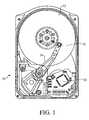
- FIG. 1is a plan view of a disk drive made in accordance with the present invention
- FIG. 2is a block diagram of the disk drive of FIG. 1 ;
- FIG. 3is a diagram of a portion of the disk in the drive of FIG. 1 ;
- FIG. 4Ais an illustration that describes error detection code generation using a cyclical redundancy check algorithm
- FIG. 4Bis an illustration that describes error detection code verification using a cyclical redundancy check algorithm
- FIG. 5Ais a diagram illustrating CRC generation performed on a 1 bit basis
- FIG. 5Bis a diagram illustrating CRC generation performed on an 8 bit basis
- FIG. 5Cis a diagram illustrating CRC generation performed on a 10 bit basis
- FIG. 6Ais an illustration describing data processing used by an error correction algorithm when writing data
- FIG. 6Bis an illustration describing the error correction process when reading data
- FIG. 7is a diagram showing how mask segments are identified for error correction purposes
- FIG. 8is a diagram describing a method by which data and CRC values can be corrected on the fly, without re-reading data
- FIG. 9is a diagram showing the process by which data is read from a disk and errors are detected, identified and corrected;
- FIG. 10is a flow chart describing the write process used by the disk drive of FIG. 1 ;
- FIG. 11is a flow chart describing the read process used by the disk drive of FIG. 1 ;
- FIG. 12is a diagram showing the CRC generation process based on a 10 bit symbol, used in the present invention.
- a typical magnetic disk drive 10includes a magnetic disk 12 , a spindle motor (not shown) that rotates the disk at a desired speed, and a head arm 14 that pivots to move a recording/reproducing head 18 back and forth across the disk as the disk rotates.
- the head 18can have a single head for both reading and writing, or separate heads for reading and writing.
- a controller 20is also provided.
- the magnetic disk drive 10could also be an optical or magneto-optical drive or the like, a tape drive or the like, or simply a communication system.
- the disk 12could be any suitable media, such as an optical or magneto-optical disk or the like, tape or the like, or a communication channel. These devices also have at least one head or the like, and a suitable controller.
- the head 18writes data to and reads data from the disk 12 with the general circuit configuration shown in FIG. 2 .
- the controller 20controls the reading and writing operations of the head 18 .
- the controller 20also provides data to the write head and receives data from the read head through a read channel 22 .
- the read channelprocesses the data on the basis of a predetermined symbol size, such as 10 bits.
- the controllerresponds to read and write commands from a host 24 , such as a PC or other computer.
- the host 24also sends data to the disk drive 10 through the controller 20 , and receives data from the disk drive 10 through the controller 20 .
- the host 24processes data on the basis of a different predetermined symbol size, such as one or two 8-bit bytes.
- a volatile staging memory 26such as a static dynamic random access memory (SDRAM) or any other suitable memory is operatively connected to the controller 20 .
- the staging memory 26processes data on the basis of the symbol size used by the host 24 , such as one or two bytes (8 or 16 bits).
- the controller 20stages the data in the memory 26 (see FIG. 4A ) and writes the data from the memory 26 to the disk 12 ( FIG. 4B ) as desired.
- the controller 20receives a read command from the host 24 , data that includes the requested data is read from the disk 12 as needed, and is assembled in the memory 26 ( FIG. 4A ). When the data is assembled, it is read from the memory 26 ( FIG. 4B ) and sent to the host 24 through the controller 20 .
- Datais stored on the disk 12 on circumferential tracks 30 , 31 , 32 , 33 , 34 etc., as seen in FIG. 3 .
- the datais organized in symbols (not shown) typically having 8 or 10 bits each.
- the symbolsare organized in sectors 35 , 36 , 37 , etc., which each typically include 4096 bits.
- the number of bits in a sectorcan vary for various reasons.
- the controller 20When data in a particular track and sector is requested, the controller 20 directs the head 18 to the desired sector, and typically reads the entire sector, even though the sector might or might not be full. Of course, during the writing operation, the controller 20 finds sectors that can accept data, and directs the write head to the proper track and sector, where the data is written to the disk. In FIG. 3 , the first sector in track 30 has a data error 38 , and the sector 37 has an error 39 .
- Errorscan be produced at any stage during the reading and writing processes.
- Several methods for detecting and/or correcting errors in the dataare available.
- One popular approach to error detection, without correction,is a cyclical redundancy check (CRC).
- CRCcyclical redundancy check
- CRC valuescheck bits
- FIG. 4ACRC values
- the controller 20 or other circuitis programmed to generate CRC values at a step 40 , typically a sector at a time, when the sector 42 is written to the SDRAM.
- the CRC algorithmgenerates a CRC value 44 for each sector. While the CRC value itself can be any size, a typical CRC value 44 has 32 bits.
- the CRC checking operationis shown in FIG. 4B .
- the sector 42 and CRC value 44are read from the SDRAM and processed through a CRC generation algorithm at step 40 .
- the CRC resultis compared with a constant or expected value at step 46 , and if the CRC result is the same as the constant, then the presence of errors is not detected, at a step 47 . If errors are found, the data is re-requested, at step 48 . If there are no CRC errors, the data is released to the disk or host, as commanded.
- the CRC algorithmcan operate on the basis of a variety of symbol sizes, such as the 1 bit, 8 bit and 10 bit symbol sizes described here as examples, as seen in FIGS. 5A , 5 B and 5 C.
- FIG. 5Aan initial 32 bit CRC check bit value is established for state 0 .
- a CRC calculationis made on bit 0 , generating a new CRC value in state 1 .
- the algorithmis executed on bit 1 , generating a CRC value in state 2 , etc., until a final CRC value is calculated in state 4096 . Since the CRC algorithm operates one bit at a time, each calculation takes one time unit to complete. Thus, in FIG. 5A , the CRC generation is complete after 4,096 time units.
- an initial 32 bit CRC valueis established in state 0 , but the algorithm is executed on 8 bits at a time, in a cascaded manner, so that the CRC algorithm is executed on the first 8 bits in one time unit.
- the algorithmis executed on 8 bits at a time, in a cascaded manner, so that the CRC algorithm is executed on the first 8 bits in one time unit.
- an initial 32 bit CRC valueis established in state 0 , and CRC values for the first 10 bits are calculated in a cascaded manner in a time unit 1 .
- CRC values for the first 10 bitsare calculated in a cascaded manner in a time unit 1 .
- the CRC valuecan be generated for the remaining 6 bits, one bit at a time, two bits at a time, etc., as desired.
- a popular method for error identification and correctionuses a relatively complex algorithm in which data strings are produced and stored on the disk with the data.
- the data stringsare commonly called error correction codes (ECCs). While the data strings could be any number of bits in length, typical error correction codes are generated by the controller 20 or other device by dividing the bits in a sector into 10 bit symbols, as seen in FIG. 6A .
- a 4,096 bit sector 50is divided into 10 bit symbols 0 , 1 , 2 , . . . 408 .
- 4090 bitsare divided into 409 symbols, and the last 6 bits are placed in a symbol 409 .
- a 4 bit pad(e.g., 0000) is added to that symbol to give it 10 bits.
- the controller 20uses a generally available algorithm at step 52 , to generate 10 bit ECC symbols 54 , including symbols 0 , 1 , . . . 39 , for example, or any other desirable number of symbols.
- the ECC symbols 54are recorded on the disk with the data in the sector 50 .
- the reading operationis illustrated in FIG. 6B .
- the sector 50 and ECC symbols 54are read from the disk, and an ECC calculation is performed by the controller 20 or other device at a step 55 .
- the ECC calculationuses the data and ECC symbols to determine whether there are errors. If errors are found in step 56 , the ECC symbols 54 are used to identify the data errors and correct them.
- the error locations and masksare identified in step 58 .
- the 10 bit symbol locations in the maskare correlated with the 8 bit symbol locations into which the data is organized at step 60 , and the data is corrected in the staging memory in step 62 using a read/modify/write process, as will be described.
- the errorsare corrected, the data values are correct in the SDRAM, and the ECC correction operation is finished at step 64 .
- the error/mask location data searchis shown in greater detail in FIG. 7 . Assuming 4,096 bits in a sector, with an error in data bit 66 , the data on the disk, organized in 10 bit ECC symbols, is shown in line 68 .
- the data organization schemeincludes the 10 bit symbols used for the ECC algorithm, including a 6 bit remainder and a 4 bit pad that completes the last symbol. The data bits are followed by the recorded ECC symbols.
- the same datais stored in the SDRAM, divided into 8 bit symbols, followed by the CRC value generated while writing the data from the disk to the SDRAM, as seen in line 70 .
- the SDRAM dataincludes the error 66 , and a CRC value 71 that correctly reflects the error 66 , but is considered erroneous in this context due to the error 66 .
- the CRC value 71 in this embodimentis a 32 bit value generated on the basis of an eight bit symbol.
- a maskis generated for each bit by the ECC algorithm, as seen in line 72 . If there are no errors, the ECC algorithm will record all zeros in this example. If there is an error, however, as at bit 66 , the mask will generate a one at bit 73 .
- the error 66can be easily corrected with the ECC algorithm. In fact, the bit 66 can be corrected without re-reading the data from the disk with this method, because the error is corrected through the ECC algorithm. In this manner, data errors are corrected on the fly.
- the erroneous CRC value 71must also be corrected.
- the erroneous CRC valuecould be corrected by re-reading the whole sector from SDRAM after the data correction process, but that is time consuming and inconvenient, as will be seen. For this reason, it is desirable to correct the erroneous CRC value 71 on the fly, as well.
- the erroneous CRC value 71can be corrected on the fly in the manner shown in FIG. 8 , as well as FIG. 7 .
- the data 68including the error 66 , is processed through a CRC algorithm at step 40 , generating the CRC value 71 while writing to the SDRAM.
- the CRC value 71is considered erroneous because it is calculated with the error 66 .
- the mask data 72 developed from the mask segment for data bytes 76 , 77includes the mask data bit 73 , corresponding to the erroneous data bit 66 .
- the mask segments in the mask dataare subjected to an XOR operation with the data bytes 76 and 77 (with the error 66 ), which corrects the error 66 in the data 68 , as seen in line 78 of FIG. 7 .
- the mask data 72is also passed through the CRC generator 40 , after the error is identified, and a mask CRC value 79 is generated.
- the CRC value 79is also a 32 bit value, but it is generated on the basis of 10 bit symbols, as will be explained.
- the error CRC 71is subjected to an XOR operation with the mask CRC 79 , generating a 32 bit corrected CRC value 80 , also seen in line 78 in FIG. 7 .
- the data 68 with the error 66 and the mask data 72are processed bit by bit through an XOR operation, creating data 78 that does not have errors.
- the erroneous CRC value 71 and the mask CRC 79are also processed bit by bit through an XOR operation, which generates the corrected CRC value 80 . In this manner, both the data error and the CRC error generated by that data error are corrected, without re-reading the data.
- Sectors 35 , 36 and 37are read sequentially from a selected track on the disk in step (a), starting at times t 1 , t 2 and t 5 , respectively, and the sectors read from the disk are written to the SDRAM or other memory 26 .
- the datais stored on the disk in a 10 bit symbol format, as previously described.
- step (b)As the data is read from the disk, it is converted to an 8 bit format in step (b), also starting at times t 1 , t 2 and t 5 . CRC values are generated in step (c) and the data is written to the memory 26 in step (d). The bit length conversion and CRC generation take very little time, so all three steps occur virtually simultaneously as data is read from the disk.
- the ECC calculationbegins in step (e) as each sector is read, starting at times t 1 , t 2 and t 5 , but that takes more time than the CRC generation (times t 3 , t 6 and t 8 , respectively) and cannot be completed before the next sector is read from the disk, because the disk rotates very quickly.
- sector 36is read from time t 2 , but the ECC calculations on sector 35 are not finished until time t 3 .
- step eIf an error is discovered during the ECC calculation for a sector such as sector 35 (step e), the error is identified using a search algorithm in step 35 (f) (starting at time t 3 ) based on the 10 bit ECC format, and the mask CRC value is generated at step (g) from the 10 bit ECC mask values identified in step (f). Step (f) and step (g) are performed in parallel. Then, the mask is converted to the 8 bit format in step (h). Finally, the data error and CRC value are corrected in the SDRAM in step (i), and those processes are completed at time t 4 . The data can then be read from the SDRAM in step (j).
- the CRCis checked as the data is sent to the host, and the process is completed if there are no errors. If there are errors, the data is re-requested from the disk. As seen in FIG. 9 , however, the correction in sector 35 is not completed before at least one other sector (sector 36 , for example) is at least partially read from the disk.
- the data error and CRC error in sector 35are corrected on the fly through the error search, CRC mask generation and error correction process, previously described during the time that sector 36 is read.
- error correction in steps (f), (g), (h) and (i)is not needed (N/A) and the data can be simply sent to the host in step (j) at time t 7 , following the completion of step (j) for sector 35 with the CRC check performed as previously described.
- Errors in sector 37are corrected in a manner similar to the manner in which the errors in sector 35 are corrected, from time t 5 to time t 9 .
- the write processis described in more detail in FIG. 10 .
- CRC codesare generated from the first bit length data in step 1012 , and the data is written to the SDRAM 26 with the CRC codes, in step 1014 (see FIG. 4A ).
- the first bit length datais read from the SDRAM 26 with the CRC codes at step 1016 .
- the CRC codesare checked (see FIG. 4B ), and if an error is discovered, the controller 20 returns to the host and has the data read again, stored in the SDRAM 26 , and then read from the SDRAM 26 at step 1018 .
- the datais processed by an error correction code algorithm in the controller 20 .
- the datais converted to the second bit length and a pad is added at step 1020 , and ECC codes are generated at step 1022 .
- the data (now organized according to the second bit length) and the ECC codes (which are based on the second bit length)are stored on the disk 12 at step 1024 .
- the write processis completed at step 1026 .
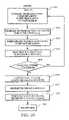
- the read processis described in more detail in FIG. 11 .
- the controllerreceives a read command, the controller identifies the sectors which must be read from the disk 12 to satisfy the command, and instructs the head 18 to read those sectors.
- the datais read with its related ECC codes at step 1110 , and is converted from second bit length symbol format to first bit length symbol format at step 1111 .
- a CRC valueis generated based on the first bit length at step 1112 , and the data and CRC value generated at step 1112 are written to the SDRAM 26 at step 1120 . This process is similarly described in connection with FIG. 4A .
- the datais processed using the ECC codes, based on the second bit length, at step 1114 . If errors are or are not found, subsequent processing is determined at step 1115 .
- the controllerreads the first bit length data and CRC value from the SDRAM at step 1122 , and checks the newly generated CRC value against the previously generated CRC value at step 1124 . This process is similarly described in connection with FIG. 4A .
- step 1124If no errors are found in step 1124 , the data is sent to the host 24 at step 1126 . If errors are found at step 1124 , the controller returns to step 1110 and re-reads the data, through step 1134 .
- an error searchoccurs at step 1128 .
- the CRC maskis generated based on the second bit length, as described earlier in connection with steps (f) and (g) in FIG. 9 . Further explanation of CRC generation based on the second bit length will be given in connection with FIG. 12 .
- the mask segmentsare mapped to corresponding first bit length symbols at step 1130 , as previously described.
- the data and CRC valuesare corrected in the manner previously described, at step 1132 .
- the first bit length data and CRC valueare read from the SDRAM 26 in step 1122 , and the process continues as previously described. In this manner, the data is read, modified and re-written to correct errors and calculate the CRC values.
- step 1118the controller determines whether no errors were detected (in step 1115 ), or whether errors were found and corrected (step 1132 ). If either answer is yes, the process continues to step 1122 . If not, the controller waits for a positive response from step 1115 or 1132 .
- CRC generation based on the second bit lengthwill now be described in greater detail. If the second bit length is not evenly divisible into the total number of bits, then a remainder will be left after all but the last bits are processed. For example, in the case of the first bit length data having 512 8-bit bytes, there are 4096 total bits. If the second bit length is 10 bits, then 4090 bits will be processed in 409 10 bit symbols. The remaining 6 bits will be processed on the following basis.
- the CRC generation process based on 10 bit symbolsis shown in FIG. 12 . Since the error correction code uses 10 bit symbols, then the CRC calculation is made for every 10 bit symbol until the remainder X is less than 10, at step 1210 , similar to FIG. 5C . By calculating the CRC value in this manner, the sector can be any desired size.
- the CRC for the remainderis calculated based on a “two-bit shift” or on the basis of single bit shifts, in step 1212 . Thus, if the remainder X is 4, 8, 2 or 6, the number of two-bit shifts required to process the remainder would be 2, 4, 1 and 3, respectively.
- a single 4-bit shift, a single 8-bit shift, a single 2-bit shift or a single 6-bit shiftcould be done for the remainder, if preferred.
- Another alternativeis to perform a suitable number of 1-bit shifts.
Landscapes
- Engineering & Computer Science (AREA)
- Physics & Mathematics (AREA)
- Probability & Statistics with Applications (AREA)
- Theoretical Computer Science (AREA)
- Signal Processing (AREA)
- Computing Systems (AREA)
- Detection And Correction Of Errors (AREA)
- Signal Processing For Digital Recording And Reproducing (AREA)
- Error Detection And Correction (AREA)
Abstract
Description
This invention relates to methods and apparatus for detecting and correcting data errors, and more particularly, to methods and apparatus for correcting data errors and data error detection codes such as cyclical redundancy check (CRC) values on the fly, without requiring re-reading of data.
In modern computer systems, data is constantly written to and read front several memory devices. One such device is a disk drive. While disk drives are used for permanent or non-volatile data storage on a magnetic or optical disk, they typically use internal volatile memory such as SDRAM to stage data before writing data to the disk. The SDRAM is also used to stage data after reading it from the disk, before it is sent to the host. However, every staging operation in the SDRAM creates an opportunity for error, both from the host to the disk and from the disk to the host. As a result, some method of error detection (and sometimes correction) must be employed every time data is transferred, even within the disk drive.
In the disk drives just described, when the data is received from the host and written to the staging memory, error detection capability is typically added. A relatively simple, low overhead algorithm such as Cyclical Redundancy Check (CRC) can determine whether there are any errors in the data. As the data is written to the staging memory, the CRC algorithm adds some check bits to the data that allow for detection of errors when the data is read at a later time. At a desired time, the data is read from the staging memory and sent to the disk.
As the data is read from the staging memory, the CRC algorithm reads the data and the check bits to determine whether there are any errors in the data. If there are errors, the data is re-requested from the host and the process is repeated, until the data is transferred to the disk without errors. The CRC algorithm need not correct errors, however, because if there are errors, the data can be re-requested from the host until the data transfer is successfully completed without errors. Thus, it is not necessary for the CRC algorithm to identify or correct errors at this stage. The CRC algorithm merely determines whether any errors exist in the data.
The data is also checked for errors when it is sent through the staging memory in the other direction, i.e., from the disk to the host. Thus, when the data is received from the disk and the data is written to the staging memory, the CRC algorithm adds CRC check bits to the data. When the data is read from the staging memory, the CRC algorithm checks the data and CRC bits to determine whether there are errors. In the case of an error, the data is re-requested from the disk and the operation repeats until the data is successfully transferred without errors.
Insuring the integrity of the data stored on the disk requires a more complex error correction algorithm. If the data stored on the disk has errors, the errors must be identified and corrected without rereading the data, because the errors are likely stored on the disk and the data is presumably not available from the host or another source. In this case, a more sophisticated algorithm must be used that can identify the errors and correct them.
Error identification and correction requires more complex, relatively high overhead algorithms. Such algorithms produce data strings, commonly called Error Correction Codes (ECCs), that are stored on the disk with the data. When the data is read from the disk, it is checked against the ECC's, and if errors are detected, most of the errors can be identified and corrected. Some ECC implementations use a Cyclical Redundancy Check algorithm that verifies that the errors have been corrected, as desired.
Data is generally written to and read out of the disk in sectors containing some number of bytes, such as 512 bytes, or 4096 bits. As the first sector is read from the disk, it is immediately written to the staging memory. At the same time, the ECC algorithm is executed, and a CRC value is calculated. If an error is found by the ECC algorithm, mask data is generated that specifies which bytes in the SDRAM should be corrected. Then, the erroneous bytes are read from the SDRAM and XORed with the mask data and written back to the SDRAM. The CRC mask is calculated using the mask data from the ECC algorithm. In this manner, the data and CRC value can be corrected without re-reading the whole sector from the SDRAM.
In the past, a typical disk drive used a single bit length or symbol length for data and for its ECC algorithm. Recently, however, ECC algorithms using 10 bit symbols have been adopted, even though the host still communicates in 8 bit symbols, the staging memories store data based on 8 bit symbols, and the CRC algorithm is also based on those 8 bit symbols. This is a problem because the mask segments created by the ECC algorithm do not directly correspond to or lie over the data bytes, so the CRC value cannot merely be calculated according to the ECC mask layout to complete the correction process.
The CRC values could be recalculated by re-reading the whole corrected sector from the SDRAM, but that process would be time consuming, and would slow the operation of the drive. Thus, there is a need for methods and apparatus for correcting data and error detection codes on the fly, without reading the data after it has been corrected.
Another problem encountered when the ECC algorithm processes the data in symbols having a different size than the symbols in which the data is organized is that if the ECC bit symbols cannot divide evenly into the number of bits in the sectors, the remainder is difficult to process. If the sector has 4,096 bits, for example, an algorithm that uses 10 bit symbols for processing purposes will process409 symbols, and have 6 bits remaining. The CRC calculation fails because it is based on 4090 bits or 4100 bits, not 4096 bits. Thus, there is a need for methods and apparatus for correcting the CRC calculations, irrespective of whether the symbol length of a correction algorithm is evenly divisible into the number of bits in a sector.
If a disk drive controller operates on the basis of a single sector size, the control can only be used for that sector size. This limits the flexibility of the controller. Thus, there is a need for methods and apparatus for detecting errors in data, regardless of the sector size.
In keeping with one aspect of this invention, data and error detection codes such as cyclical redundancy check (CRC) values (or check bits) are corrected on the fly, without slowing data reading operations. In a data reading operation, for example, a first sector is read from a disk and stored in volatile memory. Error detection values generated by a CRC algorithm are also stored in the volatile memory.
The data is organized in symbols each having some number of bits, and the CRC algorithm is executed on the basis of the symbol size of the data, to produce a CRC value having some number of bits. The stored CRC values can be used later to identify that errors have occurred, but the CRC algorithm cannot readily correct the errors. To correct errors, a more complex algorithm such as an ECC algorithm is executed.
The ECC algorithm is executed on the first sector while a second sector is being read from the disk, to speed operation of the drive. When errors are found, both the data and the CRC value indicating the errors are corrected, without re-reading the first sector, even if the data is organized in symbols having one bit length and the ECC algorithm operates on the basis of symbols having a different symbol size. In one embodiment, the ECC algorithm generates ECC mask data that identifies the locations of the erroneous data. The erroneous data is corrected by performing an exclusive OR (XOR) operation on the erroneous data segments and the mask data. A CRC mask value is also generated from the ECC mask. The CRC mask value has the same number of bits as the first CRC value, but this time the CRC algorithm is executed on the basis of the symbol size of the ECC algorithm. An XOR operation is performed on the CRC value obtained from the erroneous data and the CRC mask value obtained from the ECC mask, which produces a correct CRC value for the corrected data. The correct CRC values are then stored in the volatile memory with the corrected data. When the data is read from the SDRAM and sent to the host, the CRC algorithm uses the data and stored CRC value to validate that the data has no errors.
The above mentioned and other features of this invention and the manner of obtaining them will become more apparent, and the invention itself will be best understood by reference to the following description of an embodiment of the invention taken in conjunction with the accompanying drawings, in which:
As seen inFIG. 1 , a typicalmagnetic disk drive 10 includes amagnetic disk 12, a spindle motor (not shown) that rotates the disk at a desired speed, and ahead arm 14 that pivots to move a recording/reproducinghead 18 back and forth across the disk as the disk rotates. Thehead 18 can have a single head for both reading and writing, or separate heads for reading and writing. Acontroller 20 is also provided.
Themagnetic disk drive 10 could also be an optical or magneto-optical drive or the like, a tape drive or the like, or simply a communication system. Thedisk 12 could be any suitable media, such as an optical or magneto-optical disk or the like, tape or the like, or a communication channel. These devices also have at least one head or the like, and a suitable controller.
Thehead 18 writes data to and reads data from thedisk 12 with the general circuit configuration shown inFIG. 2 . Thecontroller 20 controls the reading and writing operations of thehead 18. Thecontroller 20 also provides data to the write head and receives data from the read head through aread channel 22. The read channel processes the data on the basis of a predetermined symbol size, such as 10 bits.
The controller responds to read and write commands from ahost 24, such as a PC or other computer. Thehost 24 also sends data to thedisk drive 10 through thecontroller 20, and receives data from thedisk drive 10 through thecontroller 20. However, thehost 24 processes data on the basis of a different predetermined symbol size, such as one or two 8-bit bytes.
In order to facilitate operations of thedisk drive 10, avolatile staging memory 26 such as a static dynamic random access memory (SDRAM) or any other suitable memory is operatively connected to thecontroller 20. The stagingmemory 26 processes data on the basis of the symbol size used by thehost 24, such as one or two bytes (8 or 16 bits). When data is received from thehost 24, thecontroller 20 stages the data in the memory26 (seeFIG. 4A ) and writes the data from thememory 26 to the disk12 (FIG. 4B ) as desired. When thecontroller 20 receives a read command from thehost 24, data that includes the requested data is read from thedisk 12 as needed, and is assembled in the memory26 (FIG. 4A ). When the data is assembled, it is read from the memory26 (FIG. 4B ) and sent to thehost 24 through thecontroller 20.
Data is stored on thedisk 12 oncircumferential tracks FIG. 3 . For data processing purposes, the data is organized in symbols (not shown) typically having 8 or 10 bits each. The symbols are organized insectors
When data in a particular track and sector is requested, thecontroller 20 directs thehead 18 to the desired sector, and typically reads the entire sector, even though the sector might or might not be full. Of course, during the writing operation, thecontroller 20 finds sectors that can accept data, and directs the write head to the proper track and sector, where the data is written to the disk. InFIG. 3 , the first sector intrack 30 has adata error 38, and thesector 37 has anerror 39.
Errors can be produced at any stage during the reading and writing processes. Several methods for detecting and/or correcting errors in the data are available. One popular approach to error detection, without correction, is a cyclical redundancy check (CRC). In the CRC method, CRC values (check bits) are generated in the manner illustrated inFIG. 4A , and the CRC values are checked in the manner shown inFIG. 4B .
Referring now toFIG. 2 andFIG. 4A , thecontroller 20 or other circuit is programmed to generate CRC values at astep 40, typically a sector at a time, when thesector 42 is written to the SDRAM. The CRC algorithm generates aCRC value 44 for each sector. While the CRC value itself can be any size, atypical CRC value 44 has 32 bits.
The CRC checking operation is shown inFIG. 4B . Thesector 42 andCRC value 44 are read from the SDRAM and processed through a CRC generation algorithm atstep 40. The CRC result is compared with a constant or expected value atstep 46, and if the CRC result is the same as the constant, then the presence of errors is not detected, at astep 47. If errors are found, the data is re-requested, atstep 48. If there are no CRC errors, the data is released to the disk or host, as commanded.
The CRC algorithm can operate on the basis of a variety of symbol sizes, such as the 1 bit, 8 bit and 10 bit symbol sizes described here as examples, as seen inFIGS. 5A ,5B and5C. InFIG. 5A , an initial 32 bit CRC check bit value is established forstate 0. A CRC calculation is made onbit 0, generating a new CRC value instate 1. The algorithm is executed onbit 1, generating a CRC value instate 2, etc., until a final CRC value is calculated instate 4096. Since the CRC algorithm operates one bit at a time, each calculation takes one time unit to complete. Thus, inFIG. 5A , the CRC generation is complete after 4,096 time units.
InFIG. 5B , an initial 32 bit CRC value is established instate 0, but the algorithm is executed on 8 bits at a time, in a cascaded manner, so that the CRC algorithm is executed on the first 8 bits in one time unit. By executing the algorithm in 8 bit segments, only 512 time units are required to process the 4,096 bits.
InFIG. 5C , an initial 32 bit CRC value is established instate 0, and CRC values for the first 10 bits are calculated in a cascaded manner in atime unit 1. By cascading the calculations in units of 10 bits, only 409 time units are required to calculate a CRC value for 4,090 bits. The CRC value can be generated for the remaining 6 bits, one bit at a time, two bits at a time, etc., as desired.
A popular method for error identification and correction uses a relatively complex algorithm in which data strings are produced and stored on the disk with the data. The data strings are commonly called error correction codes (ECCs). While the data strings could be any number of bits in length, typical error correction codes are generated by thecontroller 20 or other device by dividing the bits in a sector into 10 bit symbols, as seen inFIG. 6A . A 4,096bit sector 50 is divided into 10bit symbols symbol 409. A 4 bit pad (e.g., 0000) is added to that symbol to give it 10 bits.
Before or as the data is written to thedisk 12, thecontroller 20 uses a generally available algorithm atstep 52, to generate 10bit ECC symbols 54, includingsymbols ECC symbols 54 are recorded on the disk with the data in thesector 50.
The reading operation is illustrated inFIG. 6B . Thesector 50 andECC symbols 54 are read from the disk, and an ECC calculation is performed by thecontroller 20 or other device at astep 55. The ECC calculation uses the data and ECC symbols to determine whether there are errors. If errors are found instep 56, theECC symbols 54 are used to identify the data errors and correct them. The error locations and masks are identified instep 58. The 10 bit symbol locations in the mask are correlated with the 8 bit symbol locations into which the data is organized atstep 60, and the data is corrected in the staging memory instep 62 using a read/modify/write process, as will be described. When the errors are corrected, the data values are correct in the SDRAM, and the ECC correction operation is finished atstep 64.
The error/mask location data search is shown in greater detail inFIG. 7 . Assuming 4,096 bits in a sector, with an error indata bit 66, the data on the disk, organized in 10 bit ECC symbols, is shown inline 68. The data organization scheme includes the 10 bit symbols used for the ECC algorithm, including a 6 bit remainder and a 4 bit pad that completes the last symbol. The data bits are followed by the recorded ECC symbols.
The same data is stored in the SDRAM, divided into 8 bit symbols, followed by the CRC value generated while writing the data from the disk to the SDRAM, as seen inline 70. The SDRAM data includes theerror 66, and aCRC value 71 that correctly reflects theerror 66, but is considered erroneous in this context due to theerror 66. TheCRC value 71 in this embodiment is a 32 bit value generated on the basis of an eight bit symbol.
From the data and ECC symbols inline 68, a mask is generated for each bit by the ECC algorithm, as seen inline 72. If there are no errors, the ECC algorithm will record all zeros in this example. If there is an error, however, as atbit 66, the mask will generate a one atbit 73.
Theerror 66 can be easily corrected with the ECC algorithm. In fact, thebit 66 can be corrected without re-reading the data from the disk with this method, because the error is corrected through the ECC algorithm. In this manner, data errors are corrected on the fly.
Theerroneous CRC value 71 must also be corrected. The erroneous CRC value could be corrected by re-reading the whole sector from SDRAM after the data correction process, but that is time consuming and inconvenient, as will be seen. For this reason, it is desirable to correct theerroneous CRC value 71 on the fly, as well.
Theerroneous CRC value 71 can be corrected on the fly in the manner shown inFIG. 8 , as well asFIG. 7 . Thedata 68, including theerror 66, is processed through a CRC algorithm atstep 40, generating theCRC value 71 while writing to the SDRAM. TheCRC value 71 is considered erroneous because it is calculated with theerror 66.
Themask data 72 developed from the mask segment fordata bytes mask data bit 73, corresponding to theerroneous data bit 66. The mask segments in the mask data are subjected to an XOR operation with the data bytes76 and77 (with the error66), which corrects theerror 66 in thedata 68, as seen inline 78 ofFIG. 7 .
Themask data 72 is also passed through theCRC generator 40, after the error is identified, and amask CRC value 79 is generated. TheCRC value 79 is also a 32 bit value, but it is generated on the basis of 10 bit symbols, as will be explained. Theerror CRC 71 is subjected to an XOR operation with themask CRC 79, generating a 32 bit correctedCRC value 80, also seen inline 78 inFIG. 7 .
Referring now toFIG. 8 , thedata 68 with theerror 66 and themask data 72 are processed bit by bit through an XOR operation, creatingdata 78 that does not have errors. Theerroneous CRC value 71 and themask CRC 79 are also processed bit by bit through an XOR operation, which generates the correctedCRC value 80. In this manner, both the data error and the CRC error generated by that data error are corrected, without re-reading the data.
The importance of correcting the CRC value and data on the fly can be better understood with reference toFIG. 9 .
As the data is read from the disk, it is converted to an 8 bit format in step (b), also starting at times t1, t2 and t5. CRC values are generated in step (c) and the data is written to thememory 26 in step (d). The bit length conversion and CRC generation take very little time, so all three steps occur virtually simultaneously as data is read from the disk.
The ECC calculation begins in step (e) as each sector is read, starting at times t1, t2 and t5, but that takes more time than the CRC generation (times t3, t6 and t8, respectively) and cannot be completed before the next sector is read from the disk, because the disk rotates very quickly. Thus, for example,sector 36 is read from time t2, but the ECC calculations onsector 35 are not finished until time t3. If an error is discovered during the ECC calculation for a sector such as sector35 (step e), the error is identified using a search algorithm in step35 (f) (starting at time t3) based on the 10 bit ECC format, and the mask CRC value is generated at step (g) from the 10 bit ECC mask values identified in step (f). Step (f) and step (g) are performed in parallel. Then, the mask is converted to the 8 bit format in step (h). Finally, the data error and CRC value are corrected in the SDRAM in step (i), and those processes are completed at time t4. The data can then be read from the SDRAM in step (j).
The CRC is checked as the data is sent to the host, and the process is completed if there are no errors. If there are errors, the data is re-requested from the disk. As seen inFIG. 9 , however, the correction insector 35 is not completed before at least one other sector (sector 36, for example) is at least partially read from the disk.
The data error and CRC error insector 35 are corrected on the fly through the error search, CRC mask generation and error correction process, previously described during the time thatsector 36 is read. Of course, if there are no errors, as withsector 36 inFIG. 9 , error correction in steps (f), (g), (h) and (i) is not needed (N/A) and the data can be simply sent to the host in step (j) at time t7, following the completion of step (j) forsector 35 with the CRC check performed as previously described. Errors insector 37 are corrected in a manner similar to the manner in which the errors insector 35 are corrected, from time t5 to time t9.
The value of correcting errors on the fly, without re-reading data, can now be better understood. Ifsector 35 had to be re-read from the SDRAM to recalculate the CRC value, the entire process would slow down.
The write process is described in more detail inFIG. 10 . When thehost 24 issues a write command to thecontroller 20 instep 1010, CRC codes are generated from the first bit length data instep 1012, and the data is written to theSDRAM 26 with the CRC codes, in step1014 (seeFIG. 4A ). The first bit length data is read from theSDRAM 26 with the CRC codes atstep 1016. As the data is read from theSDRAM 26, the CRC codes are checked (seeFIG. 4B ), and if an error is discovered, thecontroller 20 returns to the host and has the data read again, stored in theSDRAM 26, and then read from theSDRAM 26 atstep 1018.
If no data errors are identified, the data is processed by an error correction code algorithm in thecontroller 20. The data is converted to the second bit length and a pad is added atstep 1020, and ECC codes are generated atstep 1022. The data (now organized according to the second bit length) and the ECC codes (which are based on the second bit length) are stored on thedisk 12 atstep 1024. The write process is completed atstep 1026.
The read process is described in more detail inFIG. 11 . When the controller receives a read command, the controller identifies the sectors which must be read from thedisk 12 to satisfy the command, and instructs thehead 18 to read those sectors. The data is read with its related ECC codes atstep 1110, and is converted from second bit length symbol format to first bit length symbol format atstep 1111. A CRC value is generated based on the first bit length atstep 1112, and the data and CRC value generated atstep 1112 are written to theSDRAM 26 atstep 1120. This process is similarly described in connection withFIG. 4A .
In the same time frame, the data is processed using the ECC codes, based on the second bit length, atstep 1114. If errors are or are not found, subsequent processing is determined atstep 1115.
If no errors are found by the ECC algorithm atstep 1115, the controller reads the first bit length data and CRC value from the SDRAM atstep 1122, and checks the newly generated CRC value against the previously generated CRC value atstep 1124. This process is similarly described in connection withFIG. 4A .
If no errors are found instep 1124, the data is sent to thehost 24 atstep 1126. If errors are found atstep 1124, the controller returns to step1110 and re-reads the data, throughstep 1134.
If one or more errors are found atstep 1115, an error search occurs atstep 1128. During this search, the CRC mask is generated based on the second bit length, as described earlier in connection with steps (f) and (g) inFIG. 9 . Further explanation of CRC generation based on the second bit length will be given in connection withFIG. 12 . Once the mask locations are known, the mask segments are mapped to corresponding first bit length symbols atstep 1130, as previously described. The data and CRC values are corrected in the manner previously described, atstep 1132. The first bit length data and CRC value are read from theSDRAM 26 instep 1122, and the process continues as previously described. In this manner, the data is read, modified and re-written to correct errors and calculate the CRC values.
Instep 1118, the controller determines whether no errors were detected (in step1115), or whether errors were found and corrected (step1132). If either answer is yes, the process continues to step1122. If not, the controller waits for a positive response fromstep
CRC generation based on the second bit length will now be described in greater detail. If the second bit length is not evenly divisible into the total number of bits, then a remainder will be left after all but the last bits are processed. For example, in the case of the first bit length data having 512 8-bit bytes, there are 4096 total bits. If the second bit length is 10 bits, then 4090 bits will be processed in 409 10 bit symbols. The remaining 6 bits will be processed on the following basis.
The CRC generation process based on 10 bit symbols is shown inFIG. 12 . Since the error correction code uses 10 bit symbols, then the CRC calculation is made for every 10 bit symbol until the remainder X is less than 10, atstep 1210, similar toFIG. 5C . By calculating the CRC value in this manner, the sector can be any desired size. The CRC for the remainder is calculated based on a “two-bit shift” or on the basis of single bit shifts, instep 1212. Thus, if the remainder X is 4, 8, 2 or 6, the number of two-bit shifts required to process the remainder would be 2, 4, 1 and 3, respectively. In the alternative, a single 4-bit shift, a single 8-bit shift, a single 2-bit shift or a single 6-bit shift could be done for the remainder, if preferred. Another alternative is to perform a suitable number of 1-bit shifts.
While the principles of the invention have been described above in connection with specific apparatus and applications, it is to be understood that this description is made only by way of example and not as a limitation on the scope of the invention.
Claims (12)
1. A method for reading data from a non-volatile data storage medium, the data being organized in sectors having some predetermined number of bits, comprising the steps of:
reading a sector from the medium and storing the sector data in volatile memory,
using a first algorithm, operated on the basis of a first bit length, to generate check bits based on the sector data, the check bits being stored in the volatile memory, and
detecting and identifying at least some errors in the data using a second algorithm that operates on the basis of symbols having a second bit length,
wherein the data and check bits stored in the volatile memory do not change if no errors are found, but if errors are found,
using the second algorithm to correct the data stored in the volatile memory, and
using the first algorithm, operated on the basis of the second bit length, to correct the check bits stored in the volatile memory to reflect the error corrections,
thus not requiring re-reading the sector from the volatile memory to correct the check bits stored in the volatile memory.
2. The method ofclaim 1 wherein selected sectors are read from the medium successively.
3. The method ofclaim 1 wherein the check bits are corrected without re-reading the sector by,
generating a mask using the second algorithm, the mask including mask segments that include the erroneous data,
executing the first algorithm on the mask segments, operated on the basis of the second bit length, and
performing an XOR operation on the check bits calculated using the first algorithm operated on the basis of the first bit length, and the check bits generated by the first algorithm from the mask data,
whereby correct check bits are stored in the volatile memory.
4. The method ofclaim 1 , wherein if the total number of bits is not evenly divisible by the second bit length, when the first algorithm is operated on the basis of the second bit length, a check bit calculation is made for every symbol until the remainder is less than the second bit length, CRC check bits then being calculated for the remainder based on a predetermined number of 2-bit shifts.
5. The method ofclaim 1 , wherein if the total number of bits is not evenly divisible by the second bit length, when the first algorithm is operated on the basis of the second bit length, a check bit calculation is made for every symbol until the remainder is less than the second bit length, CRC check bits then being calculated for the remainder based on a single multi-bit shift.
6. The method ofclaim 1 , wherein if the total number of bits is not evenly divisible by the second bit length, when the first algorithm is operated on the basis of the second bit length, a check bit calculation is made for every symbol until the remainder is less than the second bit length, CRC check bits then being calculated for the remainder based on a predetermined number of 1-bit shifts.
7. A magnetic disk drive comprising:
a magnetic disk,
at least one head for writing and reading data from and to the disk,
a controller for sending and receiving data to and from a host, and
a volatile staging memory for writing and reading data to and from the host, and to and from the disk, under the control of the controller,
the data being organized in sectors each having some predetermined number of bits,
the data being stored in the volatile staging memory as it is read from the disk,
the controller using a first algorithm, operated on the basis of a first bit length, to generate check bits based on the sector data, the check bits being stored in the volatile memory,
the controller detecting and identifying errors in the data using a second algorithm that operates on the basis of symbols having a second bit length,
wherein the data stored in the volatile staging memory is sent to the host by the controller if no errors are found, but if errors are found,
the controller uses the second algorithm to correct the data stored in the volatile storage staging memory, and
the controller uses the first algorithm, operated on the basis of the second bit length, to correct the check bits stored in the volatile memory to reflect the error corrections,
thus not requiring re-reading the sector from the volatile staging memory to correct the check bits stored in the volatile staging memory.
8. The apparatus ofclaim 7 wherein selected sectors are read from the disk successively.
9. The apparatus ofclaim 7 wherein the controller includes,
means for generating a mask using the second algorithm, the mask including mask segments that include the erroneous data,
executing the first algorithm on the mask segments, operated on the basis of the second bit length, and
performing an XOR operation on the check bits calculated using the first algorithm operated on the basis of the first bit length, and the check bits generated by the first algorithm from the mask data,
whereby correct check bits are stored in the volatile memory.
10. The apparatus ofclaim 7 , wherein if the total number of bits is not evenly divisible by the second bit length, when the first algorithm is operated on the basis of the second bit length, a check bit calculation is made for every symbol until the remainder is less than the second bit length, CRC check bits then being calculated for the remainder based on a predetermined number of 2-bit shifts.
11. The apparatus ofclaim 7 , wherein if the total number of bits is not evenly divisible by the second bit length, when the first algorithm is operated on the basis of the second bit length, a check bit calculation is made for every symbol until the remainder is less than the second bit length, CRC check bits then being calculated for the remainder based on a single multi-bit shift.
12. The apparatus ofclaim 7 , wherein if the total number of bits is not evenly divisible by the second bit length, when the first algorithm is operated on the basis of the second bit length, a check bit calculation is made for every symbol until the remainder is less than the second bit length, CRC check bits then being calculated for the remainder based on a predetermined number of 1-bit shifts.
Priority Applications (1)
| Application Number | Priority Date | Filing Date | Title |
|---|---|---|---|
| US10/452,603US7191382B2 (en) | 2003-06-02 | 2003-06-02 | Methods and apparatus for correcting data and error detection codes on the fly |
Applications Claiming Priority (1)
| Application Number | Priority Date | Filing Date | Title |
|---|---|---|---|
| US10/452,603US7191382B2 (en) | 2003-06-02 | 2003-06-02 | Methods and apparatus for correcting data and error detection codes on the fly |
Publications (2)
| Publication Number | Publication Date |
|---|---|
| US20040243885A1 US20040243885A1 (en) | 2004-12-02 |
| US7191382B2true US7191382B2 (en) | 2007-03-13 |
Family
ID=33452031
Family Applications (1)
| Application Number | Title | Priority Date | Filing Date |
|---|---|---|---|
| US10/452,603Expired - Fee RelatedUS7191382B2 (en) | 2003-06-02 | 2003-06-02 | Methods and apparatus for correcting data and error detection codes on the fly |
Country Status (1)
| Country | Link |
|---|---|
| US (1) | US7191382B2 (en) |
Cited By (59)
| Publication number | Priority date | Publication date | Assignee | Title |
|---|---|---|---|---|
| US20050055622A1 (en)* | 2003-09-05 | 2005-03-10 | Yuichiro Tsukamizu | Device and method for generating error correction code |
| US20080074778A1 (en)* | 2006-09-22 | 2008-03-27 | Agere Systems Inc. | Systems and Methods for Improving Disk Drive Synchronization |
| US20080184093A1 (en)* | 2007-01-26 | 2008-07-31 | Thayer Larry J | Error correction algorithm selection based upon memory organization |
| US20090002020A1 (en)* | 2007-06-27 | 2009-01-01 | Brad Hutchings | Dynamically tracking data values in a configurable ic |
| US20090052602A1 (en)* | 2007-08-20 | 2009-02-26 | Agere Systems Inc. | Systems and Methods for Improved Timing Recovery |
| US20090052075A1 (en)* | 2007-08-20 | 2009-02-26 | Agere Systems Inc. | Systems and Methods for Improved Synchronization Between an Asynchronously Detected Signal and a Synchronous Operation |
| US20090183056A1 (en)* | 2008-01-16 | 2009-07-16 | Bluearc Uk Limited | Validating Objects in a Data Storage system |
| US20090268322A1 (en)* | 2008-04-29 | 2009-10-29 | Agere Systems Inc. | Systems and Methods for Acquiring Modified Rate Burst Demodulation in Servo Systems |
| US20090267819A1 (en)* | 2008-04-29 | 2009-10-29 | Agere Systems Inc. | Systems and Methods for Reducing the Effects of ADC Mismatch |
| US20090323214A1 (en)* | 2008-06-27 | 2009-12-31 | Agere Systems Inc. | Modulated Disk Lock Clock and Methods for Using Such |
| US20100067628A1 (en)* | 2008-09-17 | 2010-03-18 | Lsi Corporation | Adaptive Pattern Dependent Noise Prediction on a Feed Forward Noise Estimate |
| US20100177430A1 (en)* | 2007-12-14 | 2010-07-15 | George Mathew | Systems and Methods for Fly-Height Control Using Servo Address Mark Data |
| US20100202082A1 (en)* | 2008-07-28 | 2010-08-12 | Nils Graef | Systems and Methods for Variable Fly Height Measurement |
| US20100208377A1 (en)* | 2007-10-30 | 2010-08-19 | Grundvig Jeffrey P | Systems and Methods for Inter-Location Control of Storage Access |
| US20100232046A1 (en)* | 2006-05-01 | 2010-09-16 | Agere Systems Inc. | Methods and Systems for Estimating Time Corresponding to Peak Signal Amplitude |
| US20110002211A1 (en)* | 2009-07-02 | 2011-01-06 | Lsi Corporation | Systems and Methods for Format Efficient Timing Recovery In a Read Channel |
| US20110043938A1 (en)* | 2007-12-14 | 2011-02-24 | George Mathew | Systems and Methods for Fly-Height Control Using Servo Data |
| US20110099461A1 (en)* | 2009-10-22 | 2011-04-28 | Microsoft Corporation | Data integrity units in nonvolatile memory |
| US20110157737A1 (en)* | 2009-12-31 | 2011-06-30 | Lsi Corporation | Systems and Methods for Detecting a Reference Pattern |
| US8014099B2 (en) | 2007-12-14 | 2011-09-06 | Lsi Corporation | Systems and methods for using an on-the-fly CBD estimate to adjust fly-height |
| US8154972B2 (en) | 2009-06-24 | 2012-04-10 | Lsi Corporation | Systems and methods for hard disk drive data storage including reduced latency loop recovery |
| US8237597B2 (en) | 2010-09-21 | 2012-08-07 | Lsi Corporation | Systems and methods for semi-independent loop processing |
| US8243381B2 (en) | 2008-11-13 | 2012-08-14 | Agere Systems Inc. | Systems and methods for sector address mark detection |
| US8261171B2 (en) | 2011-01-27 | 2012-09-04 | Lsi Corporation | Systems and methods for diversity combined data detection |
| US8307271B1 (en)* | 2009-09-17 | 2012-11-06 | Emc Corporation | Fast verification of data block cycle redundancy checks |
| US8325433B2 (en) | 2011-01-19 | 2012-12-04 | Lsi Corporation | Systems and methods for reduced format data processing |
| US8411383B2 (en) | 2009-07-22 | 2013-04-02 | Lsi Corporation | Systems and methods for high order asymmetry correction |
| US8411385B2 (en) | 2010-12-20 | 2013-04-02 | Lsi Corporation | Systems and methods for improved timing recovery |
| US8498072B2 (en) | 2010-11-29 | 2013-07-30 | Lsi Corporation | Systems and methods for spiral waveform detection |
| US8498071B2 (en) | 2011-06-30 | 2013-07-30 | Lsi Corporation | Systems and methods for inter-track alignment |
| US8526131B2 (en) | 2010-11-29 | 2013-09-03 | Lsi Corporation | Systems and methods for signal polarity determination |
| US8566378B2 (en) | 2010-09-30 | 2013-10-22 | Lsi Corporation | Systems and methods for retry sync mark detection |
| US8565047B2 (en) | 2011-04-28 | 2013-10-22 | Lsi Corporation | Systems and methods for data write loopback based timing control |
| US8566381B2 (en) | 2010-08-05 | 2013-10-22 | Lsi Corporation | Systems and methods for sequence detection in data processing |
| US8564897B1 (en) | 2012-06-21 | 2013-10-22 | Lsi Corporation | Systems and methods for enhanced sync mark detection |
| US8614858B2 (en) | 2010-11-15 | 2013-12-24 | Lsi Corporation | Systems and methods for sync mark detection metric computation |
| US8625216B2 (en) | 2012-06-07 | 2014-01-07 | Lsi Corporation | Servo zone detector |
| US8665544B2 (en) | 2011-05-03 | 2014-03-04 | Lsi Corporation | Systems and methods for servo data detection |
| US8669891B2 (en) | 2011-07-19 | 2014-03-11 | Lsi Corporation | Systems and methods for ADC based timing and gain control |
| US8681444B2 (en) | 2012-06-07 | 2014-03-25 | Lsi Corporation | Multi-zone servo processor |
| US8705673B2 (en) | 2008-09-05 | 2014-04-22 | Lsi Corporation | Timing phase detection using a matched filter set |
| US8749908B2 (en) | 2011-03-17 | 2014-06-10 | Lsi Corporation | Systems and methods for sync mark detection |
| US8773811B2 (en) | 2011-12-12 | 2014-07-08 | Lsi Corporation | Systems and methods for zone servo timing gain recovery |
| US8780476B2 (en) | 2011-09-23 | 2014-07-15 | Lsi Corporation | Systems and methods for controlled wedge spacing in a storage device |
| US8874410B2 (en) | 2011-05-23 | 2014-10-28 | Lsi Corporation | Systems and methods for pattern detection |
| US8949701B2 (en) | 2008-09-23 | 2015-02-03 | Agere Systems Inc. | Systems and methods for low latency media defect detection |
| US8976475B1 (en) | 2013-11-12 | 2015-03-10 | Lsi Corporation | Systems and methods for large sector dynamic format insertion |
| US9019641B2 (en) | 2012-12-13 | 2015-04-28 | Lsi Corporation | Systems and methods for adaptive threshold pattern detection |
| US9053217B2 (en) | 2013-02-17 | 2015-06-09 | Lsi Corporation | Ratio-adjustable sync mark detection system |
| US9129650B2 (en) | 2013-07-25 | 2015-09-08 | Avago Technologies General Ip (Singapore) Pte. Ltd. | Array-reader based magnetic recording systems with frequency division multiplexing |
| US9129646B2 (en) | 2013-09-07 | 2015-09-08 | Avago Technologies General Ip (Singapore) Pte. Ltd. | Array-reader based magnetic recording systems with mixed synchronization |
| US9196297B2 (en) | 2013-03-14 | 2015-11-24 | Avago Technologies General Ip (Singapore) Pte. Ltd. | Systems and methods for enhanced sync mark mis-detection protection |
| US9224420B1 (en) | 2014-10-02 | 2015-12-29 | Avago Technologies General Ip (Singapore) Pte. Ltd. | Syncmark detection failure recovery system |
| US9275655B2 (en) | 2013-06-11 | 2016-03-01 | Avago Technologies General Ip (Singapore) Pte. Ltd. | Timing error detector with diversity loop detector decision feedback |
| US9305581B2 (en) | 2008-12-04 | 2016-04-05 | Avago Technologies General Ip (Singapore) Pte. Ltd. | Systems and methods for memory efficient repeatable run out processing |
| US20160117221A1 (en)* | 2014-10-22 | 2016-04-28 | Advanced Miro Devices, Inc. | Error detection and correction utilizing locally stored parity information |
| US9600363B2 (en) | 2015-04-24 | 2017-03-21 | Phison Electronics Corp. | Data accessing method, memory controlling circuit unit and memory storage apparatus |
| US9767120B2 (en) | 2008-01-16 | 2017-09-19 | Hitachi Data Systems Engineering UK Limited | Multi-way checkpoints in a data storage system |
| US10152999B2 (en) | 2013-07-03 | 2018-12-11 | Avago Technologies International Sales Pte. Limited | Systems and methods for correlation based data alignment |
Families Citing this family (11)
| Publication number | Priority date | Publication date | Assignee | Title |
|---|---|---|---|---|
| US7664987B2 (en)* | 2003-05-25 | 2010-02-16 | Sandisk Il Ltd. | Flash memory device with fast reading rate |
| US7409623B2 (en)* | 2004-11-04 | 2008-08-05 | Sigmatel, Inc. | System and method of reading non-volatile computer memory |
| US8504897B2 (en)* | 2007-06-21 | 2013-08-06 | Megachips Corporation | Memory controller |
| JP2010123156A (en)* | 2008-11-17 | 2010-06-03 | Elpida Memory Inc | Semiconductor storage device and control method thereof |
| US8352835B2 (en)* | 2009-06-10 | 2013-01-08 | International Business Machines Corporation | Data verification using checksum sidefile |
| WO2010150386A1 (en) | 2009-06-25 | 2010-12-29 | トヨタ自動車株式会社 | Hybrid vehicle structure |
| CN102612173B (en)* | 2011-01-21 | 2016-08-10 | 芯讯通无线科技(上海)有限公司 | The means of communication between multi mode terminal and communication module thereof |
| US8468423B2 (en) | 2011-09-01 | 2013-06-18 | International Business Machines Corporation | Data verification using checksum sidefile |
| CN105280240B (en)* | 2015-11-18 | 2018-02-13 | 致象尔微电子科技(上海)有限公司 | A kind of read method of Nand Flash parameters |
| CN110888750B (en)* | 2018-09-07 | 2024-07-05 | 阿里巴巴集团控股有限公司 | Data processing method and device |
| CN111752747A (en)* | 2020-06-09 | 2020-10-09 | 山东华翼微电子技术股份有限公司 | A memory security check method with enhanced error detection capability |
Citations (4)
| Publication number | Priority date | Publication date | Assignee | Title |
|---|---|---|---|---|
| US5459742A (en)* | 1992-06-11 | 1995-10-17 | Quantum Corporation | Solid state disk memory using storage devices with defects |
| US5691994A (en)* | 1995-05-08 | 1997-11-25 | Western Digital Corporation | Disk drive with fast error correction validation |
| US5696775A (en)* | 1994-09-23 | 1997-12-09 | Cirrus Logic, Inc. | Method and apparatus for detecting the transfer of a wrong sector |
| US6048090A (en)* | 1997-04-23 | 2000-04-11 | Cirrus Logic, Inc. | Error correction and concurrent verification of a product code |
- 2003
- 2003-06-02USUS10/452,603patent/US7191382B2/ennot_activeExpired - Fee Related
Patent Citations (4)
| Publication number | Priority date | Publication date | Assignee | Title |
|---|---|---|---|---|
| US5459742A (en)* | 1992-06-11 | 1995-10-17 | Quantum Corporation | Solid state disk memory using storage devices with defects |
| US5696775A (en)* | 1994-09-23 | 1997-12-09 | Cirrus Logic, Inc. | Method and apparatus for detecting the transfer of a wrong sector |
| US5691994A (en)* | 1995-05-08 | 1997-11-25 | Western Digital Corporation | Disk drive with fast error correction validation |
| US6048090A (en)* | 1997-04-23 | 2000-04-11 | Cirrus Logic, Inc. | Error correction and concurrent verification of a product code |
Cited By (78)
| Publication number | Priority date | Publication date | Assignee | Title |
|---|---|---|---|---|
| US20050055622A1 (en)* | 2003-09-05 | 2005-03-10 | Yuichiro Tsukamizu | Device and method for generating error correction code |
| US8059349B2 (en) | 2006-05-01 | 2011-11-15 | Agere Systems Inc. | Methods and systems for estimating time corresponding to peak signal amplitude |
| US20100232046A1 (en)* | 2006-05-01 | 2010-09-16 | Agere Systems Inc. | Methods and Systems for Estimating Time Corresponding to Peak Signal Amplitude |
| US20080074778A1 (en)* | 2006-09-22 | 2008-03-27 | Agere Systems Inc. | Systems and Methods for Improving Disk Drive Synchronization |
| US7499238B2 (en)* | 2006-09-22 | 2009-03-03 | Agere Systems Inc. | Systems and methods for improving disk drive synchronization |
| US20080184093A1 (en)* | 2007-01-26 | 2008-07-31 | Thayer Larry J | Error correction algorithm selection based upon memory organization |
| US7975205B2 (en)* | 2007-01-26 | 2011-07-05 | Hewlett-Packard Development Company, L.P. | Error correction algorithm selection based upon memory organization |
| US20090002020A1 (en)* | 2007-06-27 | 2009-01-01 | Brad Hutchings | Dynamically tracking data values in a configurable ic |
| US20090052602A1 (en)* | 2007-08-20 | 2009-02-26 | Agere Systems Inc. | Systems and Methods for Improved Timing Recovery |
| US20090052075A1 (en)* | 2007-08-20 | 2009-02-26 | Agere Systems Inc. | Systems and Methods for Improved Synchronization Between an Asynchronously Detected Signal and a Synchronous Operation |
| US8054931B2 (en) | 2007-08-20 | 2011-11-08 | Agere Systems Inc. | Systems and methods for improved timing recovery |
| US8254049B2 (en) | 2007-08-20 | 2012-08-28 | Agere Systems Inc. | Systems and methods for improved synchronization between an asynchronously detected signal and a synchronous operation |
| US8174784B2 (en) | 2007-10-30 | 2012-05-08 | Agere Systems Inc. | Systems and methods for inter-location control of storage access |
| US20100208377A1 (en)* | 2007-10-30 | 2010-08-19 | Grundvig Jeffrey P | Systems and Methods for Inter-Location Control of Storage Access |
| US20100177430A1 (en)* | 2007-12-14 | 2010-07-15 | George Mathew | Systems and Methods for Fly-Height Control Using Servo Address Mark Data |
| US8054573B2 (en) | 2007-12-14 | 2011-11-08 | Lsi Corporation | Systems and methods for fly-height control using servo address mark data |
| US8154818B2 (en) | 2007-12-14 | 2012-04-10 | Lsi Corporation | Systems and methods for adaptive CBD estimation in a storage device |
| US9305582B2 (en) | 2007-12-14 | 2016-04-05 | Avago Technologies General Ip (Singapore) Pte. Ltd. | Systems and methods for fly-height control using servo data |
| US8014099B2 (en) | 2007-12-14 | 2011-09-06 | Lsi Corporation | Systems and methods for using an on-the-fly CBD estimate to adjust fly-height |
| US20110043938A1 (en)* | 2007-12-14 | 2011-02-24 | George Mathew | Systems and Methods for Fly-Height Control Using Servo Data |
| US9767120B2 (en) | 2008-01-16 | 2017-09-19 | Hitachi Data Systems Engineering UK Limited | Multi-way checkpoints in a data storage system |
| US8504904B2 (en)* | 2008-01-16 | 2013-08-06 | Hitachi Data Systems Engineering UK Limited | Validating objects in a data storage system |
| US20090183056A1 (en)* | 2008-01-16 | 2009-07-16 | Bluearc Uk Limited | Validating Objects in a Data Storage system |
| US7813065B2 (en) | 2008-04-29 | 2010-10-12 | Agere Systems Inc. | Systems and methods for acquiring modified rate burst demodulation in servo systems |
| US7768437B2 (en) | 2008-04-29 | 2010-08-03 | Agere Systems Inc. | Systems and methods for reducing the effects of ADC mismatch |
| US20090268322A1 (en)* | 2008-04-29 | 2009-10-29 | Agere Systems Inc. | Systems and Methods for Acquiring Modified Rate Burst Demodulation in Servo Systems |
| US20090267819A1 (en)* | 2008-04-29 | 2009-10-29 | Agere Systems Inc. | Systems and Methods for Reducing the Effects of ADC Mismatch |
| US20090323214A1 (en)* | 2008-06-27 | 2009-12-31 | Agere Systems Inc. | Modulated Disk Lock Clock and Methods for Using Such |
| US20100202082A1 (en)* | 2008-07-28 | 2010-08-12 | Nils Graef | Systems and Methods for Variable Fly Height Measurement |
| US8098451B2 (en) | 2008-07-28 | 2012-01-17 | Agere Systems Inc. | Systems and methods for variable fly height measurement |
| US8705673B2 (en) | 2008-09-05 | 2014-04-22 | Lsi Corporation | Timing phase detection using a matched filter set |
| US20100067628A1 (en)* | 2008-09-17 | 2010-03-18 | Lsi Corporation | Adaptive Pattern Dependent Noise Prediction on a Feed Forward Noise Estimate |
| US8976913B2 (en) | 2008-09-17 | 2015-03-10 | Lsi Corporation | Adaptive pattern dependent noise prediction on a feed forward noise estimate |
| US8949701B2 (en) | 2008-09-23 | 2015-02-03 | Agere Systems Inc. | Systems and methods for low latency media defect detection |
| US8243381B2 (en) | 2008-11-13 | 2012-08-14 | Agere Systems Inc. | Systems and methods for sector address mark detection |
| US9305581B2 (en) | 2008-12-04 | 2016-04-05 | Avago Technologies General Ip (Singapore) Pte. Ltd. | Systems and methods for memory efficient repeatable run out processing |
| US8154972B2 (en) | 2009-06-24 | 2012-04-10 | Lsi Corporation | Systems and methods for hard disk drive data storage including reduced latency loop recovery |
| US8174949B2 (en) | 2009-07-02 | 2012-05-08 | Lsi Corporation | Systems and methods for format efficient timing recovery in a read channel |
| US20110002211A1 (en)* | 2009-07-02 | 2011-01-06 | Lsi Corporation | Systems and Methods for Format Efficient Timing Recovery In a Read Channel |
| US8411383B2 (en) | 2009-07-22 | 2013-04-02 | Lsi Corporation | Systems and methods for high order asymmetry correction |
| US8307271B1 (en)* | 2009-09-17 | 2012-11-06 | Emc Corporation | Fast verification of data block cycle redundancy checks |
| US20110099461A1 (en)* | 2009-10-22 | 2011-04-28 | Microsoft Corporation | Data integrity units in nonvolatile memory |
| US8566689B2 (en) | 2009-10-22 | 2013-10-22 | Microsoft Corporation | Data integrity units in nonvolatile memory |
| US8456775B2 (en) | 2009-12-31 | 2013-06-04 | Lsi Corporation | Systems and methods for detecting a reference pattern |
| US20110157737A1 (en)* | 2009-12-31 | 2011-06-30 | Lsi Corporation | Systems and Methods for Detecting a Reference Pattern |
| US8566381B2 (en) | 2010-08-05 | 2013-10-22 | Lsi Corporation | Systems and methods for sequence detection in data processing |
| US8237597B2 (en) | 2010-09-21 | 2012-08-07 | Lsi Corporation | Systems and methods for semi-independent loop processing |
| US8566378B2 (en) | 2010-09-30 | 2013-10-22 | Lsi Corporation | Systems and methods for retry sync mark detection |
| US8614858B2 (en) | 2010-11-15 | 2013-12-24 | Lsi Corporation | Systems and methods for sync mark detection metric computation |
| US8526131B2 (en) | 2010-11-29 | 2013-09-03 | Lsi Corporation | Systems and methods for signal polarity determination |
| US8498072B2 (en) | 2010-11-29 | 2013-07-30 | Lsi Corporation | Systems and methods for spiral waveform detection |
| US8411385B2 (en) | 2010-12-20 | 2013-04-02 | Lsi Corporation | Systems and methods for improved timing recovery |
| US8325433B2 (en) | 2011-01-19 | 2012-12-04 | Lsi Corporation | Systems and methods for reduced format data processing |
| US8261171B2 (en) | 2011-01-27 | 2012-09-04 | Lsi Corporation | Systems and methods for diversity combined data detection |
| US8749908B2 (en) | 2011-03-17 | 2014-06-10 | Lsi Corporation | Systems and methods for sync mark detection |
| US8565047B2 (en) | 2011-04-28 | 2013-10-22 | Lsi Corporation | Systems and methods for data write loopback based timing control |
| US8760977B2 (en) | 2011-04-28 | 2014-06-24 | Lsi Corporation | Systems and methods for data write loopback based timing control |
| US8665544B2 (en) | 2011-05-03 | 2014-03-04 | Lsi Corporation | Systems and methods for servo data detection |
| US8874410B2 (en) | 2011-05-23 | 2014-10-28 | Lsi Corporation | Systems and methods for pattern detection |
| US8498071B2 (en) | 2011-06-30 | 2013-07-30 | Lsi Corporation | Systems and methods for inter-track alignment |
| US8669891B2 (en) | 2011-07-19 | 2014-03-11 | Lsi Corporation | Systems and methods for ADC based timing and gain control |
| US8780476B2 (en) | 2011-09-23 | 2014-07-15 | Lsi Corporation | Systems and methods for controlled wedge spacing in a storage device |
| US8773811B2 (en) | 2011-12-12 | 2014-07-08 | Lsi Corporation | Systems and methods for zone servo timing gain recovery |
| US8625216B2 (en) | 2012-06-07 | 2014-01-07 | Lsi Corporation | Servo zone detector |
| US8681444B2 (en) | 2012-06-07 | 2014-03-25 | Lsi Corporation | Multi-zone servo processor |
| US8564897B1 (en) | 2012-06-21 | 2013-10-22 | Lsi Corporation | Systems and methods for enhanced sync mark detection |
| US9019641B2 (en) | 2012-12-13 | 2015-04-28 | Lsi Corporation | Systems and methods for adaptive threshold pattern detection |
| US9053217B2 (en) | 2013-02-17 | 2015-06-09 | Lsi Corporation | Ratio-adjustable sync mark detection system |
| US9196297B2 (en) | 2013-03-14 | 2015-11-24 | Avago Technologies General Ip (Singapore) Pte. Ltd. | Systems and methods for enhanced sync mark mis-detection protection |
| US9275655B2 (en) | 2013-06-11 | 2016-03-01 | Avago Technologies General Ip (Singapore) Pte. Ltd. | Timing error detector with diversity loop detector decision feedback |
| US10152999B2 (en) | 2013-07-03 | 2018-12-11 | Avago Technologies International Sales Pte. Limited | Systems and methods for correlation based data alignment |
| US9129650B2 (en) | 2013-07-25 | 2015-09-08 | Avago Technologies General Ip (Singapore) Pte. Ltd. | Array-reader based magnetic recording systems with frequency division multiplexing |
| US9129646B2 (en) | 2013-09-07 | 2015-09-08 | Avago Technologies General Ip (Singapore) Pte. Ltd. | Array-reader based magnetic recording systems with mixed synchronization |
| US8976475B1 (en) | 2013-11-12 | 2015-03-10 | Lsi Corporation | Systems and methods for large sector dynamic format insertion |
| US9224420B1 (en) | 2014-10-02 | 2015-12-29 | Avago Technologies General Ip (Singapore) Pte. Ltd. | Syncmark detection failure recovery system |
| US20160117221A1 (en)* | 2014-10-22 | 2016-04-28 | Advanced Miro Devices, Inc. | Error detection and correction utilizing locally stored parity information |
| US10248497B2 (en)* | 2014-10-22 | 2019-04-02 | Advanced Micro Devices, Inc. | Error detection and correction utilizing locally stored parity information |
| US9600363B2 (en) | 2015-04-24 | 2017-03-21 | Phison Electronics Corp. | Data accessing method, memory controlling circuit unit and memory storage apparatus |
Also Published As
| Publication number | Publication date |
|---|---|
| US20040243885A1 (en) | 2004-12-02 |
Similar Documents
| Publication | Publication Date | Title |
|---|---|---|
| US7191382B2 (en) | Methods and apparatus for correcting data and error detection codes on the fly | |
| JP3663377B2 (en) | Data storage device, read data processing device, and read data processing method | |
| US6661591B1 (en) | Disk drive employing sector-reconstruction-interleave sectors each storing redundancy data generated in response to an interleave of data sectors | |
| US6687850B1 (en) | Disk drive for storing sector-reconstruction sectors and for storing a sector-reconstruction status in sectors distributed around a disk | |
| US7559009B1 (en) | System and method for performing parity checks in disk storage systems | |
| EP0278700A2 (en) | Error correction methods and apparatus | |
| US20030163777A1 (en) | Optimized read performance method using metadata to protect against drive anomaly errors in a storage array | |
| JPH07105633A (en) | Disk drive array data recovery channel | |
| US4796110A (en) | System and method for encoding and storing digital information on magnetic tape | |
| JP2004281037A (en) | Method and system for correcting data stored in storage medium and computer readable storage medium | |
| US20050060630A1 (en) | Direct partial update of CRC/ECC check bytes | |
| US7418645B2 (en) | Error correction/detection code adjustment for known data pattern substitution | |
| US5889796A (en) | Method of insuring data integrity with a data randomizer | |
| US5265104A (en) | Data storage system including redundant storage devices | |
| US6392829B1 (en) | Alternate randomizing for even/odd data tracks | |
| US20070198904A1 (en) | Error correction processing apparatus and error correction processing method | |
| JPH0572030B2 (en) | ||
| US6769088B1 (en) | Sector-coding technique for reduced read-after-write operations | |
| US6978414B2 (en) | Method and apparatus for protecting against errors occurring in data storage device buffers | |
| US6044487A (en) | Majority voting scheme for hard error sites | |
| US8266499B2 (en) | CRC protection of data stored in XOR buffer | |
| US6993688B2 (en) | Data sector error tracking and correction mechanism | |
| US7131052B2 (en) | Algebraic decoder and method for correcting an arbitrary mixture of burst and random errors | |
| US7073024B1 (en) | Data protection method wherein data protection code is stored together with parity | |
| US10073735B1 (en) | Seeding mechanism for error detection codes |
Legal Events
| Date | Code | Title | Description |
|---|---|---|---|
| AS | Assignment | Owner name:FUJITSU LIMITED, JAPAN Free format text:ASSIGNMENT OF ASSIGNORS INTEREST;ASSIGNORS:JAMES, MICHAEL;ONO, KANA;REEL/FRAME:014143/0697 Effective date:20030528 | |
| FEPP | Fee payment procedure | Free format text:PAYOR NUMBER ASSIGNED (ORIGINAL EVENT CODE: ASPN); ENTITY STATUS OF PATENT OWNER: LARGE ENTITY | |
| AS | Assignment | Owner name:TOSHIBA STORAGE DEVICE CORPORATION, JAPAN Free format text:ASSIGNMENT OF ASSIGNORS INTEREST;ASSIGNOR:FUJITSU LIMITED;REEL/FRAME:023558/0225 Effective date:20091014 Owner name:TOSHIBA STORAGE DEVICE CORPORATION,JAPAN Free format text:ASSIGNMENT OF ASSIGNORS INTEREST;ASSIGNOR:FUJITSU LIMITED;REEL/FRAME:023558/0225 Effective date:20091014 | |
| FPAY | Fee payment | Year of fee payment:4 | |
| REMI | Maintenance fee reminder mailed | ||
| LAPS | Lapse for failure to pay maintenance fees | ||
| STCH | Information on status: patent discontinuation | Free format text:PATENT EXPIRED DUE TO NONPAYMENT OF MAINTENANCE FEES UNDER 37 CFR 1.362 | |
| FP | Lapsed due to failure to pay maintenance fee | Effective date:20150313 |