US7188321B2 - Generation of metal holes by via mutation - Google Patents
Generation of metal holes by via mutationDownload PDFInfo
- Publication number
- US7188321B2 US7188321B2US10/703,100US70310003AUS7188321B2US 7188321 B2US7188321 B2US 7188321B2US 70310003 AUS70310003 AUS 70310003AUS 7188321 B2US7188321 B2US 7188321B2
- Authority
- US
- United States
- Prior art keywords
- cross
- sectional area
- vias
- vls
- hole
- Prior art date
- Legal status (The legal status is an assumption and is not a legal conclusion. Google has not performed a legal analysis and makes no representation as to the accuracy of the status listed.)
- Expired - Fee Related, expires
Links
Images


Classifications
- H—ELECTRICITY
- H01—ELECTRIC ELEMENTS
- H01L—SEMICONDUCTOR DEVICES NOT COVERED BY CLASS H10
- H01L23/00—Details of semiconductor or other solid state devices
- H01L23/52—Arrangements for conducting electric current within the device in operation from one component to another, i.e. interconnections, e.g. wires, lead frames
- H01L23/522—Arrangements for conducting electric current within the device in operation from one component to another, i.e. interconnections, e.g. wires, lead frames including external interconnections consisting of a multilayer structure of conductive and insulating layers inseparably formed on the semiconductor body
- H01L23/5226—Via connections in a multilevel interconnection structure
- G—PHYSICS
- G06—COMPUTING OR CALCULATING; COUNTING
- G06F—ELECTRIC DIGITAL DATA PROCESSING
- G06F30/00—Computer-aided design [CAD]
- G06F30/30—Circuit design
- G06F30/39—Circuit design at the physical level
- H—ELECTRICITY
- H01—ELECTRIC ELEMENTS
- H01L—SEMICONDUCTOR DEVICES NOT COVERED BY CLASS H10
- H01L2924/00—Indexing scheme for arrangements or methods for connecting or disconnecting semiconductor or solid-state bodies as covered by H01L24/00
- H01L2924/0001—Technical content checked by a classifier
- H01L2924/0002—Not covered by any one of groups H01L24/00, H01L24/00 and H01L2224/00
Definitions
- the inventionrelates generally to semiconductor manufacturing and, more particularly, to the generation of metal holes by via mutation.
- redundancyvias and contacts
- Redundant via/contact structures in the designcan result in improved chip reliability.
- Dense redundant viashave been used to provide better product yield and more robust circuit operations.
- metal holesare used over large metal shapes. So there are holes in at least one of the metal layers that are interconnected by the vias. However, metal holes generated over regions of dense redundant vias can intersect the vias, degrading the circuit conductivity and performance.
- Exemplary embodiments of the present inventioncan provide this by mutating some of the dense redundant VLs to MLHOLEs.
- FIG. 1illustrates an exemplary flow diagram for identifying and modifying redundant via arrays in accordance with the present invention
- FIG. 2diagrammatically illustrates exemplary embodiments of via mutation in accordance with the present invention
- FIG. 3diagrammatically illustrates exemplary embodiments of via mutation in accordance with the present invention
- FIG. 4tabularizes the exemplary embodiments of FIGS. 2 and 3 ;
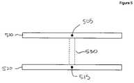
- FIG. 5diagrammatically illustrates exemplary spatial positioning relationships produced by the present invention.
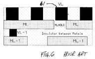
- FIG. 6illustrates a via punch-through problem in conventional integrated circuits.
- the present inventioncan provide a reduction in the intersection of vias in the last layer (“VL”) and holes in the last thin metal layer (“MLHOLE”) without degrading product yield or robustness or increasing copper dishing.
- VLlast layer
- MLHOLElast thin metal layer
- the mutation of some of the dense redundant VLs to MLHOLEs in conjunction with, in some exemplary embodiments, the expansion of some other VLs,can decrease the number of intersections between VLs and MLHOLEs.
- the VL expansion, as well as expansion of the new MLHOLEscan be performed in accordance with a spacing rule between MLHOLE and VL. Although there is a reduction in the total number of VLs, the expanded VLs can still result in an increase in contact area.
- the expansion of the new MLHOLEscan permit a reduction in the percentage of VLs to be mutated.
- An exemplary redundant via arraycan include 30 ⁇ 30 VLs (900 VLs), conventionally sized at 0.4 ⁇ 0.4 ⁇ m 2 each and spaced 0.4 ⁇ m apart.
- VLs900 VLs
- standard MLHOLEs of 0.4 ⁇ 0.4 ⁇ m 2cannot be placed within the array without at least touching the VLs at their corners.
- One way to generate standard-sized MLHOLEs that do not touch any VLswould be to mutate some VLs into MLHOLEs.
- the optimal percentage of VLs to be mutatedcan be based on the copper process. For example, for 130 nm CMOS technology with SiLK (Silicon insulation with Low K), the optimal percentage is about 20%.
- FIG. 1illustrates an exemplary flow diagram for identifying and modifying redundant via arrays in accordance with the present invention.
- regions of redundant via arrayscan be identified in block 110 .
- Redundant via arraysshould have at least 2 ⁇ 2 VLs at close spacing (i.e., the distance between VLs would not allow the insertion of an MLHOLE without the MLHOLE intersecting a VL).
- a marker templatecan be created based on predetermined size and spacing specifications (e.g., VLs of 0.4 ⁇ 0.4 ⁇ m 2 and spaced 0.4 ⁇ m apart, MLHOLEs of 0.4 ⁇ 0.4 ⁇ m 2 and a 0.1 ⁇ m spacing rule).
- the VLs to be mutatedcan be marked in block 120 .
- the marked VLscan then be renamed to create MLHOLEs in block 125 and, in some embodiments, these new MLHOLEs can be expanded. Additional VLs can be expanded as permitted by the spacing rule in block 130 .
- the black squaresrepresent the VLs that were not mutated from the original array
- the cross-hatched rectanglesrepresent expanded VLs
- the white squaresrepresent MLHOLEs.
- the exemplary embodiments of FIGS. 2 and 3are based on a spacing rule of 0.1 ⁇ m between VLs and MLHOLEs. This spacing was based on the assumptions that the VL to MLHOLE misalignment is 0.07 ⁇ m and that the individual shape tolerance is 0.05 ⁇ m.
- FIG. 5illustrates examples of the spatial relationship described by the phrase “relatively overlying.”
- both point 505 and point 515are in a relatively overlying relationship with the via array position formerly occupied by via 530 (shown in broken line), regardless of which of metal layers 510 and 520 is closest to the semiconductor substrate (not shown).
- 75% of the VLs in the original redundant via arrayhave been mutated either to an expanded VL or to an MLHOLE.
- a sparser sample of VLshas been mutated either to an expanded VL or to an MLHOLE to achieve the exemplary embodiment of FIG. 3 and, in FIG.
- FIG. 4tablularizes the exemplary embodiments of FIGS. 2 and 3 .
- the original redundant via arraycontained 900 VLs (a 30 ⁇ 30 array) and the area of the rectangle enclosing the region is 556.96 ⁇ m 2 .
- MLHOLEs over VL-1can also be removed.
- new MLHOLEscan be freely inserted between redundant VLs without mutation. Since mutation introduces changes in shape count and shape size, the layout design data volume may grow by a factor of approximately 2 ⁇ . For other devices, such as a field programmable gate array (“FPGA”), the data volume may decrease because the original MLHOLEs are relatively flat.
- FPGAfield programmable gate array
- the processingincludes the mutation of closely-spaced VLs, the generation of new holes between VLs more widely-spaced, and the removal of MLHOLEs contacting VL-1 or close to a VL.
- Exemplary embodiments of the present inventioncan be included in redundant via generation routines to pre-generate the larger holes. Standard cheesing operations can then follow to complete the hole generation outside regions of dense redundant vias.
- the VL to MLHOLE spacing rule conventionally used in standard cheesing routinescan be modified to match the spacing rule used in the mutation process (e.g., 0.1 ⁇ m).
Landscapes
- Engineering & Computer Science (AREA)
- Computer Hardware Design (AREA)
- Physics & Mathematics (AREA)
- General Physics & Mathematics (AREA)
- Theoretical Computer Science (AREA)
- Evolutionary Computation (AREA)
- General Engineering & Computer Science (AREA)
- Geometry (AREA)
- Condensed Matter Physics & Semiconductors (AREA)
- Microelectronics & Electronic Packaging (AREA)
- Power Engineering (AREA)
- Design And Manufacture Of Integrated Circuits (AREA)
- Internal Circuitry In Semiconductor Integrated Circuit Devices (AREA)
Abstract
Description
Claims (9)
Priority Applications (4)
| Application Number | Priority Date | Filing Date | Title |
|---|---|---|---|
| US10/703,100US7188321B2 (en) | 2003-11-06 | 2003-11-06 | Generation of metal holes by via mutation |
| PCT/EP2004/052833WO2005045932A1 (en) | 2003-11-06 | 2004-11-05 | Generation of metal holes by via mutation |
| US11/653,598US7875544B2 (en) | 2003-11-06 | 2007-01-16 | Method of producing a semiconductor interconnect architecture including generation of metal holes by via mutation |
| US12/966,763US8378493B2 (en) | 2003-11-06 | 2010-12-13 | Generation of metal holes by via mutation |
Applications Claiming Priority (1)
| Application Number | Priority Date | Filing Date | Title |
|---|---|---|---|
| US10/703,100US7188321B2 (en) | 2003-11-06 | 2003-11-06 | Generation of metal holes by via mutation |
Related Child Applications (1)
| Application Number | Title | Priority Date | Filing Date |
|---|---|---|---|
| US11/653,598DivisionUS7875544B2 (en) | 2003-11-06 | 2007-01-16 | Method of producing a semiconductor interconnect architecture including generation of metal holes by via mutation |
Publications (2)
| Publication Number | Publication Date |
|---|---|
| US20050098898A1 US20050098898A1 (en) | 2005-05-12 |
| US7188321B2true US7188321B2 (en) | 2007-03-06 |
Family
ID=34551823
Family Applications (3)
| Application Number | Title | Priority Date | Filing Date |
|---|---|---|---|
| US10/703,100Expired - Fee RelatedUS7188321B2 (en) | 2003-11-06 | 2003-11-06 | Generation of metal holes by via mutation |
| US11/653,598Expired - Fee RelatedUS7875544B2 (en) | 2003-11-06 | 2007-01-16 | Method of producing a semiconductor interconnect architecture including generation of metal holes by via mutation |
| US12/966,763Expired - Fee RelatedUS8378493B2 (en) | 2003-11-06 | 2010-12-13 | Generation of metal holes by via mutation |
Family Applications After (2)
| Application Number | Title | Priority Date | Filing Date |
|---|---|---|---|
| US11/653,598Expired - Fee RelatedUS7875544B2 (en) | 2003-11-06 | 2007-01-16 | Method of producing a semiconductor interconnect architecture including generation of metal holes by via mutation |
| US12/966,763Expired - Fee RelatedUS8378493B2 (en) | 2003-11-06 | 2010-12-13 | Generation of metal holes by via mutation |
Country Status (2)
| Country | Link |
|---|---|
| US (3) | US7188321B2 (en) |
| WO (1) | WO2005045932A1 (en) |
Cited By (1)
| Publication number | Priority date | Publication date | Assignee | Title |
|---|---|---|---|---|
| US20060105564A1 (en)* | 2004-11-17 | 2006-05-18 | Taravade Kunal N | Method and system for reducing inter-layer capacitance in integrated circuits |
Families Citing this family (4)
| Publication number | Priority date | Publication date | Assignee | Title |
|---|---|---|---|---|
| US5910854A (en) | 1993-02-26 | 1999-06-08 | Donnelly Corporation | Electrochromic polymeric solid films, manufacturing electrochromic devices using such solid films, and processes for making such solid films and devices |
| AU2006342115A1 (en) | 2005-12-20 | 2007-10-25 | Board Of Regents Of The University Of Texas System | Nanoporous substrates for analytical methods |
| DE102015121563B4 (en)* | 2015-12-10 | 2023-03-02 | Infineon Technologies Ag | Semiconductor devices and a method of forming a semiconductor device |
| US10304803B2 (en)* | 2016-05-05 | 2019-05-28 | Invensas Corporation | Nanoscale interconnect array for stacked dies |
Citations (7)
| Publication number | Priority date | Publication date | Assignee | Title |
|---|---|---|---|---|
| US5763955A (en) | 1996-07-01 | 1998-06-09 | Vlsi Technology, Inc. | Patterned filled layers for integrated circuit manufacturing |
| US5798937A (en)* | 1995-09-28 | 1998-08-25 | Motorola, Inc. | Method and apparatus for forming redundant vias between conductive layers of an integrated circuit |
| US6100589A (en) | 1996-08-20 | 2000-08-08 | Seiko Epson Corporation | Semiconductor device and a method for making the same that provide arrangement of a connecting region for an external connecting terminal |
| US20010030368A1 (en) | 2000-04-14 | 2001-10-18 | Kazuhiro Tasaka | Semiconductor device and fabrication method |
| WO2003079240A2 (en) | 2002-03-12 | 2003-09-25 | Ubitech, Inc. | System and method for placement of dummy metal fills while preserving device matching and/or limiting capacitance increase |
| US20030229866A1 (en)* | 2002-06-11 | 2003-12-11 | International Business Machines Corporation | Method for improving chip yields in the presence of via flaring |
| US20040063228A1 (en)* | 2002-09-30 | 2004-04-01 | Sun Microsystems, Inc. | Redundant via rule check in a multi-wide object class design layout |
Family Cites Families (7)
| Publication number | Priority date | Publication date | Assignee | Title |
|---|---|---|---|---|
| KR0136684B1 (en)* | 1993-06-01 | 1998-04-29 | Matsushita Electric Industrial Co Ltd | Semiconductor device and manufacture thereof |
| US5446311A (en)* | 1994-09-16 | 1995-08-29 | International Business Machines Corporation | High-Q inductors in silicon technology without expensive metalization |
| US5757077A (en)* | 1995-02-03 | 1998-05-26 | National Semiconductor Corporation | Integrated circuits with borderless vias |
| US6222136B1 (en)* | 1997-11-12 | 2001-04-24 | International Business Machines Corporation | Printed circuit board with continuous connective bumps |
| US6037649A (en)* | 1999-04-01 | 2000-03-14 | Winbond Electronics Corp. | Three-dimension inductor structure in integrated circuit technology |
| US6734090B2 (en)* | 2002-02-20 | 2004-05-11 | International Business Machines Corporation | Method of making an edge seal for a semiconductor device |
| KR100455891B1 (en)* | 2002-12-24 | 2004-11-06 | 삼성전기주식회사 | A printed circuit board with embedded capacitors, and a manufacturing process thereof |
- 2003
- 2003-11-06USUS10/703,100patent/US7188321B2/ennot_activeExpired - Fee Related
- 2004
- 2004-11-05WOPCT/EP2004/052833patent/WO2005045932A1/enactiveApplication Filing
- 2007
- 2007-01-16USUS11/653,598patent/US7875544B2/ennot_activeExpired - Fee Related
- 2010
- 2010-12-13USUS12/966,763patent/US8378493B2/ennot_activeExpired - Fee Related
Patent Citations (7)
| Publication number | Priority date | Publication date | Assignee | Title |
|---|---|---|---|---|
| US5798937A (en)* | 1995-09-28 | 1998-08-25 | Motorola, Inc. | Method and apparatus for forming redundant vias between conductive layers of an integrated circuit |
| US5763955A (en) | 1996-07-01 | 1998-06-09 | Vlsi Technology, Inc. | Patterned filled layers for integrated circuit manufacturing |
| US6100589A (en) | 1996-08-20 | 2000-08-08 | Seiko Epson Corporation | Semiconductor device and a method for making the same that provide arrangement of a connecting region for an external connecting terminal |
| US20010030368A1 (en) | 2000-04-14 | 2001-10-18 | Kazuhiro Tasaka | Semiconductor device and fabrication method |
| WO2003079240A2 (en) | 2002-03-12 | 2003-09-25 | Ubitech, Inc. | System and method for placement of dummy metal fills while preserving device matching and/or limiting capacitance increase |
| US20030229866A1 (en)* | 2002-06-11 | 2003-12-11 | International Business Machines Corporation | Method for improving chip yields in the presence of via flaring |
| US20040063228A1 (en)* | 2002-09-30 | 2004-04-01 | Sun Microsystems, Inc. | Redundant via rule check in a multi-wide object class design layout |
Non-Patent Citations (2)
| Title |
|---|
| Kahng, A.B. et al., "Filling Algorithms and Analyses for Layout Density Control", IEEE Transactions on Computer-Aided Design of Integrated Circuits and Systems, vol. 18, No. 4, Apr. 1999, pp. 445-462. |
| Stine, B.E. et al., "The Physical and Electrical Effects of Metal-Fill Patterning Practices for Oxide Chemical-Mechanical Polishing Processes", IEEE Transactions on Electron Devices, vol. 45, No. 3, Mar. 1998, pp. 665-679. |
Cited By (4)
| Publication number | Priority date | Publication date | Assignee | Title |
|---|---|---|---|---|
| US20060105564A1 (en)* | 2004-11-17 | 2006-05-18 | Taravade Kunal N | Method and system for reducing inter-layer capacitance in integrated circuits |
| US7396760B2 (en)* | 2004-11-17 | 2008-07-08 | Lsi Corporation | Method and system for reducing inter-layer capacitance in integrated circuits |
| US20080235643A1 (en)* | 2004-11-17 | 2008-09-25 | Lsi Logic Corporation | Method and system for reducing inter-layer capacitance in integrated circuits |
| US8015540B2 (en) | 2004-11-17 | 2011-09-06 | Lsi Corporation | Method and system for reducing inter-layer capacitance in integrated circuits |
Also Published As
| Publication number | Publication date |
|---|---|
| US8378493B2 (en) | 2013-02-19 |
| US7875544B2 (en) | 2011-01-25 |
| US20050098898A1 (en) | 2005-05-12 |
| US20110079921A1 (en) | 2011-04-07 |
| WO2005045932A1 (en) | 2005-05-19 |
| US20070118828A1 (en) | 2007-05-24 |
Similar Documents
| Publication | Publication Date | Title |
|---|---|---|
| US10230377B2 (en) | Circuitry and layouts for XOR and XNOR logic | |
| US10777505B2 (en) | Method of fabricating integrated circuit having staggered conductive features | |
| US7424695B2 (en) | Method of manufacturing a semiconductor integrated circuit, a program for a computer automated design system, and a semiconductor integrated circuit | |
| CN100390924C (en) | Semiconductor device and manufacturing method and device thereof | |
| EP0457449A1 (en) | Semiconductor device having via hole and method of producing the same | |
| US8378493B2 (en) | Generation of metal holes by via mutation | |
| US7089522B2 (en) | Device, design and method for a slot in a conductive area | |
| US11694012B2 (en) | Multiplexer | |
| US20070178389A1 (en) | Universal photomask | |
| US20050280159A1 (en) | Computer implemented method for designing a semiconductor device, an automated design system and a semiconductor device | |
| US11392743B2 (en) | Multiplexer | |
| US8680648B2 (en) | Compact metal connect and/or disconnect structures | |
| US7091614B2 (en) | Integrated circuit design for routing an electrical connection | |
| TW201941396A (en) | Staggered self aligned gate contact | |
| JP2006165040A (en) | Semiconductor device and method of designing pattern thereof | |
| US7704848B2 (en) | Method for designing semiconductor device and semiconductor device | |
| US20210143056A1 (en) | Spacer-based conductor cut | |
| US20240006405A1 (en) | Semiconductor structure and manufacturing method thereof | |
| JPH0737987A (en) | Semiconductor integrated circuit wiring method | |
| JP2005109395A (en) | Manufacturing method of mask and manufacturing method of semiconductor device | |
| KR20120068400A (en) | Method for forming semiconductor device |
Legal Events
| Date | Code | Title | Description |
|---|---|---|---|
| AS | Assignment | Owner name:INFINEON TECHNOLOGIES NORTH AMERICA CORP., CALIFOR Free format text:ASSIGNMENT OF ASSIGNORS INTEREST;ASSIGNORS:DEMM, ERNST H.;HIRSCH, ALEXANDER M.;REEL/FRAME:015015/0421;SIGNING DATES FROM 20040115 TO 20040129 Owner name:INTERNATIONAL BUSINESS MACHINES CORPORATION, NEW Y Free format text:ASSIGNMENT OF ASSIGNORS INTEREST;ASSIGNOR:WONG, ROBERT C.;REEL/FRAME:015015/0419 Effective date:20031213 Owner name:UNITED MICROELECTRONICS CO., TAIWAN Free format text:ASSIGNMENT OF ASSIGNORS INTEREST;ASSIGNOR:LEUNG, PAK;REEL/FRAME:015015/0417 Effective date:20040108 | |
| AS | Assignment | Owner name:INFINEON TECHNOLOGIES AG, GERMANY Free format text:ASSIGNMENT OF ASSIGNORS INTEREST;ASSIGNOR:INFINEON TECHNOLOGIES NORTH AMERICA CORP.;REEL/FRAME:015118/0173 Effective date:20040913 | |
| STCF | Information on status: patent grant | Free format text:PATENTED CASE | |
| CC | Certificate of correction | ||
| CC | Certificate of correction | ||
| FPAY | Fee payment | Year of fee payment:4 | |
| FPAY | Fee payment | Year of fee payment:8 | |
| FEPP | Fee payment procedure | Free format text:MAINTENANCE FEE REMINDER MAILED (ORIGINAL EVENT CODE: REM.); ENTITY STATUS OF PATENT OWNER: LARGE ENTITY | |
| LAPS | Lapse for failure to pay maintenance fees | Free format text:PATENT EXPIRED FOR FAILURE TO PAY MAINTENANCE FEES (ORIGINAL EVENT CODE: EXP.); ENTITY STATUS OF PATENT OWNER: LARGE ENTITY | |
| STCH | Information on status: patent discontinuation | Free format text:PATENT EXPIRED DUE TO NONPAYMENT OF MAINTENANCE FEES UNDER 37 CFR 1.362 | |
| FP | Lapsed due to failure to pay maintenance fee | Effective date:20190306 |