US7188219B2 - Buffer control system and method for a memory system having outstanding read and write request buffers - Google Patents
Buffer control system and method for a memory system having outstanding read and write request buffersDownload PDFInfo
- Publication number
- US7188219B2 US7188219B2US10/769,079US76907904AUS7188219B2US 7188219 B2US7188219 B2US 7188219B2US 76907904 AUS76907904 AUS 76907904AUS 7188219 B2US7188219 B2US 7188219B2
- Authority
- US
- United States
- Prior art keywords
- memory
- read
- request
- write
- requests
- Prior art date
- Legal status (The legal status is an assumption and is not a legal conclusion. Google has not performed a legal analysis and makes no representation as to the accuracy of the status listed.)
- Expired - Lifetime, expires
Links
Images


Classifications
- G—PHYSICS
- G06—COMPUTING OR CALCULATING; COUNTING
- G06F—ELECTRIC DIGITAL DATA PROCESSING
- G06F3/00—Input arrangements for transferring data to be processed into a form capable of being handled by the computer; Output arrangements for transferring data from processing unit to output unit, e.g. interface arrangements
- G06F3/06—Digital input from, or digital output to, record carriers, e.g. RAID, emulated record carriers or networked record carriers
- G06F3/0601—Interfaces specially adapted for storage systems
- G06F3/0628—Interfaces specially adapted for storage systems making use of a particular technique
- G06F3/0655—Vertical data movement, i.e. input-output transfer; data movement between one or more hosts and one or more storage devices
- G06F3/0656—Data buffering arrangements
- G—PHYSICS
- G06—COMPUTING OR CALCULATING; COUNTING
- G06F—ELECTRIC DIGITAL DATA PROCESSING
- G06F13/00—Interconnection of, or transfer of information or other signals between, memories, input/output devices or central processing units
- G06F13/14—Handling requests for interconnection or transfer
- G06F13/16—Handling requests for interconnection or transfer for access to memory bus
- G06F13/1605—Handling requests for interconnection or transfer for access to memory bus based on arbitration
- G06F13/1642—Handling requests for interconnection or transfer for access to memory bus based on arbitration with request queuing
- G—PHYSICS
- G06—COMPUTING OR CALCULATING; COUNTING
- G06F—ELECTRIC DIGITAL DATA PROCESSING
- G06F13/00—Interconnection of, or transfer of information or other signals between, memories, input/output devices or central processing units
- G06F13/14—Handling requests for interconnection or transfer
- G06F13/16—Handling requests for interconnection or transfer for access to memory bus
- G06F13/1668—Details of memory controller
- G06F13/1673—Details of memory controller using buffers
- G—PHYSICS
- G06—COMPUTING OR CALCULATING; COUNTING
- G06F—ELECTRIC DIGITAL DATA PROCESSING
- G06F3/00—Input arrangements for transferring data to be processed into a form capable of being handled by the computer; Output arrangements for transferring data from processing unit to output unit, e.g. interface arrangements
- G06F3/06—Digital input from, or digital output to, record carriers, e.g. RAID, emulated record carriers or networked record carriers
- G06F3/0601—Interfaces specially adapted for storage systems
- G06F3/0602—Interfaces specially adapted for storage systems specifically adapted to achieve a particular effect
- G06F3/0604—Improving or facilitating administration, e.g. storage management
- G—PHYSICS
- G06—COMPUTING OR CALCULATING; COUNTING
- G06F—ELECTRIC DIGITAL DATA PROCESSING
- G06F3/00—Input arrangements for transferring data to be processed into a form capable of being handled by the computer; Output arrangements for transferring data from processing unit to output unit, e.g. interface arrangements
- G06F3/06—Digital input from, or digital output to, record carriers, e.g. RAID, emulated record carriers or networked record carriers
- G06F3/0601—Interfaces specially adapted for storage systems
- G06F3/0668—Interfaces specially adapted for storage systems adopting a particular infrastructure
- G06F3/067—Distributed or networked storage systems, e.g. storage area networks [SAN], network attached storage [NAS]
Definitions
- the present inventionis related generally to memory controllers for controlling a memory system, and more particularly, related to memory controllers for managing a memory system having memory request buffers.
- Computer systemsuse memory devices, such as dynamic random access memory (“DRAM”) devices, to store data that are accessed by a processor. These memory devices are normally used as system memory in a computer system.
- the processorcommunicates with the system memory through a processor bus and a memory controller.
- the memory devices of the system memorytypically arranged in memory modules having multiple memory devices, are coupled through a memory bus to the memory controller.
- the processorissues a memory request, which includes a memory command, such as a read command, and an address designating the location from which data or instructions are to be read.
- the memory controlleruses the command and address to generate appropriate command signals as well as row and column addresses, which are applied to the system memory through the memory bus.
- dataare transferred between the system memory and the processor.
- the memory controlleris often part of a system controller, which also includes bus bridge circuitry for coupling the processor bus to an expansion bus, such as a PCI bus.
- bandwidth limitationsare not related to the memory controllers since the memory controllers sequence data to and from the system memory as fast as the memory devices allow.
- One approach that has been taken to increase bandwidthis to increase the speed of the memory data bus coupling the memory controller to the memory devices.
- the same amount of informationcan be moved over the memory data bus in less time.
- a corresponding increase in bandwidthdoes not result.
- One reason for the non-linear relationship between data bus speed and bandwidthis the hardware limitations within the memory devices themselves. That is, the memory controller has to schedule all memory commands to the memory devices such that the hardware limitations are honored.
- the performance of computer systemsis also limited by latency problems that increase the time required to read data from system memory devices. More specifically, when a memory device read command is coupled to a system memory device, such as a synchronous DRAM (“SDRAM”) device, the read data are output from the SDRAM device only after a delay of several clock periods. Therefore, although SDRAM devices can synchronously output burst data at a high data rate, the delay in initially providing the data can significantly slow the operating speed of a computer system using such SDRAM devices. Increasing the memory data bus speed can be used to help alleviate the latency issue. However, as with bandwidth, the increase in memory data bus speeds do not yield a linear reduction of latency, for essentially the same reasons previously discussed.
- SDRAMsynchronous DRAM
- a system controller or memory controlleris coupled over a high speed bi-directional or unidirectional memory controller/hub interface to several memory modules.
- the memory modulesare coupled in a point-to-point or daisy chain architecture such that the memory modules are connected one to another in series.
- the memory controlleris coupled to a first memory module, with the first memory module connected to a second memory module, and the second memory module coupled to a third memory module, and so on in a daisy chain fashion.
- Each memory moduleincludes a memory hub that is coupled to the memory controller/hub interface and a number of memory devices on the module, with the memory hubs efficiently routing memory requests and responses between the controller and the memory devices over the memory controller/hub interface.
- Computer systems employing this architecturecan use a high-speed memory data bus since signal integrity can be maintained on the memory data bus.
- this architecturealso provides for easy expansion of the system memory without concern for degradation in signal quality as more memory modules are added, such as occurs in conventional memory bus architectures.
- managing the use of the various buffers in the memory systemmay require accommodating different buffer management goals. For example, it is desirable to allow for a large number of write requests to be issued to the system memory, while minimizing the number of outstanding read requests. Therefore, there is a need for a system and method for managing buffers of a system memory.
- a memory controllerincludes a memory request queue to receive and store memory requests where the memory request queue issues read requests and write requests to the system memory in response to a flow control signal.
- the memory controllerfurther includes a response queue coupled to receive a memory request response having a status signal identifying read requests and write requests that have been serviced by the system memory.
- a memory request flow control circuitcoupled to the response queue to receive the status signals.
- the memory request flow control circuitincludes separate read and write request monitor circuits to monitor the number of outstanding read and write requests issued to the system memory, respectively.
- the memory request flow control circuitis also coupled to the memory request queue to provide the flow control signal responsive to the number of outstanding read and write requests to control the issuance of read requests and the issuance of write requests to the system memory.
- a method for managing the issuance of read and write requests to a system memoryincludes separately monitoring the number of outstanding read requests and write requests issued to the system memory, and separately controlling further issuance of read and write requests to the system memory based on the number of outstanding read and write requests, respectively.
- the issuance of read and write requestsare managed by independently halting and resuming the issuance of read and write requests to the system memory to maintain the number of outstanding read requests between first and second read thresholds and to maintain the number of outstanding write requests between first and second write thresholds, respectively.
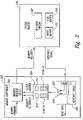
- FIG. 1is a partial block diagram of a computer system in which embodiments of the present invention can be implemented.
- FIG. 2is a partial block diagram of a memory controller according to an embodiment of the present invention.
- FIG. 3is a partial block diagram of a memory controller according to an alternative embodiment of the present invention.
- FIG. 4is a partial block diagram of a computer system having a memory hub based system memory in which embodiments of the present invention can be implemented.
- FIG. 1illustrates a computer system 100 according to an embodiment of the present invention.
- the computer system 100includes a processor 102 for performing various computing functions, such as executing specific software to perform specific calculations or tasks.
- the processor 102includes a processor bus 104 that normally includes an address bus, a control bus, and a data bus.
- the processor bus 104is typically coupled to a cache memory 106 , which, is typically static random access memory (“SRAM”) device.
- SRAMstatic random access memory
- the processor bus 104is further coupled to a system controller 108 , which is also sometimes referred to as a bus bridge.
- the system controller 108serves as a communications path to the processor 102 for a variety of other components. As shown in FIG.
- the system controller 108includes a graphics port that is typically coupled to a graphics controller 110 , which is, in turn, coupled to a video terminal 112 .
- the system controller 108is also coupled to one or more input devices 114 , such as a keyboard or a mouse, to allow an operator to interface with the computer system 100 .
- the computer system 100also includes one or more output devices 116 , such as a printer, coupled to the processor 102 through the system controller 108 .
- One or more data storage devices 118are also typically coupled to the processor 102 through the system controller 108 to allow the processor 102 to store data or retrieve data from internal or external storage media (not shown). Examples of typical storage devices 118 include hard and floppy disks, tape cassettes, and compact disk read-only memories (CD-ROMs).
- the system controller 108includes a memory controller 124 that is coupled to the processor 102 .
- the memory controller 124is also coupled to a system memory 120 through a system memory bus 122 on which data, address and/or control signals are coupled away from or toward the memory controller 124 .
- the system memory 120includes a plurality of memory devices 130 coupled to the system memory bus 122 , and further includes write buffers 132 and read data buffers 134 also coupled to the system memory bus 122 .
- the system memory 120is used to store information, typically data or instructions, for use by the rest of the computer system 100 , such as, the processor 102 , the graphics controller 110 , input or output devices 114 , 116 , and the like. However, the system memory 120 shown in FIG.
- 1is an “intelligent” memory system that can monitor the types of memory requests issued by the memory controller 124 , for example, read requests or write requests, as well as alter the order in which the memory requests are executed from the order in which the memory requests are issued by the memory controller 124 . Additionally, the system memory 120 can also modify the flow of read data provided to the memory controller 124 from the order in which the read data is requested by the memory controller 124 . The reordering of the memory requests as well as the return read data is made to improve utilization of the system memory bus 122 . Handling of the memory requests and read data is facilitated by the use of the write buffer 132 and the read data buffer 134 included in the system memory 120 . For example, the write buffer 132 and the read data buffer 134 are used to temporarily store write requests and read data, respectively, in the memory system 120 until a sufficient number of write requests are ready for servicing or until the appropriate time for transferring read data to the memory controller 124 .
- a memory request response circuit 140for monitoring the servicing of memory requests issued by the memory request queue 204 .
- an appropriate response signalis generated by the memory request response circuit 140 .
- the memory request response circuit 140when a read request issued to the system memory 120 is serviced, and read data is ready to be provided to the memory controller 124 , the memory request response circuit 140 generates a read response signal that includes the read data signals as well as a read status signal that identifies the read request corresponding to the read data. With respect to a write request that has been serviced by the system memory 120 , the memory request response circuit 140 generates a write response signal that includes a write status signal indicating that the particular write request has been serviced by the system memory 120 .
- the response signals generated by the memory request response circuitare used by the memory controller 124 to monitor the number of outstanding memory requests issued to the system memory 120 .
- the system memory 120includes a memory request response circuit 140 to provide response signals to the memory controller 124 .
- alternative approaches known in the artcan be used to report the servicing of read and write requests to the memory controller 124 . In the interest of brevity, such alternative approaches will not be discussed herein.
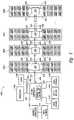
- FIG. 2illustrates a portion memory controller 202 according to an embodiment of the present invention.
- the memory controller 202can be substituted for the memory controller 124 shown in FIG. 1 .
- the memory controller 202includes a memory request queue 204 that receives from the processor 104 ( FIG. 1 ) via the system controller 108 high level memory request signals, including command signals, address signals and, in the case of a memory write, write data signals.
- the memory request queue 204also receives Request ID signals from a flow control unit 208 that uniquely identify each memory request. These Request IDs are combined with corresponding high level memory requests and stored in the memory request queue 204 , preferably in the order they are received.
- the memory request signals stored in the request queue 204include both read request signals and write request signals.
- the high level memory request signals and the Request ID signalswill collectively be referred to as memory request signals.
- the memory controller 202also includes a memory response queue 220 that receives read response signals and write response signals from the system memory 120 .
- the read response signalsinclude read data signals as well as read status signals that identify the read request corresponding to the read data.
- the write response signalsinclude write status signals that identify a write request that has been serviced by one of the memory modules.
- the response signalsare generated by a memory request response circuit 140 ( FIG. 1 ) included in the system memory 120 to allow the memory controller 202 to monitor the number of outstanding read and write requests that have been issued to the system memory 120 .
- the memory response queue 220couples read status signals 222 and write status signals 224 to the flow control unit 208 so the flow control unit 208 can determine which read requests and which write requests have been serviced by the system memory 120 .
- the flow control unit 208makes this determination by comparing the status signals 222 , 224 to the Request IDs generated and coupled to the memory request queue 204 .
- the flow control unit 208includes read and write buffer control circuits 210 , 212 , which are used for independently monitoring the number of outstanding read and write requests issued to the system memory 120 , respectively.
- the flow control unit 208outputs flow control signals based on the number of outstanding read and write requests to the memory request queue 204 to control whether and when additional read or write requests should be issued to the system memory 120 .
- the read buffer control circuit 210 and the write buffer control circuit 212include up/down counter circuits 214 , 216 for monitoring outstanding read and write requests issued to the system memory 120 .
- the counter circuit 214is incremented by the flow control unit 208 in response to the issuance of a read request to the system memory 120 , and is decremented in response to the receipt of a read status signal 222 for the corresponding read request. In this manner, the value of the counter circuit 214 is indicative of the number of outstanding read requests issued to the system memory 120 .
- the counter circuit 216is used to monitor the number of outstanding write requests in the same manner as previously described with respect to the counter circuit 214 for monitoring the outstanding read requests.
- the flow control unit 208monitors the number of outstanding read and write requests through the use of the read and write buffer control circuits 210 , 212 , and the up/down counter circuits 214 and 216 . In response to the number of outstanding memory requests, the flow control unit 208 outputs flow control signals to halt or resume further issuance of read or write requests to the system memory 120 . In this manner, the flow control unit 208 can prevent overrunning the posted write buffers 132 and the read data buffers 134 of the memory system 120 . Additionally, allowing for the number of outstanding read requests before halting further issuance of read requests to be different than the number of outstanding write requests before halting further issuance of write requests provides the flexibility to accommodate differences in buffer management between read and write requests. For example, it is generally the case that a large number of outstanding write requests issued to the system memory 120 is acceptable, and in some cases, preferable, whereas the number of outstanding read requests issued to the system memory 120 is preferably minimized.
- the read buffer control circuit 210stores a programmable read request limit that defines the number of outstanding read requests that may be issued to the system memory 120 before the flow control unit 208 outputs a control signal to the memory request queue 204 halting further issuance of read requests.
- the write buffer control circuit 212stores a programmable write request limit that defines the number of outstanding write requests that may be issued to the system memory 120 before the flow control unit 208 outputs a control signal to halt further issuance of write requests.
- the read and write request limits, and the read and write resume limithave been previously described as being programmable, it will be appreciated that the read and write request limits and the read and write resume limits can be a fixed value as well.
- programmable read and write buffer limits programmed into the read and write buffer control circuits 210 , 212allow for the buffer control to be tailored for the particular type of memory request, that is, either read requests or write requests, as well as to allow values to be selected that are indicative of the allowable read and write buffer depths of the system memory 120 . It will be appreciated that in alternative embodiments, rather than have non-zero read and write resume limits, issuance of read or write requests can resume when the number of outstanding read or write requests decrease to zero.
- FIG. 2illustrates a portion memory controller 202 according to an embodiment of the present invention.
- the memory controller 202can be substituted for the memory controller 124 shown in FIG. 1 .
- the memory controller 202includes a memory request queue 204 that receives from the processor 104 ( FIG. 1 ) via the system controller 108 high level memory request signals, including command signals, address signals and, in the case of a memory write, write data signals.
- the memory request queue 204also receives Request ID signals from a flow control unit 208 that uniquely identify each memory request. These Request IDs are combined with corresponding high level memory requests and stored in the memory request queue 204 , preferably in the order they are received.
- the memory request signals stored in the request queue 204include both read request signals and write request signals.
- the high level memory request signals and the Request ID signalswill collectively be referred to as memory request signals.
- the flow control circuit 208 of the memory controller 202included read and write buffer control circuits 210 , 212 to monitor the number of outstanding read and write requests issued to the system memory 120 .
- the memory controller 302includes a plurality of read buffer control circuits 310 a–d and a plurality of write buffer control circuits 312 a–d .
- Each of the read buffer control circuits 310 a–dhas a programmable read request limit and a programmable read resume limit
- each of the write buffer control circuitshas a programmable write request limit and a programmable write resume limit.
- Each of the read buffer control circuits 310 a–dcan be used to individually monitor a corresponding read data buffer in the system memory 120 .
- each of the write buffer control circuits 312 a–dcan be used to individually monitor a corresponding write buffer in the system memory 120 .
- the memory controller 202 described with respect to FIG. 2monitored the total number of outstanding read requests issued to the system memory 120 using the read buffer control circuit 210 and further monitored the total number of outstanding write requests issued to the system memory 120 using the write buffer control circuit 212 .
- the individual read and write request limits, and the individual read and write resume limits for the memory controller 302can be fixed rather than programmable, or alternatively, some combination of fixed and programmable values.
- the read and write buffer control circuits 310 a–d , 312 a–dcan be implemented using counter circuits, as previously described with respect to the memory controller 202 .
- those ordinarily skilled in the artwill obtain sufficient understanding from the description provided herein to practice the invention using other well known or later developed designs and circuits. Consequently, the scope of the present invention should not be limited to any of the particular embodiments described herein, or to the use of any particular circuits described with respect to those embodiments.
- FIG. 4illustrates a computer system 400 having a memory hub architecture in which embodiments of the present invention can be utilized.
- the computer system 400includes a processor 404 for performing various computing functions, such as executing specific software to perform specific calculations or tasks.
- the processor 404includes a processor bus 406 that normally includes an address bus, a control bus, and a data bus.
- the processor bus 406is typically coupled to cache memory 408 , which, is typically static random access memory (“SRAM”).
- SRAMstatic random access memory
- the processor bus 406is coupled to a system controller 410 , which is also sometimes referred to as a bus bridge.
- the system controller 410also serves as a communications path to the processor 404 for a variety of other components. More specifically, the system controller 410 includes a graphics port that is typically coupled to a graphics controller 412 , which is, in turn, coupled to a video terminal 414 . The system controller 410 is also coupled to one or more input devices 418 , such as a keyboard or a mouse, to allow an operator to interface with the computer system 400 . Typically, the computer system 400 also includes one or more output devices 420 , such as a printer, coupled to the processor 404 through the system controller 410 . One or more data storage devices 424 are also typically coupled to the processor 404 through the system controller 410 to allow the processor 404 to store data or retrieve data from internal or external storage media (not shown). Examples of typical storage devices 424 include hard and floppy disks, tape cassettes, and compact disk read-only memories (CD-ROMs).
- CD-ROMscompact disk read-only memories
- the system controller 410contains a memory hub controller 428 coupled to several memory modules 430 a–n through a bus system 454 , 456 .
- Each of the memory modules 430 a–nincludes a memory hub 440 coupled to several memory devices 448 through command, address and data buses, collectively shown as bus 450 .
- the memory hub 440efficiently routes memory requests and responses between the controller 428 and the memory devices 448 .
- Each of the memory hubs 440includes write buffers and read data buffers, as previously described. Computer systems employing this architecture allow for the processor 404 to access one memory module 430 a–n while another memory module 430 a–n is responding to a prior memory request.
- the processor 404can output write data to one of the memory modules 430 a–n in the system while another memory module 430 a–n in the system is preparing to provide read data to the processor 404 .
- a memory hub architecturecan also provide greatly increased memory capacity in computer systems.
- the memory hub controller 428includes circuits according to an embodiment of the present invention. That is, outstanding read and write requests are independently monitored, and in response to the number of outstanding read and write requests, the further issuance of read or write requests can be halted until the number of outstanding read or write requests decreases below a resume limit, at which time, issuance of the read or write requests to the memory may resume. In this manner, separate monitoring and control over the issuance of read requests and monitoring and control over the issuance of write requests to the system memory allows for independent buffer control.
Landscapes
- Engineering & Computer Science (AREA)
- Theoretical Computer Science (AREA)
- Physics & Mathematics (AREA)
- General Engineering & Computer Science (AREA)
- General Physics & Mathematics (AREA)
- Human Computer Interaction (AREA)
- Debugging And Monitoring (AREA)
- Memory System Of A Hierarchy Structure (AREA)
- Information Transfer Systems (AREA)
- Techniques For Improving Reliability Of Storages (AREA)
Abstract
Description
Claims (81)
Priority Applications (4)
| Application Number | Priority Date | Filing Date | Title |
|---|---|---|---|
| US10/769,079US7188219B2 (en) | 2004-01-30 | 2004-01-30 | Buffer control system and method for a memory system having outstanding read and write request buffers |
| TW094102706ATWI382308B (en) | 2004-01-30 | 2005-01-28 | Buffer control system and method for memory system with memory request buffer |
| US11/650,218US8504782B2 (en) | 2004-01-30 | 2007-01-04 | Buffer control system and method for a memory system having outstanding read and write request buffers |
| US13/960,243US8788765B2 (en) | 2004-01-30 | 2013-08-06 | Buffer control system and method for a memory system having outstanding read and write request buffers |
Applications Claiming Priority (1)
| Application Number | Priority Date | Filing Date | Title |
|---|---|---|---|
| US10/769,079US7188219B2 (en) | 2004-01-30 | 2004-01-30 | Buffer control system and method for a memory system having outstanding read and write request buffers |
Related Child Applications (1)
| Application Number | Title | Priority Date | Filing Date |
|---|---|---|---|
| US11/650,218ContinuationUS8504782B2 (en) | 2004-01-30 | 2007-01-04 | Buffer control system and method for a memory system having outstanding read and write request buffers |
Publications (2)
| Publication Number | Publication Date |
|---|---|
| US20050172084A1 US20050172084A1 (en) | 2005-08-04 |
| US7188219B2true US7188219B2 (en) | 2007-03-06 |
Family
ID=34808037
Family Applications (3)
| Application Number | Title | Priority Date | Filing Date |
|---|---|---|---|
| US10/769,079Expired - LifetimeUS7188219B2 (en) | 2004-01-30 | 2004-01-30 | Buffer control system and method for a memory system having outstanding read and write request buffers |
| US11/650,218Expired - LifetimeUS8504782B2 (en) | 2004-01-30 | 2007-01-04 | Buffer control system and method for a memory system having outstanding read and write request buffers |
| US13/960,243Expired - LifetimeUS8788765B2 (en) | 2004-01-30 | 2013-08-06 | Buffer control system and method for a memory system having outstanding read and write request buffers |
Family Applications After (2)
| Application Number | Title | Priority Date | Filing Date |
|---|---|---|---|
| US11/650,218Expired - LifetimeUS8504782B2 (en) | 2004-01-30 | 2007-01-04 | Buffer control system and method for a memory system having outstanding read and write request buffers |
| US13/960,243Expired - LifetimeUS8788765B2 (en) | 2004-01-30 | 2013-08-06 | Buffer control system and method for a memory system having outstanding read and write request buffers |
Country Status (2)
| Country | Link |
|---|---|
| US (3) | US7188219B2 (en) |
| TW (1) | TWI382308B (en) |
Cited By (48)
| Publication number | Priority date | Publication date | Assignee | Title |
|---|---|---|---|---|
| US20050223161A1 (en)* | 2002-08-05 | 2005-10-06 | Jeddeloh Joseph M | Memory hub and access method having internal row caching |
| US20060120376A1 (en)* | 2004-12-06 | 2006-06-08 | Nvidia Corporation | Method and apparatus for providing peer-to-peer data transfer within a computing environment |
| US20060224807A1 (en)* | 2005-03-30 | 2006-10-05 | Canon Kabushiki Kaisha | Recording apparatus and recording control method for executing recording according to setting of print parameters |
| US20070033353A1 (en)* | 2004-05-14 | 2007-02-08 | Jeddeloh Joseph M | Memory hub and method for memory sequencing |
| US20070038907A1 (en)* | 2005-08-01 | 2007-02-15 | Micron Technology, Inc. | Testing system and method for memory modules having a memory hub architecture |
| US20070041255A1 (en)* | 2005-08-19 | 2007-02-22 | Micron Technology, Inc. | System and method for injecting phase jitter into integrated circuit test signals |
| US20070055817A1 (en)* | 2002-06-07 | 2007-03-08 | Jeddeloh Joseph M | Memory hub with internal cache and/or memory access prediction |
| US20070186069A1 (en)* | 2004-08-10 | 2007-08-09 | Moir Mark S | Coordinating Synchronization Mechanisms using Transactional Memory |
| US20070200579A1 (en)* | 2005-08-01 | 2007-08-30 | Micron Technology, Inc. | Integrated circuit load board and method having on-board test circuit |
| US20070271435A1 (en)* | 2002-08-29 | 2007-11-22 | Jeddeloh Joseph M | Method and system for controlling memory accesses to memory modules having a memory hub architecture |
| US7355387B2 (en) | 2005-12-08 | 2008-04-08 | Micron Technology, Inc. | System and method for testing integrated circuit timing margins |
| US20080222323A1 (en)* | 2006-06-14 | 2008-09-11 | Genesys Logic, Inc. | Multimedia adapting apparatus |
| US20080301324A1 (en)* | 2006-02-27 | 2008-12-04 | Fujitsu Limited | Processor device and instruction processing method |
| US7469309B1 (en)* | 2005-12-12 | 2008-12-23 | Nvidia Corporation | Peer-to-peer data transfer method and apparatus with request limits |
| US20090006705A1 (en)* | 2007-06-27 | 2009-01-01 | Gerald Keith Bartley | Hub for Supporting High Capacity Memory Subsystem |
| US20090006752A1 (en)* | 2007-06-27 | 2009-01-01 | Gerald Keith Bartley | High Capacity Memory Subsystem Architecture Employing Hierarchical Tree Configuration of Memory Modules |
| US20090006781A1 (en)* | 2007-06-27 | 2009-01-01 | International Business Machines Corporation | Structure for Memory Chip for High Capacity Memory Subsystem Supporting Multiple Speed Bus |
| US20090006790A1 (en)* | 2007-06-27 | 2009-01-01 | Gerald Keith Bartley | High Capacity Memory Subsystem Architecture Storing Interleaved Data for Reduced Bus Speed |
| US20090006772A1 (en)* | 2007-06-27 | 2009-01-01 | Gerald Keith Bartley | Memory Chip for High Capacity Memory Subsystem Supporting Replication of Command Data |
| US20090006760A1 (en)* | 2007-06-27 | 2009-01-01 | International Business Machines Corporation | Structure for Dual-Mode Memory Chip for High Capacity Memory Subsystem |
| US20090006715A1 (en)* | 2007-06-27 | 2009-01-01 | Gerald Keith Bartley | Memory Chip for High Capacity Memory Subsystem Supporting Multiple Speed Bus |
| US20090006689A1 (en)* | 2007-06-29 | 2009-01-01 | Seagate Technology Llc | Command queue management of back watered requests |
| US20090006798A1 (en)* | 2007-06-27 | 2009-01-01 | International Business Machines Corporation | Structure for Memory Chip for High Capacity Memory Subsystem Supporting Replication of Command Data |
| US20090006706A1 (en)* | 2007-06-27 | 2009-01-01 | International Business Machines Corporation | Structure for Hub for Supporting High Capacity Memory Subsystem |
| US20090006775A1 (en)* | 2007-06-27 | 2009-01-01 | Gerald Keith Bartley | Dual-Mode Memory Chip for High Capacity Memory Subsystem |
| US20090225609A1 (en)* | 2005-05-30 | 2009-09-10 | Seiko Epson Corporation | Semiconductor memory device |
| US20100067042A1 (en)* | 2008-09-16 | 2010-03-18 | Junichi Ikeda | Image forming apparatus and data transferring method |
| US20100131722A1 (en)* | 2008-11-25 | 2010-05-27 | Mediatek Inc. | Apparatus and method for buffer management for a memory operating |
| US8127081B2 (en) | 2003-06-20 | 2012-02-28 | Round Rock Research, Llc | Memory hub and access method having internal prefetch buffers |
| US8195858B1 (en)* | 2009-07-28 | 2012-06-05 | Nvidia Corporation | Managing conflicts on shared L2 bus |
| US8239607B2 (en) | 2004-06-04 | 2012-08-07 | Micron Technology, Inc. | System and method for an asynchronous data buffer having buffer write and read pointers |
| US8321618B1 (en) | 2009-07-28 | 2012-11-27 | Nvidia Corporation | Managing conflicts on shared L2 bus |
| WO2013005121A1 (en)* | 2011-07-06 | 2013-01-10 | International Business Machines Corporation | Dynamic data-protection policies associated with a request-reply message queuing environment |
| US8392686B2 (en) | 2003-12-29 | 2013-03-05 | Micron Technology, Inc. | System and method for read synchronization of memory modules |
| US20130151741A1 (en)* | 2011-12-13 | 2013-06-13 | Micron Technology, Inc. | Memory apparatuses, computer systems and methods for ordering memory responses |
| US20130151757A1 (en)* | 2011-12-08 | 2013-06-13 | Pyeon Hong Beom | Independent write and read control in serially-connected devices |
| US8589643B2 (en) | 2003-10-20 | 2013-11-19 | Round Rock Research, Llc | Arbitration system and method for memory responses in a hub-based memory system |
| US8788765B2 (en) | 2004-01-30 | 2014-07-22 | Micron Technology, Inc. | Buffer control system and method for a memory system having outstanding read and write request buffers |
| US9477413B2 (en)* | 2010-09-21 | 2016-10-25 | Western Digital Technologies, Inc. | System and method for managing access requests to a memory storage subsystem |
| US20170060427A1 (en)* | 2015-09-01 | 2017-03-02 | Silicon Motion, Inc. | Methods for scheduling read and write commands and apparatuses using the same |
| US9740188B2 (en) | 2007-05-21 | 2017-08-22 | Honeywell International Inc. | Systems and methods for scheduling the operation of building resources |
| US20180239686A1 (en)* | 2017-02-20 | 2018-08-23 | Tsinghua University | Input and output recording device and method, cpu and data read and write operation method thereof |
| US10572671B2 (en) | 2017-02-20 | 2020-02-25 | Tsinghua University | Checking method, checking system and checking device for processor security |
| US10642981B2 (en) | 2017-02-20 | 2020-05-05 | Wuxi Research Institute Of Applied Technologies Tsinghua University | Checking method, checking device and checking system for processor |
| US10684896B2 (en) | 2017-02-20 | 2020-06-16 | Tsinghua University | Method for processing asynchronous event by checking device and checking device |
| US10853268B2 (en)* | 2016-06-15 | 2020-12-01 | Hitachi, Ltd. | Parity generating information processing system |
| US10977200B2 (en)* | 2019-06-27 | 2021-04-13 | EMC IP Holding Company LLC | Method, apparatus and computer program product for processing I/O request |
| US11349738B2 (en)* | 2016-02-11 | 2022-05-31 | Samsung Electronics Co., Ltd. | Semiconductor device and operating method thereof |
Families Citing this family (46)
| Publication number | Priority date | Publication date | Assignee | Title |
|---|---|---|---|---|
| US6791555B1 (en) | 2000-06-23 | 2004-09-14 | Micron Technology, Inc. | Apparatus and method for distributed memory control in a graphics processing system |
| US7120727B2 (en) | 2003-06-19 | 2006-10-10 | Micron Technology, Inc. | Reconfigurable memory module and method |
| US7107415B2 (en) | 2003-06-20 | 2006-09-12 | Micron Technology, Inc. | Posted write buffers and methods of posting write requests in memory modules |
| US7133991B2 (en)* | 2003-08-20 | 2006-11-07 | Micron Technology, Inc. | Method and system for capturing and bypassing memory transactions in a hub-based memory system |
| US7213082B2 (en) | 2004-03-29 | 2007-05-01 | Micron Technology, Inc. | Memory hub and method for providing memory sequencing hints |
| US8135741B2 (en)* | 2005-09-20 | 2012-03-13 | Microsoft Corporation | Modifying service provider context information to facilitate locating interceptor context information |
| US7444479B2 (en)* | 2005-12-28 | 2008-10-28 | Alexander James W | Fully buffered DIMM read data substitution for write acknowledgement |
| JP4142068B2 (en)* | 2006-06-16 | 2008-08-27 | 株式会社ソニー・コンピュータエンタテインメント | Information processing apparatus and access control method |
| US20080049617A1 (en)* | 2006-08-23 | 2008-02-28 | International Business Machines Corporation | System for fine grained flow-control concurrency to prevent excessive packet loss |
| JP5057792B2 (en)* | 2007-01-29 | 2012-10-24 | 株式会社日立製作所 | Storage system with a function to alleviate performance bottlenecks |
| US20080282050A1 (en)* | 2007-05-07 | 2008-11-13 | On Demand Microelectronics | Methods and arrangements for controlling memory operations |
| US8504784B2 (en)* | 2007-06-27 | 2013-08-06 | Sandisk Technologies Inc. | Scheduling methods of phased garbage collection and housekeeping operations in a flash memory system |
| TWI369633B (en)* | 2007-06-27 | 2012-08-01 | Sandisk Corp | Phased garbage collection and house keeping operations in a flash memory system |
| US8601181B2 (en)* | 2007-11-26 | 2013-12-03 | Spansion Llc | System and method for read data buffering wherein an arbitration policy determines whether internal or external buffers are given preference |
| CN101222444B (en)* | 2008-02-04 | 2011-11-09 | 华为技术有限公司 | Caching data processing method, device and system |
| JP5454224B2 (en)* | 2010-02-25 | 2014-03-26 | ソニー株式会社 | Storage device and storage system |
| US9015415B2 (en)* | 2010-09-24 | 2015-04-21 | Intel Corporation | Multi-processor computing system having fast processor response to cache agent request capacity limit warning |
| US20120095607A1 (en)* | 2011-12-22 | 2012-04-19 | Wells Ryan D | Method, Apparatus, and System for Energy Efficiency and Energy Conservation Through Dynamic Management of Memory and Input/Output Subsystems |
| US9236064B2 (en)* | 2012-02-15 | 2016-01-12 | Microsoft Technology Licensing, Llc | Sample rate converter with automatic anti-aliasing filter |
| US8982624B2 (en) | 2012-10-02 | 2015-03-17 | Fusion-Io, Llc | Adjustable read time for memory |
| JP6146128B2 (en)* | 2013-05-20 | 2017-06-14 | ヤマハ株式会社 | Data processing device |
| KR102034626B1 (en)* | 2013-06-26 | 2019-10-21 | 삼성전자 주식회사 | Method and apparatus for controlling memory operation |
| JP6221467B2 (en)* | 2013-07-29 | 2017-11-01 | 株式会社リコー | Image processing apparatus and control method |
| JP6950149B2 (en)* | 2015-09-08 | 2021-10-13 | ソニーグループ株式会社 | Memory controller, memory system, and memory controller control method |
| US10178041B2 (en)* | 2015-09-23 | 2019-01-08 | Intel Corporation | Technologies for aggregation-based message synchronization |
| US10148483B1 (en)* | 2015-09-30 | 2018-12-04 | EMC IP Holding Company LLC | Dynamic front end connectivity optimizations |
| US10719236B2 (en)* | 2015-11-20 | 2020-07-21 | Arm Ltd. | Memory controller with non-volatile buffer for persistent memory operations |
| KR102717098B1 (en)* | 2016-11-01 | 2024-10-15 | 삼성전자주식회사 | Memory device with stepwise low power states |
| CN108667740B (en)* | 2017-03-29 | 2022-02-15 | 腾讯科技(深圳)有限公司 | Flow control method, device and system |
| US10229059B2 (en) | 2017-03-31 | 2019-03-12 | Intel Corporation | Dynamic fill policy for a shared cache |
| CN107341130B (en) | 2017-06-29 | 2020-11-17 | 上海兆芯集成电路有限公司 | Chip set with near-end data processing engine |
| US10754578B2 (en) | 2018-05-09 | 2020-08-25 | Micron Technology, Inc. | Memory buffer management and bypass |
| US10714159B2 (en)* | 2018-05-09 | 2020-07-14 | Micron Technology, Inc. | Indication in memory system or sub-system of latency associated with performing an access command |
| US11010092B2 (en) | 2018-05-09 | 2021-05-18 | Micron Technology, Inc. | Prefetch signaling in memory system or sub-system |
| US10942854B2 (en) | 2018-05-09 | 2021-03-09 | Micron Technology, Inc. | Prefetch management for memory |
| US10678478B2 (en)* | 2018-08-24 | 2020-06-09 | Apple Inc. | Ordering memory requests based on access efficiency |
| CN109407970B (en)* | 2018-09-12 | 2022-02-11 | 新华三技术有限公司成都分公司 | Read-write request processing method and device and electronic equipment |
| US10969978B2 (en) | 2018-09-25 | 2021-04-06 | Micron Technology, Inc. | Configurable buffer manager arbitration request throttling mechanism |
| KR102725221B1 (en) | 2018-11-16 | 2024-11-01 | 삼성전자주식회사 | Storage device throttling amount of communicated data depending on suspension frequency of operation |
| CN110209597B (en)* | 2019-05-24 | 2021-10-15 | 北京百度网讯科技有限公司 | Method, apparatus, device and storage medium for processing access request |
| US11593025B2 (en)* | 2020-01-15 | 2023-02-28 | Arm Limited | Write operation status |
| US11086853B1 (en)* | 2020-10-12 | 2021-08-10 | iodyne, LLC | Method and system for streaming data from portable storage devices |
| US20230065395A1 (en)* | 2021-08-30 | 2023-03-02 | Micron Technology, Inc. | Command retrieval and issuance policy |
| CN114218145B (en)* | 2021-12-17 | 2025-02-11 | 山东云海国创云计算装备产业创新中心有限公司 | A CHI protocol anti-blocking interconnection method, system, device and storage medium |
| US11836096B2 (en)* | 2021-12-22 | 2023-12-05 | Micron Technology, Inc. | Memory-flow control register |
| WO2024123886A1 (en)* | 2022-12-08 | 2024-06-13 | Micron Technology, Inc. | Memory device active command tracking |
Citations (221)
| Publication number | Priority date | Publication date | Assignee | Title |
|---|---|---|---|---|
| US4045781A (en) | 1976-02-13 | 1977-08-30 | Digital Equipment Corporation | Memory module with selectable byte addressing for digital data processing system |
| US4240143A (en) | 1978-12-22 | 1980-12-16 | Burroughs Corporation | Hierarchical multi-processor network for memory sharing |
| US4245306A (en) | 1978-12-21 | 1981-01-13 | Burroughs Corporation | Selection of addressed processor in a multi-processor network |
| US4253144A (en) | 1978-12-21 | 1981-02-24 | Burroughs Corporation | Multi-processor communication network |
| US4253146A (en) | 1978-12-21 | 1981-02-24 | Burroughs Corporation | Module for coupling computer-processors |
| US4608702A (en) | 1984-12-21 | 1986-08-26 | Advanced Micro Devices, Inc. | Method for digital clock recovery from Manchester-encoded signals |
| US4707823A (en) | 1986-07-21 | 1987-11-17 | Chrysler Motors Corporation | Fiber optic multiplexed data acquisition system |
| US4724520A (en) | 1985-07-01 | 1988-02-09 | United Technologies Corporation | Modular multiport data hub |
| US4891808A (en) | 1987-12-24 | 1990-01-02 | Coherent Communication Systems Corp. | Self-synchronizing multiplexer |
| US4930128A (en) | 1987-06-26 | 1990-05-29 | Hitachi, Ltd. | Method for restart of online computer system and apparatus for carrying out the same |
| US4953930A (en) | 1989-03-15 | 1990-09-04 | Ramtech, Inc. | CPU socket supporting socket-to-socket optical communications |
| US5241506A (en) | 1989-11-15 | 1993-08-31 | Kabushiki Kaisha Toshiba | Semiconductor memory circuit apparatus |
| US5243703A (en) | 1990-04-18 | 1993-09-07 | Rambus, Inc. | Apparatus for synchronously generating clock signals in a data processing system |
| WO1993019422A1 (en) | 1992-03-25 | 1993-09-30 | Encore Computer U.S., Inc. | Fiber optic memory coupling system |
| US5251303A (en) | 1989-01-13 | 1993-10-05 | International Business Machines Corporation | System for DMA block data transfer based on linked control blocks |
| US5269022A (en) | 1990-03-28 | 1993-12-07 | Kabushiki Kaisha Toshiba | Method and apparatus for booting a computer system by restoring the main memory from a backup memory |
| US5317752A (en) | 1989-12-22 | 1994-05-31 | Tandem Computers Incorporated | Fault-tolerant computer system with auto-restart after power-fall |
| US5319755A (en) | 1990-04-18 | 1994-06-07 | Rambus, Inc. | Integrated circuit I/O using high performance bus interface |
| US5327553A (en) | 1989-12-22 | 1994-07-05 | Tandem Computers Incorporated | Fault-tolerant computer system with /CONFIG filesystem |
| US5355391A (en) | 1992-03-06 | 1994-10-11 | Rambus, Inc. | High speed bus system |
| US5432907A (en) | 1992-05-12 | 1995-07-11 | Network Resources Corporation | Network hub with integrated bridge |
| US5432823A (en) | 1992-03-06 | 1995-07-11 | Rambus, Inc. | Method and circuitry for minimizing clock-data skew in a bus system |
| US5442770A (en) | 1989-01-24 | 1995-08-15 | Nec Electronics, Inc. | Triple port cache memory |
| US5461627A (en) | 1991-12-24 | 1995-10-24 | Rypinski; Chandos A. | Access protocol for a common channel wireless network |
| US5465229A (en) | 1992-05-19 | 1995-11-07 | Sun Microsystems, Inc. | Single in-line memory module |
| US5479370A (en) | 1992-02-20 | 1995-12-26 | Kabushiki Kaisha Toshiba | Semiconductor memory with bypass circuit |
| US5497476A (en) | 1992-09-21 | 1996-03-05 | International Business Machines Corporation | Scatter-gather in data processing system |
| US5502621A (en) | 1994-03-31 | 1996-03-26 | Hewlett-Packard Company | Mirrored pin assignment for two sided multi-chip layout |
| US5566325A (en) | 1994-06-30 | 1996-10-15 | Digital Equipment Corporation | Method and apparatus for adaptive memory access |
| US5577220A (en) | 1993-07-23 | 1996-11-19 | International Business Machines Corporation | Method for saving and restoring the state of a CPU executing code in protected mode including estimating the value of the page table base register |
| US5581767A (en) | 1993-06-16 | 1996-12-03 | Nippon Sheet Glass Co., Ltd. | Bus structure for multiprocessor system having separated processor section and control/memory section |
| US5638534A (en) | 1995-03-31 | 1997-06-10 | Samsung Electronics Co., Ltd. | Memory controller which executes read and write commands out of order |
| US5659798A (en) | 1996-02-02 | 1997-08-19 | Blumrich; Matthias Augustin | Method and system for initiating and loading DMA controller registers by using user-level programs |
| US5706224A (en) | 1996-10-10 | 1998-01-06 | Quality Semiconductor, Inc. | Content addressable memory and random access memory partition circuit |
| US5715456A (en) | 1995-02-13 | 1998-02-03 | International Business Machines Corporation | Method and apparatus for booting a computer system without pre-installing an operating system |
| US5729709A (en) | 1993-11-12 | 1998-03-17 | Intel Corporation | Memory controller with burst addressing circuit |
| US5748616A (en) | 1994-09-13 | 1998-05-05 | Square D Company | Data link module for time division multiplexing control systems |
| EP0849685A2 (en) | 1996-12-19 | 1998-06-24 | Texas Instruments Incorporated | Communication bus system between processors and memory modules |
| US5796413A (en) | 1995-12-06 | 1998-08-18 | Compaq Computer Corporation | Graphics controller utilizing video memory to provide macro command capability and enhanched command buffering |
| US5818844A (en) | 1996-06-06 | 1998-10-06 | Advanced Micro Devices, Inc. | Address generation and data path arbitration to and from SRAM to accommodate multiple transmitted packets |
| US5819304A (en) | 1996-01-29 | 1998-10-06 | Iowa State University Research Foundation, Inc. | Random access memory assembly |
| US5822255A (en) | 1996-08-13 | 1998-10-13 | Fujitsu Limited | Semiconductor integrated circuit for supplying a control signal to a plurality of object circuits |
| US5832250A (en) | 1996-01-26 | 1998-11-03 | Unisys Corporation | Multi set cache structure having parity RAMs holding parity bits for tag data and for status data utilizing prediction circuitry that predicts and generates the needed parity bits |
| US5875352A (en) | 1995-11-03 | 1999-02-23 | Sun Microsystems, Inc. | Method and apparatus for multiple channel direct memory access control |
| US5875454A (en) | 1996-07-24 | 1999-02-23 | International Business Machiness Corporation | Compressed data cache storage system |
| US5887159A (en) | 1996-12-11 | 1999-03-23 | Digital Equipment Corporation | Dynamically determining instruction hint fields |
| US5966724A (en) | 1996-01-11 | 1999-10-12 | Micron Technology, Inc. | Synchronous memory device with dual page and burst mode operations |
| US5973935A (en) | 1997-04-07 | 1999-10-26 | Micron Technology, Inc. | Interdigitated leads-over-chip lead frame for supporting an integrated circuit die |
| US5978567A (en) | 1994-07-27 | 1999-11-02 | Instant Video Technologies Inc. | System for distribution of interactive multimedia and linear programs by enabling program webs which include control scripts to define presentation by client transceiver |
| US5987196A (en) | 1997-11-06 | 1999-11-16 | Micron Technology, Inc. | Semiconductor structure having an optical signal path in a substrate and method for forming the same |
| US6023726A (en) | 1998-01-20 | 2000-02-08 | Netscape Communications Corporation | User configurable prefetch control system for enabling client to prefetch documents from a network server |
| US6029250A (en) | 1998-09-09 | 2000-02-22 | Micron Technology, Inc. | Method and apparatus for adaptively adjusting the timing offset between a clock signal and digital signals transmitted coincident with that clock signal, and memory device and system using same |
| US6031241A (en) | 1997-03-11 | 2000-02-29 | University Of Central Florida | Capillary discharge extreme ultraviolet lamp source for EUV microlithography and other related applications |
| US6033951A (en) | 1996-08-16 | 2000-03-07 | United Microelectronics Corp. | Process for fabricating a storage capacitor for semiconductor memory devices |
| US6061296A (en) | 1998-08-17 | 2000-05-09 | Vanguard International Semiconductor Corporation | Multiple data clock activation with programmable delay for use in multiple CAS latency memory devices |
| US6061263A (en) | 1998-12-29 | 2000-05-09 | Intel Corporation | Small outline rambus in-line memory module |
| US6067262A (en) | 1998-12-11 | 2000-05-23 | Lsi Logic Corporation | Redundancy analysis for embedded memories with built-in self test and built-in self repair |
| US6073190A (en) | 1997-07-18 | 2000-06-06 | Micron Electronics, Inc. | System for dynamic buffer allocation comprising control logic for controlling a first address buffer and a first data buffer as a matched pair |
| US6076139A (en) | 1996-12-31 | 2000-06-13 | Compaq Computer Corporation | Multimedia computer architecture with multi-channel concurrent memory access |
| US6079008A (en) | 1998-04-03 | 2000-06-20 | Patton Electronics Co. | Multiple thread multiple data predictive coded parallel processing system and method |
| US6092158A (en) | 1997-06-13 | 2000-07-18 | Intel Corporation | Method and apparatus for arbitrating between command streams |
| US6098158A (en) | 1997-12-18 | 2000-08-01 | International Business Machines Corporation | Software-enabled fast boot |
| US6105075A (en) | 1997-08-05 | 2000-08-15 | Adaptec, Inc. | Scatter gather memory system for a hardware accelerated command interpreter engine |
| US6125431A (en) | 1996-08-02 | 2000-09-26 | Oki Electric Industry Co., Ltd. | Single-chip microcomputer using adjustable timing to fetch data from an external memory |
| US6128703A (en) | 1997-09-05 | 2000-10-03 | Integrated Device Technology, Inc. | Method and apparatus for memory prefetch operation of volatile non-coherent data |
| US6128706A (en) | 1998-02-03 | 2000-10-03 | Institute For The Development Of Emerging Architectures, L.L.C. | Apparatus and method for a load bias--load with intent to semaphore |
| US6131149A (en) | 1997-06-04 | 2000-10-10 | Oak Technology, Inc. | Apparatus and method for reading data from synchronous memory with skewed clock pulses |
| US6134624A (en) | 1998-06-08 | 2000-10-17 | Storage Technology Corporation | High bandwidth cache system |
| US6144587A (en) | 1998-06-23 | 2000-11-07 | Nec Corporation | Semiconductor memory device |
| US6145033A (en)* | 1998-07-17 | 2000-11-07 | Seiko Epson Corporation | Management of display FIFO requests for DRAM access wherein low priority requests are initiated when FIFO level is below/equal to high threshold value |
| US6157743A (en)* | 1998-07-31 | 2000-12-05 | Hewlett Packard Company | Method for retrieving compressed texture data from a memory system |
| US6167486A (en) | 1996-11-18 | 2000-12-26 | Nec Electronics, Inc. | Parallel access virtual channel memory system with cacheable channels |
| US6167465A (en) | 1998-05-20 | 2000-12-26 | Aureal Semiconductor, Inc. | System for managing multiple DMA connections between a peripheral device and a memory and performing real-time operations on data carried by a selected DMA connection |
| US6175571B1 (en) | 1994-07-22 | 2001-01-16 | Network Peripherals, Inc. | Distributed memory switching hub |
| US6185352B1 (en) | 2000-02-24 | 2001-02-06 | Siecor Operations, Llc | Optical fiber ribbon fan-out cables |
| US6185676B1 (en) | 1997-09-30 | 2001-02-06 | Intel Corporation | Method and apparatus for performing early branch prediction in a microprocessor |
| US6186400B1 (en) | 1998-03-20 | 2001-02-13 | Symbol Technologies, Inc. | Bar code reader with an integrated scanning component module mountable on printed circuit board |
| US6191663B1 (en) | 1998-12-22 | 2001-02-20 | Intel Corporation | Echo reduction on bit-serial, multi-drop bus |
| US6201724B1 (en) | 1998-11-12 | 2001-03-13 | Nec Corporation | Semiconductor memory having improved register array access speed |
| US6208180B1 (en) | 1995-12-29 | 2001-03-27 | Intel Corporation | Core clock correction in a 2/N mode clocking scheme |
| US6212590B1 (en)* | 1997-12-22 | 2001-04-03 | Compaq Computer Corporation | Computer system having integrated bus bridge design with delayed transaction arbitration mechanism employed within laptop computer docked to expansion base |
| US6219725B1 (en) | 1998-08-28 | 2001-04-17 | Hewlett-Packard Company | Method and apparatus for performing direct memory access transfers involving non-sequentially-addressable memory locations |
| US6223301B1 (en) | 1997-09-30 | 2001-04-24 | Compaq Computer Corporation | Fault tolerant memory |
| US6233376B1 (en) | 1999-05-18 | 2001-05-15 | The United States Of America As Represented By The Secretary Of The Navy | Embedded fiber optic circuit boards and integrated circuits |
| US6243769B1 (en) | 1997-07-18 | 2001-06-05 | Micron Technology, Inc. | Dynamic buffer allocation for a computer system |
| US6243831B1 (en) | 1998-10-31 | 2001-06-05 | Compaq Computer Corporation | Computer system with power loss protection mechanism |
| US6246618B1 (en) | 2000-06-30 | 2001-06-12 | Mitsubishi Denki Kabushiki Kaisha | Semiconductor integrated circuit capable of testing and substituting defective memories and method thereof |
| US6247107B1 (en) | 1998-04-06 | 2001-06-12 | Advanced Micro Devices, Inc. | Chipset configured to perform data-directed prefetching |
| US6249802B1 (en) | 1997-09-19 | 2001-06-19 | Silicon Graphics, Inc. | Method, system, and computer program product for allocating physical memory in a distributed shared memory network |
| US6256692B1 (en) | 1997-10-13 | 2001-07-03 | Fujitsu Limited | CardBus interface circuit, and a CardBus PC having the same |
| US6272609B1 (en) | 1998-07-31 | 2001-08-07 | Micron Electronics, Inc. | Pipelined memory controller |
| US6286083B1 (en) | 1998-07-08 | 2001-09-04 | Compaq Computer Corporation | Computer system with adaptive memory arbitration scheme |
| US6285349B1 (en) | 1999-02-26 | 2001-09-04 | Intel Corporation | Correcting non-uniformity in displays |
| US6294937B1 (en) | 1999-05-25 | 2001-09-25 | Lsi Logic Corporation | Method and apparatus for self correcting parallel I/O circuitry |
| JP2001265539A (en) | 2000-03-16 | 2001-09-28 | Fuji Xerox Co Ltd | Array type storage device and information processing system |
| US6301637B1 (en) | 1998-06-08 | 2001-10-09 | Storage Technology Corporation | High performance data paths |
| US20010039612A1 (en) | 1999-12-02 | 2001-11-08 | Lee Sang-Jin | Apparatus and method for fast booting |
| US6330205B2 (en) | 1999-12-22 | 2001-12-11 | Nec Corporation | Virtual channel synchronous dynamic random access memory |
| US6347055B1 (en) | 1999-06-24 | 2002-02-12 | Nec Corporation | Line buffer type semiconductor memory device capable of direct prefetch and restore operations |
| US6349363B2 (en) | 1998-12-08 | 2002-02-19 | Intel Corporation | Multi-section cache with different attributes for each section |
| US6356573B1 (en) | 1998-01-31 | 2002-03-12 | Mitel Semiconductor Ab | Vertical cavity surface emitting laser |
| US6367074B1 (en) | 1998-12-28 | 2002-04-02 | Intel Corporation | Operation of a system |
| WO2002027499A2 (en) | 2000-09-29 | 2002-04-04 | Intel Corporation | Shared translation address caching |
| US6370611B1 (en) | 2000-04-04 | 2002-04-09 | Compaq Computer Corporation | Raid XOR operations to synchronous DRAM using a read buffer and pipelining of synchronous DRAM burst read data |
| US6370068B2 (en) | 2000-01-05 | 2002-04-09 | Samsung Electronics Co., Ltd. | Semiconductor memory devices and methods for sampling data therefrom based on a relative position of a memory cell array section containing the data |
| US6373777B1 (en) | 1998-07-14 | 2002-04-16 | Nec Corporation | Semiconductor memory |
| US6381190B1 (en) | 1999-05-13 | 2002-04-30 | Nec Corporation | Semiconductor memory device in which use of cache can be selected |
| US6389514B1 (en) | 1999-03-25 | 2002-05-14 | Hewlett-Packard Company | Method and computer system for speculatively closing pages in memory |
| US6392653B1 (en) | 1998-06-25 | 2002-05-21 | Inria Institut National De Recherche En Informatique Et En Automatique | Device for processing acquisition data, in particular image data |
| US6401213B1 (en) | 1999-07-09 | 2002-06-04 | Micron Technology, Inc. | Timing circuit for high speed memory |
| US6405280B1 (en) | 1998-06-05 | 2002-06-11 | Micron Technology, Inc. | Packet-oriented synchronous DRAM interface supporting a plurality of orderings for data block transfers within a burst sequence |
| US6421744B1 (en) | 1999-10-25 | 2002-07-16 | Motorola, Inc. | Direct memory access controller and method therefor |
| US6430696B1 (en) | 1998-11-30 | 2002-08-06 | Micron Technology, Inc. | Method and apparatus for high speed data capture utilizing bit-to-bit timing correction, and memory device using same |
| US6434696B1 (en) | 1998-05-11 | 2002-08-13 | Lg Electronics Inc. | Method for quickly booting a computer system |
| US6434639B1 (en) | 1998-11-13 | 2002-08-13 | Intel Corporation | System for combining requests associated with one or more memory locations that are collectively associated with a single cache line to furnish a single memory operation |
| US6434736B1 (en) | 1999-07-08 | 2002-08-13 | Intel Corporation | Location based timing scheme in memory design |
| US6433785B1 (en) | 1999-04-09 | 2002-08-13 | Intel Corporation | Method and apparatus for improving processor to graphics device throughput |
| US20020112119A1 (en) | 1998-02-13 | 2002-08-15 | Intel Corporation | Dual-port buffer-to-memory interface |
| US6438668B1 (en) | 1999-09-30 | 2002-08-20 | Apple Computer, Inc. | Method and apparatus for reducing power consumption in a digital processing system |
| US6438622B1 (en) | 1998-11-17 | 2002-08-20 | Intel Corporation | Multiprocessor system including a docking system |
| US20020116588A1 (en) | 2000-12-20 | 2002-08-22 | Beckert Richard Dennis | Software management systems and methods for automotive computing devices |
| US6449308B1 (en) | 1999-05-25 | 2002-09-10 | Intel Corporation | High-speed digital distribution system |
| US6453393B1 (en) | 2000-09-18 | 2002-09-17 | Intel Corporation | Method and apparatus for interfacing to a computer memory |
| US6460108B1 (en)* | 1999-03-31 | 2002-10-01 | Intel Corporation | Low cost data streaming mechanism |
| US6460114B1 (en) | 1999-07-29 | 2002-10-01 | Micron Technology, Inc. | Storing a flushed cache line in a memory buffer of a controller |
| US20020144064A1 (en) | 2001-03-30 | 2002-10-03 | Fanning Blaise B. | Controlling cache memory in external chipset using processor |
| US6463059B1 (en) | 1998-12-04 | 2002-10-08 | Koninklijke Philips Electronics N.V. | Direct memory access execution engine with indirect addressing of circular queues in addition to direct memory addressing |
| US6462978B2 (en) | 1997-08-21 | 2002-10-08 | Hitachi, Ltd. | Method of designing semiconductor integrated circuit device and semiconductor integrated circuit device |
| US6473828B1 (en) | 1998-07-03 | 2002-10-29 | Nec Corporation | Virtual channel synchronous dynamic random access memory |
| US6477614B1 (en) | 1998-09-30 | 2002-11-05 | Intel Corporation | Method for implementing multiple memory buses on a memory module |
| US6477592B1 (en) | 1999-08-06 | 2002-11-05 | Integrated Memory Logic, Inc. | System for I/O interfacing for semiconductor chip utilizing addition of reference element to each data element in first data stream and interpret to recover data elements of second data stream |
| US6479322B2 (en) | 1998-06-01 | 2002-11-12 | Hitachi, Ltd. | Semiconductor device with two stacked chips in one resin body and method of producing |
| US6487628B1 (en)* | 1999-03-31 | 2002-11-26 | Compaq Computer Corporation | Peripheral component interface with multiple data channels and reduced latency over a system area network |
| US20020178319A1 (en) | 2001-05-24 | 2002-11-28 | Jorge Sanchez-Olea | Optical bus arrangement for computer system |
| US6490188B2 (en) | 1999-09-02 | 2002-12-03 | Micron Technology, Inc. | Semiconductor devices having mirrored terminal arrangements, devices including same, and methods of testing such semiconductor devices |
| US6493803B1 (en) | 1999-08-23 | 2002-12-10 | Advanced Micro Devices, Inc. | Direct memory access controller with channel width configurability support |
| US6496909B1 (en) | 1999-04-06 | 2002-12-17 | Silicon Graphics, Inc. | Method for managing concurrent access to virtual memory data structures |
| US6496193B1 (en) | 1999-12-30 | 2002-12-17 | Intel Corporation | Method and apparatus for fast loading of texture data into a tiled memory |
| US6501471B1 (en) | 1999-12-13 | 2002-12-31 | Intel Corporation | Volume rendering |
| US20030005223A1 (en) | 2001-06-27 | 2003-01-02 | Coulson Richard L. | System boot time reduction method |
| US6505287B2 (en) | 1999-12-20 | 2003-01-07 | Nec Corporation | Virtual channel memory access controlling circuit |
| US6523093B1 (en) | 2000-09-29 | 2003-02-18 | Intel Corporation | Prefetch buffer allocation and filtering system |
| US6523092B1 (en) | 2000-09-29 | 2003-02-18 | Intel Corporation | Cache line replacement policy enhancement to avoid memory page thrashing |
| US6526483B1 (en) | 2000-09-20 | 2003-02-25 | Broadcom Corporation | Page open hint in transactions |
| US20030043426A1 (en) | 2001-08-30 | 2003-03-06 | Baker R. J. | Optical interconnect in high-speed memory systems |
| US20030043158A1 (en) | 2001-05-18 | 2003-03-06 | Wasserman Michael A. | Method and apparatus for reducing inefficiencies in shared memory devices |
| US6539490B1 (en) | 1999-08-30 | 2003-03-25 | Micron Technology, Inc. | Clock distribution without clock delay or skew |
| US6552564B1 (en) | 1999-08-30 | 2003-04-22 | Micron Technology, Inc. | Technique to reduce reflections and ringing on CMOS interconnections |
| US6564329B1 (en) | 1999-03-16 | 2003-05-13 | Linkup Systems Corporation | System and method for dynamic clock generation |
| US20030093630A1 (en) | 2001-11-15 | 2003-05-15 | Richard Elizabeth A. | Techniques for processing out-of -order requests in a processor-based system |
| US6565329B2 (en) | 2000-01-11 | 2003-05-20 | Kabushiki Kaisha Toyoda Jidoshokki Seisakusho | Electric type swash plate compressor |
| US6590816B2 (en) | 2001-03-05 | 2003-07-08 | Infineon Technologies Ag | Integrated memory and method for testing and repairing the integrated memory |
| US6594722B1 (en) | 2000-06-29 | 2003-07-15 | Intel Corporation | Mechanism for managing multiple out-of-order packet streams in a PCI host bridge |
| US6594713B1 (en) | 1999-09-10 | 2003-07-15 | Texas Instruments Incorporated | Hub interface unit and application unit interfaces for expanded direct memory access processor |
| US6598154B1 (en) | 1998-12-29 | 2003-07-22 | Intel Corporation | Precoding branch instructions to reduce branch-penalty in pipelined processors |
| US20030149809A1 (en) | 2001-08-29 | 2003-08-07 | Jensen Poul R. | Method and apparatus for timing and event processing in wireless systems |
| US20030163649A1 (en) | 2002-02-25 | 2003-08-28 | Kapur Suvansh K. | Shared bypass bus structure |
| US6615325B2 (en) | 1996-01-11 | 2003-09-02 | Micron Technology, Inc. | Method for switching between modes of operation |
| US6622227B2 (en) | 2000-12-27 | 2003-09-16 | Intel Corporation | Method and apparatus for utilizing write buffers in memory control/interface |
| US6628294B1 (en) | 1999-12-31 | 2003-09-30 | Intel Corporation | Prefetching of virtual-to-physical address translation for display data |
| US6629220B1 (en) | 1999-08-20 | 2003-09-30 | Intel Corporation | Method and apparatus for dynamic arbitration between a first queue and a second queue based on a high priority transaction type |
| US6631440B2 (en) | 2000-11-30 | 2003-10-07 | Hewlett-Packard Development Company | Method and apparatus for scheduling memory calibrations based on transactions |
| US6633959B2 (en) | 2001-06-21 | 2003-10-14 | International Business Machines Corporation | Non-uniform memory access (NUMA) data processing system that provides notification of remote deallocation of shared data |
| US20030193927A1 (en) | 2002-04-10 | 2003-10-16 | Stanley Hronik | Random access memory architecture and serial interface with continuous packet handling capability |
| US6636110B1 (en) | 1998-05-01 | 2003-10-21 | Mitsubishi Denki Kabushiki Kaisha | Internal clock generating circuit for clock synchronous semiconductor memory device |
| US6647470B1 (en) | 2000-08-21 | 2003-11-11 | Micron Technology, Inc. | Memory device having posted write per command |
| US6646929B1 (en) | 2001-12-05 | 2003-11-11 | Lsi Logic Corporation | Methods and structure for read data synchronization with minimal latency |
| US20030217223A1 (en) | 2002-05-14 | 2003-11-20 | Infineon Technologies North America Corp. | Combined command set |
| US6658509B1 (en) | 2000-10-03 | 2003-12-02 | Intel Corporation | Multi-tier point-to-point ring memory interface |
| US6662304B2 (en) | 1998-12-11 | 2003-12-09 | Micron Technology, Inc. | Method and apparatus for bit-to-bit timing correction of a high speed memory bus |
| US20030229770A1 (en) | 2002-06-07 | 2003-12-11 | Jeddeloh Joseph M. | Memory hub with internal cache and/or memory access prediction |
| US20030229762A1 (en) | 2002-06-11 | 2003-12-11 | Subramaniam Maiyuran | Apparatus, method, and system for synchronizing information prefetch between processors and memory controllers |
| US20030227798A1 (en) | 2002-06-07 | 2003-12-11 | Pax George E | Reduced power registered memory module and method |
| US6665202B2 (en) | 2001-09-25 | 2003-12-16 | Integrated Device Technology, Inc. | Content addressable memory (CAM) devices that can identify highest priority matches in non-sectored CAM arrays and methods of operating same |
| US6667895B2 (en) | 2001-12-06 | 2003-12-23 | Samsung Electronics Co., Ltd. | Integrated circuit device and module with integrated circuits |
| US6681292B2 (en) | 2001-08-27 | 2004-01-20 | Intel Corporation | Distributed read and write caching implementation for optimized input/output applications |
| US20040019728A1 (en) | 2002-07-23 | 2004-01-29 | Sharma Debendra Das | Multiple hardware partitions under one input/output hub |
| US6697926B2 (en) | 2001-06-06 | 2004-02-24 | Micron Technology, Inc. | Method and apparatus for determining actual write latency and accurately aligning the start of data capture with the arrival of data at a memory device |
| US20040044833A1 (en) | 2002-08-29 | 2004-03-04 | Ryan Kevin J. | System and method for optimizing interconnections of memory devices in a multichip module |
| US6704817B1 (en)* | 2000-08-31 | 2004-03-09 | Hewlett-Packard Development Company, L.P. | Computer architecture and system for efficient management of bi-directional bus |
| US6715018B2 (en) | 1998-06-16 | 2004-03-30 | Micron Technology, Inc. | Computer including installable and removable cards, optical interconnection between cards, and method of assembling a computer |
| US20040064602A1 (en) | 2002-09-30 | 2004-04-01 | Varghese George | Claiming cycles on a processor bus in a system having a PCI to PCI bridge north of a memory controller |
| US6718440B2 (en) | 2001-09-28 | 2004-04-06 | Intel Corporation | Memory access latency hiding with hint buffer |
| US6721195B2 (en) | 2001-07-12 | 2004-04-13 | Micron Technology, Inc. | Reversed memory module socket and motherboard incorporating same |
| US6724685B2 (en) | 2001-10-31 | 2004-04-20 | Infineon Technologies Ag | Configuration for data transmission in a semiconductor memory system, and relevant data transmission method |
| US6728800B1 (en) | 2000-06-28 | 2004-04-27 | Intel Corporation | Efficient performance based scheduling mechanism for handling multiple TLB operations |
| US6735682B2 (en) | 2002-03-28 | 2004-05-11 | Intel Corporation | Apparatus and method for address calculation |
| US6735679B1 (en) | 1998-07-08 | 2004-05-11 | Broadcom Corporation | Apparatus and method for optimizing access to memory |
| US6745275B2 (en) | 2000-01-25 | 2004-06-01 | Via Technologies, Inc. | Feedback system for accomodating different memory module loading |
| US6751703B2 (en) | 2000-12-27 | 2004-06-15 | Emc Corporation | Data storage systems and methods which utilize an on-board cache |
| US6754812B1 (en) | 2000-07-06 | 2004-06-22 | Intel Corporation | Hardware predication for conditional instruction path branching |
| US20040122988A1 (en)* | 2002-12-20 | 2004-06-24 | Han Jong Seok | System for controlling data transfer protocol with a host bus interface |
| US6756661B2 (en) | 2000-03-24 | 2004-06-29 | Hitachi, Ltd. | Semiconductor device, a semiconductor module loaded with said semiconductor device and a method of manufacturing said semiconductor device |
| US20040126115A1 (en) | 2002-12-31 | 2004-07-01 | Levy Paul S. | System having multiple agents on optical and electrical bus |
| US6760833B1 (en) | 1997-08-01 | 2004-07-06 | Micron Technology, Inc. | Split embedded DRAM processor |
| US20040144994A1 (en) | 2003-01-23 | 2004-07-29 | Lee Terry R. | Apparatus and methods for optically-coupled memory systems |
| US6772295B2 (en) | 1999-01-15 | 2004-08-03 | Hewlett-Packard Development Company, L.P. | System and method for managing data in an I/O cache |
| US6771538B2 (en) | 1999-02-01 | 2004-08-03 | Renesas Technology Corp. | Semiconductor integrated circuit and nonvolatile memory element |
| US6775747B2 (en) | 2002-01-03 | 2004-08-10 | Intel Corporation | System and method for performing page table walks on speculative software prefetch operations |
| US20040158677A1 (en)* | 2003-02-10 | 2004-08-12 | Dodd James M. | Buffered writes and memory page control |
| US6789173B1 (en) | 1999-06-03 | 2004-09-07 | Hitachi, Ltd. | Node controller for performing cache coherence control and memory-shared multiprocessor system |
| US6792059B2 (en) | 2000-11-30 | 2004-09-14 | Trw Inc. | Early/on-time/late gate bit synchronizer |
| US6792496B2 (en) | 2001-08-02 | 2004-09-14 | Intel Corporation | Prefetching data for peripheral component interconnect devices |
| US6795899B2 (en) | 2002-03-22 | 2004-09-21 | Intel Corporation | Memory system with burst length shorter than prefetch length |
| US6799246B1 (en) | 1993-06-24 | 2004-09-28 | Discovision Associates | Memory interface for reading/writing data from/to a memory |
| US6799268B1 (en) | 2000-06-30 | 2004-09-28 | Intel Corporation | Branch ordering buffer |
| US6804764B2 (en) | 2002-01-22 | 2004-10-12 | Mircron Technology, Inc. | Write clock and data window tuning based on rank select |
| US6804760B2 (en) | 1994-12-23 | 2004-10-12 | Micron Technology, Inc. | Method for determining a type of memory present in a system |
| US6807630B2 (en) | 2000-12-15 | 2004-10-19 | International Business Machines Corporation | Method for fast reinitialization wherein a saved system image of an operating system is transferred into a primary memory from a secondary memory |
| US6811320B1 (en) | 2002-11-13 | 2004-11-02 | Russell Mistretta Abbott | System for connecting a fiber optic cable to an electronic device |
| US6816947B1 (en) | 2000-07-20 | 2004-11-09 | Silicon Graphics, Inc. | System and method for memory arbitration |
| US6820181B2 (en) | 2002-08-29 | 2004-11-16 | Micron Technology, Inc. | Method and system for controlling memory accesses to memory modules having a memory hub architecture |
| US6823023B1 (en) | 2000-01-31 | 2004-11-23 | Intel Corporation | Serial bus communication system |
| US6821029B1 (en) | 2002-09-10 | 2004-11-23 | Xilinx, Inc. | High speed serial I/O technology using an optical link |
| US20040236885A1 (en) | 2001-06-06 | 2004-11-25 | Lars- Berno Fredriksson | Arrangement and method for system of locally deployed module units, and contact unit for connection of such a module unit |
| US6829705B2 (en) | 2001-02-28 | 2004-12-07 | Mpc Computers, Llc | System information display method and apparatus |
| US6845409B1 (en) | 2000-07-25 | 2005-01-18 | Sun Microsystems, Inc. | Data exchange methods for a switch which selectively forms a communication channel between a processing unit and multiple devices |
| US20050044327A1 (en) | 2003-08-19 | 2005-02-24 | Quicksilver Technology, Inc. | Asynchronous, independent and multiple process shared memory system in an adaptive computing architecture |
| US20050071542A1 (en) | 2003-05-13 | 2005-03-31 | Advanced Micro Devices, Inc. | Prefetch mechanism for use in a system including a host connected to a plurality of memory modules via a serial memory interconnect |
| US6889304B2 (en) | 2001-02-28 | 2005-05-03 | Rambus Inc. | Memory device supporting a dynamically configurable core organization |
| US6910109B2 (en) | 1998-09-30 | 2005-06-21 | Intel Corporation | Tracking memory page state |
Family Cites Families (79)
| Publication number | Priority date | Publication date | Assignee | Title |
|---|---|---|---|---|
| JPS6484361A (en) | 1987-07-30 | 1989-03-29 | Araianto Computer Syst Corp | Parallel processing computer with alterable preference of memory access |
| CA2011518C (en) | 1989-04-25 | 1993-04-20 | Ronald N. Fortino | Distributed cache dram chip and control method |
| GB2244157A (en) | 1990-05-15 | 1991-11-20 | Sun Microsystems Inc | Apparatus for row caching in random access memory |
| US5659713A (en) | 1992-04-24 | 1997-08-19 | Digital Equipment Corporation | Memory stream buffer with variable-size prefetch depending on memory interleaving configuration |
| US5465343A (en) | 1993-04-30 | 1995-11-07 | Quantum Corporation | Shared memory array for data block and control program storage in disk drive |
| JPH0744455A (en) | 1993-07-26 | 1995-02-14 | Nec Corp | Address decoder |
| US5613075A (en) | 1993-11-12 | 1997-03-18 | Intel Corporation | Method and apparatus for providing deterministic read access to main memory in a computer system |
| DE69529999D1 (en) | 1994-12-08 | 2003-04-24 | Intel Corp | METHOD AND DEVICE ENABLING A PROCESSOR TO ACCESS AN EXTERNAL COMPONENT THROUGH A PRIVATE BUS OR A DISTRIBUTED BUS |
| US6128700A (en) | 1995-05-17 | 2000-10-03 | Monolithic System Technology, Inc. | System utilizing a DRAM array as a next level cache memory and method for operating same |
| US5787304A (en) | 1996-02-05 | 1998-07-28 | International Business Machines Corporation | Multipath I/O storage systems with multipath I/O request mechanisms |
| US6216219B1 (en) | 1996-12-31 | 2001-04-10 | Texas Instruments Incorporated | Microprocessor circuits, systems, and methods implementing a load target buffer with entries relating to prefetch desirability |
| JPH10214223A (en) | 1997-01-29 | 1998-08-11 | Hitachi Ltd | Information processing system |
| US6553476B1 (en) | 1997-02-10 | 2003-04-22 | Matsushita Electric Industrial Co., Ltd. | Storage management based on predicted I/O execution times |
| US5950229A (en) | 1997-03-12 | 1999-09-07 | Micron Electronics, Inc. | System for accelerating memory bandwidth |
| TW387072B (en)* | 1997-04-04 | 2000-04-11 | Ibm | Low latency first data access in a data buffered smp memory controller |
| US5889714A (en) | 1997-11-03 | 1999-03-30 | Digital Equipment Corporation | Adaptive precharge management for synchronous DRAM |
| US6006340A (en) | 1998-03-27 | 1999-12-21 | Phoenix Technologies Ltd. | Communication interface between two finite state machines operating at different clock domains |
| US6223259B1 (en)* | 1998-10-30 | 2001-04-24 | Telefonaktiebolaget Lm Ericsson (Publ) | Reducing read cycle of memory read request for data to be partially modified by a pending write request |
| US6216178B1 (en) | 1998-11-16 | 2001-04-10 | Infineon Technologies Ag | Methods and apparatus for detecting the collision of data on a data bus in case of out-of-order memory accesses of different times of memory access execution |
| US6748493B1 (en) | 1998-11-30 | 2004-06-08 | International Business Machines Corporation | Method and apparatus for managing memory operations in a data processing system using a store buffer |
| US6321233B1 (en)* | 1998-12-15 | 2001-11-20 | Micron Technology, Inc. | Apparatus for controlling pipelined memory access requests |
| US6684304B2 (en) | 1999-01-29 | 2004-01-27 | Micron Technology, Inc. | Method to access memory based on a programmable page limit |
| US6233629B1 (en) | 1999-02-05 | 2001-05-15 | Broadcom Corporation | Self-adjusting elasticity data buffer with preload value |
| JP3756337B2 (en)* | 1999-02-09 | 2006-03-15 | 愛三工業株式会社 | Fluid pump |
| JP2000268006A (en) | 1999-03-15 | 2000-09-29 | Fuji Xerox Co Ltd | Multiprocessor system |
| KR100328726B1 (en) | 1999-04-29 | 2002-03-20 | 한탁돈 | Memory access system and method thereof |
| US6330639B1 (en) | 1999-06-29 | 2001-12-11 | Intel Corporation | Method and apparatus for dynamically changing the sizes of pools that control the power consumption levels of memory devices |
| US6779036B1 (en) | 1999-07-08 | 2004-08-17 | International Business Machines Corporation | Method and apparatus for achieving correct order among bus memory transactions in a physically distributed SMP system |
| US6467013B1 (en) | 1999-09-30 | 2002-10-15 | Intel Corporation | Memory transceiver to couple an additional memory channel to an existing memory channel |
| US6782466B1 (en) | 1999-11-24 | 2004-08-24 | Koninklijke Philips Electronics N.V. | Arrangement and method for accessing data in a virtual memory arrangement |
| JP3528727B2 (en)* | 1999-12-08 | 2004-05-24 | 日本電気株式会社 | Received power calculation circuit and receiver using the same |
| US6252821B1 (en) | 1999-12-29 | 2001-06-26 | Intel Corporation | Method and apparatus for memory address decode in memory subsystems supporting a large number of memory devices |
| US6502161B1 (en) | 2000-01-05 | 2002-12-31 | Rambus Inc. | Memory system including a point-to-point linked memory subsystem |
| US6725388B1 (en) | 2000-06-13 | 2004-04-20 | Intel Corporation | Method and system for performing link synchronization between two clock domains by inserting command signals into a data stream transmitted between the two clock domains |
| TW491970B (en) | 2000-06-29 | 2002-06-21 | Silicon Integrated Sys Corp | Page collector for improving performance of a memory |
| JP2002123479A (en) | 2000-10-17 | 2002-04-26 | Hitachi Ltd | Disk control device and its cache control method |
| US7006505B1 (en)* | 2000-10-23 | 2006-02-28 | Bay Microsystems, Inc. | Memory management system and algorithm for network processor architecture |
| JP2002232890A (en) | 2001-02-01 | 2002-08-16 | Sony Corp | Block distortion reduction circuit, reproducing device, receiver, block distortion reduction method |
| JP2002236607A (en) | 2001-02-13 | 2002-08-23 | Matsushita Electric Ind Co Ltd | Shared memory controller and multimedia processing system |
| US6842830B2 (en) | 2001-03-31 | 2005-01-11 | Intel Corporation | Mechanism for handling explicit writeback in a cache coherent multi-node architecture |
| DE60204189T2 (en) | 2001-06-29 | 2006-02-02 | Stmicroelectronics Pvt. Ltd. | FPGA with at least two different and independently configurable memory structures |
| US6944694B2 (en) | 2001-07-11 | 2005-09-13 | Micron Technology, Inc. | Routability for memory devices |
| US6832303B2 (en) | 2002-01-03 | 2004-12-14 | Hewlett-Packard Development Company, L.P. | Method and system for managing an allocation of a portion of a memory |
| US6856167B2 (en) | 2002-01-17 | 2005-02-15 | Irvine Sensors Corporation | Field programmable gate array with a variably wide word width memory |
| US20030158995A1 (en) | 2002-02-15 | 2003-08-21 | Ming-Hsien Lee | Method for DRAM control with adjustable page size |
| US20030156639A1 (en) | 2002-02-19 | 2003-08-21 | Jui Liang | Frame rate control system and method |
| JP4100025B2 (en) | 2002-04-09 | 2008-06-11 | ソニー株式会社 | Magnetoresistive element and magnetic memory device |
| US7106113B2 (en) | 2002-05-17 | 2006-09-12 | Sun Microsystems, Inc. | Adjustment and calibration system for post-fabrication treatment of phase locked loop input receiver |
| US6941433B1 (en) | 2002-05-22 | 2005-09-06 | Juniper Networks, Inc. | Systems and methods for memory read response latency detection |
| KR100829557B1 (en) | 2002-06-22 | 2008-05-14 | 삼성전자주식회사 | Magnetic RAM Using Thermomagnetic Spontaneous Hall Effect and Method of Recording and Playing Data Using Same |
| US6901486B2 (en) | 2002-07-05 | 2005-05-31 | Hewlett-Packard Development Company, L.P. | Method and system for optimizing pre-fetch memory transactions |
| US7082504B2 (en) | 2002-07-19 | 2006-07-25 | Edmundo Rojas | Method and apparatus for asynchronous read control |
| US7200024B2 (en) | 2002-08-02 | 2007-04-03 | Micron Technology, Inc. | System and method for optically interconnecting memory devices |
| US7117316B2 (en) | 2002-08-05 | 2006-10-03 | Micron Technology, Inc. | Memory hub and access method having internal row caching |
| US6754117B2 (en) | 2002-08-16 | 2004-06-22 | Micron Technology, Inc. | System and method for self-testing and repair of memory modules |
| US7149874B2 (en) | 2002-08-16 | 2006-12-12 | Micron Technology, Inc. | Memory hub bypass circuit and method |
| US6981112B2 (en) | 2002-08-26 | 2005-12-27 | International Business Machines Corporation | Dynamic cache disable |
| DE60204687T2 (en) | 2002-09-06 | 2006-05-18 | Sun Microsystems, Inc., Santa Clara | Memory copy command specifying source and destination executed in memory controller |
| US6928528B1 (en) | 2002-10-07 | 2005-08-09 | Advanced Micro Devices, Inc. | Guaranteed data synchronization |
| US7120727B2 (en) | 2003-06-19 | 2006-10-10 | Micron Technology, Inc. | Reconfigurable memory module and method |
| US7107415B2 (en) | 2003-06-20 | 2006-09-12 | Micron Technology, Inc. | Posted write buffers and methods of posting write requests in memory modules |
| US7260685B2 (en) | 2003-06-20 | 2007-08-21 | Micron Technology, Inc. | Memory hub and access method having internal prefetch buffers |
| US20050060533A1 (en) | 2003-09-17 | 2005-03-17 | Steven Woo | Method, device, software and apparatus for adjusting a system parameter value, such as a page closing time |
| US7433258B2 (en) | 2003-10-10 | 2008-10-07 | Datasecure Llc. | Posted precharge and multiple open-page RAM architecture |
| US7177211B2 (en) | 2003-11-13 | 2007-02-13 | Intel Corporation | Memory channel test fixture and method |
| US7330992B2 (en) | 2003-12-29 | 2008-02-12 | Micron Technology, Inc. | System and method for read synchronization of memory modules |
| US7188219B2 (en) | 2004-01-30 | 2007-03-06 | Micron Technology, Inc. | Buffer control system and method for a memory system having outstanding read and write request buffers |
| US7213082B2 (en) | 2004-03-29 | 2007-05-01 | Micron Technology, Inc. | Memory hub and method for providing memory sequencing hints |
| US6980042B2 (en) | 2004-04-05 | 2005-12-27 | Micron Technology, Inc. | Delay line synchronizer apparatus and method |
| US7412614B2 (en) | 2004-04-29 | 2008-08-12 | Hewlett-Packard Development Company, L.P. | Power management using a pre-determined thermal characteristic of a memory module |
| US7162567B2 (en) | 2004-05-14 | 2007-01-09 | Micron Technology, Inc. | Memory hub and method for memory sequencing |
| US7519788B2 (en) | 2004-06-04 | 2009-04-14 | Micron Technology, Inc. | System and method for an asynchronous data buffer having buffer write and read pointers |
| US7318130B2 (en) | 2004-06-29 | 2008-01-08 | Intel Corporation | System and method for thermal throttling of memory modules |
| US7254075B2 (en) | 2004-09-30 | 2007-08-07 | Rambus Inc. | Integrated circuit memory system having dynamic memory bank count and page size |
| US7305518B2 (en) | 2004-10-20 | 2007-12-04 | Hewlett-Packard Development Company, L.P. | Method and system for dynamically adjusting DRAM refresh rate |
| US20060168407A1 (en) | 2005-01-26 | 2006-07-27 | Micron Technology, Inc. | Memory hub system and method having large virtual page size |
| JP4428268B2 (en) | 2005-03-24 | 2010-03-10 | 大同特殊鋼株式会社 | Heat treatment furnace |
| US8490065B2 (en) | 2005-10-13 | 2013-07-16 | International Business Machines Corporation | Method and apparatus for software-assisted data cache and prefetch control |
| JP2008255107A (en) | 2007-03-13 | 2008-10-23 | Hiroshima Industrial Promotion Organization | Fullerene liposolution and its aqueous dispersion as well as antioxidant and cell damage inhibitor |
- 2004
- 2004-01-30USUS10/769,079patent/US7188219B2/ennot_activeExpired - Lifetime
- 2005
- 2005-01-28TWTW094102706Apatent/TWI382308B/ennot_activeIP Right Cessation
- 2007
- 2007-01-04USUS11/650,218patent/US8504782B2/ennot_activeExpired - Lifetime
- 2013
- 2013-08-06USUS13/960,243patent/US8788765B2/ennot_activeExpired - Lifetime
Patent Citations (233)
| Publication number | Priority date | Publication date | Assignee | Title |
|---|---|---|---|---|
| US4045781A (en) | 1976-02-13 | 1977-08-30 | Digital Equipment Corporation | Memory module with selectable byte addressing for digital data processing system |
| US4245306A (en) | 1978-12-21 | 1981-01-13 | Burroughs Corporation | Selection of addressed processor in a multi-processor network |
| US4253144A (en) | 1978-12-21 | 1981-02-24 | Burroughs Corporation | Multi-processor communication network |
| US4253146A (en) | 1978-12-21 | 1981-02-24 | Burroughs Corporation | Module for coupling computer-processors |
| US4240143A (en) | 1978-12-22 | 1980-12-16 | Burroughs Corporation | Hierarchical multi-processor network for memory sharing |
| US4608702A (en) | 1984-12-21 | 1986-08-26 | Advanced Micro Devices, Inc. | Method for digital clock recovery from Manchester-encoded signals |
| US4724520A (en) | 1985-07-01 | 1988-02-09 | United Technologies Corporation | Modular multiport data hub |
| US4707823A (en) | 1986-07-21 | 1987-11-17 | Chrysler Motors Corporation | Fiber optic multiplexed data acquisition system |
| US4930128A (en) | 1987-06-26 | 1990-05-29 | Hitachi, Ltd. | Method for restart of online computer system and apparatus for carrying out the same |
| US4891808A (en) | 1987-12-24 | 1990-01-02 | Coherent Communication Systems Corp. | Self-synchronizing multiplexer |
| US5251303A (en) | 1989-01-13 | 1993-10-05 | International Business Machines Corporation | System for DMA block data transfer based on linked control blocks |
| US5442770A (en) | 1989-01-24 | 1995-08-15 | Nec Electronics, Inc. | Triple port cache memory |
| US4953930A (en) | 1989-03-15 | 1990-09-04 | Ramtech, Inc. | CPU socket supporting socket-to-socket optical communications |
| US5241506A (en) | 1989-11-15 | 1993-08-31 | Kabushiki Kaisha Toshiba | Semiconductor memory circuit apparatus |
| US5327553A (en) | 1989-12-22 | 1994-07-05 | Tandem Computers Incorporated | Fault-tolerant computer system with /CONFIG filesystem |
| US5317752A (en) | 1989-12-22 | 1994-05-31 | Tandem Computers Incorporated | Fault-tolerant computer system with auto-restart after power-fall |
| US5269022A (en) | 1990-03-28 | 1993-12-07 | Kabushiki Kaisha Toshiba | Method and apparatus for booting a computer system by restoring the main memory from a backup memory |
| US5319755A (en) | 1990-04-18 | 1994-06-07 | Rambus, Inc. | Integrated circuit I/O using high performance bus interface |
| US5606717A (en) | 1990-04-18 | 1997-02-25 | Rambus, Inc. | Memory circuitry having bus interface for receiving information in packets and access time registers |
| US5928343A (en) | 1990-04-18 | 1999-07-27 | Rambus Inc. | Memory module having memory devices containing internal device ID registers and method of initializing same |
| US5638334A (en) | 1990-04-18 | 1997-06-10 | Rambus Inc. | Integrated circuit I/O using a high performance bus interface |
| US5243703A (en) | 1990-04-18 | 1993-09-07 | Rambus, Inc. | Apparatus for synchronously generating clock signals in a data processing system |
| US5461627A (en) | 1991-12-24 | 1995-10-24 | Rypinski; Chandos A. | Access protocol for a common channel wireless network |
| US5479370A (en) | 1992-02-20 | 1995-12-26 | Kabushiki Kaisha Toshiba | Semiconductor memory with bypass circuit |
| US5432823A (en) | 1992-03-06 | 1995-07-11 | Rambus, Inc. | Method and circuitry for minimizing clock-data skew in a bus system |
| US5355391A (en) | 1992-03-06 | 1994-10-11 | Rambus, Inc. | High speed bus system |
| US5544319A (en) | 1992-03-25 | 1996-08-06 | Encore Computer U.S., Inc. | Fiber optic memory coupling system with converter transmitting and receiving bus data in parallel fashion and diagnostic data in serial fashion |
| WO1993019422A1 (en) | 1992-03-25 | 1993-09-30 | Encore Computer U.S., Inc. | Fiber optic memory coupling system |
| US5432907A (en) | 1992-05-12 | 1995-07-11 | Network Resources Corporation | Network hub with integrated bridge |
| US5465229A (en) | 1992-05-19 | 1995-11-07 | Sun Microsystems, Inc. | Single in-line memory module |
| US5973951A (en) | 1992-05-19 | 1999-10-26 | Sun Microsystems, Inc. | Single in-line memory module |
| US5497476A (en) | 1992-09-21 | 1996-03-05 | International Business Machines Corporation | Scatter-gather in data processing system |
| US5581767A (en) | 1993-06-16 | 1996-12-03 | Nippon Sheet Glass Co., Ltd. | Bus structure for multiprocessor system having separated processor section and control/memory section |
| US6799246B1 (en) | 1993-06-24 | 2004-09-28 | Discovision Associates | Memory interface for reading/writing data from/to a memory |
| US5577220A (en) | 1993-07-23 | 1996-11-19 | International Business Machines Corporation | Method for saving and restoring the state of a CPU executing code in protected mode including estimating the value of the page table base register |
| US5729709A (en) | 1993-11-12 | 1998-03-17 | Intel Corporation | Memory controller with burst addressing circuit |
| US5502621A (en) | 1994-03-31 | 1996-03-26 | Hewlett-Packard Company | Mirrored pin assignment for two sided multi-chip layout |
| US5566325A (en) | 1994-06-30 | 1996-10-15 | Digital Equipment Corporation | Method and apparatus for adaptive memory access |
| US6175571B1 (en) | 1994-07-22 | 2001-01-16 | Network Peripherals, Inc. | Distributed memory switching hub |
| US5978567A (en) | 1994-07-27 | 1999-11-02 | Instant Video Technologies Inc. | System for distribution of interactive multimedia and linear programs by enabling program webs which include control scripts to define presentation by client transceiver |
| US5748616A (en) | 1994-09-13 | 1998-05-05 | Square D Company | Data link module for time division multiplexing control systems |
| US6804760B2 (en) | 1994-12-23 | 2004-10-12 | Micron Technology, Inc. | Method for determining a type of memory present in a system |
| US5715456A (en) | 1995-02-13 | 1998-02-03 | International Business Machines Corporation | Method and apparatus for booting a computer system without pre-installing an operating system |
| US5638534A (en) | 1995-03-31 | 1997-06-10 | Samsung Electronics Co., Ltd. | Memory controller which executes read and write commands out of order |
| US5875352A (en) | 1995-11-03 | 1999-02-23 | Sun Microsystems, Inc. | Method and apparatus for multiple channel direct memory access control |
| US5796413A (en) | 1995-12-06 | 1998-08-18 | Compaq Computer Corporation | Graphics controller utilizing video memory to provide macro command capability and enhanched command buffering |
| US6208180B1 (en) | 1995-12-29 | 2001-03-27 | Intel Corporation | Core clock correction in a 2/N mode clocking scheme |
| US6615325B2 (en) | 1996-01-11 | 2003-09-02 | Micron Technology, Inc. | Method for switching between modes of operation |
| US5966724A (en) | 1996-01-11 | 1999-10-12 | Micron Technology, Inc. | Synchronous memory device with dual page and burst mode operations |
| US5832250A (en) | 1996-01-26 | 1998-11-03 | Unisys Corporation | Multi set cache structure having parity RAMs holding parity bits for tag data and for status data utilizing prediction circuitry that predicts and generates the needed parity bits |
| US5819304A (en) | 1996-01-29 | 1998-10-06 | Iowa State University Research Foundation, Inc. | Random access memory assembly |
| US5659798A (en) | 1996-02-02 | 1997-08-19 | Blumrich; Matthias Augustin | Method and system for initiating and loading DMA controller registers by using user-level programs |
| US5818844A (en) | 1996-06-06 | 1998-10-06 | Advanced Micro Devices, Inc. | Address generation and data path arbitration to and from SRAM to accommodate multiple transmitted packets |
| US5875454A (en) | 1996-07-24 | 1999-02-23 | International Business Machiness Corporation | Compressed data cache storage system |
| US6125431A (en) | 1996-08-02 | 2000-09-26 | Oki Electric Industry Co., Ltd. | Single-chip microcomputer using adjustable timing to fetch data from an external memory |
| US5822255A (en) | 1996-08-13 | 1998-10-13 | Fujitsu Limited | Semiconductor integrated circuit for supplying a control signal to a plurality of object circuits |
| US6033951A (en) | 1996-08-16 | 2000-03-07 | United Microelectronics Corp. | Process for fabricating a storage capacitor for semiconductor memory devices |
| US5706224A (en) | 1996-10-10 | 1998-01-06 | Quality Semiconductor, Inc. | Content addressable memory and random access memory partition circuit |
| US6477621B1 (en) | 1996-11-18 | 2002-11-05 | Nec Electronics, Inc. | Parallel access virtual channel memory system |
| US6327642B1 (en) | 1996-11-18 | 2001-12-04 | Nec Electronics, Inc. | Parallel access virtual channel memory system |
| US6167486A (en) | 1996-11-18 | 2000-12-26 | Nec Electronics, Inc. | Parallel access virtual channel memory system with cacheable channels |
| US5887159A (en) | 1996-12-11 | 1999-03-23 | Digital Equipment Corporation | Dynamically determining instruction hint fields |
| EP0849685A2 (en) | 1996-12-19 | 1998-06-24 | Texas Instruments Incorporated | Communication bus system between processors and memory modules |
| US6076139A (en) | 1996-12-31 | 2000-06-13 | Compaq Computer Corporation | Multimedia computer architecture with multi-channel concurrent memory access |
| US6031241A (en) | 1997-03-11 | 2000-02-29 | University Of Central Florida | Capillary discharge extreme ultraviolet lamp source for EUV microlithography and other related applications |
| US5973935A (en) | 1997-04-07 | 1999-10-26 | Micron Technology, Inc. | Interdigitated leads-over-chip lead frame for supporting an integrated circuit die |
| US6131149A (en) | 1997-06-04 | 2000-10-10 | Oak Technology, Inc. | Apparatus and method for reading data from synchronous memory with skewed clock pulses |
| US6092158A (en) | 1997-06-13 | 2000-07-18 | Intel Corporation | Method and apparatus for arbitrating between command streams |
| US6243769B1 (en) | 1997-07-18 | 2001-06-05 | Micron Technology, Inc. | Dynamic buffer allocation for a computer system |
| US6073190A (en) | 1997-07-18 | 2000-06-06 | Micron Electronics, Inc. | System for dynamic buffer allocation comprising control logic for controlling a first address buffer and a first data buffer as a matched pair |
| US6760833B1 (en) | 1997-08-01 | 2004-07-06 | Micron Technology, Inc. | Split embedded DRAM processor |
| US6105075A (en) | 1997-08-05 | 2000-08-15 | Adaptec, Inc. | Scatter gather memory system for a hardware accelerated command interpreter engine |
| US6462978B2 (en) | 1997-08-21 | 2002-10-08 | Hitachi, Ltd. | Method of designing semiconductor integrated circuit device and semiconductor integrated circuit device |
| US6128703A (en) | 1997-09-05 | 2000-10-03 | Integrated Device Technology, Inc. | Method and apparatus for memory prefetch operation of volatile non-coherent data |
| US6249802B1 (en) | 1997-09-19 | 2001-06-19 | Silicon Graphics, Inc. | Method, system, and computer program product for allocating physical memory in a distributed shared memory network |
| US6223301B1 (en) | 1997-09-30 | 2001-04-24 | Compaq Computer Corporation | Fault tolerant memory |
| US6185676B1 (en) | 1997-09-30 | 2001-02-06 | Intel Corporation | Method and apparatus for performing early branch prediction in a microprocessor |
| US6256692B1 (en) | 1997-10-13 | 2001-07-03 | Fujitsu Limited | CardBus interface circuit, and a CardBus PC having the same |
| US5987196A (en) | 1997-11-06 | 1999-11-16 | Micron Technology, Inc. | Semiconductor structure having an optical signal path in a substrate and method for forming the same |
| US6098158A (en) | 1997-12-18 | 2000-08-01 | International Business Machines Corporation | Software-enabled fast boot |
| US6212590B1 (en)* | 1997-12-22 | 2001-04-03 | Compaq Computer Corporation | Computer system having integrated bus bridge design with delayed transaction arbitration mechanism employed within laptop computer docked to expansion base |
| US6023726A (en) | 1998-01-20 | 2000-02-08 | Netscape Communications Corporation | User configurable prefetch control system for enabling client to prefetch documents from a network server |
| US6356573B1 (en) | 1998-01-31 | 2002-03-12 | Mitel Semiconductor Ab | Vertical cavity surface emitting laser |
| US6128706A (en) | 1998-02-03 | 2000-10-03 | Institute For The Development Of Emerging Architectures, L.L.C. | Apparatus and method for a load bias--load with intent to semaphore |
| US20020112119A1 (en) | 1998-02-13 | 2002-08-15 | Intel Corporation | Dual-port buffer-to-memory interface |
| US6186400B1 (en) | 1998-03-20 | 2001-02-13 | Symbol Technologies, Inc. | Bar code reader with an integrated scanning component module mountable on printed circuit board |
| US6079008A (en) | 1998-04-03 | 2000-06-20 | Patton Electronics Co. | Multiple thread multiple data predictive coded parallel processing system and method |
| US6247107B1 (en) | 1998-04-06 | 2001-06-12 | Advanced Micro Devices, Inc. | Chipset configured to perform data-directed prefetching |
| US6636110B1 (en) | 1998-05-01 | 2003-10-21 | Mitsubishi Denki Kabushiki Kaisha | Internal clock generating circuit for clock synchronous semiconductor memory device |
| US6434696B1 (en) | 1998-05-11 | 2002-08-13 | Lg Electronics Inc. | Method for quickly booting a computer system |
| US6167465A (en) | 1998-05-20 | 2000-12-26 | Aureal Semiconductor, Inc. | System for managing multiple DMA connections between a peripheral device and a memory and performing real-time operations on data carried by a selected DMA connection |
| US6479322B2 (en) | 1998-06-01 | 2002-11-12 | Hitachi, Ltd. | Semiconductor device with two stacked chips in one resin body and method of producing |
| US6405280B1 (en) | 1998-06-05 | 2002-06-11 | Micron Technology, Inc. | Packet-oriented synchronous DRAM interface supporting a plurality of orderings for data block transfers within a burst sequence |
| US6301637B1 (en) | 1998-06-08 | 2001-10-09 | Storage Technology Corporation | High performance data paths |
| US6134624A (en) | 1998-06-08 | 2000-10-17 | Storage Technology Corporation | High bandwidth cache system |
| US6715018B2 (en) | 1998-06-16 | 2004-03-30 | Micron Technology, Inc. | Computer including installable and removable cards, optical interconnection between cards, and method of assembling a computer |
| US6144587A (en) | 1998-06-23 | 2000-11-07 | Nec Corporation | Semiconductor memory device |
| US6392653B1 (en) | 1998-06-25 | 2002-05-21 | Inria Institut National De Recherche En Informatique Et En Automatique | Device for processing acquisition data, in particular image data |
| US6473828B1 (en) | 1998-07-03 | 2002-10-29 | Nec Corporation | Virtual channel synchronous dynamic random access memory |
| US6735679B1 (en) | 1998-07-08 | 2004-05-11 | Broadcom Corporation | Apparatus and method for optimizing access to memory |
| US6286083B1 (en) | 1998-07-08 | 2001-09-04 | Compaq Computer Corporation | Computer system with adaptive memory arbitration scheme |
| US6373777B1 (en) | 1998-07-14 | 2002-04-16 | Nec Corporation | Semiconductor memory |
| US6145033A (en)* | 1998-07-17 | 2000-11-07 | Seiko Epson Corporation | Management of display FIFO requests for DRAM access wherein low priority requests are initiated when FIFO level is below/equal to high threshold value |
| US6272609B1 (en) | 1998-07-31 | 2001-08-07 | Micron Electronics, Inc. | Pipelined memory controller |
| US6157743A (en)* | 1998-07-31 | 2000-12-05 | Hewlett Packard Company | Method for retrieving compressed texture data from a memory system |
| US6061296A (en) | 1998-08-17 | 2000-05-09 | Vanguard International Semiconductor Corporation | Multiple data clock activation with programmable delay for use in multiple CAS latency memory devices |
| US6219725B1 (en) | 1998-08-28 | 2001-04-17 | Hewlett-Packard Company | Method and apparatus for performing direct memory access transfers involving non-sequentially-addressable memory locations |
| US6029250A (en) | 1998-09-09 | 2000-02-22 | Micron Technology, Inc. | Method and apparatus for adaptively adjusting the timing offset between a clock signal and digital signals transmitted coincident with that clock signal, and memory device and system using same |
| US6587912B2 (en) | 1998-09-30 | 2003-07-01 | Intel Corporation | Method and apparatus for implementing multiple memory buses on a memory module |
| US6477614B1 (en) | 1998-09-30 | 2002-11-05 | Intel Corporation | Method for implementing multiple memory buses on a memory module |
| US6910109B2 (en) | 1998-09-30 | 2005-06-21 | Intel Corporation | Tracking memory page state |
| US6243831B1 (en) | 1998-10-31 | 2001-06-05 | Compaq Computer Corporation | Computer system with power loss protection mechanism |
| US6201724B1 (en) | 1998-11-12 | 2001-03-13 | Nec Corporation | Semiconductor memory having improved register array access speed |
| US6434639B1 (en) | 1998-11-13 | 2002-08-13 | Intel Corporation | System for combining requests associated with one or more memory locations that are collectively associated with a single cache line to furnish a single memory operation |
| US6438622B1 (en) | 1998-11-17 | 2002-08-20 | Intel Corporation | Multiprocessor system including a docking system |
| US6430696B1 (en) | 1998-11-30 | 2002-08-06 | Micron Technology, Inc. | Method and apparatus for high speed data capture utilizing bit-to-bit timing correction, and memory device using same |
| US6463059B1 (en) | 1998-12-04 | 2002-10-08 | Koninklijke Philips Electronics N.V. | Direct memory access execution engine with indirect addressing of circular queues in addition to direct memory addressing |
| US6470422B2 (en) | 1998-12-08 | 2002-10-22 | Intel Corporation | Buffer memory management in a system having multiple execution entities |
| US6349363B2 (en) | 1998-12-08 | 2002-02-19 | Intel Corporation | Multi-section cache with different attributes for each section |
| US6067262A (en) | 1998-12-11 | 2000-05-23 | Lsi Logic Corporation | Redundancy analysis for embedded memories with built-in self test and built-in self repair |
| US6662304B2 (en) | 1998-12-11 | 2003-12-09 | Micron Technology, Inc. | Method and apparatus for bit-to-bit timing correction of a high speed memory bus |
| US6191663B1 (en) | 1998-12-22 | 2001-02-20 | Intel Corporation | Echo reduction on bit-serial, multi-drop bus |
| US6367074B1 (en) | 1998-12-28 | 2002-04-02 | Intel Corporation | Operation of a system |
| US6061263A (en) | 1998-12-29 | 2000-05-09 | Intel Corporation | Small outline rambus in-line memory module |
| US6598154B1 (en) | 1998-12-29 | 2003-07-22 | Intel Corporation | Precoding branch instructions to reduce branch-penalty in pipelined processors |
| US6137709A (en) | 1998-12-29 | 2000-10-24 | Intel Corporation | Small outline memory module |
| US6772295B2 (en) | 1999-01-15 | 2004-08-03 | Hewlett-Packard Development Company, L.P. | System and method for managing data in an I/O cache |
| US6771538B2 (en) | 1999-02-01 | 2004-08-03 | Renesas Technology Corp. | Semiconductor integrated circuit and nonvolatile memory element |
| US6285349B1 (en) | 1999-02-26 | 2001-09-04 | Intel Corporation | Correcting non-uniformity in displays |
| US6564329B1 (en) | 1999-03-16 | 2003-05-13 | Linkup Systems Corporation | System and method for dynamic clock generation |
| US6389514B1 (en) | 1999-03-25 | 2002-05-14 | Hewlett-Packard Company | Method and computer system for speculatively closing pages in memory |
| US6487628B1 (en)* | 1999-03-31 | 2002-11-26 | Compaq Computer Corporation | Peripheral component interface with multiple data channels and reduced latency over a system area network |
| US6460108B1 (en)* | 1999-03-31 | 2002-10-01 | Intel Corporation | Low cost data streaming mechanism |
| US6496909B1 (en) | 1999-04-06 | 2002-12-17 | Silicon Graphics, Inc. | Method for managing concurrent access to virtual memory data structures |
| US6433785B1 (en) | 1999-04-09 | 2002-08-13 | Intel Corporation | Method and apparatus for improving processor to graphics device throughput |
| US6381190B1 (en) | 1999-05-13 | 2002-04-30 | Nec Corporation | Semiconductor memory device in which use of cache can be selected |
| US6233376B1 (en) | 1999-05-18 | 2001-05-15 | The United States Of America As Represented By The Secretary Of The Navy | Embedded fiber optic circuit boards and integrated circuits |
| US6449308B1 (en) | 1999-05-25 | 2002-09-10 | Intel Corporation | High-speed digital distribution system |
| US6294937B1 (en) | 1999-05-25 | 2001-09-25 | Lsi Logic Corporation | Method and apparatus for self correcting parallel I/O circuitry |
| US6789173B1 (en) | 1999-06-03 | 2004-09-07 | Hitachi, Ltd. | Node controller for performing cache coherence control and memory-shared multiprocessor system |
| US6347055B1 (en) | 1999-06-24 | 2002-02-12 | Nec Corporation | Line buffer type semiconductor memory device capable of direct prefetch and restore operations |
| US6434736B1 (en) | 1999-07-08 | 2002-08-13 | Intel Corporation | Location based timing scheme in memory design |
| US6401213B1 (en) | 1999-07-09 | 2002-06-04 | Micron Technology, Inc. | Timing circuit for high speed memory |
| US6460114B1 (en) | 1999-07-29 | 2002-10-01 | Micron Technology, Inc. | Storing a flushed cache line in a memory buffer of a controller |
| US6477592B1 (en) | 1999-08-06 | 2002-11-05 | Integrated Memory Logic, Inc. | System for I/O interfacing for semiconductor chip utilizing addition of reference element to each data element in first data stream and interpret to recover data elements of second data stream |
| US6629220B1 (en) | 1999-08-20 | 2003-09-30 | Intel Corporation | Method and apparatus for dynamic arbitration between a first queue and a second queue based on a high priority transaction type |
| US6493803B1 (en) | 1999-08-23 | 2002-12-10 | Advanced Micro Devices, Inc. | Direct memory access controller with channel width configurability support |
| US6539490B1 (en) | 1999-08-30 | 2003-03-25 | Micron Technology, Inc. | Clock distribution without clock delay or skew |
| US6552564B1 (en) | 1999-08-30 | 2003-04-22 | Micron Technology, Inc. | Technique to reduce reflections and ringing on CMOS interconnections |
| US6490188B2 (en) | 1999-09-02 | 2002-12-03 | Micron Technology, Inc. | Semiconductor devices having mirrored terminal arrangements, devices including same, and methods of testing such semiconductor devices |
| US6594713B1 (en) | 1999-09-10 | 2003-07-15 | Texas Instruments Incorporated | Hub interface unit and application unit interfaces for expanded direct memory access processor |
| US6438668B1 (en) | 1999-09-30 | 2002-08-20 | Apple Computer, Inc. | Method and apparatus for reducing power consumption in a digital processing system |
| US6421744B1 (en) | 1999-10-25 | 2002-07-16 | Motorola, Inc. | Direct memory access controller and method therefor |
| US20010039612A1 (en) | 1999-12-02 | 2001-11-08 | Lee Sang-Jin | Apparatus and method for fast booting |
| US6501471B1 (en) | 1999-12-13 | 2002-12-31 | Intel Corporation | Volume rendering |
| US6505287B2 (en) | 1999-12-20 | 2003-01-07 | Nec Corporation | Virtual channel memory access controlling circuit |
| US6330205B2 (en) | 1999-12-22 | 2001-12-11 | Nec Corporation | Virtual channel synchronous dynamic random access memory |
| US6496193B1 (en) | 1999-12-30 | 2002-12-17 | Intel Corporation | Method and apparatus for fast loading of texture data into a tiled memory |
| US6628294B1 (en) | 1999-12-31 | 2003-09-30 | Intel Corporation | Prefetching of virtual-to-physical address translation for display data |
| US6370068B2 (en) | 2000-01-05 | 2002-04-09 | Samsung Electronics Co., Ltd. | Semiconductor memory devices and methods for sampling data therefrom based on a relative position of a memory cell array section containing the data |
| US6565329B2 (en) | 2000-01-11 | 2003-05-20 | Kabushiki Kaisha Toyoda Jidoshokki Seisakusho | Electric type swash plate compressor |
| US6745275B2 (en) | 2000-01-25 | 2004-06-01 | Via Technologies, Inc. | Feedback system for accomodating different memory module loading |
| US6823023B1 (en) | 2000-01-31 | 2004-11-23 | Intel Corporation | Serial bus communication system |
| US6185352B1 (en) | 2000-02-24 | 2001-02-06 | Siecor Operations, Llc | Optical fiber ribbon fan-out cables |
| JP2001265539A (en) | 2000-03-16 | 2001-09-28 | Fuji Xerox Co Ltd | Array type storage device and information processing system |
| US6756661B2 (en) | 2000-03-24 | 2004-06-29 | Hitachi, Ltd. | Semiconductor device, a semiconductor module loaded with said semiconductor device and a method of manufacturing said semiconductor device |
| US6370611B1 (en) | 2000-04-04 | 2002-04-09 | Compaq Computer Corporation | Raid XOR operations to synchronous DRAM using a read buffer and pipelining of synchronous DRAM burst read data |
| US6728800B1 (en) | 2000-06-28 | 2004-04-27 | Intel Corporation | Efficient performance based scheduling mechanism for handling multiple TLB operations |
| US6594722B1 (en) | 2000-06-29 | 2003-07-15 | Intel Corporation | Mechanism for managing multiple out-of-order packet streams in a PCI host bridge |
| US6799268B1 (en) | 2000-06-30 | 2004-09-28 | Intel Corporation | Branch ordering buffer |
| US6246618B1 (en) | 2000-06-30 | 2001-06-12 | Mitsubishi Denki Kabushiki Kaisha | Semiconductor integrated circuit capable of testing and substituting defective memories and method thereof |
| US6754812B1 (en) | 2000-07-06 | 2004-06-22 | Intel Corporation | Hardware predication for conditional instruction path branching |
| US6816947B1 (en) | 2000-07-20 | 2004-11-09 | Silicon Graphics, Inc. | System and method for memory arbitration |
| US6845409B1 (en) | 2000-07-25 | 2005-01-18 | Sun Microsystems, Inc. | Data exchange methods for a switch which selectively forms a communication channel between a processing unit and multiple devices |
| US6647470B1 (en) | 2000-08-21 | 2003-11-11 | Micron Technology, Inc. | Memory device having posted write per command |
| US6704817B1 (en)* | 2000-08-31 | 2004-03-09 | Hewlett-Packard Development Company, L.P. | Computer architecture and system for efficient management of bi-directional bus |
| US6453393B1 (en) | 2000-09-18 | 2002-09-17 | Intel Corporation | Method and apparatus for interfacing to a computer memory |
| US6526483B1 (en) | 2000-09-20 | 2003-02-25 | Broadcom Corporation | Page open hint in transactions |
| US6523092B1 (en) | 2000-09-29 | 2003-02-18 | Intel Corporation | Cache line replacement policy enhancement to avoid memory page thrashing |
| WO2002027499A2 (en) | 2000-09-29 | 2002-04-04 | Intel Corporation | Shared translation address caching |
| US6523093B1 (en) | 2000-09-29 | 2003-02-18 | Intel Corporation | Prefetch buffer allocation and filtering system |
| US6658509B1 (en) | 2000-10-03 | 2003-12-02 | Intel Corporation | Multi-tier point-to-point ring memory interface |
| US6631440B2 (en) | 2000-11-30 | 2003-10-07 | Hewlett-Packard Development Company | Method and apparatus for scheduling memory calibrations based on transactions |
| US6792059B2 (en) | 2000-11-30 | 2004-09-14 | Trw Inc. | Early/on-time/late gate bit synchronizer |
| US6807630B2 (en) | 2000-12-15 | 2004-10-19 | International Business Machines Corporation | Method for fast reinitialization wherein a saved system image of an operating system is transferred into a primary memory from a secondary memory |
| US20020116588A1 (en) | 2000-12-20 | 2002-08-22 | Beckert Richard Dennis | Software management systems and methods for automotive computing devices |
| US6622227B2 (en) | 2000-12-27 | 2003-09-16 | Intel Corporation | Method and apparatus for utilizing write buffers in memory control/interface |
| US6751703B2 (en) | 2000-12-27 | 2004-06-15 | Emc Corporation | Data storage systems and methods which utilize an on-board cache |
| US6889304B2 (en) | 2001-02-28 | 2005-05-03 | Rambus Inc. | Memory device supporting a dynamically configurable core organization |
| US6829705B2 (en) | 2001-02-28 | 2004-12-07 | Mpc Computers, Llc | System information display method and apparatus |
| US6590816B2 (en) | 2001-03-05 | 2003-07-08 | Infineon Technologies Ag | Integrated memory and method for testing and repairing the integrated memory |
| US20020144064A1 (en) | 2001-03-30 | 2002-10-03 | Fanning Blaise B. | Controlling cache memory in external chipset using processor |
| US20030043158A1 (en) | 2001-05-18 | 2003-03-06 | Wasserman Michael A. | Method and apparatus for reducing inefficiencies in shared memory devices |
| US20020178319A1 (en) | 2001-05-24 | 2002-11-28 | Jorge Sanchez-Olea | Optical bus arrangement for computer system |
| US20040236885A1 (en) | 2001-06-06 | 2004-11-25 | Lars- Berno Fredriksson | Arrangement and method for system of locally deployed module units, and contact unit for connection of such a module unit |
| US6697926B2 (en) | 2001-06-06 | 2004-02-24 | Micron Technology, Inc. | Method and apparatus for determining actual write latency and accurately aligning the start of data capture with the arrival of data at a memory device |
| US6633959B2 (en) | 2001-06-21 | 2003-10-14 | International Business Machines Corporation | Non-uniform memory access (NUMA) data processing system that provides notification of remote deallocation of shared data |
| US20030005223A1 (en) | 2001-06-27 | 2003-01-02 | Coulson Richard L. | System boot time reduction method |
| US6721195B2 (en) | 2001-07-12 | 2004-04-13 | Micron Technology, Inc. | Reversed memory module socket and motherboard incorporating same |
| US6792496B2 (en) | 2001-08-02 | 2004-09-14 | Intel Corporation | Prefetching data for peripheral component interconnect devices |
| US6681292B2 (en) | 2001-08-27 | 2004-01-20 | Intel Corporation | Distributed read and write caching implementation for optimized input/output applications |
| US20030149809A1 (en) | 2001-08-29 | 2003-08-07 | Jensen Poul R. | Method and apparatus for timing and event processing in wireless systems |
| US20030043426A1 (en) | 2001-08-30 | 2003-03-06 | Baker R. J. | Optical interconnect in high-speed memory systems |
| US6665202B2 (en) | 2001-09-25 | 2003-12-16 | Integrated Device Technology, Inc. | Content addressable memory (CAM) devices that can identify highest priority matches in non-sectored CAM arrays and methods of operating same |
| US6718440B2 (en) | 2001-09-28 | 2004-04-06 | Intel Corporation | Memory access latency hiding with hint buffer |
| US6724685B2 (en) | 2001-10-31 | 2004-04-20 | Infineon Technologies Ag | Configuration for data transmission in a semiconductor memory system, and relevant data transmission method |
| US20030093630A1 (en) | 2001-11-15 | 2003-05-15 | Richard Elizabeth A. | Techniques for processing out-of -order requests in a processor-based system |
| US6646929B1 (en) | 2001-12-05 | 2003-11-11 | Lsi Logic Corporation | Methods and structure for read data synchronization with minimal latency |
| US6667895B2 (en) | 2001-12-06 | 2003-12-23 | Samsung Electronics Co., Ltd. | Integrated circuit device and module with integrated circuits |
| US6775747B2 (en) | 2002-01-03 | 2004-08-10 | Intel Corporation | System and method for performing page table walks on speculative software prefetch operations |
| US6804764B2 (en) | 2002-01-22 | 2004-10-12 | Mircron Technology, Inc. | Write clock and data window tuning based on rank select |
| US20030177320A1 (en) | 2002-02-25 | 2003-09-18 | Suneeta Sah | Memory read/write reordering |
| US20030163649A1 (en) | 2002-02-25 | 2003-08-28 | Kapur Suvansh K. | Shared bypass bus structure |
| US20040022094A1 (en) | 2002-02-25 | 2004-02-05 | Sivakumar Radhakrishnan | Cache usage for concurrent multiple streams |
| US6795899B2 (en) | 2002-03-22 | 2004-09-21 | Intel Corporation | Memory system with burst length shorter than prefetch length |
| US6735682B2 (en) | 2002-03-28 | 2004-05-11 | Intel Corporation | Apparatus and method for address calculation |
| US20030193927A1 (en) | 2002-04-10 | 2003-10-16 | Stanley Hronik | Random access memory architecture and serial interface with continuous packet handling capability |
| US20030217223A1 (en) | 2002-05-14 | 2003-11-20 | Infineon Technologies North America Corp. | Combined command set |
| US20030227798A1 (en) | 2002-06-07 | 2003-12-11 | Pax George E | Reduced power registered memory module and method |
| US20030229770A1 (en) | 2002-06-07 | 2003-12-11 | Jeddeloh Joseph M. | Memory hub with internal cache and/or memory access prediction |
| US20030229762A1 (en) | 2002-06-11 | 2003-12-11 | Subramaniam Maiyuran | Apparatus, method, and system for synchronizing information prefetch between processors and memory controllers |
| US20040019728A1 (en) | 2002-07-23 | 2004-01-29 | Sharma Debendra Das | Multiple hardware partitions under one input/output hub |
| US6820181B2 (en) | 2002-08-29 | 2004-11-16 | Micron Technology, Inc. | Method and system for controlling memory accesses to memory modules having a memory hub architecture |
| US20040044833A1 (en) | 2002-08-29 | 2004-03-04 | Ryan Kevin J. | System and method for optimizing interconnections of memory devices in a multichip module |
| US6821029B1 (en) | 2002-09-10 | 2004-11-23 | Xilinx, Inc. | High speed serial I/O technology using an optical link |
| US20040064602A1 (en) | 2002-09-30 | 2004-04-01 | Varghese George | Claiming cycles on a processor bus in a system having a PCI to PCI bridge north of a memory controller |
| US6811320B1 (en) | 2002-11-13 | 2004-11-02 | Russell Mistretta Abbott | System for connecting a fiber optic cable to an electronic device |
| US20040122988A1 (en)* | 2002-12-20 | 2004-06-24 | Han Jong Seok | System for controlling data transfer protocol with a host bus interface |
| US20040126115A1 (en) | 2002-12-31 | 2004-07-01 | Levy Paul S. | System having multiple agents on optical and electrical bus |
| US20040144994A1 (en) | 2003-01-23 | 2004-07-29 | Lee Terry R. | Apparatus and methods for optically-coupled memory systems |
| US20040158677A1 (en)* | 2003-02-10 | 2004-08-12 | Dodd James M. | Buffered writes and memory page control |
| US20050071542A1 (en) | 2003-05-13 | 2005-03-31 | Advanced Micro Devices, Inc. | Prefetch mechanism for use in a system including a host connected to a plurality of memory modules via a serial memory interconnect |
| US20050044327A1 (en) | 2003-08-19 | 2005-02-24 | Quicksilver Technology, Inc. | Asynchronous, independent and multiple process shared memory system in an adaptive computing architecture |
Non-Patent Citations (6)
| Title |
|---|
| "Free On-Line Dictionary of Computing" entry Flash Erasable Programmable Read-Only Memory, online May 17, 2004 [http://foldoc.doc.ic.ac.uk/foldoc/foldoc.cgi?flash+memory]. |
| Hellwagner, Hermann, Karl Wolfgang and Markus Leberecht, "Enabling a PC Cluster for High-Performance Computing," Jun. 1997, The SPEEDUP Journal, vol. 11, No. 1, p. 4.* |
| Intel, "Flash Memory PCI Add-In Card for Emdbedded Systems", Application Note AP-758, Sep. 1997, pp. i-13. |
| Intel, "Intel 840 Chipset: 82840 Memory Controller Hub (MCH)", Datasheet, Oct. 1999, pp. 1-178. |
| Micron Technology, Inc., "Synchronous DRAM Module 512MB/1GB (x72, ECC) 168-PIN Registered FBGA SDRAM DIMM", Micron Technology, Inc., 2002, pp. 1-23. |
| Stanley, T. et al., "PCI System Architecture", Third Edition, Mindshare, Inc., 1995, pp. 24-25. |
Cited By (99)
| Publication number | Priority date | Publication date | Assignee | Title |
|---|---|---|---|---|
| US8195918B2 (en) | 2002-06-07 | 2012-06-05 | Round Rock Research, Llc | Memory hub with internal cache and/or memory access prediction |
| US7945737B2 (en) | 2002-06-07 | 2011-05-17 | Round Rock Research, Llc | Memory hub with internal cache and/or memory access prediction |
| US8499127B2 (en) | 2002-06-07 | 2013-07-30 | Round Rock Research, Llc | Memory hub with internal cache and/or memory access prediction |
| US7644253B2 (en) | 2002-06-07 | 2010-01-05 | Micron Technology, Inc. | Memory hub with internal cache and/or memory access prediction |
| US20070055817A1 (en)* | 2002-06-07 | 2007-03-08 | Jeddeloh Joseph M | Memory hub with internal cache and/or memory access prediction |
| US20090125688A1 (en)* | 2002-06-07 | 2009-05-14 | Jeddeloh Joseph M | Memory hub with internal cache and/or memory access prediction |
| US20050223161A1 (en)* | 2002-08-05 | 2005-10-06 | Jeddeloh Joseph M | Memory hub and access method having internal row caching |
| US8954687B2 (en) | 2002-08-05 | 2015-02-10 | Micron Technology, Inc. | Memory hub and access method having a sequencer and internal row caching |
| US7716444B2 (en) | 2002-08-29 | 2010-05-11 | Round Rock Research, Llc | Method and system for controlling memory accesses to memory modules having a memory hub architecture |
| US20070271435A1 (en)* | 2002-08-29 | 2007-11-22 | Jeddeloh Joseph M | Method and system for controlling memory accesses to memory modules having a memory hub architecture |
| US8234479B2 (en) | 2002-08-29 | 2012-07-31 | Round Rock Research, Llc | System for controlling memory accesses to memory modules having a memory hub architecture |
| US8086815B2 (en) | 2002-08-29 | 2011-12-27 | Round Rock Research, Llc | System for controlling memory accesses to memory modules having a memory hub architecture |
| US7908452B2 (en) | 2002-08-29 | 2011-03-15 | Round Rock Research, Llc | Method and system for controlling memory accesses to memory modules having a memory hub architecture |
| US8127081B2 (en) | 2003-06-20 | 2012-02-28 | Round Rock Research, Llc | Memory hub and access method having internal prefetch buffers |
| US8589643B2 (en) | 2003-10-20 | 2013-11-19 | Round Rock Research, Llc | Arbitration system and method for memory responses in a hub-based memory system |
| US8880833B2 (en) | 2003-12-29 | 2014-11-04 | Micron Technology, Inc. | System and method for read synchronization of memory modules |
| US8392686B2 (en) | 2003-12-29 | 2013-03-05 | Micron Technology, Inc. | System and method for read synchronization of memory modules |
| US8788765B2 (en) | 2004-01-30 | 2014-07-22 | Micron Technology, Inc. | Buffer control system and method for a memory system having outstanding read and write request buffers |
| US20080133853A1 (en)* | 2004-05-14 | 2008-06-05 | Jeddeloh Joseph M | Memory hub and method for memory sequencing |
| US20070033353A1 (en)* | 2004-05-14 | 2007-02-08 | Jeddeloh Joseph M | Memory hub and method for memory sequencing |
| US7353320B2 (en) | 2004-05-14 | 2008-04-01 | Micron Technology, Inc. | Memory hub and method for memory sequencing |
| US7562178B2 (en) | 2004-05-14 | 2009-07-14 | Micron Technology, Inc. | Memory hub and method for memory sequencing |
| US8239607B2 (en) | 2004-06-04 | 2012-08-07 | Micron Technology, Inc. | System and method for an asynchronous data buffer having buffer write and read pointers |
| US7818513B2 (en) | 2004-08-10 | 2010-10-19 | Oracle America, Inc. | Coordinating accesses to shared objects using transactional memory mechanisms and non-transactional software mechanisms |
| US20070186069A1 (en)* | 2004-08-10 | 2007-08-09 | Moir Mark S | Coordinating Synchronization Mechanisms using Transactional Memory |
| US7451259B2 (en) | 2004-12-06 | 2008-11-11 | Nvidia Corporation | Method and apparatus for providing peer-to-peer data transfer within a computing environment |
| US20060120376A1 (en)* | 2004-12-06 | 2006-06-08 | Nvidia Corporation | Method and apparatus for providing peer-to-peer data transfer within a computing environment |
| US20060224807A1 (en)* | 2005-03-30 | 2006-10-05 | Canon Kabushiki Kaisha | Recording apparatus and recording control method for executing recording according to setting of print parameters |
| US8086776B2 (en)* | 2005-03-30 | 2011-12-27 | Canon Kabushiki Kaisha | Device for arbitrating bus accesses and method for controlling same |
| US7791979B2 (en)* | 2005-05-30 | 2010-09-07 | Seiko Epson Corporation | Semiconductor memory device |
| US20090225609A1 (en)* | 2005-05-30 | 2009-09-10 | Seiko Epson Corporation | Semiconductor memory device |
| US20070200579A1 (en)* | 2005-08-01 | 2007-08-30 | Micron Technology, Inc. | Integrated circuit load board and method having on-board test circuit |
| US7521948B2 (en) | 2005-08-01 | 2009-04-21 | Micron Technology, Inc. | Integrated circuit load board and method having on-board test circuit |
| US20070038907A1 (en)* | 2005-08-01 | 2007-02-15 | Micron Technology, Inc. | Testing system and method for memory modules having a memory hub architecture |
| US7328381B2 (en)* | 2005-08-01 | 2008-02-05 | Micron Technology, Inc. | Testing system and method for memory modules having a memory hub architecture |
| US20070041255A1 (en)* | 2005-08-19 | 2007-02-22 | Micron Technology, Inc. | System and method for injecting phase jitter into integrated circuit test signals |
| US7765424B2 (en) | 2005-08-19 | 2010-07-27 | Micron Technology, Inc. | System and method for injecting phase jitter into integrated circuit test signals |
| US7355387B2 (en) | 2005-12-08 | 2008-04-08 | Micron Technology, Inc. | System and method for testing integrated circuit timing margins |
| US7469309B1 (en)* | 2005-12-12 | 2008-12-23 | Nvidia Corporation | Peer-to-peer data transfer method and apparatus with request limits |
| US20080301324A1 (en)* | 2006-02-27 | 2008-12-04 | Fujitsu Limited | Processor device and instruction processing method |
| US20080222323A1 (en)* | 2006-06-14 | 2008-09-11 | Genesys Logic, Inc. | Multimedia adapting apparatus |
| US9740188B2 (en) | 2007-05-21 | 2017-08-22 | Honeywell International Inc. | Systems and methods for scheduling the operation of building resources |
| US8019949B2 (en)* | 2007-06-27 | 2011-09-13 | International Business Machines Corporation | High capacity memory subsystem architecture storing interleaved data for reduced bus speed |
| US8037258B2 (en) | 2007-06-27 | 2011-10-11 | International Business Machines Corporation | Structure for dual-mode memory chip for high capacity memory subsystem |
| US7921271B2 (en) | 2007-06-27 | 2011-04-05 | International Business Machines Corporation | Hub for supporting high capacity memory subsystem |
| US7921264B2 (en) | 2007-06-27 | 2011-04-05 | International Business Machines Corporation | Dual-mode memory chip for high capacity memory subsystem |
| US7818512B2 (en) | 2007-06-27 | 2010-10-19 | International Business Machines Corporation | High capacity memory subsystem architecture employing hierarchical tree configuration of memory modules |
| US7996641B2 (en) | 2007-06-27 | 2011-08-09 | International Business Machines Corporation | Structure for hub for supporting high capacity memory subsystem |
| US7809913B2 (en) | 2007-06-27 | 2010-10-05 | International Business Machines Corporation | Memory chip for high capacity memory subsystem supporting multiple speed bus |
| US8037272B2 (en) | 2007-06-27 | 2011-10-11 | International Business Machines Corporation | Structure for memory chip for high capacity memory subsystem supporting multiple speed bus |
| US8037270B2 (en) | 2007-06-27 | 2011-10-11 | International Business Machines Corporation | Structure for memory chip for high capacity memory subsystem supporting replication of command data |
| US20090006715A1 (en)* | 2007-06-27 | 2009-01-01 | Gerald Keith Bartley | Memory Chip for High Capacity Memory Subsystem Supporting Multiple Speed Bus |
| US20090006705A1 (en)* | 2007-06-27 | 2009-01-01 | Gerald Keith Bartley | Hub for Supporting High Capacity Memory Subsystem |
| US20090006772A1 (en)* | 2007-06-27 | 2009-01-01 | Gerald Keith Bartley | Memory Chip for High Capacity Memory Subsystem Supporting Replication of Command Data |
| US20090006775A1 (en)* | 2007-06-27 | 2009-01-01 | Gerald Keith Bartley | Dual-Mode Memory Chip for High Capacity Memory Subsystem |
| US20090006706A1 (en)* | 2007-06-27 | 2009-01-01 | International Business Machines Corporation | Structure for Hub for Supporting High Capacity Memory Subsystem |
| US20090006781A1 (en)* | 2007-06-27 | 2009-01-01 | International Business Machines Corporation | Structure for Memory Chip for High Capacity Memory Subsystem Supporting Multiple Speed Bus |
| US20090006798A1 (en)* | 2007-06-27 | 2009-01-01 | International Business Machines Corporation | Structure for Memory Chip for High Capacity Memory Subsystem Supporting Replication of Command Data |
| US20090006760A1 (en)* | 2007-06-27 | 2009-01-01 | International Business Machines Corporation | Structure for Dual-Mode Memory Chip for High Capacity Memory Subsystem |
| US20090006752A1 (en)* | 2007-06-27 | 2009-01-01 | Gerald Keith Bartley | High Capacity Memory Subsystem Architecture Employing Hierarchical Tree Configuration of Memory Modules |
| US20090006790A1 (en)* | 2007-06-27 | 2009-01-01 | Gerald Keith Bartley | High Capacity Memory Subsystem Architecture Storing Interleaved Data for Reduced Bus Speed |
| US20090006689A1 (en)* | 2007-06-29 | 2009-01-01 | Seagate Technology Llc | Command queue management of back watered requests |
| US7840751B2 (en)* | 2007-06-29 | 2010-11-23 | Seagate Technology Llc | Command queue management of back watered requests |
| US20100067042A1 (en)* | 2008-09-16 | 2010-03-18 | Junichi Ikeda | Image forming apparatus and data transferring method |
| US8433859B2 (en) | 2008-11-25 | 2013-04-30 | Mediatek Inc. | Apparatus and method for buffer management for a memory operating |
| US20100131722A1 (en)* | 2008-11-25 | 2010-05-27 | Mediatek Inc. | Apparatus and method for buffer management for a memory operating |
| US8321618B1 (en) | 2009-07-28 | 2012-11-27 | Nvidia Corporation | Managing conflicts on shared L2 bus |
| US8195858B1 (en)* | 2009-07-28 | 2012-06-05 | Nvidia Corporation | Managing conflicts on shared L2 bus |
| US10048875B2 (en) | 2010-09-21 | 2018-08-14 | Western Digital Technologies, Inc. | System and method for managing access requests to a memory storage subsystem |
| US9477413B2 (en)* | 2010-09-21 | 2016-10-25 | Western Digital Technologies, Inc. | System and method for managing access requests to a memory storage subsystem |
| US8549579B2 (en) | 2011-07-06 | 2013-10-01 | International Business Machines Corporation | Dynamic data-protection policies within a request-reply message queuing environment |
| US8631461B2 (en) | 2011-07-06 | 2014-01-14 | International Business Machines Corporation | Dynamic data-protection policies within a request-reply message queuing environment |
| WO2013005121A1 (en)* | 2011-07-06 | 2013-01-10 | International Business Machines Corporation | Dynamic data-protection policies associated with a request-reply message queuing environment |
| US20130151757A1 (en)* | 2011-12-08 | 2013-06-13 | Pyeon Hong Beom | Independent write and read control in serially-connected devices |
| US8825967B2 (en)* | 2011-12-08 | 2014-09-02 | Conversant Intellectual Property Management Inc. | Independent write and read control in serially-connected devices |
| CN103999159A (en)* | 2011-12-13 | 2014-08-20 | 美光科技公司 | Memory apparatuses, computer systems and methods for ordering memory responses |
| WO2013089937A1 (en)* | 2011-12-13 | 2013-06-20 | Micron Technology, Inc. | Memory apparatuses, computer systems and methods for ordering memory responses |
| US20150052318A1 (en)* | 2011-12-13 | 2015-02-19 | Micron Technology, Inc. | Memory apparatuses, computer systems and methods for ordering memory responses |
| EP2791941A4 (en)* | 2011-12-13 | 2015-03-11 | Micron Technology Inc | Memory apparatuses, computer systems and methods for ordering memory responses |
| TWI496003B (en)* | 2011-12-13 | 2015-08-11 | Micron Technology Inc | Memory apparatuses, computer systems and methods for ordering memory responses |
| KR20140102738A (en)* | 2011-12-13 | 2014-08-22 | 마이크론 테크놀로지, 인크. | Memory apparatuses, computer systems and methods for ordering memory responses |
| US9575907B2 (en)* | 2011-12-13 | 2017-02-21 | Micron Technology, Inc. | Memory apparatuses, computer systems and methods for ordering memory responses |
| US20130151741A1 (en)* | 2011-12-13 | 2013-06-13 | Micron Technology, Inc. | Memory apparatuses, computer systems and methods for ordering memory responses |
| US8880819B2 (en)* | 2011-12-13 | 2014-11-04 | Micron Technology, Inc. | Memory apparatuses, computer systems and methods for ordering memory responses |
| CN103999159B (en)* | 2011-12-13 | 2017-07-25 | 美光科技公司 | Memory device, computer system and method for sequencing memory responses |
| US9971546B2 (en)* | 2015-09-01 | 2018-05-15 | Silicon Motion, Inc. | Methods for scheduling read and write commands and apparatuses using the same |
| US20170060427A1 (en)* | 2015-09-01 | 2017-03-02 | Silicon Motion, Inc. | Methods for scheduling read and write commands and apparatuses using the same |
| CN106484315A (en)* | 2015-09-01 | 2017-03-08 | 慧荣科技股份有限公司 | Method for scheduling read and write commands and apparatus using the same |
| US12316520B2 (en)* | 2016-02-11 | 2025-05-27 | Samsung Electronics Co., Ltd. | Semiconductor device and operating method thereof |
| US11652718B2 (en)* | 2016-02-11 | 2023-05-16 | Samsung Electronics Co., Ltd. | Semiconductor device and operating method thereof |
| US20220272013A1 (en)* | 2016-02-11 | 2022-08-25 | Samsung Electronics Co., Ltd. | Semiconductor device and operating method thereof |
| US11349738B2 (en)* | 2016-02-11 | 2022-05-31 | Samsung Electronics Co., Ltd. | Semiconductor device and operating method thereof |
| US10853268B2 (en)* | 2016-06-15 | 2020-12-01 | Hitachi, Ltd. | Parity generating information processing system |
| US10572671B2 (en) | 2017-02-20 | 2020-02-25 | Tsinghua University | Checking method, checking system and checking device for processor security |
| US10684896B2 (en) | 2017-02-20 | 2020-06-16 | Tsinghua University | Method for processing asynchronous event by checking device and checking device |
| US10657022B2 (en)* | 2017-02-20 | 2020-05-19 | Tsinghua University | Input and output recording device and method, CPU and data read and write operation method thereof |
| US10642981B2 (en) | 2017-02-20 | 2020-05-05 | Wuxi Research Institute Of Applied Technologies Tsinghua University | Checking method, checking device and checking system for processor |
| US20180239686A1 (en)* | 2017-02-20 | 2018-08-23 | Tsinghua University | Input and output recording device and method, cpu and data read and write operation method thereof |
| US10977200B2 (en)* | 2019-06-27 | 2021-04-13 | EMC IP Holding Company LLC | Method, apparatus and computer program product for processing I/O request |
Also Published As
| Publication number | Publication date |
|---|---|
| US20070113027A1 (en) | 2007-05-17 |
| US20050172084A1 (en) | 2005-08-04 |
| TW200602861A (en) | 2006-01-16 |
| US8504782B2 (en) | 2013-08-06 |
| US8788765B2 (en) | 2014-07-22 |
| US20130326164A1 (en) | 2013-12-05 |
| TWI382308B (en) | 2013-01-11 |
Similar Documents
| Publication | Publication Date | Title |
|---|---|---|
| US7188219B2 (en) | Buffer control system and method for a memory system having outstanding read and write request buffers | |
| EP1738264B1 (en) | Memory arbitration system and method having an arbitration packet protocol | |
| US7610430B2 (en) | System and method for memory hub-based expansion bus | |
| US8234479B2 (en) | System for controlling memory accesses to memory modules having a memory hub architecture | |
| US7047351B2 (en) | Memory hub bypass circuit and method |
Legal Events
| Date | Code | Title | Description |
|---|---|---|---|
| AS | Assignment | Owner name:MICRON TECHNOLOGY, INC., IDAHO Free format text:ASSIGNMENT OF ASSIGNORS INTEREST;ASSIGNOR:JEDDELOH, JOSEPH M.;REEL/FRAME:014952/0397 Effective date:20040106 | |
| FEPP | Fee payment procedure | Free format text:PAYOR NUMBER ASSIGNED (ORIGINAL EVENT CODE: ASPN); ENTITY STATUS OF PATENT OWNER: LARGE ENTITY | |
| STCF | Information on status: patent grant | Free format text:PATENTED CASE | |
| FPAY | Fee payment | Year of fee payment:4 | |
| FPAY | Fee payment | Year of fee payment:8 | |
| AS | Assignment | Owner name:U.S. BANK NATIONAL ASSOCIATION, AS COLLATERAL AGENT, CALIFORNIA Free format text:SECURITY INTEREST;ASSIGNOR:MICRON TECHNOLOGY, INC.;REEL/FRAME:038669/0001 Effective date:20160426 Owner name:U.S. BANK NATIONAL ASSOCIATION, AS COLLATERAL AGEN Free format text:SECURITY INTEREST;ASSIGNOR:MICRON TECHNOLOGY, INC.;REEL/FRAME:038669/0001 Effective date:20160426 | |
| AS | Assignment | Owner name:MORGAN STANLEY SENIOR FUNDING, INC., AS COLLATERAL AGENT, MARYLAND Free format text:PATENT SECURITY AGREEMENT;ASSIGNOR:MICRON TECHNOLOGY, INC.;REEL/FRAME:038954/0001 Effective date:20160426 Owner name:MORGAN STANLEY SENIOR FUNDING, INC., AS COLLATERAL Free format text:PATENT SECURITY AGREEMENT;ASSIGNOR:MICRON TECHNOLOGY, INC.;REEL/FRAME:038954/0001 Effective date:20160426 | |
| AS | Assignment | Owner name:U.S. BANK NATIONAL ASSOCIATION, AS COLLATERAL AGENT, CALIFORNIA Free format text:CORRECTIVE ASSIGNMENT TO CORRECT THE REPLACE ERRONEOUSLY FILED PATENT #7358718 WITH THE CORRECT PATENT #7358178 PREVIOUSLY RECORDED ON REEL 038669 FRAME 0001. ASSIGNOR(S) HEREBY CONFIRMS THE SECURITY INTEREST;ASSIGNOR:MICRON TECHNOLOGY, INC.;REEL/FRAME:043079/0001 Effective date:20160426 Owner name:U.S. BANK NATIONAL ASSOCIATION, AS COLLATERAL AGEN Free format text:CORRECTIVE ASSIGNMENT TO CORRECT THE REPLACE ERRONEOUSLY FILED PATENT #7358718 WITH THE CORRECT PATENT #7358178 PREVIOUSLY RECORDED ON REEL 038669 FRAME 0001. ASSIGNOR(S) HEREBY CONFIRMS THE SECURITY INTEREST;ASSIGNOR:MICRON TECHNOLOGY, INC.;REEL/FRAME:043079/0001 Effective date:20160426 | |
| AS | Assignment | Owner name:JPMORGAN CHASE BANK, N.A., AS COLLATERAL AGENT, ILLINOIS Free format text:SECURITY INTEREST;ASSIGNORS:MICRON TECHNOLOGY, INC.;MICRON SEMICONDUCTOR PRODUCTS, INC.;REEL/FRAME:047540/0001 Effective date:20180703 Owner name:JPMORGAN CHASE BANK, N.A., AS COLLATERAL AGENT, IL Free format text:SECURITY INTEREST;ASSIGNORS:MICRON TECHNOLOGY, INC.;MICRON SEMICONDUCTOR PRODUCTS, INC.;REEL/FRAME:047540/0001 Effective date:20180703 | |
| AS | Assignment | Owner name:MICRON TECHNOLOGY, INC., IDAHO Free format text:RELEASE BY SECURED PARTY;ASSIGNOR:U.S. BANK NATIONAL ASSOCIATION, AS COLLATERAL AGENT;REEL/FRAME:047243/0001 Effective date:20180629 | |
| MAFP | Maintenance fee payment | Free format text:PAYMENT OF MAINTENANCE FEE, 12TH YEAR, LARGE ENTITY (ORIGINAL EVENT CODE: M1553); ENTITY STATUS OF PATENT OWNER: LARGE ENTITY Year of fee payment:12 | |
| AS | Assignment | Owner name:MICRON TECHNOLOGY, INC., IDAHO Free format text:RELEASE BY SECURED PARTY;ASSIGNOR:MORGAN STANLEY SENIOR FUNDING, INC., AS COLLATERAL AGENT;REEL/FRAME:050937/0001 Effective date:20190731 | |
| AS | Assignment | Owner name:MICRON SEMICONDUCTOR PRODUCTS, INC., IDAHO Free format text:RELEASE BY SECURED PARTY;ASSIGNOR:JPMORGAN CHASE BANK, N.A., AS COLLATERAL AGENT;REEL/FRAME:051028/0001 Effective date:20190731 Owner name:MICRON TECHNOLOGY, INC., IDAHO Free format text:RELEASE BY SECURED PARTY;ASSIGNOR:JPMORGAN CHASE BANK, N.A., AS COLLATERAL AGENT;REEL/FRAME:051028/0001 Effective date:20190731 |