US7187581B2 - Semiconductor memory device and method of operating same - Google Patents
Semiconductor memory device and method of operating sameDownload PDFInfo
- Publication number
- US7187581B2 US7187581B2US11/079,590US7959005AUS7187581B2US 7187581 B2US7187581 B2US 7187581B2US 7959005 AUS7959005 AUS 7959005AUS 7187581 B2US7187581 B2US 7187581B2
- Authority
- US
- United States
- Prior art keywords
- row
- memory cells
- memory cell
- transistor
- random access
- Prior art date
- Legal status (The legal status is an assumption and is not a legal conclusion. Google has not performed a legal analysis and makes no representation as to the accuracy of the status listed.)
- Expired - Lifetime, expires
Links
- 239000004065semiconductorSubstances0.000titleclaimsabstractdescription122
- 238000000034methodMethods0.000titleabstractdescription39
- 230000015654memoryEffects0.000claimsabstractdescription273
- 210000000746body regionAnatomy0.000claimsabstractdescription60
- 238000007667floatingMethods0.000claimsabstractdescription24
- 239000011159matrix materialSubstances0.000claimsabstractdescription7
- 239000000758substrateSubstances0.000claims2
- 238000005086pumpingMethods0.000abstractdescription8
- 230000007704transitionEffects0.000abstractdescription3
- 239000000969carrierSubstances0.000description27
- 230000008901benefitEffects0.000description12
- 239000003990capacitorSubstances0.000description10
- 239000000463materialSubstances0.000description10
- 230000004044responseEffects0.000description9
- 238000009825accumulationMethods0.000description6
- 230000009977dual effectEffects0.000description5
- 238000003491arrayMethods0.000description3
- 230000007547defectEffects0.000description3
- 230000000694effectsEffects0.000description3
- 238000007599dischargingMethods0.000description2
- 230000010354integrationEffects0.000description2
- 238000004519manufacturing processMethods0.000description2
- 238000013459approachMethods0.000description1
- 230000008859changeEffects0.000description1
- 239000002800charge carrierSubstances0.000description1
- 238000006243chemical reactionMethods0.000description1
- 238000007796conventional methodMethods0.000description1
- 230000003247decreasing effectEffects0.000description1
- 230000005264electron captureEffects0.000description1
- 238000005516engineering processMethods0.000description1
- 239000003574free electronSubstances0.000description1
- 230000006870functionEffects0.000description1
- 239000012212insulatorSubstances0.000description1
- 230000005527interface trapEffects0.000description1
- 230000002093peripheral effectEffects0.000description1
- 230000000630rising effectEffects0.000description1
- 230000011664signalingEffects0.000description1
- 238000000638solvent extractionMethods0.000description1
Images


Classifications
- G—PHYSICS
- G11—INFORMATION STORAGE
- G11C—STATIC STORES
- G11C11/00—Digital stores characterised by the use of particular electric or magnetic storage elements; Storage elements therefor
- G11C11/21—Digital stores characterised by the use of particular electric or magnetic storage elements; Storage elements therefor using electric elements
- G11C11/34—Digital stores characterised by the use of particular electric or magnetic storage elements; Storage elements therefor using electric elements using semiconductor devices
- G11C11/40—Digital stores characterised by the use of particular electric or magnetic storage elements; Storage elements therefor using electric elements using semiconductor devices using transistors
- G11C11/401—Digital stores characterised by the use of particular electric or magnetic storage elements; Storage elements therefor using electric elements using semiconductor devices using transistors forming cells needing refreshing or charge regeneration, i.e. dynamic cells
- G11C11/403—Digital stores characterised by the use of particular electric or magnetic storage elements; Storage elements therefor using electric elements using semiconductor devices using transistors forming cells needing refreshing or charge regeneration, i.e. dynamic cells with charge regeneration common to a multiplicity of memory cells, i.e. external refresh
- G11C11/404—Digital stores characterised by the use of particular electric or magnetic storage elements; Storage elements therefor using electric elements using semiconductor devices using transistors forming cells needing refreshing or charge regeneration, i.e. dynamic cells with charge regeneration common to a multiplicity of memory cells, i.e. external refresh with one charge-transfer gate, e.g. MOS transistor, per cell
- G—PHYSICS
- G11—INFORMATION STORAGE
- G11C—STATIC STORES
- G11C11/00—Digital stores characterised by the use of particular electric or magnetic storage elements; Storage elements therefor
- G11C11/21—Digital stores characterised by the use of particular electric or magnetic storage elements; Storage elements therefor using electric elements
- G11C11/34—Digital stores characterised by the use of particular electric or magnetic storage elements; Storage elements therefor using electric elements using semiconductor devices
- G11C11/40—Digital stores characterised by the use of particular electric or magnetic storage elements; Storage elements therefor using electric elements using semiconductor devices using transistors
- G11C11/401—Digital stores characterised by the use of particular electric or magnetic storage elements; Storage elements therefor using electric elements using semiconductor devices using transistors forming cells needing refreshing or charge regeneration, i.e. dynamic cells
- G11C11/406—Management or control of the refreshing or charge-regeneration cycles
- G11C11/40618—Refresh operations over multiple banks or interleaving
- G—PHYSICS
- G11—INFORMATION STORAGE
- G11C—STATIC STORES
- G11C11/00—Digital stores characterised by the use of particular electric or magnetic storage elements; Storage elements therefor
- G11C11/21—Digital stores characterised by the use of particular electric or magnetic storage elements; Storage elements therefor using electric elements
- G11C11/34—Digital stores characterised by the use of particular electric or magnetic storage elements; Storage elements therefor using electric elements using semiconductor devices
- G11C11/40—Digital stores characterised by the use of particular electric or magnetic storage elements; Storage elements therefor using electric elements using semiconductor devices using transistors
- G11C11/401—Digital stores characterised by the use of particular electric or magnetic storage elements; Storage elements therefor using electric elements using semiconductor devices using transistors forming cells needing refreshing or charge regeneration, i.e. dynamic cells
- G11C11/4063—Auxiliary circuits, e.g. for addressing, decoding, driving, writing, sensing or timing
- G11C11/407—Auxiliary circuits, e.g. for addressing, decoding, driving, writing, sensing or timing for memory cells of the field-effect type
- G11C11/409—Read-write [R-W] circuits
- G11C11/4097—Bit-line organisation, e.g. bit-line layout, folded bit lines
- G—PHYSICS
- G11—INFORMATION STORAGE
- G11C—STATIC STORES
- G11C7/00—Arrangements for writing information into, or reading information out from, a digital store
- G11C7/18—Bit line organisation; Bit line lay-out
- G—PHYSICS
- G11—INFORMATION STORAGE
- G11C—STATIC STORES
- G11C8/00—Arrangements for selecting an address in a digital store
- G11C8/08—Word line control circuits, e.g. drivers, boosters, pull-up circuits, pull-down circuits, precharging circuits, for word lines
- H—ELECTRICITY
- H10—SEMICONDUCTOR DEVICES; ELECTRIC SOLID-STATE DEVICES NOT OTHERWISE PROVIDED FOR
- H10B—ELECTRONIC MEMORY DEVICES
- H10B12/00—Dynamic random access memory [DRAM] devices
- H10B12/01—Manufacture or treatment
- H—ELECTRICITY
- H10—SEMICONDUCTOR DEVICES; ELECTRIC SOLID-STATE DEVICES NOT OTHERWISE PROVIDED FOR
- H10B—ELECTRONIC MEMORY DEVICES
- H10B12/00—Dynamic random access memory [DRAM] devices
- H10B12/20—DRAM devices comprising floating-body transistors, e.g. floating-body cells
- H—ELECTRICITY
- H10—SEMICONDUCTOR DEVICES; ELECTRIC SOLID-STATE DEVICES NOT OTHERWISE PROVIDED FOR
- H10D—INORGANIC ELECTRIC SEMICONDUCTOR DEVICES
- H10D30/00—Field-effect transistors [FET]
- H10D30/60—Insulated-gate field-effect transistors [IGFET]
- H10D30/711—Insulated-gate field-effect transistors [IGFET] having floating bodies
- H—ELECTRICITY
- H10—SEMICONDUCTOR DEVICES; ELECTRIC SOLID-STATE DEVICES NOT OTHERWISE PROVIDED FOR
- H10D—INORGANIC ELECTRIC SEMICONDUCTOR DEVICES
- H10D86/00—Integrated devices formed in or on insulating or conducting substrates, e.g. formed in silicon-on-insulator [SOI] substrates or on stainless steel or glass substrates
- H10D86/01—Manufacture or treatment
- H—ELECTRICITY
- H10—SEMICONDUCTOR DEVICES; ELECTRIC SOLID-STATE DEVICES NOT OTHERWISE PROVIDED FOR
- H10D—INORGANIC ELECTRIC SEMICONDUCTOR DEVICES
- H10D86/00—Integrated devices formed in or on insulating or conducting substrates, e.g. formed in silicon-on-insulator [SOI] substrates or on stainless steel or glass substrates
- H10D86/201—Integrated devices formed in or on insulating or conducting substrates, e.g. formed in silicon-on-insulator [SOI] substrates or on stainless steel or glass substrates the substrates comprising an insulating layer on a semiconductor body, e.g. SOI
- G—PHYSICS
- G11—INFORMATION STORAGE
- G11C—STATIC STORES
- G11C2211/00—Indexing scheme relating to digital stores characterized by the use of particular electric or magnetic storage elements; Storage elements therefor
- G11C2211/401—Indexing scheme relating to cells needing refreshing or charge regeneration, i.e. dynamic cells
- G11C2211/4016—Memory devices with silicon-on-insulator cells
- G—PHYSICS
- G11—INFORMATION STORAGE
- G11C—STATIC STORES
- G11C2211/00—Indexing scheme relating to digital stores characterized by the use of particular electric or magnetic storage elements; Storage elements therefor
- G11C2211/401—Indexing scheme relating to cells needing refreshing or charge regeneration, i.e. dynamic cells
- G11C2211/406—Refreshing of dynamic cells
- G11C2211/4065—Low level details of refresh operations
Definitions
- This inventionrelates to a semiconductor dynamic random access memory (“DRAM”) cell, array and/or device and method of controlling and/or operating a semiconductor memory cell array and/or device; and more particularly, in one aspect, to a semiconductor dynamic random access memory (“DRAM”) cell, array and/or device wherein the memory cell includes an electrically floating body in which an electrical charge is stored.
- DRAMsemiconductor dynamic random access memory
- DRAM cellsThere are many different types and/or forms of DRAM cells, including, for example, a semiconductor memory cell consisting of an access transistor and a capacitor, which stores an electric charge representing a bi-stable memory state.
- the access transistorserves as a switch for controlling the charging and discharging of the capacitor as well as reading and writing of the logic states into the capacitor (i.e., charging or discharging the capacitor).
- DRAM devices employing one transistor—one capacitor memory cellstend to be fabricated using manufacturing processes that are different from and/or incompatible with manufacturing processes for logic devices (for example, microprocessors).
- logic devicesfor example, microprocessors
- integration of one transistor—one capacitor memory cells into logic devicesis often complicated and expensive.
- each memory cell 12consists of transistor 14 having gate 16 , body region 18 , which is electrically floating, source region 20 and drain region 22 .
- the body region 18is disposed between and adjacent to source region 20 and drain region 22 .
- Datais written into or read from a selected memory cell by applying suitable control signals to a selected word line(s) 24 , a selected source line(s) 26 and/or a selected bit line(s) 28 .
- charge carriersare accumulated in or emitted and/or ejected from electrically floating body region 18 wherein the data states are defined by the amount of carriers within electrically floating body region 18 .
- the memory cell of the Semiconductor Memory Device Patent Applicationoperates by accumulating in or emitting/ejecting majority carriers (electrons or holes) 30 from body region 18 of N-channel transistors.
- accumulating majority carriers (in this example, “holes”) 30 in body region 18 of memory cells 12 via, for example, impact ionization near source region 20 and/or drain region 22is representative of a logic high or “1” data state.
- Emitting or ejecting majority carriers 30 from body region 18 via, for example, forward biasing the source/body junction and/or the drain/body junctionis representative of a logic low or “0”. (See, FIG. 2B ).
- a current sense amplifier(not illustrated) may be employed to read the data stored in memory cells 12 .
- a current sense amplifiermay compare the memory cell current to a reference current, for example, the current of a reference cell (not illustrated). From that comparison, it may be determined whether memory cell 12 contained a logic high (relatively more majority carriers 30 contained within body region 18 ) or logic low data state (relatively less majority carriers 28 contained within body region 18 ).
- transistor 14may be a symmetrical or non-symmetrical device. Where transistor 14 is symmetrical, the source and drain regions are essentially interchangeable. However, where transistor 14 is a non-symmetrical device, the source or drain regions of transistor 14 have different electrical, physical, doping concentration and/or doping profile characteristics. As such, the source or drain regions of a non-symmetrical device are typically not interchangeable.
- transistors 14 of device 10are periodically pulsed between a positive gate bias, which (1) drives majority carriers (holes for N-channel transistors) away from the interface between gate insulator 32 and body region 18 of transistor 14 and (2) causes minority carriers (electrons for N-channel transistors) to flow from source region 20 and drain region 22 into a channel formed below gate 16 , and a negative gate bias, which causes majority carriers (holes for N-channel transistors) to accumulate in or near the interface between gate 16 and body region 18 of transistor 14 .
- a positive gate biaswhich (1) drives majority carriers (holes for N-channel transistors) away from the interface between gate insulator 32 and body region 18 of transistor 14 and (2) causes minority carriers (electrons for N-channel transistors) to flow from source region 20 and drain region 22 into a channel formed below gate 16
- a negative gate biaswhich causes majority carriers (holes for N-channel transistors) to accumulate in or near the interface between gate 16 and body region 18 of transistor 14 .
- a positive voltage applied to gate 16provides a positive gate bias which causes (1) a channel of minority carriers 34 to form beneath gate 16 and (2) accumulation of majority carriers 30 in body region 18 in an area “opposite” the interface of gate 16 and body region 18 .
- minority carriersi.e., electrons in an N-channel transistor
- the gate biasis negative which substantially eliminates the channel of minority carriers 34 beneath gate 16 (and gate oxide 34 ). However, some of minority carriers may remain “trapped” in the interface defects (illustrated generally by electrons 36 ).
- Some of the trapped electrons 36recombine with majority carriers which are attracted to gate 16 (due to the negative gate bias), and, as such, the net charge of majority carriers 30 located in floating body region 18 may decrease over time (see, for example, FIG. 3C ).
- This phenomenonmay be characterized as charge pumping.
- pulsing between positive and negative gate biasesmay reduce the net quantity of charge in memory cell 12 , which, in turn, may gradually eliminate the data stored in memory cell 12 .
- the free electron concentration at the surface (n e ) in inversionshould be sufficiently large that the interface traps can capture electrons during the time the transistor is in inversion.
- the time constant for electron capturemay be characterized as:
- the free hole concentration at the surface (n h )should be sufficiently large that holes can recombine with the captured electrons during the time transistor 14 is in accumulation.
- ⁇ n⁇ p , n h ⁇ 2 ⁇ 10 17 cm ⁇ 3 at least may be required (i.e., the efficient charge pumping effect exists if the gate voltage in inversion accumulates at least 2 ⁇ 10 17 cm ⁇ 3 electrons at the surface and the gate voltage in accumulation accumulates at least 2 ⁇ 10 17 cm ⁇ 3 holes).
- the present inventionis a semiconductor memory array comprising a plurality of semiconductor dynamic random access memory cells arranged in a matrix of rows and columns.
- Each semiconductor dynamic random access memory cellincludes a transistor having a source region, a drain region, a electrically floating body region disposed between and adjacent to the source region and the drain region, and a gate spaced apart from, and capacitively coupled to, the body region.
- Each transistorincludes a first state representative of a first charge in the body region, and a second data state representative of a second charge in the body region.
- each row of semiconductor dynamic random access memory cellsincludes an associated source line which is connected to only the semiconductor dynamic random access memory cells of the associated row.
- each memory cell of each row of semiconductor dynamic random access memory cellsincludes a separate bit line which is connected to the drain region of the associated transistor.
- each memory cell of a first rowis programmed to a first data state by applying a control signal, having a first amplitude, to the gate of the transistor of each memory cell of the first row and a control signal, having a second amplitude, to the drain of each memory cell of the first row.
- a predetermined memory cell of the first rowmay be programmed to a second data state by applying a control signal, having a third amplitude, to the gate of the transistor of the predetermined memory cell, a control signal, having an fourth amplitude, to the drain of predetermined memory cell, and a control signal, having a fifth amplitude, to the source of predetermined memory cell of the row.
- unselected memory cell(s) of the first rowis/are maintained in the first data state, while the predetermined memory cell is programmed to a second data state, by applying a control signal, having a third amplitude, to the gate of the transistor of the predetermined memory cell and a control signal, having an sixth amplitude, to the drain of predetermined memory cell.
- the memory cells of the first rowmay be read by applying a control signal, having a seventh amplitude, to the gate of the transistor of the predetermined memory cell and a control signal, having an eighth amplitude, to the drain of predetermined memory cell.
- a control signalhaving a seventh amplitude
- all of the memory cells of a second roware maintained in an inhibit state while the memory cells of the first row are read.
- the memory cells of the second roware maintained in an inhibit state (while the memory cells of the first row are read) by applying a control signal having a ninth amplitude to the gate of the transistors of the memory cells of the second row.
- each memory cell of a first row of semiconductor dynamic random access memory cellsshares a drain region with a memory cell in a second row of semiconductor dynamic random access memory cells, wherein the first and second rows of memory cells are adjacent rows.
- each gate of each memory cell of a first row of semiconductor dynamic random access memory cellsis connected to a first gate line.
- the gate of each memory cell of the first row of semiconductor dynamic random access memory cellsis connected to the first gate line.
- the present inventionis a semiconductor memory array comprising a plurality of semiconductor dynamic random access memory cells arranged in a matrix of rows and columns.
- each semiconductor dynamic random access memory cellincludes a transistor having a source region, a drain region, a electrically floating body region disposed between and adjacent to the source region and the drain region, and a gate spaced apart from, and capacitively coupled to, the body region.
- Each transistorincludes a first state representative of a first charge in the body region, and a second data state representative of a second charge in the body region.
- the each row of semiconductor dynamic random access memory cellsincludes (1) an associated source line which is connected to only the semiconductor dynamic random access memory cells in the associated row and (2) a different gate line for each semiconductor dynamic random access memory cells in the associated row.
- each memory cell of each row of semiconductor dynamic random access memory cellsincludes a separate bit line which is connected to the drain region of the associated transistor.
- each memory cell of a first rowis programmed to a first data state by applying a control signal, having a first amplitude, to the gate of the transistor of each memory cell of the first row and a control signal, having a second amplitude, to the drain of each memory cell of the first row.
- a predetermined memory cell of the first rowmay be programmed to a second data state by applying a control signal, having a third amplitude, to the gate of the transistor of the predetermined memory cell, a control signal, having a fourth amplitude, to the drain of predetermined memory cell, and a control signal, having a fifth amplitude, to the source of predetermined memory cell of the row.
- unselected memory cell(s) of the first rowis/are maintained in the first data state, while the predetermined memory cell is programmed to a second data state, by applying a control signal, having a third amplitude, to the gate of the transistor of the predetermined memory cell and a control signal, having a sixth amplitude, to the drain of predetermined memory cell.
- the memory cells of the first rowmay be read by applying a control signal, having a seventh amplitude, to the gate of the transistor of the predetermined memory cell and a control signal, having an eighth amplitude, to the drain of predetermined memory cell.
- a control signalhaving a seventh amplitude
- all of the memory cells of a second roware maintained in an inhibit state while the memory cells of the first row are read.
- the memory cells of the second roware maintained in an inhibit state (while the memory cells of the first row are read) by applying a control signal having a ninth amplitude to the gate of the transistors of the memory cells of the second row.
- each memory cell of a first row of semiconductor dynamic random access memory cellsshares a drain region with a memory cell in a second row of semiconductor dynamic random access memory cells, wherein the first and second rows of memory cells are adjacent rows.
- each gate of each memory cell of a first row of semiconductor dynamic random access memory cellsis connected to a first gate line.
- FIG. 1Ais a schematic representation of a semiconductor DRAM array as illustrated (and described) in the Semiconductor Memory Device Patent Application;
- FIG. 1Billustrates a memory cell according to the Semiconductor Memory Device Patent Application
- FIGS. 2A and 2Bare exemplary schematic illustrations of the charge relationship, for a particular memory state, of the floating body, source and drain regions of a memory cell according to the Semiconductor Memory Device Patent Application;
- FIGS. 3A–3Care exemplary schematic and general illustrations of the charge relationship and charge pumping phenomenon caused by pulsing between positive and negative gate biases (during read and write operations) of the memory cell of FIG. 1B ;
- FIG. 4is a tabulation of exemplary voltage pulse levels that may be employed in a method of a first embodiment of the present invention
- FIG. 5is a tabulation of exemplary voltage pulse levels that may be employed in a method of a second embodiment of the present invention.
- FIG. 6is a tabulation of exemplary voltage pulse levels that may be employed in a method of a third embodiment of the present invention.
- FIG. 7is a tabulation of exemplary voltage pulse levels that may be employed in a method of an embodiment of the present invention.
- FIG. 8illustrates an exemplary word (gate) line voltage waveform to be used in a method of a fourth embodiment of the present invention
- FIG. 9illustrates an exemplary word (gate) line voltage waveform to be used in a method of a fifth embodiment of the present invention.
- FIG. 10illustrates a timing relationship between exemplary word (gate) line and the bit line voltage waveforms of the fourth embodiment of the present invention
- FIG. 11is a schematic representation of semiconductor DRAM memory device according to an aspect of present invention.
- FIG. 12is a schematic representation of column sense and refresh circuitry that may be employed in the semiconductor DRAM memory device of FIG. 11 ;
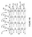
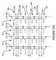
- FIGS. 13A , 13 B, 14 A and 14 Billustrate a memory array including a plurality of memory cells having a separate source line array that define a particular row of memory cells, and exemplary writing and/or programming techniques (including exemplary programming voltage values), according to another aspect of the present invention
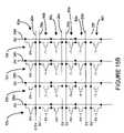
- FIGS. 15A and 15Billustrate read operations, including exemplary read operation voltage values, according to an embodiment of the present invention, for the memory array of FIGS. 13A , 13 B, 14 A and 14 B;
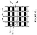
- FIG. 16illustrates an exemplary layout of the memory array of FIGS. 13A , 13 B, 14 A and 14 B;
- FIGS. 17 and 18illustrate another memory array architecture including a plurality of memory cells having a common source line array, and writing and/or programming techniques (including exemplary programming voltage values), according to another aspect of the present invention
- FIG. 19illustrates exemplary read operation voltage values, according to an embodiment of the present invention, for the memory array of FIGS. 17 and 18 ;
- FIG. 20illustrates an exemplary layout of the memory array of FIGS. 17 and 18 ;
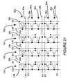
- FIG. 21illustrates a memory array including a plurality of memory cells having a separate source line array (that define a particular row of memory cells) and gates lines that are parallel to associated bit lines, and exemplary writing and/or programming techniques (including exemplary programming voltage values), according to another aspect of the present invention
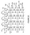
- FIG. 22illustrates exemplary read operation voltage values, according to an embodiment of the present invention, for the memory array of FIG. 21 ;
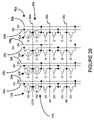
- FIG. 23illustrates an exemplary layout of the memory array of FIGS. 21 and 22 ;
- FIGS. 24 and 25illustrate another memory array architecture including a plurality of memory cells having a common source line array, and writing and/or programming techniques (including exemplary programming voltage values), according to another aspect of the present invention
- FIG. 26illustrates exemplary read operation voltage values, according to an embodiment of the present invention, for a memory array of FIGS. 25 and 26 ;
- FIG. 27illustrates an exemplary layout of the memory array of FIGS. 24 and 25 ;
- FIG. 28illustrates an exemplary configuration of a dual-port or a multi-port memory cell, according to another aspect of the present invention.
- FIG. 29illustrates an exemplary layout of the dual-port or a multi-port memory cell of FIG. 28 .
- the present inventionis directed to a memory device and technique of reading data from and writing data into memory cells of the memory device.
- the memory device and technique for operating that devicethat minimizes, reduces and/or eliminates the debilitating affects of the charge pumping phenomenon.
- This embodiment of the present inventionemploys control signals that minimize, reduce and/or eliminate transitions of the amplitudes and/or polarities.
- transistor 14(a 0.25 micron N-channel MOSFET DRAM cell) may be operated using the exemplary voltage values.
- a write logic low (binary data state “0”) operationin one exemplary embodiment, may be written by applying a word line (i.e., gate bias) voltage of 2.9V, and the bit line (here, a drain bias) voltage of 2.3V. In this operation, the source line voltage is maintained at 0V. Under these conditions, the junction between body region 18 and source region 20 is forward biased, and excess holes are removed from body region 18 into source region 20 .
- a voltage of 0.6Vis applied to gate 16 (i.e., the gate bias is held at 0.6V) and a voltage of 2.3V is applied to drain 22 .
- an electric current between source region 20 and drain region 22providing impact ionization in body region 18 , which in turn generates excess majority carriers (holes) in body region 18 .
- the gate voltage of unselected cellsis kept at 0V. It is found that these exemplary voltages avoid strong accumulation of holes at the interface of gate oxide 32 and floating body region 18 wherein minority carriers 34 have a tendency to be “trapped” by or in defects within the semiconductor. In this way, disturbance of data caused by charge pumping is suppressed, reduced, minimized and/or eliminated.
- transistor 14(a 0.25 micron N-channel MOSFET DRAM cell) may be operated using the exemplary voltage values indicated.
- a logic highbinary data state “1”
- a strong accumulation of majority carriers at the interface of gate oxide 32 and floating body region 18is required.
- a voltage of ⁇ 1.7Vis applied to gate 16 and a voltage of 1.7V is applied to drain region 22 to provide the strong accumulation of majority carrier at the interface of gate oxide 32 and floating body region 18 .
- These control signalscause deformation of the valence and conduction bands at the interface between body region 18 and source region 20 .
- an inversion channelis created at the interface of gate oxide 32 and floating body region 18 . This may be achieved by applying a voltage of 0V to gate 16 and drain region 22 (i.e., a gate bias of 0V) and a voltage of ⁇ 0.5V to source region 20 .
- transistor 14(a 0.13 micron technology DRAM cell) may be programmed and/or operated using the exemplary voltages indicated.
- the voltages set forth in FIG. 6represent “ideal” conditions, in which the application of the voltage pulses does not disturb the data stored within the cell.
- the cellsare arranged in matrices in which some cells are accessed when others remain un-accessed, and column and row decoding are therefore necessary to enable the matrices to function. This results in voltage levels differing from the levels being applied during write, read and hold operations (in practice, all of the cells that share either the same column or row with the addressed memory cell), as a consequence of which disturbance of the data stored within those cells may occur.
- FIGS. 1 and 7An example of this is shown in FIGS. 1 and 7 , in which data state “0” is being written to memory cell 12 at the intersection of the selected word line and bit line. Since all cells in the same column of FIG. 1 share the same gate voltage and all cells in the same row as FIG. 7 share the same drain voltage, voltages different from the “ideal” holding voltages are applied to those memory cells, as a result of which charge may leak from the floating body regions of those cells.
- the number of word line drivers and/or sense amplifiersare reduced and/or minimized.
- a column decoderis disposed or arranged between the bit lines and the sense amplifiers to reduce and/or minimize the number of sense amplifiers and, in conjunction, while only one cell in a block (typically 8 or 16) is read.
- the memory cell on a column defined by an internal counter (for example, among 8 or 16) and on a row defined by user addressesis read and thereafter, refreshed. That cell then is available for user access (via read or write operation) at the same row and column defined by the user addresses.
- the variations or swings of the amplitude, as well as the polarity, of the gate voltagesare reduced and/or minimized in number and rising/falling edges.
- a read or write operation of a predetermined memory cellmay occur prior to the refresh operation. (See, for example, FIG. 9 ).
- the semiconductor DRAM memory device of this aspect of the present inventionincludes a plurality of matrices 40 a–n , each including a plurality of memory cells 12 (comprised of transistors 14 ).
- the memory cells 12are arranged in arrays having rows and columns, which may be addressed by content address memory (CAM) 42 and column refresh counter 44 .
- CAMcontent address memory
- column refresh counter 44The column address output from column refresh counter 44 is applied to column address multiplexer 46 .
- the column address multiplexer 46receives the refresh address and the user address and provides one of the addresses to a column multiplexer 48 to select one of, for example, eight or sixteen bit lines (columns) 28 a.
- memory cell 12 at the intersection of a given or selected row and a given or selected columnis addressed by applying a signal on row address bus 50 to all of the interconnected gates of the row and a signal on column address bus 52 to all of the interconnected drains of the column.
- the row to be refreshedis identified by row refresh counter 54 , which is gated, via row address multiplexer 56 , with a row address from user address bus 58 .
- the column refresh counter 44supplies a column address of a column to be refreshed.
- the column addressis gated, via column address multiplexer 46 , with a column address from user address bus 58 .
- the column refresh counter 44may then increment in response to the same row being chosen, as a result of which the columns are sequentially addressed for each row, regardless of the order in which the rows are addressed. This provides the advantage of minimizing the risk that a memory cell 12 fails to be refreshed within the appropriate period.
- the column addressesare received from row refresh counter 44 or from user address bus 58 , and when, for example, the device (or portion thereof) is idle, the row addresses are provided by row refresh counter 54 .
- the refresh technique and circuitry of FIG. 11may be used with several arrays in parallel, as a result of which the number of sense amplifier 60 may be reduced and/or minimized (as is the area required for such circuitry on the die).
- the signal on WLDPW line 62provides a power supply voltage to word line drivers 62 a–x , according to the phase in the cycle waveform.
- the column multiplexer 48addresses the column (and therefore the selected memory cell) to be refreshed, and the data in the selected memory cell is read by sense amplifier 60 , the result being output (i.e., DATA signal) on signal line 66 .
- the write conditions applied to the word lineare as follows: During write “1” condition, if the DATA signal is “1”, XNOR logic gate 68 outputs, on signal line 68 , a logic high (i.e., binary “1”) which is amplified by write amplifier 72 and then applied to the selected memory cell in order to restore the data state in the selected memory cell. If the DATA signal is “0”, a logic low (i.e., “0”) is applied to the bit line, which represents a holding condition.
- the XNOR logic gate 68While writing data state “0”, on the other hand, if the DATA signal is “0”, the XNOR logic gate 68 outputs a logic high (i.e., binary “1”), which is amplified by write amplifier 72 and then applied to the memory cell to restore its data. If the DATA signal is “1”, a “0” is applied to the bit line, which again represents a holding condition.
- a two-step write operationmay be employed to program memory cell 12 with little to no disturbance to adjacent and/or neighboring cells (i.e., cells that share source lines, drain lines and/or gate lines).
- an entire row of memory cellsmay first be written to the same logic state and thereafter, individual bits are written to the opposite state in accordance with a desired data state (i.e., the individual bits are written to another state to reflect a desired data state).
- write techniquemay be implemented where memory cells 12 a–d of each row 80 a–f of transistors have a dedicated source line to minimize, reduce and/or eliminate disturbance on adjacent rows (for example, row 80 b versus row 80 c ).
- a given row 80 a–fmay be written to by applying a clear operation followed by a selective write operation.
- a plurality of memory cells 100having gates that are connected to a common gate line, are arranged to form row 80 a .
- Exemplary voltages that implement a clear operation for row 80 a and maintain the remaining portion of the array (i.e., rows 80 b–f ) in a fixed state (i.e., unchanged in response to the clear operation)are indicated in FIGS. 13A and 13B .
- the same logic statefor example, logic high or binary “1” is stored in memory cells 12 a–d of row 80 a . In this way, the state of memory cells 12 a–d are “cleared”.
- individual transistors of memory cells 12 a–d of row 80 aare written to a particular, desired and/or predetermined logic state (see, for example, FIGS. 14A and 14B ) in order to store the particular, desired and/or predetermined logic state in memory cells 12 a–d .
- memory cells 12 a–dare set to logic high (binary “1”) by the clear operation, and then memory cells 12 b and 12 d are written to logic low (binary “0”).
- the logic state of memory cells 12 a and 12 cremains logic high during the write operation (via applying an inhibit voltage to the associated bit lines 28 a and 28 c ( FIG. 14A ).
- memory cells 12 a–dare cleared to logic high (binary “1”) and then memory cells 12 a and 12 d are written to logic low (binary “0”).
- Memory cells 12 b and 12 cremain logic high via a write inhibit voltage applied to associated bit lines 28 b and 28 c.
- the datamay be read from memory cells 12 a–d of row 80 b by applying the exemplary voltages indicated.
- An exemplary holding voltage for the remaining portion of the arrayis also indicated.
- the holding voltage/signalmaintains the unselected portion of the array in a fixed state (i.e., unchanged in response to the read operation).
- the exemplary read and holding voltages of FIGS. 15A and 15Bmay avoid, reduce and/or minimize charge pumping disturb.
- the first step of the write operationclears the memory cells having a common source line and the second step writes or stores new data or the previous data (in the event that the data did not change).
- Array architectures employing this write operation techniquemay have an advantage that the unselected memory cells of the array are not “disturbed” (or experience little and/or negligible disturbance) because “high” voltages are applied in the row direction (i.e., on source lines 26 ) but not in the column direction (i.e., on the drain or bit lines 28 ).
- This write techniquemay be performed as a page mode write where the page is first “cleared” and then individual bytes (or bits) in a page are written to a new state.
- FIGS. 13A , 13 B, 14 A, 14 B, 15 A and 15 Bmay be implemented in conjunction with the embodiments of the device of FIGS. 11 and 12 .
- those discussionswill not be repeated.
- FIGS. 17–20illustrate another memory array architecture in which a plurality of memory cells “share” a source line and employ the two-step write technique that may eliminate, minimize and/or reduce disturbance to memory cells when reading from and/or writing to adjacent memory cells.
- a given rowmay be written to by applying suitable voltages to implement a clear operation ( FIG. 17 ) followed by a selective write operation ( FIG. 18 ).
- a write inhibit signalis applied to the gates of memory cells that share a source line 26 (for example, a write inhibit signal may be applied to the gates of the memory cell of row 80 b ).
- any disturbance on unselected, adjacent row 80 bmay avoid, reduce and/or minimize by biasing word line 24 b to an intermediate value that balances write logic low (i.e., write “0”) and write logic high (i.e., write “1”) operation.
- exemplary voltages that implement a clear operation for row 80 a and maintain the neighboring memory cells (for example, memory cells of row 80 b ) remaining portion of the array in a fixed state (i.e., unchanged in response to the clear operation)are indicated in FIG. 17 .
- the memory cells 12 a–d of row 80 aare written to a particular, desired and/or predetermined logic state (see, for example, FIG. 18 (write “0”) in memory cell 12 a and memory cell 12 d and (write “1”) in memory cell 12 b and memory cell 12 c ) in order to store a particular, desired and/or predetermined logic state of memory cell 12 .
- the datamay be read from memory cells 12 a–d of row 80 a by applying the exemplary voltages indicated.
- an exemplary holding voltage for the remaining portion of the arrayis also indicated.
- the holding voltage/signalmaintains the unselected portion of the array in a fixed state (i.e., unchanged in response to the read or write operation).
- FIGS. 17–20may be implemented in conjunction with the embodiments of the device of FIGS. 11 and 12 .
- FIGS. 11 and 12For the sake of brevity, those discussions will not be repeated.
- FIGS. 21–23Another memory array architecture that may employ a one-step write technique that eliminates, minimizes and/or reduces disturbance to memory cells when reading from and/or writing to adjacent memory cells is illustrated in FIGS. 21–23 .
- source lines 26are separated for each row 80 a–e .
- word lines 24 a–dare arranged parallel to associated bit lines 28 a–d , respectively.
- a given rowmay be written to by applying suitable voltages to directly implement a write operation (see, memory cells 12 a–d of row 80 a ).
- a write inhibit signalis applied to source lines 26 b–e of rows 80 b–e , respectively.
- Exemplary voltages that implement the write operation (for memory cells 12 a–d ) and the inhibit state (for the memory cells of rows 80 b–e )are indicated in FIG. 21 .
- the memory cells 12 a and 12 d of row 80 aare maintained and/or written to a particular, desired and/or predetermined logic state (here, write “1”) and memory cells 12 b and 12 c are written to a different desired and/or predetermined logic state (here, write “0”).
- the datamay be read from memory cell 12 a of row 80 a by applying the exemplary voltages indicated.
- an exemplary read inhibit voltage for the remaining portion of the arrayis also indicated.
- the read inhibit voltage/signalmaintains the unselected portion of the array in a fixed state (i.e., unchanged in response to the read operation).
- FIGS. 21–23may be implemented in conjunction with the embodiments of the device of FIGS. 11 and 12 . For the sake of brevity, those discussions will not be repeated.
- FIGS. 24–27Another memory array architecture that may employ the two-step write technique that eliminates, minimizes and/or reduces disturbance to memory cells when reading from and/or writing to adjacent memory cells is illustrated in FIGS. 24–27 .
- the source linesare shared but bit lines are separated so each memory cell on either side of a source line, for example memory cells 12 , has a dedicated bit line.
- the gates of transistors 12 a and 12 emay be connected together at the array boundary.
- memory cells 12 a and 12 eare located on separate rows with the gates of each transistor 12 a and 12 e connected at, for example, the array boundary.
- a given pair of rowsmay be written to by applying suitable voltage to implement a clear operation ( FIG. 24 ) followed by a selective write operation ( FIG. 25 ).
- the pair of rows(for example, rows 80 a and 80 b ) corresponding to memory cells 12 a and 12 e , on either side of a common source line, are written and read ( FIG. 26 ) simultaneously.
- FIGS. 24–27may be implemented in conjunction with the embodiments of the device of FIGS. 11 and 12 .
- those discussionswill not be repeated.
- the illustrated voltage levels to implement the write and read operationsare exemplary.
- the indicated voltage levelsmay be relative or absolute. That is, for example, a logic low may be written into transistor 102 a (see, for example, FIG. 13A ) using the voltages indicated therein.
- the voltages indicatedmay be relative in that each voltage level, for example, may be increased or decreased by a given voltage amount (for example, each voltage may be increased by 0.25 volts).
- the inventions(and embodiments thereof, described herein are entirely applicable to P-channel transistors.
- majority carriers 30 in body region 18are electrons and minority carriers 34 are holes.
- the memory arrays of matrices 40 a–nmay be comprised of N-channel, P-channel and/or both types of transistors.
- the circuitry that is peripheral to the memory arraymay include P-channel and/or N-channel type transistors, including transistors like transistor 14 .
- memory cell(s) 12may also employ the structure, features, attributes, architectures, configurations, materials, techniques and advantages described and illustrated in non-provisional patent application entitled “Semiconductor Device”, which was filed on Feb. 18, 2004, by Fazan and Okhonin, and assigned Ser. No. 10/487,157 (hereinafter “Semiconductor Device Patent Application”).
- semiconductor Device Patent ApplicationThe entire contents of the Semiconductor Device Patent Application, including, for example, the inventions, features, attributes, architectures, configurations, materials, techniques and advantages described and illustrated therein, are hereby incorporated by reference herein.
- a dual port memory cell 12 amay include transistors 14 a and 14 b .
- a dual port memory arraymay include a plurality of dual port memory cells 12 arranged, for example, in a matrix of rows and columns. The data state defined by the amount of carriers in the common electrically floating body region 18 is common to the two transistors 14 a and 14 b.
- the read and write access operationsmay be performed independently for transistors 14 a or 14 b , using the respective independent word lines 24 , source line 26 and bit lines 28 .
- source line 26is common to the transistors 14 a and 14 b of memory cell 12 a .
- the source regions of transistors 14 a and 14 bmay be connected to separate source lines.
- dual port memory cell 12 aincludes a P+ floating body node 18 that “connects” a P ⁇ floating body region under gate 24 m of transistor 14 a with a P ⁇ floating body region under gate 24 n of transistor 14 b .
- the gates 24 m and 24 nare connected to word lines 24 m and 24 n , respectively.
- the source regions 20 a and 20 bare connected to respective source lines.
- the drain regions 22 a and 22 bare connected to drain lines.
- majority carriers in body region 18are electrons, and minority carriers are holes.
Landscapes
- Engineering & Computer Science (AREA)
- Microelectronics & Electronic Packaging (AREA)
- Computer Hardware Design (AREA)
- Manufacturing & Machinery (AREA)
- Dram (AREA)
- Semiconductor Memories (AREA)
Abstract
Description
Claims (23)
Priority Applications (3)
| Application Number | Priority Date | Filing Date | Title |
|---|---|---|---|
| US11/079,590US7187581B2 (en) | 2003-05-13 | 2005-03-14 | Semiconductor memory device and method of operating same |
| US11/713,284US7359229B2 (en) | 2003-05-13 | 2007-03-02 | Semiconductor memory device and method of operating same |
| US12/082,020US7733693B2 (en) | 2003-05-13 | 2008-04-08 | Semiconductor memory device and method of operating same |
Applications Claiming Priority (4)
| Application Number | Priority Date | Filing Date | Title |
|---|---|---|---|
| US47038403P | 2003-05-13 | 2003-05-13 | |
| US47031803P | 2003-05-13 | 2003-05-13 | |
| US10/840,009US20040228168A1 (en) | 2003-05-13 | 2004-05-06 | Semiconductor memory device and method of operating same |
| US11/079,590US7187581B2 (en) | 2003-05-13 | 2005-03-14 | Semiconductor memory device and method of operating same |
Related Parent Applications (1)
| Application Number | Title | Priority Date | Filing Date |
|---|---|---|---|
| US10/840,009DivisionUS20040228168A1 (en) | 2003-05-13 | 2004-05-06 | Semiconductor memory device and method of operating same |
Related Child Applications (1)
| Application Number | Title | Priority Date | Filing Date |
|---|---|---|---|
| US11/713,284DivisionUS7359229B2 (en) | 2003-05-13 | 2007-03-02 | Semiconductor memory device and method of operating same |
Publications (2)
| Publication Number | Publication Date |
|---|---|
| US20050157580A1 US20050157580A1 (en) | 2005-07-21 |
| US7187581B2true US7187581B2 (en) | 2007-03-06 |
Family
ID=33425221
Family Applications (5)
| Application Number | Title | Priority Date | Filing Date |
|---|---|---|---|
| US10/840,009AbandonedUS20040228168A1 (en) | 2003-05-13 | 2004-05-06 | Semiconductor memory device and method of operating same |
| US11/079,590Expired - LifetimeUS7187581B2 (en) | 2003-05-13 | 2005-03-14 | Semiconductor memory device and method of operating same |
| US11/096,970Expired - LifetimeUS7085156B2 (en) | 2003-05-13 | 2005-04-01 | Semiconductor memory device and method of operating same |
| US11/713,284Expired - LifetimeUS7359229B2 (en) | 2003-05-13 | 2007-03-02 | Semiconductor memory device and method of operating same |
| US12/082,020Expired - LifetimeUS7733693B2 (en) | 2003-05-13 | 2008-04-08 | Semiconductor memory device and method of operating same |
Family Applications Before (1)
| Application Number | Title | Priority Date | Filing Date |
|---|---|---|---|
| US10/840,009AbandonedUS20040228168A1 (en) | 2003-05-13 | 2004-05-06 | Semiconductor memory device and method of operating same |
Family Applications After (3)
| Application Number | Title | Priority Date | Filing Date |
|---|---|---|---|
| US11/096,970Expired - LifetimeUS7085156B2 (en) | 2003-05-13 | 2005-04-01 | Semiconductor memory device and method of operating same |
| US11/713,284Expired - LifetimeUS7359229B2 (en) | 2003-05-13 | 2007-03-02 | Semiconductor memory device and method of operating same |
| US12/082,020Expired - LifetimeUS7733693B2 (en) | 2003-05-13 | 2008-04-08 | Semiconductor memory device and method of operating same |
Country Status (4)
| Country | Link |
|---|---|
| US (5) | US20040228168A1 (en) |
| EP (1) | EP1623430A4 (en) |
| JP (1) | JP5549899B2 (en) |
| WO (1) | WO2004102576A2 (en) |
Cited By (53)
| Publication number | Priority date | Publication date | Assignee | Title |
|---|---|---|---|---|
| US20070257291A1 (en)* | 2006-05-02 | 2007-11-08 | Serguei Okhonin | Semiconductor memory cell and array using punch-through to program and read same |
| US20070297252A1 (en)* | 2006-06-26 | 2007-12-27 | Anant Pratap Singh | Integrated circuit having memory array including ECC and/or column redundancy, and method of programming, controlling and/or operating same |
| US20080180995A1 (en)* | 2007-01-26 | 2008-07-31 | Serguei Okhonin | Semiconductor Device With Electrically Floating Body |
| US20080237714A1 (en)* | 2007-03-29 | 2008-10-02 | Pierre Fazan | Manufacturing Process for Zero-Capacitor Random Access Memory Circuits |
| US20080298139A1 (en)* | 2007-05-30 | 2008-12-04 | David Fisch | Integrated circuit having voltage generation circuitry for memory cell array, and method of operating and /or controlling same |
| US20090022003A1 (en)* | 2007-07-20 | 2009-01-22 | Song Ki-Whan | Memory cell structures, memory arrays, memory devices, memory controllers, and memory systems, and methods of manufacturing and operating the same |
| US20090034338A1 (en)* | 2007-08-01 | 2009-02-05 | Sung-Wei Lin | System and method for reading memory |
| US20090078999A1 (en)* | 2007-09-20 | 2009-03-26 | Anderson Brent A | Semiconductor device structures with floating body charge storage and methods for forming such semiconductor device structures. |
| WO2009039169A1 (en)* | 2007-09-17 | 2009-03-26 | Innovative Silicon S.A. | Refreshing data of memory cells with electrically floating body transistors |
| US20090097332A1 (en)* | 2007-10-10 | 2009-04-16 | Samsung Electronics Co., Ltd. | Semiconductor memory device |
| US20090141550A1 (en)* | 2006-04-07 | 2009-06-04 | Eric Carman | Memory Array Having a Programmable Word Length, and Method of Operating Same |
| US20090146219A1 (en)* | 2007-12-11 | 2009-06-11 | Danngis Liu | Integrated circuit having memory cell array, and method of manufacturing same |
| US20090200612A1 (en)* | 2008-02-08 | 2009-08-13 | Viktor Koldiaev | Integrated Circuit Having Memory Cells Including Gate Material Having High Work Function, and Method of Manufacturing Same |
| US20090212362A1 (en)* | 2008-02-25 | 2009-08-27 | International Business Machines Corporation | Soi field effect transistor with a back gate for modulating a floating body |
| US20090231898A1 (en)* | 2006-07-11 | 2009-09-17 | David Fisch | Integrated Circuit Including Memory Array Having a Segmented Bit Line Architecture and Method of Controlling and/or Operating Same |
| US20090251958A1 (en)* | 2008-04-04 | 2009-10-08 | Philippe Bauser | Read circuitry for an integrated circuit having memory cells and/or a memory cell array, and method of operating same |
| US20090278194A1 (en)* | 2008-05-06 | 2009-11-12 | Nam-Kyun Tak | Capacitorless one-transistor semiconductor memory device having improved data retention abilities and operation characteristics |
| US20100075471A1 (en)* | 2008-09-25 | 2010-03-25 | Innovative Silicon Isi Sa | Recessed Gate Silicon-On-Insulator Floating Body Device With Self-Aligned Lateral Isolation |
| US20100085806A1 (en)* | 2008-10-02 | 2010-04-08 | Ping Wang | Techniques for reducing a voltage swing |
| US20100091586A1 (en)* | 2008-10-15 | 2010-04-15 | Innovative Silicon Isi Sa | Techniques for simultaneously driving a plurality of source lines |
| US20100110816A1 (en)* | 2008-11-05 | 2010-05-06 | Innovative Silicon Isi Sa | Techniques for block refreshing a semiconductor memory device |
| US7733693B2 (en) | 2003-05-13 | 2010-06-08 | Innovative Silicon Isi Sa | Semiconductor memory device and method of operating same |
| US20100149886A1 (en)* | 2008-12-17 | 2010-06-17 | Samsung Electronics Co., Ltd. | Semiconductor memory device and method for operating the same |
| US20100159650A1 (en)* | 2008-12-18 | 2010-06-24 | Song Ho-Ju | Methods of fabricating semiconductor device having capacitorless one-transistor memory cell |
| US20100210075A1 (en)* | 2009-02-18 | 2010-08-19 | Innovative Silicon Isi Sa | Techniques for providing a source line plane |
| US20100213521A1 (en)* | 2009-02-26 | 2010-08-26 | Sanghun Jeon | Semiconductor devices and methods of forming semiconductor devices |
| US20100224924A1 (en)* | 2009-03-04 | 2010-09-09 | Innovative Silicon Isi Sa | Techniques for forming a contact to a buried diffusion layer in a semiconductor memory device |
| US20100259964A1 (en)* | 2009-03-31 | 2010-10-14 | Innovative Silicon Isi Sa | Techniques for providing a semiconductor memory device |
| US20100260003A1 (en)* | 2009-04-14 | 2010-10-14 | Young Hoon Oh | Semiconductor memory apparatus and refresh control method of the same |
| US20100271858A1 (en)* | 2009-04-27 | 2010-10-28 | Innovative Silicon Isi Sa | Techniques for providing a direct injection semiconductor memory device having ganged carrier injection lines |
| US20100277982A1 (en)* | 2009-04-30 | 2010-11-04 | Innovative Silicon Isi Sa | Semiconductor device with floating gate and electrically floating body |
| US20110007578A1 (en)* | 2009-07-10 | 2011-01-13 | Innovative Silicon Isi Sa | Techniques for providing a semiconductor memory device |
| US20110019481A1 (en)* | 2009-07-27 | 2011-01-27 | Innovative Silicon Isi Sa | Techniques for providing a direct injection semiconductor memory device |
| US20110058436A1 (en)* | 2009-09-04 | 2011-03-10 | Innovative Silicon Isi Sa | Techniques for sensing a semiconductor memory device |
| US7924644B2 (en) | 2008-01-03 | 2011-04-12 | Samsung Electronics Co., Ltd. | Semiconductor memory device including floating body transistor memory cell array and method of operating the same |
| US20110141836A1 (en)* | 2009-12-16 | 2011-06-16 | Innovative Silicon Isi Sa | Techniques for reducing impact of array disturbs in a semiconductor memory device |
| US20110199848A1 (en)* | 2010-02-12 | 2011-08-18 | Innovative Silicon Isi Sa | Techniques for controlling a semiconductor memory device |
| US8014195B2 (en) | 2008-02-06 | 2011-09-06 | Micron Technology, Inc. | Single transistor memory cell |
| US20110216617A1 (en)* | 2010-03-04 | 2011-09-08 | Innovative Silicon Isi Sa | Techniques for sensing a semiconductor memory device |
| US20110216608A1 (en)* | 2010-03-05 | 2011-09-08 | Innovative Silicon Isi Sa | Techniques for reading from and/or writing to a semiconductor memory device |
| US20110216605A1 (en)* | 2010-03-04 | 2011-09-08 | Innovative Silicon Isi Sa | Techniques for providing a semiconductor memory device having hierarchical bit lines |
| US8085594B2 (en) | 2007-06-01 | 2011-12-27 | Micron Technology, Inc. | Reading technique for memory cell with electrically floating body transistor |
| WO2011140033A3 (en)* | 2010-05-06 | 2012-01-19 | Micron Technology, Inc. | Techniques for refreshing a semiconductor memory device |
| US8174881B2 (en) | 2009-11-24 | 2012-05-08 | Micron Technology, Inc. | Techniques for reducing disturbance in a semiconductor device |
| US8213226B2 (en) | 2008-12-05 | 2012-07-03 | Micron Technology, Inc. | Vertical transistor memory cell and array |
| US8498157B2 (en) | 2009-05-22 | 2013-07-30 | Micron Technology, Inc. | Techniques for providing a direct injection semiconductor memory device |
| US8531878B2 (en) | 2011-05-17 | 2013-09-10 | Micron Technology, Inc. | Techniques for providing a semiconductor memory device |
| US8536628B2 (en) | 2007-11-29 | 2013-09-17 | Micron Technology, Inc. | Integrated circuit having memory cell array including barriers, and method of manufacturing same |
| US8547738B2 (en) | 2010-03-15 | 2013-10-01 | Micron Technology, Inc. | Techniques for providing a semiconductor memory device |
| US8773933B2 (en) | 2012-03-16 | 2014-07-08 | Micron Technology, Inc. | Techniques for accessing memory cells |
| US8873283B2 (en) | 2005-09-07 | 2014-10-28 | Micron Technology, Inc. | Memory cell and memory cell array having an electrically floating body transistor, and methods of operating same |
| US9559216B2 (en) | 2011-06-06 | 2017-01-31 | Micron Technology, Inc. | Semiconductor memory device and method for biasing same |
| US11063048B2 (en)* | 2010-11-16 | 2021-07-13 | Zeno Semiconductor, Inc. | Dual-port semiconductor memory and first in first out (FIFO) memory having electrically floating body transistor |
Families Citing this family (81)
| Publication number | Priority date | Publication date | Assignee | Title |
|---|---|---|---|---|
| US7085153B2 (en)* | 2003-05-13 | 2006-08-01 | Innovative Silicon S.A. | Semiconductor memory cell, array, architecture and device, and method of operating same |
| KR100742063B1 (en)* | 2003-05-26 | 2007-07-23 | 가시오게산키 가부시키가이샤 | Electric current generation supply circuit and display device |
| JP4304585B2 (en)* | 2003-06-30 | 2009-07-29 | カシオ計算機株式会社 | CURRENT GENERATION SUPPLY CIRCUIT, CONTROL METHOD THEREOF, AND DISPLAY DEVICE PROVIDED WITH THE CURRENT GENERATION SUPPLY CIRCUIT |
| JP4103079B2 (en)* | 2003-07-16 | 2008-06-18 | カシオ計算機株式会社 | CURRENT GENERATION SUPPLY CIRCUIT, ITS CONTROL METHOD, AND DISPLAY DEVICE PROVIDED WITH CURRENT GENERATION SUPPLY CIRCUIT |
| US7301803B2 (en) | 2004-12-22 | 2007-11-27 | Innovative Silicon S.A. | Bipolar reading technique for a memory cell having an electrically floating body transistor |
| US7317641B2 (en)* | 2005-06-20 | 2008-01-08 | Sandisk Corporation | Volatile memory cell two-pass writing method |
| US7274618B2 (en)* | 2005-06-24 | 2007-09-25 | Monolithic System Technology, Inc. | Word line driver for DRAM embedded in a logic process |
| US7499307B2 (en)* | 2005-06-24 | 2009-03-03 | Mosys, Inc. | Scalable embedded DRAM array |
| US7355916B2 (en) | 2005-09-19 | 2008-04-08 | Innovative Silicon S.A. | Method and circuitry to generate a reference current for reading a memory cell, and device implementing same |
| WO2007052649A1 (en)* | 2005-10-31 | 2007-05-10 | Sharp Kabushiki Kaisha | Radio transmitter, radio communication system, and radio transmission method |
| JP4373972B2 (en)* | 2005-11-14 | 2009-11-25 | 東芝メモリシステムズ株式会社 | Semiconductor memory device |
| FR2894708A1 (en)* | 2005-12-08 | 2007-06-15 | St Microelectronics Sa | MEMORY MEMORY CELL WITH MOS BODY TRANSISTOR |
| US7542345B2 (en) | 2006-02-16 | 2009-06-02 | Innovative Silicon Isi Sa | Multi-bit memory cell having electrically floating body transistor, and method of programming and reading same |
| US7606098B2 (en) | 2006-04-18 | 2009-10-20 | Innovative Silicon Isi Sa | Semiconductor memory array architecture with grouped memory cells, and method of controlling same |
| US7499352B2 (en)* | 2006-05-19 | 2009-03-03 | Innovative Silicon Isi Sa | Integrated circuit having memory array including row redundancy, and method of programming, controlling and/or operating same |
| US7608898B2 (en)* | 2006-10-31 | 2009-10-27 | Freescale Semiconductor, Inc. | One transistor DRAM cell structure |
| US8194451B2 (en) | 2007-11-29 | 2012-06-05 | Zeno Semiconductor, Inc. | Memory cells, memory cell arrays, methods of using and methods of making |
| US8159868B2 (en)* | 2008-08-22 | 2012-04-17 | Zeno Semiconductor, Inc. | Semiconductor memory having both volatile and non-volatile functionality including resistance change material and method of operating |
| US8547756B2 (en) | 2010-10-04 | 2013-10-01 | Zeno Semiconductor, Inc. | Semiconductor memory device having an electrically floating body transistor |
| US8077536B2 (en) | 2008-08-05 | 2011-12-13 | Zeno Semiconductor, Inc. | Method of operating semiconductor memory device with floating body transistor using silicon controlled rectifier principle |
| US9391079B2 (en) | 2007-11-29 | 2016-07-12 | Zeno Semiconductor, Inc. | Compact semiconductor memory device having reduced number of contacts, methods of operating and methods of making |
| US7760548B2 (en) | 2006-11-29 | 2010-07-20 | Yuniarto Widjaja | Semiconductor memory having both volatile and non-volatile functionality and method of operating |
| US9601493B2 (en) | 2006-11-29 | 2017-03-21 | Zeno Semiconductor, Inc | Compact semiconductor memory device having reduced number of contacts, methods of operating and methods of making |
| US8514622B2 (en) | 2007-11-29 | 2013-08-20 | Zeno Semiconductor, Inc. | Compact semiconductor memory device having reduced number of contacts, methods of operating and methods of making |
| US7724578B2 (en)* | 2006-12-15 | 2010-05-25 | Globalfoundries Inc. | Sensing device for floating body cell memory and method thereof |
| US7688660B2 (en)* | 2007-04-12 | 2010-03-30 | Qimonda Ag | Semiconductor device, an electronic device and a method for operating the same |
| US9230651B2 (en) | 2012-04-08 | 2016-01-05 | Zeno Semiconductor, Inc. | Memory device having electrically floating body transitor |
| EP2015362A1 (en) | 2007-06-04 | 2009-01-14 | STMicroelectronics (Crolles 2) SAS | Semiconductor array and manufacturing method thereof |
| JP2009032384A (en) | 2007-06-29 | 2009-02-12 | Toshiba Corp | Semiconductor memory device driving method and semiconductor memory device |
| JP5217042B2 (en)* | 2007-07-06 | 2013-06-19 | ルネサスエレクトロニクス株式会社 | Semiconductor memory device |
| US8059459B2 (en) | 2007-10-24 | 2011-11-15 | Zeno Semiconductor, Inc. | Semiconductor memory having both volatile and non-volatile functionality and method of operating |
| US8130547B2 (en) | 2007-11-29 | 2012-03-06 | Zeno Semiconductor, Inc. | Method of maintaining the state of semiconductor memory having electrically floating body transistor |
| US8264875B2 (en) | 2010-10-04 | 2012-09-11 | Zeno Semiconducor, Inc. | Semiconductor memory device having an electrically floating body transistor |
| US8130548B2 (en)* | 2007-11-29 | 2012-03-06 | Zeno Semiconductor, Inc. | Semiconductor memory having electrically floating body transistor |
| US8174886B2 (en) | 2007-11-29 | 2012-05-08 | Zeno Semiconductor, Inc. | Semiconductor memory having electrically floating body transistor |
| US10403361B2 (en) | 2007-11-29 | 2019-09-03 | Zeno Semiconductor, Inc. | Memory cells, memory cell arrays, methods of using and methods of making |
| KR101003115B1 (en)* | 2007-12-12 | 2010-12-21 | 주식회사 하이닉스반도체 | Semiconductor memory device with floating body capacitor and manufacturing method thereof |
| JP2009205724A (en)* | 2008-02-27 | 2009-09-10 | Toshiba Corp | Semiconductor memory device |
| US8014200B2 (en) | 2008-04-08 | 2011-09-06 | Zeno Semiconductor, Inc. | Semiconductor memory having volatile and multi-bit, non-volatile functionality and methods of operating |
| KR101442175B1 (en) | 2008-05-23 | 2014-09-18 | 삼성전자주식회사 | Semiconductor memory device and arrangement methode of memory cell array thereof |
| USRE47381E1 (en) | 2008-09-03 | 2019-05-07 | Zeno Semiconductor, Inc. | Forming semiconductor cells with regions of varying conductivity |
| JP4751432B2 (en)* | 2008-09-26 | 2011-08-17 | シャープ株式会社 | Semiconductor memory device |
| US8639874B2 (en)* | 2008-12-22 | 2014-01-28 | International Business Machines Corporation | Power management of a spare DRAM on a buffered DIMM by issuing a power on/off command to the DRAM device |
| US20100162037A1 (en)* | 2008-12-22 | 2010-06-24 | International Business Machines Corporation | Memory System having Spare Memory Devices Attached to a Local Interface Bus |
| US11908899B2 (en) | 2009-02-20 | 2024-02-20 | Zeno Semiconductor, Inc. | MOSFET and memory cell having improved drain current through back bias application |
| WO2016176248A1 (en) | 2015-04-29 | 2016-11-03 | Zeno Semiconductor, Inc. | A mosfet and memory cell having improved drain current through back bias application |
| IN2012DN06399A (en) | 2010-02-07 | 2015-10-02 | Zeno Semiconductor Inc | |
| US9922981B2 (en) | 2010-03-02 | 2018-03-20 | Zeno Semiconductor, Inc. | Compact semiconductor memory device having reduced number of contacts, methods of operating and methods of making |
| US8507966B2 (en)* | 2010-03-02 | 2013-08-13 | Micron Technology, Inc. | Semiconductor cells, arrays, devices and systems having a buried conductive line and methods for forming the same |
| US9608119B2 (en) | 2010-03-02 | 2017-03-28 | Micron Technology, Inc. | Semiconductor-metal-on-insulator structures, methods of forming such structures, and semiconductor devices including such structures |
| US10461084B2 (en) | 2010-03-02 | 2019-10-29 | Zeno Semiconductor, Inc. | Compact semiconductor memory device having reduced number of contacts, methods of operating and methods of making |
| US10340276B2 (en) | 2010-03-02 | 2019-07-02 | Zeno Semiconductor, Inc. | Method of maintaining the state of semiconductor memory having electrically floating body transistor |
| US8513722B2 (en) | 2010-03-02 | 2013-08-20 | Micron Technology, Inc. | Floating body cell structures, devices including same, and methods for forming same |
| US8288795B2 (en)* | 2010-03-02 | 2012-10-16 | Micron Technology, Inc. | Thyristor based memory cells, devices and systems including the same and methods for forming the same |
| US9646869B2 (en) | 2010-03-02 | 2017-05-09 | Micron Technology, Inc. | Semiconductor devices including a diode structure over a conductive strap and methods of forming such semiconductor devices |
| CN102376717B (en)* | 2010-08-05 | 2013-05-01 | 亿而得微电子股份有限公司 | EEPROM Array with Low Voltage Operation |
| US8305808B2 (en)* | 2010-08-12 | 2012-11-06 | Yield Microelectronics Corp. | Low-voltage EEPROM array |
| US8598621B2 (en) | 2011-02-11 | 2013-12-03 | Micron Technology, Inc. | Memory cells, memory arrays, methods of forming memory cells, and methods of forming a shared doped semiconductor region of a vertically oriented thyristor and a vertically oriented access transistor |
| US8952418B2 (en) | 2011-03-01 | 2015-02-10 | Micron Technology, Inc. | Gated bipolar junction transistors |
| US8519431B2 (en) | 2011-03-08 | 2013-08-27 | Micron Technology, Inc. | Thyristors |
| US8957458B2 (en) | 2011-03-24 | 2015-02-17 | Zeno Semiconductor, Inc. | Asymmetric semiconductor memory device having electrically floating body transistor |
| CN102867540A (en)* | 2011-07-05 | 2013-01-09 | 复旦大学 | Operation method for raising multiport multichannel floating body memory performance |
| US8772848B2 (en) | 2011-07-26 | 2014-07-08 | Micron Technology, Inc. | Circuit structures, memory circuitry, and methods |
| US20130033285A1 (en)* | 2011-08-02 | 2013-02-07 | Globalfoundries Inc. | Methods for reliability testing of semiconductor devices |
| US9025358B2 (en) | 2011-10-13 | 2015-05-05 | Zeno Semiconductor Inc | Semiconductor memory having both volatile and non-volatile functionality comprising resistive change material and method of operating |
| CN107331416B (en) | 2012-02-16 | 2020-11-10 | 芝诺半导体有限公司 | Memory cell including primary and secondary transistors |
| US11024352B2 (en) | 2012-04-10 | 2021-06-01 | Samsung Electronics Co., Ltd. | Memory system for access concentration decrease management and access concentration decrease method |
| US9208880B2 (en) | 2013-01-14 | 2015-12-08 | Zeno Semiconductor, Inc. | Content addressable memory device having electrically floating body transistor |
| US9029922B2 (en) | 2013-03-09 | 2015-05-12 | Zeno Semiconductor, Inc. | Memory device comprising electrically floating body transistor |
| US9275723B2 (en) | 2013-04-10 | 2016-03-01 | Zeno Semiconductor, Inc. | Scalable floating body memory cell for memory compilers and method of using floating body memories with memory compilers |
| US9368625B2 (en) | 2013-05-01 | 2016-06-14 | Zeno Semiconductor, Inc. | NAND string utilizing floating body memory cell |
| US9281022B2 (en) | 2013-07-10 | 2016-03-08 | Zeno Semiconductor, Inc. | Systems and methods for reducing standby power in floating body memory devices |
| US9524771B2 (en)* | 2013-07-12 | 2016-12-20 | Qualcomm Incorporated | DRAM sub-array level autonomic refresh memory controller optimization |
| US9548119B2 (en) | 2014-01-15 | 2017-01-17 | Zeno Semiconductor, Inc | Memory device comprising an electrically floating body transistor |
| US9496053B2 (en) | 2014-08-15 | 2016-11-15 | Zeno Semiconductor, Inc. | Memory device comprising electrically floating body transistor |
| US10553683B2 (en) | 2015-04-29 | 2020-02-04 | Zeno Semiconductor, Inc. | MOSFET and memory cell having improved drain current through back bias application |
| US10079301B2 (en) | 2016-11-01 | 2018-09-18 | Zeno Semiconductor, Inc. | Memory device comprising an electrically floating body transistor and methods of using |
| TWI787498B (en) | 2018-04-18 | 2022-12-21 | 美商季諾半導體股份有限公司 | A memory device comprising an electrically floating body transistor |
| US11600663B2 (en) | 2019-01-11 | 2023-03-07 | Zeno Semiconductor, Inc. | Memory cell and memory array select transistor |
| US12439611B2 (en) | 2019-03-12 | 2025-10-07 | Zeno Semiconductor, Inc. | Memory cell and memory array select transistor |
| US11889680B2 (en)* | 2020-08-28 | 2024-01-30 | Micron Technology, Inc. | Integrated assemblies and methods of forming integrated assemblies |
Citations (193)
| Publication number | Priority date | Publication date | Assignee | Title |
|---|---|---|---|---|
| US3439214A (en) | 1968-03-04 | 1969-04-15 | Fairchild Camera Instr Co | Beam-junction scan converter |
| FR2197494A5 (en) | 1972-08-25 | 1974-03-22 | Radiotechnique Compelec | |
| GB1414228A (en) | 1972-04-25 | 1975-11-19 | Ibm | Semiconductor storage devices |
| US3997799A (en) | 1975-09-15 | 1976-12-14 | Baker Roger T | Semiconductor-device for the storage of binary data |
| US4032947A (en) | 1971-10-20 | 1977-06-28 | Siemens Aktiengesellschaft | Controllable charge-coupled semiconductor device |
| US4250569A (en) | 1978-11-15 | 1981-02-10 | Fujitsu Limited | Semiconductor memory device |
| US4262340A (en) | 1978-11-14 | 1981-04-14 | Fujitsu Limited | Semiconductor memory device |
| US4298962A (en) | 1979-01-25 | 1981-11-03 | Nippon Electric Co., Ltd. | Memory |
| US4371955A (en) | 1979-02-22 | 1983-02-01 | Fujitsu Limited | Charge-pumping MOS FET memory device |
| EP0030856B1 (en) | 1979-12-13 | 1984-03-21 | Fujitsu Limited | Charge-pumping semiconductor memory cell comprising a charge-storage region and memory device using such a cell |
| US4527181A (en) | 1980-08-28 | 1985-07-02 | Fujitsu Limited | High density semiconductor memory array and method of making same |
| US4630089A (en) | 1983-09-27 | 1986-12-16 | Fujitsu Limited | Semiconductor memory device |
| JPS62272561A (en) | 1986-05-20 | 1987-11-26 | Seiko Epson Corp | 1 transistor memory cell |
| US4791610A (en) | 1985-05-24 | 1988-12-13 | Fujitsu Limited | Semiconductor memory device formed of a SOI-type transistor and a capacitor |
| EP0354348A2 (en) | 1988-08-10 | 1990-02-14 | International Business Machines Corporation | CMOS-transistor and one-capacitor dram cell and fabrication process therefor |
| JPH02294076A (en) | 1989-05-08 | 1990-12-05 | Hitachi Ltd | Semiconductor integrated circuit device |
| US4979014A (en) | 1987-08-10 | 1990-12-18 | Kabushiki Kaisha Toshiba | MOS transistor |
| EP0202515B1 (en) | 1982-11-04 | 1991-03-13 | Hitachi, Ltd. | Semiconductor memory |
| JPH03171768A (en) | 1989-11-30 | 1991-07-25 | Toshiba Corp | semiconductor storage device |
| EP0175378B1 (en) | 1984-09-21 | 1991-11-21 | Fujitsu Limited | Dynamic random access memory (dram) |
| EP0253631B1 (en) | 1986-07-14 | 1992-04-22 | Oki Electric Industry Company, Limited | Semiconductor memory device |
| US5144390A (en) | 1988-09-02 | 1992-09-01 | Texas Instruments Incorporated | Silicon-on insulator transistor with internal body node to source node connection |
| US5164805A (en) | 1988-08-22 | 1992-11-17 | Massachusetts Institute Of Technology | Near-intrinsic thin-film SOI FETS |
| EP0300157B1 (en) | 1987-07-20 | 1993-05-05 | International Business Machines Corporation | Vertical transistor capacitor memory cell structure and fabrication method therefor |
| US5258635A (en) | 1988-09-06 | 1993-11-02 | Kabushiki Kaisha Toshiba | MOS-type semiconductor integrated circuit device |
| EP0350057B1 (en) | 1988-07-07 | 1993-12-01 | Kabushiki Kaisha Toshiba | Semiconductor memory |
| EP0579566A2 (en) | 1992-06-17 | 1994-01-19 | International Business Machines Corporation | High-density dram structure on SOI |
| EP0362961B1 (en) | 1988-10-03 | 1994-02-16 | Interuniversitair Microelektronica Centrum Vzw | A method of operating a MOS-structure and MOS-structure therefor |
| EP0599506A1 (en) | 1992-11-27 | 1994-06-01 | International Business Machines Corporation | Semiconductor memory cell with SOI MOSFET |
| EP0359551B1 (en) | 1988-09-14 | 1994-12-28 | Kawasaki Steel Corporation | Semicoductor memory circuit |
| US5388068A (en) | 1990-05-02 | 1995-02-07 | Microelectronics & Computer Technology Corp. | Superconductor-semiconductor hybrid memory circuits with superconducting three-terminal switching devices |
| EP0366882B1 (en) | 1988-10-31 | 1995-05-24 | International Business Machines Corporation | An ultra dense DRAM cell array and its method of fabrication |
| EP0465961B1 (en) | 1990-07-09 | 1995-08-09 | Sony Corporation | Semiconductor device on a dielectric isolated substrate |
| US5446299A (en) | 1994-04-29 | 1995-08-29 | International Business Machines Corporation | Semiconductor random access memory cell on silicon-on-insulator with dual control gates |
| US5448513A (en) | 1993-12-02 | 1995-09-05 | Regents Of The University Of California | Capacitorless DRAM device on silicon-on-insulator substrate |
| EP0513923B1 (en) | 1991-05-15 | 1995-09-27 | Koninklijke Philips Electronics N.V. | Protected programmable transistor with reduced parasitic capacitances and method of fabrication |
| US5489792A (en) | 1994-04-07 | 1996-02-06 | Regents Of The University Of California | Silicon-on-insulator transistors having improved current characteristics and reduced electrostatic discharge susceptibility |
| EP0333426B1 (en) | 1988-03-15 | 1996-07-10 | Kabushiki Kaisha Toshiba | Dynamic RAM |
| JPH08213624A (en) | 1995-02-08 | 1996-08-20 | Fujitsu Ltd | Semiconductor memory device and operating method thereof |
| EP0727820A1 (en) | 1995-02-17 | 1996-08-21 | Hitachi, Ltd. | Semiconductor memory device and method of manufacturing the same |
| JPH08274277A (en) | 1995-03-31 | 1996-10-18 | Toyota Central Res & Dev Lab Inc | Semiconductor memory device and manufacturing method thereof |
| US5568356A (en) | 1995-04-18 | 1996-10-22 | Hughes Aircraft Company | Stacked module assembly including electrically interconnected switching module and plural electronic modules |
| EP0739097A2 (en) | 1995-04-21 | 1996-10-23 | Nippon Telegraph And Telephone Corporation | MOSFET circuit and CMOS logic circuit using the same |
| EP0694977A3 (en) | 1994-07-14 | 1996-11-06 | Nec Corp | SOI-type semiconductor device with suppression of extension of the depletion region |
| US5593912A (en) | 1994-10-06 | 1997-01-14 | International Business Machines Corporation | SOI trench DRAM cell for 256 MB DRAM and beyond |
| JPH0946686A (en) | 1995-07-25 | 1997-02-14 | Toshiba Corp | Transmitter / receiver in bidirectional CATV system |
| US5606188A (en) | 1995-04-26 | 1997-02-25 | International Business Machines Corporation | Fabrication process and structure for a contacted-body silicon-on-insulator dynamic random access memory |
| US5608250A (en) | 1993-11-29 | 1997-03-04 | Sgs-Thomson Microelectronics S.A. | Volatile memory cell with interface charge traps |
| EP0599368B1 (en) | 1992-11-17 | 1997-03-12 | Agfa-Gevaert N.V. | Thermal imaging method |
| JPH0982912A (en) | 1995-09-13 | 1997-03-28 | Toshiba Corp | Semiconductor memory device and manufacturing method thereof |
| EP0245515B1 (en) | 1985-11-20 | 1997-04-16 | Hitachi, Ltd. | Semiconductor device |
| US5627092A (en) | 1994-09-26 | 1997-05-06 | Siemens Aktiengesellschaft | Deep trench dram process on SOI for low leakage DRAM cell |
| US5631186A (en) | 1992-12-30 | 1997-05-20 | Samsung Electronics Co., Ltd. | Method for making a dynamic random access memory using silicon-on-insulator techniques |
| EP0788165A2 (en) | 1996-02-02 | 1997-08-06 | Siemens Aktiengesellschaft | Storage cell arrangement and method for making the same |
| US5696718A (en) | 1994-11-10 | 1997-12-09 | Commissariat A L'energie Atomique | Device having an electrically erasable non-volatile memory and process for producing such a device |
| EP0510607B1 (en) | 1991-04-23 | 1998-02-04 | Canon Kabushiki Kaisha | Semiconductor memory device |
| US5740099A (en) | 1995-02-07 | 1998-04-14 | Nec Corporation | Semiconductor memory device having peripheral circuit and interface circuit fabricated on bulk region out of silicon-on-insulator region for memory cells |
| US5778243A (en) | 1996-07-03 | 1998-07-07 | International Business Machines Corporation | Multi-threaded cell for a memory |
| US5780906A (en) | 1995-06-21 | 1998-07-14 | Micron Technology, Inc. | Static memory cell and method of manufacturing a static memory cell |
| US5784311A (en) | 1997-06-13 | 1998-07-21 | International Business Machines Corporation | Two-device memory cell on SOI for merged logic and memory applications |
| EP0858109A2 (en) | 1997-02-07 | 1998-08-12 | Nec Corporation | Semiconductor memory device and method for manufacturing thereof |
| EP0537677B1 (en) | 1991-10-16 | 1998-08-19 | Sony Corporation | Method of forming an SOI structure with a DRAM |
| EP0860878A2 (en) | 1997-02-20 | 1998-08-26 | Texas Instruments Incorporated | An integrated circuit with programmable elements |
| JPH10242470A (en) | 1997-02-28 | 1998-09-11 | Toshiba Corp | Semiconductor device and manufacturing method thereof |
| US5811283A (en) | 1996-08-13 | 1998-09-22 | United Microelectronics Corporation | Silicon on insulator (SOI) dram cell structure and process |
| EP0869511A2 (en) | 1997-04-02 | 1998-10-07 | Sony Corporation | Semiconductor memory cell and method of manufacturing the same |
| US5877978A (en) | 1996-03-04 | 1999-03-02 | Mitsubishi Denki Kabushiki Kaisha | Semiconductor memory device |
| US5877524A (en)* | 1995-06-15 | 1999-03-02 | Mitsubishi Denki Kabushiki Kaisha | Non-volatile semiconductor memory device |
| US5886385A (en) | 1996-08-22 | 1999-03-23 | Kabushiki Kaisha Toshiba | Semiconductor device and manufacturing method thereof |
| US5886376A (en) | 1996-07-01 | 1999-03-23 | International Business Machines Corporation | EEPROM having coplanar on-insulator FET and control gate |
| JPH1187649A (en) | 1997-09-04 | 1999-03-30 | Hitachi Ltd | Semiconductor storage device |
| US5897351A (en) | 1997-02-20 | 1999-04-27 | Micron Technology, Inc. | Method for forming merged transistor structure for gain memory cell |
| EP0801427A3 (en) | 1996-04-11 | 1999-05-06 | Matsushita Electric Industrial Co., Ltd. | Field effect transistor, semiconductor storage device, method of manufacturing the same and method of driving semiconductor storage device |
| EP0920059A2 (en) | 1997-11-28 | 1999-06-02 | Siemens Aktiengesellschaft | Memory cell array and method of producing the same |
| EP0924766A2 (en) | 1997-12-17 | 1999-06-23 | Siemens Aktiengesellschaft | Memory cell array, method of its manufacture and method of its use |
| EP0642173B1 (en) | 1993-08-19 | 1999-07-14 | Hitachi, Ltd. | Semiconductor element and semiconductor memory device using the same |
| EP0878804A3 (en) | 1997-05-15 | 1999-07-14 | STMicroelectronics, Inc. | Multiple transistor dynamic random access memory array architecture with simultaneous refresh of multiple memory cells during a read operation |
| US5929479A (en) | 1996-10-21 | 1999-07-27 | Nec Corporation | Floating gate type non-volatile semiconductor memory for storing multi-value information |
| US5930648A (en) | 1996-12-30 | 1999-07-27 | Hyundai Electronics Industries Co., Ltd. | Semiconductor memory device having different substrate thickness between memory cell area and peripheral area and manufacturing method thereof |
| US5936265A (en) | 1996-03-25 | 1999-08-10 | Kabushiki Kaisha Toshiba | Semiconductor device including a tunnel effect element |
| EP0727822B1 (en) | 1995-02-14 | 1999-08-11 | Canon Kabushiki Kaisha | Semiconductor memory device |
| US5943258A (en) | 1997-12-24 | 1999-08-24 | Texas Instruments Incorporated | Memory with storage cells having SOI drive and access transistors with tied floating body connections |
| US5943581A (en) | 1997-11-05 | 1999-08-24 | Vanguard International Semiconductor Corporation | Method of fabricating a buried reservoir capacitor structure for high-density dynamic random access memory (DRAM) circuits |
| EP0951072A1 (en) | 1996-04-08 | 1999-10-20 | Hitachi, Ltd. | Semiconductor integrated circuit device |
| US5977578A (en) | 1995-12-06 | 1999-11-02 | Micron Technology, Inc. | Method of forming dynamic random access memory circuitry and dynamic random access memory |
| EP0971360A1 (en) | 1992-12-10 | 2000-01-12 | Sony Corporation | Semiconductor memory cell |
| US6018172A (en) | 1994-09-26 | 2000-01-25 | Mitsubishi Denki Kabushiki Kaisha | Semiconductor memory device including memory cell transistors formed on SOI substrate and having fixed body regions |
| EP0980101A2 (en) | 1998-08-11 | 2000-02-16 | Hitachi, Ltd. | Semiconductor integrated circuit and method for manufacturing the same |
| EP0993037A2 (en) | 1998-09-29 | 2000-04-12 | Texas Instruments Incorporated | Method for two-sided fabrication of a memory array |
| EP0836194B1 (en) | 1992-03-30 | 2000-05-24 | Mitsubishi Denki Kabushiki Kaisha | Semiconductor device |
| US6096598A (en) | 1998-10-29 | 2000-08-01 | International Business Machines Corporation | Method for forming pillar memory cells and device formed thereby |
| US6097056A (en) | 1998-04-28 | 2000-08-01 | International Business Machines Corporation | Field effect transistor having a floating gate |
| EP0689252B1 (en) | 1990-03-20 | 2000-08-02 | Nec Corporation | Semiconductor device |
| US6111778A (en) | 1999-05-10 | 2000-08-29 | International Business Machines Corporation | Body contacted dynamic memory |
| EP0682370B1 (en) | 1994-05-13 | 2000-09-06 | Canon Kabushiki Kaisha | Storage device |
| JP2000247735A (en) | 1999-03-01 | 2000-09-12 | Murata Mfg Co Ltd | Production of low-temperature sintered ceramic composition |
| JP2000274221A (en) | 1999-03-18 | 2000-10-03 | Dr Ing H C F Porsche Ag | Lubricant container for internal combustion engine |
| US6157216A (en) | 1999-04-22 | 2000-12-05 | International Business Machines Corporation | Circuit driver on SOI for merged logic and memory circuits |
| US6171923B1 (en) | 1997-11-20 | 2001-01-09 | Vanguard International Semiconductor Corporation | Method for fabricating a DRAM cell structure on an SOI wafer incorporating a two dimensional trench capacitor |
| US6177708B1 (en) | 1998-08-07 | 2001-01-23 | International Business Machines Corporation | SOI FET body contact structure |
| EP1073121A2 (en) | 1999-07-29 | 2001-01-31 | Fujitsu Limited | Semiconductor memory device and method for manufacturing the same |
| US6214694B1 (en) | 1998-11-17 | 2001-04-10 | International Business Machines Corporation | Process of making densely patterned silicon-on-insulator (SOI) region on a wafer |
| US6225158B1 (en) | 1998-05-28 | 2001-05-01 | International Business Machines Corporation | Trench storage dynamic random access memory cell with vertical transfer device |
| US6252281B1 (en) | 1995-03-27 | 2001-06-26 | Kabushiki Kaisha Toshiba | Semiconductor device having an SOI substrate |
| JP2001180633A (en) | 1999-12-27 | 2001-07-03 | Toshiba Tec Corp | Label printer |
| US6292424B1 (en) | 1995-01-20 | 2001-09-18 | Kabushiki Kaisha Toshiba | DRAM having a power supply voltage lowering circuit |
| US6297090B1 (en) | 1998-08-14 | 2001-10-02 | Samsung Electronics Co., Ltd. | Method for fabricating a high-density semiconductor memory device |
| US6320227B1 (en) | 1998-12-26 | 2001-11-20 | Hyundai Electronics Industries Co., Ltd. | Semiconductor memory device and method for fabricating the same |
| EP1162744A1 (en) | 2000-06-05 | 2001-12-12 | Mitsubishi Denki Kabushiki Kaisha | Semiconductor integrated circuit device operating with low power consumption |
| EP1162663A2 (en) | 2000-06-06 | 2001-12-12 | Infineon Technologies AG | DRAM memory cell and method of making the same |
| US6331465B1 (en) | 1998-05-29 | 2001-12-18 | Micron Technology, Inc. | Alternate method and structure for improved floating gate tunneling devices using textured surface |
| US6333532B1 (en) | 1999-07-16 | 2001-12-25 | International Business Machines Corporation | Patterned SOI regions in semiconductor chips |
| US20010055859A1 (en) | 2000-06-26 | 2001-12-27 | Kabushiki Kaisha Toshiba | Semiconductor device and method of fabricating the same |
| EP1179850A2 (en) | 2000-08-11 | 2002-02-13 | Fujio Masuoka | A semiconductor memory and its production process |
| US6351426B1 (en) | 1995-01-20 | 2002-02-26 | Kabushiki Kaisha Toshiba | DRAM having a power supply voltage lowering circuit |
| US6350653B1 (en) | 2000-10-12 | 2002-02-26 | International Business Machines Corporation | Embedded DRAM on silicon-on-insulator substrate |
| US20020030214A1 (en) | 2000-09-11 | 2002-03-14 | Fumio Horiguchi | Semiconductor device and method for manufacturing the same |
| US6359802B1 (en) | 2000-03-28 | 2002-03-19 | Intel Corporation | One-transistor and one-capacitor DRAM cell for logic process technology |
| US20020034855A1 (en) | 2000-09-08 | 2002-03-21 | Fumio Horiguchi | Semiconductor memory device and its manufacturing method |
| US20020036322A1 (en) | 2000-03-17 | 2002-03-28 | Ramachandra Divakauni | SOI stacked dram logic |
| US20020051378A1 (en) | 2000-08-17 | 2002-05-02 | Takashi Ohsawa | Semiconductor memory device and method of manufacturing the same |
| US6391658B1 (en) | 1999-10-26 | 2002-05-21 | International Business Machines Corporation | Formation of arrays of microelectronic elements |
| US6403435B1 (en) | 2000-07-21 | 2002-06-11 | Hyundai Electronics Industries Co., Ltd. | Method for fabricating a semiconductor device having recessed SOI structure |
| US20020072155A1 (en) | 2000-12-08 | 2002-06-13 | Chih-Cheng Liu | Method of fabricating a DRAM unit |
| US20020070411A1 (en) | 2000-09-08 | 2002-06-13 | Alcatel | Method of processing a high voltage p++/n-well junction and a device manufactured by the method |
| US20020076880A1 (en) | 2000-06-12 | 2002-06-20 | Takashi Yamada | Semiconductor device and method of fabricating the same |
| US20020086463A1 (en) | 2000-12-30 | 2002-07-04 | Houston Theodore W. | Means for forming SOI |
| US20020089038A1 (en) | 2000-10-20 | 2002-07-11 | International Business Machines Corporation | Fully-depleted-collector silicon-on-insulator (SOI) bipolar transistor useful alone or in SOI BiCMOS |
| US6421269B1 (en) | 2000-10-17 | 2002-07-16 | Intel Corporation | Low-leakage MOS planar capacitors for use within DRAM storage cells |
| US6424016B1 (en) | 1996-05-24 | 2002-07-23 | Texas Instruments Incorporated | SOI DRAM having P-doped polysilicon gate for a memory pass transistor |
| US6424011B1 (en) | 1997-04-14 | 2002-07-23 | International Business Machines Corporation | Mixed memory integration with NVRAM, dram and sram cell structures on same substrate |
| US6429477B1 (en) | 2000-10-31 | 2002-08-06 | International Business Machines Corporation | Shared body and diffusion contact structure and method for fabricating same |
| EP0744772B1 (en) | 1995-05-24 | 2002-08-14 | Infineon Technologies AG | DRAM storage cell with vertical transistor and method for production thereof |
| US20020110018A1 (en) | 2001-02-15 | 2002-08-15 | Takashi Ohsawa | Semiconductor memory device |
| EP1233454A2 (en) | 2001-02-19 | 2002-08-21 | Kabushiki Kaisha Toshiba | Semiconductor memory device and method of manufacturing the same |
| US6441436B1 (en) | 2000-11-29 | 2002-08-27 | United Microelectronics Corp. | SOI device and method of fabrication |
| US6441435B1 (en) | 2001-01-31 | 2002-08-27 | Advanced Micro Devices, Inc. | SOI device with wrap-around contact to underside of body, and method of making |
| US6440872B1 (en) | 2000-11-03 | 2002-08-27 | International Business Machines Corporation | Method for hybrid DRAM cell utilizing confined strap isolation |
| EP1241708A2 (en) | 2001-03-15 | 2002-09-18 | Kabushiki Kaisha Toshiba | Semiconductor memory device with floating body |
| EP0725402B1 (en) | 1995-01-05 | 2002-09-25 | Kabushiki Kaisha Toshiba | Semiconductor memory device |
| US6466511B2 (en) | 2000-06-30 | 2002-10-15 | Kabushiki Kaisha Toshiba | Semiconductor memory having double data rate transfer technique |
| EP1253634A2 (en) | 2001-04-26 | 2002-10-30 | Kabushiki Kaisha Toshiba | Semiconductor device |
| US6476441B2 (en) | 1998-05-29 | 2002-11-05 | Micron Technology, Inc. | Method and structure for textured surfaces in floating gate tunneling oxide devices |
| US6479862B1 (en) | 2000-06-22 | 2002-11-12 | Progressant Technologies, Inc. | Charge trapping device and method for implementing a transistor having a negative differential resistance mode |
| JP2002329795A (en) | 2001-04-26 | 2002-11-15 | Toshiba Corp | Semiconductor memory device and method of manufacturing the same |
| JP2002343886A (en) | 2001-03-15 | 2002-11-29 | Toshiba Corp | Semiconductor memory device |
| US20020180089A1 (en) | 1997-04-25 | 2002-12-05 | Maurice Frankefort | Method and device for the molding of wood fiber board |
| JP2002353080A (en) | 2001-03-21 | 2002-12-06 | Toshiba Corp | Semiconductor wafer, semiconductor device manufacturing apparatus, semiconductor device manufacturing method, and semiconductor wafer manufacturing method |
| US6492211B1 (en) | 2000-09-07 | 2002-12-10 | International Business Machines Corporation | Method for novel SOI DRAM BICMOS NPN |
| US20030015757A1 (en) | 2001-07-19 | 2003-01-23 | Takashi Ohsawa | Semiconductor memory device |
| US6518105B1 (en) | 2001-12-10 | 2003-02-11 | Taiwan Semiconductor Manufacturing Company | High performance PD SOI tunneling-biased MOSFET |
| US20030035324A1 (en) | 2001-08-17 | 2003-02-20 | Kabushiki Kaisha Toshiba | Semiconductor memory device |
| EP1160799A4 (en) | 1999-01-11 | 2003-02-26 | Ebara Corp | Electron beam projection reaction device |
| US6531754B1 (en) | 2001-12-28 | 2003-03-11 | Kabushiki Kaisha Toshiba | Manufacturing method of partial SOI wafer, semiconductor device using the partial SOI wafer and manufacturing method thereof |
| US20030057490A1 (en) | 2001-09-26 | 2003-03-27 | Kabushiki Kaisha Toshiba | Semiconductor device substrate and method of manufacturing semiconductor device substrate |
| US20030057487A1 (en) | 2001-09-27 | 2003-03-27 | Kabushiki Kaisha Toshiba | Semiconductor chip having multiple functional blocks integrated in a single chip and method for fabricating the same |
| US6549450B1 (en) | 2000-11-08 | 2003-04-15 | Ibm Corporation | Method and system for improving the performance on SOI memory arrays in an SRAM architecture system |
| US6552398B2 (en) | 2001-01-16 | 2003-04-22 | Ibm Corporation | T-Ram array having a planar cell structure and method for fabricating the same |
| US6556477B2 (en) | 2001-05-21 | 2003-04-29 | Ibm Corporation | Integrated chip having SRAM, DRAM and flash memory and method for fabricating the same |
| JP2003132682A (en) | 2001-08-17 | 2003-05-09 | Toshiba Corp | Semiconductor memory device |
| US6566177B1 (en) | 1999-10-25 | 2003-05-20 | International Business Machines Corporation | Silicon-on-insulator vertical array device trench capacitor DRAM |
| US20030102497A1 (en) | 2001-12-04 | 2003-06-05 | International Business Machines Corporation | Multiple-plane finFET CMOS |
| US20030123279A1 (en) | 2002-01-03 | 2003-07-03 | International Business Machines Corporation | Silicon-on-insulator SRAM cells with increased stability and yield |
| JP2003203987A (en) | 2001-10-26 | 2003-07-18 | Denso Corp | Semiconductor device and its manufacturing method |
| US20030151112A1 (en) | 2002-02-13 | 2003-08-14 | Takashi Yamada | Semiconductor device having one of patterned SOI and SON structure |
| US20030168677A1 (en) | 2002-03-11 | 2003-09-11 | Fu-Chieh Hsu | One-transistor floating-body DRAM cell in bulk CMOS process with electrically isolated charge storage region |
| US6650565B1 (en) | 2002-09-11 | 2003-11-18 | Kabushiki Kaisha Toshiba | Semiconductor memory device |
| US20030213994A1 (en) | 2002-04-10 | 2003-11-20 | Yutaka Hayashi | Thin film memory, array, and operation method and manufacture method therefor |
| US20040021137A1 (en) | 2001-06-18 | 2004-02-05 | Pierre Fazan | Semiconductor device |
| US20040041208A1 (en) | 2002-08-30 | 2004-03-04 | Arup Bhattacharyya | One transistor SOI non-volatile random access memory cell |
| US20040042268A1 (en) | 2002-08-30 | 2004-03-04 | Arup Bhattacharyya | One-device non-volatile random access memory cell |
| US20040041206A1 (en) | 2002-08-30 | 2004-03-04 | Micron Technology, Inc. | One transistor SOI non-volatile random access memory cell |
| US20040052142A1 (en) | 2002-09-18 | 2004-03-18 | Kabushiki Kaisha Toshiba | Semiconductor memory device and method of controlling the same |
| US6714436B1 (en) | 2003-03-20 | 2004-03-30 | Motorola, Inc. | Write operation for capacitorless RAM |
| US6721222B2 (en) | 2000-10-17 | 2004-04-13 | Intel Corporation | Noise suppression for open bit line DRAM architectures |
| US20040108532A1 (en) | 2002-12-04 | 2004-06-10 | Micron Technology, Inc. | Embedded DRAM gain memory cell |
| US6781875B2 (en) | 2002-06-18 | 2004-08-24 | Kabushiki Kaisha Toshiba | Semiconductor memory device and semiconductor device |
| US20040238890A1 (en) | 2002-04-18 | 2004-12-02 | Pierre Fazan | Semiconductor device |
| US20040240306A1 (en) | 2002-04-18 | 2004-12-02 | Pierre Fazan | Data storage device and refreshing method for use with such device |
| US6861689B2 (en) | 2002-11-08 | 2005-03-01 | Freescale Semiconductor, Inc. | One transistor DRAM cell structure and method for forming |
| US20050064659A1 (en) | 2002-02-06 | 2005-03-24 | Josef Willer | Capacitorless 1-transistor DRAM cell and fabrication method |
| US20050062088A1 (en) | 2003-09-22 | 2005-03-24 | Texas Instruments Incorporated | Multi-gate one-transistor dynamic random access memory |
| US20050105342A1 (en) | 2003-11-19 | 2005-05-19 | Intel Corporation | Floating-body dram with two-phase write |
| US6897098B2 (en) | 2003-07-28 | 2005-05-24 | Intel Corporation | Method of fabricating an ultra-narrow channel semiconductor device |
| US20050111255A1 (en) | 2003-11-26 | 2005-05-26 | Intel Corporation | Floating-body dynamic random access memory with purge line |
| US6903984B1 (en) | 2003-12-31 | 2005-06-07 | Intel Corporation | Floating-body DRAM using write word line for increased retention time |
| US6909151B2 (en) | 2003-06-27 | 2005-06-21 | Intel Corporation | Nonplanar device with stress incorporation layer and method of fabrication |
| US20050135169A1 (en) | 2003-12-22 | 2005-06-23 | Intel Corporation | Method and apparatus to generate a reference value in a memory array |
| US20050141262A1 (en) | 2003-12-26 | 2005-06-30 | Takashi Yamada | Semiconductor memory device for dynamically storing data with channel body of transistor used as storage node |
| US20050145886A1 (en) | 2003-12-31 | 2005-07-07 | Ali Keshavarzi | Asymmetric memory cell |
| US20050145935A1 (en) | 2003-12-31 | 2005-07-07 | Ali Keshavarzi | Memory cell without halo implant |
| US20050167751A1 (en) | 2004-02-02 | 2005-08-04 | Kabushiki Kaisha Toshiba | Semiconductor memory device for storing data as state of majority carriers accumulated in channel body and method of manufacturing the same |
| US20050189576A1 (en) | 2004-03-01 | 2005-09-01 | Kabushiki Kaisha Toshiba | Semiconductor storage device |
Family Cites Families (43)
| Publication number | Priority date | Publication date | Assignee | Title |
|---|---|---|---|---|
| US2294076A (en)* | 1941-12-23 | 1942-08-25 | Charles W Deuter | Picture hanger |
| JPS62275394A (en)* | 1986-05-23 | 1987-11-30 | Hitachi Ltd | semiconductor storage device |
| FR2629941B1 (en) | 1988-04-12 | 1991-01-18 | Commissariat Energie Atomique | MIS-TYPE STATIC MEMORY AND MEMORY CELL, MEMORY METHOD |
| JPH01296496A (en)* | 1988-05-25 | 1989-11-29 | Mitsubishi Electric Corp | Control system for non-volatile semiconductor memory |
| JP2732070B2 (en)* | 1988-07-12 | 1998-03-25 | 三菱電機株式会社 | Writing method for nonvolatile semiconductor memory device |
| JPH07123145B2 (en) | 1990-06-27 | 1995-12-25 | 株式会社東芝 | Semiconductor integrated circuit |
| FR2667912B1 (en)* | 1990-10-16 | 1993-07-23 | Framatome Sa | OPTIMAL POSITIONING DEVICE OF AN EXTENDER ON A THREADED CONNECTION ELEMENT. |
| JPH04176163A (en) | 1990-11-08 | 1992-06-23 | Fujitsu Ltd | Semiconductor device and manufacture thereof |
| US5355330A (en) | 1991-08-29 | 1994-10-11 | Hitachi, Ltd. | Capacitive memory having a PN junction writing and tunneling through an insulator of a charge holding electrode |
| EP0599388B1 (en) | 1992-11-20 | 2000-08-02 | Koninklijke Philips Electronics N.V. | Semiconductor device provided with a programmable element |
| JPH06268180A (en)* | 1993-03-17 | 1994-09-22 | Kobe Steel Ltd | Nonvolatile semiconductor memory device |
| JP3171768B2 (en) | 1995-04-13 | 2001-06-04 | 株式会社クボタ | Transmission braking system with HST |
| US5780908A (en)* | 1995-05-09 | 1998-07-14 | Matsushita Electric Industrial Co., Ltd. | Semiconductor apparatus with tungstein nitride |
| JP2848272B2 (en) | 1995-05-12 | 1999-01-20 | 日本電気株式会社 | Semiconductor storage device |
| CN1098249C (en)* | 1995-06-21 | 2003-01-08 | 国家医药管理局四川抗菌素工业研究所 | Application of Ubimec medicinal compsn. or containing ubimec for treatment virus hepatitis |
| JPH0935490A (en)* | 1995-07-17 | 1997-02-07 | Yamaha Corp | Semiconductor memory device |
| JPH0946688A (en) | 1995-07-26 | 1997-02-14 | Fujitsu Ltd | Video information provision / reception system |
| US5888376A (en)* | 1996-08-23 | 1999-03-30 | Exxon Research And Engineering Co. | Conversion of fischer-tropsch light oil to jet fuel by countercurrent processing |
| US5776243A (en) | 1997-02-03 | 1998-07-07 | Goodson And Associates, Inc. | Permeable cellular concrete and structure |
| JP4073525B2 (en)* | 1997-09-05 | 2008-04-09 | 株式会社ルネサステクノロジ | Nonvolatile semiconductor memory device |
| US6147903A (en)* | 1997-12-12 | 2000-11-14 | Matsushita Electronics Corporation | Non-volatile semiconductor memory device and method for driving the same |
| JP3059145B2 (en)* | 1997-12-12 | 2000-07-04 | 松下電子工業株式会社 | Nonvolatile semiconductor memory device and driving method thereof |
| US6319774B1 (en)* | 1998-02-27 | 2001-11-20 | Micron Technology, Inc. | Method for forming a memory cell |
| US6548648B1 (en)* | 1999-07-14 | 2003-04-15 | Orient Chemical Industries, Ltd. | Process for preparing a monoazo metal complex salt compound for charge control agent and toner for developing electrostatic images |
| US6226158B1 (en)* | 1999-07-30 | 2001-05-01 | International Business Machines Corporation | High operating temperature gold leads for a read sensor |
| JP3425602B2 (en)* | 1999-11-16 | 2003-07-14 | 独立行政法人産業技術総合研究所 | Inorganic porous material having crystalline titanium oxide as pore wall and method for producing the same |
| US6350353B2 (en)* | 1999-11-24 | 2002-02-26 | Applied Materials, Inc. | Alternate steps of IMP and sputtering process to improve sidewall coverage |
| US6351428B2 (en)* | 2000-02-29 | 2002-02-26 | Micron Technology, Inc. | Programmable low voltage decode circuits with ultra-thin tunnel oxides |
| DE10012637B4 (en)* | 2000-03-15 | 2005-09-01 | Texas Instruments Deutschland Gmbh | Security system to enable the authenticated access of an individual to a protected area |
| US6681042B1 (en)* | 2000-08-29 | 2004-01-20 | Eastman Kodak Company | Digital color image processing method |
| JP2002108845A (en) | 2000-09-26 | 2002-04-12 | Canon Inc | Information processing apparatus and method, computer readable memory |
| JP2002260381A (en)* | 2001-02-28 | 2002-09-13 | Toshiba Corp | Semiconductor memory device |
| US6462359B1 (en) | 2001-03-22 | 2002-10-08 | T-Ram, Inc. | Stability in thyristor-based memory device |
| JP4383718B2 (en)* | 2001-05-11 | 2009-12-16 | 株式会社東芝 | Semiconductor memory device and manufacturing method thereof |
| JP4104836B2 (en)* | 2001-05-17 | 2008-06-18 | 株式会社東芝 | Semiconductor memory device and manufacturing method thereof |
| US7365173B2 (en) | 2002-02-04 | 2008-04-29 | American National Red Cross | Method for the production of pure virally inactivated butyrylcholinesterase |
| JP2003258128A (en)* | 2002-02-27 | 2003-09-12 | Nec Electronics Corp | Nonvolatile semiconductor memory device, method of manufacturing the same, and method of operating the same |
| EP1394821A3 (en) | 2002-08-30 | 2006-06-14 | Nippon Telegraph and Telephone Corporation | Magnetic body, magnetic device using the same, and method of manufacturing the same |
| JP2004297048A (en)* | 2003-03-11 | 2004-10-21 | Semiconductor Energy Lab Co Ltd | Integrated circuit, semiconductor display unit having integrated circuit, and integrated circuit driving method |
| US7085153B2 (en)* | 2003-05-13 | 2006-08-01 | Innovative Silicon S.A. | Semiconductor memory cell, array, architecture and device, and method of operating same |
| US20040228168A1 (en) | 2003-05-13 | 2004-11-18 | Richard Ferrant | Semiconductor memory device and method of operating same |
| US7061806B2 (en) | 2004-09-30 | 2006-06-13 | Intel Corporation | Floating-body memory cell write |
| US8291500B1 (en) | 2012-03-29 | 2012-10-16 | Cyber Engineering Services, Inc. | Systems and methods for automated malware artifact retrieval and analysis |
- 2004
- 2004-05-06USUS10/840,009patent/US20040228168A1/ennot_activeAbandoned
- 2004-05-11EPEP04760984Apatent/EP1623430A4/ennot_activeWithdrawn
- 2004-05-11JPJP2006532947Apatent/JP5549899B2/ennot_activeExpired - Lifetime
- 2004-05-11WOPCT/US2004/014691patent/WO2004102576A2/enactiveApplication Filing
- 2005
- 2005-03-14USUS11/079,590patent/US7187581B2/ennot_activeExpired - Lifetime
- 2005-04-01USUS11/096,970patent/US7085156B2/ennot_activeExpired - Lifetime
- 2007
- 2007-03-02USUS11/713,284patent/US7359229B2/ennot_activeExpired - Lifetime
- 2008
- 2008-04-08USUS12/082,020patent/US7733693B2/ennot_activeExpired - Lifetime
Patent Citations (251)
| Publication number | Priority date | Publication date | Assignee | Title |
|---|---|---|---|---|
| US3439214A (en) | 1968-03-04 | 1969-04-15 | Fairchild Camera Instr Co | Beam-junction scan converter |
| US4032947A (en) | 1971-10-20 | 1977-06-28 | Siemens Aktiengesellschaft | Controllable charge-coupled semiconductor device |
| GB1414228A (en) | 1972-04-25 | 1975-11-19 | Ibm | Semiconductor storage devices |
| FR2197494A5 (en) | 1972-08-25 | 1974-03-22 | Radiotechnique Compelec | |
| US3997799A (en) | 1975-09-15 | 1976-12-14 | Baker Roger T | Semiconductor-device for the storage of binary data |
| US4262340A (en) | 1978-11-14 | 1981-04-14 | Fujitsu Limited | Semiconductor memory device |
| US4250569A (en) | 1978-11-15 | 1981-02-10 | Fujitsu Limited | Semiconductor memory device |
| US4298962A (en) | 1979-01-25 | 1981-11-03 | Nippon Electric Co., Ltd. | Memory |
| US4371955A (en) | 1979-02-22 | 1983-02-01 | Fujitsu Limited | Charge-pumping MOS FET memory device |
| EP0030856B1 (en) | 1979-12-13 | 1984-03-21 | Fujitsu Limited | Charge-pumping semiconductor memory cell comprising a charge-storage region and memory device using such a cell |
| US4527181A (en) | 1980-08-28 | 1985-07-02 | Fujitsu Limited | High density semiconductor memory array and method of making same |
| EP0202515B1 (en) | 1982-11-04 | 1991-03-13 | Hitachi, Ltd. | Semiconductor memory |
| US4630089A (en) | 1983-09-27 | 1986-12-16 | Fujitsu Limited | Semiconductor memory device |
| EP0175378B1 (en) | 1984-09-21 | 1991-11-21 | Fujitsu Limited | Dynamic random access memory (dram) |
| US4791610A (en) | 1985-05-24 | 1988-12-13 | Fujitsu Limited | Semiconductor memory device formed of a SOI-type transistor and a capacitor |
| EP0207619B1 (en) | 1985-05-24 | 1991-08-28 | Fujitsu Limited | Semiconductor memory device |
| EP0245515B1 (en) | 1985-11-20 | 1997-04-16 | Hitachi, Ltd. | Semiconductor device |
| JPS62272561A (en) | 1986-05-20 | 1987-11-26 | Seiko Epson Corp | 1 transistor memory cell |
| EP0253631B1 (en) | 1986-07-14 | 1992-04-22 | Oki Electric Industry Company, Limited | Semiconductor memory device |
| EP0300157B1 (en) | 1987-07-20 | 1993-05-05 | International Business Machines Corporation | Vertical transistor capacitor memory cell structure and fabrication method therefor |
| US4979014A (en) | 1987-08-10 | 1990-12-18 | Kabushiki Kaisha Toshiba | MOS transistor |
| EP0333426B1 (en) | 1988-03-15 | 1996-07-10 | Kabushiki Kaisha Toshiba | Dynamic RAM |
| EP0350057B1 (en) | 1988-07-07 | 1993-12-01 | Kabushiki Kaisha Toshiba | Semiconductor memory |
| EP0354348A2 (en) | 1988-08-10 | 1990-02-14 | International Business Machines Corporation | CMOS-transistor and one-capacitor dram cell and fabrication process therefor |
| US5164805A (en) | 1988-08-22 | 1992-11-17 | Massachusetts Institute Of Technology | Near-intrinsic thin-film SOI FETS |
| US5144390A (en) | 1988-09-02 | 1992-09-01 | Texas Instruments Incorporated | Silicon-on insulator transistor with internal body node to source node connection |
| US5258635A (en) | 1988-09-06 | 1993-11-02 | Kabushiki Kaisha Toshiba | MOS-type semiconductor integrated circuit device |
| EP0359551B1 (en) | 1988-09-14 | 1994-12-28 | Kawasaki Steel Corporation | Semicoductor memory circuit |
| EP0362961B1 (en) | 1988-10-03 | 1994-02-16 | Interuniversitair Microelektronica Centrum Vzw | A method of operating a MOS-structure and MOS-structure therefor |
| EP0366882B1 (en) | 1988-10-31 | 1995-05-24 | International Business Machines Corporation | An ultra dense DRAM cell array and its method of fabrication |
| JPH02294076A (en) | 1989-05-08 | 1990-12-05 | Hitachi Ltd | Semiconductor integrated circuit device |
| JPH03171768A (en) | 1989-11-30 | 1991-07-25 | Toshiba Corp | semiconductor storage device |
| EP0689252B1 (en) | 1990-03-20 | 2000-08-02 | Nec Corporation | Semiconductor device |
| US5388068A (en) | 1990-05-02 | 1995-02-07 | Microelectronics & Computer Technology Corp. | Superconductor-semiconductor hybrid memory circuits with superconducting three-terminal switching devices |
| EP0465961B1 (en) | 1990-07-09 | 1995-08-09 | Sony Corporation | Semiconductor device on a dielectric isolated substrate |
| EP0510607B1 (en) | 1991-04-23 | 1998-02-04 | Canon Kabushiki Kaisha | Semiconductor memory device |
| EP0513923B1 (en) | 1991-05-15 | 1995-09-27 | Koninklijke Philips Electronics N.V. | Protected programmable transistor with reduced parasitic capacitances and method of fabrication |
| EP0537677B1 (en) | 1991-10-16 | 1998-08-19 | Sony Corporation | Method of forming an SOI structure with a DRAM |
| EP0836194B1 (en) | 1992-03-30 | 2000-05-24 | Mitsubishi Denki Kabushiki Kaisha | Semiconductor device |
| EP0579566A2 (en) | 1992-06-17 | 1994-01-19 | International Business Machines Corporation | High-density dram structure on SOI |
| US5466625A (en) | 1992-06-17 | 1995-11-14 | International Business Machines Corporation | Method of making a high-density DRAM structure on SOI |
| US5528062A (en) | 1992-06-17 | 1996-06-18 | International Business Machines Corporation | High-density DRAM structure on soi |
| EP0599368B1 (en) | 1992-11-17 | 1997-03-12 | Agfa-Gevaert N.V. | Thermal imaging method |
| EP0599506A1 (en) | 1992-11-27 | 1994-06-01 | International Business Machines Corporation | Semiconductor memory cell with SOI MOSFET |
| EP0971360A1 (en) | 1992-12-10 | 2000-01-12 | Sony Corporation | Semiconductor memory cell |
| EP0601590B1 (en) | 1992-12-10 | 2000-04-12 | Sony Corporation | Semiconductor memory cell |
| EP0606758B1 (en) | 1992-12-30 | 2000-09-06 | Samsung Electronics Co., Ltd. | Method of producing an SOI transistor DRAM |
| US5968840A (en) | 1992-12-30 | 1999-10-19 | Samsung Electronics Co., Ltd. | Dynamic random access memory using silicon-on-insulator techniques |
| US5939745A (en) | 1992-12-30 | 1999-08-17 | Samsung Electronics Co., Ltd. | Dynamic access memory using silicon-on-insulator |
| US5631186A (en) | 1992-12-30 | 1997-05-20 | Samsung Electronics Co., Ltd. | Method for making a dynamic random access memory using silicon-on-insulator techniques |
| EP0642173B1 (en) | 1993-08-19 | 1999-07-14 | Hitachi, Ltd. | Semiconductor element and semiconductor memory device using the same |
| EP0844671B1 (en) | 1993-08-19 | 2002-11-27 | Hitachi, Ltd. | Semiconductor element and semiconductor memory device using the same |
| EP0933820A1 (en) | 1993-08-19 | 1999-08-04 | Hitachi, Ltd. | Semiconductor element and semiconductor memory device using the same |
| EP1204147A1 (en) | 1993-08-19 | 2002-05-08 | Hitachi, Ltd. | Semiconductor element and semiconductor memory device using the same |
| EP1204146A1 (en) | 1993-08-19 | 2002-05-08 | Hitachi, Ltd. | Semiconductor element and semiconductor memory device using the same |
| US5608250A (en) | 1993-11-29 | 1997-03-04 | Sgs-Thomson Microelectronics S.A. | Volatile memory cell with interface charge traps |
| EP0731972B1 (en) | 1993-12-02 | 2001-11-14 | The Regents Of The University Of California | A capacitorless dram device on silicon-on-insulator substrate |
| US5448513A (en) | 1993-12-02 | 1995-09-05 | Regents Of The University Of California | Capacitorless DRAM device on silicon-on-insulator substrate |
| US5489792A (en) | 1994-04-07 | 1996-02-06 | Regents Of The University Of California | Silicon-on-insulator transistors having improved current characteristics and reduced electrostatic discharge susceptibility |
| US5982003A (en) | 1994-04-07 | 1999-11-09 | The Regents Of The University Of California | Silicon-on-insulator transistors having improved current characteristics and reduced electrostatic discharge susceptibility |
| US6121077A (en) | 1994-04-07 | 2000-09-19 | The Regents Of The University Of California | Silicon-on-insulator transistors having improved current characteristics and reduced electrostatic discharge susceptibility |
| US6300649B1 (en) | 1994-04-07 | 2001-10-09 | The Regents Of The University Of California | Silicon-on-insulator transistors having improved current characteristics and reduced electrostatic discharge susceptibility |
| US5446299A (en) | 1994-04-29 | 1995-08-29 | International Business Machines Corporation | Semiconductor random access memory cell on silicon-on-insulator with dual control gates |
| EP0682370B1 (en) | 1994-05-13 | 2000-09-06 | Canon Kabushiki Kaisha | Storage device |
| EP0694977A3 (en) | 1994-07-14 | 1996-11-06 | Nec Corp | SOI-type semiconductor device with suppression of extension of the depletion region |
| US6384445B1 (en) | 1994-09-26 | 2002-05-07 | Mitsubishi Denki Kabushiki Kaisha | Semiconductor memory device including memory cell transistors formed on SOI substrate and having fixed body regions |
| US5627092A (en) | 1994-09-26 | 1997-05-06 | Siemens Aktiengesellschaft | Deep trench dram process on SOI for low leakage DRAM cell |
| US6018172A (en) | 1994-09-26 | 2000-01-25 | Mitsubishi Denki Kabushiki Kaisha | Semiconductor memory device including memory cell transistors formed on SOI substrate and having fixed body regions |
| US5593912A (en) | 1994-10-06 | 1997-01-14 | International Business Machines Corporation | SOI trench DRAM cell for 256 MB DRAM and beyond |
| US5696718A (en) | 1994-11-10 | 1997-12-09 | Commissariat A L'energie Atomique | Device having an electrically erasable non-volatile memory and process for producing such a device |
| EP0725402B1 (en) | 1995-01-05 | 2002-09-25 | Kabushiki Kaisha Toshiba | Semiconductor memory device |
| US6351426B1 (en) | 1995-01-20 | 2002-02-26 | Kabushiki Kaisha Toshiba | DRAM having a power supply voltage lowering circuit |
| US6292424B1 (en) | 1995-01-20 | 2001-09-18 | Kabushiki Kaisha Toshiba | DRAM having a power supply voltage lowering circuit |
| EP0726601B1 (en) | 1995-02-07 | 2001-09-19 | Nec Corporation | Semiconductor memory device having a peripheral circuit and an interface circuit located on a bulk region and memory cells located on a semiconductor-on-insulator region |
| US5740099A (en) | 1995-02-07 | 1998-04-14 | Nec Corporation | Semiconductor memory device having peripheral circuit and interface circuit fabricated on bulk region out of silicon-on-insulator region for memory cells |
| JPH08213624A (en) | 1995-02-08 | 1996-08-20 | Fujitsu Ltd | Semiconductor memory device and operating method thereof |
| EP0727822B1 (en) | 1995-02-14 | 1999-08-11 | Canon Kabushiki Kaisha | Semiconductor memory device |
| EP1209747A2 (en) | 1995-02-17 | 2002-05-29 | Hitachi, Ltd. | Semiconductor memory element |
| EP0727820A1 (en) | 1995-02-17 | 1996-08-21 | Hitachi, Ltd. | Semiconductor memory device and method of manufacturing the same |
| US6252281B1 (en) | 1995-03-27 | 2001-06-26 | Kabushiki Kaisha Toshiba | Semiconductor device having an SOI substrate |
| JPH08274277A (en) | 1995-03-31 | 1996-10-18 | Toyota Central Res & Dev Lab Inc | Semiconductor memory device and manufacturing method thereof |
| US5568356A (en) | 1995-04-18 | 1996-10-22 | Hughes Aircraft Company | Stacked module assembly including electrically interconnected switching module and plural electronic modules |
| EP0739097A2 (en) | 1995-04-21 | 1996-10-23 | Nippon Telegraph And Telephone Corporation | MOSFET circuit and CMOS logic circuit using the same |
| US5606188A (en) | 1995-04-26 | 1997-02-25 | International Business Machines Corporation | Fabrication process and structure for a contacted-body silicon-on-insulator dynamic random access memory |
| EP0744772B1 (en) | 1995-05-24 | 2002-08-14 | Infineon Technologies AG | DRAM storage cell with vertical transistor and method for production thereof |
| US5877524A (en)* | 1995-06-15 | 1999-03-02 | Mitsubishi Denki Kabushiki Kaisha | Non-volatile semiconductor memory device |
| US5780906A (en) | 1995-06-21 | 1998-07-14 | Micron Technology, Inc. | Static memory cell and method of manufacturing a static memory cell |
| JPH0946686A (en) | 1995-07-25 | 1997-02-14 | Toshiba Corp | Transmitter / receiver in bidirectional CATV system |
| JPH0982912A (en) | 1995-09-13 | 1997-03-28 | Toshiba Corp | Semiconductor memory device and manufacturing method thereof |
| US5977578A (en) | 1995-12-06 | 1999-11-02 | Micron Technology, Inc. | Method of forming dynamic random access memory circuitry and dynamic random access memory |
| EP0788165A2 (en) | 1996-02-02 | 1997-08-06 | Siemens Aktiengesellschaft | Storage cell arrangement and method for making the same |
| US6081443A (en) | 1996-03-04 | 2000-06-27 | Mitsubishi Denki Kabushiki Kaisha | Semiconductor memory device |
| US5877978A (en) | 1996-03-04 | 1999-03-02 | Mitsubishi Denki Kabushiki Kaisha | Semiconductor memory device |
| US5936265A (en) | 1996-03-25 | 1999-08-10 | Kabushiki Kaisha Toshiba | Semiconductor device including a tunnel effect element |
| EP0951072A1 (en) | 1996-04-08 | 1999-10-20 | Hitachi, Ltd. | Semiconductor integrated circuit device |
| EP0801427A3 (en) | 1996-04-11 | 1999-05-06 | Matsushita Electric Industrial Co., Ltd. | Field effect transistor, semiconductor storage device, method of manufacturing the same and method of driving semiconductor storage device |
| US6424016B1 (en) | 1996-05-24 | 2002-07-23 | Texas Instruments Incorporated | SOI DRAM having P-doped polysilicon gate for a memory pass transistor |
| US5960265A (en) | 1996-07-01 | 1999-09-28 | International Business Machines Corporation | Method of making EEPROM having coplanar on-insulator FET and control gate |
| US5886376A (en) | 1996-07-01 | 1999-03-23 | International Business Machines Corporation | EEPROM having coplanar on-insulator FET and control gate |
| US5778243A (en) | 1996-07-03 | 1998-07-07 | International Business Machines Corporation | Multi-threaded cell for a memory |
| US5811283A (en) | 1996-08-13 | 1998-09-22 | United Microelectronics Corporation | Silicon on insulator (SOI) dram cell structure and process |
| US5886385A (en) | 1996-08-22 | 1999-03-23 | Kabushiki Kaisha Toshiba | Semiconductor device and manufacturing method thereof |
| US5929479A (en) | 1996-10-21 | 1999-07-27 | Nec Corporation | Floating gate type non-volatile semiconductor memory for storing multi-value information |
| US5930648A (en) | 1996-12-30 | 1999-07-27 | Hyundai Electronics Industries Co., Ltd. | Semiconductor memory device having different substrate thickness between memory cell area and peripheral area and manufacturing method thereof |
| EP0858109A2 (en) | 1997-02-07 | 1998-08-12 | Nec Corporation | Semiconductor memory device and method for manufacturing thereof |
| EP0860878A2 (en) | 1997-02-20 | 1998-08-26 | Texas Instruments Incorporated | An integrated circuit with programmable elements |
| US5897351A (en) | 1997-02-20 | 1999-04-27 | Micron Technology, Inc. | Method for forming merged transistor structure for gain memory cell |
| US20020098643A1 (en) | 1997-02-28 | 2002-07-25 | Kabushiki Kaisha Toshiba | Method of manufacturing SOI element having body contact |
| JPH10242470A (en) | 1997-02-28 | 1998-09-11 | Toshiba Corp | Semiconductor device and manufacturing method thereof |
| EP0869511A2 (en) | 1997-04-02 | 1998-10-07 | Sony Corporation | Semiconductor memory cell and method of manufacturing the same |
| US6424011B1 (en) | 1997-04-14 | 2002-07-23 | International Business Machines Corporation | Mixed memory integration with NVRAM, dram and sram cell structures on same substrate |
| US20020180089A1 (en) | 1997-04-25 | 2002-12-05 | Maurice Frankefort | Method and device for the molding of wood fiber board |
| EP0878804A3 (en) | 1997-05-15 | 1999-07-14 | STMicroelectronics, Inc. | Multiple transistor dynamic random access memory array architecture with simultaneous refresh of multiple memory cells during a read operation |
| US5784311A (en) | 1997-06-13 | 1998-07-21 | International Business Machines Corporation | Two-device memory cell on SOI for merged logic and memory applications |
| JPH1187649A (en) | 1997-09-04 | 1999-03-30 | Hitachi Ltd | Semiconductor storage device |
| US5943581A (en) | 1997-11-05 | 1999-08-24 | Vanguard International Semiconductor Corporation | Method of fabricating a buried reservoir capacitor structure for high-density dynamic random access memory (DRAM) circuits |
| US6171923B1 (en) | 1997-11-20 | 2001-01-09 | Vanguard International Semiconductor Corporation | Method for fabricating a DRAM cell structure on an SOI wafer incorporating a two dimensional trench capacitor |
| EP0920059A2 (en) | 1997-11-28 | 1999-06-02 | Siemens Aktiengesellschaft | Memory cell array and method of producing the same |
| EP0924766A2 (en) | 1997-12-17 | 1999-06-23 | Siemens Aktiengesellschaft | Memory cell array, method of its manufacture and method of its use |
| US6177300B1 (en) | 1997-12-24 | 2001-01-23 | Texas Instruments Incorporated | Memory with storage cells having SOI drive and access transistors with tied floating body connections |
| US5943258A (en) | 1997-12-24 | 1999-08-24 | Texas Instruments Incorporated | Memory with storage cells having SOI drive and access transistors with tied floating body connections |
| US6245613B1 (en) | 1998-04-28 | 2001-06-12 | International Business Machines Corporation | Field effect transistor having a floating gate |
| US6097056A (en) | 1998-04-28 | 2000-08-01 | International Business Machines Corporation | Field effect transistor having a floating gate |
| US6225158B1 (en) | 1998-05-28 | 2001-05-01 | International Business Machines Corporation | Trench storage dynamic random access memory cell with vertical transfer device |
| US6476441B2 (en) | 1998-05-29 | 2002-11-05 | Micron Technology, Inc. | Method and structure for textured surfaces in floating gate tunneling oxide devices |
| US6331465B1 (en) | 1998-05-29 | 2001-12-18 | Micron Technology, Inc. | Alternate method and structure for improved floating gate tunneling devices using textured surface |
| US6177708B1 (en) | 1998-08-07 | 2001-01-23 | International Business Machines Corporation | SOI FET body contact structure |
| EP0980101A2 (en) | 1998-08-11 | 2000-02-16 | Hitachi, Ltd. | Semiconductor integrated circuit and method for manufacturing the same |
| US6297090B1 (en) | 1998-08-14 | 2001-10-02 | Samsung Electronics Co., Ltd. | Method for fabricating a high-density semiconductor memory device |
| EP0993037A2 (en) | 1998-09-29 | 2000-04-12 | Texas Instruments Incorporated | Method for two-sided fabrication of a memory array |
| US6096598A (en) | 1998-10-29 | 2000-08-01 | International Business Machines Corporation | Method for forming pillar memory cells and device formed thereby |
| US6214694B1 (en) | 1998-11-17 | 2001-04-10 | International Business Machines Corporation | Process of making densely patterned silicon-on-insulator (SOI) region on a wafer |
| US6320227B1 (en) | 1998-12-26 | 2001-11-20 | Hyundai Electronics Industries Co., Ltd. | Semiconductor memory device and method for fabricating the same |
| EP1160799A4 (en) | 1999-01-11 | 2003-02-26 | Ebara Corp | Electron beam projection reaction device |
| JP2000247735A (en) | 1999-03-01 | 2000-09-12 | Murata Mfg Co Ltd | Production of low-temperature sintered ceramic composition |
| JP2000274221A (en) | 1999-03-18 | 2000-10-03 | Dr Ing H C F Porsche Ag | Lubricant container for internal combustion engine |
| US6157216A (en) | 1999-04-22 | 2000-12-05 | International Business Machines Corporation | Circuit driver on SOI for merged logic and memory circuits |
| US6111778A (en) | 1999-05-10 | 2000-08-29 | International Business Machines Corporation | Body contacted dynamic memory |
| US6333532B1 (en) | 1999-07-16 | 2001-12-25 | International Business Machines Corporation | Patterned SOI regions in semiconductor chips |
| EP1073121A2 (en) | 1999-07-29 | 2001-01-31 | Fujitsu Limited | Semiconductor memory device and method for manufacturing the same |
| US6566177B1 (en) | 1999-10-25 | 2003-05-20 | International Business Machines Corporation | Silicon-on-insulator vertical array device trench capacitor DRAM |
| US6391658B1 (en) | 1999-10-26 | 2002-05-21 | International Business Machines Corporation | Formation of arrays of microelectronic elements |
| JP2001180633A (en) | 1999-12-27 | 2001-07-03 | Toshiba Tec Corp | Label printer |
| US6590258B2 (en) | 2000-03-17 | 2003-07-08 | International Business Machines Corporation | SIO stacked DRAM logic |
| US20020036322A1 (en) | 2000-03-17 | 2002-03-28 | Ramachandra Divakauni | SOI stacked dram logic |
| US6544837B1 (en) | 2000-03-17 | 2003-04-08 | International Business Machines Corporation | SOI stacked DRAM logic |
| US6359802B1 (en) | 2000-03-28 | 2002-03-19 | Intel Corporation | One-transistor and one-capacitor DRAM cell for logic process technology |
| EP1162744A1 (en) | 2000-06-05 | 2001-12-12 | Mitsubishi Denki Kabushiki Kaisha | Semiconductor integrated circuit device operating with low power consumption |
| EP1162663A2 (en) | 2000-06-06 | 2001-12-12 | Infineon Technologies AG | DRAM memory cell and method of making the same |
| US20020076880A1 (en) | 2000-06-12 | 2002-06-20 | Takashi Yamada | Semiconductor device and method of fabricating the same |
| US6479862B1 (en) | 2000-06-22 | 2002-11-12 | Progressant Technologies, Inc. | Charge trapping device and method for implementing a transistor having a negative differential resistance mode |
| JP2002009081A (en) | 2000-06-26 | 2002-01-11 | Toshiba Corp | Semiconductor device and manufacturing method thereof |
| US20010055859A1 (en) | 2000-06-26 | 2001-12-27 | Kabushiki Kaisha Toshiba | Semiconductor device and method of fabricating the same |
| US6466511B2 (en) | 2000-06-30 | 2002-10-15 | Kabushiki Kaisha Toshiba | Semiconductor memory having double data rate transfer technique |
| US6403435B1 (en) | 2000-07-21 | 2002-06-11 | Hyundai Electronics Industries Co., Ltd. | Method for fabricating a semiconductor device having recessed SOI structure |
| EP1179850A2 (en) | 2000-08-11 | 2002-02-13 | Fujio Masuoka | A semiconductor memory and its production process |
| US20020051378A1 (en) | 2000-08-17 | 2002-05-02 | Takashi Ohsawa | Semiconductor memory device and method of manufacturing the same |
| US6621725B2 (en) | 2000-08-17 | 2003-09-16 | Kabushiki Kaisha Toshiba | Semiconductor memory device with floating storage bulk region and method of manufacturing the same |
| US6492211B1 (en) | 2000-09-07 | 2002-12-10 | International Business Machines Corporation | Method for novel SOI DRAM BICMOS NPN |
| US20020070411A1 (en) | 2000-09-08 | 2002-06-13 | Alcatel | Method of processing a high voltage p++/n-well junction and a device manufactured by the method |
| US20020034855A1 (en) | 2000-09-08 | 2002-03-21 | Fumio Horiguchi | Semiconductor memory device and its manufacturing method |
| EP1191596A2 (en) | 2000-09-08 | 2002-03-27 | Kabushiki Kaisha Toshiba | Semiconductor memory device and its manufacturing method |
| US20020030214A1 (en) | 2000-09-11 | 2002-03-14 | Fumio Horiguchi | Semiconductor device and method for manufacturing the same |
| JP2002094027A (en) | 2000-09-11 | 2002-03-29 | Toshiba Corp | Semiconductor memory device and manufacturing method thereof |
| US6350653B1 (en) | 2000-10-12 | 2002-02-26 | International Business Machines Corporation | Embedded DRAM on silicon-on-insulator substrate |
| US20020064913A1 (en) | 2000-10-12 | 2002-05-30 | Adkisson James W. | Embedded dram on silicon-on-insulator substrate |
| US6590259B2 (en) | 2000-10-12 | 2003-07-08 | International Business Machines Corporation | Semiconductor device of an embedded DRAM on SOI substrate |
| US6421269B1 (en) | 2000-10-17 | 2002-07-16 | Intel Corporation | Low-leakage MOS planar capacitors for use within DRAM storage cells |
| US6721222B2 (en) | 2000-10-17 | 2004-04-13 | Intel Corporation | Noise suppression for open bit line DRAM architectures |
| US20020089038A1 (en) | 2000-10-20 | 2002-07-11 | International Business Machines Corporation | Fully-depleted-collector silicon-on-insulator (SOI) bipolar transistor useful alone or in SOI BiCMOS |
| US6429477B1 (en) | 2000-10-31 | 2002-08-06 | International Business Machines Corporation | Shared body and diffusion contact structure and method for fabricating same |
| US6440872B1 (en) | 2000-11-03 | 2002-08-27 | International Business Machines Corporation | Method for hybrid DRAM cell utilizing confined strap isolation |
| US6549450B1 (en) | 2000-11-08 | 2003-04-15 | Ibm Corporation | Method and system for improving the performance on SOI memory arrays in an SRAM architecture system |
| US6441436B1 (en) | 2000-11-29 | 2002-08-27 | United Microelectronics Corp. | SOI device and method of fabrication |
| JP2002176154A (en) | 2000-12-06 | 2002-06-21 | Toshiba Corp | Semiconductor device and manufacturing method thereof |
| US20020072155A1 (en) | 2000-12-08 | 2002-06-13 | Chih-Cheng Liu | Method of fabricating a DRAM unit |
| US20020086463A1 (en) | 2000-12-30 | 2002-07-04 | Houston Theodore W. | Means for forming SOI |
| US6552398B2 (en) | 2001-01-16 | 2003-04-22 | Ibm Corporation | T-Ram array having a planar cell structure and method for fabricating the same |
| US6441435B1 (en) | 2001-01-31 | 2002-08-27 | Advanced Micro Devices, Inc. | SOI device with wrap-around contact to underside of body, and method of making |
| EP1237193A2 (en) | 2001-02-15 | 2002-09-04 | Kabushiki Kaisha Toshiba | Semiconductor memory device |
| US20020110018A1 (en) | 2001-02-15 | 2002-08-15 | Takashi Ohsawa | Semiconductor memory device |
| US20030112659A1 (en) | 2001-02-15 | 2003-06-19 | Kabushiki Kaisha Toshiba | Semiconductor memory device |
| US6538916B2 (en) | 2001-02-15 | 2003-03-25 | Kabushiki Kaisha Toshiba | Semiconductor memory device |
| JP2002246571A (en) | 2001-02-15 | 2002-08-30 | Toshiba Corp | Semiconductor memory device |
| JP2003086712A (en) | 2001-02-19 | 2003-03-20 | Toshiba Corp | Semiconductor memory device and method of manufacturing the same |
| EP1233454A2 (en) | 2001-02-19 | 2002-08-21 | Kabushiki Kaisha Toshiba | Semiconductor memory device and method of manufacturing the same |
| US6778424B2 (en) | 2001-02-19 | 2004-08-17 | Kabushiki Kaisha Toshiba | Semiconductor memory device and method of manufacturing the same |
| US20020114191A1 (en) | 2001-02-19 | 2002-08-22 | Yoshihisa Iwata | Semiconductor memory device and method of manufacturing the same |
| EP1241708A2 (en) | 2001-03-15 | 2002-09-18 | Kabushiki Kaisha Toshiba | Semiconductor memory device with floating body |
| US20020130341A1 (en) | 2001-03-15 | 2002-09-19 | Kabushiki Kaisha Toshiba | Semiconductor memory device |
| US6548848B2 (en) | 2001-03-15 | 2003-04-15 | Kabushiki Kaisha Toshiba | Semiconductor memory device |
| JP2002343886A (en) | 2001-03-15 | 2002-11-29 | Toshiba Corp | Semiconductor memory device |
| US20030003608A1 (en) | 2001-03-21 | 2003-01-02 | Tsunetoshi Arikado | Semiconductor wafer with ID mark, equipment for and method of manufacturing semiconductor device from them |
| JP2002353080A (en) | 2001-03-21 | 2002-12-06 | Toshiba Corp | Semiconductor wafer, semiconductor device manufacturing apparatus, semiconductor device manufacturing method, and semiconductor wafer manufacturing method |
| US6632723B2 (en) | 2001-04-26 | 2003-10-14 | Kabushiki Kaisha Toshiba | Semiconductor device |
| EP1253634A2 (en) | 2001-04-26 | 2002-10-30 | Kabushiki Kaisha Toshiba | Semiconductor device |
| US20020160581A1 (en) | 2001-04-26 | 2002-10-31 | Shinichi Watanabe | Semiconductor device |
| JP2002329795A (en) | 2001-04-26 | 2002-11-15 | Toshiba Corp | Semiconductor memory device and method of manufacturing the same |
| US6556477B2 (en) | 2001-05-21 | 2003-04-29 | Ibm Corporation | Integrated chip having SRAM, DRAM and flash memory and method for fabricating the same |
| US20040021137A1 (en) | 2001-06-18 | 2004-02-05 | Pierre Fazan | Semiconductor device |
| US6617651B2 (en) | 2001-07-19 | 2003-09-09 | Kabushiki Kaisha Toshiba | Semiconductor memory device |
| US20030015757A1 (en) | 2001-07-19 | 2003-01-23 | Takashi Ohsawa | Semiconductor memory device |
| JP2003031693A (en) | 2001-07-19 | 2003-01-31 | Toshiba Corp | Semiconductor memory |
| EP1280205A2 (en) | 2001-07-19 | 2003-01-29 | Kabushiki Kaisha Toshiba | Semiconductor memory device |
| JP2003132682A (en) | 2001-08-17 | 2003-05-09 | Toshiba Corp | Semiconductor memory device |
| US6567330B2 (en) | 2001-08-17 | 2003-05-20 | Kabushiki Kaisha Toshiba | Semiconductor memory device |
| EP1288955A3 (en) | 2001-08-17 | 2004-09-22 | Kabushiki Kaisha Toshiba | Semiconductor memory device |
| US20030035324A1 (en) | 2001-08-17 | 2003-02-20 | Kabushiki Kaisha Toshiba | Semiconductor memory device |
| JP2003100641A (en) | 2001-09-26 | 2003-04-04 | Toshiba Corp | Method of manufacturing substrate for semiconductor device and substrate for semiconductor device |
| US20030057490A1 (en) | 2001-09-26 | 2003-03-27 | Kabushiki Kaisha Toshiba | Semiconductor device substrate and method of manufacturing semiconductor device substrate |
| JP2003100900A (en) | 2001-09-27 | 2003-04-04 | Toshiba Corp | Semiconductor device and method of manufacturing the same |
| US20030057487A1 (en) | 2001-09-27 | 2003-03-27 | Kabushiki Kaisha Toshiba | Semiconductor chip having multiple functional blocks integrated in a single chip and method for fabricating the same |
| JP2003203987A (en) | 2001-10-26 | 2003-07-18 | Denso Corp | Semiconductor device and its manufacturing method |
| US20030102497A1 (en) | 2001-12-04 | 2003-06-05 | International Business Machines Corporation | Multiple-plane finFET CMOS |
| US6518105B1 (en) | 2001-12-10 | 2003-02-11 | Taiwan Semiconductor Manufacturing Company | High performance PD SOI tunneling-biased MOSFET |
| US20030146488A1 (en) | 2001-12-28 | 2003-08-07 | Hajime Nagano | Manufacturing method of partial SOI wafer, semiconductor device using the partial SOI wafer and manufacturing method thereof |
| US6531754B1 (en) | 2001-12-28 | 2003-03-11 | Kabushiki Kaisha Toshiba | Manufacturing method of partial SOI wafer, semiconductor device using the partial SOI wafer and manufacturing method thereof |
| US20030123279A1 (en) | 2002-01-03 | 2003-07-03 | International Business Machines Corporation | Silicon-on-insulator SRAM cells with increased stability and yield |
| US20050064659A1 (en) | 2002-02-06 | 2005-03-24 | Josef Willer | Capacitorless 1-transistor DRAM cell and fabrication method |
| JP2003243528A (en) | 2002-02-13 | 2003-08-29 | Toshiba Corp | Semiconductor device |
| US20030151112A1 (en) | 2002-02-13 | 2003-08-14 | Takashi Yamada | Semiconductor device having one of patterned SOI and SON structure |
| US20030168677A1 (en) | 2002-03-11 | 2003-09-11 | Fu-Chieh Hsu | One-transistor floating-body DRAM cell in bulk CMOS process with electrically isolated charge storage region |
| US6661042B2 (en) | 2002-03-11 | 2003-12-09 | Monolithic System Technology, Inc. | One-transistor floating-body DRAM cell in bulk CMOS process with electrically isolated charge storage region |
| US6913964B2 (en) | 2002-03-11 | 2005-07-05 | Monolithic System Technology, Inc. | Method of fabricating a one transistor floating-body DRAM cell in bulk CMOS process with electrically isolated charge storage region |
| US20030213994A1 (en) | 2002-04-10 | 2003-11-20 | Yutaka Hayashi | Thin film memory, array, and operation method and manufacture method therefor |
| US20050001269A1 (en) | 2002-04-10 | 2005-01-06 | Yutaka Hayashi | Thin film memory, array, and operation method and manufacture method therefor |
| US20040240306A1 (en) | 2002-04-18 | 2004-12-02 | Pierre Fazan | Data storage device and refreshing method for use with such device |
| US20040238890A1 (en) | 2002-04-18 | 2004-12-02 | Pierre Fazan | Semiconductor device |
| US6781875B2 (en) | 2002-06-18 | 2004-08-24 | Kabushiki Kaisha Toshiba | Semiconductor memory device and semiconductor device |
| US20040042268A1 (en) | 2002-08-30 | 2004-03-04 | Arup Bhattacharyya | One-device non-volatile random access memory cell |
| US20040041206A1 (en) | 2002-08-30 | 2004-03-04 | Micron Technology, Inc. | One transistor SOI non-volatile random access memory cell |
| US20040041208A1 (en) | 2002-08-30 | 2004-03-04 | Arup Bhattacharyya | One transistor SOI non-volatile random access memory cell |
| US6650565B1 (en) | 2002-09-11 | 2003-11-18 | Kabushiki Kaisha Toshiba | Semiconductor memory device |
| US6771546B2 (en) | 2002-09-18 | 2004-08-03 | Kabushiki Kaisha Toshiba | Semiconductor memory device and method of controlling the same |
| US20040052142A1 (en) | 2002-09-18 | 2004-03-18 | Kabushiki Kaisha Toshiba | Semiconductor memory device and method of controlling the same |
| US6861689B2 (en) | 2002-11-08 | 2005-03-01 | Freescale Semiconductor, Inc. | One transistor DRAM cell structure and method for forming |
| US20040108532A1 (en) | 2002-12-04 | 2004-06-10 | Micron Technology, Inc. | Embedded DRAM gain memory cell |
| US6714436B1 (en) | 2003-03-20 | 2004-03-30 | Motorola, Inc. | Write operation for capacitorless RAM |
| US6909151B2 (en) | 2003-06-27 | 2005-06-21 | Intel Corporation | Nonplanar device with stress incorporation layer and method of fabrication |
| US6897098B2 (en) | 2003-07-28 | 2005-05-24 | Intel Corporation | Method of fabricating an ultra-narrow channel semiconductor device |
| US20050062088A1 (en) | 2003-09-22 | 2005-03-24 | Texas Instruments Incorporated | Multi-gate one-transistor dynamic random access memory |
| US20050105342A1 (en) | 2003-11-19 | 2005-05-19 | Intel Corporation | Floating-body dram with two-phase write |
| US20050111255A1 (en) | 2003-11-26 | 2005-05-26 | Intel Corporation | Floating-body dynamic random access memory with purge line |
| US20050135169A1 (en) | 2003-12-22 | 2005-06-23 | Intel Corporation | Method and apparatus to generate a reference value in a memory array |
| US20050141262A1 (en) | 2003-12-26 | 2005-06-30 | Takashi Yamada | Semiconductor memory device for dynamically storing data with channel body of transistor used as storage node |
| US6903984B1 (en) | 2003-12-31 | 2005-06-07 | Intel Corporation | Floating-body DRAM using write word line for increased retention time |
| US20050141290A1 (en) | 2003-12-31 | 2005-06-30 | Intel Corporation | Floating-body dram using write word line for increased retention time |
| US20050145886A1 (en) | 2003-12-31 | 2005-07-07 | Ali Keshavarzi | Asymmetric memory cell |
| US20050145935A1 (en) | 2003-12-31 | 2005-07-07 | Ali Keshavarzi | Memory cell without halo implant |
| US20050167751A1 (en) | 2004-02-02 | 2005-08-04 | Kabushiki Kaisha Toshiba | Semiconductor memory device for storing data as state of majority carriers accumulated in channel body and method of manufacturing the same |
| US20050189576A1 (en) | 2004-03-01 | 2005-09-01 | Kabushiki Kaisha Toshiba | Semiconductor storage device |
Non-Patent Citations (75)
| Title |
|---|
| "3-Dimensional Simulation of Turn-off Current in Partially Depleted SOI MOSFETs", Ikeda et al., IEIC Technical Report, Institute of Electronics, Information and Communication Engineers, 1998, vol. 97, No. 557 (SDM97 186-198), pp. 27-34. |
| "A 312-MHz 16-Mb Random-Cycle Embedded DRAM Macro With a Power-Down Data Retention Mode for Mobile Applications", F. Morishita et al., J. Solid-State Circuits, vol. 40, No. 1, pp. 204-212, 2005. |
| "A Capacitorless Double-Gate DRAM Cell Design for High Density Applications", Kuo et al., IEEE IEDM, Feb. 2002, pp. 843-846. |
| "A Capacitorless Double-Gate DRAM Cell for High Density Applications", Kuo et al., IEEE IEDM, 2002, pp. 843-946. |
| "A Capacitorless Double-Gate DRAM Cell", Kuo et al., IEEE Electron Device Letters, vol. 23, No. 6, Jun. 2002, pp. 345-347. |
| "A Capacitorless DRAM Cell on SOI Substrate", Wann et al., IEEE IEDM 1993, pp. 635-638. |
| "A Capacitorless DRAM Cell on SOI Substrate", Wann et al., IEEE IEDM, 1993, pp. 635-638. |
| "A Design of a Capacitorless 1-T-DRAM Cell Using Gate-Induced Drain Leakage (GIDL) Current for Low-Power and High-speed Embedded Memory", Yoshida et al., 2003 IEEE, 4 pages. |
| "A Dynamic Threshold Voltage MOSFET (DTMOS) for Ultra-Low Voltage Operation", Assaderaghi et al., IEEE Electron Device Letters, vol. 15, No. 12, Dec. 1994, pp. 510-512. |
| "A Long Data Retention SOI DRAM with the Body Refresh Function", Tomishima et al., IEICE Trans. Electron., vol. E80-C, No. 7, Jul. 1997, pp. 899-904. |
| "A Memory Using One-Transistor Gain Cell on SOI (FBC) with Performance Suitable for Embedded DRAMs", Ohsawa et al., 2003 Symposium on VLSI Circuits Digest of Technical Papers, Jun. 2003 (4 pages). |
| "A Novel Pattern Transfer Process for Bonded SOI Giga-bit DRAMs", Lee et al., Proceedings 1996 IEEE International SOI Conference, Oct. 1996, pp. 114-115. |
| "A Novel Silicon-On-Insulator (SOI) MOSFET for Ultra Low Voltage Operation", Assaderaghi et al., 1994 IEEE Symposium on Low Power Electronics, pp. 58-59. |
| "A Simple 1-Transistor Capacitor-Less Memory Cell for High Performance Embedded DRAMs", Fazan et al., IEEE 2002 Custom Integrated Circuits Conference, Jun. 2002, pp. 99-102. |
| "A SOI Current Memory for Analog Signal Processing at High Temperature", Portmann et al., 1999 IEEE International SOI Conference, Oct. 1999, pp. 18-19. |
| "Advanced TFT SRAM Cell Technology Using a Phase-Shift Lithography", Yamanaka et al., IEEE Transactions on Electron Devices, vol. 42, No. 7, Jul. 1995, pp. 1305-1313. |
| "An Analytical Model for the Misis Structure in SOI MOS Devices", Tack et al., Solid-State Electronics vol. 33, No. 3, 1990, pp. 357-364. |
| "An Experimental 2-bit/Cell Storage DRAM for Macrocell or Memory-on-Logic Application", Furuyama et al., IEEE Journal of Solid-State Circuits, vol. 24, No. 2, Apr. 1989, pp. 388-393. |
| "An SOI 4 Transistors Self-Refresh Ultra-Low-Voltage Memory Cell", Thomas et al., IEEE, Mar. 2003, pp. 401-404. |
| "An SOI-DRAM with Wide Operating Voltage Range by CMOS/SIMOX Technology", Suma et al., 1994 IEEE International Solid-State Circuits Conference, pp. 138-139. |
| "Analysis of Floating-Body-Induced Leakage Current in 0.15 mum SOI DRAM", Terauchi et al., Proceedings 1998 IEEE International SOI Conference, Oct. 1996, pp. 138-139. |
| "Capacitor-Less 1-Transistor DRAM", Fazan et al., 2002 IEEE International SOI Conference, Oct. 2002, pp. 10-13. |
| "Characteristics and Three-Dimensional Integration of MOSFET's in Small-Grain LPCVD Polycrystalline Silicon", Malhl et al., IEEE Transactions on Electron Devices, vol. ED-32; No. 2, Feb. 1985, pp. 258-281. |
| "Characterization of Front and Back SI-SiO<SUB>2 </SUB>Interfaces in Thick- and Thin-Film Silicon-on-Insulator MOS Structures by the Charge-Pumping Technique", Wouters et al., IEEE Transactions on Electron Devices, vol. 36, No. 9, Sep. 1989, pp. 1746-1750. |
| "Chip Level Reliability on SOI Embedded Memory", Kim et al., Proceedings 1998 IEEE International SOI Conference, Oct. 1998, pp. 135-139. |
| "Design Analysis of Thin-Body Silicide Source/Drain Devices", 2001 IEEE International SOI Conference, Oct. 2001, pp. 21-22. |
| "Design of a SOI Memory Cell", Stanojevic et al., IEEE Proc. 21<SUP>st </SUP>International Conference on Microelectronics (MIEL '97), vol. 1, NIS, Yugoslavis, Sep. 14-17, 1997, pp. 297-300. |
| "DRAM Design Using the Taper-Isolated Dynamic RAM Cell, Leiss et al.", IEEE Transactions on Electron Devices, vol. ED-29, No. 4, Apr. 1982, pp. 707-714. |
| "Dynamic Effects in SOI MOSFET's", Giffard et al., IEEE, 1991, pp. 160-161. |
| "Dynamic floating body control SOI CMOS for power managed multimedia ULSIs", Morishita et al., Proc. CICC, pp. 263-266, 1997. |
| "Dynamic Threshold-Voltage MOSFET (DTMOS) for Ultra-Low Voltage Operation", Assaderaghi et al., 1994 EEE, IEDM 94, pp. 809-812. |
| "Dynamic Threshold-Voltage MOSFET (DTMOS) for Ultra-Low Voltage VLSI", Assaderaglti et al., IEEE Transactions on Electron Devices, vol. 44, No. 3, Mar. 1997, pp. 414-422. |
| "Effects of Floating Body on Double Polysilicon Partially Depleted SOI Nonvolatile Memory Cell", Chan et al., IEEE Electron Device Letters, vol. 24, No. 2, Feb. 2003, pp. 75-77. |
| "Embedded DRAM Process Technology", M. Yamawaki, Proceedings of the Symposium on Semiconductors and Integrated Circuits Technology, 1998, vol. 55, pp. 38-43. |
| "High-Endurance Ultra-Thin Tunnel Oxide in MONOS Device Structure for Dynamic Memory Application", Wann et al., IEEE Electron Device Letters, vol. 16, No. 11, Nov. 1995, pp. 491-493. |
| "High-Field Transport of Inversion-Layer Electrons and Holes including Velocity Overshoot", Assaderaghl et al., IEEE Transactions on Electron Devices, vol. 44, No. 4, Apr. 1997, pp. 664-671. |
| "High-Performance Embedded SOI DRAM Architiecture for the Low-Power Supply", Yamauchi et al., IEEE Journal of Solid-State Circuits, vol. 35, No. 8, Aug. 2000, pp. 1169-1178. |
| "Hot-Carrier Effects in Thin-Film Fully Depleted SOI MOSFET's", Ma et al., IEEE Electron Device Letters, vol. 15, No. 6, Jun. 1994, pp. 218-220. |
| "Hot-Carrier-Induced Degradation in Ultra-Thin-Film Fully-Depleted SOI MOSFETs", Yu et al., Solid-State Electronics, vol. 39, No. 12, 1996, pp. 1791-1794. |
| "In-Depth Analysis of Opposite Channel Based Charge Injection in SOI MOSFETs and Related Defect Creation and Annihilation", Sinha et al., Elsevier Science, Microelectronic Engineering 28, 1995, pp. 383-386. |
| "Interface Characterization of Fully-Depleted SOI MOSFET by a Subthreshold I-V Method", Yu et al., Proceedings 1994 IEEE International SOI Conference, Oct. 1994, pp. 63-64. |
| "Leakage Mechanism due to Floating Body and Countermeasure on Dynamic Retention Mode of SOI-DRAM", F. Morishita et al., Symposium on VLSI Technology Digest of Technical Papers, pp. 141-142, 1995. |
| "Measurement of Transient Effects in SOI DRAM/SRAM Access Transistors", A. Wei, IEEE Electron Device Letters, vol. 17, No. 5, May 1996, pp. 193-195. |
| "Mechanisms of Charge Modulation in the Floating Body of Triple-Well NMOSFET Capacitor-less DRAMs", Viliaret et al., Handout at Proceedings of INFOS 2003, Jun. 18-20, 2003, Barcelona, Spain (2 pages). |
| "Mechanisums of Charge Modulation In the Floating Body of Triple-Well nMOSFET Capacitor-less DRAMs", Villaret et al., Proceedings of the INFOS 2003, Insulating Films on Semiconductors, 13th Bi-annual Conference, Jun. 18-20, 2003, Barcelona (Spain), (4 pages). |
| "Memory Design Using a One-Transistor Gain Cell on SOI", Ohsawa et al., IEEE Journal of Solid-State Circuits, vol. 37, No. 11, Nov. 2002, pp. 1510-1522. |
| "MOSFET Design Simplifies DRAM", P. Fazan, EE Times, May 14, 2002 (3 pages). |
| "One of Application of SOI Memory Cell-Memory Array", Loncar et al., IEEE Proc. 22<SUP>nd </SUP>International Conference on Microelectronics (MIEL 2000), vol. 2, NIS, Serbia, May 14-17, 2000, pp. 455-458. |
| "Opposite Side Floating Gate SOI FLASH Memory Cell", Lin et al., IEEE, Mar. 2000, pp. 12-15. |
| "Programming and Erase with Floating-Body for High Density Low Voltage Flash EEPROM Fabricated on SOI Wafers", Chi et al., Proceedings 1995 IEEE International SOI Conference, Oct. 1995, pp. 129-130. |
| "Scalability Study on a Capacitorless IT-DRAM: From Single-gate PD-SOI to Double-gate FINDRAM", Tanaka et al., 2004 IEEE, 4 pages. |
| "Silicon-On-Insulator Bipolar Transistors", Rodder et al., IEEE Electron Device Letters, vol. EDL-4, No. 6, Jun. 1983, pp. 193-195. |
| "Simulation of Floating Body Effect in SOI Circuits Using BSIM3SOI", Tu et al., Proceedings of Technical Papers (IEEE Cat No. 97<SUP>th</SUP>8303), pp. 339-342. |
| "Soft-Error Characteristics in Bipolar Memory Cells with Small Critical Charge", Idei et al., IEEE Transactions on Electron Devices, vol. 38, No. 11, Nov. 1991, pp. 2465-2471. |
| "SOI (Silicon-on-Insulator) for High Speed Ultra Large Scale Integration", C. Hu, Jpn. J. Appl. Phys, vol. 33 (1994) pp. 365-369, Part 1, No. 18, Jan. 1994. |
| "SOI MOSFET Design for All-Dimensional Scaling with Short Channel, Narrow Width and Ultra-thin Films", Chan et al., IEEE IEDM, 1995, pp. 631-634. |
| "SOI MOSFET on Low Cost SPIMOX Substrate", Iyer et al., IEEE IEDM, Sep. 1998, pp. 1001-1004. |
| "Source-Bias Dependent Charge Accumulation in P+ -Poly Gate SOI Dynamic Random Access Memory Cell Transistors", Sim et al., Jpn. J. Appl. Phys. vol. 37 (1998) pp. 1260-1263, Part 1, No. 38, Mar. 1998. |
| "Studying the Impact of Gate Tunneling on Dynamic Behaviors of Partially-Depleted SOI CMOS Using BSIMPD", Su et al., IEEE Proceedings of the International Symposium on Quality Electronic Design (ISQED '02), Apr. 2002 (5 pages). |
| "Suppression of Parasitic Bipolar Action in Ultra-Thin-Film Fully-Depleted CMOS/SIMOX Devices by Ar-ion Implantation into Source/Drain Regions", Ohno et al., IEEE Transactions on Electron Devices, vol. 45, No. 5, May 1998, pp. 1071-1076. |
| "The Multi-Stable Behaviour of SOI-NMOS Transistors at Low Temperatures", Tack et al., Proc. 1988 SOS/SOI Technology Workshop (Sea Palms Resort, St. Simons Island, GA, Oct. 1988), p. 78. |
| "The Multistable Charge Controlled Memory Effect in SOI Transistors at Low Temperatures", Tack et al., IEEE Workshop on Low Temperature Electronics, Aug. 7-8, 1989, University of Vermont, Burlington, pp. 137-141. |
| "The Multistable Charge-Controlled Memory Effect in SOI MOS Transistors at Low Temperatures", Tack et al., IEEE Transactions on Electron Devices, vol. 37, No. 5, May 1990, pp. 1373-1382. |
| "Toshiba's DRAM Cell Piggybacks on SOI Wafer", Y. Hara, EE Times, Jun. 2003. |
| "Triple-Wel nMOSFET Evaluated as a Capacitor-Less DRAM Cell for Nanoscale Low-Cost & High Density Applications", Viliaret et al., Handout at Proceedings of 2003 Silicon Nanoelectronics Workshop, Jun. 8-9, 2003, Kyoto, Japan (2 pages). |
| "Analysis of Floating-Body-Induced Leakage Current in 0.15 μm SOI DRAM", Terauchi et al., Proceedings 1998 IEEE International SOI Conference, Oct. 1996, pp. 138-139. |
| "Characterization of Front and Back SI-SiO2 Interfaces in Thick- and Thin-Film Silicon-on-Insulator MOS Structures by the Charge-Pumping Technique", Wouters et al., IEEE Transactions on Electron Devices, vol. 36, No. 9, Sep. 1989, pp. 1746-1750. |
| "Design of a SOI Memory Cell", Stanojevic et al., IEEE Proc. 21st International Conference on Microelectronics (MIEL '97), vol. 1, NIS, Yugoslavis, Sep. 14-17, 1997, pp. 297-300. |
| "One of Application of SOI Memory Cell—Memory Array", Lon{umlaut over (c)}ar et al., IEEE Proc. 22nd International Conference on Microelectronics (MIEL 2000), vol. 2, NIS, Serbia, May 14-17, 2000, pp. 455-458. |
| "Simulation of Floating Body Effect in SOI Circuits Using BSIM3SOI", Tu et al., Proceedings of Technical Papers (IEEE Cat No. 97th8303), pp. 339-342. |
| FBC (Floating Body Cell) for Embedded DRAM on SOI, Inoh et al., 2003 Symposium on VLSI Circuits Digest of Technical Papers, Jun. 2003 (2 pages). |
| Fully Isolated Lateral Bipolar-MOS Transistors Fabricated In Zone-Melting-Recrystallized SI Films on SiO<SUB>2</SUB>, Tsaur et al., IEEE Electron Device Letters, vol. EDL-4, No. 8, Aug. 1983, pp. 269-271. |
| Fully Isolated Lateral Bipolar-MOS Transistors Fabricated In Zone-Melting-Recrystallized SI Films on SiO2, Tsaur et al., IEEE Electron Device Letters, vol. EDL-4, No. 8, Aug. 1983, pp. 269-271. |
| Hot-Carrier Effect in Ultra-Thin-Film (UTF) Fully-Depleted SOI MOSFET's, Yu et al., 54<SUP>th </SUP>Annual Device Research Conference Digest (Cat. No. 98<SUP>th</SUP>8193), pp. 22-23. |
| Hot-Carrier Effect in Ultra-Thin-Film (UTF) Fully-Depleted SOI MOSFET's, Yu et al., 54th Annual Device Research Conference Digest (Cat. No. 98th8193), pp. 22-23. |
Cited By (148)
| Publication number | Priority date | Publication date | Assignee | Title |
|---|---|---|---|---|
| US7733693B2 (en) | 2003-05-13 | 2010-06-08 | Innovative Silicon Isi Sa | Semiconductor memory device and method of operating same |
| US10418091B2 (en) | 2005-09-07 | 2019-09-17 | Ovonyx Memory Technology, Llc | Memory cell and memory cell array having an electrically floating body transistor, and methods of operating same |
| US8873283B2 (en) | 2005-09-07 | 2014-10-28 | Micron Technology, Inc. | Memory cell and memory cell array having an electrically floating body transistor, and methods of operating same |
| US11031069B2 (en) | 2005-09-07 | 2021-06-08 | Ovonyx Memory Technology, Llc | Memory cell and memory cell array having an electrically floating body transistor, and methods of operating same |
| US7940559B2 (en) | 2006-04-07 | 2011-05-10 | Micron Technology, Inc. | Memory array having a programmable word length, and method of operating same |
| US8134867B2 (en) | 2006-04-07 | 2012-03-13 | Micron Technology, Inc. | Memory array having a programmable word length, and method of operating same |
| US20090141550A1 (en)* | 2006-04-07 | 2009-06-04 | Eric Carman | Memory Array Having a Programmable Word Length, and Method of Operating Same |
| US8295078B2 (en) | 2006-05-02 | 2012-10-23 | Micron Technology, Inc. | Semiconductor memory cell and array using punch-through to program and read same |
| US7933142B2 (en) | 2006-05-02 | 2011-04-26 | Micron Technology, Inc. | Semiconductor memory cell and array using punch-through to program and read same |
| US20070257291A1 (en)* | 2006-05-02 | 2007-11-08 | Serguei Okhonin | Semiconductor memory cell and array using punch-through to program and read same |
| US20110194363A1 (en)* | 2006-05-02 | 2011-08-11 | Micron Technology, Inc. | Semiconductor memory cell and array using punch-through to program and read same |
| US8402326B2 (en) | 2006-06-26 | 2013-03-19 | Micron Technology, Inc. | Integrated circuit having memory array including ECC and column redundancy and method of operating same |
| US20070297252A1 (en)* | 2006-06-26 | 2007-12-27 | Anant Pratap Singh | Integrated circuit having memory array including ECC and/or column redundancy, and method of programming, controlling and/or operating same |
| US8069377B2 (en) | 2006-06-26 | 2011-11-29 | Micron Technology, Inc. | Integrated circuit having memory array including ECC and column redundancy and method of operating the same |
| US20090231898A1 (en)* | 2006-07-11 | 2009-09-17 | David Fisch | Integrated Circuit Including Memory Array Having a Segmented Bit Line Architecture and Method of Controlling and/or Operating Same |
| US8395937B2 (en) | 2006-07-11 | 2013-03-12 | Micron Technology, Inc. | Integrated circuit including memory array having a segmented bit line architecture and method of controlling and/or operating same |
| US7969779B2 (en) | 2006-07-11 | 2011-06-28 | Micron Technology, Inc. | Integrated circuit including memory array having a segmented bit line architecture and method of controlling and/or operating same |
| US8796770B2 (en) | 2007-01-26 | 2014-08-05 | Micron Technology, Inc. | Semiconductor device with electrically floating body |
| US8492209B2 (en) | 2007-01-26 | 2013-07-23 | Micron Technology, Inc. | Semiconductor device with electrically floating body |
| US8264041B2 (en) | 2007-01-26 | 2012-09-11 | Micron Technology, Inc. | Semiconductor device with electrically floating body |
| US20080180995A1 (en)* | 2007-01-26 | 2008-07-31 | Serguei Okhonin | Semiconductor Device With Electrically Floating Body |
| US20080237714A1 (en)* | 2007-03-29 | 2008-10-02 | Pierre Fazan | Manufacturing Process for Zero-Capacitor Random Access Memory Circuits |
| US8518774B2 (en) | 2007-03-29 | 2013-08-27 | Micron Technology, Inc. | Manufacturing process for zero-capacitor random access memory circuits |
| US9276000B2 (en) | 2007-03-29 | 2016-03-01 | Micron Technology, Inc. | Manufacturing process for zero-capacitor random access memory circuits |
| US8659956B2 (en) | 2007-05-30 | 2014-02-25 | Micron Technology, Inc. | Integrated circuit having voltage generation circuitry for memory cell array, and method of operating and/or controlling same |
| US8064274B2 (en) | 2007-05-30 | 2011-11-22 | Micron Technology, Inc. | Integrated circuit having voltage generation circuitry for memory cell array, and method of operating and/or controlling same |
| US20080298139A1 (en)* | 2007-05-30 | 2008-12-04 | David Fisch | Integrated circuit having voltage generation circuitry for memory cell array, and method of operating and /or controlling same |
| US9257155B2 (en) | 2007-05-30 | 2016-02-09 | Micron Technology, Inc. | Integrated circuit having voltage generation circuitry for memory cell array, and method of operating and/or controlling same |
| US8085594B2 (en) | 2007-06-01 | 2011-12-27 | Micron Technology, Inc. | Reading technique for memory cell with electrically floating body transistor |
| US8659948B2 (en) | 2007-06-01 | 2014-02-25 | Micron Technology, Inc. | Techniques for reading a memory cell with electrically floating body transistor |
| US7969808B2 (en) | 2007-07-20 | 2011-06-28 | Samsung Electronics Co., Ltd. | Memory cell structures, memory arrays, memory devices, memory controllers, and memory systems, and methods of manufacturing and operating the same |
| US20090022003A1 (en)* | 2007-07-20 | 2009-01-22 | Song Ki-Whan | Memory cell structures, memory arrays, memory devices, memory controllers, and memory systems, and methods of manufacturing and operating the same |
| US7813198B2 (en) | 2007-08-01 | 2010-10-12 | Texas Instruments Incorporated | System and method for reading memory |
| US20090034338A1 (en)* | 2007-08-01 | 2009-02-05 | Sung-Wei Lin | System and method for reading memory |
| US8446794B2 (en) | 2007-09-17 | 2013-05-21 | Micron Technology, Inc. | Refreshing data of memory cells with electrically floating body transistors |
| US8797819B2 (en) | 2007-09-17 | 2014-08-05 | Micron Technology, Inc. | Refreshing data of memory cells with electrically floating body transistors |
| US8194487B2 (en) | 2007-09-17 | 2012-06-05 | Micron Technology, Inc. | Refreshing data of memory cells with electrically floating body transistors |
| WO2009039169A1 (en)* | 2007-09-17 | 2009-03-26 | Innovative Silicon S.A. | Refreshing data of memory cells with electrically floating body transistors |
| US20090078999A1 (en)* | 2007-09-20 | 2009-03-26 | Anderson Brent A | Semiconductor device structures with floating body charge storage and methods for forming such semiconductor device structures. |
| US8227301B2 (en) | 2007-09-20 | 2012-07-24 | International Business Machines Corporation | Semiconductor device structures with floating body charge storage and methods for forming such semiconductor device structures |
| US20100087037A1 (en)* | 2007-09-20 | 2010-04-08 | International Business Machines Corporation | Semiconductor device structures with floating body charge storage and methods for forming such semiconductor device structures |
| US20090097332A1 (en)* | 2007-10-10 | 2009-04-16 | Samsung Electronics Co., Ltd. | Semiconductor memory device |
| US7944759B2 (en) | 2007-10-10 | 2011-05-17 | Samsung Electronics Co., Ltd. | Semiconductor memory device including floating body transistor |
| US11081486B2 (en) | 2007-11-29 | 2021-08-03 | Ovonyx Memory Technology, Llc | Integrated circuit having memory cell array including barriers, and method of manufacturing same |
| US8536628B2 (en) | 2007-11-29 | 2013-09-17 | Micron Technology, Inc. | Integrated circuit having memory cell array including barriers, and method of manufacturing same |
| US10304837B2 (en) | 2007-11-29 | 2019-05-28 | Ovonyx Memory Technology, Llc | Integrated circuit having memory cell array including barriers, and method of manufacturing same |
| US8349662B2 (en) | 2007-12-11 | 2013-01-08 | Micron Technology, Inc. | Integrated circuit having memory cell array, and method of manufacturing same |
| US20090146219A1 (en)* | 2007-12-11 | 2009-06-11 | Danngis Liu | Integrated circuit having memory cell array, and method of manufacturing same |
| US7924644B2 (en) | 2008-01-03 | 2011-04-12 | Samsung Electronics Co., Ltd. | Semiconductor memory device including floating body transistor memory cell array and method of operating the same |
| US9019788B2 (en) | 2008-01-24 | 2015-04-28 | Micron Technology, Inc. | Techniques for accessing memory cells |
| US8325515B2 (en) | 2008-02-06 | 2012-12-04 | Micron Technology, Inc. | Integrated circuit device |
| US8014195B2 (en) | 2008-02-06 | 2011-09-06 | Micron Technology, Inc. | Single transistor memory cell |
| US8189376B2 (en) | 2008-02-08 | 2012-05-29 | Micron Technology, Inc. | Integrated circuit having memory cells including gate material having high work function, and method of manufacturing same |
| US20090200612A1 (en)* | 2008-02-08 | 2009-08-13 | Viktor Koldiaev | Integrated Circuit Having Memory Cells Including Gate Material Having High Work Function, and Method of Manufacturing Same |
| US7772649B2 (en) | 2008-02-25 | 2010-08-10 | International Business Machines Corporation | SOI field effect transistor with a back gate for modulating a floating body |
| US20090212362A1 (en)* | 2008-02-25 | 2009-08-27 | International Business Machines Corporation | Soi field effect transistor with a back gate for modulating a floating body |
| US7957206B2 (en) | 2008-04-04 | 2011-06-07 | Micron Technology, Inc. | Read circuitry for an integrated circuit having memory cells and/or a memory cell array, and method of operating same |
| US8274849B2 (en) | 2008-04-04 | 2012-09-25 | Micron Technology, Inc. | Read circuitry for an integrated circuit having memory cells and/or a memory cell array, and method of operating same |
| US20090251958A1 (en)* | 2008-04-04 | 2009-10-08 | Philippe Bauser | Read circuitry for an integrated circuit having memory cells and/or a memory cell array, and method of operating same |
| US8134202B2 (en) | 2008-05-06 | 2012-03-13 | Samsung Electronics Co., Ltd. | Capacitorless one-transistor semiconductor memory device having improved data retention abilities and operation characteristics |
| US20090278194A1 (en)* | 2008-05-06 | 2009-11-12 | Nam-Kyun Tak | Capacitorless one-transistor semiconductor memory device having improved data retention abilities and operation characteristics |
| US9553186B2 (en) | 2008-09-25 | 2017-01-24 | Micron Technology, Inc. | Recessed gate silicon-on-insulator floating body device with self-aligned lateral isolation |
| US20110223726A1 (en)* | 2008-09-25 | 2011-09-15 | Micron Technology, Inc. | Recessed gate silicon-on-insulator floating body device with self-aligned lateral isolation |
| US7947543B2 (en) | 2008-09-25 | 2011-05-24 | Micron Technology, Inc. | Recessed gate silicon-on-insulator floating body device with self-aligned lateral isolation |
| US8790968B2 (en) | 2008-09-25 | 2014-07-29 | Micron Technology, Inc. | Recessed gate silicon-on-insulator floating body device with self-aligned lateral isolation |
| US20100075471A1 (en)* | 2008-09-25 | 2010-03-25 | Innovative Silicon Isi Sa | Recessed Gate Silicon-On-Insulator Floating Body Device With Self-Aligned Lateral Isolation |
| US8315083B2 (en) | 2008-10-02 | 2012-11-20 | Micron Technology Inc. | Techniques for reducing a voltage swing |
| US20100085806A1 (en)* | 2008-10-02 | 2010-04-08 | Ping Wang | Techniques for reducing a voltage swing |
| US7933140B2 (en) | 2008-10-02 | 2011-04-26 | Micron Technology, Inc. | Techniques for reducing a voltage swing |
| US7924630B2 (en) | 2008-10-15 | 2011-04-12 | Micron Technology, Inc. | Techniques for simultaneously driving a plurality of source lines |
| US20100091586A1 (en)* | 2008-10-15 | 2010-04-15 | Innovative Silicon Isi Sa | Techniques for simultaneously driving a plurality of source lines |
| US20100110816A1 (en)* | 2008-11-05 | 2010-05-06 | Innovative Silicon Isi Sa | Techniques for block refreshing a semiconductor memory device |
| US8223574B2 (en) | 2008-11-05 | 2012-07-17 | Micron Technology, Inc. | Techniques for block refreshing a semiconductor memory device |
| US8213226B2 (en) | 2008-12-05 | 2012-07-03 | Micron Technology, Inc. | Vertical transistor memory cell and array |
| US20100149886A1 (en)* | 2008-12-17 | 2010-06-17 | Samsung Electronics Co., Ltd. | Semiconductor memory device and method for operating the same |
| US8054693B2 (en) | 2008-12-17 | 2011-11-08 | Samsung Electronics Co., Ltd. | Capacitorless dynamic memory device capable of performing data read/restoration and method for operating the same |
| US20100159650A1 (en)* | 2008-12-18 | 2010-06-24 | Song Ho-Ju | Methods of fabricating semiconductor device having capacitorless one-transistor memory cell |
| US8039325B2 (en) | 2008-12-18 | 2011-10-18 | Samsung Electronics Co., Ltd. | Methods of fabricating semiconductor device having capacitorless one-transistor memory cell |
| US8319294B2 (en) | 2009-02-18 | 2012-11-27 | Micron Technology, Inc. | Techniques for providing a source line plane |
| US20100210075A1 (en)* | 2009-02-18 | 2010-08-19 | Innovative Silicon Isi Sa | Techniques for providing a source line plane |
| US20100213521A1 (en)* | 2009-02-26 | 2010-08-26 | Sanghun Jeon | Semiconductor devices and methods of forming semiconductor devices |
| US8816417B2 (en) | 2009-02-26 | 2014-08-26 | Samsung Electronics Co., Ltd. | Semiconductor devices and methods of forming semiconductor devices |
| US9064730B2 (en) | 2009-03-04 | 2015-06-23 | Micron Technology, Inc. | Techniques for forming a contact to a buried diffusion layer in a semiconductor memory device |
| US8710566B2 (en) | 2009-03-04 | 2014-04-29 | Micron Technology, Inc. | Techniques for forming a contact to a buried diffusion layer in a semiconductor memory device |
| US20100224924A1 (en)* | 2009-03-04 | 2010-09-09 | Innovative Silicon Isi Sa | Techniques for forming a contact to a buried diffusion layer in a semiconductor memory device |
| US8748959B2 (en) | 2009-03-31 | 2014-06-10 | Micron Technology, Inc. | Semiconductor memory device |
| US9093311B2 (en) | 2009-03-31 | 2015-07-28 | Micron Technology, Inc. | Techniques for providing a semiconductor memory device |
| US20100259964A1 (en)* | 2009-03-31 | 2010-10-14 | Innovative Silicon Isi Sa | Techniques for providing a semiconductor memory device |
| US20100260003A1 (en)* | 2009-04-14 | 2010-10-14 | Young Hoon Oh | Semiconductor memory apparatus and refresh control method of the same |
| US8169847B2 (en) | 2009-04-14 | 2012-05-01 | Hynix Semiconductor Inc. | Semiconductor memory apparatus and refresh control method of the same |
| US20100271880A1 (en)* | 2009-04-27 | 2010-10-28 | Innovative Silicon Isi Sa | Techniques for controlling a direct injection semiconductor memory device |
| US20100271858A1 (en)* | 2009-04-27 | 2010-10-28 | Innovative Silicon Isi Sa | Techniques for providing a direct injection semiconductor memory device having ganged carrier injection lines |
| US8400811B2 (en) | 2009-04-27 | 2013-03-19 | Micron Technology, Inc. | Techniques for providing a direct injection semiconductor memory device having ganged carrier injection lines |
| US8139418B2 (en) | 2009-04-27 | 2012-03-20 | Micron Technology, Inc. | Techniques for controlling a direct injection semiconductor memory device |
| US8861247B2 (en) | 2009-04-27 | 2014-10-14 | Micron Technology, Inc. | Techniques for providing a direct injection semiconductor memory device |
| US8508970B2 (en) | 2009-04-27 | 2013-08-13 | Micron Technology, Inc. | Techniques for providing a direct injection semiconductor memory device |
| US9425190B2 (en) | 2009-04-27 | 2016-08-23 | Micron Technology, Inc. | Techniques for providing a direct injection semiconductor memory device |
| US8351266B2 (en) | 2009-04-27 | 2013-01-08 | Micron Technology, Inc. | Techniques for controlling a direct injection semiconductor memory device |
| US20100271857A1 (en)* | 2009-04-27 | 2010-10-28 | Innovative Silicon Isi Sa | Techniques for providing a direct injection semiconductor memory device |
| US20100277982A1 (en)* | 2009-04-30 | 2010-11-04 | Innovative Silicon Isi Sa | Semiconductor device with floating gate and electrically floating body |
| US8508994B2 (en) | 2009-04-30 | 2013-08-13 | Micron Technology, Inc. | Semiconductor device with floating gate and electrically floating body |
| US9240496B2 (en) | 2009-04-30 | 2016-01-19 | Micron Technology, Inc. | Semiconductor device with floating gate and electrically floating body |
| US8792276B2 (en) | 2009-04-30 | 2014-07-29 | Micron Technology, Inc. | Semiconductor device with floating gate and electrically floating body |
| US8498157B2 (en) | 2009-05-22 | 2013-07-30 | Micron Technology, Inc. | Techniques for providing a direct injection semiconductor memory device |
| US8982633B2 (en) | 2009-05-22 | 2015-03-17 | Micron Technology, Inc. | Techniques for providing a direct injection semiconductor memory device |
| US20110007578A1 (en)* | 2009-07-10 | 2011-01-13 | Innovative Silicon Isi Sa | Techniques for providing a semiconductor memory device |
| US8537610B2 (en) | 2009-07-10 | 2013-09-17 | Micron Technology, Inc. | Techniques for providing a semiconductor memory device |
| US8817534B2 (en) | 2009-07-10 | 2014-08-26 | Micron Technology, Inc. | Techniques for providing a semiconductor memory device |
| US9331083B2 (en) | 2009-07-10 | 2016-05-03 | Micron Technology, Inc. | Techniques for providing a semiconductor memory device |
| US20110019481A1 (en)* | 2009-07-27 | 2011-01-27 | Innovative Silicon Isi Sa | Techniques for providing a direct injection semiconductor memory device |
| US8947965B2 (en) | 2009-07-27 | 2015-02-03 | Micron Technology Inc. | Techniques for providing a direct injection semiconductor memory device |
| US20110019479A1 (en)* | 2009-07-27 | 2011-01-27 | Innovative Silicon Isi Sa | Techniques for providing a direct injection semiconductor memory device |
| US20110019482A1 (en)* | 2009-07-27 | 2011-01-27 | Innovative Silicon Isi Sa | Techniques for providing a direct injection semiconductor memory device |
| US8587996B2 (en) | 2009-07-27 | 2013-11-19 | Micron Technology, Inc. | Techniques for providing a direct injection semiconductor memory device |
| US9076543B2 (en) | 2009-07-27 | 2015-07-07 | Micron Technology, Inc. | Techniques for providing a direct injection semiconductor memory device |
| US8315099B2 (en) | 2009-07-27 | 2012-11-20 | Micron Technology, Inc. | Techniques for providing a direct injection semiconductor memory device |
| US9679612B2 (en) | 2009-07-27 | 2017-06-13 | Micron Technology, Inc. | Techniques for providing a direct injection semiconductor memory device |
| US8964461B2 (en) | 2009-07-27 | 2015-02-24 | Micron Technology, Inc. | Techniques for providing a direct injection semiconductor memory device |
| US20110058436A1 (en)* | 2009-09-04 | 2011-03-10 | Innovative Silicon Isi Sa | Techniques for sensing a semiconductor memory device |
| US8199595B2 (en) | 2009-09-04 | 2012-06-12 | Micron Technology, Inc. | Techniques for sensing a semiconductor memory device |
| US9812179B2 (en) | 2009-11-24 | 2017-11-07 | Ovonyx Memory Technology, Llc | Techniques for reducing disturbance in a semiconductor memory device |
| US8174881B2 (en) | 2009-11-24 | 2012-05-08 | Micron Technology, Inc. | Techniques for reducing disturbance in a semiconductor device |
| US8760906B2 (en) | 2009-11-24 | 2014-06-24 | Micron Technology, Inc. | Techniques for reducing disturbance in a semiconductor memory device |
| US20110141836A1 (en)* | 2009-12-16 | 2011-06-16 | Innovative Silicon Isi Sa | Techniques for reducing impact of array disturbs in a semiconductor memory device |
| US8310893B2 (en) | 2009-12-16 | 2012-11-13 | Micron Technology, Inc. | Techniques for reducing impact of array disturbs in a semiconductor memory device |
| US20110199848A1 (en)* | 2010-02-12 | 2011-08-18 | Innovative Silicon Isi Sa | Techniques for controlling a semiconductor memory device |
| US8416636B2 (en) | 2010-02-12 | 2013-04-09 | Micron Technology, Inc. | Techniques for controlling a semiconductor memory device |
| US8964479B2 (en) | 2010-03-04 | 2015-02-24 | Micron Technology, Inc. | Techniques for sensing a semiconductor memory device |
| US8576631B2 (en) | 2010-03-04 | 2013-11-05 | Micron Technology, Inc. | Techniques for sensing a semiconductor memory device |
| US8411513B2 (en) | 2010-03-04 | 2013-04-02 | Micron Technology, Inc. | Techniques for providing a semiconductor memory device having hierarchical bit lines |
| US20110216617A1 (en)* | 2010-03-04 | 2011-09-08 | Innovative Silicon Isi Sa | Techniques for sensing a semiconductor memory device |
| US20110216605A1 (en)* | 2010-03-04 | 2011-09-08 | Innovative Silicon Isi Sa | Techniques for providing a semiconductor memory device having hierarchical bit lines |
| US20110216608A1 (en)* | 2010-03-05 | 2011-09-08 | Innovative Silicon Isi Sa | Techniques for reading from and/or writing to a semiconductor memory device |
| US8369177B2 (en) | 2010-03-05 | 2013-02-05 | Micron Technology, Inc. | Techniques for reading from and/or writing to a semiconductor memory device |
| US8547738B2 (en) | 2010-03-15 | 2013-10-01 | Micron Technology, Inc. | Techniques for providing a semiconductor memory device |
| US9019759B2 (en) | 2010-03-15 | 2015-04-28 | Micron Technology, Inc. | Techniques for providing a semiconductor memory device |
| US9524971B2 (en) | 2010-03-15 | 2016-12-20 | Micron Technology, Inc. | Techniques for providing a semiconductor memory device |
| WO2011140033A3 (en)* | 2010-05-06 | 2012-01-19 | Micron Technology, Inc. | Techniques for refreshing a semiconductor memory device |
| US8630126B2 (en) | 2010-05-06 | 2014-01-14 | Micron Technology, Inc. | Techniques for refreshing a semiconductor memory device |
| US8411524B2 (en) | 2010-05-06 | 2013-04-02 | Micron Technology, Inc. | Techniques for refreshing a semiconductor memory device |
| US9142264B2 (en) | 2010-05-06 | 2015-09-22 | Micron Technology, Inc. | Techniques for refreshing a semiconductor memory device |
| US11063048B2 (en)* | 2010-11-16 | 2021-07-13 | Zeno Semiconductor, Inc. | Dual-port semiconductor memory and first in first out (FIFO) memory having electrically floating body transistor |
| US11348923B2 (en) | 2010-11-16 | 2022-05-31 | Zeno Semiconductor, Inc. | Dual-port semiconductor memory and first in first out (FIFO) memory having electrically floating body transistor |
| US12156397B2 (en) | 2010-11-16 | 2024-11-26 | Zeno Semiconductor, Inc. | Dual-port semiconductor memory and first in first out (FIFO) memory having electrically floating body transistor |
| US8531878B2 (en) | 2011-05-17 | 2013-09-10 | Micron Technology, Inc. | Techniques for providing a semiconductor memory device |
| US9263133B2 (en) | 2011-05-17 | 2016-02-16 | Micron Technology, Inc. | Techniques for providing a semiconductor memory device |
| US9559216B2 (en) | 2011-06-06 | 2017-01-31 | Micron Technology, Inc. | Semiconductor memory device and method for biasing same |
| US8773933B2 (en) | 2012-03-16 | 2014-07-08 | Micron Technology, Inc. | Techniques for accessing memory cells |
Also Published As
| Publication number | Publication date |
|---|---|
| JP2007503678A (en) | 2007-02-22 |
| US7359229B2 (en) | 2008-04-15 |
| US7733693B2 (en) | 2010-06-08 |
| US7085156B2 (en) | 2006-08-01 |
| US20050157580A1 (en) | 2005-07-21 |
| EP1623430A2 (en) | 2006-02-08 |
| US20050174873A1 (en) | 2005-08-11 |
| JP5549899B2 (en) | 2014-07-16 |
| US20040228168A1 (en) | 2004-11-18 |
| US20080205114A1 (en) | 2008-08-28 |
| WO2004102576A2 (en) | 2004-11-25 |
| US20070159911A1 (en) | 2007-07-12 |
| WO2004102576A3 (en) | 2005-04-07 |
| EP1623430A4 (en) | 2007-02-21 |
Similar Documents
| Publication | Publication Date | Title |
|---|---|---|
| US7187581B2 (en) | Semiconductor memory device and method of operating same | |
| US7085153B2 (en) | Semiconductor memory cell, array, architecture and device, and method of operating same | |
| US7492632B2 (en) | Memory array having a programmable word length, and method of operating same | |
| US6771546B2 (en) | Semiconductor memory device and method of controlling the same | |
| US7342842B2 (en) | Data storage device and refreshing method for use with such device | |
| US7924630B2 (en) | Techniques for simultaneously driving a plurality of source lines | |
| US8873283B2 (en) | Memory cell and memory cell array having an electrically floating body transistor, and methods of operating same | |
| US8295078B2 (en) | Semiconductor memory cell and array using punch-through to program and read same | |
| US9257155B2 (en) | Integrated circuit having voltage generation circuitry for memory cell array, and method of operating and/or controlling same | |
| US7177212B2 (en) | Method and apparatus for reducing leakage current in a read only memory device using shortened precharge phase | |
| US7023752B2 (en) | Semiconductor storage apparatus | |
| CN100517499C (en) | Semiconductor memory device and method of operating the same | |
| US7221608B1 (en) | Single NMOS device memory cell and array |
Legal Events
| Date | Code | Title | Description |
|---|---|---|---|
| STCF | Information on status: patent grant | Free format text:PATENTED CASE | |
| FPAY | Fee payment | Year of fee payment:4 | |
| FEPP | Fee payment procedure | Free format text:PAYER NUMBER DE-ASSIGNED (ORIGINAL EVENT CODE: RMPN); ENTITY STATUS OF PATENT OWNER: LARGE ENTITY Free format text:PAYOR NUMBER ASSIGNED (ORIGINAL EVENT CODE: ASPN); ENTITY STATUS OF PATENT OWNER: LARGE ENTITY | |
| AS | Assignment | Owner name:MICRON TECHNOLOGY, INC., IDAHO Free format text:ASSIGNMENT OF ASSIGNORS INTEREST;ASSIGNOR:INNOVATIVE SILICON ISI S.A.;REEL/FRAME:025850/0798 Effective date:20101209 | |
| FPAY | Fee payment | Year of fee payment:8 | |
| AS | Assignment | Owner name:U.S. BANK NATIONAL ASSOCIATION, AS COLLATERAL AGENT, CALIFORNIA Free format text:SECURITY INTEREST;ASSIGNOR:MICRON TECHNOLOGY, INC.;REEL/FRAME:038669/0001 Effective date:20160426 Owner name:U.S. BANK NATIONAL ASSOCIATION, AS COLLATERAL AGEN Free format text:SECURITY INTEREST;ASSIGNOR:MICRON TECHNOLOGY, INC.;REEL/FRAME:038669/0001 Effective date:20160426 | |
| AS | Assignment | Owner name:MORGAN STANLEY SENIOR FUNDING, INC., AS COLLATERAL AGENT, MARYLAND Free format text:PATENT SECURITY AGREEMENT;ASSIGNOR:MICRON TECHNOLOGY, INC.;REEL/FRAME:038954/0001 Effective date:20160426 Owner name:MORGAN STANLEY SENIOR FUNDING, INC., AS COLLATERAL Free format text:PATENT SECURITY AGREEMENT;ASSIGNOR:MICRON TECHNOLOGY, INC.;REEL/FRAME:038954/0001 Effective date:20160426 | |
| AS | Assignment | Owner name:U.S. BANK NATIONAL ASSOCIATION, AS COLLATERAL AGENT, CALIFORNIA Free format text:CORRECTIVE ASSIGNMENT TO CORRECT THE REPLACE ERRONEOUSLY FILED PATENT #7358718 WITH THE CORRECT PATENT #7358178 PREVIOUSLY RECORDED ON REEL 038669 FRAME 0001. ASSIGNOR(S) HEREBY CONFIRMS THE SECURITY INTEREST;ASSIGNOR:MICRON TECHNOLOGY, INC.;REEL/FRAME:043079/0001 Effective date:20160426 Owner name:U.S. BANK NATIONAL ASSOCIATION, AS COLLATERAL AGEN Free format text:CORRECTIVE ASSIGNMENT TO CORRECT THE REPLACE ERRONEOUSLY FILED PATENT #7358718 WITH THE CORRECT PATENT #7358178 PREVIOUSLY RECORDED ON REEL 038669 FRAME 0001. ASSIGNOR(S) HEREBY CONFIRMS THE SECURITY INTEREST;ASSIGNOR:MICRON TECHNOLOGY, INC.;REEL/FRAME:043079/0001 Effective date:20160426 | |
| AS | Assignment | Owner name:JPMORGAN CHASE BANK, N.A., AS COLLATERAL AGENT, ILLINOIS Free format text:SECURITY INTEREST;ASSIGNORS:MICRON TECHNOLOGY, INC.;MICRON SEMICONDUCTOR PRODUCTS, INC.;REEL/FRAME:047540/0001 Effective date:20180703 Owner name:JPMORGAN CHASE BANK, N.A., AS COLLATERAL AGENT, IL Free format text:SECURITY INTEREST;ASSIGNORS:MICRON TECHNOLOGY, INC.;MICRON SEMICONDUCTOR PRODUCTS, INC.;REEL/FRAME:047540/0001 Effective date:20180703 | |
| AS | Assignment | Owner name:MICRON TECHNOLOGY, INC., IDAHO Free format text:RELEASE BY SECURED PARTY;ASSIGNOR:U.S. BANK NATIONAL ASSOCIATION, AS COLLATERAL AGENT;REEL/FRAME:047243/0001 Effective date:20180629 | |
| MAFP | Maintenance fee payment | Free format text:PAYMENT OF MAINTENANCE FEE, 12TH YEAR, LARGE ENTITY (ORIGINAL EVENT CODE: M1553); ENTITY STATUS OF PATENT OWNER: LARGE ENTITY Year of fee payment:12 | |
| AS | Assignment | Owner name:MICRON TECHNOLOGY, INC., IDAHO Free format text:RELEASE BY SECURED PARTY;ASSIGNOR:MORGAN STANLEY SENIOR FUNDING, INC., AS COLLATERAL AGENT;REEL/FRAME:050937/0001 Effective date:20190731 | |
| AS | Assignment | Owner name:MICRON SEMICONDUCTOR PRODUCTS, INC., IDAHO Free format text:RELEASE BY SECURED PARTY;ASSIGNOR:JPMORGAN CHASE BANK, N.A., AS COLLATERAL AGENT;REEL/FRAME:051028/0001 Effective date:20190731 Owner name:MICRON TECHNOLOGY, INC., IDAHO Free format text:RELEASE BY SECURED PARTY;ASSIGNOR:JPMORGAN CHASE BANK, N.A., AS COLLATERAL AGENT;REEL/FRAME:051028/0001 Effective date:20190731 |