US7187188B2 - Chuck with integrated wafer support - Google Patents
Chuck with integrated wafer supportDownload PDFInfo
- Publication number
- US7187188B2 US7187188B2US10/927,247US92724704AUS7187188B2US 7187188 B2US7187188 B2US 7187188B2US 92724704 AUS92724704 AUS 92724704AUS 7187188 B2US7187188 B2US 7187188B2
- Authority
- US
- United States
- Prior art keywords
- wafer
- members
- chuck
- chuck assembly
- supported
- Prior art date
- Legal status (The legal status is an assumption and is not a legal conclusion. Google has not performed a legal analysis and makes no representation as to the accuracy of the status listed.)
- Expired - Fee Related
Links
- 239000000523sampleSubstances0.000claimsabstractdescription46
- 230000003247decreasing effectEffects0.000claims2
- 235000012431wafersNutrition0.000description76
- 230000007246mechanismEffects0.000description15
- 238000012360testing methodMethods0.000description11
- 125000006850spacer groupChemical group0.000description9
- 239000006260foamSubstances0.000description7
- 238000007789sealingMethods0.000description7
- 230000008901benefitEffects0.000description5
- 230000007423decreaseEffects0.000description5
- 229910000831SteelInorganic materials0.000description4
- 238000013459approachMethods0.000description4
- 239000004020conductorSubstances0.000description4
- 239000000463materialSubstances0.000description4
- 239000010959steelSubstances0.000description4
- 239000000758substrateSubstances0.000description4
- 230000000712assemblyEffects0.000description3
- 238000000429assemblyMethods0.000description3
- 230000002093peripheral effectEffects0.000description3
- 238000012546transferMethods0.000description3
- 230000009471actionEffects0.000description2
- 238000010276constructionMethods0.000description2
- 239000013078crystalSubstances0.000description2
- 238000005259measurementMethods0.000description2
- 229910052751metalInorganic materials0.000description2
- 239000002184metalSubstances0.000description2
- 238000000034methodMethods0.000description2
- 229920004943Delrin®Polymers0.000description1
- 239000004593EpoxySubstances0.000description1
- 238000010521absorption reactionMethods0.000description1
- DHKHKXVYLBGOIT-UHFFFAOYSA-Nacetaldehyde Diethyl AcetalNatural productsCCOC(C)OCCDHKHKXVYLBGOIT-UHFFFAOYSA-N0.000description1
- 125000002777acetyl groupChemical class[H]C([H])([H])C(*)=O0.000description1
- 230000004913activationEffects0.000description1
- 230000001154acute effectEffects0.000description1
- 238000004891communicationMethods0.000description1
- 230000001419dependent effectEffects0.000description1
- 239000003989dielectric materialSubstances0.000description1
- 230000000694effectsEffects0.000description1
- 238000010292electrical insulationMethods0.000description1
- 238000007667floatingMethods0.000description1
- 230000008014freezingEffects0.000description1
- 238000007710freezingMethods0.000description1
- 239000011521glassSubstances0.000description1
- 229920001519homopolymerPolymers0.000description1
- 230000002401inhibitory effectEffects0.000description1
- 238000009413insulationMethods0.000description1
- 238000002955isolationMethods0.000description1
- 230000013011matingEffects0.000description1
- 229920001296polysiloxanePolymers0.000description1
- 239000011148porous materialSubstances0.000description1
- 238000005086pumpingMethods0.000description1
- 238000010926purgeMethods0.000description1
- 229910052709silverInorganic materials0.000description1
- 239000004332silverSubstances0.000description1
- 229910001220stainless steelInorganic materials0.000description1
- 239000010935stainless steelSubstances0.000description1
- 230000035900sweatingEffects0.000description1
- 230000007704transitionEffects0.000description1
Images


Classifications
- G—PHYSICS
- G01—MEASURING; TESTING
- G01R—MEASURING ELECTRIC VARIABLES; MEASURING MAGNETIC VARIABLES
- G01R31/00—Arrangements for testing electric properties; Arrangements for locating electric faults; Arrangements for electrical testing characterised by what is being tested not provided for elsewhere
- G01R31/28—Testing of electronic circuits, e.g. by signal tracer
- G01R31/2851—Testing of integrated circuits [IC]
- G01R31/2886—Features relating to contacting the IC under test, e.g. probe heads; chucks
- G01R31/2887—Features relating to contacting the IC under test, e.g. probe heads; chucks involving moving the probe head or the IC under test; docking stations
Definitions
- the present applicationrelates to an improved chuck and an improved probe station.
- a probe stationcomprises a base 10 (shown partially) which supports a platen 12 through a number of jacks 14 a , 14 b , 14 c , 14 d which selectively raise and lower the platen vertically relative to the base by a small increment (approximately one-tenth of an inch) for purposes to be described hereafter. Also supported by the base 10 of the probe station is a motorized positioner 16 having a rectangular plunger 18 which supports a movable chuck assembly 20 for supporting a wafer or other test device.
- the chuck assembly 20passes freely through a large aperture 22 in the platen 12 which permits the chuck assembly to be moved independently of the platen by the positioner 16 along X, Y and Z axes, i.e. horizontally along two mutually-perpendicular axes X and Y, and vertically along the Z axis.
- the platen 12when moved vertically by the jacks 14 , moves independently of the chuck assembly 20 and the positioner 16 .
- the probe positioner 24has micrometer adjustments 34 , 36 and 38 for adjusting the position of the probe holder 28 , and thus the probe 30 , along the X, Y and Z axes respectively, relative to the chuck assembly 20 .
- the Z axisis exemplary of what is referred to herein loosely as the “axis of approach” between the probe holder 28 and the chuck assembly 20 , although directions of approach which are neither vertical nor linear, along which the probe tip and wafer or other test device are brought into contact with each other, are also intended to be included within the meaning of the term “axis of approach.”
- a further micrometer adjustment 40adjustably tilts the probe holder 28 to adjust planarity of the probe with respect to the wafer or other test device supported by the chuck assembly 20 .
- As many as twelve individual probe positioners 24each supporting a respective probe, may be arranged on the platen 12 around the chuck assembly 20 so as to converge radially toward the chuck assembly similarly to the spokes of a wheel.
- each individual positioner 24can independently adjust its respective probe in the X, Y and Z directions, while the jacks 14 can be actuated to raise or lower the platen 12 and thus all of the positioners 24 and their respective probes in unison.
- An environment control enclosureis composed of an upper box portion 42 rigidly attached to the platen 12 , and a lower box portion 44 rigidly attached to the base 10 . Both portions are made of steel or other suitable electrically conductive material to provide EMI shielding.
- an electrically conductive resilient foam gasket 46preferably composed of silver or carbon-impregnated silicone, is interposed peripherally at their mating juncture at the front of the enclosure and between the lower portion 44 and the platen 12 so that an EMI, substantially hermetic, and light seal are all maintained despite relative vertical movement between the two box portions 42 and 44 .
- a similar gasket 47is preferably interposed between the portion 42 and the top of the platen to maximize sealing.
- the top of the upper box portion 42comprises an octagonal steel box 48 having eight side panels such as 49 a and 49 b through which the extending members 26 of the respective probe positioners 24 can penetrate movably.
- Each panelcomprises a hollow housing in which a respective sheet 50 of resilient foam, which may be similar to the above-identified gasket material, is placed. Slits such as 52 are partially cut vertically in the foam in alignment with slots 54 formed in the inner and outer surfaces of each panel housing, through which a respective extending member 26 of a respective probe positioner 24 can pass movably.
- the slitted foampermits X, Y and Z movement of the extending members 26 of each probe positioner, while maintaining the EMI, substantially hermetic, and light seal provided by the enclosure.
- the foam sheet 50is sandwiched between a pair of steel plates 55 having slots 54 therein, such plates being slidable transversely within the panel housing through a range of movement encompassed by larger slots 56 in the inner and outer surfaces of the panel housing.
- a circular viewing aperture 58is provided, having a recessed circular transparent sealing window 60 therein.
- a bracket 62holds an apertured sliding shutter 64 to selectively permit or prevent the passage of light through the window.
- a stereoscope (not shown) connected to a CRT monitorcan be placed above the window to provide a magnified display of the wafer or other test device and the probe tip for proper probe placement during set-up or operation.
- the window 60can be removed and a microscope lens (not shown) surrounded by a foam gasket can be inserted through the viewing aperture 58 with the foam providing EMI, hermetic and light sealing.
- the upper box portion 42 of the environment control enclosurealso includes a hinged steel door 68 which pivots outwardly about the pivot axis of a hinge 70 as shown in FIG. 2A .
- the hingebiases the door downwardly toward the top of the upper box portion 42 so that it forms a tight, overlapping, sliding peripheral seal 68 a with the top of the upper box portion.
- the sealing integrity of the enclosureis likewise maintained throughout positioning movements by the motorized positioner 16 due to the provision of a series of four sealing plates 72 , 74 , 76 and 78 stacked slidably atop one another.
- the sizes of the platesprogress increasingly from the top to the bottom one, as do the respective sizes of the central apertures 72 a , 74 a , 76 a and 78 a formed in the respective plates 72 , 74 , 76 and 78 , and the aperture 79 a formed in the bottom 44 a of the lower box portion 44 .
- the central aperture 72 a in the top plate 72mates closely around the bearing housing 18 a of the vertically-movable plunger 18 .
- the next plate in the downward progression, plate 74has an upwardly-projecting peripheral margin 74 b which limits the extent to which the plate 72 can slide across the top of the plate 74 .
- the central aperture 74 a in the plate 74is of a size to permit the positioner 16 to move the plunger 18 and its bearing housing 18 a transversely along the X and Y axes until the edge of the top plate 72 abuts against the margin 74 b of the plate 74 .
- the size of the aperture 74 ais, however, too small to be uncovered by the top plate 72 when such abutment occurs, and therefore a seal is maintained between the plates 72 and 74 regardless of the movement of the plunger 18 and its bearing housing along the X and Y axes.
- the chuck assembly 20is a modular construction usable either with or without an environment control enclosure.
- the plunger 18supports an adjustment plate 79 which in turn supports first, second and third chuck assembly elements 80 , 81 and 83 , respectively, positioned at progressively greater distances from the probe(s) along the axis of approach.
- Element 83is a conductive rectangular stage or shield 83 which detachably mounts conductive elements 80 and 81 of circular shape.
- the element 80has a planar upwardly-facing wafer-supporting surface 82 having an array of vertical apertures 84 therein.
- These aperturescommunicate with respective chambers separated by O-rings 88 , the chambers in turn being connected separately to different vacuum lines 90 a , 90 b , 90 c ( FIG. 6 ) communicating through separately-controlled vacuum valves (not shown) with a source of vacuum.
- the respective vacuum linesselectively connect the respective chambers and their apertures to the source of vacuum to hold the wafer, or alternatively isolate the apertures from the source of vacuum to release the wafer, in a conventional manner.
- the separate operability of the respective chambers and their corresponding aperturesenables the chuck to hold wafers of different diameters.
- auxiliary chuckssuch as 92 and 94 are detachably mounted on the corners of the element 83 by screws (not shown) independently of the elements 80 and 81 for the purpose of supporting contact substrates and calibration substrates while a wafer or other test device is simultaneously supported by the element 80 .
- Each auxiliary chuck 92 , 94has its own separate upwardly-facing planar surface 100 , 102 respectively, in parallel relationship to the surface 82 of the element 80 .
- Vacuum apertures 104protrude through the surfaces 100 and 102 from communication with respective chambers within the body of each auxiliary chuck.
- Each of these chambersin turn communicates through a separate vacuum line and a separate independently-actuated vacuum valve (not shown) with a source of vacuum, each such valve selectively connecting or isolating the respective sets of apertures 104 with respect to the source of vacuum independently of the operation of the apertures 84 of the element 80 , so as to selectively hold or release a contact substrate or calibration substrate located on the respective surfaces 100 and 102 independently of the wafer or other test device.
- An optional metal shield 106may protrude upwardly from the edges of the element 83 to surround the other elements 80 , 81 and the auxiliary chucks 92 , 94 .
- the electrical insulationresults from the fact that, in addition to the resilient dielectric O-rings 88 , dielectric spacers 85 and dielectric washers 86 are provided. These, coupled with the fact that the screws 96 pass through oversized apertures in the lower one of the two elements which each screw joins together thereby preventing electrical contact between the shank of the screw and the lower element, provide the desired insulation. As is apparent in FIG.
- the dielectric spacers 85extend over only minor portions of the opposing surface areas of the interconnected chuck assembly elements, thereby leaving air gaps between the opposing surfaces over major portions of their respective areas. Such air gaps minimize the dielectric constant in the spaces between the respective chuck assembly elements, thereby correspondingly minimizing the capacitance between them and the ability for electrical current to leak from one element to another.
- the spacers and washers 85 and 86are constructed of a material having the lowest possible dielectric constant consistent with high dimensional stability and high volume resistivity.
- a suitable material for the spacers and washersis glass epoxy, or acetal homopolymer marketed under the trademark Delrin by E. I. DuPont.
- the chuck assembly 20also includes a pair of detachable electrical connector assemblies designated generally as 108 and 110 , each having at least two conductive connector elements 108 a , 108 b and 110 a , 110 b , respectively, electrically insulated from each other, with the connector elements 108 b and 110 b preferably coaxially surrounding the connector elements 108 a and 110 a as guards therefor.
- the connector assemblies 108 and 110can be triaxial in configuration so as to include respective outer shields 108 c , 110 c surrounding the respective connector elements 108 b and 110 b , as shown in FIG. 7 .
- the outer shields 108 c and 110 cmay, if desired, be connected electrically through a shielding box 112 and a connector supporting bracket 113 to the chuck assembly element 83 , although such electrical connection is optional particularly in view of the surrounding EMI shielding enclosure 42 , 44 .
- the respective connector elements 108 a and 110 aare electrically connected in parallel to a connector plate 114 matingly and detachably connected along a curved contact surface 114 a by screws 114 b and 114 c to the curved edge of the chuck assembly element 80 .
- the connector elements 108 b and 110 bare connected in parallel to a connector plate 116 similarly matingly connected detachably to element 81 .
- the connector elementspass freely through a rectangular opening 112 a in the box 112 , being electrically insulated from the box 112 and therefore from the element 83 , as well as being electrically insulated from each other.
- Set screwssuch as 118 detachably fasten the connector elements to the respective connector plates 114 and 116 .
- triaxial cables 118 and 120form portions of the respective detachable electrical connector assemblies 108 and 110 , as do their respective triaxial detachable connectors 122 and 124 which penetrate a wall of the lower portion 44 of the environment control enclosure so that the outer shields of the triaxial connectors 122 , 124 are electrically connected to the enclosure.
- Further triaxial cables 122 a , 124 aare detachably connectable to the connectors 122 and 124 from suitable test equipment such as a Hewlett-Packard 4142 B modular DC source/monitor or a Hewlett-Packard 4284 A precision LCR meter, depending upon the test application.
- the cables 118 and 120are merely coaxial cables or other types of cables having only two conductors, one conductor interconnects the inner (signal) connector element of a respective connector 122 or 124 with a respective connector element 108 a or 110 a , while the other conductor connects the intermediate (guard) connector element of a respective connector 122 or 124 with a respective connector element 108 b , 110 b .
- U.S. Pat. No. 5,532,609discloses a probe station and chuck and is hereby incorporated by reference.
- the chuck assembly 20 with corresponding vertical apertures 84 and respective chambers separated by O-rings 88permits selectively creating a vacuum within three different zones. Including the three O-rings 88 and the dielectric spacers 85 surrounding the metallic screws 96 permits securing adjacent first, second and third chuck assembly elements 80 , 81 and 83 together.
- the concentric O-rings 88are squeezed by the first and second chuck assembly elements and assist in distributing the force across the upper surface of the chuck assembly 20 to maintain a flat surface.
- the O-rings and dielectric spacers 85have a greater dielectric constant than the surrounding air resulting in leakage currents.
- the additional material between adjoining chuck assembly elements 80 , 81 , and 83decreases the capacitance between the adjoining chuck assembly elements.
- the dielectric material of the O-rings and dielectric spacers 85builds up a charge therein during testing which increases the dielectric absorption.
- the O-rings and dielectric spacers 85provides mechanical stability against warping the chuck when a wafer thereon is probed so that thinner chuck assembly elements 80 , 81 , and 83 may be used.
- the height of the different O-rings and dielectric spacers 85tend to be slightly different which introduces non-planarity in the upper surface when the first, second, and third chuck assembly elements 80 , 81 , and 83 are secured together.
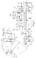
- FIG. 1is a partial front view of an exemplary embodiment of a wafer probe station constructed in accordance with the present invention.
- FIG. 2is a top view of the wafer probe station of FIG. 1 .
- FIG. 2Ais a partial top view of the wafer probe station of FIG. 1 with the enclosure door shown partially open.
- FIG. 3is a partially sectional and partially schematic front view of the probe station of FIG. 1 .
- FIG. 3Ais an enlarged sectional view taken along line 3 A— 3 A of FIG. 3 .
- FIG. 4is a top view of the sealing assembly where the motorized positioning mechanism extends through the bottom of the enclosure.
- FIG. 5Ais an enlarged top detail view taken along line 5 A— 5 A of FIG. 1 .
- FIG. 5Bis an enlarged top sectional view taken along line 5 B— 5 B of FIG. 1 .
- FIG. 6is a partially schematic top detail view of the chuck assembly, taken along line 6 — 6 of FIG. 3 .
- FIG. 7is a partially sectional front view of the chuck assembly of FIG. 6 .
- FIG. 8illustrates a probe station with a chuck that includes a stage with lift pins that is movable without x, y, and z positioners.
- FIG. 9illustrates a chuck with lift pins having a handle at zero degrees.
- FIG. 10illustrates a chuck with lift pins having a handle at six degrees.
- FIG. 11illustrates a chuck with lift pins having a handle at 12 degrees.
- FIG. 12illustrates a chuck with lift pins having a handle at 30 degrees.
- FIG. 13illustrates a side view of the chuck with the lift pins retracted.
- FIG. 14illustrates a side view of the chuck prior to lifting the lift pins.
- FIG. 15illustrates a side view of the chuck with the lift pins raised.
- FIG. 16illustrates a platen insert with even airflow.
- FIG. 17illustrates an air port
- FIG. 18illustrates a baffle around the chuck.
- the present inventorsconsidered existing roll out chuck stages and determined that it is easier to properly position a wafer on the rolled out chuck, together with the desired theta orientation of the wafer with respect to the chuck, when the chuck stage is extended at least partially outside of the chamber.
- the chuckis heated or cooled, such as to 300 degrees Celsius or cooled significantly below ambient temperature
- placing an ambient temperature wafer on the chucktends to result in damage to the devices on the wafer or otherwise results in fracturing the wafer itself.
- the waferis susceptible to becoming damaged.
- the usercould manually hold the wafer on a wafer holder in the vicinity of the chuck until the wafer is sufficiently heated, but this is difficult at best, for the user to accomplish.
- a roll-outincludes a stage that is movable with respect to the chamber.
- the stageat least partially exists the chamber while the x, y, z positioner remains within the chamber.
- a set of movable pins 200generally referred to as lift pins, incorporated within the roll-out chuck 210 would, (1) simplify the positioning of the wafer on the chuck by placing the wafer on the lift pins 200 , (2) decrease the likelihood of damage to the user's hand by accidently touching the chuck surface 212 , (3) permit the wafer to be held in a position above the chuck so that the wafer may adjust to a temperature closer to the temperature of the chuck surface, and/or (4) decrease the likelihood of the wafer sliding out of position.
- the lift pins 200 incorporated within the chuck 210may include a plurality of members spatially arranged around the chuck 210 that may be selectively raised and/or lowered. Alternatively, the lift pins may remain stationary and the surface of the chuck may be raised or lowered. In any case, the lift pins 200 and upper surface 212 of the chuck 210 include relative vertical motion with respect to one another. The maximum distance between the top of the lift pins and the upper surface of the chuck is preferably approximately 0.25 inches.
- a mechanical linkage systemincludes a handle 250 connected to a lever 252 that rotates about pivot point 254 (0 degrees of rotation) that may be rotated as illustrated in FIG. 10 (6 degrees of rotation), FIG. 11 (12 degrees of rotation), and FIG.
- the waferis properly positioned on the lift pins 200 .
- the wafermay be slowly heated or cooled by being spaced apart from the upper surface of the chuck, which decreases the likelihood of damaging the devices on the wafer or otherwise fracturing the wafer itself.
- the chuck 210 and the associated stageis locked out from being retracted within the chamber or otherwise being moved to a suitable probing position.
- the lift pinsare considered fully retracted when the lift pins are lowered to a level substantially even with the upper surface of the chuck or lower. In many cases, when the lift pins are extended the wafer is at a higher elevation than when the lift pins are retracted.
- a plate 256when fully retracted (see FIG. 12 ) inhibits a vacuum from a vacuum switch 260 from being provided to openings 216 in the upper surface 212 of the chuck 210 (hoses not shown).
- the plate 256is partially inserted within the vacuum switch 260 (see FIG. 11 ) as a result of rotating the lever 252 it causes a vacuum to be provided to the openings in the upper surface of the chuck.
- the lift pins 200are preferably partially retracted. Accordingly, the partial retraction of the lift pins 200 , and thus the lowering of the wafer toward the upper surface of the chuck, results in the activation of the vacuum switch 260 .
- the chuckmay be retracted within the chamber with the wafer supported thereon for subsequent probing. While the chuck is retracted within the chamber, or otherwise not fully extended, the handle is locked out from being moved.
- the locking out of the handle and thus the lift pin mechanismreduces the likelihood that the handle will be inadvertently moved or otherwise the lift pins will be in pressing engagement with the wafer that is being secured by the vacuum on the upper surface of the chuck. Otherwise there would be a possibility for the user to inadvertently move the handle and thus drive the lift pins through the wafer itself, thus damaging part of the wafer.
- the lockout of the lift pin mechanismis engaged when the chuck is sufficiently retracted or otherwise not fully extended, such as within the chamber. Also, the lockout of the lift pen mechanism is disengaged when the chuck is fully extended, or is otherwise at some point other than being fully retracted within the chamber for probing. Having the lockout mechanism engaged when the chuck is fully retracted reduces the likelihood of the user accidently causing the lift pins into pressing engagement with the wafer.
- having the lockout mechanism engaged when the chuck is fully retractedreduces the likelihood of lifting the wafer off the upper surface of the chuck into the probes, and the reduces the likelihood of the chuck being in motion while the wafer is supported by the lift pins thus causing the wafer to slide off the lift pins within the chamber if the chuck is abruptly moved.
- the lockout mechanism of the lift pinsis disengaged.
- the handle 250may be moved to lift the lift pins 200 .
- the motion of the handle 250moves a locking mechanism 258 , which causes the stage to be locked in position, as illustrated in FIG. 10 .
- the additional air pressureis preferably provided through the vacuum lines to the chuck, but may be provided using different openings.
- the air pressuremay be provided by the vacuum source.
- the air pressureis provided by expended air from a cylinder 272 that is used to raise and lower the lift pins through line 264 , where the air pressure results from the movement of the lever 252 .
- the motion of the handle 250 and lever 252causes the air pressure which helps to release the wafer from the upper surface of the chuck. Therefore, the air pressure will be provided to the upper surface of the chuck at the appropriate time and is not dependent upon whether the user moves the lever 252 quickly or slowly.
- One or more of the lockout features, and vacuum featuresmay be omitted or otherwise performed in a different order.
- the movement of the handle 250results in the shutting off the vacuum pressure to the wafer prior to raising the lift pins 200 above the upper surface of the chuck.
- the movement of the lever 252moves a pin 270 inwardly which results in the movement of the outer portion of the air cylinder 272 .
- the movement of the cylinder 272causes a decrease in the region between a piston 278 and the end of the cylinder 272 .
- the piston 278as a result of the increase in air pressure within the cylinder tends to move the drive plate 280 outwardly.
- the drive plate 280is connected to a lift plate 282 by a resilient mechanism, namely a spring 284 .
- a resilient mechanismnamely a spring 284 .
- the lift plate 282is likewise moved by the force applied by the spring 284 . Movement of the lift plate 282 results in a bearing 286 of a lift pin assembly 284 being raised as the bearing 286 moves up a ramp 288 .
- the lift pin assembly 284reduces its movement or otherwise is inhibited from movement by the resiliency of the spring 284 . It is noted that during the movement of the cylinder 272 air is routed through air line 264 to provide air to the upper surface of the chuck to reduce residual vacuum.
- This linkage systemprovides some added benefits.
- One such benefit of the linage systemis that the lift pin assembly 284 is not directly coupled to the lever 252 so that the applied force will not cause the lift pins 200 to break through the wafer.
- Another benefit of the linkage systemis to provide a elastic mechanism that inhibits the ability of the lift pins 200 to break through the wafer.
- Yet another benefit of the linkage systemis to inhibit the speed at which the lift pin assembly 284 may lift the lift pins by the action of the spring 284 . Accordingly, the speed at which the lift pins are raised is not a direct relationship to the speed at which the lever 252 is moved.
- the pressure exerted by the springwill tend to propel the lift plate assembly 282 upwardly, thus raising the wafer on the lift pins 200 .
- the piston 278moves in the cylinder 272 pulling in air.
- the chuck valve assemblyroutes air from the cylinder to the vacuum valve on the inward motion of the piston and provides makeup air via a needle valve as the piston pulls out. This controls the speed the pins lift once the suction is broken between the wafer and the chuck.
- the springpulls the lift plate until its stop is against the drive plate.
- the chuckpreferably extends the portion supporting the wafer, while the stage which provides x, y, and z movements is not extended.
- a set of one or more external pins or other membermay extend upwardly above the upper surface of the chuck from the region surrounding a part of the upper surface of the chuck.
- the external pinsinhibit the wafer from inadvertently sliding off the chuck.
- the external pinsextend above the height of the lift pins 200 when extended.
- the external pinspreferably are raised prior to raising the lift pins and are preferably lowered after lowering the lift pins. In this manner, the external pins inhibit the possibility of the wafer from sliding off the lift pins or otherwise sliding off the upper surface of the chuck.
- the lift pinsmay be electrically interconnected to the same potential as the upper surface of the chuck.
- the lift pinsmay be electrically interconnected to the shield potential, the guard potential, the ground potential, or a floating potential.
- the lift pinsmay also include holes therein to which is selectively provided vacuum so that the wafer is more securely secured to the lift pins. The vacuum may be provided or released between any of the functions of the lift pin assembly.
- the temperature of the chuck in thermal systemstends to vary between approximately ⁇ 65 degrees Celsius and 300 degrees Celsius.
- the chambershould (1) maintain the dew point of the air in the chamber below any surface temperature the air can contact; (2) introduce low velocity air across the probes, so as to avoid creating undesirable vibrations which could result in electrical noise; (3) transfer only a small amount of heat at the surface of the chuck to avoid the creation of significant temperature variations; (4) provide air to the chamber in a uniform manner to avoid non-uniform temperature variations; (5) limited heat transfer from the chuck to the air to facilitate rapid transition times between different measurements at different temperatures; and/or (6) transfer a small amount of heat at the walls of the microchamber, so as to avoid “sweating” of the outside of the microchamber under cold conditions, and to avoid creating a burning hazard under hot conditions.
- the chamberpreferably includes one or more inlets for air, such as through the top hat and/or inlets to the chamber, and includes one or more defined outlets for the air, such as through the top hat and/or inlets to the chamber.
- the chamberincludes a series of leakage paths to facilitate the exit of air.
- the systempreferably includes in excess of 75%, more preferably 90%, of the air exiting the chamber to pass through the defined outlets. In this manner, the flow of air through the chamber may be more accurately controlled. In this manner, minor differences in the construction of one probe station to another probe station will have negligible impact on the resulting air flow.
- the preferred air entry into the chamberincludes a plurality of spaced apart ports.
- the air entry pointsinclude one above the chuck itself, such as within the top hat, and a port proximate to each of the upper corners of the chamber.
- the principal designated air exitis preferably in the central region of the side wall of the chamber, having a size of approximately 1.5 inches by 4.5 inches.
- the air entry above the chuckis specifically designed to introduce the air through a platen insert in a low velocity, substantially laminar flow, having a radial component of velocity.
- the insertmay include a pair of plates and baffles that substantially distribute air evenly around the platen insert.
- the airmay enter through three, four, five, six, or more openings. The intention is to provide the air drop smoothly through the opening in the platen onto the chuck where it smoothly distributes radially outward over the chuck.
- Another function of the air introductioninvolves air leakage through the top hat of the probe station. Under cold operating conditions, the chuck should produce a mild pumping action from the cold, heavier air flowing off the edges of the chuck.
- a more suitable port to the chamberincludes a diffuser that includes a plate of porous sintered stainless steel (such as 5 micron pore size) sandwiched in a frame.
- the air pressureis preferably connected to the base (shown on the right) and passes into a plenum behind the porous plate before being substantially evenly distributed by passing through it.
- the air exit from the chambermay include a purge vent.
- the ventmay include a plurality of identical, convoluted air passages that are stacked upon one another.
- the purpose of the air passageis to provide a low pressure drop laminar airflow path that would attenuate the passage of light and low frequency electromagnetic waves. In this manner there is no straight path through the air exit from the interior to the exterior of the chamber.
- a chambermay include air introduction above the wafer with a substantially sealed chamber together with controlled exhaust.
- the air introduced onto the wafer from the top hatworks well when the chuck is generally centered under the opening in the platen.
- the air flowwill be sufficiently uneven because a portion of the air will not impact the chuck, but rather, will pass straight down (or with minor deviation) into the chamber.
- a baffle membermay be included around at least a portion of the chuck, and more preferably around the majority, 75%, 95%, or 100% of the periphery of the chuck.
- the baffle membertends to act as an extension of the chuck and preferably has a sufficient width so that if the chuck is being probed at any particular edge, the baffle is still under all of the opening provided by the platen.
- the width of the bafflemay be the same as the opening in the platen.
Landscapes
- Engineering & Computer Science (AREA)
- Computer Hardware Design (AREA)
- Microelectronics & Electronic Packaging (AREA)
- General Engineering & Computer Science (AREA)
- Physics & Mathematics (AREA)
- General Physics & Mathematics (AREA)
- Testing Or Measuring Of Semiconductors Or The Like (AREA)
- Container, Conveyance, Adherence, Positioning, Of Wafer (AREA)
Abstract
Description
This application claims the benefit of U.S. patent application Ser. No. 60/532,757, filed Dec. 24, 2003.
The present application relates to an improved chuck and an improved probe station.
With reference toFIGS. 1 ,2 and3, a probe station comprises a base10 (shown partially) which supports aplaten 12 through a number ofjacks base 10 of the probe station is amotorized positioner 16 having arectangular plunger 18 which supports amovable chuck assembly 20 for supporting a wafer or other test device. Thechuck assembly 20 passes freely through alarge aperture 22 in theplaten 12 which permits the chuck assembly to be moved independently of the platen by thepositioner 16 along X, Y and Z axes, i.e. horizontally along two mutually-perpendicular axes X and Y, and vertically along the Z axis. Likewise, theplaten 12, when moved vertically by the jacks14, moves independently of thechuck assembly 20 and thepositioner 16.
Mounted atop theplaten 12 are multiple individual probe positioners such as24 (only one of which is shown), each having an extendingmember 26 to which is mounted aprobe holder 28 which in turn supports arespective probe 30 for contacting wafers and other test devices mounted atop thechuck assembly 20. Theprobe positioner 24 hasmicrometer adjustments probe holder 28, and thus theprobe 30, along the X, Y and Z axes respectively, relative to thechuck assembly 20. The Z axis is exemplary of what is referred to herein loosely as the “axis of approach” between theprobe holder 28 and thechuck assembly 20, although directions of approach which are neither vertical nor linear, along which the probe tip and wafer or other test device are brought into contact with each other, are also intended to be included within the meaning of the term “axis of approach.” Afurther micrometer adjustment 40 adjustably tilts theprobe holder 28 to adjust planarity of the probe with respect to the wafer or other test device supported by thechuck assembly 20. As many as twelveindividual probe positioners 24, each supporting a respective probe, may be arranged on theplaten 12 around thechuck assembly 20 so as to converge radially toward the chuck assembly similarly to the spokes of a wheel. With such an arrangement, eachindividual positioner 24 can independently adjust its respective probe in the X, Y and Z directions, while the jacks14 can be actuated to raise or lower theplaten 12 and thus all of thepositioners 24 and their respective probes in unison.
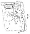
An environment control enclosure is composed of anupper box portion 42 rigidly attached to theplaten 12, and alower box portion 44 rigidly attached to thebase 10. Both portions are made of steel or other suitable electrically conductive material to provide EMI shielding. To accommodate the small vertical movement between the twobox portions platen 12, an electrically conductiveresilient foam gasket 46, preferably composed of silver or carbon-impregnated silicone, is interposed peripherally at their mating juncture at the front of the enclosure and between thelower portion 44 and theplaten 12 so that an EMI, substantially hermetic, and light seal are all maintained despite relative vertical movement between the twobox portions upper box portion 42 is rigidly attached to theplaten 12, asimilar gasket 47 is preferably interposed between theportion 42 and the top of the platen to maximize sealing.
With reference toFIGS. 5A and 5B , the top of theupper box portion 42 comprises anoctagonal steel box 48 having eight side panels such as49aand49bthrough which the extendingmembers 26 of therespective probe positioners 24 can penetrate movably. Each panel comprises a hollow housing in which arespective sheet 50 of resilient foam, which may be similar to the above-identified gasket material, is placed. Slits such as52 are partially cut vertically in the foam in alignment withslots 54 formed in the inner and outer surfaces of each panel housing, through which a respective extendingmember 26 of arespective probe positioner 24 can pass movably. The slitted foam permits X, Y and Z movement of the extendingmembers 26 of each probe positioner, while maintaining the EMI, substantially hermetic, and light seal provided by the enclosure. In four of the panels, to enable a greater range of X and Y movement, thefoam sheet 50 is sandwiched between a pair ofsteel plates 55 havingslots 54 therein, such plates being slidable transversely within the panel housing through a range of movement encompassed bylarger slots 56 in the inner and outer surfaces of the panel housing.
Atop theoctagonal box 48, acircular viewing aperture 58 is provided, having a recessed circulartransparent sealing window 60 therein. Abracket 62 holds an apertured slidingshutter 64 to selectively permit or prevent the passage of light through the window. A stereoscope (not shown) connected to a CRT monitor can be placed above the window to provide a magnified display of the wafer or other test device and the probe tip for proper probe placement during set-up or operation. Alternatively, thewindow 60 can be removed and a microscope lens (not shown) surrounded by a foam gasket can be inserted through theviewing aperture 58 with the foam providing EMI, hermetic and light sealing. Theupper box portion 42 of the environment control enclosure also includes a hingedsteel door 68 which pivots outwardly about the pivot axis of ahinge 70 as shown inFIG. 2A . The hinge biases the door downwardly toward the top of theupper box portion 42 so that it forms a tight, overlapping, slidingperipheral seal 68awith the top of the upper box portion. When the door is open, and thechuck assembly 20 is moved by thepositioner 16 beneath the door opening as shown inFIG. 2A , the chuck assembly is accessible for loading and unloading.
With reference toFIGS. 3 and 4 , the sealing integrity of the enclosure is likewise maintained throughout positioning movements by themotorized positioner 16 due to the provision of a series of foursealing plates central apertures respective plates aperture 79aformed in thebottom 44aof thelower box portion 44. Thecentral aperture 72ain thetop plate 72 mates closely around thebearing housing 18aof the vertically-movable plunger 18. The next plate in the downward progression,plate 74, has an upwardly-projectingperipheral margin 74bwhich limits the extent to which theplate 72 can slide across the top of theplate 74. Thecentral aperture 74ain theplate 74 is of a size to permit thepositioner 16 to move theplunger 18 and its bearing housing18 a transversely along the X and Y axes until the edge of thetop plate 72 abuts against themargin 74bof theplate 74. The size of theaperture 74ais, however, too small to be uncovered by thetop plate 72 when such abutment occurs, and therefore a seal is maintained between theplates plunger 18 and its bearing housing along the X and Y axes. Further movement of theplunger 18 and bearing housing in the direction of abutment of theplate 72 with themargin 74bresults in the sliding of theplate 74 toward theperipheral margin 76bof the nextunderlying plate 76. Again, thecentral aperture 76ain theplate 76 is large enough to permit abutment of theplate 74 with themargin 76b, but small enough to prevent theplate 74 from uncovering theaperture 76a, thereby likewise maintaining the seal between theplates plunger 18 and bearing housing in the same direction causes similar sliding of theplates margin 78band the side of thebox portion 44, respectively, without theapertures plunger 18 along the X and Y axes by thepositioner 16, while maintaining the enclosure in a sealed condition despite such positioning movement. The EMI sealing provided by this structure is effective even with respect to the electric motors of thepositioner 16, since they are located below the sliding plates.
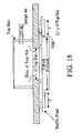
With particular reference toFIGS. 3 ,6 and7, thechuck assembly 20 is a modular construction usable either with or without an environment control enclosure. Theplunger 18 supports anadjustment plate 79 which in turn supports first, second and thirdchuck assembly elements Element 83 is a conductive rectangular stage orshield 83 which detachably mountsconductive elements element 80 has a planar upwardly-facing wafer-supportingsurface 82 having an array ofvertical apertures 84 therein. These apertures communicate with respective chambers separated by O-rings 88, the chambers in turn being connected separately todifferent vacuum lines FIG. 6 ) communicating through separately-controlled vacuum valves (not shown) with a source of vacuum. The respective vacuum lines selectively connect the respective chambers and their apertures to the source of vacuum to hold the wafer, or alternatively isolate the apertures from the source of vacuum to release the wafer, in a conventional manner. The separate operability of the respective chambers and their corresponding apertures enables the chuck to hold wafers of different diameters.
In addition to thecircular elements element 83 by screws (not shown) independently of theelements element 80. Eachauxiliary chuck planar surface surface 82 of theelement 80.Vacuum apertures 104 protrude through thesurfaces apertures 104 with respect to the source of vacuum independently of the operation of theapertures 84 of theelement 80, so as to selectively hold or release a contact substrate or calibration substrate located on therespective surfaces optional metal shield 106 may protrude upwardly from the edges of theelement 83 to surround theother elements auxiliary chucks
All of thechuck assembly elements chuck assembly element 79, are electrically insulated from one another even though they are constructed of electrically conductive metal and interconnected detachably by metallic screws such as96. With reference toFIGS. 3 and 3A , the electrical insulation results from the fact that, in addition to the resilient dielectric O-rings 88,dielectric spacers 85 anddielectric washers 86 are provided. These, coupled with the fact that thescrews 96 pass through oversized apertures in the lower one of the two elements which each screw joins together thereby preventing electrical contact between the shank of the screw and the lower element, provide the desired insulation. As is apparent inFIG. 3 , thedielectric spacers 85 extend over only minor portions of the opposing surface areas of the interconnected chuck assembly elements, thereby leaving air gaps between the opposing surfaces over major portions of their respective areas. Such air gaps minimize the dielectric constant in the spaces between the respective chuck assembly elements, thereby correspondingly minimizing the capacitance between them and the ability for electrical current to leak from one element to another. Preferably the spacers andwashers
With reference toFIGS. 6 and 7 , thechuck assembly 20 also includes a pair of detachable electrical connector assemblies designated generally as108 and110, each having at least twoconductive connector elements connector elements connector elements connector assemblies outer shields respective connector elements FIG. 7 . Theouter shields shielding box 112 and aconnector supporting bracket 113 to thechuck assembly element 83, although such electrical connection is optional particularly in view of the surroundingEMI shielding enclosure respective connector elements connector plate 114 matingly and detachably connected along acurved contact surface 114abyscrews chuck assembly element 80. Conversely, theconnector elements connector plate 116 similarly matingly connected detachably toelement 81. The connector elements pass freely through arectangular opening 112ain thebox 112, being electrically insulated from thebox 112 and therefore from theelement 83, as well as being electrically insulated from each other. Set screws such as118 detachably fasten the connector elements to therespective connector plates
Either coaxial or, as shown,triaxial cables electrical connector assemblies detachable connectors lower portion 44 of the environment control enclosure so that the outer shields of thetriaxial connectors triaxial cables 122a,124aare detachably connectable to theconnectors cables respective connector respective connector element respective connector respective connector element
Thechuck assembly 20 with correspondingvertical apertures 84 and respective chambers separated by O-rings 88 permits selectively creating a vacuum within three different zones. Including the three O-rings 88 and thedielectric spacers 85 surrounding themetallic screws 96 permits securing adjacent first, second and thirdchuck assembly elements rings 88 are squeezed by the first and second chuck assembly elements and assist in distributing the force across the upper surface of thechuck assembly 20 to maintain a flat surface. However, the O-rings anddielectric spacers 85 have a greater dielectric constant than the surrounding air resulting in leakage currents. Also, the additional material between adjoiningchuck assembly elements dielectric spacers 85 builds up a charge therein during testing which increases the dielectric absorption. The O-rings anddielectric spacers 85 provides mechanical stability against warping the chuck when a wafer thereon is probed so that thinnerchuck assembly elements dielectric spacers 85 tend to be slightly different which introduces non-planarity in the upper surface when the first, second, and thirdchuck assembly elements
The present inventors considered existing roll out chuck stages and determined that it is easier to properly position a wafer on the rolled out chuck, together with the desired theta orientation of the wafer with respect to the chuck, when the chuck stage is extended at least partially outside of the chamber. Unfortunately, in the event that the chuck is heated or cooled, such as to 300 degrees Celsius or cooled significantly below ambient temperature, placing an ambient temperature wafer on the chuck tends to result in damage to the devices on the wafer or otherwise results in fracturing the wafer itself. In either case, the wafer is susceptible to becoming damaged. In some cases the user could manually hold the wafer on a wafer holder in the vicinity of the chuck until the wafer is sufficiently heated, but this is difficult at best, for the user to accomplish. Further, it is difficult to achieve similar such temperatures using a wafer holder because of the insulating effect of the wafer holder and the distance of the wafer from the surface of the chuck. Also, the user has a tendency to accidently touch the surface of the chuck with his hand, thus resulting in painful burning or freezing of his hand. In addition, even with a chuck at ambient temperature the wafer is typically placed on the upper surface of the chuck using a motion that is at an acute angle to the upper surface of the chuck, and accordingly, the wafer tends to slide across the chuck surface thus coming to rest at a non-desirable location, if it remains on the chuck at all.
Referring toFIG. 8 , a roll-out includes a stage that is movable with respect to the chamber. Preferably, the stage at least partially exists the chamber while the x, y, z positioner remains within the chamber. To alleviate concerns the present inventors came to the realization that a set ofmovable pins 200, generally referred to as lift pins, incorporated within the roll-out chuck 210 would, (1) simplify the positioning of the wafer on the chuck by placing the wafer on the lift pins200, (2) decrease the likelihood of damage to the user's hand by accidently touching thechuck surface 212, (3) permit the wafer to be held in a position above the chuck so that the wafer may adjust to a temperature closer to the temperature of the chuck surface, and/or (4) decrease the likelihood of the wafer sliding out of position. The lift pins200 incorporated within thechuck 210 may include a plurality of members spatially arranged around thechuck 210 that may be selectively raised and/or lowered. Alternatively, the lift pins may remain stationary and the surface of the chuck may be raised or lowered. In any case, the lift pins200 andupper surface 212 of thechuck 210 include relative vertical motion with respect to one another. The maximum distance between the top of the lift pins and the upper surface of the chuck is preferably approximately 0.25 inches.
One technique to engage the lift pins is to use a motor, such as a stepper motor, to lift the pins. The stepper motor may be controlled by software or otherwise by the user indicating the desire to lift or lower the lift pins. Another alternative to engage the lift pins is to use a pneumatic system that is controlled by software or otherwise by the user indicating the desire to lift or lower the lift pins. Another technique, that provides more tactile feedback to the user is to use a mechanical linkage system controlled by the user. Referring toFIG. 9 , a mechanical linkage system includes ahandle 250 connected to alever 252 that rotates about pivot point254 (0 degrees of rotation) that may be rotated as illustrated inFIG. 10 (6 degrees of rotation),FIG. 11 (12 degrees of rotation), andFIG. 12 (30 degrees of rotation) to fully extend the lift pins200 above the upper surface of the chuck. With the lift pins200 extended, as illustrated inFIG. 12 , the wafer is properly positioned on the lift pins200. In addition, in the event that the upper surface of the chuck is not at ambient temperature, the user is not likely to accidently touch the chuck. Also, the wafer may be slowly heated or cooled by being spaced apart from the upper surface of the chuck, which decreases the likelihood of damaging the devices on the wafer or otherwise fracturing the wafer itself.
When the lift pins are fully extended or otherwise are not fully retracted, thechuck 210 and the associated stage is locked out from being retracted within the chamber or otherwise being moved to a suitable probing position. The lift pins are considered fully retracted when the lift pins are lowered to a level substantially even with the upper surface of the chuck or lower. In many cases, when the lift pins are extended the wafer is at a higher elevation than when the lift pins are retracted. By inhibiting the stage from being retracted within the chamber when the lift pins are not fully retracted, or otherwise the lift pins are fully extended, reduces the likelihood that the wafer will inadvertently strike a probe upon retraction of the stage within the chamber.
Moving the handle of the lift mechanism from 30 degrees as illustrated inFIG. 12 , to 12 degrees as illustrated inFIG. 11 , rotates thelever 252 about thepivot point 254. Aplate 256 when fully retracted (seeFIG. 12 ) inhibits a vacuum from avacuum switch 260 from being provided toopenings 216 in theupper surface 212 of the chuck210 (hoses not shown). When theplate 256 is partially inserted within the vacuum switch260 (seeFIG. 11 ) as a result of rotating thelever 252 it causes a vacuum to be provided to the openings in the upper surface of the chuck. In addition, while moving thelever 252 the lift pins200 are preferably partially retracted. Accordingly, the partial retraction of the lift pins200, and thus the lowering of the wafer toward the upper surface of the chuck, results in the activation of thevacuum switch 260.
Further retraction of the lift pins200 by rotating thehandle 250 of the lever to six degrees, as illustrated inFIG. 10 , results in the disengagement of the roll out interlock258 (locking mechanism). In this manner, the wafer is close to the upper surface of the chuck and is less likely to impact the probes if moved within the chamber. The lockout of the chuck may also be released when the lift pins are fully retracted or otherwise the wafer is supported by the upper surface of the chuck. Also, the release of the lockout mechanism while the lift pins200 maintain the wafer above the upper surface of the chuck permits the chuck to be retracted within the chamber so that the wafer and upper surface of the chuck may both substantially reach the desired operating temperature.
Further retraction of the lift pins by rotating the handle of the lift mechanism to 0 degrees, as illustrated inFIG. 9 , results in the wafer being supported by the upper surface of the chuck. The lift pins are typically recessed slightly below the upper surface of the chuck or otherwise substantially even with the upper surface of the chuck. Engaging the vacuum source prior to, or simultaneously therewith, the wafer coming into contact with the upper surface of the chuck reduces the likelihood that the wafer will skate or otherwise exhibit undesirable movement on the upper surface of the chuck.
The chuck may be retracted within the chamber with the wafer supported thereon for subsequent probing. While the chuck is retracted within the chamber, or otherwise not fully extended, the handle is locked out from being moved. The locking out of the handle and thus the lift pin mechanism reduces the likelihood that the handle will be inadvertently moved or otherwise the lift pins will be in pressing engagement with the wafer that is being secured by the vacuum on the upper surface of the chuck. Otherwise there would be a possibility for the user to inadvertently move the handle and thus drive the lift pins through the wafer itself, thus damaging part of the wafer.
The lockout of the lift pin mechanism is engaged when the chuck is sufficiently retracted or otherwise not fully extended, such as within the chamber. Also, the lockout of the lift pen mechanism is disengaged when the chuck is fully extended, or is otherwise at some point other than being fully retracted within the chamber for probing. Having the lockout mechanism engaged when the chuck is fully retracted reduces the likelihood of the user accidently causing the lift pins into pressing engagement with the wafer. Also, having the lockout mechanism engaged when the chuck is fully retracted reduces the likelihood of lifting the wafer off the upper surface of the chuck into the probes, and the reduces the likelihood of the chuck being in motion while the wafer is supported by the lift pins thus causing the wafer to slide off the lift pins within the chamber if the chuck is abruptly moved.
When the chuck is fully extended or otherwise sufficiently moved from its probing position, the lockout mechanism of the lift pins is disengaged. Referring again toFIG. 9 , thehandle 250 may be moved to lift the lift pins200. The motion of thehandle 250 moves alocking mechanism 258, which causes the stage to be locked in position, as illustrated inFIG. 10 .
Sufficient rotation of thehandle 250 andlever 252 causes theplate 256 to be retracted fromvacuum switch 260 which turns off the vacuum to the upper surface of the chuck, as illustrated inFIG. 11 . The mechanical motion of thehandle 250 andlever 252 disengaging thevacuum switch 260 facilitates the wafer being lifted from the upper surface of the chuck. With the wafer securement mechanism being released, the wafer is more readily lifted by the lift pins200.
After disengaging the vacuum to the upper surface of the chuck it turns out that there remains a residual vacuum suction between the upper surface of the chuck and the wafer which impedes lifting the wafer. To release the residual vacuum suction it was determined that a limited amount of air should be provided to the lower surface of the wafer. The additional air pressure is preferably provided through the vacuum lines to the chuck, but may be provided using different openings. The air pressure may be provided by the vacuum source. Preferably the air pressure is provided by expended air from acylinder 272 that is used to raise and lower the lift pins throughline 264, where the air pressure results from the movement of thelever 252. In this manner, the motion of thehandle 250 andlever 252 causes the air pressure which helps to release the wafer from the upper surface of the chuck. Therefore, the air pressure will be provided to the upper surface of the chuck at the appropriate time and is not dependent upon whether the user moves thelever 252 quickly or slowly. One or more of the lockout features, and vacuum features may be omitted or otherwise performed in a different order.
As previously noted, the movement of thehandle 250 results in the shutting off the vacuum pressure to the wafer prior to raising the lift pins200 above the upper surface of the chuck. As illustrated in FIGS.9—12, the movement of thelever 252 moves apin 270 inwardly which results in the movement of the outer portion of theair cylinder 272. Referring toFIG. 13 (lever at 0 degrees), the movement of thecylinder 272 causes a decrease in the region between apiston 278 and the end of thecylinder 272. Referring toFIG. 14 , thepiston 278 as a result of the increase in air pressure within the cylinder tends to move thedrive plate 280 outwardly. Thedrive plate 280 is connected to alift plate 282 by a resilient mechanism, namely aspring 284. As thedrive plate 280 is moved, thelift plate 282 is likewise moved by the force applied by thespring 284. Movement of thelift plate 282 results in abearing 286 of alift pin assembly 284 being raised as the bearing286 moves up aramp 288. As it may be observed, if the wafer is stuck to the upper surface of the chuck by residual vacuum, thelift pin assembly 284 reduces its movement or otherwise is inhibited from movement by the resiliency of thespring 284. It is noted that during the movement of thecylinder 272 air is routed throughair line 264 to provide air to the upper surface of the chuck to reduce residual vacuum. This linkage system provides some added benefits. One such benefit of the linage system is that thelift pin assembly 284 is not directly coupled to thelever 252 so that the applied force will not cause the lift pins200 to break through the wafer. Another benefit of the linkage system is to provide a elastic mechanism that inhibits the ability of the lift pins200 to break through the wafer. Yet another benefit of the linkage system is to inhibit the speed at which thelift pin assembly 284 may lift the lift pins by the action of thespring 284. Accordingly, the speed at which the lift pins are raised is not a direct relationship to the speed at which thelever 252 is moved.
Referring toFIG. 15 , once the residual vacuum is relieved between the wafer and the upper surface of the chuck, the pressure exerted by the spring will tend to propel thelift plate assembly 282 upwardly, thus raising the wafer on the lift pins200. Since thedrive plate 280 is stationary when thelever 252 is fully rotated, thepiston 278 moves in thecylinder 272 pulling in air. The chuck valve assembly routes air from the cylinder to the vacuum valve on the inward motion of the piston and provides makeup air via a needle valve as the piston pulls out. This controls the speed the pins lift once the suction is broken between the wafer and the chuck. The spring pulls the lift plate until its stop is against the drive plate.
It may be observed that the chuck preferably extends the portion supporting the wafer, while the stage which provides x, y, and z movements is not extended. In one embodiment, a set of one or more external pins or other member may extend upwardly above the upper surface of the chuck from the region surrounding a part of the upper surface of the chuck. The external pins inhibit the wafer from inadvertently sliding off the chuck. Preferably, the external pins extend above the height of the lift pins200 when extended. In addition, the external pins preferably are raised prior to raising the lift pins and are preferably lowered after lowering the lift pins. In this manner, the external pins inhibit the possibility of the wafer from sliding off the lift pins or otherwise sliding off the upper surface of the chuck.
In some embodiments, the lift pins may be electrically interconnected to the same potential as the upper surface of the chuck. Alternatively, the lift pins may be electrically interconnected to the shield potential, the guard potential, the ground potential, or a floating potential. The lift pins may also include holes therein to which is selectively provided vacuum so that the wafer is more securely secured to the lift pins. The vacuum may be provided or released between any of the functions of the lift pin assembly.
The temperature of the chuck in thermal systems tends to vary between approximately −65 degrees Celsius and 300 degrees Celsius. When the thermal system undergoes cold conditions it is possible for ice crystals to form on the wafer under test. To inhibit the creation of ice crystals the chamber should (1) maintain the dew point of the air in the chamber below any surface temperature the air can contact; (2) introduce low velocity air across the probes, so as to avoid creating undesirable vibrations which could result in electrical noise; (3) transfer only a small amount of heat at the surface of the chuck to avoid the creation of significant temperature variations; (4) provide air to the chamber in a uniform manner to avoid non-uniform temperature variations; (5) limited heat transfer from the chuck to the air to facilitate rapid transition times between different measurements at different temperatures; and/or (6) transfer a small amount of heat at the walls of the microchamber, so as to avoid “sweating” of the outside of the microchamber under cold conditions, and to avoid creating a burning hazard under hot conditions.
The chamber preferably includes one or more inlets for air, such as through the top hat and/or inlets to the chamber, and includes one or more defined outlets for the air, such as through the top hat and/or inlets to the chamber. Typically the chamber includes a series of leakage paths to facilitate the exit of air. The system preferably includes in excess of 75%, more preferably 90%, of the air exiting the chamber to pass through the defined outlets. In this manner, the flow of air through the chamber may be more accurately controlled. In this manner, minor differences in the construction of one probe station to another probe station will have negligible impact on the resulting air flow.
The preferred air entry into the chamber includes a plurality of spaced apart ports. The air entry points include one above the chuck itself, such as within the top hat, and a port proximate to each of the upper corners of the chamber. The principal designated air exit is preferably in the central region of the side wall of the chamber, having a size of approximately 1.5 inches by 4.5 inches.
Referring toFIG. 16 , the air entry above the chuck is specifically designed to introduce the air through a platen insert in a low velocity, substantially laminar flow, having a radial component of velocity. The insert may include a pair of plates and baffles that substantially distribute air evenly around the platen insert. For example, the air may enter through three, four, five, six, or more openings. The intention is to provide the air drop smoothly through the opening in the platen onto the chuck where it smoothly distributes radially outward over the chuck. Another function of the air introduction involves air leakage through the top hat of the probe station. Under cold operating conditions, the chuck should produce a mild pumping action from the cold, heavier air flowing off the edges of the chuck. This flow of air should produce a slight vacuum in the center of the chuck that would tend to suck air through the top hat. Introducing air above the chuck helps assure that the pressure inside the top hat is always positive with respect to the pressure outside it. It has been determined that air flow between 8 and 12 cfh (0.13 to 0.2 cfm) is sufficient to reduce air leakage from the top hat and to provide a radial flow across the chuck having a velocity of a few millimeters per second at the outer edge.
While simply an opening may be provided between the interior of the chamber and the exterior of the chamber, such an opening tends to be sub-optimal when making low current low noise measurements. Referring toFIG. 17 , a more suitable port to the chamber includes a diffuser that includes a plate of porous sintered stainless steel (such as 5 micron pore size) sandwiched in a frame. The air pressure is preferably connected to the base (shown on the right) and passes into a plenum behind the porous plate before being substantially evenly distributed by passing through it.
The air exit from the chamber may include a purge vent. The vent may include a plurality of identical, convoluted air passages that are stacked upon one another. The purpose of the air passage is to provide a low pressure drop laminar airflow path that would attenuate the passage of light and low frequency electromagnetic waves. In this manner there is no straight path through the air exit from the interior to the exterior of the chamber.
It may be observed that a chamber may include air introduction above the wafer with a substantially sealed chamber together with controlled exhaust. However, the air introduced onto the wafer from the top hat works well when the chuck is generally centered under the opening in the platen. However, when the chuck is sufficiently displaced to the side with respect to the opening for the top hat, then the air flow will be sufficiently uneven because a portion of the air will not impact the chuck, but rather, will pass straight down (or with minor deviation) into the chamber.
Referring toFIG. 18 , to even out the air flow across the chuck when the chuck is sufficiently laterally displaced with respect to the opening in the top hat a baffle member may be included around at least a portion of the chuck, and more preferably around the majority, 75%, 95%, or 100% of the periphery of the chuck. The baffle member tends to act as an extension of the chuck and preferably has a sufficient width so that if the chuck is being probed at any particular edge, the baffle is still under all of the opening provided by the platen. For example, the width of the baffle may be the same as the opening in the platen. Further, there may be an opening around a majority of the chuck between the chuck and the baffle plate to provide for electrical isolation and an opening for the air to flow over the edge of the chuck.
Claims (19)
1. A probe station comprising:
(a) a chamber that at least partially encloses a chuck assembly therein;
(b) said chuck assembly having an upper surface thereon suitable to support a wafer thereon;
(c) a plurality of members located within a periphery of said chuck assembly suitable to support said wafer on said plurality of members while said wafer is not simultaneously supported by said upper surface;
(d) said members and said upper surface capable of relative vertical movement with respect to one another such that said wafer may be moved between a position where said wafer is supported by said plurality of members while not simultaneously supported by said upper surface, and a position where said wafer is supported by said upper surface;
(e) said chuck assembly movable from a location completely within said chamber to a location at least partially outside said chamber.
2. The probe station ofclaim 1 wherein said chamber is substantially airtight.
3. The probe station ofclaim 1 wherein said chuck includes a thermal unit to raise the temperature of said upper surface above ambient temperature.
4. The probe station ofclaim 1 wherein said chuck includes a thermal unit to lower the temperature of said upper surface below ambient temperature.
5. The probe station ofclaim 1 wherein said upper surface is substantially flat.
6. The probe station ofclaim 1 wherein said plurality of members are substantially evenly spaced around said chuck.
7. The probe station ofclaim 1 wherein said plurality of members are selectively raised or lowered.
8. The probe station ofclaim 1 wherein said plurality of members are capable of being maintained at different elevations above said upper surface.
9. The probe station ofclaim 1 wherein said plurality of members are movable in response to movement of a handle by a user.
10. A chuck assembly comprising:
(a) said chuck assembly having an upper surface thereon suitable to support a wafer thereon;
(b) a plurality of members located within the periphery of said chuck assembly suitable to support said wafer on said plurality of members while said wafer is not simultaneously supported by said upper surface;
(c) said members and said upper surface capable of relative vertical movement with respect to one another such that said wafer may be moved between a position where said wafer is supported by said plurality of members while not simultaneously supported by said upper surface, and a position where said wafer is supported by said upper surface;
(d) said chuck assembly inhibited from lateral movement when said plurality of members are fully extended.
11. The chuck ofclaim 10 wherein said lateral movement is not inhibited when said plurality of members are fully retracted.
12. The chuck ofclaim 10 wherein said lateral movement is not inhibited when said plurality of members are not fully extended.
13. The chuck ofclaim 10 wherein vacuum is supplied to said upper surface of said chuck while said members are being retracted.
14. The chuck ofclaim 10 wherein vacuum is supplied to said upper surface of said chuck while said members are free from being extended above the upper surface of said chuck and said vacuum is reduced prior to extending said members above said upper surface of said chuck as a result of a user lifting said lift pins.
15. A chuck assembly comprising:
(a) said chuck assembly having an upper surface thereon suitable to support a wafer thereon;
(b) a plurality of members located within the periphery of said chuck assembly suitable to support said wafer on said plurality of members while said wafer is not simultaneously supported by said upper surface;
(c) said members and said upper surface capable of relative vertical movement with respect to one another such that said wafer may be moved between a position where said wafer is supported by said plurality of members while not simultaneously supported by said upper surface, and a position where said wafer is supported by said upper surface;
(d) increasing a vacuum provided to said upper surface as a result of decreasing the extension of said plurality of members, where said plurality of members are not substantially even with said upper surface.
16. The chuck assembly ofclaim 15 wherein said decreasing said extension is from a point of full extension of said plurality of members to a point intermediate to said plurality of members being substantially even with said upper surface.
17. The chuck assembly ofclaim 15 wherein no vacuum is provided when said plurality of members are at said full extension.
18. A chuck assembly comprising:
(a) said chuck assembly having an upper surface thereon suitable to support a wafer thereon;
(b) a plurality of members located within the periphery of said chuck assembly suitable to support said wafer on said plurality of members while said wafer is not simultaneously supported by said upper surface;
(c) said members and said upper surface capable of relative vertical movement with respect to one another such that said wafer may be moved between a position where said wafer is supported by said plurality of members while not simultaneously supported by said upper surface, and a position where said wafer is supported by said upper surface;
(d) said chuck assembly inhibited from lateral movement when said plurality of members are at a first height above said upper surface and free from being inhibited when said plurality of members are at a second height above said upper surface, wherein said first height is greater than said second height.
19. A chuck assembly comprising:
(a) said chuck assembly having an upper surface thereon suitable to support a wafer thereon;
(b) a plurality of members located within the periphery of said chuck assembly suitable to support said wafer on said plurality of members while said wafer is not simultaneously supported by said upper surface;
(c) said members and said upper surface capable of relative vertical movement with respect to one another such that said wafer may be moved between a position where said wafer is supported by said plurality of members while not simultaneously supported by said upper surface, and a position where said wafer is supported by said upper surface;
(d) said chuck assembly inhibited from relative movement of said members to a position above said upper surface when said shuck assembly is in a position suitable for probing said wafer.
Priority Applications (4)
| Application Number | Priority Date | Filing Date | Title |
|---|---|---|---|
| US10/927,247US7187188B2 (en) | 2003-12-24 | 2004-08-26 | Chuck with integrated wafer support |
| PCT/US2004/030276WO2005067445A2 (en) | 2003-12-24 | 2004-09-14 | Chuck with integrated wafer support |
| US11/655,605US7362115B2 (en) | 2003-12-24 | 2007-01-19 | Chuck with integrated wafer support |
| US12/075,385US7688091B2 (en) | 2003-12-24 | 2008-03-10 | Chuck with integrated wafer support |
Applications Claiming Priority (2)
| Application Number | Priority Date | Filing Date | Title |
|---|---|---|---|
| US53275703P | 2003-12-24 | 2003-12-24 | |
| US10/927,247US7187188B2 (en) | 2003-12-24 | 2004-08-26 | Chuck with integrated wafer support |
Related Child Applications (1)
| Application Number | Title | Priority Date | Filing Date |
|---|---|---|---|
| US11/655,605ContinuationUS7362115B2 (en) | 2003-12-24 | 2007-01-19 | Chuck with integrated wafer support |
Publications (2)
| Publication Number | Publication Date |
|---|---|
| US20050140384A1 US20050140384A1 (en) | 2005-06-30 |
| US7187188B2true US7187188B2 (en) | 2007-03-06 |
Family
ID=34704332
Family Applications (3)
| Application Number | Title | Priority Date | Filing Date |
|---|---|---|---|
| US10/927,247Expired - Fee RelatedUS7187188B2 (en) | 2003-12-24 | 2004-08-26 | Chuck with integrated wafer support |
| US11/655,605Expired - Fee RelatedUS7362115B2 (en) | 2003-12-24 | 2007-01-19 | Chuck with integrated wafer support |
| US12/075,385Expired - Fee RelatedUS7688091B2 (en) | 2003-12-24 | 2008-03-10 | Chuck with integrated wafer support |
Family Applications After (2)
| Application Number | Title | Priority Date | Filing Date |
|---|---|---|---|
| US11/655,605Expired - Fee RelatedUS7362115B2 (en) | 2003-12-24 | 2007-01-19 | Chuck with integrated wafer support |
| US12/075,385Expired - Fee RelatedUS7688091B2 (en) | 2003-12-24 | 2008-03-10 | Chuck with integrated wafer support |
Country Status (2)
| Country | Link |
|---|---|
| US (3) | US7187188B2 (en) |
| WO (1) | WO2005067445A2 (en) |
Cited By (52)
| Publication number | Priority date | Publication date | Assignee | Title |
|---|---|---|---|---|
| US20070118246A1 (en)* | 2005-11-21 | 2007-05-24 | Tokyo Electron Limited | Unloading method of object, program storage medium, and mounting mechanism |
| US7304488B2 (en) | 2002-05-23 | 2007-12-04 | Cascade Microtech, Inc. | Shielded probe for high-frequency testing of a device under test |
| US7321233B2 (en) | 1995-04-14 | 2008-01-22 | Cascade Microtech, Inc. | System for evaluating probing networks |
| US7330041B2 (en) | 2004-06-14 | 2008-02-12 | Cascade Microtech, Inc. | Localizing a temperature of a device for testing |
| US7348787B2 (en) | 1992-06-11 | 2008-03-25 | Cascade Microtech, Inc. | Wafer probe station having environment control enclosure |
| US7352168B2 (en) | 2000-09-05 | 2008-04-01 | Cascade Microtech, Inc. | Chuck for holding a device under test |
| US7355420B2 (en) | 2001-08-21 | 2008-04-08 | Cascade Microtech, Inc. | Membrane probing system |
| US7362115B2 (en) | 2003-12-24 | 2008-04-22 | Cascade Microtech, Inc. | Chuck with integrated wafer support |
| US7368925B2 (en) | 2002-01-25 | 2008-05-06 | Cascade Microtech, Inc. | Probe station with two platens |
| US7368927B2 (en) | 2004-07-07 | 2008-05-06 | Cascade Microtech, Inc. | Probe head having a membrane suspended probe |
| US7403028B2 (en) | 2006-06-12 | 2008-07-22 | Cascade Microtech, Inc. | Test structure and probe for differential signals |
| US7403025B2 (en) | 2000-02-25 | 2008-07-22 | Cascade Microtech, Inc. | Membrane probing system |
| US7417446B2 (en) | 2002-11-13 | 2008-08-26 | Cascade Microtech, Inc. | Probe for combined signals |
| US7420381B2 (en) | 2004-09-13 | 2008-09-02 | Cascade Microtech, Inc. | Double sided probing structures |
| US20080224426A1 (en)* | 2007-03-16 | 2008-09-18 | Suss Microtec Test Systems Gmbh | Chuck with triaxial construction |
| US7436170B2 (en) | 1997-06-06 | 2008-10-14 | Cascade Microtech, Inc. | Probe station having multiple enclosures |
| US7443186B2 (en) | 2006-06-12 | 2008-10-28 | Cascade Microtech, Inc. | On-wafer test structures for differential signals |
| US7449899B2 (en) | 2005-06-08 | 2008-11-11 | Cascade Microtech, Inc. | Probe for high frequency signals |
| US7456646B2 (en) | 2000-12-04 | 2008-11-25 | Cascade Microtech, Inc. | Wafer probe |
| US7468609B2 (en) | 2003-05-06 | 2008-12-23 | Cascade Microtech, Inc. | Switched suspended conductor and connection |
| US7492147B2 (en) | 1992-06-11 | 2009-02-17 | Cascade Microtech, Inc. | Wafer probe station having a skirting component |
| US7492172B2 (en) | 2003-05-23 | 2009-02-17 | Cascade Microtech, Inc. | Chuck for holding a device under test |
| US7498828B2 (en) | 2002-11-25 | 2009-03-03 | Cascade Microtech, Inc. | Probe station with low inductance path |
| US7498829B2 (en) | 2003-05-23 | 2009-03-03 | Cascade Microtech, Inc. | Shielded probe for testing a device under test |
| US7504842B2 (en) | 1997-05-28 | 2009-03-17 | Cascade Microtech, Inc. | Probe holder for testing of a test device |
| US7504823B2 (en) | 2004-06-07 | 2009-03-17 | Cascade Microtech, Inc. | Thermal optical chuck |
| US7533462B2 (en) | 1999-06-04 | 2009-05-19 | Cascade Microtech, Inc. | Method of constructing a membrane probe |
| US7541821B2 (en) | 1996-08-08 | 2009-06-02 | Cascade Microtech, Inc. | Membrane probing system with local contact scrub |
| US7550984B2 (en) | 2002-11-08 | 2009-06-23 | Cascade Microtech, Inc. | Probe station with low noise characteristics |
| US7554322B2 (en) | 2000-09-05 | 2009-06-30 | Cascade Microtech, Inc. | Probe station |
| US7609077B2 (en) | 2006-06-09 | 2009-10-27 | Cascade Microtech, Inc. | Differential signal probe with integral balun |
| US7616017B2 (en) | 1999-06-30 | 2009-11-10 | Cascade Microtech, Inc. | Probe station thermal chuck with shielding for capacitive current |
| US7619419B2 (en) | 2005-06-13 | 2009-11-17 | Cascade Microtech, Inc. | Wideband active-passive differential signal probe |
| US20090315581A1 (en)* | 2008-06-24 | 2009-12-24 | Suss Microtec Test Systems Gmbh | Chuck for supporting and retaining a test substrate and a calibration substrate |
| US7639003B2 (en) | 2002-12-13 | 2009-12-29 | Cascade Microtech, Inc. | Guarded tub enclosure |
| US7656172B2 (en) | 2005-01-31 | 2010-02-02 | Cascade Microtech, Inc. | System for testing semiconductors |
| US7681312B2 (en) | 1998-07-14 | 2010-03-23 | Cascade Microtech, Inc. | Membrane probing system |
| US7723999B2 (en) | 2006-06-12 | 2010-05-25 | Cascade Microtech, Inc. | Calibration structures for differential signal probing |
| US7759953B2 (en) | 2003-12-24 | 2010-07-20 | Cascade Microtech, Inc. | Active wafer probe |
| US7764072B2 (en) | 2006-06-12 | 2010-07-27 | Cascade Microtech, Inc. | Differential signal probing system |
| US7876114B2 (en) | 2007-08-08 | 2011-01-25 | Cascade Microtech, Inc. | Differential waveguide probe |
| US7888957B2 (en) | 2008-10-06 | 2011-02-15 | Cascade Microtech, Inc. | Probing apparatus with impedance optimized interface |
| US7898281B2 (en) | 2005-01-31 | 2011-03-01 | Cascade Mircotech, Inc. | Interface for testing semiconductors |
| US8069491B2 (en) | 2003-10-22 | 2011-11-29 | Cascade Microtech, Inc. | Probe testing structure |
| US8319503B2 (en) | 2008-11-24 | 2012-11-27 | Cascade Microtech, Inc. | Test apparatus for measuring a characteristic of a device under test |
| US20130014983A1 (en)* | 2011-07-14 | 2013-01-17 | Texas Instruments Incorporated | Device contactor with integrated rf shield |
| US8410806B2 (en) | 2008-11-21 | 2013-04-02 | Cascade Microtech, Inc. | Replaceable coupon for a probing apparatus |
| US20130283584A1 (en)* | 2012-04-30 | 2013-10-31 | International Business Machines Corporation | Assembly of Electronic and Optical Devices |
| US9506973B2 (en) | 2010-06-07 | 2016-11-29 | Cascade Microtech, Inc. | High voltage chuck for a probe station |
| US10192770B2 (en) | 2014-10-03 | 2019-01-29 | Applied Materials, Inc. | Spring-loaded pins for susceptor assembly and processing methods using same |
| USD980884S1 (en) | 2021-03-02 | 2023-03-14 | Applied Materials, Inc. | Lift pin |
| US12183618B2 (en) | 2020-10-01 | 2024-12-31 | Applied Materials, Inc. | Apparatus and methods to transfer substrates into and out of a spatial multi-substrate processing tool |
Families Citing this family (7)
| Publication number | Priority date | Publication date | Assignee | Title |
|---|---|---|---|---|
| WO2003020467A1 (en)* | 2001-08-31 | 2003-03-13 | Cascade Microtech, Inc. | Optical testing device |
| US7924399B2 (en) | 2006-03-27 | 2011-04-12 | Asml Netherlands B.V. | Assembly comprising a conditioning system and at least one object, a conditioning system, a lithographic apparatus and methods |
| DE102006030589A1 (en)* | 2006-07-03 | 2008-01-17 | Siemens Ag | Positioning unit for temporary three-dimensional positioning of workpiece, has lifting device represented separately from chucks, where lifting device has spikes that are parallel to z-axis and work together with passage openings in chuck |
| US7898204B2 (en)* | 2007-01-05 | 2011-03-01 | Active Precision, Inc. | High-speed substrate manipulator |
| JP4766156B2 (en)* | 2009-06-11 | 2011-09-07 | 日新イオン機器株式会社 | Ion implanter |
| US8424399B2 (en)* | 2009-10-29 | 2013-04-23 | Covidien Lp | Probe holder assembly for an end to end test of adhesives and sealants |
| JP5459907B2 (en)* | 2010-01-27 | 2014-04-02 | 東京エレクトロン株式会社 | Evaluation apparatus for substrate mounting apparatus, evaluation method therefor, and evaluation substrate used therefor |
Citations (510)
| Publication number | Priority date | Publication date | Assignee | Title |
|---|---|---|---|---|
| US1337866A (en) | 1917-09-27 | 1920-04-20 | Griffiths Ethel Grace | System for protecting electric cables |
| US2142625A (en) | 1932-07-06 | 1939-01-03 | Hollandsche Draad En Kabelfab | High tension cable |
| US2197081A (en) | 1937-06-14 | 1940-04-16 | Transit Res Corp | Motor support |
| US2376101A (en) | 1942-04-01 | 1945-05-15 | Ferris Instr Corp | Electrical energy transmission |
| US2389668A (en) | 1943-03-04 | 1945-11-27 | Barnes Drill Co | Indexing mechanism for machine tables |
| US2471897A (en) | 1945-01-13 | 1949-05-31 | Trico Products Corp | Fluid motor packing |
| US2812502A (en) | 1953-07-07 | 1957-11-05 | Bell Telephone Labor Inc | Transposed coaxial conductor system |
| US3176091A (en) | 1962-11-07 | 1965-03-30 | Helmer C Hanson | Controlled multiple switching unit |
| US3185927A (en) | 1961-01-31 | 1965-05-25 | Kulicke & Soffa Mfg Co | Probe instrument for inspecting semiconductor wafers including means for marking defective zones |
| US3193712A (en) | 1962-03-21 | 1965-07-06 | Clarence A Harris | High voltage cable |
| US3192844A (en) | 1963-03-05 | 1965-07-06 | Kulicke And Soffa Mfg Company | Mask alignment fixture |
| US3201721A (en) | 1963-12-30 | 1965-08-17 | Western Electric Co | Coaxial line to strip line connector |
| US3230299A (en) | 1962-07-18 | 1966-01-18 | Gen Cable Corp | Electrical cable with chemically bonded rubber layers |
| US3256484A (en) | 1962-09-10 | 1966-06-14 | Tektronix Inc | High voltage test probe containing a part gas, part liquid dielectric fluid under pressure and having a transparent housing section for viewing the presence of the liquid therein |
| US3265969A (en) | 1960-04-19 | 1966-08-09 | Ipa Anstalt | High voltage probe apparatus with a plurality of discharge tube isolating spark gaps therein |
| US3289046A (en) | 1964-05-19 | 1966-11-29 | Gen Electric | Component chip mounted on substrate with heater pads therebetween |
| US3333274A (en) | 1965-04-21 | 1967-07-25 | Micro Tech Mfg Inc | Testing device |
| US3405361A (en) | 1964-01-08 | 1968-10-08 | Signetics Corp | Fluid actuable multi-point microprobe for semiconductors |
| US3408565A (en) | 1966-03-02 | 1968-10-29 | Philco Ford Corp | Apparatus for sequentially testing electrical components under controlled environmental conditions including a component support mating test head |
| US3435185A (en) | 1966-01-11 | 1969-03-25 | Rohr Corp | Sliding vacuum seal for electron beam welder |
| US3484679A (en) | 1966-10-03 | 1969-12-16 | North American Rockwell | Electrical apparatus for changing the effective capacitance of a cable |
| US3596228A (en) | 1969-05-29 | 1971-07-27 | Ibm | Fluid actuated contactor |
| US3602845A (en) | 1970-01-27 | 1971-08-31 | Us Army | Slot line nonreciprocal phase shifter |
| US3609539A (en) | 1968-09-28 | 1971-09-28 | Ibm | Self-aligning kelvin probe |
| US3648169A (en) | 1969-05-26 | 1972-03-07 | Teledyne Inc | Probe and head assembly |
| US3654573A (en) | 1970-06-29 | 1972-04-04 | Bell Telephone Labor Inc | Microwave transmission line termination |
| US3662318A (en) | 1970-12-23 | 1972-05-09 | Comp Generale Electricite | Transition device between coaxial and microstrip lines |
| US3710251A (en) | 1971-04-07 | 1973-01-09 | Collins Radio Co | Microelectric heat exchanger pedestal |
| US3714572A (en) | 1970-08-21 | 1973-01-30 | Rca Corp | Alignment and test fixture apparatus |
| US3775644A (en) | 1972-09-20 | 1973-11-27 | Communications Satellite Corp | Adjustable microstrip substrate holder |
| US3777260A (en) | 1972-12-14 | 1973-12-04 | Ibm | Grid for making electrical contact |
| US3810017A (en) | 1972-05-15 | 1974-05-07 | Teledyne Inc | Precision probe for testing micro-electronic units |
| US3814888A (en) | 1971-11-19 | 1974-06-04 | Gen Electric | Solid state induction cooking appliance |
| US3829076A (en) | 1972-06-08 | 1974-08-13 | H Sofy | Dial index machine |
| US3863181A (en) | 1973-12-03 | 1975-01-28 | Bell Telephone Labor Inc | Mode suppressor for strip transmission lines |
| US3866093A (en) | 1972-09-18 | 1975-02-11 | Norbert L Kusters | Low leakage electrical power input circuit for electromedical and other similar apparatus |
| US3930809A (en) | 1973-08-21 | 1976-01-06 | Wentworth Laboratories, Inc. | Assembly fixture for fixed point probe card |
| US3936743A (en) | 1974-03-05 | 1976-02-03 | Electroglas, Inc. | High speed precision chuck assembly |
| US3970934A (en) | 1974-08-12 | 1976-07-20 | Akin Aksu | Printed circuit board testing means |
| US3996517A (en) | 1975-12-29 | 1976-12-07 | Monsanto Company | Apparatus for wafer probing having surface level sensing |
| US4001685A (en) | 1974-03-04 | 1977-01-04 | Electroglas, Inc. | Micro-circuit test probe |
| US4009456A (en) | 1970-10-07 | 1977-02-22 | General Microwave Corporation | Variable microwave attenuator |
| US4008900A (en) | 1976-03-15 | 1977-02-22 | John Freedom | Indexing chuck |
| US4027253A (en) | 1973-05-18 | 1977-05-31 | Societe Lignes Telegraphiques Et Telephoniques | Non-reciprocal broadband slot line device |
| US4035723A (en) | 1975-10-16 | 1977-07-12 | Xynetics, Inc. | Probe arm |
| US4038894A (en) | 1975-07-18 | 1977-08-02 | Springfield Tool And Die, Inc. | Piercing apparatus |
| US4042119A (en) | 1975-06-30 | 1977-08-16 | International Business Machines Corporation | Workpiece positioning apparatus |
| US4049252A (en) | 1976-02-04 | 1977-09-20 | Bell Theodore F | Index table |
| US4093988A (en) | 1976-11-08 | 1978-06-06 | General Electric Company | High speed frequency response measurement |
| US4099120A (en) | 1976-04-19 | 1978-07-04 | Akin Aksu | Probe head for testing printed circuit boards |
| US4115735A (en) | 1976-10-14 | 1978-09-19 | Faultfinders, Inc. | Test fixture employing plural platens for advancing some or all of the probes of the test fixture |
| US4115736A (en) | 1977-03-09 | 1978-09-19 | The United States Of America As Represented By The Secretary Of The Air Force | Probe station |
| US4116523A (en) | 1976-01-23 | 1978-09-26 | James M. Foster | High frequency probe |
| JPS5352354Y2 (en) | 1974-05-23 | 1978-12-14 | ||
| US4151465A (en) | 1977-05-16 | 1979-04-24 | Lenz Seymour S | Variable flexure test probe for microelectronic circuits |
| US4161692A (en) | 1977-07-18 | 1979-07-17 | Cerprobe Corporation | Probe device for integrated circuit wafers |
| US4172993A (en) | 1978-09-13 | 1979-10-30 | The Singer Company | Environmental hood for testing printed circuit cards |
| WO1980000101A1 (en) | 1978-06-21 | 1980-01-24 | Cerprobe Corp | Probe and interface device for integrated circuit wafers |
| US4186338A (en) | 1976-12-16 | 1980-01-29 | Genrad, Inc. | Phase change detection method of and apparatus for current-tracing the location of faults on printed circuit boards and similar systems |
| DE2912826A1 (en) | 1979-03-30 | 1980-10-16 | Heinz Laass | Compact pair of electrical probes packaged for portability - are used for voltage or short circuit testing and clamped together, when not in use, by magnets |
| JPS567439Y2 (en) | 1975-09-20 | 1981-02-18 | ||
| US4275446A (en) | 1978-11-13 | 1981-06-23 | Siemens Aktiengesellschaft | Method and apparatus for measurement of attenuation and distortion by a test object |
| US4280112A (en) | 1979-02-21 | 1981-07-21 | Eisenhart Robert L | Electrical coupler |
| US4284033A (en) | 1979-10-31 | 1981-08-18 | Rca Corporation | Means to orbit and rotate target wafers supported on planet member |
| US4284682A (en) | 1980-04-30 | 1981-08-18 | Nasa | Heat sealable, flame and abrasion resistant coated fabric |
| US4287473A (en) | 1979-05-25 | 1981-09-01 | The United States Of America As Represented By The United States Department Of Energy | Nondestructive method for detecting defects in photodetector and solar cell devices |
| US4342958A (en) | 1980-03-28 | 1982-08-03 | Honeywell Information Systems Inc. | Automatic test equipment test probe contact isolation detection method |
| US4346355A (en) | 1980-11-17 | 1982-08-24 | Raytheon Company | Radio frequency energy launcher |
| US4352061A (en) | 1979-05-24 | 1982-09-28 | Fairchild Camera & Instrument Corp. | Universal test fixture employing interchangeable wired personalizers |
| US4357575A (en) | 1980-06-17 | 1982-11-02 | Dit-Mco International Corporation | Apparatus for use in testing printed circuit process boards having means for positioning such boards in proper juxtaposition with electrical contacting assemblies |
| DE3125552C1 (en) | 1981-06-29 | 1982-11-11 | Siemens AG, 1000 Berlin und 8000 München | Tester indicating voltage magnitude, polarity and testing continuity - has mains section and switchable reservoir enabling self-testing |
| US4365195A (en) | 1979-12-27 | 1982-12-21 | Communications Satellite Corporation | Coplanar waveguide mounting structure and test fixture for microwave integrated circuits |
| US4365109A (en) | 1980-01-25 | 1982-12-21 | The United States Of America As Represented By The Secretary Of The Air Force | Coaxial cable design |
| US4371742A (en) | 1977-12-20 | 1983-02-01 | Graham Magnetics, Inc. | EMI-Suppression from transmission lines |
| US4376920A (en) | 1981-04-01 | 1983-03-15 | Smith Kenneth L | Shielded radio frequency transmission cable |
| US4383178A (en) | 1980-04-11 | 1983-05-10 | Hitachi, Ltd. | System for driving rotary member in vacuum |
| US4414638A (en) | 1981-04-30 | 1983-11-08 | Dranetz Engineering Laboratories, Inc. | Sampling network analyzer with stored correction of gain errors |
| US4419626A (en) | 1981-08-25 | 1983-12-06 | Daymarc Corporation | Broad band contactor assembly for testing integrated circuit devices |
| US4425395A (en) | 1981-04-30 | 1984-01-10 | Fujikura Rubber Works, Ltd. | Base fabrics for polyurethane-coated fabrics, polyurethane-coated fabrics and processes for their production |
| US4426619A (en) | 1981-06-03 | 1984-01-17 | Temptronic Corporation | Electrical testing system including plastic window test chamber and method of using same |
| US4480223A (en) | 1981-11-25 | 1984-10-30 | Seiichiro Aigo | Unitary probe assembly |
| US4479690A (en) | 1982-09-13 | 1984-10-30 | The United States Of America As Represented By The Secretary Of The Navy | Underwater splice for submarine coaxial cable |
| US4487996A (en) | 1982-12-02 | 1984-12-11 | Electric Power Research Institute, Inc. | Shielded electrical cable |
| US4491173A (en) | 1982-05-28 | 1985-01-01 | Temptronic Corporation | Rotatable inspection table |
| US4503335A (en) | 1981-04-13 | 1985-03-05 | Canon Kabushiki Kaisha | Semiconductor printing apparatus with multiple independent temperature control |
| US4507602A (en) | 1982-08-13 | 1985-03-26 | The United States Of America As Represented By The Secretary Of The Air Force | Measurement of permittivity and permeability of microwave materials |
| JPS6071425U (en) | 1983-10-25 | 1985-05-20 | 株式会社アマダ | Mounting structure of upper apron in press machine |
| EP0087497A3 (en) | 1982-02-15 | 1985-07-03 | Spencer Products Company | Tape measure |
| US4528504A (en) | 1982-05-27 | 1985-07-09 | Harris Corporation | Pulsed linear integrated circuit tester |
| US4532423A (en) | 1982-05-31 | 1985-07-30 | Tokyo Shibaura Denki Kabushiki Kaisha | IC Tester using an electron beam capable of easily setting a probe card unit for wafers & packaged IC's to be tested |
| US4531474A (en) | 1983-06-04 | 1985-07-30 | Dainippon Screen Manufacturing Co., Ltd. | Rotary board treating apparatus |
| US4557599A (en) | 1984-03-06 | 1985-12-10 | General Signal Corporation | Calibration and alignment target plate |
| US4567321A (en) | 1984-02-20 | 1986-01-28 | Junkosha Co., Ltd. | Flexible flat cable |
| US4566184A (en) | 1981-08-24 | 1986-01-28 | Rockwell International Corporation | Process for making a probe for high speed integrated circuits |
| US4567908A (en) | 1983-05-31 | 1986-02-04 | Contraves Ag | Discharge system and method of operating same |
| US4575676A (en) | 1983-04-04 | 1986-03-11 | Advanced Research And Applications Corporation | Method and apparatus for radiation testing of electron devices |
| US4588970A (en) | 1984-01-09 | 1986-05-13 | Hewlett-Packard Company | Three section termination for an R.F. triaxial directional bridge |
| US4621169A (en) | 1983-06-21 | 1986-11-04 | Compagnie Francaise De Raffinage | Electric cable construction and uses therefor |
| US4626618A (en) | 1984-05-08 | 1986-12-02 | Fujikura Ltd. | DC electric power cable |
| WO1986007493A1 (en) | 1985-06-13 | 1986-12-18 | Plessey Overseas Limited | Calibration apparatus for integrated circuits |
| US4642417A (en) | 1984-07-30 | 1987-02-10 | Kraftwerk Union Aktiengesellschaft | Concentric three-conductor cable |
| US4646005A (en) | 1984-03-16 | 1987-02-24 | Motorola, Inc. | Signal probe |
| JPS6211243Y2 (en) | 1980-09-17 | 1987-03-17 | ||
| US4665360A (en) | 1985-03-11 | 1987-05-12 | Eaton Corporation | Docking apparatus |
| US4673839A (en) | 1986-09-08 | 1987-06-16 | Tektronix, Inc. | Piezoelectric pressure sensing apparatus for integrated circuit testing stations |
| US4675600A (en) | 1984-05-17 | 1987-06-23 | Geo International Corporation | Testing apparatus for plated through-holes on printed circuit boards, and probe therefor |
| US4680538A (en) | 1985-01-15 | 1987-07-14 | Cornell Research Foundation, Inc. | Millimeter wave vector network analyzer |
| US4684883A (en) | 1985-05-13 | 1987-08-04 | American Telephone And Telegraph Company, At&T Bell Laboratories | Method of manufacturing high-quality semiconductor light-emitting devices |
| US4691831A (en) | 1984-06-25 | 1987-09-08 | Takeda Riken Co., Ltd. | IC test equipment |
| US4694245A (en) | 1984-09-07 | 1987-09-15 | Precision Drilling, Inc. | Vacuum-actuated top access test probe fixture |
| US4695794A (en) | 1985-05-31 | 1987-09-22 | Santa Barbara Research Center | Voltage calibration in E-beam probe using optical flooding |
| US4697143A (en) | 1984-04-30 | 1987-09-29 | Cascade Microtech, Inc. | Wafer probe |
| US4703433A (en) | 1984-01-09 | 1987-10-27 | Hewlett-Packard Company | Vector network analyzer with integral processor |
| US4711563A (en) | 1987-02-11 | 1987-12-08 | Lass Bennett D | Portable collapsible darkroom |
| US4712370A (en) | 1986-04-24 | 1987-12-15 | The United States Of America As Represented By The Secretary Of The Air Force | Sliding duct seal |
| US4727637A (en) | 1987-01-20 | 1988-03-01 | The Boeing Company | Computer aided connector assembly method and apparatus |
| US4730158A (en) | 1986-06-06 | 1988-03-08 | Santa Barbara Research Center | Electron-beam probing of photodiodes |
| US4731577A (en) | 1987-03-05 | 1988-03-15 | Logan John K | Coaxial probe card |
| US4734872A (en) | 1985-04-30 | 1988-03-29 | Temptronic Corporation | Temperature control for device under test |
| US4739259A (en) | 1986-08-01 | 1988-04-19 | Tektronix, Inc. | Telescoping pin probe |
| US4744041A (en) | 1985-03-04 | 1988-05-10 | International Business Machines Corporation | Method for testing DC motors |
| GB2197081A (en) | 1986-11-07 | 1988-05-11 | Plessey Co Plc | Coplanar waveguide probe |
| US4755746A (en) | 1985-04-24 | 1988-07-05 | Prometrix Corporation | Apparatus and methods for semiconductor wafer testing |
| US4755874A (en) | 1987-08-31 | 1988-07-05 | Kla Instruments Corporation | Emission microscopy system |
| US4757255A (en) | 1986-03-03 | 1988-07-12 | National Semiconductor Corporation | Environmental box for automated wafer probing |
| US4758785A (en) | 1986-09-03 | 1988-07-19 | Tektronix, Inc. | Pressure control apparatus for use in an integrated circuit testing station |
| US4759712A (en) | 1986-10-17 | 1988-07-26 | Temptronic Corporation | Device for applying controlled temperature stimuli to nerve sensitive tissue |
| US4771234A (en) | 1986-11-20 | 1988-09-13 | Hewlett-Packard Company | Vacuum actuated test fixture |
| US4772846A (en) | 1986-12-29 | 1988-09-20 | Hughes Aircraft Company | Wafer alignment and positioning apparatus for chip testing by voltage contrast electron microscopy |
| JPS63143814U (en) | 1987-03-12 | 1988-09-21 | ||
| US4777434A (en) | 1985-10-03 | 1988-10-11 | Amp Incorporated | Microelectronic burn-in system |
| JPS63160355U (en) | 1987-04-08 | 1988-10-20 | ||
| US4783625A (en) | 1986-08-21 | 1988-11-08 | Tektronix, Inc. | Wideband high impedance card mountable probe |
| US4784213A (en) | 1986-04-08 | 1988-11-15 | Temptronic Corporation | Mixing valve air source |
| US4786867A (en) | 1986-09-02 | 1988-11-22 | Canon Kabushiki Kaisha | Wafer prober |
| US4787752A (en) | 1986-10-24 | 1988-11-29 | Fts Systems, Inc. | Live component temperature conditioning device providing fast temperature variations |
| US4791363A (en) | 1987-09-28 | 1988-12-13 | Logan John K | Ceramic microstrip probe blade |
| US4810981A (en) | 1987-06-04 | 1989-03-07 | General Microwave Corporation | Assembly of microwave components |
| US4812754A (en) | 1987-01-07 | 1989-03-14 | Tracy Theodore A | Circuit board interfacing apparatus |
| US4816767A (en) | 1984-01-09 | 1989-03-28 | Hewlett-Packard Company | Vector network analyzer with integral processor |
| US4818169A (en) | 1985-05-17 | 1989-04-04 | Schram Richard R | Automated wafer inspection system |
| US4827211A (en) | 1987-01-30 | 1989-05-02 | Cascade Microtech, Inc. | Wafer probe |
| EP0314481A1 (en) | 1987-10-28 | 1989-05-03 | Irish Transformers Limited | A temperature control instrument for electronic components under test |
| WO1989004001A1 (en) | 1987-10-27 | 1989-05-05 | Martin Marietta Corporation | Calibrating method for apparatus evaluating microwave/millimeter wave circuits |
| US4838802A (en) | 1987-07-08 | 1989-06-13 | Tektronix, Inc. | Low inductance ground lead |
| US4839587A (en) | 1988-03-29 | 1989-06-13 | Digital Equipment Corporation | Test fixture for tab circuits and devices |
| JPH01165968A (en) | 1987-12-22 | 1989-06-29 | Mitsubishi Electric Corp | Wafer probing apparatus |
| US4845426A (en) | 1987-05-20 | 1989-07-04 | Signatone Corporation | Temperature conditioner for tests of unpackaged semiconductors |
| US4849689A (en) | 1988-11-04 | 1989-07-18 | Cascade Microtech, Inc. | Microwave wafer probe having replaceable probe tip |
| US4858160A (en) | 1988-03-18 | 1989-08-15 | Cascade Microtech, Inc. | System for setting reference reactance for vector corrected measurements |
| US4856426A (en) | 1984-05-26 | 1989-08-15 | Heidelberger Druckmaschinen Ag | Sheet-fed rotary printing machine with printing units arranged in tandem |
| US4856904A (en) | 1985-01-21 | 1989-08-15 | Nikon Corporation | Wafer inspecting apparatus |
| US4859989A (en) | 1987-12-01 | 1989-08-22 | W. L. Gore & Associates, Inc. | Security system and signal carrying member thereof |
| JPH01209380A (en) | 1988-02-16 | 1989-08-23 | Fujitsu Ltd | Probe card |
| JPH01214038A (en) | 1988-02-22 | 1989-08-28 | Mitsubishi Electric Corp | probe card |
| JPH01219575A (en) | 1988-02-27 | 1989-09-01 | Anritsu Corp | High frequency characteristic measuring instrument |
| US4871965A (en) | 1987-03-16 | 1989-10-03 | Apex Microtechnology Corporation | Environmental testing facility for electronic components |
| US4871883A (en) | 1986-07-29 | 1989-10-03 | W. L. Gore & Associates, Inc. | Electro-magnetic shielding |
| US4884026A (en) | 1987-06-24 | 1989-11-28 | Tokyo Electron Limited | Electrical characteristic measuring apparatus |
| US4884206A (en) | 1984-12-21 | 1989-11-28 | Bendix Electronics S.A. | Process and processing circuit for the analog output signal of a sensor |
| JPH01296167A (en) | 1988-05-24 | 1989-11-29 | Mitsubishi Electric Corp | Probe card |
| US4888550A (en) | 1981-09-14 | 1989-12-19 | Texas Instruments Incorporated | Intelligent multiprobe tip |
| JPH01178872U (en) | 1988-06-04 | 1989-12-21 | ||
| US4893914A (en) | 1988-10-12 | 1990-01-16 | The Micromanipulator Company, Inc. | Test station |
| US4894612A (en) | 1987-08-13 | 1990-01-16 | Hypres, Incorporated | Soft probe for providing high speed on-wafer connections to a circuit |
| US4896109A (en) | 1987-12-07 | 1990-01-23 | The United States Of America As Represented By The Department Of Energy | Photoconductive circuit element reflectometer |
| US4899998A (en) | 1987-11-10 | 1990-02-13 | Hiroshi Teramachi | Rotational positioning device |
| US4904933A (en) | 1986-09-08 | 1990-02-27 | Tektronix, Inc. | Integrated circuit probe station |
| US4904935A (en) | 1988-11-14 | 1990-02-27 | Eaton Corporation | Electrical circuit board text fixture having movable platens |
| US4906920A (en) | 1988-10-11 | 1990-03-06 | Hewlett-Packard Company | Self-leveling membrane probe |
| US4916398A (en) | 1988-12-21 | 1990-04-10 | Spectroscopy Imaging Systems Corp. | Efficient remote transmission line probe tuning for NMR apparatus |
| US4918279A (en) | 1987-08-28 | 1990-04-17 | Charmilles Technologies, S.A. | EDM cutting machine including device for preventing transmission of sealing plate movement to guide head arm |
| US4918374A (en) | 1988-10-05 | 1990-04-17 | Applied Precision, Inc. | Method and apparatus for inspecting integrated circuit probe cards |
| US4923407A (en) | 1989-10-02 | 1990-05-08 | Tektronix, Inc. | Adjustable low inductance probe |
| US4926118A (en) | 1988-02-22 | 1990-05-15 | Sym-Tek Systems, Inc. | Test station |
| US4933634A (en) | 1988-01-22 | 1990-06-12 | Commissariat A L'energie Atomique | Device and method to measure a short radiation pulse or an electric pulse |
| JPH0222873Y2 (en) | 1981-02-09 | 1990-06-20 | ||
| JPH0222837Y2 (en) | 1983-12-26 | 1990-06-20 | ||
| JPH02220453A (en) | 1989-02-21 | 1990-09-03 | Nippon Telegr & Teleph Corp <Ntt> | Apparatus for inspecting electronic circuit on wafer |
| US4968931A (en) | 1989-11-03 | 1990-11-06 | Motorola, Inc. | Apparatus and method for burning in integrated circuit wafers |
| US4978914A (en) | 1988-03-15 | 1990-12-18 | Furukawa Denki Kogyo Kabushiki Kaisha | Laminated board for testing electronic components |
| US4978907A (en) | 1989-05-10 | 1990-12-18 | At&T Bell Laboratories | Apparatus and method for expanding the frequency range over which electrical signal amplitudes can be accurately measured |
| US4982153A (en) | 1989-02-06 | 1991-01-01 | Cray Research, Inc. | Method and apparatus for cooling an integrated circuit chip during testing |
| US4994737A (en) | 1990-03-09 | 1991-02-19 | Cascade Microtech, Inc. | System for facilitating planar probe measurements of high-speed interconnect structures |
| US5001423A (en) | 1990-01-24 | 1991-03-19 | International Business Machines Corporation | Dry interface thermal chuck temperature control system for semiconductor wafer testing |
| US5010296A (en) | 1989-12-13 | 1991-04-23 | Mitsubishi Denki Kabushiki Kaisha | Wafer prober |
| US5019692A (en) | 1990-03-29 | 1991-05-28 | Eastman Kodak Company | Thermostatic device for fuser |
| US5030907A (en) | 1989-05-19 | 1991-07-09 | Knights Technology, Inc. | CAD driven microprobe integrated circuit tester |
| US5034688A (en) | 1988-05-05 | 1991-07-23 | Ets Gourdon | Temperature conditioning support for small objects such as semi-conductor components and thermal regulation process using said support |
| JPH03175367A (en) | 1989-12-04 | 1991-07-30 | Sharp Corp | Measuring jig for dc characteristic of semiconductor device |
| US5041782A (en) | 1989-09-20 | 1991-08-20 | Design Technique International, Inc. | Microstrip probe |
| US5045781A (en) | 1989-06-08 | 1991-09-03 | Cascade Microtech, Inc. | High-frequency active probe having replaceable contact needles |
| JPH0367187B2 (en) | 1984-04-17 | 1991-10-22 | Nissan Motor | |
| US5061823A (en) | 1990-07-13 | 1991-10-29 | W. L. Gore & Associates, Inc. | Crush-resistant coaxial transmission line |
| US5065089A (en) | 1990-06-01 | 1991-11-12 | Tovex Tech, Inc. | Circuit handler with sectioned rail |
| US5065092A (en) | 1990-05-14 | 1991-11-12 | Triple S Engineering, Inc. | System for locating probe tips on an integrated circuit probe card and method therefor |
| US5066357A (en) | 1990-01-11 | 1991-11-19 | Hewlett-Packard Company | Method for making flexible circuit card with laser-contoured vias and machined capacitors |
| US5070297A (en) | 1990-06-04 | 1991-12-03 | Texas Instruments Incorporated | Full wafer integrated circuit testing device |
| US5077523A (en) | 1989-11-03 | 1991-12-31 | John H. Blanz Company, Inc. | Cryogenic probe station having movable chuck accomodating variable thickness probe cards |
| JPH04732Y2 (en) | 1986-03-31 | 1992-01-10 | ||
| US5084671A (en) | 1987-09-02 | 1992-01-28 | Tokyo Electron Limited | Electric probing-test machine having a cooling system |
| US5089774A (en) | 1989-12-26 | 1992-02-18 | Sharp Kabushiki Kaisha | Apparatus and a method for checking a semiconductor |
| US5091691A (en) | 1988-03-21 | 1992-02-25 | Semitest, Inc. | Apparatus for making surface photovoltage measurements of a semiconductor |
| US5097207A (en) | 1989-11-03 | 1992-03-17 | John H. Blanz Company, Inc. | Temperature stable cryogenic probe station |
| US5095891A (en) | 1986-07-10 | 1992-03-17 | Siemens Aktiengesellschaft | Connecting cable for use with a pulse generator and a shock wave generator |
| US5101149A (en) | 1989-07-18 | 1992-03-31 | National Semiconductor Corporation | Modifiable IC board |
| US5101453A (en) | 1991-07-05 | 1992-03-31 | Cascade Microtech, Inc. | Fiber optic wafer probe |
| US5103169A (en) | 1989-11-15 | 1992-04-07 | Texas Instruments Incorporated | Relayless interconnections in high performance signal paths |
| US5105181A (en) | 1990-08-17 | 1992-04-14 | Hydro-Quebec | Method and electrical measuring apparatus for analyzing the impedance of the source of an actual alternating voltage |
| US5105148A (en) | 1991-01-24 | 1992-04-14 | Itt Corporation | Replaceable tip test probe |
| US5107076A (en) | 1991-01-08 | 1992-04-21 | W. L. Gore & Associates, Inc. | Easy strip composite dielectric coaxial signal cable |
| EP0460911A3 (en) | 1990-06-08 | 1992-08-19 | Cascade Microtech, Inc. | Electrical probe with contact force protection |
| US5142224A (en) | 1988-12-13 | 1992-08-25 | Comsat | Non-destructive semiconductor wafer probing system using laser pulses to generate and detect millimeter wave signals |
| US5144228A (en) | 1991-04-23 | 1992-09-01 | International Business Machines Corporation | Probe interface assembly |
| US5160883A (en) | 1989-11-03 | 1992-11-03 | John H. Blanz Company, Inc. | Test station having vibrationally stabilized X, Y and Z movable integrated circuit receiving support |
| US5159752A (en) | 1989-03-22 | 1992-11-03 | Texas Instruments Incorporated | Scanning electron microscope based parametric testing method and apparatus |
| US5164661A (en) | 1991-05-31 | 1992-11-17 | Ej Systems, Inc. | Thermal control system for a semi-conductor burn-in |
| US5166606A (en) | 1989-11-03 | 1992-11-24 | John H. Blanz Company, Inc. | High efficiency cryogenic test station |
| US5172049A (en) | 1990-10-15 | 1992-12-15 | Advantest Corporation | IC test equipment |
| US5198752A (en) | 1987-09-02 | 1993-03-30 | Tokyo Electron Limited | Electric probing-test machine having a cooling system |
| US5198753A (en) | 1990-06-29 | 1993-03-30 | Digital Equipment Corporation | Integrated circuit test fixture and method |
| US5198758A (en) | 1991-09-23 | 1993-03-30 | Digital Equipment Corp. | Method and apparatus for complete functional testing of a complex signal path of a semiconductor chip |
| US5198756A (en) | 1991-07-29 | 1993-03-30 | Atg-Electronics Inc. | Test fixture wiring integrity verification device |
| US5202558A (en) | 1992-03-04 | 1993-04-13 | Barker Lynn M | Flexible fiber optic probe for high-pressure shock experiments |
| US5209088A (en) | 1991-08-08 | 1993-05-11 | Rimma Vaks | Changeable code lock |
| US5210485A (en) | 1991-07-26 | 1993-05-11 | International Business Machines Corporation | Probe for wafer burn-in test system |
| US5214374A (en) | 1991-12-12 | 1993-05-25 | Everett/Charles Contact Products, Inc. | Dual level test fixture |
| US5214243A (en) | 1991-10-11 | 1993-05-25 | Endevco Corporation | High-temperature, low-noise coaxial cable assembly with high strength reinforcement braid |
| US5218185A (en) | 1989-08-15 | 1993-06-08 | Trustees Of The Thomas A. D. Gross 1988 Revocable Trust | Elimination of potentially harmful electrical and magnetic fields from electric blankets and other electrical appliances |
| US5220277A (en) | 1991-03-26 | 1993-06-15 | Erich Reitinger | Arrangement for testing semiconductor wafers or the like |
| US5221905A (en) | 1992-02-28 | 1993-06-22 | International Business Machines Corporation | Test system with reduced test contact interface resistance |
| JPH05157790A (en) | 1991-12-04 | 1993-06-25 | Tokyo Kasoode Kenkyusho:Kk | Device for inspecting probe card |
| JPH05166893A (en) | 1991-12-17 | 1993-07-02 | Tokyo Kasoode Kenkyusho:Kk | Probe card inspecting device |
| US5225796A (en) | 1992-01-27 | 1993-07-06 | Tektronix, Inc. | Coplanar transmission structure having spurious mode suppression |
| US5225037A (en) | 1991-06-04 | 1993-07-06 | Texas Instruments Incorporated | Method for fabrication of probe card for testing of semiconductor devices |
| US5237267A (en) | 1992-05-29 | 1993-08-17 | Cascade Microtech, Inc. | Wafer probe station having auxiliary chucks |
| US5266889A (en) | 1992-05-29 | 1993-11-30 | Cascade Microtech, Inc. | Wafer probe station with integrated environment control enclosure |
| EP0574149A1 (en)* | 1992-06-11 | 1993-12-15 | Cascade Microtech, Inc. | Wafer probe station having integrated guarding, Kelvin connection and shielding systems |
| US5278494A (en) | 1991-02-19 | 1994-01-11 | Tokyo Electron Yamanashi Limited | Wafer probing test machine |
| US5280156A (en) | 1990-12-25 | 1994-01-18 | Ngk Insulators, Ltd. | Wafer heating apparatus and with ceramic substrate and dielectric layer having electrostatic chucking means |
| US5303938A (en) | 1993-03-25 | 1994-04-19 | Miller Donald C | Kelvin chuck apparatus and method of manufacture |
| US5315237A (en) | 1990-08-06 | 1994-05-24 | Tokyo Electron Limited | Touch sensor unit of prober for testing electric circuit and electric circuit testing apparatus using the touch sensor unit |
| US5321352A (en) | 1991-08-01 | 1994-06-14 | Tokyo Electron Yamanashi Limited | Probe apparatus and method of alignment for the same |
| US5325052A (en) | 1990-11-30 | 1994-06-28 | Tokyo Electron Yamanashi Limited | Probe apparatus |
| US5334931A (en) | 1991-11-12 | 1994-08-02 | International Business Machines Corporation | Molded test probe assembly |
| US5336989A (en) | 1991-09-19 | 1994-08-09 | Audio Presicion | AC mains test apparatus and method |
| DE4316111A1 (en) | 1993-05-13 | 1994-11-17 | Ehlermann Eckhard | Integrated circuit test board suitable for high-temperature measurements |
| US5369370A (en) | 1990-06-13 | 1994-11-29 | Max-Planck-Institut Fuer Eisenforschung Gmbh | Method and apparatus for the measurement of the corrosion potential between a coated metal surface and a reference electrode |
| US5371457A (en) | 1991-02-12 | 1994-12-06 | Lipp; Robert J. | Method and apparatus to test for current in an integrated circuit |
| US5373231A (en) | 1993-06-10 | 1994-12-13 | G. G. B. Industries, Inc. | Integrated circuit probing apparatus including a capacitor bypass structure |
| US5382898A (en) | 1992-09-21 | 1995-01-17 | Cerprobe Corporation | High density probe card for testing electrical circuits |
| JPH075197Y2 (en) | 1988-04-27 | 1995-02-08 | 立川ブラインド工業株式会社 | Slat rotation device for folding shutter |
| US5397855A (en) | 1992-09-08 | 1995-03-14 | Filotex | Low noise cable |
| US5404111A (en) | 1991-08-03 | 1995-04-04 | Tokyo Electron Limited | Probe apparatus with a swinging holder for an object of examination |
| US5408189A (en) | 1990-05-25 | 1995-04-18 | Everett Charles Technologies, Inc. | Test fixture alignment system for printed circuit boards |
| US5410259A (en) | 1992-06-01 | 1995-04-25 | Tokyo Electron Yamanashi Limited | Probing device setting a probe card parallel |
| US5422574A (en) | 1993-01-14 | 1995-06-06 | Probe Technology Corporation | Large scale protrusion membrane for semiconductor devices under test with very high pin counts |
| DE9406227U1 (en) | 1994-04-14 | 1995-08-31 | Meyer Fa Rud Otto | Temperature change test device |
| US5451884A (en) | 1993-08-04 | 1995-09-19 | Transat Corp. | Electronic component temperature test system with flat ring revolving carriage |
| JPH07273509A (en) | 1994-04-04 | 1995-10-20 | Toshiba Corp | Method for manufacturing microwave circuit and circuit board |
| US5461328A (en) | 1992-02-07 | 1995-10-24 | Micron Technology, Inc. | Fixture for burn-in testing of semiconductor wafers |
| US5469324A (en) | 1994-10-07 | 1995-11-21 | Storage Technology Corporation | Integrated decoupling capacitive core for a printed circuit board and method of making same |
| US5475316A (en) | 1993-12-27 | 1995-12-12 | Hypervision, Inc. | Transportable image emission microscope |
| US5477011A (en) | 1994-03-03 | 1995-12-19 | W. L. Gore & Associates, Inc. | Low noise signal transmission cable |
| US5479109A (en) | 1992-06-03 | 1995-12-26 | Trw Inc. | Testing device for integrated circuits on wafer |
| US5479108A (en) | 1992-11-25 | 1995-12-26 | David Cheng | Method and apparatus for handling wafers |
| US5481936A (en) | 1993-06-29 | 1996-01-09 | Yugen Kaisha Sozoan | Rotary drive positioning system for an indexing table |
| US5486975A (en) | 1994-01-31 | 1996-01-23 | Applied Materials, Inc. | Corrosion resistant electrostatic chuck |
| US5488954A (en) | 1994-09-09 | 1996-02-06 | Georgia Tech Research Corp. | Ultrasonic transducer and method for using same |
| US5491426A (en) | 1994-06-30 | 1996-02-13 | Vlsi Technology, Inc. | Adaptable wafer probe assembly for testing ICs with different power/ground bond pad configurations |
| US5493236A (en) | 1993-06-23 | 1996-02-20 | Mitsubishi Denki Kabushiki Kaisha | Test analysis apparatus and analysis method for semiconductor wafer using OBIC analysis |
| US5493070A (en) | 1993-07-28 | 1996-02-20 | Hewlett-Packard Company | Measuring cable and measuring system |
| US5500606A (en) | 1993-09-16 | 1996-03-19 | Compaq Computer Corporation | Completely wireless dual-access test fixture |
| US5506515A (en) | 1994-07-20 | 1996-04-09 | Cascade Microtech, Inc. | High-frequency probe tip assembly |
| EP0706210A1 (en) | 1994-09-13 | 1996-04-10 | Hughes Aircraft Company | Transparent optical chuck incorporating optical monitoring |
| US5508631A (en) | 1994-10-27 | 1996-04-16 | Mitel Corporation | Semiconductor test chip with on wafer switching matrix |
| US5511010A (en) | 1994-06-10 | 1996-04-23 | Texas Instruments Incorporated | Method and apparatus of eliminating interference in an undersettled electrical signal |
| US5510792A (en) | 1993-12-27 | 1996-04-23 | Tdk Corporation | Anechoic chamber and wave absorber |
| US5517111A (en) | 1995-03-16 | 1996-05-14 | Phase Metrics | Automatic testing system for magnetoresistive heads |
| US5521522A (en) | 1992-11-13 | 1996-05-28 | Tokyo Electron Limited | Probe apparatus for testing multiple integrated circuit dies |
| US5523694A (en) | 1994-04-08 | 1996-06-04 | Cole, Jr.; Edward I. | Integrated circuit failure analysis by low-energy charge-induced voltage alteration |
| US5530372A (en) | 1994-04-15 | 1996-06-25 | Schlumberger Technologies, Inc. | Method of probing a net of an IC at an optimal probe-point |
| US5530371A (en) | 1994-04-15 | 1996-06-25 | International Business Machines Corporation | Probe card assembly |
| US5539323A (en) | 1993-05-07 | 1996-07-23 | Brooks Automation, Inc. | Sensor for articles such as wafers on end effector |
| US5550480A (en) | 1994-07-05 | 1996-08-27 | Motorola, Inc. | Method and means for controlling movement of a chuck in a test apparatus |
| US5550482A (en) | 1993-07-20 | 1996-08-27 | Tokyo Electron Kabushiki Kaisha | Probe device |
| US5552716A (en) | 1993-03-15 | 1996-09-03 | Hamamatsu Photonics K.K. | Method of positioning an electrooptic probe of an apparatus for the measurement of voltage |
| US5561585A (en) | 1993-12-20 | 1996-10-01 | International Business Machines Corporation | Electrostatic chuck with reference electrode |
| US5561377A (en) | 1995-04-14 | 1996-10-01 | Cascade Microtech, Inc. | System for evaluating probing networks |
| US5565788A (en) | 1994-07-20 | 1996-10-15 | Cascade Microtech, Inc. | Coaxial wafer probe with tip shielding |
| US5572398A (en) | 1994-11-14 | 1996-11-05 | Hewlett-Packard Co. | Tri-polar electrostatic chuck |
| US5571324A (en) | 1993-07-26 | 1996-11-05 | Tokyo Ohka Kogyo Co., Ltd. | Rotary-cup coating apparatus |
| US5583445A (en) | 1994-02-04 | 1996-12-10 | Hughes Aircraft Company | Opto-electronic membrane probe |
| US5594358A (en) | 1993-09-02 | 1997-01-14 | Matsushita Electric Industrial Co., Ltd. | Radio frequency probe and probe card including a signal needle and grounding needle coupled to a microstrip transmission line |
| US5610529A (en) | 1995-04-28 | 1997-03-11 | Cascade Microtech, Inc. | Probe station having conductive coating added to thermal chuck insulator |
| US5611946A (en) | 1994-02-18 | 1997-03-18 | New Wave Research | Multi-wavelength laser system, probe station and laser cutter system using the same |
| US5617035A (en) | 1993-11-01 | 1997-04-01 | Motorola, Inc. | Method for testing integrated devices |
| US5631571A (en) | 1996-04-03 | 1997-05-20 | The United States Of America As Represented By The Secretary Of The Air Force | Infrared receiver wafer level probe testing |
| US5640101A (en) | 1994-03-31 | 1997-06-17 | Tokyo Electron Limited | Probe system and probe method |
| US5646538A (en) | 1995-06-13 | 1997-07-08 | Measurement Systems, Inc. | Method and apparatus for fastener hole inspection with a capacitive probe |
| US5657394A (en) | 1993-06-04 | 1997-08-12 | Integrated Technology Corporation | Integrated circuit probe card inspection system |
| US5666063A (en) | 1996-10-23 | 1997-09-09 | Motorola, Inc. | Method and apparatus for testing an integrated circuit |
| US5669316A (en) | 1993-12-10 | 1997-09-23 | Sony Corporation | Turntable for rotating a wafer carrier |
| US5676360A (en) | 1995-07-11 | 1997-10-14 | Boucher; John N. | Machine tool rotary table locking apparatus |
| US5675932A (en) | 1994-09-19 | 1997-10-14 | Mauney; Terry Lee | Plant growing system |
| US5680039A (en) | 1994-02-04 | 1997-10-21 | Hewlett-Packard Company | Probe apparatus for use in both high and low frequency measurements |
| US5682337A (en) | 1995-04-13 | 1997-10-28 | Synopsys, Inc. | High speed three-state sampling |
| US5685232A (en) | 1993-10-19 | 1997-11-11 | Canon Kabushiki Kaisha | Positioning stage device exposure apparatus and device manufacturing method utilizing the same |
| DE19618717C1 (en) | 1996-05-09 | 1998-01-15 | Multitest Elektronische Syst | Electrical connection device |
| US5712571A (en) | 1995-11-03 | 1998-01-27 | Analog Devices, Inc. | Apparatus and method for detecting defects arising as a result of integrated circuit processing |
| US5729150A (en) | 1995-12-01 | 1998-03-17 | Cascade Microtech, Inc. | Low-current probe card with reduced triboelectric current generating cables |
| US5731708A (en) | 1995-10-31 | 1998-03-24 | Hughes Aircraft Company | Unpackaged semiconductor testing using an improved probe and precision X-Y table |
| JPH10116866A (en) | 1996-10-09 | 1998-05-06 | Nikon Corp | Semiconductor device and method for positioning semiconductor device and probe card |
| US5773951A (en) | 1996-03-25 | 1998-06-30 | Digital Test Corporation | Wafer prober having sub-micron alignment accuracy |
| US5777485A (en) | 1995-03-20 | 1998-07-07 | Tokyo Electron Limited | Probe method and apparatus with improved probe contact |
| US5798652A (en) | 1993-11-23 | 1998-08-25 | Semicoa Semiconductors | Method of batch testing surface mount devices using a substrate edge connector |
| US5802856A (en) | 1996-07-31 | 1998-09-08 | Stanford University | Multizone bake/chill thermal cycling module |
| US5804983A (en) | 1993-12-22 | 1998-09-08 | Tokyo Electron Limited | Probe apparatus with tilt correction mechanisms |
| US5804982A (en) | 1995-05-26 | 1998-09-08 | International Business Machines Corporation | Miniature probe positioning actuator |
| US5807107A (en) | 1995-10-20 | 1998-09-15 | Barrier Supply | Dental infection control system |
| US5828225A (en) | 1995-07-05 | 1998-10-27 | Tokyo Electron Limited | Semiconductor wafer probing apparatus |
| US5831442A (en) | 1995-05-11 | 1998-11-03 | Heigl; Helmuth | Handling device |
| US5835997A (en) | 1995-03-28 | 1998-11-10 | University Of South Florida | Wafer shielding chamber for probe station |
| US5838161A (en) | 1996-05-01 | 1998-11-17 | Micron Technology, Inc. | Semiconductor interconnect having test structures for evaluating electrical characteristics of the interconnect |
| US5847569A (en) | 1996-08-08 | 1998-12-08 | The Board Of Trustees Of The Leland Stanford Junior University | Electrical contact probe for sampling high frequency electrical signals |
| US5848500A (en) | 1997-01-07 | 1998-12-15 | Eastman Kodak Company | Light-tight enclosure and joint connectors for enclosure framework |
| JPH10339743A (en) | 1997-05-28 | 1998-12-22 | Cascade Microtech Inc | Low current measuring system |
| US5857667A (en) | 1995-10-27 | 1999-01-12 | Samsung Aerospace Industries, Ltd. | Vacuum chuck |
| US5861743A (en) | 1995-12-21 | 1999-01-19 | Genrad, Inc. | Hybrid scanner for use in an improved MDA tester |
| JPH1131724A (en) | 1997-07-10 | 1999-02-02 | Micronics Japan Co Ltd | Thermo chuck and circuit board inspection device |
| US5874361A (en) | 1992-12-02 | 1999-02-23 | Applied Materials, Inc. | Method of processing a wafer within a reaction chamber |
| US5879289A (en) | 1996-07-15 | 1999-03-09 | Universal Technologies International, Inc. | Hand-held portable endoscopic camera |
| US5883523A (en) | 1997-04-29 | 1999-03-16 | Credence Systems Corporation | Coherent switching power for an analog circuit tester |
| US5883522A (en) | 1996-11-07 | 1999-03-16 | National Semiconductor Corporation | Apparatus and method for retaining a semiconductor wafer during testing |
| US5892539A (en) | 1995-11-08 | 1999-04-06 | Alpha Innotech Corporation | Portable emission microscope workstation for failure analysis |
| US5900737A (en) | 1993-09-15 | 1999-05-04 | Intest Corporation | Method and apparatus for automated docking of a test head to a device handler |
| US5910727A (en) | 1995-11-30 | 1999-06-08 | Tokyo Electron Limited | Electrical inspecting apparatus with ventilation system |
| US5916689A (en) | 1995-01-12 | 1999-06-29 | Applied Materials, Inc. | Electrostatic chuck with an impregnated, porous layer that exhibits the Johnson-Rahbeck effect |
| US5923177A (en) | 1997-03-27 | 1999-07-13 | Hewlett-Packard Company | Portable wedge probe for perusing signals on the pins of an IC |
| US5942907A (en) | 1997-05-07 | 1999-08-24 | Industrial Technology Research Institute | Method and apparatus for testing dies |
| US5945836A (en) | 1996-10-29 | 1999-08-31 | Hewlett-Packard Company | Loaded-board, guided-probe test fixture |
| US5949579A (en) | 1995-04-03 | 1999-09-07 | Baker; Gary H. | Flexible darkness adapting viewer |
| US5952842A (en) | 1994-12-22 | 1999-09-14 | Advantest Corp. | Test head cooling system |
| US5960411A (en) | 1997-09-12 | 1999-09-28 | Amazon.Com, Inc. | Method and system for placing a purchase order via a communications network |
| US5959461A (en) | 1997-07-14 | 1999-09-28 | Wentworth Laboratories, Inc. | Probe station adapter for backside emission inspection |
| US5963027A (en) | 1997-06-06 | 1999-10-05 | Cascade Microtech, Inc. | Probe station having environment control chambers with orthogonally flexible lateral wall assembly |
| US5982166A (en) | 1997-01-27 | 1999-11-09 | Motorola, Inc. | Method for measuring a characteristic of a semiconductor wafer using cylindrical control |
| US5995914A (en) | 1991-09-20 | 1999-11-30 | Cabot; Richard C. | Method and apparatus for asynchronously measuring frequency shifted signals |
| US5999268A (en) | 1996-10-18 | 1999-12-07 | Tokyo Electron Limited | Apparatus for aligning a semiconductor wafer with an inspection contactor |
| US5998768A (en) | 1997-08-07 | 1999-12-07 | Massachusetts Institute Of Technology | Active thermal control of surfaces by steering heating beam in response to sensed thermal radiation |
| US6001760A (en) | 1996-03-29 | 1999-12-14 | Ngk Insulators, Ltd. | Aluminum nitride sintered body, metal embedded article, electronic functional material and electrostatic chuck |
| US6002426A (en) | 1997-07-02 | 1999-12-14 | Cerprobe Corporation | Inverted alignment station and method for calibrating needles of probe card for probe testing of integrated circuits |
| US6002263A (en) | 1997-06-06 | 1999-12-14 | Cascade Microtech, Inc. | Probe station having inner and outer shielding |
| US6013586A (en) | 1997-10-09 | 2000-01-11 | Dimension Polyant Sailcloth, Inc. | Tent material product and method of making tent material product |
| US6023209A (en) | 1996-07-05 | 2000-02-08 | Endgate Corporation | Coplanar microwave circuit having suppression of undesired modes |
| US6028435A (en) | 1996-03-22 | 2000-02-22 | Nec Corporation | Semiconductor device evaluation system using optical fiber |
| US6029141A (en) | 1997-06-27 | 2000-02-22 | Amazon.Com, Inc. | Internet-based customer referral system |
| US6031383A (en) | 1997-07-15 | 2000-02-29 | Wentworth Laboratories, Inc. | Probe station for low current, low voltage parametric measurements using multiple probes |
| US6034533A (en) | 1997-06-10 | 2000-03-07 | Tervo; Paul A. | Low-current pogo probe card |
| US6037785A (en) | 1990-09-20 | 2000-03-14 | Higgins; H. Dan | Probe card apparatus |
| US6037793A (en) | 1997-01-30 | 2000-03-14 | Tokyo Electron Limited | Inspecting method and apparatus for semiconductor integrated circuit |
| US6043667A (en) | 1997-04-17 | 2000-03-28 | International Business Machines Corporation | Substrate tester location clamping, sensing, and contacting method and apparatus |
| US6049216A (en) | 1997-10-27 | 2000-04-11 | Industrial Technology Research Institute | Contact type prober automatic alignment |
| US6052653A (en) | 1997-07-11 | 2000-04-18 | Solid State Measurements, Inc. | Spreading resistance profiling system |
| US6054869A (en) | 1998-03-19 | 2000-04-25 | H+W Test Products, Inc. | Bi-level test fixture for testing printed circuit boards |
| US6060888A (en) | 1998-04-24 | 2000-05-09 | Hewlett-Packard Company | Error correction method for reflection measurements of reciprocal devices in vector network analyzers |
| US6060891A (en) | 1997-02-11 | 2000-05-09 | Micron Technology, Inc. | Probe card for semiconductor wafers and method and system for testing wafers |
| US6078183A (en) | 1998-03-03 | 2000-06-20 | Sandia Corporation | Thermally-induced voltage alteration for integrated circuit analysis |
| US6091236A (en) | 1997-04-28 | 2000-07-18 | Csi Technology, Inc. | System and method for measuring and analyzing electrical signals on the shaft of a machine |
| US6096567A (en) | 1997-12-01 | 2000-08-01 | Electroglas, Inc. | Method and apparatus for direct probe sensing |
| US6104203A (en) | 1995-05-16 | 2000-08-15 | Trio-Tech International | Test apparatus for electronic components |
| US6111419A (en) | 1998-05-19 | 2000-08-29 | Motorola Inc. | Method of processing a substrate including measuring for planarity and probing the substrate |
| US6114865A (en) | 1999-04-21 | 2000-09-05 | Semiconductor Diagnostics, Inc. | Device for electrically contacting a floating semiconductor wafer having an insulating film |
| US6121783A (en) | 1997-04-22 | 2000-09-19 | Horner; Gregory S. | Method and apparatus for establishing electrical contact between a wafer and a chuck |
| US6124723A (en) | 1998-08-31 | 2000-09-26 | Wentworth Laboratories, Inc. | Probe holder for low voltage, low current measurements in a water probe station |
| US6124725A (en) | 1997-11-29 | 2000-09-26 | Tokyo Electron Limited | Apparatus and method for testing semiconductor devices formed on a semiconductor wafer |
| US6127831A (en) | 1997-04-21 | 2000-10-03 | Motorola, Inc. | Method of testing a semiconductor device by automatically measuring probe tip parameters |
| US6137303A (en) | 1998-12-14 | 2000-10-24 | Sony Corporation | Integrated testing method and apparatus for semiconductor test operations processing |
| US6144212A (en) | 1997-10-21 | 2000-11-07 | Mitsubishi Denki Kabushiki Kaisha | Vertical needle type probe card, method of manufacturing thereof, method of replacing defective probe needle and test method of wafer using the probe card |
| US6147851A (en) | 1999-02-05 | 2000-11-14 | Anderson; Karl F. | Method for guarding electrical regions having potential gradients |
| US6194907B1 (en) | 1998-12-17 | 2001-02-27 | Mitsubishi Denki Kabushiki Kaisha | Prober and electric evaluation method of semiconductor device |
| US6198299B1 (en) | 1998-08-27 | 2001-03-06 | The Micromanipulator Company, Inc. | High Resolution analytical probe station |
| US6211663B1 (en) | 1999-05-28 | 2001-04-03 | The Aerospace Corporation | Baseband time-domain waveform measurement method |
| US6222970B1 (en) | 1995-11-20 | 2001-04-24 | Cirrex Corp. | Methods and apparatus for filtering an optical fiber |
| US6232787B1 (en) | 1999-01-08 | 2001-05-15 | Schlumberger Technologies, Inc. | Microstructure defect detection |
| US6232790B1 (en) | 1999-03-08 | 2001-05-15 | Honeywell Inc. | Method and apparatus for amplifying electrical test signals from a micromechanical device |
| US6236977B1 (en) | 1999-01-04 | 2001-05-22 | Realty One, Inc. | Computer implemented marketing system |
| US6236975B1 (en) | 1998-09-29 | 2001-05-22 | Ignite Sales, Inc. | System and method for profiling customers for targeted marketing |
| US6257319B1 (en) | 1998-07-24 | 2001-07-10 | Advantest Corporation | IC testing apparatus |
| US6259261B1 (en) | 1999-04-16 | 2001-07-10 | Sony Corporation | Method and apparatus for electrically testing semiconductor devices fabricated on a wafer |
| JP2001189378A (en) | 1990-12-25 | 2001-07-10 | Ngk Insulators Ltd | Wafer-chucking heating apparatus |
| JP2001189285A (en) | 1999-11-23 | 2001-07-10 | Lucent Technol Inc | Method for selectively heating a semiconductor wafer |
| US20010010468A1 (en) | 1998-07-14 | 2001-08-02 | Reed Gleason | Membrane probing system |
| US6271673B1 (en) | 1998-03-31 | 2001-08-07 | Agilent Technologies, Inc. | Probe for measuring signals |
| US6284971B1 (en) | 1998-11-25 | 2001-09-04 | Johns Hopkins University School Of Medicine | Enhanced safety coaxial cables |
| US20010020283A1 (en) | 2000-03-03 | 2001-09-06 | Nec Corporation | Method and apparatus for sampling a power supply current of an integrated circuit, and storage medium onto which is recorded a control program therefor |
| US6292760B1 (en) | 1997-08-11 | 2001-09-18 | Texas Instruments Incorporated | Method and apparatus to measure non-coherent signals |
| US6300775B1 (en) | 1999-02-02 | 2001-10-09 | Com Dev Limited | Scattering parameter calibration system and method |
| US6310755B1 (en) | 1999-05-07 | 2001-10-30 | Applied Materials, Inc. | Electrostatic chuck having gas cavity and method |
| US6313649B2 (en)* | 1992-06-11 | 2001-11-06 | Cascade Microtech, Inc. | Wafer probe station having environment control enclosure |
| US6320396B1 (en) | 1996-08-07 | 2001-11-20 | Nec Corporation | Parasitic MIM structural spot analysis method for semiconductor device and parasitic MIM structure spot analysis method for silicon semiconductor device |
| US6320372B1 (en) | 1999-07-09 | 2001-11-20 | Electroglas, Inc. | Apparatus and method for testing a substrate having a plurality of terminals |
| JP2002033374A (en) | 2000-05-03 | 2002-01-31 | Cascade Microtech Inc | Chuck for probe station |
| WO2001069656A3 (en) | 2000-03-17 | 2002-03-14 | Mattson Thermal Products Inc | Localized heating and cooling of substrates |
| US6380751B2 (en) | 1992-06-11 | 2002-04-30 | Cascade Microtech, Inc. | Wafer probe station having environment control enclosure |
| US6396296B1 (en) | 2000-05-15 | 2002-05-28 | Advanced Micro Devices, Inc. | Method and apparatus for electrical characterization of an integrated circuit package using a vertical probe station |
| JP2002164396A (en)* | 2000-09-05 | 2002-06-07 | Cascade Microtech Inc | Chuck assembly for probe station |
| US20020075027A1 (en) | 2000-07-13 | 2002-06-20 | The Micromanipulator Company, Inc. | Triaxial probe assembly |
| US6424141B1 (en) | 2000-07-13 | 2002-07-23 | The Micromanipulator Company, Inc. | Wafer probe station |
| US6445202B1 (en)* | 1999-06-30 | 2002-09-03 | Cascade Microtech, Inc. | Probe station thermal chuck with shielding for capacitive current |
| US6480013B1 (en) | 1999-02-18 | 2002-11-12 | Stmicroelectronics, S.A. | Method for the calibration of an RF integrated circuit probe |
| US6483327B1 (en) | 1999-09-30 | 2002-11-19 | Advanced Micro Devices, Inc. | Quadrant avalanche photodiode time-resolved detection |
| US6488405B1 (en) | 2000-03-08 | 2002-12-03 | Advanced Micro Devices, Inc. | Flip chip defect analysis using liquid crystal |
| US6501289B1 (en) | 1999-03-11 | 2002-12-31 | Tokyo Electron Limited | Inspection stage including a plurality of Z shafts, and inspection apparatus |
| US20030057513A1 (en) | 1992-04-08 | 2003-03-27 | Elm Technology | Membrane IC fabrication |
| US20030062915A1 (en) | 2001-10-02 | 2003-04-03 | Arnold Richard W. | Probe card with contact apparatus and method of manufacture |
| US6549026B1 (en) | 1998-07-14 | 2003-04-15 | Delta Design, Inc. | Apparatus and method for temperature control of IC device during test |
| US6549106B2 (en) | 2001-09-06 | 2003-04-15 | Cascade Microtech, Inc. | Waveguide with adjustable backshort |
| US6549022B1 (en) | 2000-06-02 | 2003-04-15 | Sandia Corporation | Apparatus and method for analyzing functional failures in integrated circuits |
| US20030071631A1 (en) | 2001-08-22 | 2003-04-17 | Solid State Measurements, Inc. | Method and apparatus for testing semiconductor wafers |
| DE19541334C2 (en) | 1995-03-17 | 2003-05-22 | Fujitsu Ltd | Method for producing a large number of printed circuit boards and printed circuit board arrangement |
| US6573702B2 (en) | 1997-09-12 | 2003-06-03 | New Wave Research | Method and apparatus for cleaning electronic test contacts |
| US20030141861A1 (en) | 2002-01-25 | 2003-07-31 | Peter Navratil | Probe station |
| US6605955B1 (en) | 1999-01-26 | 2003-08-12 | Trio-Tech International | Temperature controlled wafer chuck system with low thermal resistance |
| US6605951B1 (en) | 2000-12-11 | 2003-08-12 | Lsi Logic Corporation | Interconnector and method of connecting probes to a die for functional analysis |
| US6608494B1 (en) | 1998-12-04 | 2003-08-19 | Advanced Micro Devices, Inc. | Single point high resolution time resolved photoemission microscopy system and method |
| US6617862B1 (en) | 2002-02-27 | 2003-09-09 | Advanced Micro Devices, Inc. | Laser intrusive technique for locating specific integrated circuit current paths |
| US6621082B2 (en) | 2001-06-19 | 2003-09-16 | Seiko Instruments Inc | Automatic focusing system for scanning electron microscope equipped with laser defect detection function |
| US6624891B2 (en) | 2001-10-12 | 2003-09-23 | Eastman Kodak Company | Interferometric-based external measurement system and method |
| US6633174B1 (en) | 1999-12-14 | 2003-10-14 | Kla-Tencor | Stepper type test structures and methods for inspection of semiconductor integrated circuits |
| US6643597B1 (en) | 2001-08-24 | 2003-11-04 | Agilent Technologies, Inc. | Calibrating a test system using unknown standards |
| US6686753B1 (en) | 1999-09-13 | 2004-02-03 | Nec Electronics Corporation | Prober and apparatus for semiconductor chip analysis |
| US6701265B2 (en) | 2002-03-05 | 2004-03-02 | Tektronix, Inc. | Calibration for vector network analyzer |
| US6710798B1 (en) | 1999-03-09 | 2004-03-23 | Applied Precision Llc | Methods and apparatus for determining the relative positions of probe tips on a printed circuit board probe card |
| US6724205B1 (en) | 2002-11-13 | 2004-04-20 | Cascade Microtech, Inc. | Probe for combined signals |
| US6724928B1 (en) | 1999-12-02 | 2004-04-20 | Advanced Micro Devices, Inc. | Real-time photoemission detection system |
| US6734687B1 (en) | 2000-02-25 | 2004-05-11 | Hitachi, Ltd. | Apparatus for detecting defect in device and method of detecting defect |
| US20040095145A1 (en) | 2002-11-14 | 2004-05-20 | Ali Boudiaf | Method and apparatus for performing multiport through-reflect-line calibration and measurement |
| US20040100276A1 (en) | 2002-11-25 | 2004-05-27 | Myron Fanton | Method and apparatus for calibration of a vector network analyzer |
| US6744268B2 (en) | 1998-08-27 | 2004-06-01 | The Micromanipulator Company, Inc. | High resolution analytical probe station |
| WO2004049395A2 (en)* | 2002-11-25 | 2004-06-10 | Cascade Microtech, Inc. | Probe station with low inductance path |
| US20040113639A1 (en) | 2002-12-13 | 2004-06-17 | John Dunklee | Guarded tub enclosure |
| US6771806B1 (en) | 1999-12-14 | 2004-08-03 | Kla-Tencor | Multi-pixel methods and apparatus for analysis of defect information from test structures on semiconductor devices |
| US6774651B1 (en) | 1997-11-24 | 2004-08-10 | Micron Technology, Inc. | Method for aligning and connecting semiconductor components to substrates |
| US20040162689A1 (en) | 2003-02-18 | 2004-08-19 | Tiberiu Jamneala | Multiport network analyzer calibration employing reciprocity of a device |
| US6788093B2 (en) | 2002-08-07 | 2004-09-07 | International Business Machines Corporation | Methodology and apparatus using real-time optical signal for wafer-level device dielectrical reliability studies |
| US6791344B2 (en) | 2000-12-28 | 2004-09-14 | International Business Machines Corporation | System for and method of testing a microelectronic device using a dual probe technique |
| US20040193382A1 (en) | 2000-09-18 | 2004-09-30 | Adamian Vahe' A. | Method and apparatus for calibrating a multiport test system for measurement of a DUT |
| US20040199350A1 (en) | 2003-04-04 | 2004-10-07 | Blackham David V. | System and method for determining measurement errors of a testing device |
| US20040251922A1 (en) | 2003-06-12 | 2004-12-16 | Anritsu Company | Methods and computer program products for full N-port vector network analyzer calibrations |
| US6836135B2 (en) | 2001-08-31 | 2004-12-28 | Cascade Microtech, Inc. | Optical testing device |
| US6838885B2 (en) | 2003-03-05 | 2005-01-04 | Murata Manufacturing Co., Ltd. | Method of correcting measurement error and electronic component characteristic measurement apparatus |
| US6843024B2 (en) | 2001-05-31 | 2005-01-18 | Toyoda Gosei Co., Ltd. | Weather strip including core-removal slot |
| US6847219B1 (en) | 2002-11-08 | 2005-01-25 | Cascade Microtech, Inc. | Probe station with low noise characteristics |
| US6856129B2 (en) | 2002-07-09 | 2005-02-15 | Intel Corporation | Current probe device having an integrated amplifier |
| US6873167B2 (en) | 2001-10-25 | 2005-03-29 | Agilent Technologies, Inc. | Connection box, system, and method for evaluating a DUT board |
| US6900647B2 (en) | 1996-05-23 | 2005-05-31 | Genesis Technology Incorporated | Contact probe and probe device |
| US6900653B2 (en) | 2002-07-05 | 2005-05-31 | Samsung Electronics Co., Ltd. | Needle fixture of a probe card in semiconductor inspection equipment and needle fixing method thereof |
| US6900646B2 (en) | 1998-04-03 | 2005-05-31 | Hitachi, Ltd. | Probing device and manufacturing method thereof, as well as testing apparatus and manufacturing method of semiconductor with use thereof |
| US6900652B2 (en) | 2003-06-13 | 2005-05-31 | Solid State Measurements, Inc. | Flexible membrane probe and method of use thereof |
| US6902941B2 (en) | 2003-03-11 | 2005-06-07 | Taiwan Semiconductor Manufacturing Co., Ltd. | Probing of device elements |
| US6927079B1 (en) | 2000-12-06 | 2005-08-09 | Lsi Logic Corporation | Method for probing a semiconductor wafer |
| US20050227503A1 (en) | 2002-04-15 | 2005-10-13 | Erich Reitinger | Method and device for conditioning semiconductor wafers and/or hybrids |
| US7001785B1 (en) | 2004-12-06 | 2006-02-21 | Veeco Instruments, Inc. | Capacitance probe for thin dielectric film characterization |
| US7003184B2 (en) | 2000-09-07 | 2006-02-21 | Optomed. As | Fiber optic probes |
| US7002364B2 (en) | 2003-06-23 | 2006-02-21 | Hynix Semiconductor Inc. | Semiconductor device for reducing the number of probing pad used during wafer test and method for testing the same |
| US7002363B2 (en) | 2001-11-02 | 2006-02-21 | Formfactor, Inc. | Method and system for compensating thermally induced motion of probe cards |
| US7002133B2 (en) | 2003-04-11 | 2006-02-21 | Hewlett-Packard Development Company, L.P. | Detecting one or more photons from their interactions with probe photons in a matter system |
| US7006046B2 (en) | 2001-02-15 | 2006-02-28 | Integral Technologies, Inc. | Low cost electronic probe devices manufactured from conductive loaded resin-based materials |
| US7005868B2 (en) | 2002-04-05 | 2006-02-28 | Agilent Technologies, Inc. | Apparatus and method for canceling DC errors and noise generated by ground shield current in a probe |
| US7005879B1 (en) | 2005-03-01 | 2006-02-28 | International Business Machines Corporation | Device for probe card power bus noise reduction |
| US7005842B2 (en) | 2000-12-22 | 2006-02-28 | Tokyo Electron Limited | Probe cartridge assembly and multi-probe assembly |
| US7007380B2 (en) | 2000-07-13 | 2006-03-07 | International Business Machines Corporation | TFI probe I/O wrap test method |
| US7009415B2 (en) | 1999-10-06 | 2006-03-07 | Tokyo Electron Limited | Probing method and probing apparatus |
| US7009188B2 (en) | 2004-05-04 | 2006-03-07 | Micron Technology, Inc. | Lift-out probe having an extension tip, methods of making and using, and analytical instruments employing same |
| US7011531B2 (en) | 2002-10-01 | 2006-03-14 | International Business Machines Corporation | Membrane probe with anchored elements |
| US7012441B2 (en) | 2003-04-24 | 2006-03-14 | Industrial Technology Research Institute | High conducting thin-film nanoprobe card and its fabrication method |
| US7013221B1 (en) | 1999-07-16 | 2006-03-14 | Rosetta Inpharmatics Llc | Iterative probe design and detailed expression profiling with flexible in-situ synthesis arrays |
| US7012425B2 (en) | 2003-09-18 | 2006-03-14 | Tdk Corporation | Eddy-current probe |
| US7015711B2 (en) | 2002-05-07 | 2006-03-21 | Atg Test Systems Gmbh & Co. Kg | Apparatus and method for the testing of circuit boards, and test probe for this apparatus and this method |
| US7015690B2 (en) | 2004-05-27 | 2006-03-21 | General Electric Company | Omnidirectional eddy current probe and inspection system |
| US7014499B2 (en) | 2004-07-05 | 2006-03-21 | Yulim Hitech, Inc. | Probe card for testing semiconductor device |
| US7015709B2 (en) | 2004-05-12 | 2006-03-21 | Delphi Technologies, Inc. | Ultra-broadband differential voltage probes |
| US7015703B2 (en) | 2003-08-12 | 2006-03-21 | Scientific Systems Research Limited | Radio frequency Langmuir probe |
| US7015707B2 (en) | 2002-03-20 | 2006-03-21 | Gabe Cherian | Micro probe |
| US7015708B2 (en) | 2003-07-11 | 2006-03-21 | Gore Enterprise Holdings, Inc. | Method and apparatus for a high frequency, impedance controlled probing device with flexible ground contacts |
| US7015455B2 (en) | 1998-02-05 | 2006-03-21 | Seiko Instruments Inc. | Near-field optical probe |
| US7015689B2 (en) | 2002-12-19 | 2006-03-21 | Sae Magnetics (H.K.) Ltd. | Connection method for probe pins for measurement of characteristics of thin-film magnetic head and characteristic measurement method for thin-film magnetic head |
| US7019541B2 (en) | 2004-05-14 | 2006-03-28 | Crown Products, Inc. | Electric conductivity water probe |
| US7020360B2 (en) | 2001-11-13 | 2006-03-28 | Advantest Corporation | Wavelength dispersion probing system |
| US7019544B1 (en) | 2001-12-21 | 2006-03-28 | Lecroy Corporation | Transmission line input structure test probe |
| US7020363B2 (en) | 2001-12-28 | 2006-03-28 | Intel Corporation | Optical probe for wafer testing |
| US7023229B2 (en) | 2001-12-19 | 2006-04-04 | Fujitsu Limited | Dynamic burn-in equipment |
| US7022985B2 (en) | 2001-09-24 | 2006-04-04 | Jpk Instruments Ag | Apparatus and method for a scanning probe microscope |
| US7023225B2 (en) | 2003-04-16 | 2006-04-04 | Lsi Logic Corporation | Wafer-mounted micro-probing platform |
| US7022976B1 (en) | 2003-04-02 | 2006-04-04 | Advanced Micro Devices, Inc. | Dynamically adjustable probe tips |
| US7023226B2 (en) | 2003-02-20 | 2006-04-04 | Octec Inc. | Probe pins zero-point detecting method, and prober |
| US7023231B2 (en) | 2004-05-14 | 2006-04-04 | Solid State Measurements, Inc. | Work function controlled probe for measuring properties of a semiconductor wafer and method of use thereof |
| US7026835B2 (en) | 1993-09-03 | 2006-04-11 | Micron Technology, Inc. | Engagement probe having a grouping of projecting apexes for engaging a conductive pad |
| US7026834B2 (en) | 2003-06-24 | 2006-04-11 | Agilent Technologies, Inc. | Multiple two axis floating probe block assembly using split probe block |
| US7026832B2 (en) | 2002-10-28 | 2006-04-11 | Dainippon Screen Mfg. Co., Ltd. | Probe mark reading device and probe mark reading method |
| US7025628B2 (en) | 2003-08-13 | 2006-04-11 | Agilent Technologies, Inc. | Electronic probe extender |
| US7026833B2 (en) | 2000-08-24 | 2006-04-11 | Texas Instruments Incorporated | Multiple-chip probe and universal tester contact assemblage |
| US7030599B2 (en) | 2002-03-20 | 2006-04-18 | Santronics, Inc. | Hand held voltage detection probe |
| US7032307B2 (en) | 1999-12-21 | 2006-04-25 | Kabushiki Kaisha Toshiba | Method for fabricating a probe pin for testing electrical characteristics of an apparatus |
| US7035738B2 (en) | 2001-05-29 | 2006-04-25 | Hitachi Sofware Engineering Co., Ltd. | Probe designing apparatus and probe designing method |
| US7034553B2 (en) | 2003-12-05 | 2006-04-25 | Prodont, Inc. | Direct resistance measurement corrosion probe |
| US20060114012A1 (en) | 2004-11-26 | 2006-06-01 | Erich Reitinger | Method and apparatus for testing semiconductor wafers by means of a probe card |
| US20060158207A1 (en) | 2005-01-10 | 2006-07-20 | Erich Reitinger | Method and apparatus for testing semiconductor wafers by means of a temperature-regulated chuck device |
| US7101797B2 (en) | 2002-09-02 | 2006-09-05 | Tokyo Electron Limited | Substrate processing device and processing method |
Family Cites Families (396)
| Publication number | Priority date | Publication date | Assignee | Title |
|---|---|---|---|---|
| US1191486A (en) | 1914-03-20 | 1916-07-18 | Edward B Tyler | Expansion-joint. |
| US2106003A (en) | 1936-03-14 | 1938-01-18 | Metropolitan Device Corp | Terminal box |
| US2264685A (en) | 1940-06-28 | 1941-12-02 | Westinghouse Electric & Mfg Co | Insulating structure |
| US3258484A (en) | 1964-02-12 | 1966-06-28 | Dow Chemical Co | Cyclic phosphorus compounds |
| GB1069184A (en) | 1965-04-15 | 1967-05-17 | Andre Rubber Co | Improvements in or relating to pipe couplings |
| US3568228A (en) | 1969-01-13 | 1971-03-09 | John Rudelick | Buoy |
| NL6917791A (en) | 1969-03-13 | 1970-09-15 | ||
| US3740900A (en) | 1970-07-01 | 1973-06-26 | Signetics Corp | Vacuum chuck assembly for semiconductor manufacture |
| US3642415A (en) | 1970-08-10 | 1972-02-15 | Shell Oil Co | Plunger-and-diaphragm plastic sheet forming apparatus |
| US3700998A (en) | 1970-08-20 | 1972-10-24 | Computer Test Corp | Sample and hold circuit with switching isolation |
| US3636751A (en)* | 1970-09-01 | 1972-01-25 | Us Interior | Radial flow cell |
| US3858212A (en) | 1972-08-29 | 1974-12-31 | L Tompkins | Multi-purpose information gathering and distribution system |
| US3952156A (en) | 1972-09-07 | 1976-04-20 | Xerox Corporation | Signal processing system |
| US3814838A (en) | 1973-06-01 | 1974-06-04 | Continental Electronics Mfg | Insulator assembly having load distribution support |
| US3836751A (en) | 1973-07-26 | 1974-09-17 | Applied Materials Inc | Temperature controlled profiling heater |
| JPS5337077Y2 (en) | 1973-08-18 | 1978-09-08 | ||
| US3976959A (en) | 1974-07-22 | 1976-08-24 | Gaspari Russell A | Planar balun |
| JPS529839Y2 (en) | 1974-10-30 | 1977-03-02 | ||
| JPS5750068Y2 (en) | 1974-10-31 | 1982-11-02 | ||
| SE407115B (en) | 1975-10-06 | 1979-03-12 | Kabi Ab | PROCEDURES AND METAL ELECTRODES FOR THE STUDY OF ENZYMATIC AND OTHER BIOCHEMICAL REACTIONS |
| US3992073A (en) | 1975-11-24 | 1976-11-16 | Technical Wire Products, Inc. | Multi-conductor probe |
| US4135131A (en) | 1977-10-14 | 1979-01-16 | The United States Of America As Represented By The Secretary Of The Army | Microwave time delay spectroscopic methods and apparatus for remote interrogation of biological targets |
| US4383217A (en) | 1979-01-02 | 1983-05-10 | Shiell Thomas J | Collinear four-point probe head and mount for resistivity measurements |
| JPS55115383A (en) | 1979-02-27 | 1980-09-05 | Mitsubishi Electric Corp | Bias circuit for laser diode |
| FI58719C (en) | 1979-06-01 | 1981-04-10 | Instrumentarium Oy | DIAGNOSTISERINGSANORDNING FOER BROESTKANCER |
| US4277741A (en) | 1979-06-25 | 1981-07-07 | General Motors Corporation | Microwave acoustic spectrometer |
| SU843040A1 (en) | 1979-08-06 | 1981-06-30 | Физико-Технический Институт Низкихтемператур Ah Украинской Ccp | Straightway rejection filter |
| JPS5933267B2 (en) | 1979-08-28 | 1984-08-14 | 三菱電機株式会社 | Failure analysis method for semiconductor devices |
| US4327180A (en) | 1979-09-14 | 1982-04-27 | Board Of Governors, Wayne State Univ. | Method and apparatus for electromagnetic radiation of biological material |
| US4330783A (en) | 1979-11-23 | 1982-05-18 | Toia Michael J | Coaxially fed dipole antenna |
| JPS5688333A (en) | 1979-12-21 | 1981-07-17 | Hitachi Ltd | Detecting method of relative position between probe and contact |
| JPS56134590A (en) | 1980-03-18 | 1981-10-21 | Sumitomo Chemical Co | Manufacture of highly nonstatic ammonium nitrate oil explosive |
| US4552033A (en) | 1980-07-08 | 1985-11-12 | Gebr. Marzhauser Wetzlar oHG | Drive system for a microscope stage or the like |
| JPS5775480U (en) | 1980-10-24 | 1982-05-10 | ||
| JPS6238032Y2 (en) | 1981-04-06 | 1987-09-29 | ||
| US4401945A (en) | 1981-04-30 | 1983-08-30 | The Valeron Corporation | Apparatus for detecting the position of a probe relative to a workpiece |
| US4453142A (en) | 1981-11-02 | 1984-06-05 | Motorola Inc. | Microstrip to waveguide transition |
| DE3202461C1 (en) | 1982-01-27 | 1983-06-09 | Fa. Carl Zeiss, 7920 Heidenheim | Attachment of microscope objectives |
| US4468629A (en) | 1982-05-27 | 1984-08-28 | Trw Inc. | NPN Operational amplifier |
| US4705447A (en) | 1983-08-11 | 1987-11-10 | Intest Corporation | Electronic test head positioner for test systems |
| SU1392603A1 (en) | 1982-11-19 | 1988-04-30 | Физико-технический институт низких температур АН УССР | Band-rejection filter |
| JPH0685044B2 (en) | 1983-02-28 | 1994-10-26 | キヤノン株式会社 | Image reproduction output device |
| JPS6060042U (en) | 1983-09-30 | 1985-04-26 | 日本電気ホームエレクトロニクス株式会社 | disk clamp device |
| EP0140638B1 (en) | 1983-10-17 | 1988-06-29 | Tosoh Corporation | High-strength zirconia type sintered body and process for preparation thereof |
| US4588950A (en) | 1983-11-15 | 1986-05-13 | Data Probe Corporation | Test system for VLSI digital circuit and method of testing |
| US4722846A (en)* | 1984-04-18 | 1988-02-02 | Kikkoman Corporation | Novel variant and process for producing light colored soy sauce using such variant |
| US4515133A (en) | 1984-05-31 | 1985-05-07 | Frank Roman | Fuel economizing device |
| US4755747A (en) | 1984-06-15 | 1988-07-05 | Canon Kabushiki Kaisha | Wafer prober and a probe card to be used therewith |
| US4713347A (en) | 1985-01-14 | 1987-12-15 | Sensor Diagnostics, Inc. | Measurement of ligand/anti-ligand interactions using bulk conductance |
| US4651115A (en) | 1985-01-31 | 1987-03-17 | Rca Corporation | Waveguide-to-microstrip transition |
| US4780670A (en) | 1985-03-04 | 1988-10-25 | Xerox Corporation | Active probe card for high resolution/low noise wafer level testing |
| US4691163A (en) | 1985-03-19 | 1987-09-01 | Elscint Ltd. | Dual frequency surface probes |
| FR2585513B1 (en) | 1985-07-23 | 1987-10-09 | Thomson Csf | COUPLING DEVICE BETWEEN A METAL WAVEGUIDE, A DIELECTRIC WAVEGUIDE AND A SEMICONDUCTOR COMPONENT, AND MIXER USING THE SAME |
| EP0213825A3 (en) | 1985-08-22 | 1989-04-26 | Molecular Devices Corporation | Multiple chemically modulated capacitance |
| DE3531893A1 (en) | 1985-09-06 | 1987-03-19 | Siemens Ag | METHOD FOR DETERMINING THE DISTRIBUTION OF DIELECTRICITY CONSTANTS IN AN EXAMINATION BODY, AND MEASURING ARRANGEMENT FOR IMPLEMENTING THE METHOD |
| US4746857A (en) | 1985-09-13 | 1988-05-24 | Danippon Screen Mfg. Co. Ltd. | Probing apparatus for measuring electrical characteristics of semiconductor device formed on wafer |
| JPH0326643Y2 (en) | 1985-09-30 | 1991-06-10 | ||
| JPH06102313B2 (en) | 1985-10-31 | 1994-12-14 | メドマン株式会社 | Self-aligning mating tool |
| US4684783A (en) | 1985-11-06 | 1987-08-04 | Sawtek, Inc. | Environmental control apparatus for electrical circuit elements |
| JPS62139000A (en) | 1985-12-12 | 1987-06-22 | 日本電気株式会社 | Frame id check system for telemeter |
| JPS6298634U (en) | 1985-12-12 | 1987-06-23 | ||
| US4853627A (en) | 1985-12-23 | 1989-08-01 | Triquint Semiconductor, Inc. | Wafer probes |
| JPS62107937U (en) | 1985-12-25 | 1987-07-10 | ||
| US4709141A (en) | 1986-01-09 | 1987-11-24 | Rockwell International Corporation | Non-destructive testing of cooled detector arrays |
| JPS62239050A (en) | 1986-04-10 | 1987-10-19 | Kobe Steel Ltd | Eddy current test equipment |
| US4766384A (en) | 1986-06-20 | 1988-08-23 | Schlumberger Technology Corp. | Well logging apparatus for determining dip, azimuth, and invaded zone conductivity |
| JP2609232B2 (en) | 1986-09-04 | 1997-05-14 | 日本ヒューレット・パッカード株式会社 | Floating drive circuit |
| DE3637549A1 (en) | 1986-11-04 | 1988-05-11 | Hans Dr Med Rosenberger | Measuring device for testing the dielectric properties of biological tissues |
| US4754239A (en) | 1986-12-19 | 1988-06-28 | The United States Of America As Represented By The Secretary Of The Air Force | Waveguide to stripline transition assembly |
| JPH0625332Y2 (en) | 1987-01-06 | 1994-07-06 | ブラザー工業株式会社 | Printer |
| US4918383A (en) | 1987-01-20 | 1990-04-17 | Huff Richard E | Membrane probe with automatic contact scrub action |
| JPS63129640U (en) | 1987-02-17 | 1988-08-24 | ||
| US4864227A (en) | 1987-02-27 | 1989-09-05 | Canon Kabushiki Kaisha | Wafer prober |
| US5082627A (en) | 1987-05-01 | 1992-01-21 | Biotronic Systems Corporation | Three dimensional binding site array for interfering with an electrical field |
| JPH07111987B2 (en) | 1987-06-22 | 1995-11-29 | 東京エレクトロン株式会社 | Probe device |
| JPH0660912B2 (en) | 1987-09-07 | 1994-08-10 | 浜松ホトニクス株式会社 | Voltage detector |
| US4929893A (en) | 1987-10-06 | 1990-05-29 | Canon Kabushiki Kaisha | Wafer prober |
| JP2669463B2 (en) | 1987-12-28 | 1997-10-27 | 東陶機器株式会社 | Automatic open / close valve |
| US4891584A (en) | 1988-03-21 | 1990-01-02 | Semitest, Inc. | Apparatus for making surface photovoltage measurements of a semiconductor |
| US4831494A (en) | 1988-06-27 | 1989-05-16 | International Business Machines Corporation | Multilayer capacitor |
| JPH02191352A (en) | 1988-10-24 | 1990-07-27 | Tokyo Electron Ltd | Probe device |
| JPH02124469A (en) | 1988-11-01 | 1990-05-11 | Nec Kyushu Ltd | Probe card |
| CA1278106C (en) | 1988-11-02 | 1990-12-18 | Gordon Glen Rabjohn | Tunable microwave wafer probe |
| US4922128A (en) | 1989-01-13 | 1990-05-01 | Ibm Corporation | Boost clock circuit for driving redundant wordlines and sample wordlines |
| US5232789A (en) | 1989-03-09 | 1993-08-03 | Mtu Motoren- Und Turbinen-Union Muenchen Gmbh | Structural component with a protective coating having a nickel or cobalt basis and method for making such a coating |
| JPH0712871Y2 (en) | 1989-03-28 | 1995-03-29 | 北斗工機株式会社 | Grain drying equipment |
| US5304924A (en) | 1989-03-29 | 1994-04-19 | Canon Kabushiki Kaisha | Edge detector |
| US5267088A (en) | 1989-11-10 | 1993-11-30 | Asahi Kogaku Kogyo Kabushiki Kaisha | Code plate mounting device |
| JP2759116B2 (en) | 1989-12-25 | 1998-05-28 | 東京エレクトロン株式会社 | Heat treatment method and heat treatment apparatus |
| JPH03209737A (en)* | 1990-01-11 | 1991-09-12 | Tokyo Electron Ltd | Probe equipment |
| US5298972A (en) | 1990-01-22 | 1994-03-29 | Hewlett-Packard Company | Method and apparatus for measuring polarization sensitivity of optical devices |
| JP2873598B2 (en) | 1990-02-02 | 1999-03-24 | 東芝セラミックス株式会社 | Vacuum chuck for semiconductor wafer |
| US5245292A (en) | 1990-06-12 | 1993-09-14 | Iniziative Marittime 1991, S.R.L. | Method and apparatus for sensing a fluid handling |
| US5187443A (en) | 1990-07-24 | 1993-02-16 | Bereskin Alexander B | Microwave test fixtures for determining the dielectric properties of a material |
| US5569591A (en) | 1990-08-03 | 1996-10-29 | University College Of Wales Aberystwyth | Analytical or monitoring apparatus and method |
| US5363050A (en) | 1990-08-31 | 1994-11-08 | Guo Wendy W | Quantitative dielectric imaging system |
| US5091732A (en) | 1990-09-07 | 1992-02-25 | The United States Of America As Represented By The Secretary Of The Navy | Lightweight deployable antenna system |
| JPH04130639A (en) | 1990-09-20 | 1992-05-01 | Fuji Electric Co Ltd | Method and device for detecting contact of needle of probe card with wafer |
| JP2802825B2 (en) | 1990-09-22 | 1998-09-24 | 大日本スクリーン製造 株式会社 | Semiconductor wafer electrical measurement device |
| JP3196206B2 (en) | 1990-09-25 | 2001-08-06 | 東芝ライテック株式会社 | Discharge lamp lighting device |
| US5159267A (en) | 1990-09-28 | 1992-10-27 | Sematech, Inc. | Pneumatic energy fluxmeter |
| GB9021448D0 (en) | 1990-10-03 | 1990-11-14 | Renishaw Plc | Capacitance sensing probe |
| JPH04159043A (en) | 1990-10-24 | 1992-06-02 | Hitachi Ltd | vacuum chuck |
| US5094536A (en) | 1990-11-05 | 1992-03-10 | Litel Instruments | Deformable wafer chuck |
| JP2588060B2 (en) | 1990-11-30 | 1997-03-05 | 住友シチックス株式会社 | Polishing chuck for semiconductor wafer |
| JPH04340248A (en) | 1991-01-22 | 1992-11-26 | Tokyo Electron Yamanashi Kk | Wafer prober |
| US5136237A (en) | 1991-01-29 | 1992-08-04 | Tektronix, Inc. | Double insulated floating high voltage test probe |
| US5233306A (en) | 1991-02-13 | 1993-08-03 | The Board Of Regents Of The University Of Wisconsin System | Method and apparatus for measuring the permittivity of materials |
| US5172051A (en) | 1991-04-24 | 1992-12-15 | Hewlett-Packard Company | Wide bandwidth passive probe |
| US5233197A (en) | 1991-07-15 | 1993-08-03 | University Of Massachusetts Medical Center | High speed digital imaging microscope |
| US5321453A (en) | 1991-08-03 | 1994-06-14 | Tokyo Electron Limited | Probe apparatus for probing an object held above the probe card |
| US5159264A (en) | 1991-10-02 | 1992-10-27 | Sematech, Inc. | Pneumatic energy fluxmeter |
| US5846708A (en) | 1991-11-19 | 1998-12-08 | Massachusetts Institiute Of Technology | Optical and electrical methods and apparatus for molecule detection |
| IL103674A0 (en) | 1991-11-19 | 1993-04-04 | Houston Advanced Res Center | Method and apparatus for molecule detection |
| US5414565A (en) | 1991-11-27 | 1995-05-09 | Sullivan; Mark T. | Tilting kinematic mount |
| US5274336A (en) | 1992-01-14 | 1993-12-28 | Hewlett-Packard Company | Capacitively-coupled test probe |
| US5374938A (en) | 1992-01-21 | 1994-12-20 | Sharp Kabushiki Kaisha | Waveguide to microstrip conversion means in a satellite broadcasting adaptor |
| US5210377A (en) | 1992-01-29 | 1993-05-11 | W. L. Gore & Associates, Inc. | Coaxial electric signal cable having a composite porous insulation |
| US5376790A (en) | 1992-03-13 | 1994-12-27 | Park Scientific Instruments | Scanning probe microscope |
| US5672816A (en) | 1992-03-13 | 1997-09-30 | Park Scientific Instruments | Large stage system for scanning probe microscopes and other instruments |
| US5254939A (en) | 1992-03-20 | 1993-10-19 | Xandex, Inc. | Probe card system |
| US5478748A (en) | 1992-04-01 | 1995-12-26 | Thomas Jefferson University | Protein assay using microwave energy |
| DE4211362C2 (en) | 1992-04-04 | 1995-04-20 | Berthold Lab Prof Dr | Device for determining material parameters by microwave measurements |
| TW212252B (en) | 1992-05-01 | 1993-09-01 | Martin Marietta Corp | |
| JP3228348B2 (en) | 1992-07-03 | 2001-11-12 | キヤノン株式会社 | Polymer liquid crystal compound, liquid crystal composition and liquid crystal element |
| JPH0634715A (en) | 1992-07-17 | 1994-02-10 | Mitsubishi Electric Corp | High-frequency band probe head |
| US5227730A (en) | 1992-09-14 | 1993-07-13 | Kdc Technology Corp. | Microwave needle dielectric sensors |
| JPH06132709A (en) | 1992-10-20 | 1994-05-13 | Fujitsu General Ltd | Waveguide / stripline converter |
| US5512835A (en) | 1992-12-22 | 1996-04-30 | Hughes Aircraft Company | Electrical probe and method for measuring gaps and other discontinuities in enclosures using electrical inductance for RF shielding assessment |
| JP3175367B2 (en) | 1992-12-24 | 2001-06-11 | 東レ株式会社 | Liquid crystalline polyester with improved homogeneity |
| US5539676A (en) | 1993-04-15 | 1996-07-23 | Tokyo Electron Limited | Method of identifying probe position and probing method in prober |
| US5357211A (en) | 1993-05-03 | 1994-10-18 | Raytheon Company | Pin driver amplifier |
| US5448172A (en) | 1993-05-05 | 1995-09-05 | Auburn International, Inc. | Triboelectric instrument with DC drift compensation |
| US5467021A (en) | 1993-05-24 | 1995-11-14 | Atn Microwave, Inc. | Calibration method and apparatus |
| US5412330A (en) | 1993-06-16 | 1995-05-02 | Tektronix, Inc. | Optical module for an optically based measurement system |
| US5412866A (en) | 1993-07-01 | 1995-05-09 | Hughes Aircraft Company | Method of making a cast elastomer/membrane test probe assembly |
| US5792668A (en) | 1993-08-06 | 1998-08-11 | Solid State Farms, Inc. | Radio frequency spectral analysis for in-vitro or in-vivo environments |
| US5494030A (en) | 1993-08-12 | 1996-02-27 | Trustees Of Dartmouth College | Apparatus and methodology for determining oxygen in biological systems |
| US5974662A (en) | 1993-11-16 | 1999-11-02 | Formfactor, Inc. | Method of planarizing tips of probe elements of a probe card assembly |
| US6064213A (en) | 1993-11-16 | 2000-05-16 | Formfactor, Inc. | Wafer-level burn-in and test |
| US20020011859A1 (en) | 1993-12-23 | 2002-01-31 | Kenneth R. Smith | Method for forming conductive bumps for the purpose of contrructing a fine pitch test device |
| US6064217A (en) | 1993-12-23 | 2000-05-16 | Epi Technologies, Inc. | Fine pitch contact device employing a compliant conductive polymer bump |
| US5642298A (en) | 1994-02-16 | 1997-06-24 | Ade Corporation | Wafer testing and self-calibration system |
| US5565881A (en) | 1994-03-11 | 1996-10-15 | Motorola, Inc. | Balun apparatus including impedance transformer having transformation length |
| US5528158A (en) | 1994-04-11 | 1996-06-18 | Xandex, Inc. | Probe card changer system and method |
| IL109492A (en) | 1994-05-01 | 1999-06-20 | Sirotech Ltd | Method and apparatus for evaluating bacterial populations |
| US5715819A (en) | 1994-05-26 | 1998-02-10 | The Carolinas Heart Institute | Microwave tomographic spectroscopy system and method |
| US5505150A (en) | 1994-06-14 | 1996-04-09 | L&P Property Management Company | Method and apparatus for facilitating loop take time adjustment in multi-needle quilting machine |
| US5829437A (en) | 1994-07-01 | 1998-11-03 | Interstitial, Inc. | Microwave method and system to detect and locate cancers in heterogenous tissues |
| DE69532367T2 (en) | 1994-07-01 | 2004-10-21 | Interstitial Llc | Detection and representation of breast cancer by electromagnetic millimeter waves |
| US5704355A (en) | 1994-07-01 | 1998-01-06 | Bridges; Jack E. | Non-invasive system for breast cancer detection |
| US5584608A (en) | 1994-07-05 | 1996-12-17 | Gillespie; Harvey D. | Anchored cable sling system |
| JPH0835987A (en) | 1994-07-21 | 1996-02-06 | Hitachi Denshi Ltd | probe |
| GB9417450D0 (en) | 1994-08-25 | 1994-10-19 | Symmetricom Inc | An antenna |
| GB9418183D0 (en) | 1994-09-09 | 1994-10-26 | Chan Tsing Y A | Non-destructive method for determination of polar molecules on rigid and semi-rigid substrates |
| US5481196A (en) | 1994-11-08 | 1996-01-02 | Nebraska Electronics, Inc. | Process and apparatus for microwave diagnostics and therapy |
| US5583733A (en) | 1994-12-21 | 1996-12-10 | Polaroid Corporation | Electrostatic discharge protection device |
| US5731920A (en) | 1994-12-22 | 1998-03-24 | Canon Kabushiki Kaisha | Converting adapter for interchangeable lens assembly |
| DE19605214A1 (en) | 1995-02-23 | 1996-08-29 | Bosch Gmbh Robert | Ultrasonic drive element |
| JPH08261898A (en) | 1995-03-17 | 1996-10-11 | Nec Corp | Sample for transmission electron microscope and its preparation |
| JPH08330401A (en) | 1995-06-02 | 1996-12-13 | Sony Corp | Wafer chuck |
| EP0776530A4 (en) | 1995-06-21 | 1998-06-10 | Motorola Inc | Method and antenna for providing an omnidirectional pattern |
| DE19522774A1 (en) | 1995-06-27 | 1997-01-02 | Ifu Gmbh | Appliance for spectroscopic examination of specimens taken from human body |
| US5659421A (en) | 1995-07-05 | 1997-08-19 | Neuromedical Systems, Inc. | Slide positioning and holding device |
| US6002109A (en) | 1995-07-10 | 1999-12-14 | Mattson Technology, Inc. | System and method for thermal processing of a semiconductor substrate |
| US5656942A (en) | 1995-07-21 | 1997-08-12 | Electroglas, Inc. | Prober and tester with contact interface for integrated circuits-containing wafer held docked in a vertical plane |
| JP3458586B2 (en) | 1995-08-21 | 2003-10-20 | 松下電器産業株式会社 | Microwave mixer circuit and down converter |
| US5762512A (en) | 1995-10-12 | 1998-06-09 | Symbol Technologies, Inc. | Latchable battery pack for battery-operated electronic device having controlled power shutdown and turn on |
| JP2970505B2 (en) | 1995-11-21 | 1999-11-02 | 日本電気株式会社 | Semiconductor device wiring current observation method, inspection method and apparatus |
| CN1084878C (en) | 1996-02-06 | 2002-05-15 | 艾利森电话股份有限公司 | Apparatus and method for testing integrated circuit devices |
| US5841288A (en) | 1996-02-12 | 1998-11-24 | Microwave Imaging System Technologies, Inc. | Two-dimensional microwave imaging apparatus and methods |
| US6327034B1 (en) | 1999-09-20 | 2001-12-04 | Rex Hoover | Apparatus for aligning two objects |
| US5628057A (en) | 1996-03-05 | 1997-05-06 | Motorola, Inc. | Multi-port radio frequency signal transformation network |
| US5818084A (en) | 1996-05-15 | 1998-10-06 | Siliconix Incorporated | Pseudo-Schottky diode |
| JP3388307B2 (en) | 1996-05-17 | 2003-03-17 | 東京エレクトロン株式会社 | Probe card and method for assembling the same |
| US5748506A (en) | 1996-05-28 | 1998-05-05 | Motorola, Inc. | Calibration technique for a network analyzer |
| US5793213A (en) | 1996-08-01 | 1998-08-11 | Motorola, Inc. | Method and apparatus for calibrating a network analyzer |
| US5869326A (en) | 1996-09-09 | 1999-02-09 | Genetronics, Inc. | Electroporation employing user-configured pulsing scheme |
| DE19636890C1 (en) | 1996-09-11 | 1998-02-12 | Bosch Gmbh Robert | Transition from a waveguide to a strip line |
| US6181149B1 (en) | 1996-09-26 | 2001-01-30 | Delaware Capital Formation, Inc. | Grid array package test contactor |
| US6184845B1 (en) | 1996-11-27 | 2001-02-06 | Symmetricom, Inc. | Dielectric-loaded antenna |
| US6603322B1 (en) | 1996-12-12 | 2003-08-05 | Ggb Industries, Inc. | Probe card for high speed testing |
| JP3364401B2 (en) | 1996-12-27 | 2003-01-08 | 東京エレクトロン株式会社 | Probe card clamp mechanism and probe device |
| US6307672B1 (en) | 1996-12-31 | 2001-10-23 | The United States Of America As Represented By The Department Of Energy | Microscope collision protection apparatus |
| US5852232A (en) | 1997-01-02 | 1998-12-22 | Kla-Tencor Corporation | Acoustic sensor as proximity detector |
| US6826422B1 (en) | 1997-01-13 | 2004-11-30 | Medispectra, Inc. | Spectral volume microprobe arrays |
| JPH10204102A (en) | 1997-01-27 | 1998-08-04 | Mitsubishi Gas Chem Co Inc | Method for producing water-soluble tricarboxy polysaccharide |
| US5888075A (en) | 1997-02-10 | 1999-03-30 | Kabushiki Kaisha Nihon Micronics | Auxiliary apparatus for testing device |
| US6019612A (en) | 1997-02-10 | 2000-02-01 | Kabushiki Kaisha Nihon Micronics | Electrical connecting apparatus for electrically connecting a device to be tested |
| US6798224B1 (en) | 1997-02-11 | 2004-09-28 | Micron Technology, Inc. | Method for testing semiconductor wafers |
| US5905421A (en) | 1997-02-18 | 1999-05-18 | Wiltron Company | Apparatus for measuring and/or injecting high frequency signals in integrated systems |
| US6064218A (en) | 1997-03-11 | 2000-05-16 | Primeyield Systems, Inc. | Peripherally leaded package test contactor |
| CN1261259A (en) | 1997-05-23 | 2000-07-26 | 卡罗莱纳心脏研究所 | Electromagnetical imaging and therpeutic (Emit) systems |
| JPH10335395A (en) | 1997-05-28 | 1998-12-18 | Advantest Corp | Contact position detecting method for probe card |
| US6229327B1 (en) | 1997-05-30 | 2001-05-08 | Gregory G. Boll | Broadband impedance matching probe |
| US5981268A (en) | 1997-05-30 | 1999-11-09 | Board Of Trustees, Leland Stanford, Jr. University | Hybrid biosensors |
| SE9702235L (en) | 1997-06-11 | 1998-06-22 | Saab Marine Electronics | Horn Antenna |
| JPH1123975A (en) | 1997-07-01 | 1999-01-29 | Nikon Corp | microscope |
| US6828566B2 (en) | 1997-07-22 | 2004-12-07 | Hitachi Ltd | Method and apparatus for specimen fabrication |
| US6215295B1 (en) | 1997-07-25 | 2001-04-10 | Smith, Iii Richard S. | Photonic field probe and calibration means thereof |
| US6104206A (en) | 1997-08-05 | 2000-08-15 | Verkuil; Roger L. | Product wafer junction leakage measurement using corona and a kelvin probe |
| US5873167A (en)* | 1997-08-06 | 1999-02-23 | Mason; Grady R. | Condiment utensil |
| US5970429A (en) | 1997-08-08 | 1999-10-19 | Lucent Technologies, Inc. | Method and apparatus for measuring electrical noise in devices |
| JP2001514921A (en) | 1997-08-13 | 2001-09-18 | サークス, インコーポレイテッド | Non-invasive devices, methods, and systems for tissue contraction |
| US6233613B1 (en) | 1997-08-18 | 2001-05-15 | 3Com Corporation | High impedance probe for monitoring fast ethernet LAN links |
| US5993611A (en) | 1997-09-24 | 1999-11-30 | Sarnoff Corporation | Capacitive denaturation of nucleic acid |
| US6278051B1 (en) | 1997-10-09 | 2001-08-21 | Vatell Corporation | Differential thermopile heat flux transducer |
| US5949383A (en) | 1997-10-20 | 1999-09-07 | Ericsson Inc. | Compact antenna structures including baluns |
| JP3112873B2 (en) | 1997-10-31 | 2000-11-27 | 日本電気株式会社 | High frequency probe |
| JPH11142433A (en) | 1997-11-10 | 1999-05-28 | Mitsubishi Electric Corp | Probe needle for vertical needle type probe card and manufacturing method thereof |
| DE19822123C2 (en) | 1997-11-21 | 2003-02-06 | Meinhard Knoll | Method and device for the detection of analytes |
| US6118287A (en) | 1997-12-09 | 2000-09-12 | Boll; Gregory George | Probe tip structure |
| US6043668A (en) | 1997-12-12 | 2000-03-28 | Sony Corporation | Planarity verification system for integrated circuit test probes |
| US6100815A (en) | 1997-12-24 | 2000-08-08 | Electro Scientific Industries, Inc. | Compound switching matrix for probing and interconnecting devices under test to measurement equipment |
| US5944093A (en) | 1997-12-30 | 1999-08-31 | Intel Corporation | Pickup chuck with an integral heat pipe |
| US6415858B1 (en) | 1997-12-31 | 2002-07-09 | Temptronic Corporation | Temperature control system for a workpiece chuck |
| US6328096B1 (en)* | 1997-12-31 | 2001-12-11 | Temptronic Corporation | Workpiece chuck |
| US6395480B1 (en) | 1999-02-01 | 2002-05-28 | Signature Bioscience, Inc. | Computer program and database structure for detecting molecular binding events |
| US6287776B1 (en) | 1998-02-02 | 2001-09-11 | Signature Bioscience, Inc. | Method for detecting and classifying nucleic acid hybridization |
| US6287874B1 (en) | 1998-02-02 | 2001-09-11 | Signature Bioscience, Inc. | Methods for analyzing protein binding events |
| US6338968B1 (en) | 1998-02-02 | 2002-01-15 | Signature Bioscience, Inc. | Method and apparatus for detecting molecular binding events |
| US7083985B2 (en) | 1998-02-02 | 2006-08-01 | Hefti John J | Coplanar waveguide biosensor for detecting molecular or cellular events |
| US6181144B1 (en) | 1998-02-25 | 2001-01-30 | Micron Technology, Inc. | Semiconductor probe card having resistance measuring circuitry and method fabrication |
| US6244121B1 (en)* | 1998-03-06 | 2001-06-12 | Applied Materials, Inc. | Sensor device for non-intrusive diagnosis of a semiconductor processing system |
| US6161294A (en) | 1998-03-23 | 2000-12-19 | Sloan Technologies, Incorporated | Overhead scanning profiler |
| DE29805631U1 (en) | 1998-03-27 | 1998-06-25 | Ebinger, Klaus, 51149 Köln | Magnetometer |
| US6147502A (en) | 1998-04-10 | 2000-11-14 | Bechtel Bwxt Idaho, Llc | Method and apparatus for measuring butterfat and protein content using microwave absorption techniques |
| US6181416B1 (en) | 1998-04-14 | 2001-01-30 | Optometrix, Inc. | Schlieren method for imaging semiconductor device properties |
| US6032714A (en) | 1998-05-01 | 2000-03-07 | Fenton; Jay Thomas | Repeatably positionable nozzle assembly |
| US6091255A (en) | 1998-05-08 | 2000-07-18 | Advanced Micro Devices, Inc. | System and method for tasking processing modules based upon temperature |
| US6257564B1 (en) | 1998-05-15 | 2001-07-10 | Applied Materials, Inc | Vacuum chuck having vacuum-nipples wafer support |
| TW440699B (en) | 1998-06-09 | 2001-06-16 | Advantest Corp | Test apparatus for electronic parts |
| US6281691B1 (en) | 1998-06-09 | 2001-08-28 | Nec Corporation | Tip portion structure of high-frequency probe and method for fabrication probe tip portion composed by coaxial cable |
| US6251595B1 (en) | 1998-06-18 | 2001-06-26 | Agilent Technologies, Inc. | Methods and devices for carrying out chemical reactions |
| US6194720B1 (en) | 1998-06-24 | 2001-02-27 | Micron Technology, Inc. | Preparation of transmission electron microscope samples |
| US6166553A (en) | 1998-06-29 | 2000-12-26 | Xandex, Inc. | Prober-tester electrical interface for semiconductor test |
| US7304486B2 (en) | 1998-07-08 | 2007-12-04 | Capres A/S | Nano-drive for high resolution positioning and for positioning of a multi-point probe |
| US6229322B1 (en) | 1998-08-21 | 2001-05-08 | Micron Technology, Inc. | Electronic device workpiece processing apparatus and method of communicating signals within an electronic device workpiece processing apparatus |
| US6529844B1 (en) | 1998-09-02 | 2003-03-04 | Anritsu Company | Vector network measurement system |
| US6937341B1 (en) | 1998-09-29 | 2005-08-30 | J. A. Woollam Co. Inc. | System and method enabling simultaneous investigation of sample with two beams of electromagnetic radiation |
| GB2342148B (en)* | 1998-10-01 | 2000-12-20 | Nippon Kokan Kk | Method and apparatus for preventing snow from melting and for packing snow in artificial ski facility |
| US6175228B1 (en) | 1998-10-30 | 2001-01-16 | Agilent Technologies | Electronic probe for measuring high impedance tri-state logic circuits |
| US6169410B1 (en) | 1998-11-09 | 2001-01-02 | Anritsu Company | Wafer probe with built in RF frequency conversion module |
| US6236223B1 (en) | 1998-11-09 | 2001-05-22 | Intermec Ip Corp. | Method and apparatus for wireless radio frequency testing of RFID integrated circuits |
| JP2000180469A (en) | 1998-12-18 | 2000-06-30 | Fujitsu Ltd | Semiconductor device contactor, test device using semiconductor device contactor, test method using semiconductor device contactor, and semiconductor device contactor cleaning method |
| JP2000206146A (en) | 1999-01-19 | 2000-07-28 | Mitsubishi Electric Corp | Probe needle |
| GB9902765D0 (en) | 1999-02-08 | 1999-03-31 | Symmetricom Inc | An antenna |
| WO2000050867A2 (en) | 1999-02-22 | 2000-08-31 | Paul Bryant | Programmable active microwave ultrafine resonance spectrometer (pamurs) method and systems |
| US20010043073A1 (en) | 1999-03-09 | 2001-11-22 | Thomas T. Montoya | Prober interface plate |
| US6211837B1 (en) | 1999-03-10 | 2001-04-03 | Raytheon Company | Dual-window high-power conical horn antenna |
| US6225816B1 (en) | 1999-04-08 | 2001-05-01 | Agilent Technologies, Inc. | Split resistor probe and method |
| US6400166B2 (en) | 1999-04-15 | 2002-06-04 | International Business Machines Corporation | Micro probe and method of fabricating same |
| US6456152B1 (en) | 1999-05-17 | 2002-09-24 | Hitachi, Ltd. | Charge pump with improved reliability |
| JP2000329664A (en) | 1999-05-18 | 2000-11-30 | Nkk Corp | Transmission electron microscope observation method and holding jig |
| US6448788B1 (en) | 1999-05-26 | 2002-09-10 | Microwave Imaging System Technologies, Inc. | Fixed array microwave imaging apparatus and method |
| US6812718B1 (en) | 1999-05-27 | 2004-11-02 | Nanonexus, Inc. | Massively parallel interface for electronic circuits |
| US6409724B1 (en) | 1999-05-28 | 2002-06-25 | Gyrus Medical Limited | Electrosurgical instrument |
| US6578264B1 (en) | 1999-06-04 | 2003-06-17 | Cascade Microtech, Inc. | Method for constructing a membrane probe using a depression |
| JP4104099B2 (en) | 1999-07-09 | 2008-06-18 | 東京エレクトロン株式会社 | Probe card transport mechanism |
| US6340895B1 (en) | 1999-07-14 | 2002-01-22 | Aehr Test Systems, Inc. | Wafer-level burn-in and test cartridge |
| US6580283B1 (en) | 1999-07-14 | 2003-06-17 | Aehr Test Systems | Wafer level burn-in and test methods |
| US6407562B1 (en) | 1999-07-29 | 2002-06-18 | Agilent Technologies, Inc. | Probe tip terminating device providing an easily changeable feed-through termination |
| JP2001053517A (en) | 1999-08-06 | 2001-02-23 | Sony Corp | Antenna device and portable wireless device |
| KR20010021204A (en) | 1999-08-06 | 2001-03-15 | 이데이 노부유끼 | Antenna apparatus and portable radio communication apparatus |
| US6275738B1 (en) | 1999-08-19 | 2001-08-14 | Kai Technologies, Inc. | Microwave devices for medical hyperthermia, thermotherapy and diagnosis |
| CN1083975C (en) | 1999-09-10 | 2002-05-01 | 北京航空工艺研究所 | Method and device for arc light sensing plasma arc welding small hole behavior |
| US6809533B1 (en) | 1999-09-10 | 2004-10-26 | University Of Maryland, College Park | Quantitative imaging of dielectric permittivity and tunability |
| US6545492B1 (en) | 1999-09-20 | 2003-04-08 | Europaisches Laboratorium Fur Molekularbiologie (Embl) | Multiple local probe measuring device and method |
| JP2001124676A (en) | 1999-10-25 | 2001-05-11 | Hitachi Ltd | Sample support for electron microscope observation |
| US6528993B1 (en) | 1999-11-29 | 2003-03-04 | Korea Advanced Institute Of Science & Technology | Magneto-optical microscope magnetometer |
| US6459739B1 (en) | 1999-12-30 | 2002-10-01 | Tioga Technologies Inc. | Method and apparatus for RF common-mode noise rejection in a DSL receiver |
| DE10000324A1 (en) | 2000-01-07 | 2001-07-19 | Roesler Hans Joachim | Analysis apparatus for use in clinical-chemical analysis and laboratory diagnosis methods comprises equipment for simultaneous FIR- and microwave spectroscopy of vaporized liquid sample |
| US6384614B1 (en) | 2000-02-05 | 2002-05-07 | Fluke Corporation | Single tip Kelvin probe |
| WO2001058828A1 (en) | 2000-02-07 | 2001-08-16 | Ibiden Co., Ltd. | Ceramic substrate for semiconductor production/inspection device |
| KR20020092968A (en) | 2000-02-25 | 2002-12-12 | 퍼스널 케미스트리 아이 업살라 에이비 | Microwave heating apparatus |
| WO2001066488A1 (en) | 2000-03-07 | 2001-09-13 | Ibiden Co., Ltd. | Ceramic substrate for manufacture/inspection of semiconductor |
| JP2001333082A (en) | 2000-03-16 | 2001-11-30 | Sharp Corp | Wireless bus system, wireless communication device, and registration communication method |
| AU2001247806A1 (en) | 2000-03-24 | 2001-10-08 | Surgi-Vision | Endoluminal mri probe |
| US6650135B1 (en) | 2000-06-29 | 2003-11-18 | Motorola, Inc. | Measurement chuck having piezoelectric elements and method |
| US6313567B1 (en) | 2000-04-10 | 2001-11-06 | Motorola, Inc. | Lithography chuck having piezoelectric elements, and method |
| US20020050828A1 (en) | 2000-04-14 | 2002-05-02 | General Dielectric, Inc. | Multi-feed microwave reflective resonant sensors |
| US6396298B1 (en) | 2000-04-14 | 2002-05-28 | The Aerospace Corporation | Active feedback pulsed measurement method |
| US20020070745A1 (en) | 2000-04-27 | 2002-06-13 | Johnson James E. | Cooling system for burn-in unit |
| US20010044152A1 (en) | 2000-05-18 | 2001-11-22 | Gale Burnett | Dual beam, pulse propagation analyzer, medical profiler interferometer |
| US6420722B2 (en) | 2000-05-22 | 2002-07-16 | Omniprobe, Inc. | Method for sample separation and lift-out with one cut |
| WO2001091166A1 (en) | 2000-05-26 | 2001-11-29 | Ibiden Co., Ltd. | Semiconductor manufacturing and inspecting device |
| US6379130B1 (en) | 2000-06-09 | 2002-04-30 | Tecumseh Products Company | Motor cover retention |
| JP2001358184A (en) | 2000-06-13 | 2001-12-26 | Mitsubishi Electric Corp | Wafer prober and circuit measuring method using the same |
| US6657214B1 (en) | 2000-06-16 | 2003-12-02 | Emc Test Systems, L.P. | Shielded enclosure for testing wireless communication devices |
| JP2002005960A (en) | 2000-06-21 | 2002-01-09 | Ando Electric Co Ltd | Probe card and its manufacturing method |
| US6768110B2 (en) | 2000-06-21 | 2004-07-27 | Gatan, Inc. | Ion beam milling system and method for electron microscopy specimen preparation |
| JP2002022775A (en) | 2000-07-05 | 2002-01-23 | Ando Electric Co Ltd | Electro-optic and magneto-optic probes |
| US6515494B1 (en) | 2000-07-17 | 2003-02-04 | Infrared Laboratories, Inc. | Silicon wafer probe station using back-side imaging |
| JP2002039091A (en) | 2000-07-21 | 2002-02-06 | Minebea Co Ltd | Blower |
| JP4408538B2 (en) | 2000-07-24 | 2010-02-03 | 株式会社日立製作所 | Probe device |
| DE10036127B4 (en) | 2000-07-25 | 2007-03-01 | Fraunhofer-Gesellschaft zur Förderung der angewandten Forschung e.V. | Device for supply voltage decoupling for RF amplifier circuits |
| IT1318734B1 (en) | 2000-08-04 | 2003-09-10 | Technoprobe S R L | VERTICAL PROBE MEASUREMENT HEAD. |
| JP2002064132A (en)* | 2000-08-22 | 2002-02-28 | Tokyo Electron Ltd | Delivery method of member to be treated, placement mechanism for the member and probing device |
| DE10040988A1 (en) | 2000-08-22 | 2002-03-21 | Evotec Biosystems Ag | Measurement of chemical and/or biological samples, useful for screening interactions between two bio-molecules, comprises excitement of a marker with electromagnetic radiation of one wavelength or polarization from a pulsed transmitter |
| US6965226B2 (en)* | 2000-09-05 | 2005-11-15 | Cascade Microtech, Inc. | Chuck for holding a device under test |
| US6731804B1 (en) | 2000-09-28 | 2004-05-04 | The United States Of America As Represented By The Secretary Of The Army | Thermal luminescence liquid monitoring system and method |
| US6418009B1 (en) | 2000-09-28 | 2002-07-09 | Nortel Networks Limited | Broadband multi-layer capacitor |
| US20030072549A1 (en) | 2000-10-26 | 2003-04-17 | The Trustees Of Princeton University | Method and apparatus for dielectric spectroscopy of biological solutions |
| DE10151288B4 (en) | 2000-11-02 | 2004-10-07 | Eads Deutschland Gmbh | Structure antenna for aircraft or aircraft |
| US6753699B2 (en) | 2000-11-13 | 2004-06-22 | Standard Microsystems Corporation | Integrated circuit and method of controlling output impedance |
| US6586946B2 (en) | 2000-11-13 | 2003-07-01 | Signature Bioscience, Inc. | System and method for detecting and identifying molecular events in a test sample using a resonant test structure |
| US6582979B2 (en) | 2000-11-15 | 2003-06-24 | Skyworks Solutions, Inc. | Structure and method for fabrication of a leadless chip carrier with embedded antenna |
| US7139547B2 (en) | 2000-11-29 | 2006-11-21 | Broadcom Corporation | Integrated direct conversion satellite tuner |
| DE20021685U1 (en) | 2000-12-21 | 2001-03-15 | Rosenberger Hochfrequenztechnik GmbH & Co, 83413 Fridolfing | High frequency probe tip |
| WO2002052674A1 (en) | 2000-12-21 | 2002-07-04 | Paratek Microwave, Inc. | Waveguide to microstrip transition |
| US6541993B2 (en) | 2000-12-26 | 2003-04-01 | Ericsson, Inc. | Transistor device testing employing virtual device fixturing |
| JP3543765B2 (en) | 2000-12-28 | 2004-07-21 | Jsr株式会社 | Probe device for wafer inspection |
| US6707548B2 (en) | 2001-02-08 | 2004-03-16 | Array Bioscience Corporation | Systems and methods for filter based spectrographic analysis |
| JP2002243502A (en) | 2001-02-09 | 2002-08-28 | Olympus Optical Co Ltd | Encoder device |
| US20020168659A1 (en) | 2001-02-12 | 2002-11-14 | Signature Bioscience Inc. | System and method for characterizing the permittivity of molecular events |
| US6628503B2 (en) | 2001-03-13 | 2003-09-30 | Nikon Corporation | Gas cooled electrostatic pin chuck for vacuum applications |
| US6512482B1 (en) | 2001-03-20 | 2003-01-28 | Xilinx, Inc. | Method and apparatus using a semiconductor die integrated antenna structure |
| US6611417B2 (en) | 2001-03-22 | 2003-08-26 | Winbond Electronics Corporation | Wafer chuck system |
| JP2002311052A (en) | 2001-04-13 | 2002-10-23 | Agilent Technologies Japan Ltd | Blade-like connecting needle |
| US6627461B2 (en) | 2001-04-18 | 2003-09-30 | Signature Bioscience, Inc. | Method and apparatus for detection of molecular events using temperature control of detection environment |
| US6549396B2 (en) | 2001-04-19 | 2003-04-15 | Gennum Corporation | Multiple terminal capacitor structure |
| EP1407254B1 (en) | 2001-05-31 | 2005-12-28 | IntelScan örbylgjutaekni ehf. | Apparatus and method for microwave determination of at least one physical parameter of a substance |
| EP1394847A1 (en) | 2001-06-06 | 2004-03-03 | Ibiden Co., Ltd. | Wafer prober |
| JP3809779B2 (en)* | 2001-06-18 | 2006-08-16 | ソニー株式会社 | Data transfer system, data transfer device, data recording device, and data transfer method |
| US6649402B2 (en) | 2001-06-22 | 2003-11-18 | Wisconsin Alumni Research Foundation | Microfabricated microbial growth assay method and apparatus |
| WO2003003907A2 (en) | 2001-07-06 | 2003-01-16 | Wisconsin Alumni Research Foundation | Space-time microwave imaging for cancer detection |
| CA2353024C (en) | 2001-07-12 | 2005-12-06 | Ibm Canada Limited-Ibm Canada Limitee | Anti-vibration and anti-tilt microscope stand |
| GB0117715D0 (en) | 2001-07-19 | 2001-09-12 | Mrbp Res Ltd | Microwave biochemical analysis |
| IL144806A (en) | 2001-08-08 | 2005-11-20 | Nova Measuring Instr Ltd | Method and apparatus for process control in semiconductor manufacturing |
| US20030032000A1 (en) | 2001-08-13 | 2003-02-13 | Signature Bioscience Inc. | Method for analyzing cellular events |
| US20040147034A1 (en) | 2001-08-14 | 2004-07-29 | Gore Jay Prabhakar | Method and apparatus for measuring a substance in a biological sample |
| US6481939B1 (en) | 2001-08-24 | 2002-11-19 | Robb S. Gillespie | Tool tip conductivity contact sensor and method |
| US6639461B1 (en) | 2001-08-30 | 2003-10-28 | Sierra Monolithics, Inc. | Ultra-wideband power amplifier module apparatus and method for optical and electronic communications |
| US20030139662A1 (en) | 2001-10-16 | 2003-07-24 | Seidman Abraham Neil | Method and apparatus for detecting, identifying and performing operations on microstructures including, anthrax spores, brain cells, cancer cells, living tissue cells, and macro-objects including stereotactic neurosurgery instruments, weapons and explosives |
| KR100442822B1 (en) | 2001-10-23 | 2004-08-02 | 삼성전자주식회사 | Methods for detecting binding of biomolecules using shear stress measurements |
| AU2002360540A1 (en) | 2001-12-04 | 2003-06-17 | University Of Southern California | Method for intracellular modifications within living cells using pulsed electric fields |
| US6447339B1 (en) | 2001-12-12 | 2002-09-10 | Tektronix, Inc. | Adapter for a multi-channel signal probe |
| JP4123408B2 (en) | 2001-12-13 | 2008-07-23 | 東京エレクトロン株式会社 | Probe card changer |
| US6770955B1 (en) | 2001-12-15 | 2004-08-03 | Skyworks Solutions, Inc. | Shielded antenna in a semiconductor package |
| US20030119057A1 (en) | 2001-12-20 | 2003-06-26 | Board Of Regents | Forming and modifying dielectrically-engineered microparticles |
| US6657601B2 (en) | 2001-12-21 | 2003-12-02 | Tdk Rf Solutions | Metrology antenna system utilizing two-port, sleeve dipole and non-radiating balancing network |
| US7186990B2 (en) | 2002-01-22 | 2007-03-06 | Microbiosystems, Limited Partnership | Method and apparatus for detecting and imaging the presence of biological materials |
| US6756751B2 (en)* | 2002-02-15 | 2004-06-29 | Active Precision, Inc. | Multiple degree of freedom substrate manipulator |
| US6771086B2 (en) | 2002-02-19 | 2004-08-03 | Lucas/Signatone Corporation | Semiconductor wafer electrical testing with a mobile chiller plate for rapid and precise test temperature control |
| KR100608521B1 (en) | 2002-02-22 | 2006-08-03 | 마츠시타 덴끼 산교 가부시키가이샤 | Helical antenna device and wireless communication device having same |
| DE10213692B4 (en) | 2002-03-27 | 2013-05-23 | Weinmann Diagnostics Gmbh & Co. Kg | Method for controlling a device and device for measuring ingredients in the blood |
| US6737920B2 (en) | 2002-05-03 | 2004-05-18 | Atheros Communications, Inc. | Variable gain amplifier |
| EP1504245A1 (en) | 2002-05-16 | 2005-02-09 | VEGA Grieshaber KG | Planar antenna and antenna system |
| US6587327B1 (en) | 2002-05-17 | 2003-07-01 | Daniel Devoe | Integrated broadband ceramic capacitor array |
| US7343185B2 (en) | 2002-06-21 | 2008-03-11 | Nir Diagnostics Inc. | Measurement of body compounds |
| JP4335497B2 (en) | 2002-07-12 | 2009-09-30 | エスアイアイ・ナノテクノロジー株式会社 | Ion beam apparatus and ion beam processing method |
| CN1669182A (en) | 2002-09-10 | 2005-09-14 | 弗拉克托斯股份有限公司 | Coupled Multiband Antennas |
| US20040068181A1 (en) | 2002-09-24 | 2004-04-08 | Konica Corporation | Image forming apparatus, image forming method and image forming system |
| US6784679B2 (en) | 2002-09-30 | 2004-08-31 | Teradyne, Inc. | Differential coaxial contact array for high-density, high-speed signals |
| US7046025B2 (en) | 2002-10-02 | 2006-05-16 | Suss Microtec Testsystems Gmbh | Test apparatus for testing substrates at low temperatures |
| US6768328B2 (en) | 2002-10-09 | 2004-07-27 | Agilent Technologies, Inc. | Single point probe structure and method |
| JP4043339B2 (en) | 2002-10-22 | 2008-02-06 | 川崎マイクロエレクトロニクス株式会社 | Test method and test apparatus |
| JP2004152916A (en) | 2002-10-29 | 2004-05-27 | Nec Corp | Inspecting device and inspecting method of semiconductor device |
| US6864694B2 (en) | 2002-10-31 | 2005-03-08 | Agilent Technologies, Inc. | Voltage probe |
| JP2004205487A (en) | 2002-11-01 | 2004-07-22 | Tokyo Electron Ltd | Probe card fixing mechanism |
| US7019895B2 (en) | 2002-11-15 | 2006-03-28 | Dmetrix, Inc. | Microscope stage providing improved optical performance |
| EP1569570B1 (en) | 2002-11-27 | 2006-11-15 | Medical Device Innovations Limited | Tissue ablation apparatus |
| US6727716B1 (en) | 2002-12-16 | 2004-04-27 | Newport Fab, Llc | Probe card and probe needle for high frequency testing |
| US7084650B2 (en) | 2002-12-16 | 2006-08-01 | Formfactor, Inc. | Apparatus and method for limiting over travel in a probe card assembly |
| ATE447171T1 (en) | 2002-12-19 | 2009-11-15 | Oerlikon Trading Ag | DEVICE AND METHOD FOR GENERATING ELECTROMAGNETIC FIELD DISTRIBUTIONS |
| US6753679B1 (en) | 2002-12-23 | 2004-06-22 | Nortel Networks Limited | Test point monitor using embedded passive resistance |
| WO2004065944A2 (en) | 2003-01-21 | 2004-08-05 | Evotec Technologies Gmbh | Method for analyzing the luminescence of chemical and/or biological samples |
| JP3827159B2 (en) | 2003-01-23 | 2006-09-27 | 株式会社ヨコオ | In-vehicle antenna device |
| US6970001B2 (en) | 2003-02-20 | 2005-11-29 | Hewlett-Packard Development Company, L.P. | Variable impedance test probe |
| US6987483B2 (en) | 2003-02-21 | 2006-01-17 | Kyocera Wireless Corp. | Effectively balanced dipole microstrip antenna |
| FR2851823B1 (en) | 2003-02-27 | 2005-09-02 | Ecole Superieure Electricite | METHOD AND SYSTEM FOR MEASURING SPECIFIC ABSORPTION RATE DAS |
| US6778140B1 (en) | 2003-03-06 | 2004-08-17 | D-Link Corporation | Atch horn antenna of dual frequency |
| GB2399948B (en) | 2003-03-28 | 2006-06-21 | Sarantel Ltd | A dielectrically-loaded antenna |
| US7130756B2 (en) | 2003-03-28 | 2006-10-31 | Suss Microtec Test System Gmbh | Calibration method for carrying out multiport measurements on semiconductor wafers |
| US7221172B2 (en) | 2003-05-06 | 2007-05-22 | Cascade Microtech, Inc. | Switched suspended conductor and connection |
| US7568025B2 (en) | 2003-06-27 | 2009-07-28 | Bank Of America Corporation | System and method to monitor performance of different domains associated with a computer system or network |
| US20050026276A1 (en) | 2003-07-29 | 2005-02-03 | Northrop Grumman Corporation | Remote detection and analysis of chemical and biological aerosols |
| JP4159043B2 (en) | 2003-07-29 | 2008-10-01 | ソニー・エリクソン・モバイルコミュニケーションズ株式会社 | Television broadcasting system |
| US7068049B2 (en) | 2003-08-05 | 2006-06-27 | Agilent Technologies, Inc. | Method and apparatus for measuring a device under test using an improved through-reflect-line measurement calibration |
| US7088189B2 (en) | 2003-09-09 | 2006-08-08 | Synergy Microwave Corporation | Integrated low noise microwave wideband push-push VCO |
| US7286013B2 (en) | 2003-09-18 | 2007-10-23 | Avago Technologies Wireless Ip (Singapore) Pte Ltd | Coupled-inductance differential amplifier |
| JP2007506981A (en) | 2003-09-23 | 2007-03-22 | ザイベックス コーポレーション | Method, system, and apparatus for microscopy using an element that grips a sample prepared with FIB |
| US7009452B2 (en) | 2003-10-16 | 2006-03-07 | Solarflare Communications, Inc. | Method and apparatus for increasing the linearity and bandwidth of an amplifier |
| US7020506B2 (en) | 2003-11-06 | 2006-03-28 | Orsense Ltd. | Method and system for non-invasive determination of blood-related parameters |
| DE10361903A1 (en) | 2003-12-22 | 2005-07-28 | Carl Zeiss Jena Gmbh | Method for the spectroscopic analysis of a biological or chemical substance |
| US7157987B2 (en) | 2003-12-24 | 2007-01-02 | Molex Incorporated | Transmission line having a transforming impedance |
| US7187188B2 (en)* | 2003-12-24 | 2007-03-06 | Cascade Microtech, Inc. | Chuck with integrated wafer support |
| JP4206930B2 (en) | 2004-01-21 | 2009-01-14 | 株式会社デンソー | Digital filter test apparatus and digital filter test method |
| US7254425B2 (en) | 2004-01-23 | 2007-08-07 | Abbott Laboratories | Method for detecting artifacts in data |
| JP4130639B2 (en) | 2004-03-16 | 2008-08-06 | 三洋化成工業株式会社 | Method for producing resin dispersion and resin particles |
| US7188037B2 (en) | 2004-08-20 | 2007-03-06 | Microcraft | Method and apparatus for testing circuit boards |
| US20060052075A1 (en) | 2004-09-07 | 2006-03-09 | Rajeshwar Galivanche | Testing integrated circuits using high bandwidth wireless technology |
| JP4340248B2 (en) | 2005-03-17 | 2009-10-07 | 富士通マイクロエレクトロニクス株式会社 | Method for manufacturing a semiconductor imaging device |
| US7279920B2 (en) | 2005-04-06 | 2007-10-09 | Texas Instruments Incoporated | Expeditious and low cost testing of RFID ICs |
| US7096133B1 (en) | 2005-05-17 | 2006-08-22 | National Semiconductor Corporation | Method of establishing benchmark for figure of merit indicative of amplifier flicker noise |
| US7733287B2 (en) | 2005-07-29 | 2010-06-08 | Sony Corporation | Systems and methods for high frequency parallel transmissions |
- 2004
- 2004-08-26USUS10/927,247patent/US7187188B2/ennot_activeExpired - Fee Related
- 2004-09-14WOPCT/US2004/030276patent/WO2005067445A2/enactiveApplication Filing
- 2007
- 2007-01-19USUS11/655,605patent/US7362115B2/ennot_activeExpired - Fee Related
- 2008
- 2008-03-10USUS12/075,385patent/US7688091B2/ennot_activeExpired - Fee Related
Patent Citations (575)
| Publication number | Priority date | Publication date | Assignee | Title |
|---|---|---|---|---|
| US1337866A (en) | 1917-09-27 | 1920-04-20 | Griffiths Ethel Grace | System for protecting electric cables |
| US2142625A (en) | 1932-07-06 | 1939-01-03 | Hollandsche Draad En Kabelfab | High tension cable |
| US2197081A (en) | 1937-06-14 | 1940-04-16 | Transit Res Corp | Motor support |
| US2376101A (en) | 1942-04-01 | 1945-05-15 | Ferris Instr Corp | Electrical energy transmission |
| US2389668A (en) | 1943-03-04 | 1945-11-27 | Barnes Drill Co | Indexing mechanism for machine tables |
| US2471897A (en) | 1945-01-13 | 1949-05-31 | Trico Products Corp | Fluid motor packing |
| US2812502A (en) | 1953-07-07 | 1957-11-05 | Bell Telephone Labor Inc | Transposed coaxial conductor system |
| US3265969A (en) | 1960-04-19 | 1966-08-09 | Ipa Anstalt | High voltage probe apparatus with a plurality of discharge tube isolating spark gaps therein |
| US3185927A (en) | 1961-01-31 | 1965-05-25 | Kulicke & Soffa Mfg Co | Probe instrument for inspecting semiconductor wafers including means for marking defective zones |
| US3193712A (en) | 1962-03-21 | 1965-07-06 | Clarence A Harris | High voltage cable |
| US3230299A (en) | 1962-07-18 | 1966-01-18 | Gen Cable Corp | Electrical cable with chemically bonded rubber layers |
| US3256484A (en) | 1962-09-10 | 1966-06-14 | Tektronix Inc | High voltage test probe containing a part gas, part liquid dielectric fluid under pressure and having a transparent housing section for viewing the presence of the liquid therein |
| US3176091A (en) | 1962-11-07 | 1965-03-30 | Helmer C Hanson | Controlled multiple switching unit |
| US3192844A (en) | 1963-03-05 | 1965-07-06 | Kulicke And Soffa Mfg Company | Mask alignment fixture |
| US3201721A (en) | 1963-12-30 | 1965-08-17 | Western Electric Co | Coaxial line to strip line connector |
| US3405361A (en) | 1964-01-08 | 1968-10-08 | Signetics Corp | Fluid actuable multi-point microprobe for semiconductors |
| US3289046A (en) | 1964-05-19 | 1966-11-29 | Gen Electric | Component chip mounted on substrate with heater pads therebetween |
| US3333274A (en) | 1965-04-21 | 1967-07-25 | Micro Tech Mfg Inc | Testing device |
| US3435185A (en) | 1966-01-11 | 1969-03-25 | Rohr Corp | Sliding vacuum seal for electron beam welder |
| US3408565A (en) | 1966-03-02 | 1968-10-29 | Philco Ford Corp | Apparatus for sequentially testing electrical components under controlled environmental conditions including a component support mating test head |
| US3484679A (en) | 1966-10-03 | 1969-12-16 | North American Rockwell | Electrical apparatus for changing the effective capacitance of a cable |
| US3609539A (en) | 1968-09-28 | 1971-09-28 | Ibm | Self-aligning kelvin probe |
| US3648169A (en) | 1969-05-26 | 1972-03-07 | Teledyne Inc | Probe and head assembly |
| US3596228A (en) | 1969-05-29 | 1971-07-27 | Ibm | Fluid actuated contactor |
| US3602845A (en) | 1970-01-27 | 1971-08-31 | Us Army | Slot line nonreciprocal phase shifter |
| US3654573A (en) | 1970-06-29 | 1972-04-04 | Bell Telephone Labor Inc | Microwave transmission line termination |
| US3714572A (en) | 1970-08-21 | 1973-01-30 | Rca Corp | Alignment and test fixture apparatus |
| US4009456A (en) | 1970-10-07 | 1977-02-22 | General Microwave Corporation | Variable microwave attenuator |
| US3662318A (en) | 1970-12-23 | 1972-05-09 | Comp Generale Electricite | Transition device between coaxial and microstrip lines |
| US3710251A (en) | 1971-04-07 | 1973-01-09 | Collins Radio Co | Microelectric heat exchanger pedestal |
| US3814888A (en) | 1971-11-19 | 1974-06-04 | Gen Electric | Solid state induction cooking appliance |
| US3810017A (en) | 1972-05-15 | 1974-05-07 | Teledyne Inc | Precision probe for testing micro-electronic units |
| US3829076A (en) | 1972-06-08 | 1974-08-13 | H Sofy | Dial index machine |
| US3866093A (en) | 1972-09-18 | 1975-02-11 | Norbert L Kusters | Low leakage electrical power input circuit for electromedical and other similar apparatus |
| US3775644A (en) | 1972-09-20 | 1973-11-27 | Communications Satellite Corp | Adjustable microstrip substrate holder |
| US3777260A (en) | 1972-12-14 | 1973-12-04 | Ibm | Grid for making electrical contact |
| US4027253A (en) | 1973-05-18 | 1977-05-31 | Societe Lignes Telegraphiques Et Telephoniques | Non-reciprocal broadband slot line device |
| US3930809A (en) | 1973-08-21 | 1976-01-06 | Wentworth Laboratories, Inc. | Assembly fixture for fixed point probe card |
| US3863181A (en) | 1973-12-03 | 1975-01-28 | Bell Telephone Labor Inc | Mode suppressor for strip transmission lines |
| US4001685A (en) | 1974-03-04 | 1977-01-04 | Electroglas, Inc. | Micro-circuit test probe |
| US3936743A (en) | 1974-03-05 | 1976-02-03 | Electroglas, Inc. | High speed precision chuck assembly |
| US4066943A (en) | 1974-03-05 | 1978-01-03 | Electroglas, Inc. | High speed precision chuck assembly |
| JPS5352354Y2 (en) | 1974-05-23 | 1978-12-14 | ||
| US3970934A (en) | 1974-08-12 | 1976-07-20 | Akin Aksu | Printed circuit board testing means |
| US4042119A (en) | 1975-06-30 | 1977-08-16 | International Business Machines Corporation | Workpiece positioning apparatus |
| US4038894A (en) | 1975-07-18 | 1977-08-02 | Springfield Tool And Die, Inc. | Piercing apparatus |
| JPS567439Y2 (en) | 1975-09-20 | 1981-02-18 | ||
| US4035723A (en) | 1975-10-16 | 1977-07-12 | Xynetics, Inc. | Probe arm |
| US3996517A (en) | 1975-12-29 | 1976-12-07 | Monsanto Company | Apparatus for wafer probing having surface level sensing |
| US4116523A (en) | 1976-01-23 | 1978-09-26 | James M. Foster | High frequency probe |
| US4049252A (en) | 1976-02-04 | 1977-09-20 | Bell Theodore F | Index table |
| US4008900A (en) | 1976-03-15 | 1977-02-22 | John Freedom | Indexing chuck |
| US4099120A (en) | 1976-04-19 | 1978-07-04 | Akin Aksu | Probe head for testing printed circuit boards |
| US4115735A (en) | 1976-10-14 | 1978-09-19 | Faultfinders, Inc. | Test fixture employing plural platens for advancing some or all of the probes of the test fixture |
| US4093988A (en) | 1976-11-08 | 1978-06-06 | General Electric Company | High speed frequency response measurement |
| US4186338A (en) | 1976-12-16 | 1980-01-29 | Genrad, Inc. | Phase change detection method of and apparatus for current-tracing the location of faults on printed circuit boards and similar systems |
| US4115736A (en) | 1977-03-09 | 1978-09-19 | The United States Of America As Represented By The Secretary Of The Air Force | Probe station |
| US4151465A (en) | 1977-05-16 | 1979-04-24 | Lenz Seymour S | Variable flexure test probe for microelectronic circuits |
| US4161692A (en) | 1977-07-18 | 1979-07-17 | Cerprobe Corporation | Probe device for integrated circuit wafers |
| US4371742A (en) | 1977-12-20 | 1983-02-01 | Graham Magnetics, Inc. | EMI-Suppression from transmission lines |
| WO1980000101A1 (en) | 1978-06-21 | 1980-01-24 | Cerprobe Corp | Probe and interface device for integrated circuit wafers |
| US4172993A (en) | 1978-09-13 | 1979-10-30 | The Singer Company | Environmental hood for testing printed circuit cards |
| US4275446A (en) | 1978-11-13 | 1981-06-23 | Siemens Aktiengesellschaft | Method and apparatus for measurement of attenuation and distortion by a test object |
| US4280112A (en) | 1979-02-21 | 1981-07-21 | Eisenhart Robert L | Electrical coupler |
| DE2912826A1 (en) | 1979-03-30 | 1980-10-16 | Heinz Laass | Compact pair of electrical probes packaged for portability - are used for voltage or short circuit testing and clamped together, when not in use, by magnets |
| US4352061A (en) | 1979-05-24 | 1982-09-28 | Fairchild Camera & Instrument Corp. | Universal test fixture employing interchangeable wired personalizers |
| US4287473A (en) | 1979-05-25 | 1981-09-01 | The United States Of America As Represented By The United States Department Of Energy | Nondestructive method for detecting defects in photodetector and solar cell devices |
| US4284033A (en) | 1979-10-31 | 1981-08-18 | Rca Corporation | Means to orbit and rotate target wafers supported on planet member |
| US4365195A (en) | 1979-12-27 | 1982-12-21 | Communications Satellite Corporation | Coplanar waveguide mounting structure and test fixture for microwave integrated circuits |
| US4365109A (en) | 1980-01-25 | 1982-12-21 | The United States Of America As Represented By The Secretary Of The Air Force | Coaxial cable design |
| US4342958A (en) | 1980-03-28 | 1982-08-03 | Honeywell Information Systems Inc. | Automatic test equipment test probe contact isolation detection method |
| DE3114466C2 (en) | 1980-04-11 | 1986-06-12 | Hitachi, Ltd., Tokio/Tokyo | Ion implantation system |
| US4383178A (en) | 1980-04-11 | 1983-05-10 | Hitachi, Ltd. | System for driving rotary member in vacuum |
| US4284682A (en) | 1980-04-30 | 1981-08-18 | Nasa | Heat sealable, flame and abrasion resistant coated fabric |
| US4357575A (en) | 1980-06-17 | 1982-11-02 | Dit-Mco International Corporation | Apparatus for use in testing printed circuit process boards having means for positioning such boards in proper juxtaposition with electrical contacting assemblies |
| JPS6211243Y2 (en) | 1980-09-17 | 1987-03-17 | ||
| US4346355A (en) | 1980-11-17 | 1982-08-24 | Raytheon Company | Radio frequency energy launcher |
| JPH0222873Y2 (en) | 1981-02-09 | 1990-06-20 | ||
| US4376920A (en) | 1981-04-01 | 1983-03-15 | Smith Kenneth L | Shielded radio frequency transmission cable |
| US4503335A (en) | 1981-04-13 | 1985-03-05 | Canon Kabushiki Kaisha | Semiconductor printing apparatus with multiple independent temperature control |
| US4414638A (en) | 1981-04-30 | 1983-11-08 | Dranetz Engineering Laboratories, Inc. | Sampling network analyzer with stored correction of gain errors |
| US4425395A (en) | 1981-04-30 | 1984-01-10 | Fujikura Rubber Works, Ltd. | Base fabrics for polyurethane-coated fabrics, polyurethane-coated fabrics and processes for their production |
| US4426619A (en) | 1981-06-03 | 1984-01-17 | Temptronic Corporation | Electrical testing system including plastic window test chamber and method of using same |
| DE3125552C1 (en) | 1981-06-29 | 1982-11-11 | Siemens AG, 1000 Berlin und 8000 München | Tester indicating voltage magnitude, polarity and testing continuity - has mains section and switchable reservoir enabling self-testing |
| US4566184A (en) | 1981-08-24 | 1986-01-28 | Rockwell International Corporation | Process for making a probe for high speed integrated circuits |
| US4419626A (en) | 1981-08-25 | 1983-12-06 | Daymarc Corporation | Broad band contactor assembly for testing integrated circuit devices |
| US4473798A (en) | 1981-08-25 | 1984-09-25 | Daymarc Corporation | Interface assembly for testing integrated circuit devices |
| US4888550A (en) | 1981-09-14 | 1989-12-19 | Texas Instruments Incorporated | Intelligent multiprobe tip |
| US4480223A (en) | 1981-11-25 | 1984-10-30 | Seiichiro Aigo | Unitary probe assembly |
| EP0087497A3 (en) | 1982-02-15 | 1985-07-03 | Spencer Products Company | Tape measure |
| US4528504A (en) | 1982-05-27 | 1985-07-09 | Harris Corporation | Pulsed linear integrated circuit tester |
| US4491173A (en) | 1982-05-28 | 1985-01-01 | Temptronic Corporation | Rotatable inspection table |
| US4532423A (en) | 1982-05-31 | 1985-07-30 | Tokyo Shibaura Denki Kabushiki Kaisha | IC Tester using an electron beam capable of easily setting a probe card unit for wafers & packaged IC's to be tested |
| US4507602A (en) | 1982-08-13 | 1985-03-26 | The United States Of America As Represented By The Secretary Of The Air Force | Measurement of permittivity and permeability of microwave materials |
| US4479690A (en) | 1982-09-13 | 1984-10-30 | The United States Of America As Represented By The Secretary Of The Navy | Underwater splice for submarine coaxial cable |
| US4487996A (en) | 1982-12-02 | 1984-12-11 | Electric Power Research Institute, Inc. | Shielded electrical cable |
| US4575676A (en) | 1983-04-04 | 1986-03-11 | Advanced Research And Applications Corporation | Method and apparatus for radiation testing of electron devices |
| US4567908A (en) | 1983-05-31 | 1986-02-04 | Contraves Ag | Discharge system and method of operating same |
| US4531474A (en) | 1983-06-04 | 1985-07-30 | Dainippon Screen Manufacturing Co., Ltd. | Rotary board treating apparatus |
| US4621169A (en) | 1983-06-21 | 1986-11-04 | Compagnie Francaise De Raffinage | Electric cable construction and uses therefor |
| JPS6071425U (en) | 1983-10-25 | 1985-05-20 | 株式会社アマダ | Mounting structure of upper apron in press machine |
| JPH0222837Y2 (en) | 1983-12-26 | 1990-06-20 | ||
| US4703433A (en) | 1984-01-09 | 1987-10-27 | Hewlett-Packard Company | Vector network analyzer with integral processor |
| US4588970A (en) | 1984-01-09 | 1986-05-13 | Hewlett-Packard Company | Three section termination for an R.F. triaxial directional bridge |
| US4816767A (en) | 1984-01-09 | 1989-03-28 | Hewlett-Packard Company | Vector network analyzer with integral processor |
| US4567321A (en) | 1984-02-20 | 1986-01-28 | Junkosha Co., Ltd. | Flexible flat cable |
| US4557599A (en) | 1984-03-06 | 1985-12-10 | General Signal Corporation | Calibration and alignment target plate |
| US4646005A (en) | 1984-03-16 | 1987-02-24 | Motorola, Inc. | Signal probe |
| JPH0367187B2 (en) | 1984-04-17 | 1991-10-22 | Nissan Motor | |
| US4697143A (en) | 1984-04-30 | 1987-09-29 | Cascade Microtech, Inc. | Wafer probe |
| US4626618A (en) | 1984-05-08 | 1986-12-02 | Fujikura Ltd. | DC electric power cable |
| US4675600A (en) | 1984-05-17 | 1987-06-23 | Geo International Corporation | Testing apparatus for plated through-holes on printed circuit boards, and probe therefor |
| US4856426A (en) | 1984-05-26 | 1989-08-15 | Heidelberger Druckmaschinen Ag | Sheet-fed rotary printing machine with printing units arranged in tandem |
| US4691831A (en) | 1984-06-25 | 1987-09-08 | Takeda Riken Co., Ltd. | IC test equipment |
| US4642417A (en) | 1984-07-30 | 1987-02-10 | Kraftwerk Union Aktiengesellschaft | Concentric three-conductor cable |
| US4694245A (en) | 1984-09-07 | 1987-09-15 | Precision Drilling, Inc. | Vacuum-actuated top access test probe fixture |
| US4884206A (en) | 1984-12-21 | 1989-11-28 | Bendix Electronics S.A. | Process and processing circuit for the analog output signal of a sensor |
| US4680538A (en) | 1985-01-15 | 1987-07-14 | Cornell Research Foundation, Inc. | Millimeter wave vector network analyzer |
| US4856904A (en) | 1985-01-21 | 1989-08-15 | Nikon Corporation | Wafer inspecting apparatus |
| US4744041A (en) | 1985-03-04 | 1988-05-10 | International Business Machines Corporation | Method for testing DC motors |
| US4665360A (en) | 1985-03-11 | 1987-05-12 | Eaton Corporation | Docking apparatus |
| EP0201205B1 (en) | 1985-04-24 | 1990-11-07 | Prometrix Corporation | Apparatus and methods for semiconductor wafer testing |
| US4755746A (en) | 1985-04-24 | 1988-07-05 | Prometrix Corporation | Apparatus and methods for semiconductor wafer testing |
| US4734872A (en) | 1985-04-30 | 1988-03-29 | Temptronic Corporation | Temperature control for device under test |
| US4684883A (en) | 1985-05-13 | 1987-08-04 | American Telephone And Telegraph Company, At&T Bell Laboratories | Method of manufacturing high-quality semiconductor light-emitting devices |
| US4818169A (en) | 1985-05-17 | 1989-04-04 | Schram Richard R | Automated wafer inspection system |
| US4695794A (en) | 1985-05-31 | 1987-09-22 | Santa Barbara Research Center | Voltage calibration in E-beam probe using optical flooding |
| WO1986007493A1 (en) | 1985-06-13 | 1986-12-18 | Plessey Overseas Limited | Calibration apparatus for integrated circuits |
| US4777434A (en) | 1985-10-03 | 1988-10-11 | Amp Incorporated | Microelectronic burn-in system |
| US4757255A (en) | 1986-03-03 | 1988-07-12 | National Semiconductor Corporation | Environmental box for automated wafer probing |
| JPH04732Y2 (en) | 1986-03-31 | 1992-01-10 | ||
| US4784213A (en) | 1986-04-08 | 1988-11-15 | Temptronic Corporation | Mixing valve air source |
| US4712370A (en) | 1986-04-24 | 1987-12-15 | The United States Of America As Represented By The Secretary Of The Air Force | Sliding duct seal |
| US4730158A (en) | 1986-06-06 | 1988-03-08 | Santa Barbara Research Center | Electron-beam probing of photodiodes |
| US5095891A (en) | 1986-07-10 | 1992-03-17 | Siemens Aktiengesellschaft | Connecting cable for use with a pulse generator and a shock wave generator |
| US4871883A (en) | 1986-07-29 | 1989-10-03 | W. L. Gore & Associates, Inc. | Electro-magnetic shielding |
| US4739259A (en) | 1986-08-01 | 1988-04-19 | Tektronix, Inc. | Telescoping pin probe |
| US4783625A (en) | 1986-08-21 | 1988-11-08 | Tektronix, Inc. | Wideband high impedance card mountable probe |
| US4786867A (en) | 1986-09-02 | 1988-11-22 | Canon Kabushiki Kaisha | Wafer prober |
| US4758785A (en) | 1986-09-03 | 1988-07-19 | Tektronix, Inc. | Pressure control apparatus for use in an integrated circuit testing station |
| US4673839A (en) | 1986-09-08 | 1987-06-16 | Tektronix, Inc. | Piezoelectric pressure sensing apparatus for integrated circuit testing stations |
| US4904933A (en) | 1986-09-08 | 1990-02-27 | Tektronix, Inc. | Integrated circuit probe station |
| US4759712A (en) | 1986-10-17 | 1988-07-26 | Temptronic Corporation | Device for applying controlled temperature stimuli to nerve sensitive tissue |
| US4787752A (en) | 1986-10-24 | 1988-11-29 | Fts Systems, Inc. | Live component temperature conditioning device providing fast temperature variations |
| GB2197081A (en) | 1986-11-07 | 1988-05-11 | Plessey Co Plc | Coplanar waveguide probe |
| US4771234A (en) | 1986-11-20 | 1988-09-13 | Hewlett-Packard Company | Vacuum actuated test fixture |
| US4772846A (en) | 1986-12-29 | 1988-09-20 | Hughes Aircraft Company | Wafer alignment and positioning apparatus for chip testing by voltage contrast electron microscopy |
| US4812754A (en) | 1987-01-07 | 1989-03-14 | Tracy Theodore A | Circuit board interfacing apparatus |
| US4727637A (en) | 1987-01-20 | 1988-03-01 | The Boeing Company | Computer aided connector assembly method and apparatus |
| US4827211A (en) | 1987-01-30 | 1989-05-02 | Cascade Microtech, Inc. | Wafer probe |
| US4711563A (en) | 1987-02-11 | 1987-12-08 | Lass Bennett D | Portable collapsible darkroom |
| US4731577A (en) | 1987-03-05 | 1988-03-15 | Logan John K | Coaxial probe card |
| JPS63143814U (en) | 1987-03-12 | 1988-09-21 | ||
| US4871965A (en) | 1987-03-16 | 1989-10-03 | Apex Microtechnology Corporation | Environmental testing facility for electronic components |
| JPS63160355U (en) | 1987-04-08 | 1988-10-20 | ||
| US4845426A (en) | 1987-05-20 | 1989-07-04 | Signatone Corporation | Temperature conditioner for tests of unpackaged semiconductors |
| US4810981A (en) | 1987-06-04 | 1989-03-07 | General Microwave Corporation | Assembly of microwave components |
| US4884026A (en) | 1987-06-24 | 1989-11-28 | Tokyo Electron Limited | Electrical characteristic measuring apparatus |
| US4838802A (en) | 1987-07-08 | 1989-06-13 | Tektronix, Inc. | Low inductance ground lead |
| US4894612A (en) | 1987-08-13 | 1990-01-16 | Hypres, Incorporated | Soft probe for providing high speed on-wafer connections to a circuit |
| US4918279A (en) | 1987-08-28 | 1990-04-17 | Charmilles Technologies, S.A. | EDM cutting machine including device for preventing transmission of sealing plate movement to guide head arm |
| US4755874A (en) | 1987-08-31 | 1988-07-05 | Kla Instruments Corporation | Emission microscopy system |
| US5084671A (en) | 1987-09-02 | 1992-01-28 | Tokyo Electron Limited | Electric probing-test machine having a cooling system |
| US5198752A (en) | 1987-09-02 | 1993-03-30 | Tokyo Electron Limited | Electric probing-test machine having a cooling system |
| US4791363A (en) | 1987-09-28 | 1988-12-13 | Logan John K | Ceramic microstrip probe blade |
| US4853613A (en) | 1987-10-27 | 1989-08-01 | Martin Marietta Corporation | Calibration method for apparatus evaluating microwave/millimeter wave circuits |
| WO1989004001A1 (en) | 1987-10-27 | 1989-05-05 | Martin Marietta Corporation | Calibrating method for apparatus evaluating microwave/millimeter wave circuits |
| US5006796A (en) | 1987-10-28 | 1991-04-09 | Irish Transformers Limited | Temperature control instrument for electronic components under test |
| EP0314481A1 (en) | 1987-10-28 | 1989-05-03 | Irish Transformers Limited | A temperature control instrument for electronic components under test |
| US4899998A (en) | 1987-11-10 | 1990-02-13 | Hiroshi Teramachi | Rotational positioning device |
| US4859989A (en) | 1987-12-01 | 1989-08-22 | W. L. Gore & Associates, Inc. | Security system and signal carrying member thereof |
| US4896109A (en) | 1987-12-07 | 1990-01-23 | The United States Of America As Represented By The Department Of Energy | Photoconductive circuit element reflectometer |
| JPH01165968A (en) | 1987-12-22 | 1989-06-29 | Mitsubishi Electric Corp | Wafer probing apparatus |
| US4933634A (en) | 1988-01-22 | 1990-06-12 | Commissariat A L'energie Atomique | Device and method to measure a short radiation pulse or an electric pulse |
| JPH01209380A (en) | 1988-02-16 | 1989-08-23 | Fujitsu Ltd | Probe card |
| US4926118A (en) | 1988-02-22 | 1990-05-15 | Sym-Tek Systems, Inc. | Test station |
| JPH01214038A (en) | 1988-02-22 | 1989-08-28 | Mitsubishi Electric Corp | probe card |
| JPH01219575A (en) | 1988-02-27 | 1989-09-01 | Anritsu Corp | High frequency characteristic measuring instrument |
| US4978914A (en) | 1988-03-15 | 1990-12-18 | Furukawa Denki Kogyo Kabushiki Kaisha | Laminated board for testing electronic components |
| US4858160A (en) | 1988-03-18 | 1989-08-15 | Cascade Microtech, Inc. | System for setting reference reactance for vector corrected measurements |
| EP0333521A1 (en) | 1988-03-18 | 1989-09-20 | CASCADE MICROTECH, INC. (an Oregon corporation) | System for setting reference reactance for vector corrected measurements |
| US5091691A (en) | 1988-03-21 | 1992-02-25 | Semitest, Inc. | Apparatus for making surface photovoltage measurements of a semiconductor |
| US4839587A (en) | 1988-03-29 | 1989-06-13 | Digital Equipment Corporation | Test fixture for tab circuits and devices |
| JPH075197Y2 (en) | 1988-04-27 | 1995-02-08 | 立川ブラインド工業株式会社 | Slat rotation device for folding shutter |
| US5034688A (en) | 1988-05-05 | 1991-07-23 | Ets Gourdon | Temperature conditioning support for small objects such as semi-conductor components and thermal regulation process using said support |
| JPH01296167A (en) | 1988-05-24 | 1989-11-29 | Mitsubishi Electric Corp | Probe card |
| JPH01178872U (en) | 1988-06-04 | 1989-12-21 | ||
| US4918374A (en) | 1988-10-05 | 1990-04-17 | Applied Precision, Inc. | Method and apparatus for inspecting integrated circuit probe cards |
| US4906920A (en) | 1988-10-11 | 1990-03-06 | Hewlett-Packard Company | Self-leveling membrane probe |
| US4893914A (en) | 1988-10-12 | 1990-01-16 | The Micromanipulator Company, Inc. | Test station |
| US4849689A (en) | 1988-11-04 | 1989-07-18 | Cascade Microtech, Inc. | Microwave wafer probe having replaceable probe tip |
| US4904935A (en) | 1988-11-14 | 1990-02-27 | Eaton Corporation | Electrical circuit board text fixture having movable platens |
| US5142224A (en) | 1988-12-13 | 1992-08-25 | Comsat | Non-destructive semiconductor wafer probing system using laser pulses to generate and detect millimeter wave signals |
| US4916398A (en) | 1988-12-21 | 1990-04-10 | Spectroscopy Imaging Systems Corp. | Efficient remote transmission line probe tuning for NMR apparatus |
| US4982153A (en) | 1989-02-06 | 1991-01-01 | Cray Research, Inc. | Method and apparatus for cooling an integrated circuit chip during testing |
| JPH02220453A (en) | 1989-02-21 | 1990-09-03 | Nippon Telegr & Teleph Corp <Ntt> | Apparatus for inspecting electronic circuit on wafer |
| US5159752A (en) | 1989-03-22 | 1992-11-03 | Texas Instruments Incorporated | Scanning electron microscope based parametric testing method and apparatus |
| US4978907A (en) | 1989-05-10 | 1990-12-18 | At&T Bell Laboratories | Apparatus and method for expanding the frequency range over which electrical signal amplitudes can be accurately measured |
| US5030907A (en) | 1989-05-19 | 1991-07-09 | Knights Technology, Inc. | CAD driven microprobe integrated circuit tester |
| US5045781A (en) | 1989-06-08 | 1991-09-03 | Cascade Microtech, Inc. | High-frequency active probe having replaceable contact needles |
| US5101149A (en) | 1989-07-18 | 1992-03-31 | National Semiconductor Corporation | Modifiable IC board |
| US5218185A (en) | 1989-08-15 | 1993-06-08 | Trustees Of The Thomas A. D. Gross 1988 Revocable Trust | Elimination of potentially harmful electrical and magnetic fields from electric blankets and other electrical appliances |
| US5041782A (en) | 1989-09-20 | 1991-08-20 | Design Technique International, Inc. | Microstrip probe |
| US4923407A (en) | 1989-10-02 | 1990-05-08 | Tektronix, Inc. | Adjustable low inductance probe |
| US5097207A (en) | 1989-11-03 | 1992-03-17 | John H. Blanz Company, Inc. | Temperature stable cryogenic probe station |
| US5166606A (en) | 1989-11-03 | 1992-11-24 | John H. Blanz Company, Inc. | High efficiency cryogenic test station |
| US5077523A (en) | 1989-11-03 | 1991-12-31 | John H. Blanz Company, Inc. | Cryogenic probe station having movable chuck accomodating variable thickness probe cards |
| US4968931A (en) | 1989-11-03 | 1990-11-06 | Motorola, Inc. | Apparatus and method for burning in integrated circuit wafers |
| US5160883A (en) | 1989-11-03 | 1992-11-03 | John H. Blanz Company, Inc. | Test station having vibrationally stabilized X, Y and Z movable integrated circuit receiving support |
| US5103169A (en) | 1989-11-15 | 1992-04-07 | Texas Instruments Incorporated | Relayless interconnections in high performance signal paths |
| JPH03175367A (en) | 1989-12-04 | 1991-07-30 | Sharp Corp | Measuring jig for dc characteristic of semiconductor device |
| US5010296A (en) | 1989-12-13 | 1991-04-23 | Mitsubishi Denki Kabushiki Kaisha | Wafer prober |
| US5089774A (en) | 1989-12-26 | 1992-02-18 | Sharp Kabushiki Kaisha | Apparatus and a method for checking a semiconductor |
| US5066357A (en) | 1990-01-11 | 1991-11-19 | Hewlett-Packard Company | Method for making flexible circuit card with laser-contoured vias and machined capacitors |
| US5001423A (en) | 1990-01-24 | 1991-03-19 | International Business Machines Corporation | Dry interface thermal chuck temperature control system for semiconductor wafer testing |
| US4994737A (en) | 1990-03-09 | 1991-02-19 | Cascade Microtech, Inc. | System for facilitating planar probe measurements of high-speed interconnect structures |
| US5019692A (en) | 1990-03-29 | 1991-05-28 | Eastman Kodak Company | Thermostatic device for fuser |
| US5065092A (en) | 1990-05-14 | 1991-11-12 | Triple S Engineering, Inc. | System for locating probe tips on an integrated circuit probe card and method therefor |
| US5408189A (en) | 1990-05-25 | 1995-04-18 | Everett Charles Technologies, Inc. | Test fixture alignment system for printed circuit boards |
| US5065089A (en) | 1990-06-01 | 1991-11-12 | Tovex Tech, Inc. | Circuit handler with sectioned rail |
| US5070297A (en) | 1990-06-04 | 1991-12-03 | Texas Instruments Incorporated | Full wafer integrated circuit testing device |
| EP0460911A3 (en) | 1990-06-08 | 1992-08-19 | Cascade Microtech, Inc. | Electrical probe with contact force protection |
| US5369370A (en) | 1990-06-13 | 1994-11-29 | Max-Planck-Institut Fuer Eisenforschung Gmbh | Method and apparatus for the measurement of the corrosion potential between a coated metal surface and a reference electrode |
| US5198753A (en) | 1990-06-29 | 1993-03-30 | Digital Equipment Corporation | Integrated circuit test fixture and method |
| US5061823A (en) | 1990-07-13 | 1991-10-29 | W. L. Gore & Associates, Inc. | Crush-resistant coaxial transmission line |
| US5315237A (en) | 1990-08-06 | 1994-05-24 | Tokyo Electron Limited | Touch sensor unit of prober for testing electric circuit and electric circuit testing apparatus using the touch sensor unit |
| US5105181A (en) | 1990-08-17 | 1992-04-14 | Hydro-Quebec | Method and electrical measuring apparatus for analyzing the impedance of the source of an actual alternating voltage |
| US6037785A (en) | 1990-09-20 | 2000-03-14 | Higgins; H. Dan | Probe card apparatus |
| US5172049A (en) | 1990-10-15 | 1992-12-15 | Advantest Corporation | IC test equipment |
| US5325052A (en) | 1990-11-30 | 1994-06-28 | Tokyo Electron Yamanashi Limited | Probe apparatus |
| JP2001189378A (en) | 1990-12-25 | 2001-07-10 | Ngk Insulators Ltd | Wafer-chucking heating apparatus |
| US5280156A (en) | 1990-12-25 | 1994-01-18 | Ngk Insulators, Ltd. | Wafer heating apparatus and with ceramic substrate and dielectric layer having electrostatic chucking means |
| US5107076A (en) | 1991-01-08 | 1992-04-21 | W. L. Gore & Associates, Inc. | Easy strip composite dielectric coaxial signal cable |
| US5105148A (en) | 1991-01-24 | 1992-04-14 | Itt Corporation | Replaceable tip test probe |
| US5371457A (en) | 1991-02-12 | 1994-12-06 | Lipp; Robert J. | Method and apparatus to test for current in an integrated circuit |
| US5278494A (en) | 1991-02-19 | 1994-01-11 | Tokyo Electron Yamanashi Limited | Wafer probing test machine |
| EP0505981B1 (en) | 1991-03-26 | 1998-06-10 | Erich Reitinger | Semiconductor wafer testing device |
| DE4109908C2 (en) | 1991-03-26 | 1994-05-05 | Erich Reitinger | Arrangement for testing semiconductor wafers |
| US5220277A (en) | 1991-03-26 | 1993-06-15 | Erich Reitinger | Arrangement for testing semiconductor wafers or the like |
| US5144228A (en) | 1991-04-23 | 1992-09-01 | International Business Machines Corporation | Probe interface assembly |
| US5164661A (en) | 1991-05-31 | 1992-11-17 | Ej Systems, Inc. | Thermal control system for a semi-conductor burn-in |
| US5225037A (en) | 1991-06-04 | 1993-07-06 | Texas Instruments Incorporated | Method for fabrication of probe card for testing of semiconductor devices |
| US5101453A (en) | 1991-07-05 | 1992-03-31 | Cascade Microtech, Inc. | Fiber optic wafer probe |
| US5210485A (en) | 1991-07-26 | 1993-05-11 | International Business Machines Corporation | Probe for wafer burn-in test system |
| US5198756A (en) | 1991-07-29 | 1993-03-30 | Atg-Electronics Inc. | Test fixture wiring integrity verification device |
| US5321352A (en) | 1991-08-01 | 1994-06-14 | Tokyo Electron Yamanashi Limited | Probe apparatus and method of alignment for the same |
| US5404111A (en) | 1991-08-03 | 1995-04-04 | Tokyo Electron Limited | Probe apparatus with a swinging holder for an object of examination |
| US5209088A (en) | 1991-08-08 | 1993-05-11 | Rimma Vaks | Changeable code lock |
| US5336989A (en) | 1991-09-19 | 1994-08-09 | Audio Presicion | AC mains test apparatus and method |
| US5995914A (en) | 1991-09-20 | 1999-11-30 | Cabot; Richard C. | Method and apparatus for asynchronously measuring frequency shifted signals |
| US5198758A (en) | 1991-09-23 | 1993-03-30 | Digital Equipment Corp. | Method and apparatus for complete functional testing of a complex signal path of a semiconductor chip |
| US5214243A (en) | 1991-10-11 | 1993-05-25 | Endevco Corporation | High-temperature, low-noise coaxial cable assembly with high strength reinforcement braid |
| US5334931A (en) | 1991-11-12 | 1994-08-02 | International Business Machines Corporation | Molded test probe assembly |
| JPH05157790A (en) | 1991-12-04 | 1993-06-25 | Tokyo Kasoode Kenkyusho:Kk | Device for inspecting probe card |
| US5214374A (en) | 1991-12-12 | 1993-05-25 | Everett/Charles Contact Products, Inc. | Dual level test fixture |
| JPH05166893A (en) | 1991-12-17 | 1993-07-02 | Tokyo Kasoode Kenkyusho:Kk | Probe card inspecting device |
| US5225796A (en) | 1992-01-27 | 1993-07-06 | Tektronix, Inc. | Coplanar transmission structure having spurious mode suppression |
| US5461328A (en) | 1992-02-07 | 1995-10-24 | Micron Technology, Inc. | Fixture for burn-in testing of semiconductor wafers |
| US5221905A (en) | 1992-02-28 | 1993-06-22 | International Business Machines Corporation | Test system with reduced test contact interface resistance |
| US5202558A (en) | 1992-03-04 | 1993-04-13 | Barker Lynn M | Flexible fiber optic probe for high-pressure shock experiments |
| US20030057513A1 (en) | 1992-04-08 | 2003-03-27 | Elm Technology | Membrane IC fabrication |
| US5266889A (en) | 1992-05-29 | 1993-11-30 | Cascade Microtech, Inc. | Wafer probe station with integrated environment control enclosure |
| US5237267A (en) | 1992-05-29 | 1993-08-17 | Cascade Microtech, Inc. | Wafer probe station having auxiliary chucks |
| EP0573183B1 (en) | 1992-05-29 | 1999-01-07 | Cascade Microtech, Inc. | Probe station with integrated environment control enclosure |
| US5410259A (en) | 1992-06-01 | 1995-04-25 | Tokyo Electron Yamanashi Limited | Probing device setting a probe card parallel |
| US5479109A (en) | 1992-06-03 | 1995-12-26 | Trw Inc. | Testing device for integrated circuits on wafer |
| US5345170A (en)* | 1992-06-11 | 1994-09-06 | Cascade Microtech, Inc. | Wafer probe station having integrated guarding, Kelvin connection and shielding systems |
| US7009383B2 (en) | 1992-06-11 | 2006-03-07 | Cascade Microtech, Inc. | Wafer probe station having environment control enclosure |
| DE69322206T2 (en) | 1992-06-11 | 1999-04-22 | Cascade Microtech, Inc., Beaverton, Oreg. | Wafer test station with integrated facilities for earthing, Kelvin connection and shielding |
| US5457398A (en)* | 1992-06-11 | 1995-10-10 | Cascade Microtech, Inc. | Wafer probe station having full guarding |
| EP0574149A1 (en)* | 1992-06-11 | 1993-12-15 | Cascade Microtech, Inc. | Wafer probe station having integrated guarding, Kelvin connection and shielding systems |
| US5434512A (en)* | 1992-06-11 | 1995-07-18 | Cascade Microtech, Inc. | Wafer probe station having integrated guarding, Kelvin connection and shielding systems |
| US6232788B1 (en)* | 1992-06-11 | 2001-05-15 | Cascade Microtech, Inc. | Wafer probe station for low-current measurements |
| US20010009377A1 (en) | 1992-06-11 | 2001-07-26 | Schwindt Randy J. | Wafer probe station for low-current measurements |
| US6313649B2 (en)* | 1992-06-11 | 2001-11-06 | Cascade Microtech, Inc. | Wafer probe station having environment control enclosure |
| US6335628B2 (en)* | 1992-06-11 | 2002-01-01 | Cascade Microtech, Inc. | Wafer probe station for low-current measurements |
| US5663653A (en)* | 1992-06-11 | 1997-09-02 | Cascade Microtech, Inc. | Wafer probe station for low-current measurements |
| US6380751B2 (en) | 1992-06-11 | 2002-04-30 | Cascade Microtech, Inc. | Wafer probe station having environment control enclosure |
| US6486687B2 (en)* | 1992-06-11 | 2002-11-26 | Cascade Microtech, Inc. | Wafer probe station having environment control enclosure |
| US6492822B2 (en)* | 1992-06-11 | 2002-12-10 | Cascade Microtech, Inc. | Wafer probe station for low-current measurements |
| US5604444A (en)* | 1992-06-11 | 1997-02-18 | Cascade Microtech, Inc. | Wafer probe station having environment control enclosure |
| US6636059B2 (en)* | 1992-06-11 | 2003-10-21 | Cascade Microtech, Inc. | Wafer probe station having environment control enclosure |
| US20040061514A1 (en) | 1992-06-11 | 2004-04-01 | Schwindt Randy J. | Wafer probe station for low-current measurements |
| US5532609A (en)* | 1992-06-11 | 1996-07-02 | Cascade Microtech, Inc. | Wafer probe station having environment control enclosure |
| US6720782B2 (en)* | 1992-06-11 | 2004-04-13 | Cascade Microtech, Inc. | Wafer probe station for low-current measurements |
| US6801047B2 (en)* | 1992-06-11 | 2004-10-05 | Cascade Microtech, Inc. | Wafer probe station having environment control enclosure |
| US5397855A (en) | 1992-09-08 | 1995-03-14 | Filotex | Low noise cable |
| US5382898A (en) | 1992-09-21 | 1995-01-17 | Cerprobe Corporation | High density probe card for testing electrical circuits |
| US5521522A (en) | 1992-11-13 | 1996-05-28 | Tokyo Electron Limited | Probe apparatus for testing multiple integrated circuit dies |
| US5479108A (en) | 1992-11-25 | 1995-12-26 | David Cheng | Method and apparatus for handling wafers |
| US5670888A (en) | 1992-11-25 | 1997-09-23 | Cheng; David | Method for transporting and testing wafers |
| US5874361A (en) | 1992-12-02 | 1999-02-23 | Applied Materials, Inc. | Method of processing a wafer within a reaction chamber |
| US5422574A (en) | 1993-01-14 | 1995-06-06 | Probe Technology Corporation | Large scale protrusion membrane for semiconductor devices under test with very high pin counts |
| US5552716A (en) | 1993-03-15 | 1996-09-03 | Hamamatsu Photonics K.K. | Method of positioning an electrooptic probe of an apparatus for the measurement of voltage |
| US5303938A (en) | 1993-03-25 | 1994-04-19 | Miller Donald C | Kelvin chuck apparatus and method of manufacture |
| US5539323A (en) | 1993-05-07 | 1996-07-23 | Brooks Automation, Inc. | Sensor for articles such as wafers on end effector |
| DE4316111A1 (en) | 1993-05-13 | 1994-11-17 | Ehlermann Eckhard | Integrated circuit test board suitable for high-temperature measurements |
| US6118894A (en) | 1993-06-04 | 2000-09-12 | Schwartz; Rodney E. | Integrated circuit probe card inspection system |
| US5657394A (en) | 1993-06-04 | 1997-08-12 | Integrated Technology Corporation | Integrated circuit probe card inspection system |
| US5373231A (en) | 1993-06-10 | 1994-12-13 | G. G. B. Industries, Inc. | Integrated circuit probing apparatus including a capacitor bypass structure |
| US5493236A (en) | 1993-06-23 | 1996-02-20 | Mitsubishi Denki Kabushiki Kaisha | Test analysis apparatus and analysis method for semiconductor wafer using OBIC analysis |
| US5481936A (en) | 1993-06-29 | 1996-01-09 | Yugen Kaisha Sozoan | Rotary drive positioning system for an indexing table |
| US5550482A (en) | 1993-07-20 | 1996-08-27 | Tokyo Electron Kabushiki Kaisha | Probe device |
| US5571324A (en) | 1993-07-26 | 1996-11-05 | Tokyo Ohka Kogyo Co., Ltd. | Rotary-cup coating apparatus |
| US5493070A (en) | 1993-07-28 | 1996-02-20 | Hewlett-Packard Company | Measuring cable and measuring system |
| US5451884A (en) | 1993-08-04 | 1995-09-19 | Transat Corp. | Electronic component temperature test system with flat ring revolving carriage |
| US5594358A (en) | 1993-09-02 | 1997-01-14 | Matsushita Electric Industrial Co., Ltd. | Radio frequency probe and probe card including a signal needle and grounding needle coupled to a microstrip transmission line |
| US7026835B2 (en) | 1993-09-03 | 2006-04-11 | Micron Technology, Inc. | Engagement probe having a grouping of projecting apexes for engaging a conductive pad |
| US5900737A (en) | 1993-09-15 | 1999-05-04 | Intest Corporation | Method and apparatus for automated docking of a test head to a device handler |
| US5500606A (en) | 1993-09-16 | 1996-03-19 | Compaq Computer Corporation | Completely wireless dual-access test fixture |
| US5685232A (en) | 1993-10-19 | 1997-11-11 | Canon Kabushiki Kaisha | Positioning stage device exposure apparatus and device manufacturing method utilizing the same |
| US5617035A (en) | 1993-11-01 | 1997-04-01 | Motorola, Inc. | Method for testing integrated devices |
| US5798652A (en) | 1993-11-23 | 1998-08-25 | Semicoa Semiconductors | Method of batch testing surface mount devices using a substrate edge connector |
| US5669316A (en) | 1993-12-10 | 1997-09-23 | Sony Corporation | Turntable for rotating a wafer carrier |
| US5561585A (en) | 1993-12-20 | 1996-10-01 | International Business Machines Corporation | Electrostatic chuck with reference electrode |
| US5804983A (en) | 1993-12-22 | 1998-09-08 | Tokyo Electron Limited | Probe apparatus with tilt correction mechanisms |
| US5510792A (en) | 1993-12-27 | 1996-04-23 | Tdk Corporation | Anechoic chamber and wave absorber |
| US5475316A (en) | 1993-12-27 | 1995-12-12 | Hypervision, Inc. | Transportable image emission microscope |
| US5486975A (en) | 1994-01-31 | 1996-01-23 | Applied Materials, Inc. | Corrosion resistant electrostatic chuck |
| US5903143A (en) | 1994-02-04 | 1999-05-11 | Hewlett-Packard Company | Probe apparatus with RC circuit connected between ground and a guard |
| US5583445A (en) | 1994-02-04 | 1996-12-10 | Hughes Aircraft Company | Opto-electronic membrane probe |
| US5680039A (en) | 1994-02-04 | 1997-10-21 | Hewlett-Packard Company | Probe apparatus for use in both high and low frequency measurements |
| US5963364A (en) | 1994-02-18 | 1999-10-05 | New Wave Research | Multi-wavelength variable attenuator and half wave plate |
| US5811751A (en) | 1994-02-18 | 1998-09-22 | New Wave Research | Multi-wavelength laser system, probe station and laser cutter system using the same |
| US5611946A (en) | 1994-02-18 | 1997-03-18 | New Wave Research | Multi-wavelength laser system, probe station and laser cutter system using the same |
| US5477011A (en) | 1994-03-03 | 1995-12-19 | W. L. Gore & Associates, Inc. | Low noise signal transmission cable |
| US5640101A (en) | 1994-03-31 | 1997-06-17 | Tokyo Electron Limited | Probe system and probe method |
| JPH07273509A (en) | 1994-04-04 | 1995-10-20 | Toshiba Corp | Method for manufacturing microwave circuit and circuit board |
| US5523694A (en) | 1994-04-08 | 1996-06-04 | Cole, Jr.; Edward I. | Integrated circuit failure analysis by low-energy charge-induced voltage alteration |
| DE9406227U1 (en) | 1994-04-14 | 1995-08-31 | Meyer Fa Rud Otto | Temperature change test device |
| US5530371A (en) | 1994-04-15 | 1996-06-25 | International Business Machines Corporation | Probe card assembly |
| US5546012A (en) | 1994-04-15 | 1996-08-13 | International Business Machines Corporation | Probe card assembly having a ceramic probe card |
| US5675499A (en) | 1994-04-15 | 1997-10-07 | Schlumberger Technologies Inc. | Optimal probe point placement |
| US5530372A (en) | 1994-04-15 | 1996-06-25 | Schlumberger Technologies, Inc. | Method of probing a net of an IC at an optimal probe-point |
| US5629631A (en) | 1994-04-15 | 1997-05-13 | International Business Machines Corporation | Interface card for a probe card assembly |
| US5511010A (en) | 1994-06-10 | 1996-04-23 | Texas Instruments Incorporated | Method and apparatus of eliminating interference in an undersettled electrical signal |
| US5491426A (en) | 1994-06-30 | 1996-02-13 | Vlsi Technology, Inc. | Adaptable wafer probe assembly for testing ICs with different power/ground bond pad configurations |
| US5550480A (en) | 1994-07-05 | 1996-08-27 | Motorola, Inc. | Method and means for controlling movement of a chuck in a test apparatus |
| US5565788A (en) | 1994-07-20 | 1996-10-15 | Cascade Microtech, Inc. | Coaxial wafer probe with tip shielding |
| US5506515A (en) | 1994-07-20 | 1996-04-09 | Cascade Microtech, Inc. | High-frequency probe tip assembly |
| US5488954A (en) | 1994-09-09 | 1996-02-06 | Georgia Tech Research Corp. | Ultrasonic transducer and method for using same |
| EP0706210A1 (en) | 1994-09-13 | 1996-04-10 | Hughes Aircraft Company | Transparent optical chuck incorporating optical monitoring |
| US5515167A (en) | 1994-09-13 | 1996-05-07 | Hughes Aircraft Company | Transparent optical chuck incorporating optical monitoring |
| US5675932A (en) | 1994-09-19 | 1997-10-14 | Mauney; Terry Lee | Plant growing system |
| US5469324A (en) | 1994-10-07 | 1995-11-21 | Storage Technology Corporation | Integrated decoupling capacitive core for a printed circuit board and method of making same |
| US5508631A (en) | 1994-10-27 | 1996-04-16 | Mitel Corporation | Semiconductor test chip with on wafer switching matrix |
| US5572398A (en) | 1994-11-14 | 1996-11-05 | Hewlett-Packard Co. | Tri-polar electrostatic chuck |
| US5952842A (en) | 1994-12-22 | 1999-09-14 | Advantest Corp. | Test head cooling system |
| US5916689A (en) | 1995-01-12 | 1999-06-29 | Applied Materials, Inc. | Electrostatic chuck with an impregnated, porous layer that exhibits the Johnson-Rahbeck effect |
| US5668470A (en) | 1995-03-16 | 1997-09-16 | Phase Metrics | Automatic testing system for magnetoresistive heads |
| US5517111A (en) | 1995-03-16 | 1996-05-14 | Phase Metrics | Automatic testing system for magnetoresistive heads |
| DE19541334C2 (en) | 1995-03-17 | 2003-05-22 | Fujitsu Ltd | Method for producing a large number of printed circuit boards and printed circuit board arrangement |
| US5777485A (en) | 1995-03-20 | 1998-07-07 | Tokyo Electron Limited | Probe method and apparatus with improved probe contact |
| US5835997A (en) | 1995-03-28 | 1998-11-10 | University Of South Florida | Wafer shielding chamber for probe station |
| US5949579A (en) | 1995-04-03 | 1999-09-07 | Baker; Gary H. | Flexible darkness adapting viewer |
| US5682337A (en) | 1995-04-13 | 1997-10-28 | Synopsys, Inc. | High speed three-state sampling |
| US5659255A (en) | 1995-04-14 | 1997-08-19 | Cascade Microtech, Inc. | Method of evaluating signal conditions in a probe measurement network having a plurality of separate measurement channels |
| US5561377A (en) | 1995-04-14 | 1996-10-01 | Cascade Microtech, Inc. | System for evaluating probing networks |
| US6608496B1 (en) | 1995-04-14 | 2003-08-19 | Cascade Microtech, Inc. | Reference transmission line junction for probing device |
| US6130544A (en) | 1995-04-14 | 2000-10-10 | Cascade Microtech, Inc. | System for evaluating probing networks |
| US5869975A (en) | 1995-04-14 | 1999-02-09 | Cascade Microtech, Inc. | System for evaluating probing networks that have multiple probing ends |
| US5973505A (en) | 1995-04-14 | 1999-10-26 | Cascade Microtech, Inc. | System for evaluating probing networks |
| US5610529A (en) | 1995-04-28 | 1997-03-11 | Cascade Microtech, Inc. | Probe station having conductive coating added to thermal chuck insulator |
| DE19616212C2 (en) | 1995-04-28 | 2002-03-14 | Cascade Microtech Inc | Test probe station with conductor layer applied in addition to the thermal clamping insulator |
| US5831442A (en) | 1995-05-11 | 1998-11-03 | Heigl; Helmuth | Handling device |
| US6104203A (en) | 1995-05-16 | 2000-08-15 | Trio-Tech International | Test apparatus for electronic components |
| US5804982A (en) | 1995-05-26 | 1998-09-08 | International Business Machines Corporation | Miniature probe positioning actuator |
| US5646538A (en) | 1995-06-13 | 1997-07-08 | Measurement Systems, Inc. | Method and apparatus for fastener hole inspection with a capacitive probe |
| US5828225A (en) | 1995-07-05 | 1998-10-27 | Tokyo Electron Limited | Semiconductor wafer probing apparatus |
| US5676360A (en) | 1995-07-11 | 1997-10-14 | Boucher; John N. | Machine tool rotary table locking apparatus |
| US5807107A (en) | 1995-10-20 | 1998-09-15 | Barrier Supply | Dental infection control system |
| US5857667A (en) | 1995-10-27 | 1999-01-12 | Samsung Aerospace Industries, Ltd. | Vacuum chuck |
| US5731708A (en) | 1995-10-31 | 1998-03-24 | Hughes Aircraft Company | Unpackaged semiconductor testing using an improved probe and precision X-Y table |
| US5712571A (en) | 1995-11-03 | 1998-01-27 | Analog Devices, Inc. | Apparatus and method for detecting defects arising as a result of integrated circuit processing |
| US5892539A (en) | 1995-11-08 | 1999-04-06 | Alpha Innotech Corporation | Portable emission microscope workstation for failure analysis |
| US6222970B1 (en) | 1995-11-20 | 2001-04-24 | Cirrex Corp. | Methods and apparatus for filtering an optical fiber |
| US5910727A (en) | 1995-11-30 | 1999-06-08 | Tokyo Electron Limited | Electrical inspecting apparatus with ventilation system |
| US5729150A (en) | 1995-12-01 | 1998-03-17 | Cascade Microtech, Inc. | Low-current probe card with reduced triboelectric current generating cables |
| US6137302A (en) | 1995-12-01 | 2000-10-24 | Cascade Microtech, Inc. | Low-current probe card with reduced triboelectric current generating cables |
| US5861743A (en) | 1995-12-21 | 1999-01-19 | Genrad, Inc. | Hybrid scanner for use in an improved MDA tester |
| US6028435A (en) | 1996-03-22 | 2000-02-22 | Nec Corporation | Semiconductor device evaluation system using optical fiber |
| US5773951A (en) | 1996-03-25 | 1998-06-30 | Digital Test Corporation | Wafer prober having sub-micron alignment accuracy |
| US6001760A (en) | 1996-03-29 | 1999-12-14 | Ngk Insulators, Ltd. | Aluminum nitride sintered body, metal embedded article, electronic functional material and electrostatic chuck |
| US5631571A (en) | 1996-04-03 | 1997-05-20 | The United States Of America As Represented By The Secretary Of The Air Force | Infrared receiver wafer level probe testing |
| US5838161A (en) | 1996-05-01 | 1998-11-17 | Micron Technology, Inc. | Semiconductor interconnect having test structures for evaluating electrical characteristics of the interconnect |
| DE19618717C1 (en) | 1996-05-09 | 1998-01-15 | Multitest Elektronische Syst | Electrical connection device |
| US6903563B2 (en) | 1996-05-23 | 2005-06-07 | Genesis Technology Incorporated | Contact probe and probe device |
| US7015710B2 (en) | 1996-05-23 | 2006-03-21 | Genesis Technology Incorporated | Contact probe and probe device |
| US6900647B2 (en) | 1996-05-23 | 2005-05-31 | Genesis Technology Incorporated | Contact probe and probe device |
| US6023209A (en) | 1996-07-05 | 2000-02-08 | Endgate Corporation | Coplanar microwave circuit having suppression of undesired modes |
| US5879289A (en) | 1996-07-15 | 1999-03-09 | Universal Technologies International, Inc. | Hand-held portable endoscopic camera |
| US5802856A (en) | 1996-07-31 | 1998-09-08 | Stanford University | Multizone bake/chill thermal cycling module |
| US6320396B1 (en) | 1996-08-07 | 2001-11-20 | Nec Corporation | Parasitic MIM structural spot analysis method for semiconductor device and parasitic MIM structure spot analysis method for silicon semiconductor device |
| US5847569A (en) | 1996-08-08 | 1998-12-08 | The Board Of Trustees Of The Leland Stanford Junior University | Electrical contact probe for sampling high frequency electrical signals |
| JPH10116866A (en) | 1996-10-09 | 1998-05-06 | Nikon Corp | Semiconductor device and method for positioning semiconductor device and probe card |
| US5999268A (en) | 1996-10-18 | 1999-12-07 | Tokyo Electron Limited | Apparatus for aligning a semiconductor wafer with an inspection contactor |
| US5666063A (en) | 1996-10-23 | 1997-09-09 | Motorola, Inc. | Method and apparatus for testing an integrated circuit |
| US5945836A (en) | 1996-10-29 | 1999-08-31 | Hewlett-Packard Company | Loaded-board, guided-probe test fixture |
| US5883522A (en) | 1996-11-07 | 1999-03-16 | National Semiconductor Corporation | Apparatus and method for retaining a semiconductor wafer during testing |
| US5848500A (en) | 1997-01-07 | 1998-12-15 | Eastman Kodak Company | Light-tight enclosure and joint connectors for enclosure framework |
| US5982166A (en) | 1997-01-27 | 1999-11-09 | Motorola, Inc. | Method for measuring a characteristic of a semiconductor wafer using cylindrical control |
| US6037793A (en) | 1997-01-30 | 2000-03-14 | Tokyo Electron Limited | Inspecting method and apparatus for semiconductor integrated circuit |
| US6060891A (en) | 1997-02-11 | 2000-05-09 | Micron Technology, Inc. | Probe card for semiconductor wafers and method and system for testing wafers |
| US5923177A (en) | 1997-03-27 | 1999-07-13 | Hewlett-Packard Company | Portable wedge probe for perusing signals on the pins of an IC |
| US6043667A (en) | 1997-04-17 | 2000-03-28 | International Business Machines Corporation | Substrate tester location clamping, sensing, and contacting method and apparatus |
| US6127831A (en) | 1997-04-21 | 2000-10-03 | Motorola, Inc. | Method of testing a semiconductor device by automatically measuring probe tip parameters |
| US6121783A (en) | 1997-04-22 | 2000-09-19 | Horner; Gregory S. | Method and apparatus for establishing electrical contact between a wafer and a chuck |
| US6091236A (en) | 1997-04-28 | 2000-07-18 | Csi Technology, Inc. | System and method for measuring and analyzing electrical signals on the shaft of a machine |
| US5883523A (en) | 1997-04-29 | 1999-03-16 | Credence Systems Corporation | Coherent switching power for an analog circuit tester |
| US5942907A (en) | 1997-05-07 | 1999-08-24 | Industrial Technology Research Institute | Method and apparatus for testing dies |
| JPH10339743A (en) | 1997-05-28 | 1998-12-22 | Cascade Microtech Inc | Low current measuring system |
| US6232789B1 (en) | 1997-05-28 | 2001-05-15 | Cascade Microtech, Inc. | Probe holder for low current measurements |
| US6252392B1 (en) | 1997-06-06 | 2001-06-26 | Cascade Microtech, Inc. | Probe station having environment control chamber with bendably extensible and retractable lateral wall assembly |
| US6362636B1 (en) | 1997-06-06 | 2002-03-26 | Cascade Microtech, Inc. | Probe station having multiple enclosures |
| US6489789B2 (en) | 1997-06-06 | 2002-12-03 | Cascade Microtech, Inc. | Probe station having multiple enclosures |
| US6842024B2 (en) | 1997-06-06 | 2005-01-11 | Cascade Microtech, Inc. | Probe station having multiple enclosures |
| US5963027A (en) | 1997-06-06 | 1999-10-05 | Cascade Microtech, Inc. | Probe station having environment control chambers with orthogonally flexible lateral wall assembly |
| US6288557B1 (en) | 1997-06-06 | 2001-09-11 | Cascade Microtech, Inc. | Probe station having inner and outer shielding |
| US6002263A (en) | 1997-06-06 | 1999-12-14 | Cascade Microtech, Inc. | Probe station having inner and outer shielding |
| US6639415B2 (en) | 1997-06-06 | 2003-10-28 | Cascade Microtech, Inc. | Probe station having multiple enclosures |
| US6034533A (en) | 1997-06-10 | 2000-03-07 | Tervo; Paul A. | Low-current pogo probe card |
| US6029141A (en) | 1997-06-27 | 2000-02-22 | Amazon.Com, Inc. | Internet-based customer referral system |
| US6002426A (en) | 1997-07-02 | 1999-12-14 | Cerprobe Corporation | Inverted alignment station and method for calibrating needles of probe card for probe testing of integrated circuits |
| JPH1131724A (en) | 1997-07-10 | 1999-02-02 | Micronics Japan Co Ltd | Thermo chuck and circuit board inspection device |
| US6052653A (en) | 1997-07-11 | 2000-04-18 | Solid State Measurements, Inc. | Spreading resistance profiling system |
| US5959461A (en) | 1997-07-14 | 1999-09-28 | Wentworth Laboratories, Inc. | Probe station adapter for backside emission inspection |
| US6031383A (en) | 1997-07-15 | 2000-02-29 | Wentworth Laboratories, Inc. | Probe station for low current, low voltage parametric measurements using multiple probes |
| US5998768A (en) | 1997-08-07 | 1999-12-07 | Massachusetts Institute Of Technology | Active thermal control of surfaces by steering heating beam in response to sensed thermal radiation |
| US6292760B1 (en) | 1997-08-11 | 2001-09-18 | Texas Instruments Incorporated | Method and apparatus to measure non-coherent signals |
| US5960411A (en) | 1997-09-12 | 1999-09-28 | Amazon.Com, Inc. | Method and system for placing a purchase order via a communications network |
| US6573702B2 (en) | 1997-09-12 | 2003-06-03 | New Wave Research | Method and apparatus for cleaning electronic test contacts |
| US6013586A (en) | 1997-10-09 | 2000-01-11 | Dimension Polyant Sailcloth, Inc. | Tent material product and method of making tent material product |
| US6144212A (en) | 1997-10-21 | 2000-11-07 | Mitsubishi Denki Kabushiki Kaisha | Vertical needle type probe card, method of manufacturing thereof, method of replacing defective probe needle and test method of wafer using the probe card |
| US6049216A (en) | 1997-10-27 | 2000-04-11 | Industrial Technology Research Institute | Contact type prober automatic alignment |
| US6774651B1 (en) | 1997-11-24 | 2004-08-10 | Micron Technology, Inc. | Method for aligning and connecting semiconductor components to substrates |
| US6124725A (en) | 1997-11-29 | 2000-09-26 | Tokyo Electron Limited | Apparatus and method for testing semiconductor devices formed on a semiconductor wafer |
| US6096567A (en) | 1997-12-01 | 2000-08-01 | Electroglas, Inc. | Method and apparatus for direct probe sensing |
| US7015455B2 (en) | 1998-02-05 | 2006-03-21 | Seiko Instruments Inc. | Near-field optical probe |
| US6407560B1 (en) | 1998-03-03 | 2002-06-18 | Sandia Corporation | Thermally-induced voltage alteration for analysis of microelectromechanical devices |
| US6078183A (en) | 1998-03-03 | 2000-06-20 | Sandia Corporation | Thermally-induced voltage alteration for integrated circuit analysis |
| US6054869A (en) | 1998-03-19 | 2000-04-25 | H+W Test Products, Inc. | Bi-level test fixture for testing printed circuit boards |
| US6271673B1 (en) | 1998-03-31 | 2001-08-07 | Agilent Technologies, Inc. | Probe for measuring signals |
| US6900646B2 (en) | 1998-04-03 | 2005-05-31 | Hitachi, Ltd. | Probing device and manufacturing method thereof, as well as testing apparatus and manufacturing method of semiconductor with use thereof |
| US6060888A (en) | 1998-04-24 | 2000-05-09 | Hewlett-Packard Company | Error correction method for reflection measurements of reciprocal devices in vector network analyzers |
| US6111419A (en) | 1998-05-19 | 2000-08-29 | Motorola Inc. | Method of processing a substrate including measuring for planarity and probing the substrate |
| US20010010468A1 (en) | 1998-07-14 | 2001-08-02 | Reed Gleason | Membrane probing system |
| US6549026B1 (en) | 1998-07-14 | 2003-04-15 | Delta Design, Inc. | Apparatus and method for temperature control of IC device during test |
| US20010030549A1 (en) | 1998-07-14 | 2001-10-18 | Reed Gleason | Membrane probing system |
| US6257319B1 (en) | 1998-07-24 | 2001-07-10 | Advantest Corporation | IC testing apparatus |
| US20040207424A1 (en) | 1998-08-27 | 2004-10-21 | The Micromanipulator Company, Inc. | High resolution analytical probe station |
| US6744268B2 (en) | 1998-08-27 | 2004-06-01 | The Micromanipulator Company, Inc. | High resolution analytical probe station |
| US6198299B1 (en) | 1998-08-27 | 2001-03-06 | The Micromanipulator Company, Inc. | High Resolution analytical probe station |
| US6124723A (en) | 1998-08-31 | 2000-09-26 | Wentworth Laboratories, Inc. | Probe holder for low voltage, low current measurements in a water probe station |
| US6236975B1 (en) | 1998-09-29 | 2001-05-22 | Ignite Sales, Inc. | System and method for profiling customers for targeted marketing |
| US6284971B1 (en) | 1998-11-25 | 2001-09-04 | Johns Hopkins University School Of Medicine | Enhanced safety coaxial cables |
| US6608494B1 (en) | 1998-12-04 | 2003-08-19 | Advanced Micro Devices, Inc. | Single point high resolution time resolved photoemission microscopy system and method |
| US6137303A (en) | 1998-12-14 | 2000-10-24 | Sony Corporation | Integrated testing method and apparatus for semiconductor test operations processing |
| US6194907B1 (en) | 1998-12-17 | 2001-02-27 | Mitsubishi Denki Kabushiki Kaisha | Prober and electric evaluation method of semiconductor device |
| US6236977B1 (en) | 1999-01-04 | 2001-05-22 | Realty One, Inc. | Computer implemented marketing system |
| US6232787B1 (en) | 1999-01-08 | 2001-05-15 | Schlumberger Technologies, Inc. | Microstructure defect detection |
| US6605955B1 (en) | 1999-01-26 | 2003-08-12 | Trio-Tech International | Temperature controlled wafer chuck system with low thermal resistance |
| US6300775B1 (en) | 1999-02-02 | 2001-10-09 | Com Dev Limited | Scattering parameter calibration system and method |
| US6147851A (en) | 1999-02-05 | 2000-11-14 | Anderson; Karl F. | Method for guarding electrical regions having potential gradients |
| US6480013B1 (en) | 1999-02-18 | 2002-11-12 | Stmicroelectronics, S.A. | Method for the calibration of an RF integrated circuit probe |
| US6232790B1 (en) | 1999-03-08 | 2001-05-15 | Honeywell Inc. | Method and apparatus for amplifying electrical test signals from a micromechanical device |
| US6710798B1 (en) | 1999-03-09 | 2004-03-23 | Applied Precision Llc | Methods and apparatus for determining the relative positions of probe tips on a printed circuit board probe card |
| US6501289B1 (en) | 1999-03-11 | 2002-12-31 | Tokyo Electron Limited | Inspection stage including a plurality of Z shafts, and inspection apparatus |
| US6259261B1 (en) | 1999-04-16 | 2001-07-10 | Sony Corporation | Method and apparatus for electrically testing semiconductor devices fabricated on a wafer |
| US6114865A (en) | 1999-04-21 | 2000-09-05 | Semiconductor Diagnostics, Inc. | Device for electrically contacting a floating semiconductor wafer having an insulating film |
| US6310755B1 (en) | 1999-05-07 | 2001-10-30 | Applied Materials, Inc. | Electrostatic chuck having gas cavity and method |
| US6211663B1 (en) | 1999-05-28 | 2001-04-03 | The Aerospace Corporation | Baseband time-domain waveform measurement method |
| US6642732B2 (en)* | 1999-06-30 | 2003-11-04 | Cascade Microtech, Inc. | Probe station thermal chuck with shielding for capacitive current |
| US6445202B1 (en)* | 1999-06-30 | 2002-09-03 | Cascade Microtech, Inc. | Probe station thermal chuck with shielding for capacitive current |
| US6320372B1 (en) | 1999-07-09 | 2001-11-20 | Electroglas, Inc. | Apparatus and method for testing a substrate having a plurality of terminals |
| US7013221B1 (en) | 1999-07-16 | 2006-03-14 | Rosetta Inpharmatics Llc | Iterative probe design and detailed expression profiling with flexible in-situ synthesis arrays |
| US6686753B1 (en) | 1999-09-13 | 2004-02-03 | Nec Electronics Corporation | Prober and apparatus for semiconductor chip analysis |
| US6483327B1 (en) | 1999-09-30 | 2002-11-19 | Advanced Micro Devices, Inc. | Quadrant avalanche photodiode time-resolved detection |
| US7009415B2 (en) | 1999-10-06 | 2006-03-07 | Tokyo Electron Limited | Probing method and probing apparatus |
| JP2001189285A (en) | 1999-11-23 | 2001-07-10 | Lucent Technol Inc | Method for selectively heating a semiconductor wafer |
| US6724928B1 (en) | 1999-12-02 | 2004-04-20 | Advanced Micro Devices, Inc. | Real-time photoemission detection system |
| US6633174B1 (en) | 1999-12-14 | 2003-10-14 | Kla-Tencor | Stepper type test structures and methods for inspection of semiconductor integrated circuits |
| US6771806B1 (en) | 1999-12-14 | 2004-08-03 | Kla-Tencor | Multi-pixel methods and apparatus for analysis of defect information from test structures on semiconductor devices |
| US7032307B2 (en) | 1999-12-21 | 2006-04-25 | Kabushiki Kaisha Toshiba | Method for fabricating a probe pin for testing electrical characteristics of an apparatus |
| US6734687B1 (en) | 2000-02-25 | 2004-05-11 | Hitachi, Ltd. | Apparatus for detecting defect in device and method of detecting defect |
| US20010020283A1 (en) | 2000-03-03 | 2001-09-06 | Nec Corporation | Method and apparatus for sampling a power supply current of an integrated circuit, and storage medium onto which is recorded a control program therefor |
| US6488405B1 (en) | 2000-03-08 | 2002-12-03 | Advanced Micro Devices, Inc. | Flip chip defect analysis using liquid crystal |
| WO2001069656A3 (en) | 2000-03-17 | 2002-03-14 | Mattson Thermal Products Inc | Localized heating and cooling of substrates |
| US6771090B2 (en) | 2000-05-03 | 2004-08-03 | Cascade Microtech, Inc. | Indexing rotatable chuck for a probe station |
| US6885197B2 (en) | 2000-05-03 | 2005-04-26 | Cascade Microtech, Inc. | Indexing rotatable chuck for a probe station |
| JP2002033374A (en) | 2000-05-03 | 2002-01-31 | Cascade Microtech Inc | Chuck for probe station |
| US6483336B1 (en) | 2000-05-03 | 2002-11-19 | Cascade Microtech, Inc. | Indexing rotatable chuck for a probe station |
| US6396296B1 (en) | 2000-05-15 | 2002-05-28 | Advanced Micro Devices, Inc. | Method and apparatus for electrical characterization of an integrated circuit package using a vertical probe station |
| US6549022B1 (en) | 2000-06-02 | 2003-04-15 | Sandia Corporation | Apparatus and method for analyzing functional failures in integrated circuits |
| US6424141B1 (en) | 2000-07-13 | 2002-07-23 | The Micromanipulator Company, Inc. | Wafer probe station |
| US20020075027A1 (en) | 2000-07-13 | 2002-06-20 | The Micromanipulator Company, Inc. | Triaxial probe assembly |
| US7007380B2 (en) | 2000-07-13 | 2006-03-07 | International Business Machines Corporation | TFI probe I/O wrap test method |
| US7026833B2 (en) | 2000-08-24 | 2006-04-11 | Texas Instruments Incorporated | Multiple-chip probe and universal tester contact assemblage |
| JP2002164396A (en)* | 2000-09-05 | 2002-06-07 | Cascade Microtech Inc | Chuck assembly for probe station |
| US7003184B2 (en) | 2000-09-07 | 2006-02-21 | Optomed. As | Fiber optic probes |
| US20040193382A1 (en) | 2000-09-18 | 2004-09-30 | Adamian Vahe' A. | Method and apparatus for calibrating a multiport test system for measurement of a DUT |
| US6927079B1 (en) | 2000-12-06 | 2005-08-09 | Lsi Logic Corporation | Method for probing a semiconductor wafer |
| US6605951B1 (en) | 2000-12-11 | 2003-08-12 | Lsi Logic Corporation | Interconnector and method of connecting probes to a die for functional analysis |
| US7005842B2 (en) | 2000-12-22 | 2006-02-28 | Tokyo Electron Limited | Probe cartridge assembly and multi-probe assembly |
| US6791344B2 (en) | 2000-12-28 | 2004-09-14 | International Business Machines Corporation | System for and method of testing a microelectronic device using a dual probe technique |
| US7006046B2 (en) | 2001-02-15 | 2006-02-28 | Integral Technologies, Inc. | Low cost electronic probe devices manufactured from conductive loaded resin-based materials |
| US7035738B2 (en) | 2001-05-29 | 2006-04-25 | Hitachi Sofware Engineering Co., Ltd. | Probe designing apparatus and probe designing method |
| US6843024B2 (en) | 2001-05-31 | 2005-01-18 | Toyoda Gosei Co., Ltd. | Weather strip including core-removal slot |
| US6621082B2 (en) | 2001-06-19 | 2003-09-16 | Seiko Instruments Inc | Automatic focusing system for scanning electron microscope equipped with laser defect detection function |
| US20030071631A1 (en) | 2001-08-22 | 2003-04-17 | Solid State Measurements, Inc. | Method and apparatus for testing semiconductor wafers |
| US6643597B1 (en) | 2001-08-24 | 2003-11-04 | Agilent Technologies, Inc. | Calibrating a test system using unknown standards |
| US6836135B2 (en) | 2001-08-31 | 2004-12-28 | Cascade Microtech, Inc. | Optical testing device |
| US6549106B2 (en) | 2001-09-06 | 2003-04-15 | Cascade Microtech, Inc. | Waveguide with adjustable backshort |
| US7022985B2 (en) | 2001-09-24 | 2006-04-04 | Jpk Instruments Ag | Apparatus and method for a scanning probe microscope |
| US20030062915A1 (en) | 2001-10-02 | 2003-04-03 | Arnold Richard W. | Probe card with contact apparatus and method of manufacture |
| US6624891B2 (en) | 2001-10-12 | 2003-09-23 | Eastman Kodak Company | Interferometric-based external measurement system and method |
| US6873167B2 (en) | 2001-10-25 | 2005-03-29 | Agilent Technologies, Inc. | Connection box, system, and method for evaluating a DUT board |
| US7002363B2 (en) | 2001-11-02 | 2006-02-21 | Formfactor, Inc. | Method and system for compensating thermally induced motion of probe cards |
| US7020360B2 (en) | 2001-11-13 | 2006-03-28 | Advantest Corporation | Wavelength dispersion probing system |
| US7023229B2 (en) | 2001-12-19 | 2006-04-04 | Fujitsu Limited | Dynamic burn-in equipment |
| US7019544B1 (en) | 2001-12-21 | 2006-03-28 | Lecroy Corporation | Transmission line input structure test probe |
| US7020363B2 (en) | 2001-12-28 | 2006-03-28 | Intel Corporation | Optical probe for wafer testing |
| US20030141861A1 (en) | 2002-01-25 | 2003-07-31 | Peter Navratil | Probe station |
| US6777964B2 (en)* | 2002-01-25 | 2004-08-17 | Cascade Microtech, Inc. | Probe station |
| US6617862B1 (en) | 2002-02-27 | 2003-09-09 | Advanced Micro Devices, Inc. | Laser intrusive technique for locating specific integrated circuit current paths |
| US6701265B2 (en) | 2002-03-05 | 2004-03-02 | Tektronix, Inc. | Calibration for vector network analyzer |
| US7015707B2 (en) | 2002-03-20 | 2006-03-21 | Gabe Cherian | Micro probe |
| US7030599B2 (en) | 2002-03-20 | 2006-04-18 | Santronics, Inc. | Hand held voltage detection probe |
| US7005868B2 (en) | 2002-04-05 | 2006-02-28 | Agilent Technologies, Inc. | Apparatus and method for canceling DC errors and noise generated by ground shield current in a probe |
| US20050227503A1 (en) | 2002-04-15 | 2005-10-13 | Erich Reitinger | Method and device for conditioning semiconductor wafers and/or hybrids |
| US7015711B2 (en) | 2002-05-07 | 2006-03-21 | Atg Test Systems Gmbh & Co. Kg | Apparatus and method for the testing of circuit boards, and test probe for this apparatus and this method |
| US6900653B2 (en) | 2002-07-05 | 2005-05-31 | Samsung Electronics Co., Ltd. | Needle fixture of a probe card in semiconductor inspection equipment and needle fixing method thereof |
| US6856129B2 (en) | 2002-07-09 | 2005-02-15 | Intel Corporation | Current probe device having an integrated amplifier |
| US6788093B2 (en) | 2002-08-07 | 2004-09-07 | International Business Machines Corporation | Methodology and apparatus using real-time optical signal for wafer-level device dielectrical reliability studies |
| US7101797B2 (en) | 2002-09-02 | 2006-09-05 | Tokyo Electron Limited | Substrate processing device and processing method |
| US7011531B2 (en) | 2002-10-01 | 2006-03-14 | International Business Machines Corporation | Membrane probe with anchored elements |
| US7026832B2 (en) | 2002-10-28 | 2006-04-11 | Dainippon Screen Mfg. Co., Ltd. | Probe mark reading device and probe mark reading method |
| US6847219B1 (en) | 2002-11-08 | 2005-01-25 | Cascade Microtech, Inc. | Probe station with low noise characteristics |
| US6806724B2 (en) | 2002-11-13 | 2004-10-19 | Cascaded Microtech, Inc. | Probe for combined signals |
| US6724205B1 (en) | 2002-11-13 | 2004-04-20 | Cascade Microtech, Inc. | Probe for combined signals |
| US20050024069A1 (en) | 2002-11-13 | 2005-02-03 | Leonard Hayden | Probe for combined signals |
| US20040095145A1 (en) | 2002-11-14 | 2004-05-20 | Ali Boudiaf | Method and apparatus for performing multiport through-reflect-line calibration and measurement |
| US20040100276A1 (en) | 2002-11-25 | 2004-05-27 | Myron Fanton | Method and apparatus for calibration of a vector network analyzer |
| WO2004049395A2 (en)* | 2002-11-25 | 2004-06-10 | Cascade Microtech, Inc. | Probe station with low inductance path |
| US20050099192A1 (en) | 2002-11-25 | 2005-05-12 | John Dunklee | Probe station with low inductance path |
| US20040113639A1 (en) | 2002-12-13 | 2004-06-17 | John Dunklee | Guarded tub enclosure |
| US6861856B2 (en) | 2002-12-13 | 2005-03-01 | Cascade Microtech, Inc. | Guarded tub enclosure |
| US7015689B2 (en) | 2002-12-19 | 2006-03-21 | Sae Magnetics (H.K.) Ltd. | Connection method for probe pins for measurement of characteristics of thin-film magnetic head and characteristic measurement method for thin-film magnetic head |
| US20040162689A1 (en) | 2003-02-18 | 2004-08-19 | Tiberiu Jamneala | Multiport network analyzer calibration employing reciprocity of a device |
| US7023226B2 (en) | 2003-02-20 | 2006-04-04 | Octec Inc. | Probe pins zero-point detecting method, and prober |
| US6838885B2 (en) | 2003-03-05 | 2005-01-04 | Murata Manufacturing Co., Ltd. | Method of correcting measurement error and electronic component characteristic measurement apparatus |
| US6902941B2 (en) | 2003-03-11 | 2005-06-07 | Taiwan Semiconductor Manufacturing Co., Ltd. | Probing of device elements |
| US7022976B1 (en) | 2003-04-02 | 2006-04-04 | Advanced Micro Devices, Inc. | Dynamically adjustable probe tips |
| US20040199350A1 (en) | 2003-04-04 | 2004-10-07 | Blackham David V. | System and method for determining measurement errors of a testing device |
| US7002133B2 (en) | 2003-04-11 | 2006-02-21 | Hewlett-Packard Development Company, L.P. | Detecting one or more photons from their interactions with probe photons in a matter system |
| US7023225B2 (en) | 2003-04-16 | 2006-04-04 | Lsi Logic Corporation | Wafer-mounted micro-probing platform |
| US7012441B2 (en) | 2003-04-24 | 2006-03-14 | Industrial Technology Research Institute | High conducting thin-film nanoprobe card and its fabrication method |
| US20040251922A1 (en) | 2003-06-12 | 2004-12-16 | Anritsu Company | Methods and computer program products for full N-port vector network analyzer calibrations |
| US6900652B2 (en) | 2003-06-13 | 2005-05-31 | Solid State Measurements, Inc. | Flexible membrane probe and method of use thereof |
| US7002364B2 (en) | 2003-06-23 | 2006-02-21 | Hynix Semiconductor Inc. | Semiconductor device for reducing the number of probing pad used during wafer test and method for testing the same |
| US7026834B2 (en) | 2003-06-24 | 2006-04-11 | Agilent Technologies, Inc. | Multiple two axis floating probe block assembly using split probe block |
| US7015708B2 (en) | 2003-07-11 | 2006-03-21 | Gore Enterprise Holdings, Inc. | Method and apparatus for a high frequency, impedance controlled probing device with flexible ground contacts |
| US7015703B2 (en) | 2003-08-12 | 2006-03-21 | Scientific Systems Research Limited | Radio frequency Langmuir probe |
| US7025628B2 (en) | 2003-08-13 | 2006-04-11 | Agilent Technologies, Inc. | Electronic probe extender |
| US7012425B2 (en) | 2003-09-18 | 2006-03-14 | Tdk Corporation | Eddy-current probe |
| US7034553B2 (en) | 2003-12-05 | 2006-04-25 | Prodont, Inc. | Direct resistance measurement corrosion probe |
| US7009188B2 (en) | 2004-05-04 | 2006-03-07 | Micron Technology, Inc. | Lift-out probe having an extension tip, methods of making and using, and analytical instruments employing same |
| US7015709B2 (en) | 2004-05-12 | 2006-03-21 | Delphi Technologies, Inc. | Ultra-broadband differential voltage probes |
| US7023231B2 (en) | 2004-05-14 | 2006-04-04 | Solid State Measurements, Inc. | Work function controlled probe for measuring properties of a semiconductor wafer and method of use thereof |
| US7019541B2 (en) | 2004-05-14 | 2006-03-28 | Crown Products, Inc. | Electric conductivity water probe |
| US7015690B2 (en) | 2004-05-27 | 2006-03-21 | General Electric Company | Omnidirectional eddy current probe and inspection system |
| US7014499B2 (en) | 2004-07-05 | 2006-03-21 | Yulim Hitech, Inc. | Probe card for testing semiconductor device |
| US20060114012A1 (en) | 2004-11-26 | 2006-06-01 | Erich Reitinger | Method and apparatus for testing semiconductor wafers by means of a probe card |
| US7001785B1 (en) | 2004-12-06 | 2006-02-21 | Veeco Instruments, Inc. | Capacitance probe for thin dielectric film characterization |
| US20060158207A1 (en) | 2005-01-10 | 2006-07-20 | Erich Reitinger | Method and apparatus for testing semiconductor wafers by means of a temperature-regulated chuck device |
| US7005879B1 (en) | 2005-03-01 | 2006-02-28 | International Business Machines Corporation | Device for probe card power bus noise reduction |
Non-Patent Citations (49)
| Title |
|---|
| Andrej Sali, Robert Glaeser, Thomas Earnest & Wolfgang Baumeister, "From words to literature in structural proteomics," Insight: Review Article, Nature 422, pp. 216-225, Mar. 13, 2003. |
| Brian J. Clifton, "Precision slotted-Line Impedance Measurements Using computer Simulation for Data Correction," IEEE Transactions on Instrumentation and Measurement, vol. IM-19, No. 4, Nov. 1970, pp. 358-363. |
| Cascade Microtech Technical Brief, A Guide to Better Vector Network Analyzer Calibrations for Probe-Tip Measurements, Copyright 1994, 2 pages. |
| Cascade Microtech, "Analytical Probe Station," Summit 9000 Series, Jun. 1, 1990. |
| Cascade Microtech, "Introducing the peak of analytical probe stations," MicroProbe Update, May 1990. |
| Cascade Microtech, Inc. vs. Micromanipulator Company, Inc., Applebay Exhibit 572, May 13, 1998, 2 pages. |
| Cascade Microtech, Inc. vs. Micromanipulator Company, Inc., Applebay Exhibit 577A, 577B, 577C, May 13, 1998, 3 pages. |
| Cascade Microtech, Inc. vs. Micromanipulator Company, Inc., Applebay Exhibit 581A, 581B, and 581C, May 13, 1998, 3 pages. |
| Cascade Microtech, Inc. vs. Micromanipulator Company, Inc., Applebay Exhibit 585, May 13, 1998, 7 pages. |
| Christophe Risacher, Vessen Vassilev, Alexey Pavolotsky, and Victor Belitsky, "Waveguide-to-Microstrip Transition With Integrated Bias-T," IEEE Microwave and Wireless Components Letters, vol. 13, No. 7, Jul. 2003, pp. 262-264. |
| Cletus A Hoer, "A High-Power Dual Six-Port Automatic Network Analyzer Used in Determining Biological Effects of RF and Microwave Radiation," IEEE Transactions on Microwave Theory and Techniques, vol. MTT-29, No. 12, Dec. 1981. |
| Cross Section-Signatone S-1240 Sketch, Advertised & Sold 1987-1988. |
| Design Technique International, "Adjustable Test Fixture," Copyright 1988. |
| Design Technique, "Microstrip Microwave Test Fixture," May 1986, 2 pages. |
| Eric Phizicky, Philippe I.H. Bastiaens, Heng Zhu, Michael Snyder, & Stanley Fields, "Protein analysis on a proteomic scale," Nature 422, insight: review article, Mar. 13, 2003. |
| Eric Strid (Cascade Microtech), "Planar Impedance Standards and Accuracy Considerations in Vector Network Analysis," Jun. 1986, 8 pages. |
| Flexion Corporation, "AP-1 Cryotest Station User Manual," Applebay Exhibit 583, May 13, 1998, 187 pages. |
| Flexion Corporation, "AP-1 Cryotest Station," Applebay Exhibit 582, May 13, 1998, 20 pages. |
| Flexion Corporation, "Cryotest Station MP-3," Cascade Microtech, Inc. vs. Micromanipulator Company, Inc., Applebay Exhibit 576, May 13, 1998, 68 pages. |
| Flexion Corporation, "Cryotest Station MP-3," Cascade Microtech, Inc. vs. Micromanipulator Company, Inc., Applebay Exhibit 578, May 13, 1998, 1 page. |
| H.-J. Eul and B. Schiek, "Thru-Match-Reflect: One Result of a Rigorous Theory for De-Embedding and Network Analyzer Calibration," 18<SUP>th </SUP>Euopean Microwave Conference '88, The International Conference Designed for the Microwave Community, Published by Microwave Exhibitions and Publishers Limited, Sep. 12-16, 1988, Stockholm, Sweden. |
| H.-J. Eul and B. Schiek, "Thru-Match-Reflect: One Result of a Rigorous Theory for De-Embedding and Network Analyzer Calibration," 18th Euopean Microwave Conference '88, The International Conference Designed for the Microwave Community, Published by Microwave Exhibitions and Publishers Limited, Sep. 12-16, 1988, Stockholm, Sweden. |
| Hewlett Packard, "HP 4142B Modular DC source/Monitor Practical Applications-High Speed DC Characterization of Semiconductor Devices from Sub pA to 1A," Nov. 1987, pp. 1-4. |
| Hewlett Packard, "HP 4284A Precision LCR Meter Operation Manual (Including Option 001,002,006,201,202,301)," Third Edition, Dec. 1991, pp. 2-1, 6-9, 6-15. |
| J.D. Tompkins, "Evaluating High Speed AC Testers," IBM Technical Disclosure Bulletin, vol. 13, No. 7 Dec. 1970, p. 180. |
| Jim Fitzpatrick, "Error Models for Systems Measurement," Microwave Journal, May 1978, pp. 63-66. |
| John A. Modolo, Gordon Wood Anderson, Francis J. Kub, and Ingham A.G. Mack, "Wafer level high-frequency measurements of photodetector characteristics," Applied Optics, vol. 27, No. 15, Aug. 1, 1988, pp. 3059-3060. |
| Keithley Instruments, Inc. "Low-Level Measurements for Effective Low Current, Low Voltage, and High Impedance Measurements," Revised Third Edition, Printed Jun. 1984. |
| Ken Cole, "ThermoChuck Performance (Fax)," 2 pages, Mar. 10, 1995. |
| L. L. Sohn, O. A. Saleh, G. R. Facer, A. J. Beavis, R. S. Allan, & D. A. Notterman, "Capacitance Cytometry: Measuring biological cells one by one," PNAS vol. 97, No. 20 Sep. 26, 2000, pp. 10687-10690. |
| Mark S. Boguski & Martin W. McIntosh, "Biomedical informatics for proteomics," Insight: review article, Nature 422, Mar. 13, 2003, pp. 233-237. |
| Maury Microwave Corporation, "MT950 Series Transistor Test Fixture (TTF) Notice! Notice! Notice!," May 31, 1985. |
| Maury Microwave Corporation, "MT950D Series, Transistor Test Fixture Software, Software Application Packs," Sep. 20, 1982. |
| Maury Microwave Corporation, MT950 Series Transistor Test Fixture (TTF), Oct. 7, 1982, 4 pages. |
| Micromanipulator Sales and Services Inc., "Test Station Accessories," Copyright 1983, 1984, 1 page. |
| Microwave Products, Microwave Journal, Sep. 1988, 1 page. |
| Mike Tyers & Matthias Mann, "From genomics to proteomics," Insight overview, Nature vol. 422 Mar. 2003, pp. 193-197. |
| Photo: Micromanipulator Probe Station 1994. |
| R. Y. Koyama & M. G. Buehler, "Semiconductor Measurement Technology: A Wafer Chuck for Use Between -196 and 350° C.," U.S. Department of Commerce, National Technical Information Service, PB-293 298, Issued Jan. 1979. |
| Ronald F. Bauer & Paul Penfield, Jr., "De-Embedding and Unterminating," IEEE Transactions on Microwave Theory and Techniques, vol. MTT-22, No. 3, Mar. 1974, pp. 282-288. |
| Ruedi Aebersold & Matthias Mann, "Insight Review Articles, Mass spectrometry-based proteomics," Nature, vol. 422, Mar. 13, 2003, pp. 198-207. |
| S. Beck & E. Tomann, "Chip Tester," IBM Technical Disclosure Bulletin, Jan. 1985. |
| Sam Hanash, "Disease proteomics," Insight Review Articles, Nature, vol. 422, Mar. 13, 2003, pp. 226-232. |
| Saswata Basu & Leonard Hayden, "An SOLR Calibration for Accurate Measurement of Orthogonal On-Wafer Duts," IEEE MTT-S Digest, 1997, pp. 1335-1336, 1338. |
| Temptronic, "Guarded" Chuck Sketch, Nov. 15, 1989. |
| The Micromanipulator Company, Inc., "Model 8000 Test Station," 1986, 1 page. |
| The Micromanipulator Company, Inc., "Model 8000 Test Station," 1988, 1 page. |
| William Knauer, "Fixturing for Low-Current/Low-Voltage Parametric Testing," Evaluation Engineering, Nov. 1990, pp. 9-12. |
| Yousuke Yamamoto, "A Compact Self-Shielding Prober for Accurate Measurement of On-Wafer Electron Devices," IEEE Transactions on Instrumentation and Measurement, vol. 38, No. 6, Dec. 1989, pp. 1088-1093. |
Cited By (90)
| Publication number | Priority date | Publication date | Assignee | Title |
|---|---|---|---|---|
| US7595632B2 (en) | 1992-06-11 | 2009-09-29 | Cascade Microtech, Inc. | Wafer probe station having environment control enclosure |
| US7589518B2 (en) | 1992-06-11 | 2009-09-15 | Cascade Microtech, Inc. | Wafer probe station having a skirting component |
| US7492147B2 (en) | 1992-06-11 | 2009-02-17 | Cascade Microtech, Inc. | Wafer probe station having a skirting component |
| US7348787B2 (en) | 1992-06-11 | 2008-03-25 | Cascade Microtech, Inc. | Wafer probe station having environment control enclosure |
| US7321233B2 (en) | 1995-04-14 | 2008-01-22 | Cascade Microtech, Inc. | System for evaluating probing networks |
| US7541821B2 (en) | 1996-08-08 | 2009-06-02 | Cascade Microtech, Inc. | Membrane probing system with local contact scrub |
| US7893704B2 (en) | 1996-08-08 | 2011-02-22 | Cascade Microtech, Inc. | Membrane probing structure with laterally scrubbing contacts |
| US7504842B2 (en) | 1997-05-28 | 2009-03-17 | Cascade Microtech, Inc. | Probe holder for testing of a test device |
| US7626379B2 (en) | 1997-06-06 | 2009-12-01 | Cascade Microtech, Inc. | Probe station having multiple enclosures |
| US7436170B2 (en) | 1997-06-06 | 2008-10-14 | Cascade Microtech, Inc. | Probe station having multiple enclosures |
| US8451017B2 (en) | 1998-07-14 | 2013-05-28 | Cascade Microtech, Inc. | Membrane probing method using improved contact |
| US7761986B2 (en) | 1998-07-14 | 2010-07-27 | Cascade Microtech, Inc. | Membrane probing method using improved contact |
| US7681312B2 (en) | 1998-07-14 | 2010-03-23 | Cascade Microtech, Inc. | Membrane probing system |
| US7533462B2 (en) | 1999-06-04 | 2009-05-19 | Cascade Microtech, Inc. | Method of constructing a membrane probe |
| US7616017B2 (en) | 1999-06-30 | 2009-11-10 | Cascade Microtech, Inc. | Probe station thermal chuck with shielding for capacitive current |
| US7403025B2 (en) | 2000-02-25 | 2008-07-22 | Cascade Microtech, Inc. | Membrane probing system |
| US7423419B2 (en) | 2000-09-05 | 2008-09-09 | Cascade Microtech, Inc. | Chuck for holding a device under test |
| US7688062B2 (en) | 2000-09-05 | 2010-03-30 | Cascade Microtech, Inc. | Probe station |
| US7554322B2 (en) | 2000-09-05 | 2009-06-30 | Cascade Microtech, Inc. | Probe station |
| US7969173B2 (en) | 2000-09-05 | 2011-06-28 | Cascade Microtech, Inc. | Chuck for holding a device under test |
| US7514915B2 (en) | 2000-09-05 | 2009-04-07 | Cascade Microtech, Inc. | Chuck for holding a device under test |
| US7352168B2 (en) | 2000-09-05 | 2008-04-01 | Cascade Microtech, Inc. | Chuck for holding a device under test |
| US7501810B2 (en) | 2000-09-05 | 2009-03-10 | Cascade Microtech, Inc. | Chuck for holding a device under test |
| US7518358B2 (en) | 2000-09-05 | 2009-04-14 | Cascade Microtech, Inc. | Chuck for holding a device under test |
| US7495461B2 (en) | 2000-12-04 | 2009-02-24 | Cascade Microtech, Inc. | Wafer probe |
| US7688097B2 (en) | 2000-12-04 | 2010-03-30 | Cascade Microtech, Inc. | Wafer probe |
| US7761983B2 (en) | 2000-12-04 | 2010-07-27 | Cascade Microtech, Inc. | Method of assembling a wafer probe |
| US7456646B2 (en) | 2000-12-04 | 2008-11-25 | Cascade Microtech, Inc. | Wafer probe |
| US7492175B2 (en) | 2001-08-21 | 2009-02-17 | Cascade Microtech, Inc. | Membrane probing system |
| US7355420B2 (en) | 2001-08-21 | 2008-04-08 | Cascade Microtech, Inc. | Membrane probing system |
| US7368925B2 (en) | 2002-01-25 | 2008-05-06 | Cascade Microtech, Inc. | Probe station with two platens |
| US7482823B2 (en) | 2002-05-23 | 2009-01-27 | Cascade Microtech, Inc. | Shielded probe for testing a device under test |
| US7304488B2 (en) | 2002-05-23 | 2007-12-04 | Cascade Microtech, Inc. | Shielded probe for high-frequency testing of a device under test |
| US7436194B2 (en) | 2002-05-23 | 2008-10-14 | Cascade Microtech, Inc. | Shielded probe with low contact resistance for testing a device under test |
| US7489149B2 (en) | 2002-05-23 | 2009-02-10 | Cascade Microtech, Inc. | Shielded probe for testing a device under test |
| US7518387B2 (en) | 2002-05-23 | 2009-04-14 | Cascade Microtech, Inc. | Shielded probe for testing a device under test |
| US7550984B2 (en) | 2002-11-08 | 2009-06-23 | Cascade Microtech, Inc. | Probe station with low noise characteristics |
| US7417446B2 (en) | 2002-11-13 | 2008-08-26 | Cascade Microtech, Inc. | Probe for combined signals |
| US7453276B2 (en) | 2002-11-13 | 2008-11-18 | Cascade Microtech, Inc. | Probe for combined signals |
| US7498828B2 (en) | 2002-11-25 | 2009-03-03 | Cascade Microtech, Inc. | Probe station with low inductance path |
| US7639003B2 (en) | 2002-12-13 | 2009-12-29 | Cascade Microtech, Inc. | Guarded tub enclosure |
| US7468609B2 (en) | 2003-05-06 | 2008-12-23 | Cascade Microtech, Inc. | Switched suspended conductor and connection |
| US7876115B2 (en) | 2003-05-23 | 2011-01-25 | Cascade Microtech, Inc. | Chuck for holding a device under test |
| US7492172B2 (en) | 2003-05-23 | 2009-02-17 | Cascade Microtech, Inc. | Chuck for holding a device under test |
| US7498829B2 (en) | 2003-05-23 | 2009-03-03 | Cascade Microtech, Inc. | Shielded probe for testing a device under test |
| US7898273B2 (en) | 2003-05-23 | 2011-03-01 | Cascade Microtech, Inc. | Probe for testing a device under test |
| US7501842B2 (en) | 2003-05-23 | 2009-03-10 | Cascade Microtech, Inc. | Shielded probe for testing a device under test |
| US8069491B2 (en) | 2003-10-22 | 2011-11-29 | Cascade Microtech, Inc. | Probe testing structure |
| US7688091B2 (en) | 2003-12-24 | 2010-03-30 | Cascade Microtech, Inc. | Chuck with integrated wafer support |
| US7362115B2 (en) | 2003-12-24 | 2008-04-22 | Cascade Microtech, Inc. | Chuck with integrated wafer support |
| US7759953B2 (en) | 2003-12-24 | 2010-07-20 | Cascade Microtech, Inc. | Active wafer probe |
| US7504823B2 (en) | 2004-06-07 | 2009-03-17 | Cascade Microtech, Inc. | Thermal optical chuck |
| US7330041B2 (en) | 2004-06-14 | 2008-02-12 | Cascade Microtech, Inc. | Localizing a temperature of a device for testing |
| US7368927B2 (en) | 2004-07-07 | 2008-05-06 | Cascade Microtech, Inc. | Probe head having a membrane suspended probe |
| US7514944B2 (en) | 2004-07-07 | 2009-04-07 | Cascade Microtech, Inc. | Probe head having a membrane suspended probe |
| US8013623B2 (en) | 2004-09-13 | 2011-09-06 | Cascade Microtech, Inc. | Double sided probing structures |
| US7420381B2 (en) | 2004-09-13 | 2008-09-02 | Cascade Microtech, Inc. | Double sided probing structures |
| US7656172B2 (en) | 2005-01-31 | 2010-02-02 | Cascade Microtech, Inc. | System for testing semiconductors |
| US7940069B2 (en) | 2005-01-31 | 2011-05-10 | Cascade Microtech, Inc. | System for testing semiconductors |
| US7898281B2 (en) | 2005-01-31 | 2011-03-01 | Cascade Mircotech, Inc. | Interface for testing semiconductors |
| US7449899B2 (en) | 2005-06-08 | 2008-11-11 | Cascade Microtech, Inc. | Probe for high frequency signals |
| US7619419B2 (en) | 2005-06-13 | 2009-11-17 | Cascade Microtech, Inc. | Wideband active-passive differential signal probe |
| US7556246B2 (en)* | 2005-11-21 | 2009-07-07 | Tokyo Electron Limited | Unloading method of object, program storage medium, and mounting mechanism |
| US20070118246A1 (en)* | 2005-11-21 | 2007-05-24 | Tokyo Electron Limited | Unloading method of object, program storage medium, and mounting mechanism |
| US7609077B2 (en) | 2006-06-09 | 2009-10-27 | Cascade Microtech, Inc. | Differential signal probe with integral balun |
| US7764072B2 (en) | 2006-06-12 | 2010-07-27 | Cascade Microtech, Inc. | Differential signal probing system |
| US7403028B2 (en) | 2006-06-12 | 2008-07-22 | Cascade Microtech, Inc. | Test structure and probe for differential signals |
| US7750652B2 (en) | 2006-06-12 | 2010-07-06 | Cascade Microtech, Inc. | Test structure and probe for differential signals |
| US7723999B2 (en) | 2006-06-12 | 2010-05-25 | Cascade Microtech, Inc. | Calibration structures for differential signal probing |
| US7443186B2 (en) | 2006-06-12 | 2008-10-28 | Cascade Microtech, Inc. | On-wafer test structures for differential signals |
| US20080224426A1 (en)* | 2007-03-16 | 2008-09-18 | Suss Microtec Test Systems Gmbh | Chuck with triaxial construction |
| US8240650B2 (en)* | 2007-03-16 | 2012-08-14 | Cascade Microtech, Inc. | Chuck with triaxial construction |
| US7876114B2 (en) | 2007-08-08 | 2011-01-25 | Cascade Microtech, Inc. | Differential waveguide probe |
| US7999563B2 (en)* | 2008-06-24 | 2011-08-16 | Cascade Microtech, Inc. | Chuck for supporting and retaining a test substrate and a calibration substrate |
| US20090315581A1 (en)* | 2008-06-24 | 2009-12-24 | Suss Microtec Test Systems Gmbh | Chuck for supporting and retaining a test substrate and a calibration substrate |
| US8680879B2 (en) | 2008-06-24 | 2014-03-25 | Cascade Microtech, Inc. | Chuck for supporting and retaining a test substrate and a calibration substrate |
| US7888957B2 (en) | 2008-10-06 | 2011-02-15 | Cascade Microtech, Inc. | Probing apparatus with impedance optimized interface |
| US8410806B2 (en) | 2008-11-21 | 2013-04-02 | Cascade Microtech, Inc. | Replaceable coupon for a probing apparatus |
| US9429638B2 (en) | 2008-11-21 | 2016-08-30 | Cascade Microtech, Inc. | Method of replacing an existing contact of a wafer probing assembly |
| US10267848B2 (en) | 2008-11-21 | 2019-04-23 | Formfactor Beaverton, Inc. | Method of electrically contacting a bond pad of a device under test with a probe |
| US8319503B2 (en) | 2008-11-24 | 2012-11-27 | Cascade Microtech, Inc. | Test apparatus for measuring a characteristic of a device under test |
| US9506973B2 (en) | 2010-06-07 | 2016-11-29 | Cascade Microtech, Inc. | High voltage chuck for a probe station |
| US9741599B2 (en) | 2010-06-07 | 2017-08-22 | Cascade Microtech, Inc. | High voltage chuck for a probe station |
| US10062597B2 (en) | 2010-06-07 | 2018-08-28 | Formfactor Beaverton, Inc. | High voltage chuck for a probe station |
| US20130014983A1 (en)* | 2011-07-14 | 2013-01-17 | Texas Instruments Incorporated | Device contactor with integrated rf shield |
| US20130283584A1 (en)* | 2012-04-30 | 2013-10-31 | International Business Machines Corporation | Assembly of Electronic and Optical Devices |
| US9364925B2 (en)* | 2012-04-30 | 2016-06-14 | Globalfoundries Inc. | Assembly of electronic and optical devices |
| US10192770B2 (en) | 2014-10-03 | 2019-01-29 | Applied Materials, Inc. | Spring-loaded pins for susceptor assembly and processing methods using same |
| US12183618B2 (en) | 2020-10-01 | 2024-12-31 | Applied Materials, Inc. | Apparatus and methods to transfer substrates into and out of a spatial multi-substrate processing tool |
| USD980884S1 (en) | 2021-03-02 | 2023-03-14 | Applied Materials, Inc. | Lift pin |
Also Published As
| Publication number | Publication date |
|---|---|
| US20080157796A1 (en) | 2008-07-03 |
| US20070115013A1 (en) | 2007-05-24 |
| WO2005067445A2 (en) | 2005-07-28 |
| US7688091B2 (en) | 2010-03-30 |
| WO2005067445A3 (en) | 2005-10-06 |
| US20050140384A1 (en) | 2005-06-30 |
| US7362115B2 (en) | 2008-04-22 |
Similar Documents
| Publication | Publication Date | Title |
|---|---|---|
| US7187188B2 (en) | Chuck with integrated wafer support | |
| US7688062B2 (en) | Probe station | |
| US7514915B2 (en) | Chuck for holding a device under test | |
| EP0572180B1 (en) | Wafer probe station having auxiliary chucks | |
| US6486687B2 (en) | Wafer probe station having environment control enclosure | |
| US6313649B2 (en) | Wafer probe station having environment control enclosure | |
| TWI306053B (en) | Chuck with integrated wafer support |
Legal Events
| Date | Code | Title | Description |
|---|---|---|---|
| CC | Certificate of correction | ||
| AS | Assignment | Owner name:CASCADE MICROTECH, INC.,OREGON Free format text:ASSIGNMENT OF ASSIGNORS INTEREST;ASSIGNORS:ANDREWS, PETER;FROEMKE, BRAD;DUNKLEE, JOHN;SIGNING DATES FROM 20080319 TO 20080331;REEL/FRAME:020773/0328 Owner name:CASCADE MICROTECH, INC., OREGON Free format text:ASSIGNMENT OF ASSIGNORS INTEREST;ASSIGNORS:ANDREWS, PETER;FROEMKE, BRAD;DUNKLEE, JOHN;REEL/FRAME:020773/0328;SIGNING DATES FROM 20080319 TO 20080331 | |
| REMI | Maintenance fee reminder mailed | ||
| LAPS | Lapse for failure to pay maintenance fees | ||
| STCH | Information on status: patent discontinuation | Free format text:PATENT EXPIRED DUE TO NONPAYMENT OF MAINTENANCE FEES UNDER 37 CFR 1.362 | |
| FP | Lapsed due to failure to pay maintenance fee | Effective date:20110306 |