US7187068B2 - Methods and apparatuses for providing stacked-die devices - Google Patents
Methods and apparatuses for providing stacked-die devicesDownload PDFInfo
- Publication number
- US7187068B2 US7187068B2US10/917,142US91714204AUS7187068B2US 7187068 B2US7187068 B2US 7187068B2US 91714204 AUS91714204 AUS 91714204AUS 7187068 B2US7187068 B2US 7187068B2
- Authority
- US
- United States
- Prior art keywords
- sub
- substrate
- package
- top surface
- dies
- Prior art date
- Legal status (The legal status is an assumption and is not a legal conclusion. Google has not performed a legal analysis and makes no representation as to the accuracy of the status listed.)
- Expired - Lifetime
Links
Images


Classifications
- H—ELECTRICITY
- H01—ELECTRIC ELEMENTS
- H01L—SEMICONDUCTOR DEVICES NOT COVERED BY CLASS H10
- H01L23/00—Details of semiconductor or other solid state devices
- H01L23/28—Encapsulations, e.g. encapsulating layers, coatings, e.g. for protection
- H01L23/31—Encapsulations, e.g. encapsulating layers, coatings, e.g. for protection characterised by the arrangement or shape
- H01L23/3107—Encapsulations, e.g. encapsulating layers, coatings, e.g. for protection characterised by the arrangement or shape the device being completely enclosed
- H01L23/3121—Encapsulations, e.g. encapsulating layers, coatings, e.g. for protection characterised by the arrangement or shape the device being completely enclosed a substrate forming part of the encapsulation
- H01L23/3128—Encapsulations, e.g. encapsulating layers, coatings, e.g. for protection characterised by the arrangement or shape the device being completely enclosed a substrate forming part of the encapsulation the substrate having spherical bumps for external connection
- H—ELECTRICITY
- H01—ELECTRIC ELEMENTS
- H01L—SEMICONDUCTOR DEVICES NOT COVERED BY CLASS H10
- H01L23/00—Details of semiconductor or other solid state devices
- H01L23/48—Arrangements for conducting electric current to or from the solid state body in operation, e.g. leads, terminal arrangements ; Selection of materials therefor
- H01L23/488—Arrangements for conducting electric current to or from the solid state body in operation, e.g. leads, terminal arrangements ; Selection of materials therefor consisting of soldered or bonded constructions
- H01L23/498—Leads, i.e. metallisations or lead-frames on insulating substrates, e.g. chip carriers
- H01L23/49811—Additional leads joined to the metallisation on the insulating substrate, e.g. pins, bumps, wires, flat leads
- H01L23/49816—Spherical bumps on the substrate for external connection, e.g. ball grid arrays [BGA]
- H—ELECTRICITY
- H01—ELECTRIC ELEMENTS
- H01L—SEMICONDUCTOR DEVICES NOT COVERED BY CLASS H10
- H01L25/00—Assemblies consisting of a plurality of semiconductor or other solid state devices
- H01L25/03—Assemblies consisting of a plurality of semiconductor or other solid state devices all the devices being of a type provided for in a single subclass of subclasses H10B, H10D, H10F, H10H, H10K or H10N, e.g. assemblies of rectifier diodes
- H01L25/10—Assemblies consisting of a plurality of semiconductor or other solid state devices all the devices being of a type provided for in a single subclass of subclasses H10B, H10D, H10F, H10H, H10K or H10N, e.g. assemblies of rectifier diodes the devices having separate containers
- H01L25/105—Assemblies consisting of a plurality of semiconductor or other solid state devices all the devices being of a type provided for in a single subclass of subclasses H10B, H10D, H10F, H10H, H10K or H10N, e.g. assemblies of rectifier diodes the devices having separate containers the devices being integrated devices of class H10
- H—ELECTRICITY
- H01—ELECTRIC ELEMENTS
- H01L—SEMICONDUCTOR DEVICES NOT COVERED BY CLASS H10
- H01L2224/00—Indexing scheme for arrangements for connecting or disconnecting semiconductor or solid-state bodies and methods related thereto as covered by H01L24/00
- H01L2224/01—Means for bonding being attached to, or being formed on, the surface to be connected, e.g. chip-to-package, die-attach, "first-level" interconnects; Manufacturing methods related thereto
- H01L2224/26—Layer connectors, e.g. plate connectors, solder or adhesive layers; Manufacturing methods related thereto
- H01L2224/31—Structure, shape, material or disposition of the layer connectors after the connecting process
- H01L2224/32—Structure, shape, material or disposition of the layer connectors after the connecting process of an individual layer connector
- H01L2224/321—Disposition
- H01L2224/32135—Disposition the layer connector connecting between different semiconductor or solid-state bodies, i.e. chip-to-chip
- H01L2224/32145—Disposition the layer connector connecting between different semiconductor or solid-state bodies, i.e. chip-to-chip the bodies being stacked
- H—ELECTRICITY
- H01—ELECTRIC ELEMENTS
- H01L—SEMICONDUCTOR DEVICES NOT COVERED BY CLASS H10
- H01L2224/00—Indexing scheme for arrangements for connecting or disconnecting semiconductor or solid-state bodies and methods related thereto as covered by H01L24/00
- H01L2224/01—Means for bonding being attached to, or being formed on, the surface to be connected, e.g. chip-to-package, die-attach, "first-level" interconnects; Manufacturing methods related thereto
- H01L2224/42—Wire connectors; Manufacturing methods related thereto
- H01L2224/47—Structure, shape, material or disposition of the wire connectors after the connecting process
- H01L2224/48—Structure, shape, material or disposition of the wire connectors after the connecting process of an individual wire connector
- H01L2224/4805—Shape
- H01L2224/4809—Loop shape
- H01L2224/48091—Arched
- H—ELECTRICITY
- H01—ELECTRIC ELEMENTS
- H01L—SEMICONDUCTOR DEVICES NOT COVERED BY CLASS H10
- H01L2224/00—Indexing scheme for arrangements for connecting or disconnecting semiconductor or solid-state bodies and methods related thereto as covered by H01L24/00
- H01L2224/01—Means for bonding being attached to, or being formed on, the surface to be connected, e.g. chip-to-package, die-attach, "first-level" interconnects; Manufacturing methods related thereto
- H01L2224/42—Wire connectors; Manufacturing methods related thereto
- H01L2224/47—Structure, shape, material or disposition of the wire connectors after the connecting process
- H01L2224/48—Structure, shape, material or disposition of the wire connectors after the connecting process of an individual wire connector
- H01L2224/481—Disposition
- H01L2224/48151—Connecting between a semiconductor or solid-state body and an item not being a semiconductor or solid-state body, e.g. chip-to-substrate, chip-to-passive
- H01L2224/48221—Connecting between a semiconductor or solid-state body and an item not being a semiconductor or solid-state body, e.g. chip-to-substrate, chip-to-passive the body and the item being stacked
- H01L2224/48225—Connecting between a semiconductor or solid-state body and an item not being a semiconductor or solid-state body, e.g. chip-to-substrate, chip-to-passive the body and the item being stacked the item being non-metallic, e.g. insulating substrate with or without metallisation
- H01L2224/48227—Connecting between a semiconductor or solid-state body and an item not being a semiconductor or solid-state body, e.g. chip-to-substrate, chip-to-passive the body and the item being stacked the item being non-metallic, e.g. insulating substrate with or without metallisation connecting the wire to a bond pad of the item
- H—ELECTRICITY
- H01—ELECTRIC ELEMENTS
- H01L—SEMICONDUCTOR DEVICES NOT COVERED BY CLASS H10
- H01L2225/00—Details relating to assemblies covered by the group H01L25/00 but not provided for in its subgroups
- H01L2225/03—All the devices being of a type provided for in the same main group of the same subclass of class H10, e.g. assemblies of rectifier diodes
- H01L2225/10—All the devices being of a type provided for in the same main group of the same subclass of class H10, e.g. assemblies of rectifier diodes the devices having separate containers
- H01L2225/1005—All the devices being of a type provided for in the same main group of the same subclass of class H10, e.g. assemblies of rectifier diodes the devices having separate containers the devices being integrated devices of class H10
- H01L2225/1011—All the devices being of a type provided for in the same main group of the same subclass of class H10, e.g. assemblies of rectifier diodes the devices having separate containers the devices being integrated devices of class H10 the containers being in a stacked arrangement
- H01L2225/1017—All the devices being of a type provided for in the same main group of the same subclass of class H10, e.g. assemblies of rectifier diodes the devices having separate containers the devices being integrated devices of class H10 the containers being in a stacked arrangement the lowermost container comprising a device support
- H01L2225/1023—All the devices being of a type provided for in the same main group of the same subclass of class H10, e.g. assemblies of rectifier diodes the devices having separate containers the devices being integrated devices of class H10 the containers being in a stacked arrangement the lowermost container comprising a device support the support being an insulating substrate
- H—ELECTRICITY
- H01—ELECTRIC ELEMENTS
- H01L—SEMICONDUCTOR DEVICES NOT COVERED BY CLASS H10
- H01L2225/00—Details relating to assemblies covered by the group H01L25/00 but not provided for in its subgroups
- H01L2225/03—All the devices being of a type provided for in the same main group of the same subclass of class H10, e.g. assemblies of rectifier diodes
- H01L2225/10—All the devices being of a type provided for in the same main group of the same subclass of class H10, e.g. assemblies of rectifier diodes the devices having separate containers
- H01L2225/1005—All the devices being of a type provided for in the same main group of the same subclass of class H10, e.g. assemblies of rectifier diodes the devices having separate containers the devices being integrated devices of class H10
- H01L2225/1011—All the devices being of a type provided for in the same main group of the same subclass of class H10, e.g. assemblies of rectifier diodes the devices having separate containers the devices being integrated devices of class H10 the containers being in a stacked arrangement
- H01L2225/1047—Details of electrical connections between containers
- H01L2225/1058—Bump or bump-like electrical connections, e.g. balls, pillars, posts
- H—ELECTRICITY
- H01—ELECTRIC ELEMENTS
- H01L—SEMICONDUCTOR DEVICES NOT COVERED BY CLASS H10
- H01L24/00—Arrangements for connecting or disconnecting semiconductor or solid-state bodies; Methods or apparatus related thereto
- H01L24/01—Means for bonding being attached to, or being formed on, the surface to be connected, e.g. chip-to-package, die-attach, "first-level" interconnects; Manufacturing methods related thereto
- H01L24/42—Wire connectors; Manufacturing methods related thereto
- H01L24/47—Structure, shape, material or disposition of the wire connectors after the connecting process
- H01L24/48—Structure, shape, material or disposition of the wire connectors after the connecting process of an individual wire connector
- H—ELECTRICITY
- H01—ELECTRIC ELEMENTS
- H01L—SEMICONDUCTOR DEVICES NOT COVERED BY CLASS H10
- H01L2924/00—Indexing scheme for arrangements or methods for connecting or disconnecting semiconductor or solid-state bodies as covered by H01L24/00
- H01L2924/0001—Technical content checked by a classifier
- H01L2924/00014—Technical content checked by a classifier the subject-matter covered by the group, the symbol of which is combined with the symbol of this group, being disclosed without further technical details
- H—ELECTRICITY
- H01—ELECTRIC ELEMENTS
- H01L—SEMICONDUCTOR DEVICES NOT COVERED BY CLASS H10
- H01L2924/00—Indexing scheme for arrangements or methods for connecting or disconnecting semiconductor or solid-state bodies as covered by H01L24/00
- H01L2924/10—Details of semiconductor or other solid state devices to be connected
- H01L2924/11—Device type
- H01L2924/14—Integrated circuits
- H—ELECTRICITY
- H01—ELECTRIC ELEMENTS
- H01L—SEMICONDUCTOR DEVICES NOT COVERED BY CLASS H10
- H01L2924/00—Indexing scheme for arrangements or methods for connecting or disconnecting semiconductor or solid-state bodies as covered by H01L24/00
- H01L2924/15—Details of package parts other than the semiconductor or other solid state devices to be connected
- H01L2924/151—Die mounting substrate
- H01L2924/153—Connection portion
- H01L2924/1531—Connection portion the connection portion being formed only on the surface of the substrate opposite to the die mounting surface
- H01L2924/15311—Connection portion the connection portion being formed only on the surface of the substrate opposite to the die mounting surface being a ball array, e.g. BGA
- H—ELECTRICITY
- H01—ELECTRIC ELEMENTS
- H01L—SEMICONDUCTOR DEVICES NOT COVERED BY CLASS H10
- H01L2924/00—Indexing scheme for arrangements or methods for connecting or disconnecting semiconductor or solid-state bodies as covered by H01L24/00
- H01L2924/15—Details of package parts other than the semiconductor or other solid state devices to be connected
- H01L2924/151—Die mounting substrate
- H01L2924/153—Connection portion
- H01L2924/1532—Connection portion the connection portion being formed on the die mounting surface of the substrate
- H01L2924/1533—Connection portion the connection portion being formed on the die mounting surface of the substrate the connection portion being formed both on the die mounting surface of the substrate and outside the die mounting surface of the substrate
- H01L2924/15331—Connection portion the connection portion being formed on the die mounting surface of the substrate the connection portion being formed both on the die mounting surface of the substrate and outside the die mounting surface of the substrate being a ball array, e.g. BGA
- H—ELECTRICITY
- H01—ELECTRIC ELEMENTS
- H01L—SEMICONDUCTOR DEVICES NOT COVERED BY CLASS H10
- H01L2924/00—Indexing scheme for arrangements or methods for connecting or disconnecting semiconductor or solid-state bodies as covered by H01L24/00
- H01L2924/15—Details of package parts other than the semiconductor or other solid state devices to be connected
- H01L2924/181—Encapsulation
Definitions
- Embodiments of the inventionrelate generally to the field of integrated circuit devices and more specifically to methods and apparatuses for stacking die to create a stacked-die device.
- chipscan be packaged more densely on the surface of the silicon circuit board, the dimensions and cost of the module can be reduced and system performance improved.
- One possible method of maximizing packaging densitiesinvolves placing chips atop one another to form three-dimensional stacks referred to as stacked-chip devices or stacked-die devices. Over the past several years there has been some interest in stacking chips where possible.
- Such chip-stacking schemesinclude stacking a number of decreasing sized chips in order to facilitate the wire-bonds or stacking a number of same-sized chips using spacers, or employing a beveling technique or using “T-cut” dies for the upper dies. As the trend moves toward stacking more die, from 2–4 stacked die, in typical devices today, to 6–8 stacked die in the near future, and more, problems arise.
- each of these schemespresents the problem of increased yield losses.
- the stacked-die deviceis not completely tested until it is complete. Temperature and other tolerance testing can be completed on individual dies at the die level, pre-stacking, but such testing is not indicative of overall functionality for the stacked-die device.
- testing at speedis not reliable prior to all of the electrical connections of the entire device being completed.
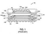
- FIG. 1illustrates a stacked-die device comprised of stacked sub-packages in accordance with the prior art.
- Stacked-die device 100shown in FIG. 1 includes three sub-packages 105 a, 105 b and 105 c, which may be stacked-die packages such as packages 105 b and 105 c.
- Package 105 aincludes a substrate 110 a with conductive balls 120 (e.g., ball grid array (BGA)) formed on the lower surface 111 of the substrate 110 a.
- the conductive balls 120are for electrically connecting the substrate 110 a to a motherboard (not shown).
- a die 130 ais disposed upon the upper surface 112 of the substrate 110 a.
- Package 105 bcomprises a stacked-die device having die 130 c stacked atop die 130 b.
- Package 105 ccomprises a stacked-die device having dies 130 d – 130 f stacked one atop the other as shown. All of the dies, 130 a, 130 b and 130 c, and 130 d – 130 f are electrically connected to respective substrates 110 a – 110 c or to one another with wire-bonds 140 .
- the wire-bonds 140 for each sub-packageare typically covered with a molding compound 145 for protection prior to stacking the sub-packages.
- the sub-packagesare electrically connected to each other with interconnections 150 , which may be copper joints between the sub-packages.
- the stacked-die device 100addresses some of the disadvantages of stack limitations and yield loss, but has disadvantages as well.
- the copper implants that form the connecting joints between sub-packagesrequire additional space. That is, the interconnections 150 between sub-packages have to be somewhat removed from the wire-bonds 140 so that they are not covered by the molding compound 145 . This increases the size of the stacked-die device.
- forming the copper implantsrequires additional processes (e.g., drilling), which increase the cost and practically limit the configuration of each package to a standard shape and size.
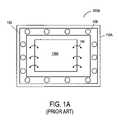
- FIG. 1Ais a top-down view of a sub-package for the stacked-die device 100 described above in reference to FIG. 1 . As shown in FIG.
- the copper implants 150 used to connect sub-packageshave a carrier 155 .
- the carrieris beyond the area on the substrate 110 a in which wire-bonds 140 may be placed.
- die 130 a, the substrate 110 a and hence the sub-package 105 aneed to be large enough to accommodate the carrier 155 .
- FIG. 1illustrates a stacked-die device comprised of stacked sub-packages in accordance with the prior art
- FIG. 1Ais a top-down view of a sub-package for a stacked-die device in accordance with the prior art
- FIG. 2illustrates top and side views of a substrate for a sub-package in accordance with one embodiment of the invention
- FIGS. 3A–3Dillustrate a process for producing a sub-package in accordance with one embodiment of the invention
- FIG. 4illustrates a process for encapsulating the dies of a sub-package while leaving an upper portion of the sub-package interconnections exposed in accordance with one embodiment of the invention
- FIG. 5illustrates a stacked-die device comprised of stacked sub-packages in accordance with one embodiment of the invention.
- FIG. 2illustrates top and side views of a substrate for a sub-package in accordance with one embodiment of the invention.
- the substrate 210has interconnections 240 and sub-package interconnections 250 that may be, for example, conductive metal balls, that can be used to electrically connect one sub-package to another sub-package above it in a stacked sub-package configuration.
- the sub-package interconnections 250may be similar to the BGA typically employed on the bottom side of a die for surface mount packaging.
- the sub-package interconnectionsare formed on the top-side (die side) of the substrate.
- the sub-package interconnections 250are discrete and therefore wire-bonding can be accomplished near and between the sub-package interconnections 250 .
- wire-bondscan be formed all the way up to where the sub-package interconnections will be placed.
- the sub-package interconnectionsare electrically connected to the die 230 through interconnections 240 .
- the bottom-side of the substratemay have a conventional BGA or metal lands for electrically connecting to the sub-package below.
- FIGS. 3A–3Dillustrate a process for producing a sub-package in accordance with one embodiment of the invention.
- substrate 310is a conventional substrate having features for die attach and wire-bonding, or flip chip attach.
- the bottom surface 311 of substrate 310has conductive metal balls 320 as described above in reference to FIG. 1 .
- the substrate 310has sub-package interconnections 350 formed on the top surface 312 .
- the sub-package interconnections 350are attached to metal pads (not shown) formed near the periphery of substrate 310 .
- the sub-package interconnections 350which may be conductive metal balls, may be formed of solder, which may be a lead/tin alloy.
- the sub-package interconnections 350may be made of copper or other suitable conductive metals.
- the sub-package interconnections 350may be attached using a process similar to a conventional BGA ball attach method.
- the diesmay implement various types of memory devices or logic processor devices.
- the dieswhich may be one die or multiple dies in a stacked-die configuration, are attached to the substrate 310 and to one another using conventional die attach methods and materials.
- die 330 ais attached to the top surface 312 of substrate 310 and die 330 b is stacked atop, and attached to, die 330 a.
- Each of the diesmay be electrically connected to the substrate and to one another using conventional methods (e.g., wire-bonding or flip chip attachment).
- the sub-package interconnections 350extend above the top surface 312 , a greater distance than the die stack.
- the attached die or die-stackis then encapsulated to protect the dies and associated wires (e.g., wire-bonds), if any, while leaving an upper portion 351 of the sub-package interconnections 350 exposed.
- the encapsulantextends above the upper surface 312 higher than the die stack, but not as high as the sub-package interconnections 350 .
- the encapsulant 345is a thermosetting material such as epoxy or polymer resin which may contain various amounts (e.g., from 0–80% by weight) of silica or other inorganic particles to modify the CTE, modulus, or viscosity.
- thermosetting materialmay contain fluxes to provide fluxing capabilities during a subsequent reflow process.
- the encapsulation of the die-stack, as shown in FIG. 3Cis effected through a stencil printing process described in greater detail below.
- the encapsulant 345may encompass the entire sub-package interconnections 350 .
- the sub-package interconnections 350may remain encapsulated where the sub-package is the top most sub-package of a stacked sub-package device. Where the sub-package interconnections will be used to electrically connect the sub-package to another sub-package above it in a stacked sub-package configuration, an upper portion of the sub-package interconnections 350 can be exposed through known methods such as grinding or laser drilling.
- Sub-packages that will be stacked atop another sub-packagemay not include conductive metal balls such as a BGA, but may include land pads 321 corresponding to the sub-package interconnections of the sub-package on which they are stacked.
- FIG. 4illustrates a process for encapsulating the dies of a sub-package while leaving an upper portion of the sub-package interconnections exposed in accordance with one embodiment of the invention.
- Process 400shown in FIG. 4 , begins at operation 405 in which a stencil is provided and placed over the substrate.
- the stencilwhich may be a thin nickel plate, is patterned to cover some upper portion of each of the sub-package interconnections.
- a stencil-printable encapsulantis provided.
- Typical encapsulantsare not stencil printable, but can be made so by decreasing their viscosity, for example by the addition of solvents to the encapsulation material.
- the stencil-printable encapsulantis applied to encapsulate the dies.
- the amount of encapsulantis controlled such that dies (e.g., die-stack) and associated wires are completely encapsulated while an upper portion of each of the sub-package interconnections is left exposed.
- the lower portion of the sub-package interconnectionsis also encapsulated.
- some of the encapsulantmay remain on the upper portions of the sub-package interconnections, but the low-viscosity encapsulant helps to reduce the amount of such encapsulant.
- the substrateis subjected to an elevated temperature in order to remove solvents (i.e., evaporate some or all of the solvents added in operation 410 ).
- the substrateis subjected to a temperature of approximately 100° C. for approximately 2 hours.
- the temperature and time for such an evaporation processmay be modified, depending upon the amount of solvents to be evaporated.
- the solvents, which aid in the stencil printing process,are removed as much as possible prior to reflow to reduce voids that may form during curing/reflow if the solvents are not removed. The removal of the solvents increases the viscosity of the applied encapsulant.
- the encapsulantis cured (cross linked) during a subsequent reflow process described more fully below.
- such curingis effected concurrently with the solder reflow.
- the curing kinetics of the encapsulantis specifically tailored so as to reduce interference with joint formation.
- Two or more sub-packagesare interconnected to form a stacked sub-package device in accordance with one embodiment of the invention.
- a sub-packageis stacked atop another such that land pads or conductive metal balls on the bottom side of the top most sub-package correspond to the exposed sub-package interconnections of the next lower sub-package in the stack.
- a reflow processor other conventional surface mount process, is then effected to create an interconnection between the sub-packages. During reflow, the viscosity of the encapsulant is decreased due to the increased temperature.
- FIG. 5illustrates a stacked-die device comprised of stacked sub-packages in accordance with one embodiment of the invention.
- Stacked-die device 500shown in FIG. 5 includes three sub-packages 505 a , 505 b and 505 c , which may be stacked-die sub-packages created in accordance with an embodiment of the invention.
- Sub-package 505 aincludes a substrate 510 a with conductive balls 520 .
- Sub-package 505 ahas dies 530 a and 530 b that are encapsulated with encapsulant 545 a .
- the upper portion 551 a of sub-package interconnections 550 aare exposed and form an interconnection with land pads 521 b formed on the bottom surface of sub-package 505 b .
- Sub-package 505 bhas dies 530 c and 530 d attached to substrate 510 b that are encapsulated with encapsulant 545 b .
- the upper portion 551 b of sub-package interconnections 550 bare exposed and form an interconnection with land pads 521 c formed on the bottom surface of sub-package 505 c .
- Sub-package 505 chas dies 530 e and 530 f attached to substrate 510 c that are encapsulated with encapsulant 545 c .
- the entire sub-package interconnections 550 care encapsulated as well.
- the stacked-die device 500is exemplary as are each of the stacked sub-packages of stacked-die device 500 .
- the stacked-die devicemay have any reasonable number of stacked sub-packages and each sub-package may have one die or any number of stacked die.
- Embodiments of the inventionprovide methods and apparatuses for producing a stacked die device having a stacked sub-package configuration.
- Various embodiments of the inventionhave been described including specific features or processes.
- the features or processesmay be modified.
- the sub-package interconnectionsalthough generally described as conductive metal balls, may be any suitable material or shape in accordance with alternative embodiments of the invention.
- process 400described above in reference to FIG. 4 , the operation of covering the sub-package interconnections may be omitted.
- the upper portion of the sub-package interconnectionsmay be exposed by dragging a squeegee across the surface of the applied encapsulant to expose the sub-package interconnections.
- the limited encapsulant material remaining on the surface of the sub-package interconnectionswill flow down off of the surface during reflow due to the increased viscosity of the encapsulant and the wetting between the sub-package interconnections and the corresponding land pads of the connecting sub-package.
- any residual encapsulantdoes not interfere with proper interconnection formation.
- a no-flow underfill materialmay be applied prior to reflow for better connection formation and thermal energy dissipation.
- the underfill materialmay be applied after the sub-packages have been connected.
Landscapes
- Engineering & Computer Science (AREA)
- Microelectronics & Electronic Packaging (AREA)
- Power Engineering (AREA)
- Computer Hardware Design (AREA)
- General Physics & Mathematics (AREA)
- Condensed Matter Physics & Semiconductors (AREA)
- Physics & Mathematics (AREA)
- Structures Or Materials For Encapsulating Or Coating Semiconductor Devices Or Solid State Devices (AREA)
- Combinations Of Printed Boards (AREA)
- Wire Bonding (AREA)
- Packaging Frangible Articles (AREA)
- Encapsulation Of And Coatings For Semiconductor Or Solid State Devices (AREA)
- Electric Connection Of Electric Components To Printed Circuits (AREA)
Abstract
Description
Claims (20)
Priority Applications (9)
| Application Number | Priority Date | Filing Date | Title |
|---|---|---|---|
| US10/917,142US7187068B2 (en) | 2004-08-11 | 2004-08-11 | Methods and apparatuses for providing stacked-die devices |
| TW094125491ATWI296151B (en) | 2004-08-11 | 2005-07-27 | Methods and apparatuses for providing stacked-die devices |
| DE112005001949.7TDE112005001949B4 (en) | 2004-08-11 | 2005-07-29 | Method for providing stacked chip elements |
| DE112005003862.9TDE112005003862B4 (en) | 2004-08-11 | 2005-07-29 | Device with a stencil for a screen printing process |
| JP2007525653AJP4610616B2 (en) | 2004-08-11 | 2005-07-29 | Method and apparatus for providing a die stack device |
| CN2005800269708ACN101002319B (en) | 2004-08-11 | 2005-07-29 | Methods and apparatuses for providing stacked-die devices |
| PCT/US2005/027103WO2006020438A1 (en) | 2004-08-11 | 2005-07-29 | Methods and apparatuses for providing stacked-die devices |
| HK08100138.5AHK1109678B (en) | 2004-08-11 | 2005-07-29 | Methods and apparatuses for providing stacked-die devices |
| US11/212,015US7867818B2 (en) | 2004-08-11 | 2005-08-24 | Methods and apparatuses for providing stacked-die devices |
Applications Claiming Priority (1)
| Application Number | Priority Date | Filing Date | Title |
|---|---|---|---|
| US10/917,142US7187068B2 (en) | 2004-08-11 | 2004-08-11 | Methods and apparatuses for providing stacked-die devices |
Related Child Applications (1)
| Application Number | Title | Priority Date | Filing Date |
|---|---|---|---|
| US11/212,015DivisionUS7867818B2 (en) | 2004-08-11 | 2005-08-24 | Methods and apparatuses for providing stacked-die devices |
Publications (2)
| Publication Number | Publication Date |
|---|---|
| US20060033193A1 US20060033193A1 (en) | 2006-02-16 |
| US7187068B2true US7187068B2 (en) | 2007-03-06 |
Family
ID=35355605
Family Applications (2)
| Application Number | Title | Priority Date | Filing Date |
|---|---|---|---|
| US10/917,142Expired - LifetimeUS7187068B2 (en) | 2004-08-11 | 2004-08-11 | Methods and apparatuses for providing stacked-die devices |
| US11/212,015Expired - LifetimeUS7867818B2 (en) | 2004-08-11 | 2005-08-24 | Methods and apparatuses for providing stacked-die devices |
Family Applications After (1)
| Application Number | Title | Priority Date | Filing Date |
|---|---|---|---|
| US11/212,015Expired - LifetimeUS7867818B2 (en) | 2004-08-11 | 2005-08-24 | Methods and apparatuses for providing stacked-die devices |
Country Status (6)
| Country | Link |
|---|---|
| US (2) | US7187068B2 (en) |
| JP (1) | JP4610616B2 (en) |
| CN (1) | CN101002319B (en) |
| DE (2) | DE112005003862B4 (en) |
| TW (1) | TWI296151B (en) |
| WO (1) | WO2006020438A1 (en) |
Cited By (41)
| Publication number | Priority date | Publication date | Assignee | Title |
|---|---|---|---|---|
| US20070034305A1 (en)* | 2005-08-12 | 2007-02-15 | Daewoong Suh | Bulk metallic glass solder material |
| US20070052081A1 (en)* | 2005-09-01 | 2007-03-08 | Gerber Mark A | Package-on-package semiconductor assembly |
| US20080073769A1 (en)* | 2006-09-27 | 2008-03-27 | Yen-Yi Wu | Semiconductor package and semiconductor device |
| US20080230887A1 (en)* | 2007-03-23 | 2008-09-25 | Advanced Semiconductor Engineering, Inc. | Semiconductor package and the method of making the same |
| US20090184412A1 (en)* | 2007-10-25 | 2009-07-23 | Rohm Co., Ltd. | Resin-seal type semiconductor device |
| US20090321908A1 (en)* | 2008-06-25 | 2009-12-31 | Sungmin Song | Stacked integrated circuit package system with intra-stack encapsulation |
| US20100000775A1 (en)* | 2008-07-03 | 2010-01-07 | Advanced Semiconductor Engineering, Inc. | Circuit substrate and method of fabricating the same and chip package structure |
| US20100171205A1 (en)* | 2009-01-07 | 2010-07-08 | Kuang-Hsiung Chen | Stackable Semiconductor Device Packages |
| US20100171207A1 (en)* | 2009-01-07 | 2010-07-08 | Chi-Chih Shen | Stackable semiconductor device packages |
| US20100171206A1 (en)* | 2009-01-07 | 2010-07-08 | Chi-Chih Chu | Package-on-Package Device, Semiconductor Package, and Method for Manufacturing The Same |
| US20110049704A1 (en)* | 2009-08-31 | 2011-03-03 | Advanced Semiconductor Engineering, Inc. | Semiconductor device packages with integrated heatsinks |
| US20110057308A1 (en)* | 2009-09-10 | 2011-03-10 | Daesik Choi | Integrated circuit packaging system with conductive pillars and method of manufacture thereof |
| US20110117700A1 (en)* | 2009-11-18 | 2011-05-19 | Advanced Semiconductor Engineering, Inc. | Stackable semiconductor device packages |
| US20110156251A1 (en)* | 2009-12-31 | 2011-06-30 | Chi-Chih Chu | Semiconductor Package |
| US20110193205A1 (en)* | 2010-02-10 | 2011-08-11 | Advanced Semiconductor Engineering, Inc. | Semiconductor device packages having stacking functionality and including interposer |
| US20110285007A1 (en)* | 2010-05-24 | 2011-11-24 | Stats Chippac, Ltd. | Semiconductor Device and Method of Forming Ultra Thin Multi-Die Face-to-Face WLCSP |
| US8125066B1 (en)* | 2009-07-13 | 2012-02-28 | Altera Corporation | Package on package configurations with embedded solder balls and interposal layer |
| US20120061855A1 (en)* | 2010-09-14 | 2012-03-15 | Byung Tai Do | Integrated circuit packaging system with film encapsulation and method of manufacture thereof |
| US20120104590A1 (en)* | 2010-11-02 | 2012-05-03 | Stats Chippac, Ltd. | Semiconductor Device and Method of Forming Penetrable Film Encapsulant Around Semiconductor Die and Interconnect Structure |
| US8227905B1 (en)* | 2004-06-08 | 2012-07-24 | Amkor Technology, Inc. | Stackable semiconductor package |
| US8278746B2 (en) | 2010-04-02 | 2012-10-02 | Advanced Semiconductor Engineering, Inc. | Semiconductor device packages including connecting elements |
| US8569885B2 (en) | 2010-10-29 | 2013-10-29 | Advanced Semiconductor Engineering, Inc. | Stacked semiconductor packages and related methods |
| US8624374B2 (en) | 2010-04-02 | 2014-01-07 | Advanced Semiconductor Engineering, Inc. | Semiconductor device packages with fan-out and with connecting elements for stacking and manufacturing methods thereof |
| US8643167B2 (en) | 2011-01-06 | 2014-02-04 | Advanced Semiconductor Engineering, Inc. | Semiconductor package with through silicon vias and method for making the same |
| US8952517B2 (en) | 2012-06-28 | 2015-02-10 | Samsung Electronics Co., Ltd. | Package-on-package device and method of fabricating the same |
| US8987058B2 (en) | 2013-03-12 | 2015-03-24 | Taiwan Semiconductor Manufacturing Company, Ltd. | Method for wafer separation |
| US9082776B2 (en) | 2012-08-24 | 2015-07-14 | Taiwan Semiconductor Manufacturing Company, Ltd. | Semiconductor package having protective layer with curved surface and method of manufacturing same |
| US9171792B2 (en) | 2011-02-28 | 2015-10-27 | Advanced Semiconductor Engineering, Inc. | Semiconductor device packages having a side-by-side device arrangement and stacking functionality |
| US9196597B2 (en) | 2010-01-13 | 2015-11-24 | Advanced Semiconductor Engineering, Inc. | Semiconductor package with single sided substrate design and manufacturing methods thereof |
| US9240387B2 (en) | 2011-10-12 | 2016-01-19 | Taiwan Semiconductor Manufacturing Company, Ltd. | Wafer-level chip scale package with re-workable underfill |
| US9257333B2 (en) | 2013-03-11 | 2016-02-09 | Taiwan Semiconductor Manufacturing Company, Ltd. | Interconnect structures and methods of forming same |
| US9263839B2 (en) | 2012-12-28 | 2016-02-16 | Taiwan Semiconductor Manufacturing Company, Ltd. | System and method for an improved fine pitch joint |
| US9287143B2 (en) | 2012-01-12 | 2016-03-15 | Taiwan Semiconductor Manufacturing Company, Ltd. | Apparatus for package reinforcement using molding underfill |
| US9349611B2 (en) | 2010-03-22 | 2016-05-24 | Advanced Semiconductor Engineering, Inc. | Stackable semiconductor package and manufacturing method thereof |
| US9368398B2 (en) | 2012-01-12 | 2016-06-14 | Taiwan Semiconductor Manufacturing Company, Ltd. | Interconnect structure and method of fabricating same |
| US9401308B2 (en) | 2013-03-12 | 2016-07-26 | Taiwan Semiconductor Manufacturing Company, Ltd. | Packaging devices, methods of manufacture thereof, and packaging methods |
| US9437564B2 (en) | 2013-07-09 | 2016-09-06 | Taiwan Semiconductor Manufacturing Company, Ltd. | Interconnect structure and method of fabricating same |
| US9589862B2 (en) | 2013-03-11 | 2017-03-07 | Taiwan Semiconductor Manufacturing Company, Ltd. | Interconnect structures and methods of forming same |
| US9607921B2 (en) | 2012-01-12 | 2017-03-28 | Taiwan Semiconductor Manufacturing Company, Ltd. | Package on package interconnect structure |
| US9892962B2 (en) | 2015-11-30 | 2018-02-13 | Taiwan Semiconductor Manufacturing Company, Ltd. | Wafer level chip scale package interconnects and methods of manufacture thereof |
| US10015888B2 (en) | 2013-02-15 | 2018-07-03 | Taiwan Semiconductor Manufacturing Company, Ltd. | Interconnect joint protective layer apparatus and method |
Families Citing this family (19)
| Publication number | Priority date | Publication date | Assignee | Title |
|---|---|---|---|---|
| US7875966B2 (en)* | 2005-02-14 | 2011-01-25 | Stats Chippac Ltd. | Stacked integrated circuit and package system |
| US7265442B2 (en)* | 2005-03-21 | 2007-09-04 | Nokia Corporation | Stacked package integrated circuit |
| US20080054431A1 (en)* | 2006-08-31 | 2008-03-06 | Tingqing Wang | Embedded package in package |
| JP2008235401A (en)* | 2007-03-19 | 2008-10-02 | Spansion Llc | Semiconductor device and manufacturing method therefor |
| US8049320B2 (en) | 2008-02-19 | 2011-11-01 | Texas Instruments Incorporated | Integrated circuit stacked package precursors and stacked packaged devices and systems therefrom |
| CN101728354B (en)* | 2008-10-27 | 2013-07-10 | 松下电器产业株式会社 | Electronic device and manufacturing method for electronic device |
| CN101894829B (en)* | 2009-05-19 | 2012-06-27 | 国碁电子(中山)有限公司 | Stacked encapsulating structure |
| US8742603B2 (en)* | 2010-05-20 | 2014-06-03 | Qualcomm Incorporated | Process for improving package warpage and connection reliability through use of a backside mold configuration (BSMC) |
| US8039275B1 (en)* | 2010-06-02 | 2011-10-18 | Stats Chippac Ltd. | Integrated circuit packaging system with rounded interconnect and method of manufacture thereof |
| US8754516B2 (en) | 2010-08-26 | 2014-06-17 | Intel Corporation | Bumpless build-up layer package with pre-stacked microelectronic devices |
| US8927391B2 (en)* | 2011-05-27 | 2015-01-06 | Taiwan Semiconductor Manufacturing Company, Ltd. | Package-on-package process for applying molding compound |
| US8461676B2 (en) | 2011-09-09 | 2013-06-11 | Qualcomm Incorporated | Soldering relief method and semiconductor device employing same |
| US8664040B2 (en)* | 2011-12-20 | 2014-03-04 | Taiwan Semiconductor Manufacturing Company, Ltd. | Exposing connectors in packages through selective treatment |
| KR20130089473A (en)* | 2012-02-02 | 2013-08-12 | 삼성전자주식회사 | Semiconductor package |
| US9385006B2 (en)* | 2012-06-21 | 2016-07-05 | STATS ChipPAC Pte. Ltd. | Semiconductor device and method of forming an embedded SOP fan-out package |
| TWI601252B (en)* | 2015-05-22 | 2017-10-01 | 南茂科技股份有限公司 | Manufacturing method of package structure and package structure manufactured by the same |
| TWI622139B (en)* | 2016-03-08 | 2018-04-21 | 恆勁科技股份有限公司 | Package substrate |
| US9859253B1 (en)* | 2016-06-29 | 2018-01-02 | Intel Corporation | Integrated circuit package stack |
| US20220406751A1 (en)* | 2021-06-22 | 2022-12-22 | Intel Corporation | Quasi-monolithic hierarchical integration architecture |
Citations (11)
| Publication number | Priority date | Publication date | Assignee | Title |
|---|---|---|---|---|
| US5040052A (en) | 1987-12-28 | 1991-08-13 | Texas Instruments Incorporated | Compact silicon module for high density integrated circuits |
| US5422435A (en) | 1992-05-22 | 1995-06-06 | National Semiconductor Corporation | Stacked multi-chip modules and method of manufacturing |
| JP2000178414A (en)* | 1998-12-16 | 2000-06-27 | Tokuyama Corp | Spherical silica for semiconductor encapsulant |
| JP2001223227A (en)* | 2000-02-08 | 2001-08-17 | Nitto Denko Corp | Resin composition for semiconductor encapsulation and semiconductor device |
| US6414384B1 (en)* | 2000-12-22 | 2002-07-02 | Silicon Precision Industries Co., Ltd. | Package structure stacking chips on front surface and back surface of substrate |
| US20020121687A1 (en) | 2001-03-02 | 2002-09-05 | Johann Winderl | Electronic component with stacked semiconductor chips |
| US6448506B1 (en) | 2000-12-28 | 2002-09-10 | Amkor Technology, Inc. | Semiconductor package and circuit board for making the package |
| US20020135057A1 (en) | 2001-03-26 | 2002-09-26 | Yoichiro Kurita | Thin planar semiconductor device having electrodes on both surfaces and method of fabricating same |
| US6489676B2 (en) | 2000-12-04 | 2002-12-03 | Fujitsu Limited | Semiconductor device having an interconnecting post formed on an interposer within a sealing resin |
| US20020196650A1 (en) | 1999-12-10 | 2002-12-26 | Nai-Shung Chang | Mother board and computer system capable of flexibly using synchronous dynamic random access memory and double data rate dynamic random access memory |
| US20050121764A1 (en)* | 2003-12-04 | 2005-06-09 | Debendra Mallik | Stackable integrated circuit packaging |
Family Cites Families (15)
| Publication number | Priority date | Publication date | Assignee | Title |
|---|---|---|---|---|
| JPH07335783A (en)* | 1994-06-13 | 1995-12-22 | Fujitsu Ltd | Semiconductor device and semiconductor device unit |
| US6194250B1 (en)* | 1998-09-14 | 2001-02-27 | Motorola, Inc. | Low-profile microelectronic package |
| JP3500995B2 (en)* | 1998-12-18 | 2004-02-23 | 株式会社デンソー | Manufacturing method of laminated circuit module |
| TW434850B (en)* | 1998-12-31 | 2001-05-16 | World Wiser Electronics Inc | Packaging equipment and method for integrated circuit |
| US6326555B1 (en)* | 1999-02-26 | 2001-12-04 | Fujitsu Limited | Method and structure of z-connected laminated substrate for high density electronic packaging |
| JP3798597B2 (en)* | 1999-11-30 | 2006-07-19 | 富士通株式会社 | Semiconductor device |
| JP3916854B2 (en)* | 2000-06-28 | 2007-05-23 | シャープ株式会社 | Wiring board, semiconductor device, and package stack semiconductor device |
| TW461058B (en) | 2000-10-19 | 2001-10-21 | Siliconware Precision Industries Co Ltd | Stacked multi-chip package structure with integrated passive components |
| JP4483136B2 (en)* | 2001-06-20 | 2010-06-16 | ソニー株式会社 | Semiconductor device mounting method and semiconductor device manufacturing method |
| US6730536B1 (en)* | 2001-06-28 | 2004-05-04 | Amkor Technology, Inc. | Pre-drilled image sensor package fabrication method |
| JP3781998B2 (en)* | 2001-10-30 | 2006-06-07 | シャープ株式会社 | Manufacturing method of stacked semiconductor device |
| JP3972182B2 (en)* | 2002-03-05 | 2007-09-05 | セイコーエプソン株式会社 | Manufacturing method of semiconductor device |
| AU2003298595A1 (en)* | 2002-10-08 | 2004-05-04 | Chippac, Inc. | Semiconductor stacked multi-package module having inverted second package |
| JP2004327855A (en)* | 2003-04-25 | 2004-11-18 | Nec Electronics Corp | Semiconductor device and its manufacturing method |
| US20040262728A1 (en)* | 2003-06-30 | 2004-12-30 | Sterrett Terry L. | Modular device assemblies |
- 2004
- 2004-08-11USUS10/917,142patent/US7187068B2/ennot_activeExpired - Lifetime
- 2005
- 2005-07-27TWTW094125491Apatent/TWI296151B/ennot_activeIP Right Cessation
- 2005-07-29JPJP2007525653Apatent/JP4610616B2/ennot_activeExpired - Fee Related
- 2005-07-29DEDE112005003862.9Tpatent/DE112005003862B4/ennot_activeExpired - Fee Related
- 2005-07-29DEDE112005001949.7Tpatent/DE112005001949B4/ennot_activeExpired - Fee Related
- 2005-07-29CNCN2005800269708Apatent/CN101002319B/ennot_activeExpired - Fee Related
- 2005-07-29WOPCT/US2005/027103patent/WO2006020438A1/enactiveApplication Filing
- 2005-08-24USUS11/212,015patent/US7867818B2/ennot_activeExpired - Lifetime
Patent Citations (13)
| Publication number | Priority date | Publication date | Assignee | Title |
|---|---|---|---|---|
| US5040052A (en) | 1987-12-28 | 1991-08-13 | Texas Instruments Incorporated | Compact silicon module for high density integrated circuits |
| US5422435A (en) | 1992-05-22 | 1995-06-06 | National Semiconductor Corporation | Stacked multi-chip modules and method of manufacturing |
| JP2000178414A (en)* | 1998-12-16 | 2000-06-27 | Tokuyama Corp | Spherical silica for semiconductor encapsulant |
| US20020196650A1 (en) | 1999-12-10 | 2002-12-26 | Nai-Shung Chang | Mother board and computer system capable of flexibly using synchronous dynamic random access memory and double data rate dynamic random access memory |
| US6813157B2 (en) | 1999-12-10 | 2004-11-02 | Via Technologies, Inc. | Mother board and computer system capable of flexibly using synchronous dynamic random access memory and double data rate dynamic random access memory |
| JP2001223227A (en)* | 2000-02-08 | 2001-08-17 | Nitto Denko Corp | Resin composition for semiconductor encapsulation and semiconductor device |
| US6489676B2 (en) | 2000-12-04 | 2002-12-03 | Fujitsu Limited | Semiconductor device having an interconnecting post formed on an interposer within a sealing resin |
| US20030042564A1 (en) | 2000-12-04 | 2003-03-06 | Fujitsu Limited | Semiconductor device having an interconnecting post formed on an interposer within a sealing resin |
| US6414384B1 (en)* | 2000-12-22 | 2002-07-02 | Silicon Precision Industries Co., Ltd. | Package structure stacking chips on front surface and back surface of substrate |
| US6448506B1 (en) | 2000-12-28 | 2002-09-10 | Amkor Technology, Inc. | Semiconductor package and circuit board for making the package |
| US20020121687A1 (en) | 2001-03-02 | 2002-09-05 | Johann Winderl | Electronic component with stacked semiconductor chips |
| US20020135057A1 (en) | 2001-03-26 | 2002-09-26 | Yoichiro Kurita | Thin planar semiconductor device having electrodes on both surfaces and method of fabricating same |
| US20050121764A1 (en)* | 2003-12-04 | 2005-06-09 | Debendra Mallik | Stackable integrated circuit packaging |
Non-Patent Citations (1)
| Title |
|---|
| PCT Search Report mailed Dec. 6, 2005 for PCT/US2005/027103. |
Cited By (71)
| Publication number | Priority date | Publication date | Assignee | Title |
|---|---|---|---|---|
| US8466545B1 (en) | 2004-06-08 | 2013-06-18 | Amkor Technology, Inc. | Stackable semiconductor package |
| US8227905B1 (en)* | 2004-06-08 | 2012-07-24 | Amkor Technology, Inc. | Stackable semiconductor package |
| US7628871B2 (en) | 2005-08-12 | 2009-12-08 | Intel Corporation | Bulk metallic glass solder material |
| US20070034305A1 (en)* | 2005-08-12 | 2007-02-15 | Daewoong Suh | Bulk metallic glass solder material |
| US7675152B2 (en)* | 2005-09-01 | 2010-03-09 | Texas Instruments Incorporated | Package-on-package semiconductor assembly |
| US20070052081A1 (en)* | 2005-09-01 | 2007-03-08 | Gerber Mark A | Package-on-package semiconductor assembly |
| US20080076208A1 (en)* | 2006-09-27 | 2008-03-27 | Yen-Yi Wu | Method of making a semiconductor package and method of making a semiconductor device |
| US7642133B2 (en) | 2006-09-27 | 2010-01-05 | Advanced Semiconductor Engineering, Inc. | Method of making a semiconductor package and method of making a semiconductor device |
| US20080073769A1 (en)* | 2006-09-27 | 2008-03-27 | Yen-Yi Wu | Semiconductor package and semiconductor device |
| US20080230887A1 (en)* | 2007-03-23 | 2008-09-25 | Advanced Semiconductor Engineering, Inc. | Semiconductor package and the method of making the same |
| US8143101B2 (en)* | 2007-03-23 | 2012-03-27 | Advanced Semiconductor Engineering, Inc. | Semiconductor package and the method of making the same |
| US20090184412A1 (en)* | 2007-10-25 | 2009-07-23 | Rohm Co., Ltd. | Resin-seal type semiconductor device |
| US9484282B2 (en)* | 2007-10-25 | 2016-11-01 | Rohm Co., Ltd. | Resin-sealed semiconductor device |
| US20090321908A1 (en)* | 2008-06-25 | 2009-12-31 | Sungmin Song | Stacked integrated circuit package system with intra-stack encapsulation |
| US7871861B2 (en)* | 2008-06-25 | 2011-01-18 | Stats Chippac Ltd. | Stacked integrated circuit package system with intra-stack encapsulation |
| US20100000775A1 (en)* | 2008-07-03 | 2010-01-07 | Advanced Semiconductor Engineering, Inc. | Circuit substrate and method of fabricating the same and chip package structure |
| US8158888B2 (en) | 2008-07-03 | 2012-04-17 | Advanced Semiconductor Engineering, Inc. | Circuit substrate and method of fabricating the same and chip package structure |
| US8076765B2 (en) | 2009-01-07 | 2011-12-13 | Advanced Semiconductor Engineering, Inc. | Stackable semiconductor device packages including openings partially exposing connecting elements, conductive bumps, or conductive conductors |
| US20100171207A1 (en)* | 2009-01-07 | 2010-07-08 | Chi-Chih Shen | Stackable semiconductor device packages |
| US20100171206A1 (en)* | 2009-01-07 | 2010-07-08 | Chi-Chih Chu | Package-on-Package Device, Semiconductor Package, and Method for Manufacturing The Same |
| US8012797B2 (en) | 2009-01-07 | 2011-09-06 | Advanced Semiconductor Engineering, Inc. | Method for forming stackable semiconductor device packages including openings with conductive bumps of specified geometries |
| US20100171205A1 (en)* | 2009-01-07 | 2010-07-08 | Kuang-Hsiung Chen | Stackable Semiconductor Device Packages |
| US8125066B1 (en)* | 2009-07-13 | 2012-02-28 | Altera Corporation | Package on package configurations with embedded solder balls and interposal layer |
| US20110049704A1 (en)* | 2009-08-31 | 2011-03-03 | Advanced Semiconductor Engineering, Inc. | Semiconductor device packages with integrated heatsinks |
| US20110057308A1 (en)* | 2009-09-10 | 2011-03-10 | Daesik Choi | Integrated circuit packaging system with conductive pillars and method of manufacture thereof |
| US20110180935A1 (en)* | 2009-09-10 | 2011-07-28 | Daesik Choi | Integrated circuit packaging system with conductive pillars and method of manufacture thereof |
| US7923304B2 (en) | 2009-09-10 | 2011-04-12 | Stats Chippac Ltd. | Integrated circuit packaging system with conductive pillars and method of manufacture thereof |
| US8232141B2 (en) | 2009-09-10 | 2012-07-31 | Stats Chippac Ltd. | Integrated circuit packaging system with conductive pillars and method of manufacture thereof |
| US20110117700A1 (en)* | 2009-11-18 | 2011-05-19 | Advanced Semiconductor Engineering, Inc. | Stackable semiconductor device packages |
| US8198131B2 (en) | 2009-11-18 | 2012-06-12 | Advanced Semiconductor Engineering, Inc. | Stackable semiconductor device packages |
| US8405212B2 (en) | 2009-12-31 | 2013-03-26 | Advanced Semiconductor Engineering, Inc. | Semiconductor package |
| US20110156251A1 (en)* | 2009-12-31 | 2011-06-30 | Chi-Chih Chu | Semiconductor Package |
| US9196597B2 (en) | 2010-01-13 | 2015-11-24 | Advanced Semiconductor Engineering, Inc. | Semiconductor package with single sided substrate design and manufacturing methods thereof |
| US20110193205A1 (en)* | 2010-02-10 | 2011-08-11 | Advanced Semiconductor Engineering, Inc. | Semiconductor device packages having stacking functionality and including interposer |
| US8823156B2 (en) | 2010-02-10 | 2014-09-02 | Advanced Semiconductor Engineering, Inc. | Semiconductor device packages having stacking functionality and including interposer |
| US9349611B2 (en) | 2010-03-22 | 2016-05-24 | Advanced Semiconductor Engineering, Inc. | Stackable semiconductor package and manufacturing method thereof |
| US8278746B2 (en) | 2010-04-02 | 2012-10-02 | Advanced Semiconductor Engineering, Inc. | Semiconductor device packages including connecting elements |
| US8624374B2 (en) | 2010-04-02 | 2014-01-07 | Advanced Semiconductor Engineering, Inc. | Semiconductor device packages with fan-out and with connecting elements for stacking and manufacturing methods thereof |
| US10573600B2 (en) | 2010-05-24 | 2020-02-25 | STATS ChipPAC Pte. Ltd. | Semiconductor device and method of forming ultra thin multi-die face-to-face WLCSP |
| US9735113B2 (en)* | 2010-05-24 | 2017-08-15 | STATS ChipPAC Pte. Ltd. | Semiconductor device and method of forming ultra thin multi-die face-to-face WLCSP |
| US20110285007A1 (en)* | 2010-05-24 | 2011-11-24 | Stats Chippac, Ltd. | Semiconductor Device and Method of Forming Ultra Thin Multi-Die Face-to-Face WLCSP |
| US20120061855A1 (en)* | 2010-09-14 | 2012-03-15 | Byung Tai Do | Integrated circuit packaging system with film encapsulation and method of manufacture thereof |
| US8378477B2 (en)* | 2010-09-14 | 2013-02-19 | Stats Chippac Ltd. | Integrated circuit packaging system with film encapsulation and method of manufacture thereof |
| US8569885B2 (en) | 2010-10-29 | 2013-10-29 | Advanced Semiconductor Engineering, Inc. | Stacked semiconductor packages and related methods |
| US8546193B2 (en)* | 2010-11-02 | 2013-10-01 | Stats Chippac, Ltd. | Semiconductor device and method of forming penetrable film encapsulant around semiconductor die and interconnect structure |
| US20120104590A1 (en)* | 2010-11-02 | 2012-05-03 | Stats Chippac, Ltd. | Semiconductor Device and Method of Forming Penetrable Film Encapsulant Around Semiconductor Die and Interconnect Structure |
| US9431331B2 (en) | 2010-11-02 | 2016-08-30 | STATS ChipPAC Pte. Ltd. | Semiconductor device and method of forming penetrable film encapsulant around semiconductor die and interconnect structure |
| US8643167B2 (en) | 2011-01-06 | 2014-02-04 | Advanced Semiconductor Engineering, Inc. | Semiconductor package with through silicon vias and method for making the same |
| US9171792B2 (en) | 2011-02-28 | 2015-10-27 | Advanced Semiconductor Engineering, Inc. | Semiconductor device packages having a side-by-side device arrangement and stacking functionality |
| US9240387B2 (en) | 2011-10-12 | 2016-01-19 | Taiwan Semiconductor Manufacturing Company, Ltd. | Wafer-level chip scale package with re-workable underfill |
| US9287143B2 (en) | 2012-01-12 | 2016-03-15 | Taiwan Semiconductor Manufacturing Company, Ltd. | Apparatus for package reinforcement using molding underfill |
| US9368398B2 (en) | 2012-01-12 | 2016-06-14 | Taiwan Semiconductor Manufacturing Company, Ltd. | Interconnect structure and method of fabricating same |
| US9607921B2 (en) | 2012-01-12 | 2017-03-28 | Taiwan Semiconductor Manufacturing Company, Ltd. | Package on package interconnect structure |
| US9768136B2 (en) | 2012-01-12 | 2017-09-19 | Taiwan Semiconductor Manufacturing Company, Ltd. | Interconnect structure and method of fabricating same |
| US8952517B2 (en) | 2012-06-28 | 2015-02-10 | Samsung Electronics Co., Ltd. | Package-on-package device and method of fabricating the same |
| US9698028B2 (en) | 2012-08-24 | 2017-07-04 | Taiwan Semiconductor Manufacturing Company, Ltd. | Semiconductor package and method of manufacturing the same |
| US9082776B2 (en) | 2012-08-24 | 2015-07-14 | Taiwan Semiconductor Manufacturing Company, Ltd. | Semiconductor package having protective layer with curved surface and method of manufacturing same |
| US10062659B2 (en) | 2012-12-28 | 2018-08-28 | Taiwan Semiconductor Manufacturing Company, Ltd. | System and method for an improved fine pitch joint |
| US9263839B2 (en) | 2012-12-28 | 2016-02-16 | Taiwan Semiconductor Manufacturing Company, Ltd. | System and method for an improved fine pitch joint |
| US10015888B2 (en) | 2013-02-15 | 2018-07-03 | Taiwan Semiconductor Manufacturing Company, Ltd. | Interconnect joint protective layer apparatus and method |
| US9935070B2 (en) | 2013-03-11 | 2018-04-03 | Taiwan Semiconductor Manufacturing Company, Ltd. | Interconnect structures and methods of forming same |
| US9589862B2 (en) | 2013-03-11 | 2017-03-07 | Taiwan Semiconductor Manufacturing Company, Ltd. | Interconnect structures and methods of forming same |
| US10262964B2 (en) | 2013-03-11 | 2019-04-16 | Taiwan Semiconductor Manufacturing Company, Ltd. | Interconnect structures and methods of forming same |
| US9257333B2 (en) | 2013-03-11 | 2016-02-09 | Taiwan Semiconductor Manufacturing Company, Ltd. | Interconnect structures and methods of forming same |
| US10714442B2 (en) | 2013-03-11 | 2020-07-14 | Taiwan Semiconductor Manufacturing Company, Ltd. | Interconnect structures and methods of forming same |
| US11043463B2 (en) | 2013-03-11 | 2021-06-22 | Taiwan Semiconductor Manufacturing Company, Ltd. | Interconnect structures and methods of forming same |
| US8987058B2 (en) | 2013-03-12 | 2015-03-24 | Taiwan Semiconductor Manufacturing Company, Ltd. | Method for wafer separation |
| US9673160B2 (en) | 2013-03-12 | 2017-06-06 | Taiwan Semiconductor Manufacturing Company, Ltd. | Packaging devices, methods of manufacture thereof, and packaging methods |
| US9401308B2 (en) | 2013-03-12 | 2016-07-26 | Taiwan Semiconductor Manufacturing Company, Ltd. | Packaging devices, methods of manufacture thereof, and packaging methods |
| US9437564B2 (en) | 2013-07-09 | 2016-09-06 | Taiwan Semiconductor Manufacturing Company, Ltd. | Interconnect structure and method of fabricating same |
| US9892962B2 (en) | 2015-11-30 | 2018-02-13 | Taiwan Semiconductor Manufacturing Company, Ltd. | Wafer level chip scale package interconnects and methods of manufacture thereof |
Also Published As
| Publication number | Publication date |
|---|---|
| DE112005001949B4 (en) | 2014-11-27 |
| US20060035409A1 (en) | 2006-02-16 |
| TWI296151B (en) | 2008-04-21 |
| US20060033193A1 (en) | 2006-02-16 |
| CN101002319B (en) | 2011-08-17 |
| US7867818B2 (en) | 2011-01-11 |
| DE112005001949T5 (en) | 2007-05-31 |
| WO2006020438A1 (en) | 2006-02-23 |
| HK1109678A1 (en) | 2008-06-13 |
| DE112005003862B4 (en) | 2016-07-21 |
| TW200618253A (en) | 2006-06-01 |
| JP2008510304A (en) | 2008-04-03 |
| JP4610616B2 (en) | 2011-01-12 |
| CN101002319A (en) | 2007-07-18 |
| DE112005003862A5 (en) | 2014-09-18 |
Similar Documents
| Publication | Publication Date | Title |
|---|---|---|
| US7187068B2 (en) | Methods and apparatuses for providing stacked-die devices | |
| US11424211B2 (en) | Package-on-package assembly with wire bonds to encapsulation surface | |
| US10541213B2 (en) | Backside redistribution layer (RDL) structure | |
| US8922005B2 (en) | Methods and apparatus for package on package devices with reversed stud bump through via interconnections | |
| US8426246B2 (en) | Vented die and package | |
| US8618659B2 (en) | Package-on-package assembly with wire bonds to encapsulation surface | |
| US20070254406A1 (en) | Method for manufacturing stacked package structure | |
| TWI469301B (en) | Semiconductor multi-package module having wire bond interconnection between stacked packages | |
| US8399985B2 (en) | Mold design and semiconductor package | |
| US20080283994A1 (en) | Stacked package structure and fabrication method thereof | |
| US20210272880A1 (en) | Semiconductor package including composite molding structure | |
| US20220375891A1 (en) | Package-on-package assembly with wire bonds to encapsulation surface | |
| KR100865046B1 (en) | Methods and apparatuses for providing stacked die devices | |
| KR101096440B1 (en) | Dual die package | |
| KR20070090618A (en) | Manufacturing method of stack package | |
| KR101123797B1 (en) | Semiconductor package and stacked semiconductor package having the same | |
| US20250323107A1 (en) | Method of forming semiconductor device | |
| HK1109678B (en) | Methods and apparatuses for providing stacked-die devices | |
| KR20240062251A (en) | Semiconductor package and method for fabricating the same | |
| CN118352323A (en) | Semiconductor packaging | |
| KR20040091985A (en) | Ball Grid Array Package |
Legal Events
| Date | Code | Title | Description |
|---|---|---|---|
| AS | Assignment | Owner name:INTEL CORPORATION, CALIFORNIA Free format text:ASSIGNMENT OF ASSIGNORS INTEREST;ASSIGNORS:SUH, DAEWOONG;MALLIK, DEBENDRA;REEL/FRAME:015958/0377 Effective date:20041101 | |
| STCF | Information on status: patent grant | Free format text:PATENTED CASE | |
| FPAY | Fee payment | Year of fee payment:4 | |
| AS | Assignment | Owner name:MICRON TECHNOLOGY, INC., IDAHO Free format text:ASSIGNMENT OF ASSIGNORS INTEREST;ASSIGNOR:INTEL CORPORATION;REEL/FRAME:030740/0823 Effective date:20111122 | |
| FPAY | Fee payment | Year of fee payment:8 | |
| AS | Assignment | Owner name:U.S. BANK NATIONAL ASSOCIATION, AS COLLATERAL AGENT, CALIFORNIA Free format text:SECURITY INTEREST;ASSIGNOR:MICRON TECHNOLOGY, INC.;REEL/FRAME:038669/0001 Effective date:20160426 Owner name:U.S. BANK NATIONAL ASSOCIATION, AS COLLATERAL AGEN Free format text:SECURITY INTEREST;ASSIGNOR:MICRON TECHNOLOGY, INC.;REEL/FRAME:038669/0001 Effective date:20160426 | |
| AS | Assignment | Owner name:MORGAN STANLEY SENIOR FUNDING, INC., AS COLLATERAL AGENT, MARYLAND Free format text:PATENT SECURITY AGREEMENT;ASSIGNOR:MICRON TECHNOLOGY, INC.;REEL/FRAME:038954/0001 Effective date:20160426 Owner name:MORGAN STANLEY SENIOR FUNDING, INC., AS COLLATERAL Free format text:PATENT SECURITY AGREEMENT;ASSIGNOR:MICRON TECHNOLOGY, INC.;REEL/FRAME:038954/0001 Effective date:20160426 | |
| AS | Assignment | Owner name:U.S. BANK NATIONAL ASSOCIATION, AS COLLATERAL AGENT, CALIFORNIA Free format text:CORRECTIVE ASSIGNMENT TO CORRECT THE REPLACE ERRONEOUSLY FILED PATENT #7358718 WITH THE CORRECT PATENT #7358178 PREVIOUSLY RECORDED ON REEL 038669 FRAME 0001. ASSIGNOR(S) HEREBY CONFIRMS THE SECURITY INTEREST;ASSIGNOR:MICRON TECHNOLOGY, INC.;REEL/FRAME:043079/0001 Effective date:20160426 Owner name:U.S. BANK NATIONAL ASSOCIATION, AS COLLATERAL AGEN Free format text:CORRECTIVE ASSIGNMENT TO CORRECT THE REPLACE ERRONEOUSLY FILED PATENT #7358718 WITH THE CORRECT PATENT #7358178 PREVIOUSLY RECORDED ON REEL 038669 FRAME 0001. ASSIGNOR(S) HEREBY CONFIRMS THE SECURITY INTEREST;ASSIGNOR:MICRON TECHNOLOGY, INC.;REEL/FRAME:043079/0001 Effective date:20160426 | |
| AS | Assignment | Owner name:JPMORGAN CHASE BANK, N.A., AS COLLATERAL AGENT, ILLINOIS Free format text:SECURITY INTEREST;ASSIGNORS:MICRON TECHNOLOGY, INC.;MICRON SEMICONDUCTOR PRODUCTS, INC.;REEL/FRAME:047540/0001 Effective date:20180703 Owner name:JPMORGAN CHASE BANK, N.A., AS COLLATERAL AGENT, IL Free format text:SECURITY INTEREST;ASSIGNORS:MICRON TECHNOLOGY, INC.;MICRON SEMICONDUCTOR PRODUCTS, INC.;REEL/FRAME:047540/0001 Effective date:20180703 | |
| AS | Assignment | Owner name:MICRON TECHNOLOGY, INC., IDAHO Free format text:RELEASE BY SECURED PARTY;ASSIGNOR:U.S. BANK NATIONAL ASSOCIATION, AS COLLATERAL AGENT;REEL/FRAME:047243/0001 Effective date:20180629 | |
| MAFP | Maintenance fee payment | Free format text:PAYMENT OF MAINTENANCE FEE, 12TH YEAR, LARGE ENTITY (ORIGINAL EVENT CODE: M1553); ENTITY STATUS OF PATENT OWNER: LARGE ENTITY Year of fee payment:12 | |
| AS | Assignment | Owner name:MICRON TECHNOLOGY, INC., IDAHO Free format text:RELEASE BY SECURED PARTY;ASSIGNOR:MORGAN STANLEY SENIOR FUNDING, INC., AS COLLATERAL AGENT;REEL/FRAME:050937/0001 Effective date:20190731 | |
| AS | Assignment | Owner name:MICRON TECHNOLOGY, INC., IDAHO Free format text:RELEASE BY SECURED PARTY;ASSIGNOR:JPMORGAN CHASE BANK, N.A., AS COLLATERAL AGENT;REEL/FRAME:051028/0001 Effective date:20190731 Owner name:MICRON SEMICONDUCTOR PRODUCTS, INC., IDAHO Free format text:RELEASE BY SECURED PARTY;ASSIGNOR:JPMORGAN CHASE BANK, N.A., AS COLLATERAL AGENT;REEL/FRAME:051028/0001 Effective date:20190731 |