US7185162B1 - Method and apparatus for programming a flash memory - Google Patents
Method and apparatus for programming a flash memoryDownload PDFInfo
- Publication number
- US7185162B1 US7185162B1US09/875,599US87559901AUS7185162B1US 7185162 B1US7185162 B1US 7185162B1US 87559901 AUS87559901 AUS 87559901AUS 7185162 B1US7185162 B1US 7185162B1
- Authority
- US
- United States
- Prior art keywords
- microcontroller
- program memory
- memory
- instruction
- processor
- Prior art date
- Legal status (The legal status is an assumption and is not a legal conclusion. Google has not performed a legal analysis and makes no representation as to the accuracy of the status listed.)
- Expired - Lifetime, expires
Links
Images


Classifications
- G—PHYSICS
- G06—COMPUTING OR CALCULATING; COUNTING
- G06F—ELECTRIC DIGITAL DATA PROCESSING
- G06F9/00—Arrangements for program control, e.g. control units
- G06F9/06—Arrangements for program control, e.g. control units using stored programs, i.e. using an internal store of processing equipment to receive or retain programs
- G06F9/44—Arrangements for executing specific programs
- G06F9/4401—Bootstrapping
- G06F9/4403—Processor initialisation
- G—PHYSICS
- G06—COMPUTING OR CALCULATING; COUNTING
- G06F—ELECTRIC DIGITAL DATA PROCESSING
- G06F21/00—Security arrangements for protecting computers, components thereof, programs or data against unauthorised activity
- G06F21/50—Monitoring users, programs or devices to maintain the integrity of platforms, e.g. of processors, firmware or operating systems
- G06F21/57—Certifying or maintaining trusted computer platforms, e.g. secure boots or power-downs, version controls, system software checks, secure updates or assessing vulnerabilities
- G—PHYSICS
- G11—INFORMATION STORAGE
- G11C—STATIC STORES
- G11C29/00—Checking stores for correct operation ; Subsequent repair; Testing stores during standby or offline operation
- G11C29/56—External testing equipment for static stores, e.g. automatic test equipment [ATE]; Interfaces therefor
Definitions
- This inventionrelates generally to the field of microcontrollers. More particularly, this invention relates to a method and apparatus for controlling the programming of nonvolatile memory (e.g., Flash memory) forming a part of the microcontroller.
- nonvolatile memorye.g., Flash memory
- Microcontrollers such as 100 depicted in FIG. 1generally include a processor (Central Processing Unit) 106 and associated Random Access Memory (RAM) 110 as well as a block of nonvolatile memory 116 , generally flash memory, used to store a user program.
- a block of user programmable nonvolatile memory 116the microcontroller may be customized to carry out any desired function within the capabilities of the device.
- Numerous techniques exist for programming the user program into the nonvolatile memory 116In general, such techniques may be characterized by use of an external tester/programmer 120 coupled directly to the nonvolatile memory 116 .
- the tester/programmer 120utilizes a control signal line 124 to appropriately signal the nonvolatile memory 116 (as well as associated circuitry within the microcontroller 100 ) that a programming mode is being entered.
- An address line, path or bus 130is then used to identify memory locations within the nonvolatile memory 116 being programmed. Data is transmitted to the nonvolatile memory 116 over a data line, path or bus 138 .
- the tester/programmer 120issues appropriate control signals on control path 124 to terminate the programming process.
- microcontroller 100requires external interconnection with a programmer/tester any time the nonvolatile memory 116 is to be programmed. Thus, there is no provision for processor 106 itself to invoke a reprogramming “on the fly”. In many applications for microcontrollers it would be an advantage to have the processor 106 invoke a reprogramming of certain memory locations within nonvolatile memory 116 as a routine part of the microcontroller's operation. Such an ability for the microcontroller to essentially independently reprogram itself opens the door to microcontroller learning and adapting its program or program parameters to varying circumstances within its surroundings. For example, constants stored within the user program could be adjusted to compensate for drifting component values, environmental factors, running averages, minimum and maximum values encountered, etc.
- the present inventionrelates generally to programming nonvolatile memory in a microcontroller. Objects, advantages and features of the invention will become apparent to those skilled in the art upon consideration of the following detailed description of the invention.
- a method and apparatus for programming nonvolatile (flash) memory in a microcontrolleris provided.
- a nonvolatile memory in the microcontrolleris connected via data, address and control signal paths to a processor internal to the microcontroller. These paths are not directly available to the outside world.
- a tester/programmerprovides instructions to a test/control interface and the actual programming of the nonvolatile memory is carried out under control of a supervisory ROM forming a part of the microcontroller storing instructions which are carried out by the processor.
- thisprovides the advantages of isolating the actual memory programming process within the processor and making the microcontroller more immune to attacks from intruders.
- the inventionalso permits the processor itself to invoke reprogramming of the nonvolatile memory without need of an external tester/programmer.
- a method of programming a program memoryincludes: at the test/control interface, receiving instructions and placing the instructions in an instruction queue; retrieving an instruction from the instruction queue, the instruction causing the processor to enter a programming mode; and upon entering the programming mode, the processor executing a control program stored in the control ROM to copy instructions from the RAM memory to the program memory.
- a microcontroller consistent with an embodiment of the inventionincludes a processor that executes program instructions.
- a program memoryis coupled to the processor by an address path, a data path and a control path, wherein information is stored in the user program memory under control of the processor.
- An interfacereceives instructions from outside the microcontroller, such instructions including an instruction to invoke programming the program memory.
- a control program memorystores instructions that enable the processor to execute a in the program memory programing instruction.
- Another microcontroller having an electronic storage medium residing thereon storing instructions which, when executed on a processor forming a part of the microcontroller, programs a program memory of the microcontroller in a manner consistent with an embodiment of the inventionincludes entering a program memory programming mode; instructing the processor to read the contents of a memory location in a RAM forming a part of the microcontroller; and copying the contents of the memory location into the program memory.
- FIG. 1is a block diagram of a microcontroller utilizing conventional programming techniques.
- FIG. 2is a block diagram of a microcontroller utilizing an embodiment of the present invention.
- FIG. 3is a flow chart describing the operation of an embodiment of programming using a tester/controller consistent with the present invention.
- FIG. 4is a flow chart describing the operation of an embodiment of programming invoked by the microcontroller processor consistent with the present invention.
- these quantitiestake the form of electrical or magnetic signals capable of being stored, transferred, combined, compared, and otherwise manipulated in a computer system. It has proven convenient at times, principally for reasons of common usage, to refer to these signals as bits, values, elements, symbols, characters, terms, numbers, or the like.
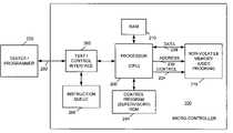
- Nonvolatile memory 216e.g., Flash memory
- a control path 224is provided from processor 206 to nonvolatile memory 216 .
- conventional address path 230 and data path 238 from processor 206 to memory 216is provided.
- microcontroller 200includes a control program ROM (a supervisor ROM) 244 that contains hard-coded instructions used by processor 206 to directly program memory locations of nonvolatile memory 216 .
- control program ROMa supervisor ROM
- a tester/programmer 220may be coupled to microcontroller 200 via a path 250 which, in the preferred embodiment, is a two wire bus carrying control, address and data information to an internal test/control interface 260 .
- the tester/programmer 220may be any suitable commercially available tester or programmer device that is or can be adapted to programming a programmable microcontroller. This includes those available from Cypress Microsystems (Bothell, Wash.).
- Cypress MicrosystemsBothell, Wash.
- any suitable computer or workstationthat is adapted to test or program a microcontroller can be considered a tester/controller 220 within the context of the present invention.
- the test/control interface 260is coupled to processor 206 to provide the processor with program instructions and other test and control function instructions from the tester/programmer 220 . Instructions from the tester/programmer 220 are stored in an instruction queue 268 for sequential retrieval and execution by processor 206 .
- test/control interface 250may invoke a programming operation using process 300 as depicted in FIG. 3 starting at an idle state of the microcontroller at 304 .
- Tester/programmer 220invokes the test/control mode (i.e., a supervisory mode) at 312 by issuing an appropriate control command to test/control interface 260 .
- a transfer phasebegins at 318 where transfers can be made to or from RAM or to the instruction queue 268 . Transfers can only be made during this transfer phase, thus providing a level of security against intruders since the actual programming of the non-volatile memory only occurs outside the transfer phase.
- microcontroller 200Once the microcontroller 200 is in the transfer phase, data to be written to the nonvolatile memory is transferred from the tester/programmer 220 to RAM memory 210 at 318 . Also during the transfer phase, instructions can be placed in the instruction queue 268 . In the present embodiment, all such transfers are bidirectional. Processor 206 continues to periodically inspect the instruction queue 268 to determine if an additional instruction is there for retrieval. If the queue is empty, control passes back to 318 to await the next transfer. If the queue is not empty at 326 , the next instruction is retrieved and executed at 330 by processor 206 from the instruction queue 268 .
- test and control instructionsmay be placed by in the queue whenever the test/control mode is invoked and those instructions are periodically retrieved and executed at 330 until the processor detects an instruction invoking the commencement of programming of nonvolatile memory 216 at 340 .
- processor 206detects the instruction invoking the programming mode at 340 , processor 206 begins executing a programming routine from a supervisory program stored in control program ROM 244 . If the program mode instruction is not a write instruction, control passes to 344 where the instruction is executed per the program stored in the supervisory ROM 244 and the instruction queue is checked to determine whether the instruction queue is empty at 326 .
- a memory to memory copyis then carried out at 350 to transfer the data in RAM memory 210 to nonvolatile memory 216 under control of processor 206 .
- the processormay invoke a test at 360 to determine that an accurate transfer has been carried out. This may be accomplished by a simple comparison of memory contents in RAM 210 with those in 216 or using any other process to assure the integrity of the transfer. In other embodiments, such a test may be omitted to enhance the speed of the transfer.
- the processreturns to 326 to retrieve the next instruction from the instruction queue (if present) at 318 .
- the test/controller interface 260 and the instruction queue 268are effectively disabled by virtue of not being in the transfer phase of 318 . This helps assure that the programming process is not disrupted or tampered with once initiated.
- microcontroller 200essentially isolates itself from the tester/programmer by disabling test/control interface 260 and instruction queue 268 (by virtue of leaving the transfer phase of 318 ) to minimize the possibility of an intruder attempting to tamper with the programming process.
- control process used to program the nonvolatile memory 216may be made completely independent of the tester/programmer since each individual microcontroller 200 includes hard-coded instructions for carrying out the programming in control program ROM 244 . Thus, the same tester/programmer might be used to control numerous microcontrollers having different internal processes for carrying out the programming.
- Process 400 of FIG. 4broadly describes this function starting at 304 where the microcontroller 200 is powered up and initialized as previously and enters the normal mode of operation at 308 .
- processor 206transfers into RAM 210 data that is or is intended to be programmed or written into the nonvolatile memory. That is, a snapshot of the information to be transferred to nonvolatile memory is placed in RAM 210 so that it can later be copied.
- the transfer at 404is carried out under the instructions stored in nonvolatile memory 216 forming a part of the user program. Also forming a part of the user program is an instruction to begin executing a programming operation on nonvolatile memory 216 at 408 .
- processor 206may invoke a reprogramming of the nonvolatile memory 216 itself without the need for the tester/programmer 220 .
- a memory to memory copy from RAM to nonvolatile memoryis carried out at 350 until the copy is complete.
- a testmay then be carried out for accuracy of the copy at 360 if desired after which the user program resumes operation in the normal operational mode at 412 and control returns to 308 .
- the present inventionprovides enhanced security by virtue of isolating not only the control lines, data lines and address lines of the nonvolatile memory from the tester/programmer but also isolates the tester/programmer from the actual process used to effect the programming or re-programming of the nonvolatile memory 216 .
- proprietary methods for invoking the actual programming of the nonvolatile memory 216may be securely retained within the secure environment of the microcontroller 200 itself without having to be revealed to the outside world in any way.
- the invention as describedprovides substantially enhanced security against intruders attempting to program or re-program the nonvolatile memory 216 .
- the above described inventionpermits the processor itself to reprogram the memory and thereby adapt in a manner heretofore unavailable in microcontrollers.
- the present inventionis preferably implemented using a programmed processor executing programming instructions that are broadly described above in flow chart form. Such instructions may be stored in any suitable electronic programming medium.
- Such instructionsmay be stored in any suitable electronic programming medium.
- those skilled in the artwill appreciate that the processes described above may be implemented in any number of variations and in many suitable programming languages without departing from the present invention. For example, the order of certain operations carried out can often be varied, and additional operations may be added without departing from the invention. Error trapping may be added and/or enhanced and variations may be made in user interface and information presentation without departing from the present invention. Such variations are contemplated and considered equivalent.
Landscapes
- Engineering & Computer Science (AREA)
- Software Systems (AREA)
- Theoretical Computer Science (AREA)
- General Engineering & Computer Science (AREA)
- Computer Security & Cryptography (AREA)
- Computer Hardware Design (AREA)
- Physics & Mathematics (AREA)
- General Physics & Mathematics (AREA)
- Microcomputers (AREA)
Abstract
Description
Claims (25)
Priority Applications (1)
| Application Number | Priority Date | Filing Date | Title |
|---|---|---|---|
| US09/875,599US7185162B1 (en) | 2000-10-26 | 2001-06-05 | Method and apparatus for programming a flash memory |
Applications Claiming Priority (2)
| Application Number | Priority Date | Filing Date | Title |
|---|---|---|---|
| US24370800P | 2000-10-26 | 2000-10-26 | |
| US09/875,599US7185162B1 (en) | 2000-10-26 | 2001-06-05 | Method and apparatus for programming a flash memory |
Publications (1)
| Publication Number | Publication Date |
|---|---|
| US7185162B1true US7185162B1 (en) | 2007-02-27 |
Family
ID=37769774
Family Applications (1)
| Application Number | Title | Priority Date | Filing Date |
|---|---|---|---|
| US09/875,599Expired - LifetimeUS7185162B1 (en) | 2000-10-26 | 2001-06-05 | Method and apparatus for programming a flash memory |
Country Status (1)
| Country | Link |
|---|---|
| US (1) | US7185162B1 (en) |
Cited By (52)
| Publication number | Priority date | Publication date | Assignee | Title |
|---|---|---|---|---|
| US20020108006A1 (en)* | 2000-10-26 | 2002-08-08 | Warren Snyder | Microcontroller programmable system on a chip |
| US20050102573A1 (en)* | 2003-11-03 | 2005-05-12 | Macronix International Co., Ltd. | In-circuit configuration architecture for embedded configurable logic array |
| US20060036973A1 (en)* | 2004-08-13 | 2006-02-16 | Kenneth Ogami | Method and an apparatus to design a processing system using a graphical user interface |
| US20060037007A1 (en)* | 2004-08-13 | 2006-02-16 | Warren Snyder | Providing hardware independence to automate code generation of processing device firmware |
| US20060259653A1 (en)* | 2003-12-23 | 2006-11-16 | Mueller Peter D | Using a processor to program a semiconductor memory |
| US20070273660A1 (en)* | 2006-05-26 | 2007-11-29 | Xiaoping Jiang | Multi-function slider in touchpad |
| US20070273659A1 (en)* | 2006-05-26 | 2007-11-29 | Xiaoping Jiang | Multi-function slider in touchpad |
| US20080258760A1 (en)* | 2007-04-17 | 2008-10-23 | Cypress Semiconductor Corporation | System level interconnect with programmable switching |
| US20080263334A1 (en)* | 2007-04-17 | 2008-10-23 | Cypress Semiconductor Corp. | Dynamically configurable and re-configurable data path |
| US7737724B2 (en) | 2007-04-17 | 2010-06-15 | Cypress Semiconductor Corporation | Universal digital block interconnection and channel routing |
| US7761845B1 (en) | 2002-09-09 | 2010-07-20 | Cypress Semiconductor Corporation | Method for parameterizing a user module |
| US7765095B1 (en) | 2000-10-26 | 2010-07-27 | Cypress Semiconductor Corporation | Conditional branching in an in-circuit emulation system |
| US7770113B1 (en) | 2001-11-19 | 2010-08-03 | Cypress Semiconductor Corporation | System and method for dynamically generating a configuration datasheet |
| US7774190B1 (en) | 2001-11-19 | 2010-08-10 | Cypress Semiconductor Corporation | Sleep and stall in an in-circuit emulation system |
| US7825688B1 (en) | 2000-10-26 | 2010-11-02 | Cypress Semiconductor Corporation | Programmable microcontroller architecture(mixed analog/digital) |
| US20100281145A1 (en)* | 2009-05-04 | 2010-11-04 | Cypress Semiconductor Corporation | Autonomous control in a programmable system |
| US7844437B1 (en) | 2001-11-19 | 2010-11-30 | Cypress Semiconductor Corporation | System and method for performing next placements and pruning of disallowed placements for programming an integrated circuit |
| US7893724B2 (en) | 2004-03-25 | 2011-02-22 | Cypress Semiconductor Corporation | Method and circuit for rapid alignment of signals |
| US20110219171A1 (en)* | 2010-03-05 | 2011-09-08 | 248 SolidState, Inc | Virtual channel support in a nonvolatile memory controller |
| US8042093B1 (en) | 2001-11-15 | 2011-10-18 | Cypress Semiconductor Corporation | System providing automatic source code generation for personalization and parameterization of user modules |
| US8040266B2 (en) | 2007-04-17 | 2011-10-18 | Cypress Semiconductor Corporation | Programmable sigma-delta analog-to-digital converter |
| US8049569B1 (en) | 2007-09-05 | 2011-11-01 | Cypress Semiconductor Corporation | Circuit and method for improving the accuracy of a crystal-less oscillator having dual-frequency modes |
| US8067948B2 (en) | 2006-03-27 | 2011-11-29 | Cypress Semiconductor Corporation | Input/output multiplexer bus |
| US8069428B1 (en) | 2001-10-24 | 2011-11-29 | Cypress Semiconductor Corporation | Techniques for generating microcontroller configuration information |
| US8069405B1 (en) | 2001-11-19 | 2011-11-29 | Cypress Semiconductor Corporation | User interface for efficiently browsing an electronic document using data-driven tabs |
| US8078894B1 (en) | 2007-04-25 | 2011-12-13 | Cypress Semiconductor Corporation | Power management architecture, method and configuration system |
| US8078970B1 (en) | 2001-11-09 | 2011-12-13 | Cypress Semiconductor Corporation | Graphical user interface with user-selectable list-box |
| US8085100B2 (en) | 2005-02-04 | 2011-12-27 | Cypress Semiconductor Corporation | Poly-phase frequency synthesis oscillator |
| US8085067B1 (en) | 2005-12-21 | 2011-12-27 | Cypress Semiconductor Corporation | Differential-to-single ended signal converter circuit and method |
| US8089461B2 (en) | 2005-06-23 | 2012-01-03 | Cypress Semiconductor Corporation | Touch wake for electronic devices |
| US8092083B2 (en) | 2007-04-17 | 2012-01-10 | Cypress Semiconductor Corporation | Temperature sensor with digital bandgap |
| US8103497B1 (en) | 2002-03-28 | 2012-01-24 | Cypress Semiconductor Corporation | External interface for event architecture |
| US8103496B1 (en) | 2000-10-26 | 2012-01-24 | Cypress Semicondutor Corporation | Breakpoint control in an in-circuit emulation system |
| US8120408B1 (en) | 2005-05-05 | 2012-02-21 | Cypress Semiconductor Corporation | Voltage controlled oscillator delay cell and method |
| US8130025B2 (en) | 2007-04-17 | 2012-03-06 | Cypress Semiconductor Corporation | Numerical band gap |
| US8149048B1 (en) | 2000-10-26 | 2012-04-03 | Cypress Semiconductor Corporation | Apparatus and method for programmable power management in a programmable analog circuit block |
| US8160864B1 (en) | 2000-10-26 | 2012-04-17 | Cypress Semiconductor Corporation | In-circuit emulator and pod synchronized boot |
| WO2012050934A3 (en)* | 2010-09-28 | 2012-06-21 | Fusion-Io, Inc. | Apparatus, system, and method for a direct interface between a memory controller and non-volatile memory using a command protocol |
| US8286125B2 (en) | 2004-08-13 | 2012-10-09 | Cypress Semiconductor Corporation | Model for a hardware device-independent method of defining embedded firmware for programmable systems |
| US8402313B1 (en) | 2002-05-01 | 2013-03-19 | Cypress Semiconductor Corporation | Reconfigurable testing system and method |
| US8499270B1 (en) | 2007-04-25 | 2013-07-30 | Cypress Semiconductor Corporation | Configuration of programmable IC design elements |
| US8516025B2 (en) | 2007-04-17 | 2013-08-20 | Cypress Semiconductor Corporation | Clock driven dynamic datapath chaining |
| US8527949B1 (en) | 2001-11-19 | 2013-09-03 | Cypress Semiconductor Corporation | Graphical user interface for dynamically reconfiguring a programmable device |
| US9047178B2 (en) | 2010-12-13 | 2015-06-02 | SanDisk Technologies, Inc. | Auto-commit memory synchronization |
| US9208071B2 (en) | 2010-12-13 | 2015-12-08 | SanDisk Technologies, Inc. | Apparatus, system, and method for accessing memory |
| US9218278B2 (en) | 2010-12-13 | 2015-12-22 | SanDisk Technologies, Inc. | Auto-commit memory |
| US9223662B2 (en) | 2010-12-13 | 2015-12-29 | SanDisk Technologies, Inc. | Preserving data of a volatile memory |
| US9305610B2 (en) | 2009-09-09 | 2016-04-05 | SanDisk Technologies, Inc. | Apparatus, system, and method for power reduction management in a storage device |
| US9720805B1 (en) | 2007-04-25 | 2017-08-01 | Cypress Semiconductor Corporation | System and method for controlling a target device |
| US10817421B2 (en) | 2010-12-13 | 2020-10-27 | Sandisk Technologies Llc | Persistent data structures |
| US10817502B2 (en) | 2010-12-13 | 2020-10-27 | Sandisk Technologies Llc | Persistent memory management |
| US11573909B2 (en) | 2006-12-06 | 2023-02-07 | Unification Technologies Llc | Apparatus, system, and method for managing commands of solid-state storage using bank interleave |
Citations (12)
| Publication number | Priority date | Publication date | Assignee | Title |
|---|---|---|---|---|
| US5202687A (en) | 1991-06-12 | 1993-04-13 | Intellectual Property Development Associates Of Connecticut | Analog to digital converter |
| US5630057A (en)* | 1988-06-14 | 1997-05-13 | Progressive Technology Inc. | Secure architecture and apparatus using an independent computer cartridge |
| US5969632A (en)* | 1996-11-22 | 1999-10-19 | Diamant; Erez | Information security method and apparatus |
| US6009496A (en)* | 1997-10-30 | 1999-12-28 | Winbond Electronics Corp. | Microcontroller with programmable embedded flash memory |
| US6144327A (en) | 1996-08-15 | 2000-11-07 | Intellectual Property Development Associates Of Connecticut, Inc. | Programmably interconnected programmable devices |
| US6219729B1 (en)* | 1998-03-31 | 2001-04-17 | Texas Instruments Incorporated | Apparatus and method for providing for efficient communication between high and low-level processing engine of a disk drive formatter |
| US6236593B1 (en)* | 1999-04-27 | 2001-05-22 | Samsung Electronics Co., Ltd. | Method for simultaneously programming plural flash memories having invalid blocks |
| US6324628B1 (en)* | 1999-08-24 | 2001-11-27 | Trimble Navigation Limited | Programming flash in a closed system |
| EP1191423A2 (en)* | 2000-09-25 | 2002-03-27 | Telesincro S.A. | Integrated circuit with cryptographic capabilities |
| US6460172B1 (en) | 1996-10-10 | 2002-10-01 | Semiconductors Investigacion Diseno, S.A. (Sidsa) | Microprocessor based mixed signal field programmable integrated device and prototyping methodology |
| US6754765B1 (en)* | 2001-05-14 | 2004-06-22 | Integrated Memory Logic, Inc. | Flash memory controller with updateable microcode |
| US6839774B1 (en)* | 1999-10-21 | 2005-01-04 | Samsung Electronics Co., Ltd. | Single-chip data processing apparatus incorporating an electrically rewritable nonvolatile memory and method of operating the same |
- 2001
- 2001-06-05USUS09/875,599patent/US7185162B1/ennot_activeExpired - Lifetime
Patent Citations (12)
| Publication number | Priority date | Publication date | Assignee | Title |
|---|---|---|---|---|
| US5630057A (en)* | 1988-06-14 | 1997-05-13 | Progressive Technology Inc. | Secure architecture and apparatus using an independent computer cartridge |
| US5202687A (en) | 1991-06-12 | 1993-04-13 | Intellectual Property Development Associates Of Connecticut | Analog to digital converter |
| US6144327A (en) | 1996-08-15 | 2000-11-07 | Intellectual Property Development Associates Of Connecticut, Inc. | Programmably interconnected programmable devices |
| US6460172B1 (en) | 1996-10-10 | 2002-10-01 | Semiconductors Investigacion Diseno, S.A. (Sidsa) | Microprocessor based mixed signal field programmable integrated device and prototyping methodology |
| US5969632A (en)* | 1996-11-22 | 1999-10-19 | Diamant; Erez | Information security method and apparatus |
| US6009496A (en)* | 1997-10-30 | 1999-12-28 | Winbond Electronics Corp. | Microcontroller with programmable embedded flash memory |
| US6219729B1 (en)* | 1998-03-31 | 2001-04-17 | Texas Instruments Incorporated | Apparatus and method for providing for efficient communication between high and low-level processing engine of a disk drive formatter |
| US6236593B1 (en)* | 1999-04-27 | 2001-05-22 | Samsung Electronics Co., Ltd. | Method for simultaneously programming plural flash memories having invalid blocks |
| US6324628B1 (en)* | 1999-08-24 | 2001-11-27 | Trimble Navigation Limited | Programming flash in a closed system |
| US6839774B1 (en)* | 1999-10-21 | 2005-01-04 | Samsung Electronics Co., Ltd. | Single-chip data processing apparatus incorporating an electrically rewritable nonvolatile memory and method of operating the same |
| EP1191423A2 (en)* | 2000-09-25 | 2002-03-27 | Telesincro S.A. | Integrated circuit with cryptographic capabilities |
| US6754765B1 (en)* | 2001-05-14 | 2004-06-22 | Integrated Memory Logic, Inc. | Flash memory controller with updateable microcode |
Non-Patent Citations (2)
| Title |
|---|
| CYPR-CD00232; "Programmable System on a Chip"; Oct. 10, 2001; U.S. Appl. No. 10/033,027; W. Snyder. |
| Hwang et al., Sep. 24, 2002, Derwent acc. No. 2002-758861.* |
Cited By (90)
| Publication number | Priority date | Publication date | Assignee | Title |
|---|---|---|---|---|
| US10725954B2 (en) | 2000-10-26 | 2020-07-28 | Monterey Research, Llc | Microcontroller programmable system on a chip |
| US8555032B2 (en) | 2000-10-26 | 2013-10-08 | Cypress Semiconductor Corporation | Microcontroller programmable system on a chip with programmable interconnect |
| US8736303B2 (en) | 2000-10-26 | 2014-05-27 | Cypress Semiconductor Corporation | PSOC architecture |
| US8358150B1 (en) | 2000-10-26 | 2013-01-22 | Cypress Semiconductor Corporation | Programmable microcontroller architecture(mixed analog/digital) |
| US9766650B2 (en) | 2000-10-26 | 2017-09-19 | Cypress Semiconductor Corporation | Microcontroller programmable system on a chip with programmable interconnect |
| US8176296B2 (en) | 2000-10-26 | 2012-05-08 | Cypress Semiconductor Corporation | Programmable microcontroller architecture |
| US8160864B1 (en) | 2000-10-26 | 2012-04-17 | Cypress Semiconductor Corporation | In-circuit emulator and pod synchronized boot |
| US8149048B1 (en) | 2000-10-26 | 2012-04-03 | Cypress Semiconductor Corporation | Apparatus and method for programmable power management in a programmable analog circuit block |
| US9843327B1 (en) | 2000-10-26 | 2017-12-12 | Cypress Semiconductor Corporation | PSOC architecture |
| US8103496B1 (en) | 2000-10-26 | 2012-01-24 | Cypress Semicondutor Corporation | Breakpoint control in an in-circuit emulation system |
| US10020810B2 (en) | 2000-10-26 | 2018-07-10 | Cypress Semiconductor Corporation | PSoC architecture |
| US10248604B2 (en) | 2000-10-26 | 2019-04-02 | Cypress Semiconductor Corporation | Microcontroller programmable system on a chip |
| US7765095B1 (en) | 2000-10-26 | 2010-07-27 | Cypress Semiconductor Corporation | Conditional branching in an in-circuit emulation system |
| US10261932B2 (en) | 2000-10-26 | 2019-04-16 | Cypress Semiconductor Corporation | Microcontroller programmable system on a chip |
| US20020108006A1 (en)* | 2000-10-26 | 2002-08-08 | Warren Snyder | Microcontroller programmable system on a chip |
| US7825688B1 (en) | 2000-10-26 | 2010-11-02 | Cypress Semiconductor Corporation | Programmable microcontroller architecture(mixed analog/digital) |
| US8069428B1 (en) | 2001-10-24 | 2011-11-29 | Cypress Semiconductor Corporation | Techniques for generating microcontroller configuration information |
| US8793635B1 (en) | 2001-10-24 | 2014-07-29 | Cypress Semiconductor Corporation | Techniques for generating microcontroller configuration information |
| US10466980B2 (en) | 2001-10-24 | 2019-11-05 | Cypress Semiconductor Corporation | Techniques for generating microcontroller configuration information |
| US8078970B1 (en) | 2001-11-09 | 2011-12-13 | Cypress Semiconductor Corporation | Graphical user interface with user-selectable list-box |
| US10698662B2 (en) | 2001-11-15 | 2020-06-30 | Cypress Semiconductor Corporation | System providing automatic source code generation for personalization and parameterization of user modules |
| US8042093B1 (en) | 2001-11-15 | 2011-10-18 | Cypress Semiconductor Corporation | System providing automatic source code generation for personalization and parameterization of user modules |
| US7774190B1 (en) | 2001-11-19 | 2010-08-10 | Cypress Semiconductor Corporation | Sleep and stall in an in-circuit emulation system |
| US8533677B1 (en) | 2001-11-19 | 2013-09-10 | Cypress Semiconductor Corporation | Graphical user interface for dynamically reconfiguring a programmable device |
| US7770113B1 (en) | 2001-11-19 | 2010-08-03 | Cypress Semiconductor Corporation | System and method for dynamically generating a configuration datasheet |
| US8527949B1 (en) | 2001-11-19 | 2013-09-03 | Cypress Semiconductor Corporation | Graphical user interface for dynamically reconfiguring a programmable device |
| US7844437B1 (en) | 2001-11-19 | 2010-11-30 | Cypress Semiconductor Corporation | System and method for performing next placements and pruning of disallowed placements for programming an integrated circuit |
| US8370791B2 (en) | 2001-11-19 | 2013-02-05 | Cypress Semiconductor Corporation | System and method for performing next placements and pruning of disallowed placements for programming an integrated circuit |
| US8069405B1 (en) | 2001-11-19 | 2011-11-29 | Cypress Semiconductor Corporation | User interface for efficiently browsing an electronic document using data-driven tabs |
| US8103497B1 (en) | 2002-03-28 | 2012-01-24 | Cypress Semiconductor Corporation | External interface for event architecture |
| US8402313B1 (en) | 2002-05-01 | 2013-03-19 | Cypress Semiconductor Corporation | Reconfigurable testing system and method |
| US7761845B1 (en) | 2002-09-09 | 2010-07-20 | Cypress Semiconductor Corporation | Method for parameterizing a user module |
| US20050102573A1 (en)* | 2003-11-03 | 2005-05-12 | Macronix International Co., Ltd. | In-circuit configuration architecture for embedded configurable logic array |
| US7594065B2 (en)* | 2003-12-23 | 2009-09-22 | Marvell International Ltd. | Using a processor to program a semiconductor memory |
| US20060259653A1 (en)* | 2003-12-23 | 2006-11-16 | Mueller Peter D | Using a processor to program a semiconductor memory |
| US7893724B2 (en) | 2004-03-25 | 2011-02-22 | Cypress Semiconductor Corporation | Method and circuit for rapid alignment of signals |
| US8082531B2 (en) | 2004-08-13 | 2011-12-20 | Cypress Semiconductor Corporation | Method and an apparatus to design a processing system using a graphical user interface |
| US8539398B2 (en) | 2004-08-13 | 2013-09-17 | Cypress Semiconductor Corporation | Model for a hardware device-independent method of defining embedded firmware for programmable systems |
| US20060036973A1 (en)* | 2004-08-13 | 2006-02-16 | Kenneth Ogami | Method and an apparatus to design a processing system using a graphical user interface |
| US8069436B2 (en) | 2004-08-13 | 2011-11-29 | Cypress Semiconductor Corporation | Providing hardware independence to automate code generation of processing device firmware |
| US20060037007A1 (en)* | 2004-08-13 | 2006-02-16 | Warren Snyder | Providing hardware independence to automate code generation of processing device firmware |
| US8286125B2 (en) | 2004-08-13 | 2012-10-09 | Cypress Semiconductor Corporation | Model for a hardware device-independent method of defining embedded firmware for programmable systems |
| US8085100B2 (en) | 2005-02-04 | 2011-12-27 | Cypress Semiconductor Corporation | Poly-phase frequency synthesis oscillator |
| US8120408B1 (en) | 2005-05-05 | 2012-02-21 | Cypress Semiconductor Corporation | Voltage controlled oscillator delay cell and method |
| US8089461B2 (en) | 2005-06-23 | 2012-01-03 | Cypress Semiconductor Corporation | Touch wake for electronic devices |
| US8085067B1 (en) | 2005-12-21 | 2011-12-27 | Cypress Semiconductor Corporation | Differential-to-single ended signal converter circuit and method |
| US8067948B2 (en) | 2006-03-27 | 2011-11-29 | Cypress Semiconductor Corporation | Input/output multiplexer bus |
| US8717042B1 (en) | 2006-03-27 | 2014-05-06 | Cypress Semiconductor Corporation | Input/output multiplexer bus |
| US20070273660A1 (en)* | 2006-05-26 | 2007-11-29 | Xiaoping Jiang | Multi-function slider in touchpad |
| US20070273659A1 (en)* | 2006-05-26 | 2007-11-29 | Xiaoping Jiang | Multi-function slider in touchpad |
| US8089472B2 (en) | 2006-05-26 | 2012-01-03 | Cypress Semiconductor Corporation | Bidirectional slider with delete function |
| US8537121B2 (en) | 2006-05-26 | 2013-09-17 | Cypress Semiconductor Corporation | Multi-function slider in touchpad |
| US11960412B2 (en) | 2006-12-06 | 2024-04-16 | Unification Technologies Llc | Systems and methods for identifying storage resources that are not in use |
| US11847066B2 (en) | 2006-12-06 | 2023-12-19 | Unification Technologies Llc | Apparatus, system, and method for managing commands of solid-state storage using bank interleave |
| US11640359B2 (en) | 2006-12-06 | 2023-05-02 | Unification Technologies Llc | Systems and methods for identifying storage resources that are not in use |
| US11573909B2 (en) | 2006-12-06 | 2023-02-07 | Unification Technologies Llc | Apparatus, system, and method for managing commands of solid-state storage using bank interleave |
| US8026739B2 (en) | 2007-04-17 | 2011-09-27 | Cypress Semiconductor Corporation | System level interconnect with programmable switching |
| US9564902B2 (en) | 2007-04-17 | 2017-02-07 | Cypress Semiconductor Corporation | Dynamically configurable and re-configurable data path |
| US20080258760A1 (en)* | 2007-04-17 | 2008-10-23 | Cypress Semiconductor Corporation | System level interconnect with programmable switching |
| US20080263334A1 (en)* | 2007-04-17 | 2008-10-23 | Cypress Semiconductor Corp. | Dynamically configurable and re-configurable data path |
| US7737724B2 (en) | 2007-04-17 | 2010-06-15 | Cypress Semiconductor Corporation | Universal digital block interconnection and channel routing |
| US8476928B1 (en) | 2007-04-17 | 2013-07-02 | Cypress Semiconductor Corporation | System level interconnect with programmable switching |
| US8040266B2 (en) | 2007-04-17 | 2011-10-18 | Cypress Semiconductor Corporation | Programmable sigma-delta analog-to-digital converter |
| US8092083B2 (en) | 2007-04-17 | 2012-01-10 | Cypress Semiconductor Corporation | Temperature sensor with digital bandgap |
| US8130025B2 (en) | 2007-04-17 | 2012-03-06 | Cypress Semiconductor Corporation | Numerical band gap |
| US8516025B2 (en) | 2007-04-17 | 2013-08-20 | Cypress Semiconductor Corporation | Clock driven dynamic datapath chaining |
| US9720805B1 (en) | 2007-04-25 | 2017-08-01 | Cypress Semiconductor Corporation | System and method for controlling a target device |
| US8909960B1 (en) | 2007-04-25 | 2014-12-09 | Cypress Semiconductor Corporation | Power management architecture, method and configuration system |
| US8499270B1 (en) | 2007-04-25 | 2013-07-30 | Cypress Semiconductor Corporation | Configuration of programmable IC design elements |
| US8078894B1 (en) | 2007-04-25 | 2011-12-13 | Cypress Semiconductor Corporation | Power management architecture, method and configuration system |
| US8049569B1 (en) | 2007-09-05 | 2011-11-01 | Cypress Semiconductor Corporation | Circuit and method for improving the accuracy of a crystal-less oscillator having dual-frequency modes |
| US9448964B2 (en) | 2009-05-04 | 2016-09-20 | Cypress Semiconductor Corporation | Autonomous control in a programmable system |
| US20100281145A1 (en)* | 2009-05-04 | 2010-11-04 | Cypress Semiconductor Corporation | Autonomous control in a programmable system |
| US9305610B2 (en) | 2009-09-09 | 2016-04-05 | SanDisk Technologies, Inc. | Apparatus, system, and method for power reduction management in a storage device |
| CN102193885B (en)* | 2010-03-05 | 2014-04-23 | 晶先锋科技有限公司 | Non-volatile memory controller with virtual channel support |
| US20110219171A1 (en)* | 2010-03-05 | 2011-09-08 | 248 SolidState, Inc | Virtual channel support in a nonvolatile memory controller |
| CN102193885A (en)* | 2010-03-05 | 2011-09-21 | 248固态硬碟有限公司 | Virtual channel support in a nonvolatile memory controller |
| US8310880B2 (en)* | 2010-03-05 | 2012-11-13 | 248 Solid State, Inc. | Virtual channel support in a nonvolatile memory controller |
| US9575882B2 (en) | 2010-09-28 | 2017-02-21 | Sandisk Technologies Llc | Non-volatile memory interface |
| WO2012050934A3 (en)* | 2010-09-28 | 2012-06-21 | Fusion-Io, Inc. | Apparatus, system, and method for a direct interface between a memory controller and non-volatile memory using a command protocol |
| US9159419B2 (en) | 2010-09-28 | 2015-10-13 | Intelligent Intellectual Property Holdings 2 Llc | Non-volatile memory interface |
| US8688899B2 (en) | 2010-09-28 | 2014-04-01 | Fusion-Io, Inc. | Apparatus, system, and method for an interface between a memory controller and a non-volatile memory controller using a command protocol |
| US9047178B2 (en) | 2010-12-13 | 2015-06-02 | SanDisk Technologies, Inc. | Auto-commit memory synchronization |
| US9772938B2 (en) | 2010-12-13 | 2017-09-26 | Sandisk Technologies Llc | Auto-commit memory metadata and resetting the metadata by writing to special address in free space of page storing the metadata |
| US9767017B2 (en) | 2010-12-13 | 2017-09-19 | Sandisk Technologies Llc | Memory device with volatile and non-volatile media |
| US10817421B2 (en) | 2010-12-13 | 2020-10-27 | Sandisk Technologies Llc | Persistent data structures |
| US10817502B2 (en) | 2010-12-13 | 2020-10-27 | Sandisk Technologies Llc | Persistent memory management |
| US9218278B2 (en) | 2010-12-13 | 2015-12-22 | SanDisk Technologies, Inc. | Auto-commit memory |
| US9208071B2 (en) | 2010-12-13 | 2015-12-08 | SanDisk Technologies, Inc. | Apparatus, system, and method for accessing memory |
| US9223662B2 (en) | 2010-12-13 | 2015-12-29 | SanDisk Technologies, Inc. | Preserving data of a volatile memory |
Similar Documents
| Publication | Publication Date | Title |
|---|---|---|
| US7185162B1 (en) | Method and apparatus for programming a flash memory | |
| US5495593A (en) | Microcontroller device having remotely programmable EPROM and method for programming | |
| US7131114B2 (en) | Debugger breakpoint management in a multicore DSP device having shared program memory | |
| JP2682700B2 (en) | IC card | |
| US7039779B2 (en) | Access monitor and access monitoring method for monitoring access between programs | |
| EP3242199B1 (en) | Flash memory controller and control method for flash memory controller | |
| KR970012145A (en) | How to work with the data processor, how to run its debugging operations, and how to modify its breakpoint values | |
| JP2001256460A (en) | One-chip microcomputer and IC card using the same | |
| JPH07504282A (en) | Microcontroller power-up delay device | |
| EP3242214B1 (en) | Method and device for protecting information of mcu chip | |
| KR20030059339A (en) | Single-step processing | |
| US5721877A (en) | Method and apparatus for limiting access to nonvolatile memory device | |
| US20070136565A1 (en) | Stack underflow debug with sticky base | |
| CN101639877A (en) | Electronic device and method for updating basic input and output system thereof | |
| US11675587B2 (en) | Enhanced protection of processors from a buffer overflow attack | |
| US20080005799A1 (en) | Program execution control circuit, computer system, and IC card | |
| US5930470A (en) | Debugging system and debugging method | |
| CN1251183A (en) | Integrated circuit and method for testing the same | |
| US4985826A (en) | Method and device to execute two instruction sequences in an order determined in advance | |
| US5657444A (en) | Microprocessor with secure programmable read only memory circuit | |
| US5592650A (en) | Computer apparatus and method for replacing programs between memories by employing protection mechanism with write enable generation scheme | |
| US6742073B1 (en) | Bus controller technique to control N buses | |
| US7082522B2 (en) | Method and/or apparatus for implementing enhanced device identification | |
| JP2638078B2 (en) | Information processing device | |
| US20030145195A1 (en) | BIOS call technique for operating system device driver |
Legal Events
| Date | Code | Title | Description |
|---|---|---|---|
| AS | Assignment | Owner name:CYPRESS SEMICONDUCTOR CORPORATION, CALIFORNIA Free format text:ASSIGNMENT OF ASSIGNORS INTEREST;ASSIGNOR:SNYDER, WARREN;REEL/FRAME:011900/0705 Effective date:20010531 | |
| STCF | Information on status: patent grant | Free format text:PATENTED CASE | |
| FEPP | Fee payment procedure | Free format text:PAYER NUMBER DE-ASSIGNED (ORIGINAL EVENT CODE: RMPN); ENTITY STATUS OF PATENT OWNER: LARGE ENTITY Free format text:PAYOR NUMBER ASSIGNED (ORIGINAL EVENT CODE: ASPN); ENTITY STATUS OF PATENT OWNER: LARGE ENTITY | |
| FPAY | Fee payment | Year of fee payment:4 | |
| FPAY | Fee payment | Year of fee payment:8 | |
| AS | Assignment | Owner name:MORGAN STANLEY SENIOR FUNDING, INC., NEW YORK Free format text:SECURITY INTEREST;ASSIGNORS:CYPRESS SEMICONDUCTOR CORPORATION;SPANSION LLC;REEL/FRAME:035240/0429 Effective date:20150312 | |
| MAFP | Maintenance fee payment | Free format text:PAYMENT OF MAINTENANCE FEE, 12TH YEAR, LARGE ENTITY (ORIGINAL EVENT CODE: M1553); ENTITY STATUS OF PATENT OWNER: LARGE ENTITY Year of fee payment:12 | |
| AS | Assignment | Owner name:MUFG UNION BANK, N.A., CALIFORNIA Free format text:ASSIGNMENT AND ASSUMPTION OF SECURITY INTEREST IN INTELLECTUAL PROPERTY;ASSIGNOR:MORGAN STANLEY SENIOR FUNDING, INC.;REEL/FRAME:050896/0366 Effective date:20190731 | |
| AS | Assignment | Owner name:MORGAN STANLEY SENIOR FUNDING, INC., NEW YORK Free format text:CORRECTIVE ASSIGNMENT TO CORRECT THE 8647899 PREVIOUSLY RECORDED ON REEL 035240 FRAME 0429. ASSIGNOR(S) HEREBY CONFIRMS THE SECURITY INTERST;ASSIGNORS:CYPRESS SEMICONDUCTOR CORPORATION;SPANSION LLC;REEL/FRAME:058002/0470 Effective date:20150312 | |
| AS | Assignment | Owner name:SPANSION LLC, CALIFORNIA Free format text:RELEASE BY SECURED PARTY;ASSIGNOR:MUFG UNION BANK, N.A.;REEL/FRAME:059410/0438 Effective date:20200416 Owner name:CYPRESS SEMICONDUCTOR CORPORATION, CALIFORNIA Free format text:RELEASE BY SECURED PARTY;ASSIGNOR:MUFG UNION BANK, N.A.;REEL/FRAME:059410/0438 Effective date:20200416 |