US7184319B2 - Method for erasing non-volatile memory cells and corresponding memory device - Google Patents
Method for erasing non-volatile memory cells and corresponding memory deviceDownload PDFInfo
- Publication number
- US7184319B2 US7184319B2US10/675,221US67522103AUS7184319B2US 7184319 B2US7184319 B2US 7184319B2US 67522103 AUS67522103 AUS 67522103AUS 7184319 B2US7184319 B2US 7184319B2
- Authority
- US
- United States
- Prior art keywords
- row
- sector
- failed
- decode
- block
- Prior art date
- Legal status (The legal status is an assumption and is not a legal conclusion. Google has not performed a legal analysis and makes no representation as to the accuracy of the status listed.)
- Expired - Lifetime
Links
Images


Classifications
- G—PHYSICS
- G11—INFORMATION STORAGE
- G11C—STATIC STORES
- G11C29/00—Checking stores for correct operation ; Subsequent repair; Testing stores during standby or offline operation
- G11C29/70—Masking faults in memories by using spares or by reconfiguring
- G11C29/78—Masking faults in memories by using spares or by reconfiguring using programmable devices
- G11C29/80—Masking faults in memories by using spares or by reconfiguring using programmable devices with improved layout
- G11C29/816—Masking faults in memories by using spares or by reconfiguring using programmable devices with improved layout for an application-specific layout
- G11C29/82—Masking faults in memories by using spares or by reconfiguring using programmable devices with improved layout for an application-specific layout for EEPROMs
- G—PHYSICS
- G11—INFORMATION STORAGE
- G11C—STATIC STORES
- G11C16/00—Erasable programmable read-only memories
- G11C16/02—Erasable programmable read-only memories electrically programmable
- G11C16/06—Auxiliary circuits, e.g. for writing into memory
- G11C16/10—Programming or data input circuits
- G11C16/14—Circuits for erasing electrically, e.g. erase voltage switching circuits
- G11C16/16—Circuits for erasing electrically, e.g. erase voltage switching circuits for erasing blocks, e.g. arrays, words, groups
- G—PHYSICS
- G11—INFORMATION STORAGE
- G11C—STATIC STORES
- G11C29/00—Checking stores for correct operation ; Subsequent repair; Testing stores during standby or offline operation
- G11C29/04—Detection or location of defective memory elements, e.g. cell constructio details, timing of test signals
- G11C29/08—Functional testing, e.g. testing during refresh, power-on self testing [POST] or distributed testing
- G11C29/12—Built-in arrangements for testing, e.g. built-in self testing [BIST] or interconnection details
- G11C29/44—Indication or identification of errors, e.g. for repair
- G—PHYSICS
- G11—INFORMATION STORAGE
- G11C—STATIC STORES
- G11C16/00—Erasable programmable read-only memories
- G11C16/02—Erasable programmable read-only memories electrically programmable
- G11C16/04—Erasable programmable read-only memories electrically programmable using variable threshold transistors, e.g. FAMOS
- G—PHYSICS
- G11—INFORMATION STORAGE
- G11C—STATIC STORES
- G11C29/00—Checking stores for correct operation ; Subsequent repair; Testing stores during standby or offline operation
- G11C29/04—Detection or location of defective memory elements, e.g. cell constructio details, timing of test signals
- G11C29/08—Functional testing, e.g. testing during refresh, power-on self testing [POST] or distributed testing
- G11C29/12—Built-in arrangements for testing, e.g. built-in self testing [BIST] or interconnection details
- G11C2029/1208—Error catch memory
Definitions
- the present inventionrelates to a method for erasing non-volatile memory cells incorporated in a memory cell array divided into sectors.
- This faulty conditionis determined by the way an erase operation, the so-called channel erasing, is carried out.
- FIG. 1shows, schematically and to an enlarged scale, a portion of a semiconductor integrated circuit, which is fabricated conventionally to a flash memory cell 4 .
- this portion 1comprises a substrate 2 doped with a first dopant that may be of the P type.
- the substrate 2serves the whole wafer where the portion 1 is also formed.
- a three-well structureincluding an intermediate well 3 and an innermost well 5 in which the flash memory cell 4 is integrated, is preferably formed in the substrate 2 .
- all the cells 4 of a given sector of the flash memory arrayare formed in the innermost well 5 .
- the well 5is also doped with the first dopant of the P type, and a source region 6 and a drain region 7 of the cell 4 are formed towards its surface. These regions are islands of a second type of dopants that may be of the N type.
- a thin layer of tunnel oxideseparates the surface of the well 5 from a floating gate region 8 , the latter being separated from a control gate region 9 by means of an isolation layer 10 , which is usually an interpoly oxide 10 , also called ONO layer.
- the cell 4is connected to first or positive and second or negative charge pump circuits 11 and 12 , respectively.
- the innermost well 5is applied a predetermined positive voltage value by means of the first or positive charge pump circuit 11 .
- the value of this positive voltageusually reaches +8V, and is also applied to the floating gate region 8 .
- the control gate region 9is brought to a negative voltage value that reaches ⁇ 9V by means of the second charge pump circuit 12 .
- FIG. 1this situation is schematically shown, in the form of paths illustrating the application of the above voltage values.
- the voltage across the interpoly oxide layer 10may rise to a value equal to 17V and exceed it.
- the layeris apt to deteriorate and even to break.
- the second or negative charge pump circuit 12becomes shorted to the first or positive charge pump circuit 11 while the cell 4 is erased, as indicated in FIG. 2 by the conduction path 13 .
- a net outcomeis that one or more of the cells in the sector affected by the short-circuit in well 5 is not erased, thus bringing the memory to an erase-fail state.
- the prior artalready proposes a way to overcome this problem that consists of applying a field redundancy concept in the erase algorithm, with attendant sector redundancy.
- this prior proposalconsists of replacing a failed memory element, or even a whole memory sector, with a new element.
- the erase algorithmis suitably modified, so to have the erase operation performed on the redundant sectors and not on the failed sectors anymore.
- redundancy operationwould be available through the service life of a memory device on the market, as well as to the test procedures for factory testing memory devices before delivery.
- a check phaseis performed, which allows to divert the erase operation to a “sparing” sector in the event of sector failing and thus to properly erase such a sector.
- the underlying technical objective of this inventionis to provide a method of erasing non-volatile memory cells, and a memory device implementing the method, with appropriate functional and constructional features.
- the solution on which the present invention standsincludes pinpointing the elements responsible for a fail condition and suitably isolating them from the remainder of the sector, such that only these elements will become involved in the redundancy procedure.
- the inventionprovides a redundancy feature aimed at each sector rather than at the whole device.
- the inventionrelates to a method of erasing non-volatile memory cells in an integrated non-volatile memory device that comprises a memory cell array organized in a row-and-column layout and divided in array sectors, each including at least one row decode circuit portion being supplied positive and negative voltages, and of the type wherein the array sectors can be erased independently of one another by means of an erase algorithm.
- the inventionalso relates to an integrated memory device implementing the above method.
- the inventionrelates to an electronic memory device, which is monolithically integrated in a semiconductor and comprises an array of non-volatile memory cells, e.g., flash EEPROM cells; the following description is made with reference to the above application field for convenience of illustration only.
- non-volatile memory cellse.g., flash EEPROM cells
- FIG. 1schematically shows a portion of a semiconductor substrate where a non-volatile memory cell has been integrated according to the prior art.
- FIG. 2schematically shows the same cell as in FIG. 1 and the fail condition, the so called erasing fail.
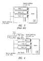
- FIG. 3schematically shows the row decode arrangement in an integrated non-volatile memory device according to the prior art.
- FIG. 4schematically shows a detail of the row decode arrangement in an integrated non-volatile memory device according to the invention.
- FIG. 5schematically shows another detail of a row decode arrangement according to the invention.
- FIG. 6shows a detailed view of the memory device according to the invention, shown at one stage of its operation.
- FIG. 7shows a detailed view of the memory device according to the invention, shown at another stage of its operation.
- FIG. 8schematically shows an embodiment of a row decode arrangement according to the invention.
- FIG. 9shows a detailed view of the memory device according to the invention, shown at said another stage of its operation, but with an indication of parasitic capacitance.
- FIG. 10shows a general view of the row decode embodiment shown in FIG. 8 .
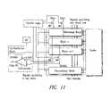
- FIG. 11schematically shows a structurally detailed view of the row decode embodiment shown in FIG. 8 .
- FIG. 12is a flow chart showing the main operations performed by the memory cell erasing method according to the invention.
- An erase fail conditionis caused by the negative charge pump circuit 12 , arranged to energize the control gate region (hereinafter abbreviated to “gate region”) of a failed memory cell 4 , becoming shorted to the positive charge pump circuit 11 which is energizing the source region 6 of the cell and the common substrate 5 of all the cells in a sector.
- gate regionthe control gate region
- the voltage used during erase operationscan be maintained not even if the failure occurs just at one cell.
- the voltage valuesare those provided by the splitting effect caused by the short-circuit and are transferred to both the control gate regions of the cells in the same row as the failed cell and to the gate regions of the other cells in the same sector.
- theseare insufficient voltages to produce the electric fields that are required in order to start the tunneling effect which would enable the erase operation to be performed.
- this inventionadvantageously provides for redundant rows to be borne inside the memory device sector where a fail is likely to occur.
- Memory devicemeans here any monolithic electronic device that comprises an array of memory cells, laid into rows and columns, and circuit portions that are associated with the cell array to serve the functions of addressing, decoding, reading, writing, and erasing the contents of memory cells.
- Such a devicemay be a sectored, electrically erasable non-volatile flash EEPROM chip integrated in a semiconductor.
- Each memory cellswould comprise a floating gate transistor having source, drain, and control gate terminals.
- the circuit portions that are associated with the cell arrayinclude a row decode circuit portion, which is associated with each of the sectors and supplied by specified positive and negative voltages, being generated within the integrated memory circuit by voltage boosters or charge pumps and regulated by respective voltage regulators.
- the teachings of this inventionapply to an integrated memory device, wherein the array sectors can be erased independently of one another by means of an erase algorithm.
- the inventioncan correct a fail condition of even a single cell in one sector, by providing a local redundancy for each sector.
- the invention“suppresses” the spurious current caused by a failed cell that would also harm intact cells in the same sector.
- the contribution from said spurious currentis cancelled by a modified row decode structure provided within the non-volatile memory device.
- the row decode featureis obtained by having a basic decode block, associated with a memory cell array sector, replicated n times; some addresses will enable a given block, and others will enable a row within the given selected block.
- This pre-encoding and decoding procedureallows a huge number of rows to be addressed by using a few signals. This structural scheme is illustrated in FIG. 3 .
- the inventionemploys at least one switch placed between the power supply and the decode blocks, as shown in FIG. 4 .
- first switch M 1 and a second switch M 2are shown in FIG. 4 , which are connected between the positive supply Vpcx and the first two of the decode blocks, a separate switch between the power supply and each decode block would be preferable.
- the positive supply Vpcx for reading and programmingcan be disconnected from a row block, in particular a row block that contains a failed cell.
- Control logic 15is arranged to control the transistor switches.
- the logic 15is operatively interlinked with the contents of redundancy registers.
- the redundancy registersstore the addresses of the failed rows and thus this information is provided to the control logic as to which rows to disconnect from the power supply.
- This solutiondoes not totally solve the erase problem, but it allows a row block containing a failed cell to be pinpointed during read and program operations.
- a switchcould be also provided in the conduction path from the negative voltage to the array rows, while still going through the row decode.
- thisis an NMOS transistor as customarily provided in the final stage of a so-called row driver.
- FIG. 5Shown in FIG. 5 is an embodiment of the above arrangement where a switch M 3 in block n and a switch M 4 in block (n+1) are provided.
- switchescan be made with different constructions, simple MOS transistors, specifically NMOS transistors, are preferred.
- the switches M 3 , M 4are inserted in a conduction path through which the first and second decode blocks can be applied a negative voltage HVNEG for the purpose of cutting off the row block that contains a failed cell each time that the sector where the failed cell locates is addressed. These switches M 3 , M 4 are controlled by the logic 15 interlinked to the redundancy registers.
- the switches provided, M 3 or M 4allow a row associated with a given sector to be set to float during operations that make use of the source and gate terminals of a given cell.
- FIG. 6shows in greater detail the general circuit layout that would be called to work in an erase operation.
- One sector 20is shown there for simplicity, which contains four cells 4 located in two rows 21 , 22 , and associated final drivers 23 , 24 of the same rows.
- Transistors M 1 and M 2are switches connected between the positive supply voltage Vpcx, which voltage would be taken to a row of memory array sector 20 during cell read and program operations.
- Transistors M 3 and M 4are switches connected between the negative voltage supply HVNEG, this voltage being taken to the same row of the array sector 20 during an erase operation. The row is applied ground voltage during the read and program operations.
- FIG. 6also shows a VPD positive charge pump 26 arranged to take a positive voltage to the source and substrate regions 6 and 5 of the cell 4 .
- the substrate and source voltages of the cell 4can be made unrelated to each other since, during the program operation, the body region can be brought to a negative potential, while the source is held to ground. This increases programming efficiency.
- An enable transistor M 5is connected in a conduction path that connects the pump 26 to the source regions 6 , and an enable transistor M 7 is inserted in a conduction path that connects the pump 26 to the body regions.
- the possible negative voltageis supplied over another conduction path that includes an enable transistor M 9 , as shown in FIG. 6 .
- a negative voltage charge pump 27is specifically provided for the body regions.
- a discharge pathis activated between the positive supply pump Vpcx to the gates and the substrate 5 , as shown in FIG. 7 .
- the row that contains a failed celle.g., row 24
- the row that contains a failed cellis placed into a floating state.
- Thisis achieved by driving the switches M 1 , M 2 by means of the redundancy register signals that are associated with the positive supply VPCX, as well as the switches M 3 , M 4 that are associated with the negative supply HVNEG and belonging to blocks of rows placed inside one sector.
- the corresponding switches of a redundant row block provided inside one sector 20 and associated with a respective decode block 28as shown in FIG. 8 , are enabled.
- the faulty rowmust be first singled out. This complication is the price to be paid in order to have only one part of the sector replaced.
- a spurious currentcan be detected across the gate and body terminals of the failed cell. This spurious current would not be present in the memory device under normal conditions; in fact, the node of the array row is a purely capacitive node with no currents to other points when the row contains only sound cells (actually, each row exhibits a resistance of a few kiloOhms).
- the failed cellor merely the failed row, can be recognized by detecting this current.
- a preferred procedureis that of using the memory device to force the sector that has not been fully erased into a read state; in this way the sector rows are scanned and the path shown in FIGS. 7 and 9 checked for the presence of a current through it.
- parasitic capacitancesare itemized here below as:
- a compare block 30shown in FIG. 10 , picks up the voltage at node B, this being the voltage at the row start, and monitors its rise curve. If a spurious current exists the row will tend to rise, thus revealing the presence of the spurious current.
- the compare block 30is input a reference signal Vrif from a redundant row or dummy row, known to be operative. This signal is obtained simply by duplicating the affected path with a set of rows that is never erased and never could have potentials such to originate the fault.
- block 30The inner structure of block 30 is shown in detail in FIG. 11 .
- This blockincludes a comparator and illustrates the general architecture for row decoding of this invention.
- the flow chart of FIG. 12schematically shows the main steps of the erasing method of this invention.
- the read algorithmis started in order to scan the row blocks in the estimated failed sector. Concurrently therewith, each time that a row block is addressed, a dummy row block will also be addressed, and after a time T of about a few tens nanoseconds (the time required for the row to become charged), a comparison of the two nodes in block 30 can be performed.
- the node of the redundancy dummy rowwill be the same value as the supply Vpcx, but the node of the addressed row in the addressed block 20 is bound to be a different value because of the spurious current.
- One or more redundant rowsare provided close to the rows in the sector, preferably within each sector in one embodiment, or in a location adjacent to the sector, within a threshold distance, so they can easily be provided to replace a row in a sector.
- the searchis maintained to the sector end.
- the position of the redundancy flagtells whether the operation has been successful.
Landscapes
- For Increasing The Reliability Of Semiconductor Memories (AREA)
- Read Only Memory (AREA)
Abstract
Description
- Crow, a row capacitance on the order of a picoFarad;
- Cvpcx, the capacitance of a whole row decode, on the order of 100 pF;
- Cbloc, the capacitance of a row block; if each block has eight rows, for example, this capacitance may amount to 1 pF;
Claims (22)
Applications Claiming Priority (2)
| Application Number | Priority Date | Filing Date | Title |
|---|---|---|---|
| EP02425591.1 | 2002-09-30 | ||
| EP02425591AEP1403879B1 (en) | 2002-09-30 | 2002-09-30 | Method for replacing failed non-volatile memory cells and corresponding memory device |
Publications (2)
| Publication Number | Publication Date |
|---|---|
| US20040208063A1 US20040208063A1 (en) | 2004-10-21 |
| US7184319B2true US7184319B2 (en) | 2007-02-27 |
Family
ID=31970526
Family Applications (1)
| Application Number | Title | Priority Date | Filing Date |
|---|---|---|---|
| US10/675,221Expired - LifetimeUS7184319B2 (en) | 2002-09-30 | 2003-09-30 | Method for erasing non-volatile memory cells and corresponding memory device |
Country Status (3)
| Country | Link |
|---|---|
| US (1) | US7184319B2 (en) |
| EP (1) | EP1403879B1 (en) |
| DE (1) | DE60238192D1 (en) |
Cited By (1)
| Publication number | Priority date | Publication date | Assignee | Title |
|---|---|---|---|---|
| US20100199150A1 (en)* | 2007-10-19 | 2010-08-05 | Anobit Technologies Ltd | Data Storage In Analog Memory Cell Arrays Having Erase Failures |
Families Citing this family (2)
| Publication number | Priority date | Publication date | Assignee | Title |
|---|---|---|---|---|
| US7512015B1 (en)* | 2006-07-17 | 2009-03-31 | Lattice Semiconductor Corporation | Negative voltage blocking for embedded memories |
| CN108418589B (en)* | 2018-03-05 | 2020-07-10 | 华中科技大学 | Dynamic coding and decoding method for single-layer nonvolatile memory |
Citations (19)
| Publication number | Priority date | Publication date | Assignee | Title |
|---|---|---|---|---|
| US4538245A (en)* | 1982-04-12 | 1985-08-27 | Seeq Technology, Inc. | Enabling circuit for redundant word lines in a semiconductor memory array |
| US5077691A (en) | 1989-10-23 | 1991-12-31 | Advanced Micro Devices, Inc. | Flash EEPROM array with negative gate voltage erase operation |
| US5233559A (en)* | 1991-02-11 | 1993-08-03 | Intel Corporation | Row redundancy for flash memories |
| US5262993A (en)* | 1990-11-16 | 1993-11-16 | Hitachi, Ltd. | Semiconductor memory having redundancy circuit with means to switch power from a normal memory block to a spare memory block |
| US5265055A (en)* | 1988-10-07 | 1993-11-23 | Hitachi, Ltd. | Semiconductor memory having redundancy circuit |
| US5347489A (en)* | 1992-04-21 | 1994-09-13 | Intel Corporation | Method and circuitry for preconditioning shorted rows in a nonvolatile semiconductor memory incorporating row redundancy |
| US5418752A (en)* | 1989-04-13 | 1995-05-23 | Sundisk Corporation | Flash EEPROM system with erase sector select |
| US5452251A (en) | 1992-12-03 | 1995-09-19 | Fujitsu Limited | Semiconductor memory device for selecting and deselecting blocks of word lines |
| US5502674A (en)* | 1993-04-08 | 1996-03-26 | Sharp Microelectronics Technology, Inc. | Method and apparatus for repair of memory by redundancy |
| US5618742A (en)* | 1992-01-22 | 1997-04-08 | Macronix Internatioal, Ltd. | Method of making flash EPROM with conductive sidewall spacer contacting floating gate |
| US5659550A (en) | 1992-09-21 | 1997-08-19 | Sandisk Corporation | Latent defect handling in EEPROM devices |
| EP0797145A1 (en) | 1996-03-22 | 1997-09-24 | STMicroelectronics S.r.l. | Sectorized electrically erasable and programmable non-volatile memory device with redundancy |
| US5724297A (en)* | 1995-12-21 | 1998-03-03 | Hitachi, Ltd. | Semiconductor integrated circuit device and method of activating the same |
| US5978264A (en) | 1997-09-05 | 1999-11-02 | Mitsubishi Denki Kabushiki Kaisha | Nonvolatile semiconductor memory device operable at high speed with low power supply voltage while suppressing increase of chip area |
| EP1126372A1 (en) | 2000-02-14 | 2001-08-22 | STMicroelectronics S.r.l. | Non-volatile memory device with configurable row redundancy |
| US6304488B1 (en)* | 2000-08-25 | 2001-10-16 | Micron Technology, Inc. | Current limiting negative switch circuit |
| US6532181B2 (en) | 1999-06-03 | 2003-03-11 | Kabushiki Kaisha Toshiba | Semiconductor memory device having redundant circuitry for replacing defective memory cell |
| US6553510B1 (en) | 1999-09-02 | 2003-04-22 | Micron Technology, Inc. | Memory device including redundancy routine for correcting random errors |
| US6947329B2 (en)* | 2002-09-30 | 2005-09-20 | Stmicroelectronics, S.R.L. | Method for detecting a resistive path or a predetermined potential in non-volatile memory electronic devices |
Family Cites Families (6)
| Publication number | Priority date | Publication date | Assignee | Title |
|---|---|---|---|---|
| JP3076195B2 (en)* | 1994-04-27 | 2000-08-14 | 日本電気株式会社 | Nonvolatile semiconductor memory device |
| US5513144A (en)* | 1995-02-13 | 1996-04-30 | Micron Technology, Inc. | On-chip memory redundancy circuitry for programmable non-volatile memories, and methods for programming same |
| US5559742A (en)* | 1995-02-23 | 1996-09-24 | Micron Technology, Inc. | Flash memory having transistor redundancy |
| US5621690A (en)* | 1995-04-28 | 1997-04-15 | Intel Corporation | Nonvolatile memory blocking architecture and redundancy |
| JP3211869B2 (en)* | 1996-12-10 | 2001-09-25 | 日本電気株式会社 | Method and device for erasing nonvolatile semiconductor memory |
| US6038191A (en)* | 1997-10-22 | 2000-03-14 | Texas Instruments Incorporated | Circuit for reducing stand-by current induced by defects in memory array |
- 2002
- 2002-09-30EPEP02425591Apatent/EP1403879B1/ennot_activeExpired - Lifetime
- 2002-09-30DEDE60238192Tpatent/DE60238192D1/ennot_activeExpired - Lifetime
- 2003
- 2003-09-30USUS10/675,221patent/US7184319B2/ennot_activeExpired - Lifetime
Patent Citations (20)
| Publication number | Priority date | Publication date | Assignee | Title |
|---|---|---|---|---|
| US4538245A (en)* | 1982-04-12 | 1985-08-27 | Seeq Technology, Inc. | Enabling circuit for redundant word lines in a semiconductor memory array |
| US5265055A (en)* | 1988-10-07 | 1993-11-23 | Hitachi, Ltd. | Semiconductor memory having redundancy circuit |
| US5418752A (en)* | 1989-04-13 | 1995-05-23 | Sundisk Corporation | Flash EEPROM system with erase sector select |
| US5862080A (en) | 1989-04-13 | 1999-01-19 | Sandisk Corporation | Multi-state flash EEprom system with defect handling |
| US5077691A (en) | 1989-10-23 | 1991-12-31 | Advanced Micro Devices, Inc. | Flash EEPROM array with negative gate voltage erase operation |
| US5262993A (en)* | 1990-11-16 | 1993-11-16 | Hitachi, Ltd. | Semiconductor memory having redundancy circuit with means to switch power from a normal memory block to a spare memory block |
| US5233559A (en)* | 1991-02-11 | 1993-08-03 | Intel Corporation | Row redundancy for flash memories |
| US5618742A (en)* | 1992-01-22 | 1997-04-08 | Macronix Internatioal, Ltd. | Method of making flash EPROM with conductive sidewall spacer contacting floating gate |
| US5347489A (en)* | 1992-04-21 | 1994-09-13 | Intel Corporation | Method and circuitry for preconditioning shorted rows in a nonvolatile semiconductor memory incorporating row redundancy |
| US5659550A (en) | 1992-09-21 | 1997-08-19 | Sandisk Corporation | Latent defect handling in EEPROM devices |
| US5452251A (en) | 1992-12-03 | 1995-09-19 | Fujitsu Limited | Semiconductor memory device for selecting and deselecting blocks of word lines |
| US5502674A (en)* | 1993-04-08 | 1996-03-26 | Sharp Microelectronics Technology, Inc. | Method and apparatus for repair of memory by redundancy |
| US5724297A (en)* | 1995-12-21 | 1998-03-03 | Hitachi, Ltd. | Semiconductor integrated circuit device and method of activating the same |
| EP0797145A1 (en) | 1996-03-22 | 1997-09-24 | STMicroelectronics S.r.l. | Sectorized electrically erasable and programmable non-volatile memory device with redundancy |
| US5978264A (en) | 1997-09-05 | 1999-11-02 | Mitsubishi Denki Kabushiki Kaisha | Nonvolatile semiconductor memory device operable at high speed with low power supply voltage while suppressing increase of chip area |
| US6532181B2 (en) | 1999-06-03 | 2003-03-11 | Kabushiki Kaisha Toshiba | Semiconductor memory device having redundant circuitry for replacing defective memory cell |
| US6553510B1 (en) | 1999-09-02 | 2003-04-22 | Micron Technology, Inc. | Memory device including redundancy routine for correcting random errors |
| EP1126372A1 (en) | 2000-02-14 | 2001-08-22 | STMicroelectronics S.r.l. | Non-volatile memory device with configurable row redundancy |
| US6304488B1 (en)* | 2000-08-25 | 2001-10-16 | Micron Technology, Inc. | Current limiting negative switch circuit |
| US6947329B2 (en)* | 2002-09-30 | 2005-09-20 | Stmicroelectronics, S.R.L. | Method for detecting a resistive path or a predetermined potential in non-volatile memory electronic devices |
Cited By (2)
| Publication number | Priority date | Publication date | Assignee | Title |
|---|---|---|---|---|
| US20100199150A1 (en)* | 2007-10-19 | 2010-08-05 | Anobit Technologies Ltd | Data Storage In Analog Memory Cell Arrays Having Erase Failures |
| US8527819B2 (en)* | 2007-10-19 | 2013-09-03 | Apple Inc. | Data storage in analog memory cell arrays having erase failures |
Also Published As
| Publication number | Publication date |
|---|---|
| EP1403879B1 (en) | 2010-11-03 |
| EP1403879A1 (en) | 2004-03-31 |
| US20040208063A1 (en) | 2004-10-21 |
| DE60238192D1 (en) | 2010-12-16 |
Similar Documents
| Publication | Publication Date | Title |
|---|---|---|
| JP3705601B2 (en) | Operation method (management method) of latent defects in EEPROM | |
| US6646930B2 (en) | Non-volatile semiconductor memory | |
| US7532513B2 (en) | Apparatus and method for detecting word line leakage in memory devices | |
| JP4966472B2 (en) | Electrically erasable programmable read-only memory with small page size write and erase | |
| US7272058B2 (en) | Nonvolatile semiconductor memory device having redundant relief technique | |
| JPH06267300A (en) | Nonvolatile semiconductor memory device, semiconductor device, and test method thereof | |
| EP0841667A2 (en) | Flash-erasable semiconductor memory device having an improved reliability | |
| US5590075A (en) | Method for testing an electrically erasable and programmable memory device | |
| KR100655279B1 (en) | The nonvolatile semiconductor memory device | |
| JPH10228783A (en) | Nonvolatile semiconductor memory device and operation method thereof | |
| JPH07296592A (en) | Nonvolatile semiconductor storage | |
| KR100191445B1 (en) | Nonvolatile semiconductor memory | |
| US6850437B2 (en) | Nonvolatile semiconductor memory device and method of retrieving faulty in the same | |
| US20100054071A1 (en) | Semiconductor memory device | |
| US7266029B2 (en) | Nonvolatile memory devices including overlapped data sensing and verification and methods of verifying data in nonvolatile memory devices | |
| US6947329B2 (en) | Method for detecting a resistive path or a predetermined potential in non-volatile memory electronic devices | |
| US7184319B2 (en) | Method for erasing non-volatile memory cells and corresponding memory device | |
| EP1320105B1 (en) | Semiconductor memory device | |
| US7760564B2 (en) | Non-volatile memory structure | |
| KR950000342B1 (en) | Device and stress test method of eprom with redundant cell array | |
| JP3119531B2 (en) | Semiconductor storage device | |
| JP3468730B2 (en) | Test method for nonvolatile semiconductor memory device | |
| WO2000044001A1 (en) | Nonvolatile semiconductor storage device |
Legal Events
| Date | Code | Title | Description |
|---|---|---|---|
| AS | Assignment | Owner name:STMICROELECTRONICS S.R.L., ITALY Free format text:ASSIGNMENT OF ASSIGNORS INTEREST;ASSIGNORS:MICHELONI, RINO;CAMPARDO, GIOVANNI;REEL/FRAME:014773/0715 Effective date:20040615 | |
| FEPP | Fee payment procedure | Free format text:PAYOR NUMBER ASSIGNED (ORIGINAL EVENT CODE: ASPN); ENTITY STATUS OF PATENT OWNER: LARGE ENTITY | |
| STCF | Information on status: patent grant | Free format text:PATENTED CASE | |
| FPAY | Fee payment | Year of fee payment:4 | |
| AS | Assignment | Owner name:MICRON TECHNOLOGY, INC., IDAHO Free format text:ASSIGNMENT OF ASSIGNORS INTEREST;ASSIGNOR:NUMONYX B.V.;REEL/FRAME:027075/0682 Effective date:20110930 | |
| FEPP | Fee payment procedure | Free format text:PAYOR NUMBER ASSIGNED (ORIGINAL EVENT CODE: ASPN); ENTITY STATUS OF PATENT OWNER: LARGE ENTITY Free format text:PAYER NUMBER DE-ASSIGNED (ORIGINAL EVENT CODE: RMPN); ENTITY STATUS OF PATENT OWNER: LARGE ENTITY | |
| AS | Assignment | Owner name:NUMONYX BV, SWITZERLAND Free format text:ASSIGNMENT OF ASSIGNORS INTEREST;ASSIGNOR:STMICROELECTRONICS NV;REEL/FRAME:032148/0068 Effective date:20120425 Owner name:STMICROELECTRONICS NV, SWITZERLAND Free format text:ASSIGNMENT OF ASSIGNORS INTEREST;ASSIGNOR:STMICROELECTRONICS S.R.L.;REEL/FRAME:032146/0367 Effective date:20080206 | |
| FPAY | Fee payment | Year of fee payment:8 | |
| AS | Assignment | Owner name:U.S. BANK NATIONAL ASSOCIATION, AS COLLATERAL AGENT, CALIFORNIA Free format text:SECURITY INTEREST;ASSIGNOR:MICRON TECHNOLOGY, INC.;REEL/FRAME:038669/0001 Effective date:20160426 Owner name:U.S. BANK NATIONAL ASSOCIATION, AS COLLATERAL AGEN Free format text:SECURITY INTEREST;ASSIGNOR:MICRON TECHNOLOGY, INC.;REEL/FRAME:038669/0001 Effective date:20160426 | |
| AS | Assignment | Owner name:MORGAN STANLEY SENIOR FUNDING, INC., AS COLLATERAL AGENT, MARYLAND Free format text:PATENT SECURITY AGREEMENT;ASSIGNOR:MICRON TECHNOLOGY, INC.;REEL/FRAME:038954/0001 Effective date:20160426 Owner name:MORGAN STANLEY SENIOR FUNDING, INC., AS COLLATERAL Free format text:PATENT SECURITY AGREEMENT;ASSIGNOR:MICRON TECHNOLOGY, INC.;REEL/FRAME:038954/0001 Effective date:20160426 | |
| AS | Assignment | Owner name:U.S. BANK NATIONAL ASSOCIATION, AS COLLATERAL AGENT, CALIFORNIA Free format text:CORRECTIVE ASSIGNMENT TO CORRECT THE REPLACE ERRONEOUSLY FILED PATENT #7358718 WITH THE CORRECT PATENT #7358178 PREVIOUSLY RECORDED ON REEL 038669 FRAME 0001. ASSIGNOR(S) HEREBY CONFIRMS THE SECURITY INTEREST;ASSIGNOR:MICRON TECHNOLOGY, INC.;REEL/FRAME:043079/0001 Effective date:20160426 Owner name:U.S. BANK NATIONAL ASSOCIATION, AS COLLATERAL AGEN Free format text:CORRECTIVE ASSIGNMENT TO CORRECT THE REPLACE ERRONEOUSLY FILED PATENT #7358718 WITH THE CORRECT PATENT #7358178 PREVIOUSLY RECORDED ON REEL 038669 FRAME 0001. ASSIGNOR(S) HEREBY CONFIRMS THE SECURITY INTEREST;ASSIGNOR:MICRON TECHNOLOGY, INC.;REEL/FRAME:043079/0001 Effective date:20160426 | |
| AS | Assignment | Owner name:JPMORGAN CHASE BANK, N.A., AS COLLATERAL AGENT, ILLINOIS Free format text:SECURITY INTEREST;ASSIGNORS:MICRON TECHNOLOGY, INC.;MICRON SEMICONDUCTOR PRODUCTS, INC.;REEL/FRAME:047540/0001 Effective date:20180703 Owner name:JPMORGAN CHASE BANK, N.A., AS COLLATERAL AGENT, IL Free format text:SECURITY INTEREST;ASSIGNORS:MICRON TECHNOLOGY, INC.;MICRON SEMICONDUCTOR PRODUCTS, INC.;REEL/FRAME:047540/0001 Effective date:20180703 | |
| MAFP | Maintenance fee payment | Free format text:PAYMENT OF MAINTENANCE FEE, 12TH YEAR, LARGE ENTITY (ORIGINAL EVENT CODE: M1553); ENTITY STATUS OF PATENT OWNER: LARGE ENTITY Year of fee payment:12 | |
| AS | Assignment | Owner name:MICRON TECHNOLOGY, INC., IDAHO Free format text:RELEASE BY SECURED PARTY;ASSIGNOR:U.S. BANK NATIONAL ASSOCIATION, AS COLLATERAL AGENT;REEL/FRAME:047243/0001 Effective date:20180629 | |
| AS | Assignment | Owner name:MICRON TECHNOLOGY, INC., IDAHO Free format text:RELEASE BY SECURED PARTY;ASSIGNOR:MORGAN STANLEY SENIOR FUNDING, INC., AS COLLATERAL AGENT;REEL/FRAME:050937/0001 Effective date:20190731 | |
| AS | Assignment | Owner name:MICRON SEMICONDUCTOR PRODUCTS, INC., IDAHO Free format text:RELEASE BY SECURED PARTY;ASSIGNOR:JPMORGAN CHASE BANK, N.A., AS COLLATERAL AGENT;REEL/FRAME:051028/0001 Effective date:20190731 Owner name:MICRON TECHNOLOGY, INC., IDAHO Free format text:RELEASE BY SECURED PARTY;ASSIGNOR:JPMORGAN CHASE BANK, N.A., AS COLLATERAL AGENT;REEL/FRAME:051028/0001 Effective date:20190731 |