US7183129B2 - Method for manufacturing CMOS image sensor using spacer etching barrier film - Google Patents
Method for manufacturing CMOS image sensor using spacer etching barrier filmDownload PDFInfo
- Publication number
- US7183129B2 US7183129B2US11/244,512US24451205AUS7183129B2US 7183129 B2US7183129 B2US 7183129B2US 24451205 AUS24451205 AUS 24451205AUS 7183129 B2US7183129 B2US 7183129B2
- Authority
- US
- United States
- Prior art keywords
- forming
- transfer transistor
- layer
- image sensor
- cmos image
- Prior art date
- Legal status (The legal status is an assumption and is not a legal conclusion. Google has not performed a legal analysis and makes no representation as to the accuracy of the status listed.)
- Expired - Lifetime, expires
Links
- 238000000034methodMethods0.000titleclaimsabstractdescription60
- 125000006850spacer groupChemical group0.000titleclaimsabstractdescription47
- 238000005530etchingMethods0.000titleclaimsdescription15
- 238000004519manufacturing processMethods0.000titledescription9
- 230000004888barrier functionEffects0.000titledescription3
- 150000004767nitridesChemical class0.000claimsabstractdescription45
- 238000012546transferMethods0.000claimsabstractdescription40
- 238000009413insulationMethods0.000claimsabstractdescription22
- 238000009792diffusion processMethods0.000claimsabstractdescription15
- 239000000758substrateSubstances0.000claimsabstractdescription13
- 238000005468ion implantationMethods0.000claimsdescription22
- 239000012212insulatorSubstances0.000claims3
- 235000015250liver sausagesNutrition0.000claims1
- 230000003287optical effectEffects0.000abstractdescription8
- 230000008569processEffects0.000description27
- 238000002834transmittanceMethods0.000description12
- 239000007943implantSubstances0.000description8
- 238000001312dry etchingMethods0.000description7
- WQJQOUPTWCFRMM-UHFFFAOYSA-Ntungsten disilicideChemical compound[Si]#[W]#[Si]WQJQOUPTWCFRMM-UHFFFAOYSA-N0.000description6
- 230000007547defectEffects0.000description5
- 206010034972Photosensitivity reactionDiseases0.000description3
- 230000036211photosensitivityEffects0.000description3
- 229910021420polycrystalline siliconInorganic materials0.000description3
- 229920005591polysiliconPolymers0.000description3
- 229910021342tungsten silicideInorganic materials0.000description3
- 238000001039wet etchingMethods0.000description3
- 239000003990capacitorSubstances0.000description2
- 239000003086colorantSubstances0.000description2
- 238000000151depositionMethods0.000description2
- 238000010586diagramMethods0.000description2
- 239000000463materialSubstances0.000description2
- 238000000059patterningMethods0.000description2
- 239000004065semiconductorSubstances0.000description2
- 230000004075alterationEffects0.000description1
- 230000008901benefitEffects0.000description1
- 230000015572biosynthetic processEffects0.000description1
- 239000002800charge carrierSubstances0.000description1
- 239000013078crystalSubstances0.000description1
- 238000005516engineering processMethods0.000description1
- 238000002474experimental methodMethods0.000description1
- 238000009472formulationMethods0.000description1
- 238000005286illuminationMethods0.000description1
- 239000000203mixtureSubstances0.000description1
- 238000012986modificationMethods0.000description1
- 230000004048modificationEffects0.000description1
- 230000002093peripheral effectEffects0.000description1
- 229920002120photoresistant polymerPolymers0.000description1
- 238000012545processingMethods0.000description1
- 230000004044responseEffects0.000description1
- 229910052710siliconInorganic materials0.000description1
- 239000010703siliconSubstances0.000description1
- 238000006467substitution reactionMethods0.000description1
Images


Classifications
- H—ELECTRICITY
- H10—SEMICONDUCTOR DEVICES; ELECTRIC SOLID-STATE DEVICES NOT OTHERWISE PROVIDED FOR
- H10F—INORGANIC SEMICONDUCTOR DEVICES SENSITIVE TO INFRARED RADIATION, LIGHT, ELECTROMAGNETIC RADIATION OF SHORTER WAVELENGTH OR CORPUSCULAR RADIATION
- H10F39/00—Integrated devices, or assemblies of multiple devices, comprising at least one element covered by group H10F30/00, e.g. radiation detectors comprising photodiode arrays
- H10F39/80—Constructional details of image sensors
- H10F39/803—Pixels having integrated switching, control, storage or amplification elements
- H—ELECTRICITY
- H10—SEMICONDUCTOR DEVICES; ELECTRIC SOLID-STATE DEVICES NOT OTHERWISE PROVIDED FOR
- H10F—INORGANIC SEMICONDUCTOR DEVICES SENSITIVE TO INFRARED RADIATION, LIGHT, ELECTROMAGNETIC RADIATION OF SHORTER WAVELENGTH OR CORPUSCULAR RADIATION
- H10F39/00—Integrated devices, or assemblies of multiple devices, comprising at least one element covered by group H10F30/00, e.g. radiation detectors comprising photodiode arrays
- H10F39/011—Manufacture or treatment of image sensors covered by group H10F39/12
- H10F39/014—Manufacture or treatment of image sensors covered by group H10F39/12 of CMOS image sensors
Definitions
- a method for fabricating a CMOS image sensoris disclosed and, more particularly a method for fabricating a CMOS image sensor is disclosed that reduces the amount of dark current by protecting the surface of a photodiode with spacer etching barrier film during the etching process for formulation of spacers.
- an image sensoris a semiconductor device that converts an optical image into electrical signals.
- a charge coupled deviceCCD
- MOSMetal-Oxide-Silicon
- CMOS image sensorsare devices using as many MOS transistors as the number of pixels to detect output sequentially, and is based on CMOS technology that uses peripheral circuits such as control circuits and signal processing circuits.
- an image sensor for color imageshas a color filter array (CFA) on top of a photo sensing part, which generates and stores photo-generated charges in response to external lights.
- the color filter array (CFA)has 3 colors of Red, Green and Blue, or 3 colors of Yellow, Magenta and Cyan.
- the image sensorconsists of a photo sensing part that detects light, and a logic circuit that converts the light into electrical signals and data.
- the “fill factor”i.e., the ratio of area of the photo sensing part to the total area of an image sensor device.
- the logic circuit partis indispensable, there is a limit to what these efforts can achieve. Therefore, for the purpose of increasing photosensitivity, a condenser lens technique was proposed, which controls the paths of the lights incident upon nearby areas outside the photo sensing part.
- An image sensor using this techniquehas a microlens formed on the CFA.
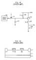
- FIG. 1Ais a circuit diagram showing a conventional CMOS image sensor whose unit pixel consists of 4 MOS transistors and 1 photodiode (PD).
- the CMOS image sensoris provided with a photodiode 100 for receiving light and for generating photo-generated charges, a transfer transistor 101 for transferring the photo-generated charges collected by the photodiode 100 to the floating diffusion region 102 , a reset transistor 103 for toning the potential of the floating diffusion region to a desired value and for resetting the floating diffusion region 102 by outputting charges, a drive transistor 104 for operating as a source follower buffer amplifier, and a select transistor for 105 for providing addressing by switching. Outside the unit pixel, there is a load transistor 106 for reading output signals.
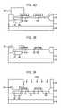
- FIG. 1B through FIG. 1Gare cross-sectional views showing the manufacturing process of forming these unit pixels, for transfer transistors and reset transistors.
- a lightly doped p-type epitaxial layer 11is formed on a heavily doped p-type substrate 10 as shown on FIG. 1B . This combination is used because the lightly doped epitaxial layer 11 improves the performance characteristics by increasing the depth of the depletion layer, and the heavily doped substrate 10 prevents crosstalk between unit pixels.
- a field oxide layer 12 defining active area and field areais formed on desired areas of the epitaxial layer using thermal oxide.
- the gates of the transfer transistor 13 a and the reset transistor 13 bare formed on the active area by depositing gate oxide (not shown), gate polysilicon 13 a and 13 b , and tungsten silicide 14 and by patterning them.
- the gates of a drive transistor Dx and a select transistor Sxare also patterned.
- a n-type ion implant region 16 for a photodiodeis formed inside the epitaxial layer 11 between the transfer transistor 13 a and the field oxide 12 by a high-energy ion implantation process.
- a low-energy ion implantation processis performed to form a p-type ion implant region 17 for photodiode between the n-type ion implant region 16 and the surface of the epitaxial layer.
- a low voltage buried photo diode(LVBPD) is completed.
- spacer insulation layer 18is deposited on the whole structure, in order to form a spacer 18 made of nitride or oxide film on the sidewalls of the gate electrode of the transistors.
- the spacer 18is formed on both sidewalls of the gate electrode as shown on FIG. 1F , by performing blanket dry etching process.
- the surface of the photodiodecan get damaged during the blanket dry etching process, causing defects in the crystal lattice structure. These defects become the source of “dark current”, or current that is caused by electrons moving from photo diode to floating diffusion region, even when there is no light present.
- This dark currentis reported to be caused by various defects (line defect, point defect, etc.) or dangling bonds, existing near the edge of the active area. The dark current can be a serious problem in low illumination environment.
- a second mask 19 for forming floating diffusion region 20 and source/drain region 21is formed, and n-type ion implantation process is performed.
- usual subsequent processesare performed to finish the unit pixel manufacturing process.
- the light incident upon the photodiodepasses through the insulation film (mostly oxides) into the epitaxial layer.
- the insulation filmmostly oxides
- CMOS image sensorreduces dark current by protecting the surface of the photodiode from the blanket dry etching using spacer etching barrier film, and therefore improves the optical properties for short wavelength light using a spacer forming insulation layer residual on the surface of the photodiode.
- a method for fabricating a CMOS image sensor comprising low voltage buried photodiode and transfer transistorcomprises: forming a field oxide for defining active area and field area on certain area of an epitaxial layer formed on a substrate, and forming a gate of transfer transistor on the epitaxial layer of the active area; forming the low voltage buried photodiode doping region in alignment with one side of the gate of transfer transistor and field oxide; forming a spacer insulation layer by stacking layers of oxide and nitride over the whole structure; forming a spacer block mask to open areas excluding doping region for the low voltage buried photodiode; and removing the spacer block mask, and forming a floating diffusion region on other side of the transfer transistor.
- FIG. 1Ais a circuit diagram of a single pixel in a conventional CMOS image sensor
- FIG. 1B through FIG. 1Gare cross-sectional views showing a method for fabricating a CMOS image sensor according to the prior art
- FIG. 2A through FIG. 2Fare cross-sectional views showing a method for fabricating a CMOS image sensor according to a first disclosed embodiment
- FIG. 3A through FIG. 3Fare cross-sectional views of showing manufacturing method of a CMOS image sensor according to a second disclosed embodiment.
- FIG. 4A through FIG. 4Care graphs showing optical properties of a short wavelength light incident upon a photodiode of a CMOS image sensor made according to the disclosed methods.
- FIGS. 2A through 2Fare cross-sectional views of disclosed manufacturing process of a CMOS image sensor with emphasis on the transfer transistor and reset transistor.
- a lightly doped p-type epitaxial layer 31is formed on the heavily doped p-type substrate 30 as shown on FIG. 2A . This combination is used because the lightly doped epitaxial layer 31 improves the performance characteristics by increasing the depth of the depletion layer, and the heavily doped substrate 30 prevents crosstalk between unit pixels.
- a component isolator 32is formed on some area of the epitaxial layer 31 .
- a field oxide using thermal oxidecan be used as component isolator, however, it is possible to use trench structure as a component isolator.
- the gates of the transfer transistor 33 a and the reset transistor 33 bare formed on the active area by depositing gate oxide (not shown), gate polysilicon 33 , and tungsten silicide 34 and by patterning them. Although not shown on FIG. 2A , gates of drive transistor Dx and select transistor Sx are patterned together.
- an ion implantation processis performed to form a low voltage buried photo diode (LVBPD).
- a screen oxide 35 for ion implantationis deposited on top of the epitaxial layer 31 where the doping region for a photodiode will be formed, to prevent damage on the surface of the semiconductor substrate.
- the screen oxide 35has a thickness ranging from about 100 to about 500 ⁇ .
- a first mask 36is formed to open the area to form the photodiode, and a n-type ion implant region 37 is formed by a high energy ion implantation process, inside the epitaxial layer 31 between the transfer transistor 33 a and the field oxide 32 .
- a low-energy ion implantation processis performed to form a p-type ion imolant region 38 for the photodiode between the n-type ion implant region 37 and the surface of the epitaxial layer.
- a low voltage buried photo diode(LVBPD) is completed.
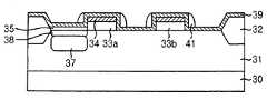
- a sacrificial nitride 39is formed on the whole structure including the gate of the transfer transistor 33 a , the gate of the reset transistor 33 b , and screen oxide 35 for ion implantation. Then a spacer insulation layer 40 is formed on the sacrificial nitride 39 .
- the sacrificial nitride 39is made to have a thickness ranging from about 100 to about 500 ⁇ .
- the sacrificial nitride 39is used to protect the surface of the photodiode during the process of forming a spacer 41 by blanket etching, and provides a good protection of the photodiode even when a considerable over-etching occurs during the blanket etching process, because the sacrificial nitride 39 has a high etching selectivity against the spacer insulation layer 40 .
- an oxide spacer 41is formed on both sidewalls of the transistor gate electrodes, by performing a blanket dry etching. Later, the residual sacrificial nitride 39 is removed by a wet etching technique. In an embodiment of the present invention, the damage to the surface of the photodiode is minimized, because a sacrificial nitride 39 is used to protect the surface of the photodiode during the blanket etching process, and a wet etching technique is used to remove the residual sacrificial nitride 39 .
- a second mask 42is formed and n-type ion implantation process is performed, to form a floating diffusion region 43 between the gate of transfer transistor 33 a and the gate of reset transistor 33 b , and a source/drain region 44 on other side of the reset transistor.
- usual subsequent processesare performed to finish the unit pixel manufacturing process.
- the residual sacrificial nitride 39is not removed and left on the surface, in order to improve the optical properties for lights of shorter wavelength, like blue light.
- the sacrificial nitride 39 in FIG. 2Eis not removed by the wet etching technique, but is allowed to remain on the surface of the photodiode to improve optical properties.
- a technique for improving optical properties for lights of shorter wavelength, like blue, using residual sacrificial nitride 39 on the surface of the photodiodeis explained.
- FIG. 3A through FIG. 3Fare cross-sections of manufacturing process of a CMOS image sensor according to the second embodiment, illustrated with emphasis on the transfer transistor and reset transistor.
- a lightly doped p-type epitaxial layer 51is formed on a heavily doped p-type substrate 50 . This combination is used because the lightly doped epitaxial layer 51 improves the performance characteristics by increasing the depth of the depletion layer, and the heavily doped substrate 50 prevents crosstalk between unit pixels.
- component isolatoris formed on desired areas of the epitaxial layer 51 .
- a field oxide 52 using thermal oxide filmis used as the component isolator.
- the field oxidewas used as the component isolator in this embodiment of the present invention, it is possible to use a component isolator using a trench structure.
- gate oxide(not shown), gate polysilicon 53 a and 53 b , and tungsten silicide 54 are sequentially deposited on the active area, and then patterned to form the gates of the transfer transistor 53 a and the reset transistor 53 b .
- the gates of a drive transistor Dx and a select transistor Sxare also patterned at this time.
- a n-type ion implant region 56 for photodiodeis formed inside the epitaxial layer 51 between the transfer transistor 53 a and the field oxide 52 by a high-energy ion implantation process.
- a low-energy ion implantation processis performed to form a p-type ion implant region 57 for the photodiode between the n-type ion implant region 56 and the surface of the epitaxial layer, by a high-energy ion implantation process.
- a low voltage buried photo diode(LVBPD) is completed.
- a spacer insulation layer 58is deposited on the entire structure, in order to form spacers on both sidewalls of the gates of the transistors.
- an insulation film of stacked layers of oxide and nitrideis used as a spacer insulation layer 58 . More specifically, an oxide layer is deposited on the epitaxial layer 51 with a thickness ranging from about 200 ⁇ to about 1000 ⁇ . On top of this layer, a nitride layer is deposited forming stacked layers, with a thickness ranging from about 200 ⁇ to about 1000 ⁇ . This is to improve the optical properties for lights of shorter wavelengh, like blue. This will be further described later.
- a spacer block mask 59is patterned, so that the spacer insulation layer 58 formed on the surface of the epitaxial layer in photodiode area is not removed during the subsequent etching process.
- the spacer block mask 59is patterned in such a way as to mask the photodiode area between the field oxide 52 and transfer transistor gate 53 a but expose other areas.
- the spacer block mask 59is easily formed by using the first mask 55 for the low voltage buried photo diode, and a negative photoresist.
- spacer block mask 59After the spacer block mask 59 is formed this way, a blanket dry etching is performed to form spacers 60 on both sidewalls of the gate, as shown on FIG. 3E . After this, the spacer block mask 59 is removed. During the blanket dry etching process, because of the existence of spacer block mask 59 , the spacer insulation layer 58 will remain intact on the photodiode.
- a second mask 61is formed to form a floating diffusion region 62 and source/drain region 63 .
- n-type ion implantation processis performed to form the floating diffusion region 62 and source/drain region 63 .
- the second mask 61is removed, and usual subsequent processes are performed to manufacture the CMOS image sensor.
- the spacer insulation layerremains on the surface of the photodiode, which prevents damage to the surface of the photodiode during the blanket dry etching process, and as a result, provides the advantage of reducing dark current.
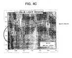
- FIG. 4A through FIG. 4Cgraphically show the results of experiments for light transmittance of lights incident upon the photodiode, when stacked layers of nitride and oxide are used as the spacer insulation layer, and the spacer insulation layer is allowed to remain on the surface of the photodiode.
- FIG. 4Ais a graph showing the light transmittance of lights incident upon the photodiode, using lights of wavelengths 0.45 ⁇ m or 0.55 ⁇ m, for two cases.
- the first caseis according to a disclosed embodiment, and an oxide layer with a thickness of about 200 ⁇ and a nitride layer with a thickness ranging from about 360 ⁇ to about 480 ⁇ are stacked on the surface of the photodiode.
- the second case(denoted ‘normal’ in FIG. 4A ) is according to the prior art.
- FIG. 4Athe average light transmittance of normal case (according to the prior art), and the average light transmittance of lights with wavelengths of 0.45 ⁇ m or 0.55 ⁇ m are shown together.
- the light transmittancehas increased for the stacked layers of nitride and oxide, compared to the case of the prior art, for lights of shorter wavelength.
- the x axisrepresents the wavelength of lights (unit: ⁇ )
- y axisrepresents light transmittance.
- FIG. 4Bis a graph showing light transmittance of lights incident upon the photodiode for two cases.
- the first caseis according to a disclosed embodiment, where an oxide layer with a thickness of about 300 ⁇ and a nitride layer with a thickness ranging from about 260 ⁇ to about 380 ⁇ are stacked on the surface of the photodiode.
- the second case(denoted ‘normal’ in FIG. 4A ) is according to the prior art.
- FIG. 4Cis a graph showing light transmittance of light incident upon the photodiode for two cases.
- the first caseis according to another embodiment, where an oxide layer with a thickness of about 500 ⁇ and a nitride layer with a thickness of about 180 ⁇ are stacked on the surface of the photodiode.
- the second case(denoted ‘normal’ in FIG. 4A ) is according to the prior art.
- light of wavelengths 0.45 ⁇ m or 0.55 ⁇ mwere used, as in FIG. 4A .
- FIG. 4B and FIG. 4Cthe average light transmittance of normal case (according to the prior art), and the average light transmittance of light with wavelengths of 0.45 ⁇ m or 0.55 ⁇ m are shown together.
- the averagesare shown as almost straight lines in both FIG. 4 b and FIG. 4C .
- the light transmittanceincreases for lights of short wavelength, including blue, when a spacer of stacked layers of nitride and oxide is used, and when the spacer is allowed to remain on the surface of the photodiode.
Landscapes
- Solid State Image Pick-Up Elements (AREA)
- Metal-Oxide And Bipolar Metal-Oxide Semiconductor Integrated Circuits (AREA)
- Transforming Light Signals Into Electric Signals (AREA)
Abstract
Description
Claims (10)
Priority Applications (1)
| Application Number | Priority Date | Filing Date | Title |
|---|---|---|---|
| US11/244,512US7183129B2 (en) | 2002-12-27 | 2005-10-05 | Method for manufacturing CMOS image sensor using spacer etching barrier film |
Applications Claiming Priority (6)
| Application Number | Priority Date | Filing Date | Title |
|---|---|---|---|
| KR10-2002-0085113AKR100494645B1 (en) | 2002-12-27 | 2002-12-27 | Method for fabricating CMOS image sensor with spacer block mask |
| KR10-2002-0085085AKR100495411B1 (en) | 2002-12-27 | 2002-12-27 | Method for fabricating CMOS image sensor with spacer etching buffer nitride layer |
| KR2002-0085085 | 2002-12-27 | ||
| KR2002-0085113 | 2002-12-27 | ||
| US10/669,996US6974715B2 (en) | 2002-12-27 | 2003-09-24 | Method for manufacturing CMOS image sensor using spacer etching barrier film |
| US11/244,512US7183129B2 (en) | 2002-12-27 | 2005-10-05 | Method for manufacturing CMOS image sensor using spacer etching barrier film |
Related Parent Applications (1)
| Application Number | Title | Priority Date | Filing Date |
|---|---|---|---|
| US10/669,996ContinuationUS6974715B2 (en) | 2002-12-27 | 2003-09-24 | Method for manufacturing CMOS image sensor using spacer etching barrier film |
Publications (2)
| Publication Number | Publication Date |
|---|---|
| US20060038248A1 US20060038248A1 (en) | 2006-02-23 |
| US7183129B2true US7183129B2 (en) | 2007-02-27 |
Family
ID=32684328
Family Applications (2)
| Application Number | Title | Priority Date | Filing Date |
|---|---|---|---|
| US10/669,996Expired - LifetimeUS6974715B2 (en) | 2002-12-27 | 2003-09-24 | Method for manufacturing CMOS image sensor using spacer etching barrier film |
| US11/244,512Expired - LifetimeUS7183129B2 (en) | 2002-12-27 | 2005-10-05 | Method for manufacturing CMOS image sensor using spacer etching barrier film |
Family Applications Before (1)
| Application Number | Title | Priority Date | Filing Date |
|---|---|---|---|
| US10/669,996Expired - LifetimeUS6974715B2 (en) | 2002-12-27 | 2003-09-24 | Method for manufacturing CMOS image sensor using spacer etching barrier film |
Country Status (3)
| Country | Link |
|---|---|
| US (2) | US6974715B2 (en) |
| JP (2) | JP2004214665A (en) |
| TW (1) | TWI332262B (en) |
Cited By (10)
| Publication number | Priority date | Publication date | Assignee | Title |
|---|---|---|---|---|
| US20060284223A1 (en)* | 2005-06-17 | 2006-12-21 | Dongbu Electronics Co., Ltd. | CMOS image sensor and manufacturing method thereof |
| US20070072325A1 (en)* | 2005-09-27 | 2007-03-29 | Omnivision Technologies, Inc. | Self-aligned photodiode for CMOS image sensor and method of making |
| US20090210968A1 (en)* | 2007-06-12 | 2009-08-20 | Nguyen Henry T | Drought Responsive Genes In Plants And Methods Of Their Use |
| US20140035105A1 (en)* | 2012-08-03 | 2014-02-06 | Kabushiki Kaisha Toshiba | Semiconductor device, method for manufacturing semiconductor device, and base member for semiconductor device formation |
| US9343489B2 (en) | 2011-05-12 | 2016-05-17 | DePuy Synthes Products, Inc. | Image sensor for endoscopic use |
| US9462234B2 (en) | 2012-07-26 | 2016-10-04 | DePuy Synthes Products, Inc. | Camera system with minimal area monolithic CMOS image sensor |
| US9825077B2 (en)* | 2006-08-02 | 2017-11-21 | Canon Kabushiki Kaisha | Photoelectric conversion device, method for producing photoelectric conversion device, and image pickup system |
| US10517469B2 (en) | 2013-03-15 | 2019-12-31 | DePuy Synthes Products, Inc. | Image sensor synchronization without input clock and data transmission clock |
| US10750933B2 (en) | 2013-03-15 | 2020-08-25 | DePuy Synthes Products, Inc. | Minimize image sensor I/O and conductor counts in endoscope applications |
| US11266305B2 (en) | 2013-02-28 | 2022-03-08 | DePuy Synthes Products, Inc. | Videostroboscopy of vocal cords with CMOS sensors |
Families Citing this family (35)
| Publication number | Priority date | Publication date | Assignee | Title |
|---|---|---|---|---|
| KR100345669B1 (en)* | 2000-08-18 | 2002-07-24 | 주식회사 하이닉스반도체 | Image sensor having nonsymmetric spacer on each side wall of transfer transistor gate electrode and method for forming the same |
| US7354789B2 (en)* | 2003-11-04 | 2008-04-08 | Dongbu Electronics Co., Ltd. | CMOS image sensor and method for fabricating the same |
| KR100603247B1 (en)* | 2003-12-31 | 2006-07-20 | 동부일렉트로닉스 주식회사 | CMOS image sensor and its manufacturing method |
| US7115438B2 (en)* | 2004-04-29 | 2006-10-03 | United Microelectronics Corp. | Method for manufacturing a complementary metal-oxide semiconductor sensor |
| KR100595875B1 (en)* | 2004-05-06 | 2006-07-03 | 매그나칩 반도체 유한회사 | Manufacturing method of CMOS image sensor with reduced etching damage |
| US20050274994A1 (en)* | 2004-06-14 | 2005-12-15 | Rhodes Howard E | High dielectric constant spacer for imagers |
| KR100660324B1 (en)* | 2004-07-01 | 2006-12-22 | 동부일렉트로닉스 주식회사 | Manufacturing Method of CMOS Image Sensor |
| KR100640531B1 (en)* | 2004-08-20 | 2006-10-30 | 동부일렉트로닉스 주식회사 | Manufacturing method of self-aligned image sensor |
| KR100741933B1 (en)* | 2004-09-21 | 2007-07-23 | 동부일렉트로닉스 주식회사 | Manufacturing Method of CMOS Image Sensor |
| KR100649022B1 (en)* | 2004-11-09 | 2006-11-28 | 동부일렉트로닉스 주식회사 | Manufacturing Method of CMOS Image Sensor |
| KR100606937B1 (en)* | 2004-11-19 | 2006-08-02 | 동부일렉트로닉스 주식회사 | Manufacturing Method of CMOS Image Sensor |
| US7592645B2 (en) | 2004-12-08 | 2009-09-22 | Canon Kabushiki Kaisha | Photoelectric conversion device and method for producing photoelectric conversion device |
| US7098067B2 (en)* | 2004-12-13 | 2006-08-29 | International Business Machines Corporation | Masked sidewall implant for image sensor |
| KR100595601B1 (en)* | 2004-12-14 | 2006-07-05 | 동부일렉트로닉스 주식회사 | CMOS image sensor manufacturing method |
| US7115925B2 (en)* | 2005-01-14 | 2006-10-03 | Omnivision Technologies, Inc. | Image sensor and pixel having an optimized floating diffusion |
| KR100672994B1 (en)* | 2005-01-28 | 2007-01-24 | 삼성전자주식회사 | Image sensor and its manufacturing method |
| KR100672688B1 (en)* | 2005-06-07 | 2007-01-22 | 동부일렉트로닉스 주식회사 | Manufacturing Method of CMOS Image Sensor |
| KR100672729B1 (en)* | 2005-07-14 | 2007-01-24 | 동부일렉트로닉스 주식회사 | Manufacturing Method of CMOS Image Sensor |
| JP2007165864A (en)* | 2005-11-15 | 2007-06-28 | Canon Inc | Photoelectric conversion device, photoelectric conversion device manufacturing method, and imaging system |
| CN1992215A (en)* | 2005-12-29 | 2007-07-04 | 东部电子股份有限公司 | Method for manufacturing cmos image sensor |
| KR100685889B1 (en)* | 2005-12-29 | 2007-02-26 | 동부일렉트로닉스 주식회사 | Manufacturing Method of CMOS Image Sensor |
| KR100760914B1 (en)* | 2005-12-29 | 2007-09-21 | 동부일렉트로닉스 주식회사 | Manufacturing Method of CMOS Image Sensor |
| KR100809322B1 (en)* | 2006-01-12 | 2008-03-05 | 삼성전자주식회사 | Image sensor manufacturing method and image sensor manufactured accordingly |
| KR100772316B1 (en)* | 2006-04-28 | 2007-10-31 | 매그나칩 반도체 유한회사 | Manufacturing Method of CMOS Image Sensor Protecting Photodiode from Plasma Damage |
| JP5157259B2 (en) | 2007-05-29 | 2013-03-06 | ソニー株式会社 | Solid-state imaging device and imaging apparatus |
| US20090121264A1 (en)* | 2007-11-12 | 2009-05-14 | Ching-Hung Kao | Cmos image sensor and method of forming the same |
| JP2009135349A (en)* | 2007-12-03 | 2009-06-18 | Panasonic Corp | MOS type solid-state imaging device and manufacturing method thereof |
| CN101533802B (en)* | 2008-03-12 | 2011-02-09 | 联华电子股份有限公司 | Complementary metal oxide semiconductor image sensor and manufacturing method thereof |
| CN101625996B (en)* | 2008-07-08 | 2011-03-23 | 中芯国际集成电路制造(上海)有限公司 | ONO side wall etching process for reducing dark current |
| DE102009039416A1 (en)* | 2009-08-31 | 2011-03-17 | Globalfoundries Dresden Module One Llc & Co. Kg | Lowered interlayer dielectric in a metallization structure of a semiconductor device |
| US9000500B2 (en)* | 2009-12-30 | 2015-04-07 | Omnivision Technologies, Inc. | Image sensor with doped transfer gate |
| JP5930650B2 (en) | 2011-10-07 | 2016-06-08 | キヤノン株式会社 | Manufacturing method of semiconductor device |
| US9147710B2 (en) | 2013-07-23 | 2015-09-29 | Taiwan Semiconductor Manufacturing Co., Ltd. | Photodiode gate dielectric protection layer |
| JP6161454B2 (en)* | 2013-07-25 | 2017-07-12 | キヤノン株式会社 | Photoelectric conversion device, manufacturing method thereof, and camera |
| JP2018101804A (en)* | 2018-03-08 | 2018-06-28 | ルネサスエレクトロニクス株式会社 | Method for manufacturing imaging device, and imaging device |
Citations (4)
| Publication number | Priority date | Publication date | Assignee | Title |
|---|---|---|---|---|
| US6166405A (en) | 1998-04-23 | 2000-12-26 | Matsushita Electronics Corporation | Solid-state imaging device |
| US6177333B1 (en)* | 1999-01-14 | 2001-01-23 | Micron Technology, Inc. | Method for making a trench isolation for semiconductor devices |
| US6180969B1 (en) | 1998-02-28 | 2001-01-30 | Hyundai Electronics Industries Co., Ltd. | CMOS image sensor with equivalent potential diode |
| US6611037B1 (en) | 2000-08-28 | 2003-08-26 | Micron Technology, Inc. | Multi-trench region for accumulation of photo-generated charge in a CMOS imager |
Family Cites Families (8)
| Publication number | Priority date | Publication date | Assignee | Title |
|---|---|---|---|---|
| JPS62131202A (en)* | 1985-12-03 | 1987-06-13 | Matsushita Electronics Corp | Process for forming color filter |
| JPH06244398A (en)* | 1993-02-19 | 1994-09-02 | Sony Corp | Photosensor of solid-state image pick-up device and manufacture thereof |
| JPH08293595A (en)* | 1995-04-20 | 1996-11-05 | Matsushita Electron Corp | Manufacture of semiconductor device |
| JP3087722B2 (en)* | 1998-05-07 | 2000-09-11 | 日本電気株式会社 | Semiconductor device and manufacturing method thereof |
| KR100291179B1 (en)* | 1998-06-29 | 2001-07-12 | 박종섭 | Cmos image sensor having a self-aligned silicide layer and method for fabricating the same |
| JP2000150857A (en)* | 1998-11-18 | 2000-05-30 | Nec Corp | Solid-state imaging device and manufacture of it |
| JP3782297B2 (en)* | 2000-03-28 | 2006-06-07 | 株式会社東芝 | Solid-state imaging device and manufacturing method thereof |
| JP2002217200A (en)* | 2001-01-22 | 2002-08-02 | Fujitsu Ltd | Method for manufacturing semiconductor device |
- 2003
- 2003-09-24USUS10/669,996patent/US6974715B2/ennot_activeExpired - Lifetime
- 2003-09-25TWTW092126469Apatent/TWI332262B/ennot_activeIP Right Cessation
- 2003-12-25JPJP2003430858Apatent/JP2004214665A/enactivePending
- 2005
- 2005-10-05USUS11/244,512patent/US7183129B2/ennot_activeExpired - Lifetime
- 2011
- 2011-10-24JPJP2011233129Apatent/JP5306436B2/ennot_activeExpired - Lifetime
Patent Citations (4)
| Publication number | Priority date | Publication date | Assignee | Title |
|---|---|---|---|---|
| US6180969B1 (en) | 1998-02-28 | 2001-01-30 | Hyundai Electronics Industries Co., Ltd. | CMOS image sensor with equivalent potential diode |
| US6166405A (en) | 1998-04-23 | 2000-12-26 | Matsushita Electronics Corporation | Solid-state imaging device |
| US6177333B1 (en)* | 1999-01-14 | 2001-01-23 | Micron Technology, Inc. | Method for making a trench isolation for semiconductor devices |
| US6611037B1 (en) | 2000-08-28 | 2003-08-26 | Micron Technology, Inc. | Multi-trench region for accumulation of photo-generated charge in a CMOS imager |
Non-Patent Citations (2)
| Title |
|---|
| Furumiya et al., "High-Sensitivity and No-Crosstalk Pixel Technology for Embedded CMOS Image Sensor", IEEE Transactions on Electron Devices, vol. 48, No. 10, Oct. 2001, pp. 2221-2227. |
| Nallapati et al., "Influence of Plasma Induced Damage During Active Etch on Silicon Defect Generation", 2000 5<SUP>th </SUP>International Symposium on Plasma Process-Induced Damage, May 23-24, Santa Clara, CA, USA, 2000 American Vacuum Society, pp. 61-64. |
Cited By (37)
| Publication number | Priority date | Publication date | Assignee | Title |
|---|---|---|---|---|
| US20060284223A1 (en)* | 2005-06-17 | 2006-12-21 | Dongbu Electronics Co., Ltd. | CMOS image sensor and manufacturing method thereof |
| US20070072325A1 (en)* | 2005-09-27 | 2007-03-29 | Omnivision Technologies, Inc. | Self-aligned photodiode for CMOS image sensor and method of making |
| US7344910B2 (en)* | 2005-09-27 | 2008-03-18 | Omnivision Technologies, Inc. | Self-aligned photodiode for CMOS image sensor and method of making |
| US9825077B2 (en)* | 2006-08-02 | 2017-11-21 | Canon Kabushiki Kaisha | Photoelectric conversion device, method for producing photoelectric conversion device, and image pickup system |
| US20090210968A1 (en)* | 2007-06-12 | 2009-08-20 | Nguyen Henry T | Drought Responsive Genes In Plants And Methods Of Their Use |
| US9907459B2 (en) | 2011-05-12 | 2018-03-06 | DePuy Synthes Products, Inc. | Image sensor with tolerance optimizing interconnects |
| US11179029B2 (en) | 2011-05-12 | 2021-11-23 | DePuy Synthes Products, Inc. | Image sensor with tolerance optimizing interconnects |
| US9622650B2 (en) | 2011-05-12 | 2017-04-18 | DePuy Synthes Products, Inc. | System and method for sub-column parallel digitizers for hybrid stacked image sensor using vertical interconnects |
| US9763566B2 (en) | 2011-05-12 | 2017-09-19 | DePuy Synthes Products, Inc. | Pixel array area optimization using stacking scheme for hybrid image sensor with minimal vertical interconnects |
| US11432715B2 (en) | 2011-05-12 | 2022-09-06 | DePuy Synthes Products, Inc. | System and method for sub-column parallel digitizers for hybrid stacked image sensor using vertical interconnects |
| US11682682B2 (en) | 2011-05-12 | 2023-06-20 | DePuy Synthes Products, Inc. | Pixel array area optimization using stacking scheme for hybrid image sensor with minimal vertical interconnects |
| US9980633B2 (en) | 2011-05-12 | 2018-05-29 | DePuy Synthes Products, Inc. | Image sensor for endoscopic use |
| US9343489B2 (en) | 2011-05-12 | 2016-05-17 | DePuy Synthes Products, Inc. | Image sensor for endoscopic use |
| US10517471B2 (en) | 2011-05-12 | 2019-12-31 | DePuy Synthes Products, Inc. | Pixel array area optimization using stacking scheme for hybrid image sensor with minimal vertical interconnects |
| US12100716B2 (en) | 2011-05-12 | 2024-09-24 | DePuy Synthes Products, Inc. | Image sensor with tolerance optimizing interconnects |
| US10537234B2 (en) | 2011-05-12 | 2020-01-21 | DePuy Synthes Products, Inc. | Image sensor with tolerance optimizing interconnects |
| US11109750B2 (en) | 2011-05-12 | 2021-09-07 | DePuy Synthes Products, Inc. | Pixel array area optimization using stacking scheme for hybrid image sensor with minimal vertical interconnects |
| US10709319B2 (en) | 2011-05-12 | 2020-07-14 | DePuy Synthes Products, Inc. | System and method for sub-column parallel digitizers for hybrid stacked image sensor using vertical interconnects |
| US11848337B2 (en) | 2011-05-12 | 2023-12-19 | DePuy Synthes Products, Inc. | Image sensor |
| US10863894B2 (en) | 2011-05-12 | 2020-12-15 | DePuy Synthes Products, Inc. | System and method for sub-column parallel digitizers for hybrid stacked image sensor using vertical interconnects |
| US11026565B2 (en) | 2011-05-12 | 2021-06-08 | DePuy Synthes Products, Inc. | Image sensor for endoscopic use |
| US9462234B2 (en) | 2012-07-26 | 2016-10-04 | DePuy Synthes Products, Inc. | Camera system with minimal area monolithic CMOS image sensor |
| US11766175B2 (en) | 2012-07-26 | 2023-09-26 | DePuy Synthes Products, Inc. | Camera system with minimal area monolithic CMOS image sensor |
| US11089192B2 (en) | 2012-07-26 | 2021-08-10 | DePuy Synthes Products, Inc. | Camera system with minimal area monolithic CMOS image sensor |
| US10701254B2 (en) | 2012-07-26 | 2020-06-30 | DePuy Synthes Products, Inc. | Camera system with minimal area monolithic CMOS image sensor |
| US10075626B2 (en) | 2012-07-26 | 2018-09-11 | DePuy Synthes Products, Inc. | Camera system with minimal area monolithic CMOS image sensor |
| US20140035105A1 (en)* | 2012-08-03 | 2014-02-06 | Kabushiki Kaisha Toshiba | Semiconductor device, method for manufacturing semiconductor device, and base member for semiconductor device formation |
| US11266305B2 (en) | 2013-02-28 | 2022-03-08 | DePuy Synthes Products, Inc. | Videostroboscopy of vocal cords with CMOS sensors |
| US11998166B2 (en) | 2013-02-28 | 2024-06-04 | DePuy Synthes Products, Inc. | Videostroboscopy of vocal cords with CMOS sensors |
| US11344189B2 (en) | 2013-03-15 | 2022-05-31 | DePuy Synthes Products, Inc. | Image sensor synchronization without input clock and data transmission clock |
| US11253139B2 (en) | 2013-03-15 | 2022-02-22 | DePuy Synthes Products, Inc. | Minimize image sensor I/O and conductor counts in endoscope applications |
| US10980406B2 (en) | 2013-03-15 | 2021-04-20 | DePuy Synthes Products, Inc. | Image sensor synchronization without input clock and data transmission clock |
| US10881272B2 (en) | 2013-03-15 | 2021-01-05 | DePuy Synthes Products, Inc. | Minimize image sensor I/O and conductor counts in endoscope applications |
| US10750933B2 (en) | 2013-03-15 | 2020-08-25 | DePuy Synthes Products, Inc. | Minimize image sensor I/O and conductor counts in endoscope applications |
| US11903564B2 (en) | 2013-03-15 | 2024-02-20 | DePuy Synthes Products, Inc. | Image sensor synchronization without input clock and data transmission clock |
| US10517469B2 (en) | 2013-03-15 | 2019-12-31 | DePuy Synthes Products, Inc. | Image sensor synchronization without input clock and data transmission clock |
| US12150620B2 (en) | 2013-03-15 | 2024-11-26 | DePuy Synthes Products, Inc. | Minimize image sensor I/O and conductor counts in endoscope applications |
Also Published As
| Publication number | Publication date |
|---|---|
| US20040129990A1 (en) | 2004-07-08 |
| JP2004214665A (en) | 2004-07-29 |
| US20060038248A1 (en) | 2006-02-23 |
| TWI332262B (en) | 2010-10-21 |
| US6974715B2 (en) | 2005-12-13 |
| JP2012044211A (en) | 2012-03-01 |
| TW200411915A (en) | 2004-07-01 |
| JP5306436B2 (en) | 2013-10-02 |
Similar Documents
| Publication | Publication Date | Title |
|---|---|---|
| US7183129B2 (en) | Method for manufacturing CMOS image sensor using spacer etching barrier film | |
| US11948956B2 (en) | Image sensors including an amorphous region and an electron suppression region | |
| US11056530B2 (en) | Semiconductor structure with metal connection layer | |
| US7338832B2 (en) | CMOS image sensor and method of fabricating the same | |
| US7217967B2 (en) | CMOS image sensor and method for manufacturing the same | |
| US7232712B2 (en) | CMOS image sensor and method for fabricating the same | |
| JP3723124B2 (en) | Solid-state imaging device | |
| US7005315B2 (en) | Method and fabricating complementary metal-oxide semiconductor image sensor with reduced etch damage | |
| TWI863756B (en) | Vertically charge transferring pixel sensor and method of manufacturing and operating the same | |
| KR100494645B1 (en) | Method for fabricating CMOS image sensor with spacer block mask | |
| US7868364B2 (en) | Image sensor | |
| JP2005129965A (en) | Solid-state imaging device | |
| KR100495411B1 (en) | Method for fabricating CMOS image sensor with spacer etching buffer nitride layer | |
| KR100815937B1 (en) | Image sensor and its manufacturing method | |
| KR100535920B1 (en) | Method for fabricating CMOS Image sensor | |
| KR100461971B1 (en) | CMOS image sensor with protecting heavy metal ions for reducing dark current | |
| KR20030056060A (en) | Image sensor with improved charge capacity and fabricating method of the same |
Legal Events
| Date | Code | Title | Description |
|---|---|---|---|
| STCF | Information on status: patent grant | Free format text:PATENTED CASE | |
| FEPP | Fee payment procedure | Free format text:PAYOR NUMBER ASSIGNED (ORIGINAL EVENT CODE: ASPN); ENTITY STATUS OF PATENT OWNER: LARGE ENTITY | |
| AS | Assignment | Owner name:MAGNACHIP SEMICONDUCTOR, LTD., KOREA, REPUBLIC OF Free format text:ASSIGNMENT OF ASSIGNORS INTEREST;ASSIGNOR:HYNIX SEMICONDUCTOR INC.;REEL/FRAME:022288/0934 Effective date:20090219 | |
| AS | Assignment | Owner name:CROSSTEK CAPITAL, LLC, DELAWARE Free format text:ASSIGNMENT OF ASSIGNORS INTEREST;ASSIGNOR:MAGNACHIP SEMICONDUCTOR, LTD.;REEL/FRAME:022764/0270 Effective date:20090514 Owner name:CROSSTEK CAPITAL, LLC,DELAWARE Free format text:ASSIGNMENT OF ASSIGNORS INTEREST;ASSIGNOR:MAGNACHIP SEMICONDUCTOR, LTD.;REEL/FRAME:022764/0270 Effective date:20090514 | |
| FEPP | Fee payment procedure | Free format text:PAYOR NUMBER ASSIGNED (ORIGINAL EVENT CODE: ASPN); ENTITY STATUS OF PATENT OWNER: LARGE ENTITY Free format text:PAYER NUMBER DE-ASSIGNED (ORIGINAL EVENT CODE: RMPN); ENTITY STATUS OF PATENT OWNER: LARGE ENTITY | |
| FPAY | Fee payment | Year of fee payment:4 | |
| AS | Assignment | Owner name:INTELLECTUAL VENTURES II LLC, DELAWARE Free format text:MERGER;ASSIGNOR:CROSSTEK CAPITAL, LLC;REEL/FRAME:026637/0632 Effective date:20110718 | |
| AS | Assignment | Owner name:HYNIX SEMICONDUCTOR INC., KOREA, DEMOCRATIC PEOPLE Free format text:ASSIGNMENT OF ASSIGNORS INTEREST;ASSIGNOR:LEE, JU-IL;REEL/FRAME:032683/0602 Effective date:20040116 | |
| AS | Assignment | Owner name:INTELLECTUAL VENTURES FUND 99 LLC, NEVADA Free format text:ASSIGNMENT OF ASSIGNORS INTEREST;ASSIGNOR:INTELLECTUAL VENTURES II LLC;REEL/FRAME:033039/0775 Effective date:20140603 | |
| FPAY | Fee payment | Year of fee payment:8 | |
| AS | Assignment | Owner name:TARSIUM B.V., NETHERLANDS Free format text:ASSIGNMENT OF ASSIGNORS INTEREST;ASSIGNOR:INTELLECTUAL VENTURES FUND 99 LLC;REEL/FRAME:042172/0466 Effective date:20141117 Owner name:CARL ZEISS SMT GMBH, GERMANY Free format text:NUNC PRO TUNC ASSIGNMENT;ASSIGNOR:TARSIUM B.V.;REEL/FRAME:042172/0767 Effective date:20161213 Owner name:ASML NETHERLANDS B.V., NETHERLANDS Free format text:NUNC PRO TUNC ASSIGNMENT;ASSIGNOR:TARSIUM B.V.;REEL/FRAME:042172/0767 Effective date:20161213 | |
| AS | Assignment | Owner name:CARL ZEISS AG, GERMANY Free format text:NUNC PRO TUNC ASSIGNMENT;ASSIGNOR:CARL ZEISS SMT GMBH;REEL/FRAME:042307/0072 Effective date:20161223 | |
| MAFP | Maintenance fee payment | Free format text:PAYMENT OF MAINTENANCE FEE, 12TH YEAR, LARGE ENTITY (ORIGINAL EVENT CODE: M1553); ENTITY STATUS OF PATENT OWNER: LARGE ENTITY Year of fee payment:12 |