US7180135B1 - Double gate (DG) SOI ratioed logic with intrinsically on symmetric DG-MOSFET load - Google Patents
Double gate (DG) SOI ratioed logic with intrinsically on symmetric DG-MOSFET loadDownload PDFInfo
- Publication number
- US7180135B1 US7180135B1US10/951,695US95169504AUS7180135B1US 7180135 B1US7180135 B1US 7180135B1US 95169504 AUS95169504 AUS 95169504AUS 7180135 B1US7180135 B1US 7180135B1
- Authority
- US
- United States
- Prior art keywords
- adg
- sdg
- area connected
- gate
- terminal
- Prior art date
- Legal status (The legal status is an assumption and is not a legal conclusion. Google has not performed a legal analysis and makes no representation as to the accuracy of the status listed.)
- Expired - Fee Related, expires
Links
Images


Classifications
- H—ELECTRICITY
- H10—SEMICONDUCTOR DEVICES; ELECTRIC SOLID-STATE DEVICES NOT OTHERWISE PROVIDED FOR
- H10D—INORGANIC ELECTRIC SEMICONDUCTOR DEVICES
- H10D30/00—Field-effect transistors [FET]
- H10D30/60—Insulated-gate field-effect transistors [IGFET]
- H10D30/67—Thin-film transistors [TFT]
- H10D30/6729—Thin-film transistors [TFT] characterised by the electrodes
- H10D30/673—Thin-film transistors [TFT] characterised by the electrodes characterised by the shapes, relative sizes or dispositions of the gate electrodes
- H10D30/6733—Multi-gate TFTs
- H10D30/6734—Multi-gate TFTs having gate electrodes arranged on both top and bottom sides of the channel, e.g. dual-gate TFTs
- H—ELECTRICITY
- H10—SEMICONDUCTOR DEVICES; ELECTRIC SOLID-STATE DEVICES NOT OTHERWISE PROVIDED FOR
- H10D—INORGANIC ELECTRIC SEMICONDUCTOR DEVICES
- H10D86/00—Integrated devices formed in or on insulating or conducting substrates, e.g. formed in silicon-on-insulator [SOI] substrates or on stainless steel or glass substrates
- H10D86/201—Integrated devices formed in or on insulating or conducting substrates, e.g. formed in silicon-on-insulator [SOI] substrates or on stainless steel or glass substrates the substrates comprising an insulating layer on a semiconductor body, e.g. SOI
Definitions
- the present inventionrelates to the field of Silicon-On-Insulator (SOI) Metal-Oxide Semiconductor Field-Effect Transistor (MOSFET) circuitry.
- SOISilicon-On-Insulator
- MOSFETMetal-Oxide Semiconductor Field-Effect Transistor
- the present inventioninvolves ratioed logic with intrinsically ON symmetric double-gate (DG) SOI MOSFET loads.
- DGsymmetric double-gate
- DG SOI MOSFET designsas enabling Silicon (Si) devices for the 0.05 ⁇ m node and beyond.
- SiSilicon
- a number of DG structureshave been proposed and analyzed. Many of these structures have been categorized as symmetric (SDG), where both gates are made of the same polysilicon type (usually n + ), and asymmetric (ADG), where one gate is n+ and the other gate is p+ type polysilicon.
- SDGsymmetric
- ADGasymmetric
- the n+ gate SDGis usually a “normally on” device having a negative threshold voltage. Therefore, one may need to use exotic gate materials (such as metal gates with appropriate work function values), which may require expensive and complicated processing steps.
- DGDouble Gate
- basic elements of the structureincluding: a source, drain, front gate, and back gate.
- the channel lengthis shown as LG.
- Different node voltages showninclude: front gate voltage 201 ; drain voltage 202 ; source voltage 203 , and back gate voltage 204 .
- Also illustratedare several thicknesses, including silicon thickness (t Si ) 205 , front gate oxide thickness (t oxf ) 206 , and back gate oxide thickness (t oxb ) 207 .
- Designs using SDG gatesoften require fine-tuning an SDG gate using expensive and complicated processing techniques. For this and other reasons, designs implementing ADG devices have been favored.
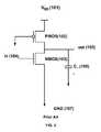
- FIG. 2shows a basic Pseudo-nMOS logic design, in which both PMOS and NMOS transistors are combined to produce logic elements.
- PMOS gate 102is tied to ground 107 and has its source tied to V DD 101 .
- NMOS gate 103is tied to input 104 , and its source is tied to GND 107 .
- the junction of PMOS 102 drain and NMOS 103 sourceforms the output 105 .
- C L 106is the load capacitance.
- Pseudo-nMOSFET or ratioed logic designshave been known to be fast and small and offer small parasitic capacitance (hence a smaller load). The main drawback of these pseudo-nMOS designs have been their consumption of high static power.
- DG MOSFETsmay be a better technology choice for the cutting edge nano-scale circuits.
- DG MOSFETsmay also be capable of offering higher drive current and transconductance.
- SDGsymmetric
- ADGasymmetric
- CMOS-based logicsare not good when considering dynamic power dissipation problems, which are prominent factors compared to static power at high frequency operation. CMOS-based logic also suffer from the larger number (2n) of devices problem.
- this new gate constructionwill be a flexible building block capable of being used to construct a set of basic logic operations with a minimal number of devices.
- One advantage of this inventionis that only one type of diffusion (nMOSFET) may be needed for constructing basic devices such as inverters, wherein traditional CMOS devices require both (n and p) type diffusion.
- Another advantage of the present inventionis that it may require only a simple dual poly (n+/p+) process in fabricating gates.
- a further advantage of this inventionis that it may provide for faster response characteristics at higher frequencies than equivalent CMOS devices.
- a further advantage of this inventionis that it may provide for devices that dissipate less power than equivalent CMOS devices.
- a further advantage of this inventionis that it may require fewer devices to build more complex multi-input gates without performance penalties.
- a further advantage of this inventionis that it may take advantage of the “normally on” state of an SDG gate.
- an SOI MOSFET invertercomprising a multitude of terminals including an SDG load structure and an ADG load structure.
- the multitude of terminalsmay include an input terminal; an output terminal; a supply voltage terminal; and a ground terminal.
- the SDG load structuremay include a first SDG junction having an n+ area connected to the supply voltage terminal; a second SDG junction having an n+ area connected to the output terminal; a first SDG gate having an n+ polysilicon area connected to the output terminal; and a second SDG gate having an n+ polysilicon area connected to the output terminal.
- the ADG load structuremay include a first ADG junction having an n+ area connected to the ground terminal; a second ADG junction having an n+ area connected to the output terminal; a first ADG gate having an n+ polysilicon area connected to the input terminal; and a second ADG gate having an p+ polysilicon area connected to the input terminal.
- the SDG load structure and the ADG load structureare constructed to satisfy an SDG load inverter ratio.
- a load capacitormay be connected between the ground terminal and the output terminal.
- Both the ADG driver structure and the SDG load structuremay be fabricated on the same substrate, may have buried gates, and may be fabricated using a dual poly process.
- a two input SOI MOSFET NOR circuitwhich includes a multitude of terminals, an SDG load structure, and an ADG load structure.
- the terminalsmay include a first input terminal; a second input terminal; an output terminal; a supply voltage terminal; and a ground terminal.
- the SDG load structuremay include a first SDG junction having an n+ area connected to the supply voltage terminal; a second SDG junction having an n+ area connected to the output terminal; a first SDG gate having an n+ polysilicon area connected to the output terminal; and a second SDG gate having an n+ polysilicon area connected to the output terminal.
- the ADG load structuremay include a first ADG junction having an n+ area connected to the ground terminal; a second ADG junction having an n+ area connected to the output terminal; a first ADG gate having an n+ polysilicon area connected to input1 terminal; and a second ADG gate having a p+ polysilicon area connected to input2 terminal.
- the SDG load structure and the ADG load structureare constructed to satisfy an SDG load inverter ratio.
- a load capacitormay be connected between the ground terminal and the output terminal.
- Both the ADG driver structure and the SDG load structuremay be fabricated on the same substrate, may have buried gates, and may be fabricated using a dual poly process.
- an n input NOR circuitwhich includes a multitude of terminals, an SDG load structure, and n/2 ADG driver structures.
- the terminalsmay include n input terminals; an output terminal; a supply voltage terminal; and a ground terminal.
- the SDG load structuremay include a first SDG junction having an n+ area connected to the supply voltage terminal; a second SDG junction having an n+ area connected to the output terminal; an first SDG gate having an n+ polysilicon area connected to the output terminal; and a second SDG gate having an n+ polysilicon area connected to the output terminal.
- Each of the n/2 ADG driver structuresmay include a first ADG junction having an n+ area connected to the ground terminal; a second ADG junction having an n+ area connected to the output terminal; a first ADG gate having an n+ polysilicon area connected to one of the input terminals; and a second ADG gate having a p+ polysilicon area connected to another of the input terminals.
- at least one of the n/2 ADG driver structures and the SDG load structureare constructed to satisfy an SDG load inverter ratio.
- a load capacitormay be connected between the ground terminal and the output terminal.
- Both the n/2 ADG driver structures and the SDG load structuremay be fabricated on the same substrate, may have buried gates, and may be fabricated using a dual poly process.
- FIG. 1shows a block diagram of a basic Double Gate (DG) structure. (prior art).
- FIG. 2shows a block diagram of a basic pseudo-nMOS/ratioed logic. (prior art).
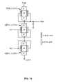
- FIG. 3shows a block diagram of a basic inverter circuit comprising a Symmetric Double Gate (SDG) SOI load nMOSEFT and an Asymmetric Double Gate (ADG) SOI driver nMOSFET as per an aspect of an embodiment of the present invention.
- SDGSymmetric Double Gate
- ADGAsymmetric Double Gate
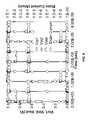
- FIG. 4shows voltage transfer characteristics for the basic inverter structure shown in FIG. 1 in comparison with an equivalent regular CMOS based DG inverter.
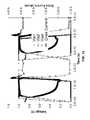
- FIG. 5shows the transient voltage and drive current characteristics for the basic inverter structure shown in FIG. 3 .
- FIG. 6shows a block diagram of a two input NOR gate as per an aspect of an embodiment of the present invention.
- FIG. 7shows the transient voltage and drive current characteristics for the two input NOR gate shown in FIG. 6 .
- FIG. 8shows a block diagram of a NAND2 gate as per an aspect of an embodiment of the present invention.
- FIG. 9shows the transient voltage and drive current characteristics for the NAND2 gate shown in FIG. 8 .
- FIG. 10shows a block diagram of a NAND2 gate as per an aspect of an embodiment of the present invention.
- FIG. 11shows the transient voltage and drive current characteristics for the NAND2 gate shown in FIG. 10 .
- FIG. 12shows a block diagram of a XOR2 gate as per an aspect of an embodiment of the present invention.
- FIG. 13shows the transient voltage and drive current characteristics for the XOR2 gate shown in FIG. 12 .
- the present inventionis an SOI Logic family composed of an intrinsically on symmetric fully depleted double gate MOSFET load and an asymmetric fully depleted double gate MOSFETs as the drivers.
- This inventionmay provide a high speed low power logic family for double gate SOI technology.
- the basic element of the digital circuitis the digital inverter, which provides a digital output signal that is the digital complement of the input. For example, if the input is “HIGH,” then the output is “LOW,” and vice versa.
- the parametersincludes a noise margin, which should be high, a threshold voltage, and load current characteristics vs. output voltage.
- Load transistor 301is a double gate NMOS transistor with the front 304 and the back 305 gates preferably formed of the same n+ poly material. The gates are connected together and connected to output node 307 .
- the driver transistor 308is a double gate NMOS transistor with a front gate 312 constructed of p+ material and a back gate 314 constructed of n+ material. These gates are connected together and connected to input node 313 of the inverter.
- the transistormay be formed of a single continuous diffusion.
- the doping of the transistor bodies 303 and 311may be undoped or lightly p doped with a doping up to 10 16 cm ⁇ 3 . Having a lightly doped body preferably helps increase mobility, reduce short channel effects, and increase the reliability of the device.
- the sources 302 and 315 and the drains 306 and 310 of the transistorsare highly n doped with doping levels in the range of 10 20 –10 21 cm ⁇ 3 .
- the Si film thicknessshould be up to 15 nm.
- the front gates 304 and 312 , as well as the back gates 305 and 314should have an ultra-thin oxide thickness (t oxf and t oxb ) up to 3 nm.
- the lengths of the front and back gates of the two transistorsmay be up to 50 nm.
- the symmetric DG NMOS transistor 301should be smaller than the asymmetric DG NMOS transistor 308 so that the D.C. power dissipation will not be high and the noise margin for the low output will be not be low.
- a preferred ratio sizehas the width of the symmetric transistor approximately half the width of the asymmetric transistor.
- Line 401represents the SDG CMOS load inverter and line 402 represents the ADG inverter.
- ratio values of 1:2have been identified for the presently described best mode, it is anticipated that other ratio values that produce useful characteristics worthy of practice may be identified for this and other embodiments.
- FIG. 5shows the transient voltage and drive current characteristics for the basic inverter structure shown in FIG. 1 with a load capacitor connected.
- the inverter operationis pulse stimulated.
- the output voltage 501is the inverted version of the input voltage 502 .
- the maximum value of the supply current 503is not that high indicating that the static current is not the main reason for power dissipation as the dynamic power increases at high frequencies approaching 2 GHz.
- FIG. 6shows a block diagram of a two input NOR gate as per an aspect of an embodiment of the present invention.
- This two input NOR gateuses the basic inverter structure described in FIG. 1 .
- one gate of the ADG nMOSFET drivershould form one input while the other gate should drive the other input.
- the expansion of the inverter circuit to a NOR2 circuitmay be achieved by decoupling the front gate 613 and back gate 615 of the asymmetric transistor 608 , and connecting inputs 611 and 612 each to one of the gates of the asymmetric transistor 608 .
- the design of the transistors to operate as a NOR gatefollows the same basic design as the inverter mentioned above. The main difference is in the width ratio.
- the width of the symmetric transistor in the NOR circuitis preferably “ON” one quarter of the time of the asymmetric transistor for better performance.
- the described logic gatesmay be better when used at high frequencies (>1 GHz), where their performance may exceed normal CMOS circuits.
- the NOR circuitsmay be extended to more than two inputs by adding more transistors in parallel.
- FIG. 7shows transient voltage and drive current characteristics for the basic inverter structure shown in FIG. 6 .
- the output 703is the result of the logic NOR operation of the input 701 and input 702 .
- NAND and XOR gateswill now be disclosed that extend this logic family of ratioed logic where an SDG device is used as the load, and an ADG devices are used as drivers.
- FIG. 8shows the first type of NAND circuit: the “driver” device is an ADG PMOS 801 connected to VDD 818 and the load is an (intrinsically on) SDG device 808 connected to GND 814 .
- the transient output voltage and driver current characteristics of this NAND2 gate for both inputs driven by 3.64 GHz pulsesis shown in FIG. 11 .
- the fabrication of this structuremay require only one (continuous) diffusion, but may need one more device to achieve the NAND operation. As is common in ratioed logic, it exhibits a non-zero LOW output signal, whereas the previous NAND2 ( FIG. 8 ) exhibits a (complementary) non VDD HIGH, because here the active load is the pull-down device. This may actually offer more flexibility to a circuit designer to choose between these two structures according to needs and constraints.
- the present inventionmay be used to construct an XOR gate using only two driver transistors, which is impossible in normal (classical) CMOS logic.
- An embodiment of an XOR gate according to the present inventionis shown in FIG. 12 and has the same base structure as the NAND2 gate shown in FIG. 10 .
- the XOR operationis possible when each asymmetric transistor 1220 and 1230 has one input 1221 and 1231 and the complement of the other input 1222 and 1232 as the two gate voltages. Therefore, the subtlety lies in the selection of the gate bias and gate-material.
- the working set of inputs and gate material combinationmay be unique and is shown in FIG. 12 . Let us consider the (10) and (01) case. These two conditions should be identical and the current would pass through the lower transistor.
- This complementary and opposite input configurationpreferably averages out both the (10) and (01) condition and produces an identical high output. Also, for (00) and (11), one may need to get the same low output. In this case, the gate configuration may stop the current from passing through the lower transistor so that an identical low voltage can be achieved at the output. Besides the appropriate gate materials and input bias combination conditions, proper sizing of the transistors may be mandatory to achieve optimum operation. Another interesting feature of this design is that the same style can be used for both XOR and NAND operation with a proper bias and gate material combination.
- a typical transient for output voltage and drive current for an XOR operationis shown in FIG. 13 with two inputs of 3.64 GHz and 2.0 GHz, respectively.
- these structurescan be further extended to other logic gates such as AOI and OAI, and to larger gates such as NOR4 or NAND4, where one only needs to add an additional parallel device for an additional 2 inputs (if a proper device sizing is used).
- CMOScomplementary metal-oxide-semiconductor
- NAND and XORtwo basic gates (NAND and XOR) which use the unique ratioed logic based approach with SDG SOI loads and ADG drivers. Together, these logic elements form a complete set of working gates, with interesting advantages and some design flexibility. It is envisioned that all of the disclosed gate topologies presented may be further improved with clocked loads to reduce power dissipation and improve signal integrity.
Landscapes
- Metal-Oxide And Bipolar Metal-Oxide Semiconductor Integrated Circuits (AREA)
- Logic Circuits (AREA)
Abstract
Description
Claims (21)
Priority Applications (1)
| Application Number | Priority Date | Filing Date | Title |
|---|---|---|---|
| US10/951,695US7180135B1 (en) | 2003-10-06 | 2004-09-29 | Double gate (DG) SOI ratioed logic with intrinsically on symmetric DG-MOSFET load |
Applications Claiming Priority (2)
| Application Number | Priority Date | Filing Date | Title |
|---|---|---|---|
| US50827603P | 2003-10-06 | 2003-10-06 | |
| US10/951,695US7180135B1 (en) | 2003-10-06 | 2004-09-29 | Double gate (DG) SOI ratioed logic with intrinsically on symmetric DG-MOSFET load |
Publications (1)
| Publication Number | Publication Date |
|---|---|
| US7180135B1true US7180135B1 (en) | 2007-02-20 |
Family
ID=37744966
Family Applications (1)
| Application Number | Title | Priority Date | Filing Date |
|---|---|---|---|
| US10/951,695Expired - Fee RelatedUS7180135B1 (en) | 2003-10-06 | 2004-09-29 | Double gate (DG) SOI ratioed logic with intrinsically on symmetric DG-MOSFET load |
Country Status (1)
| Country | Link |
|---|---|
| US (1) | US7180135B1 (en) |
Cited By (24)
| Publication number | Priority date | Publication date | Assignee | Title |
|---|---|---|---|---|
| US20070278572A1 (en)* | 2006-05-31 | 2007-12-06 | Ibrahim Ban | Asymmetric channel doping for improved memory operation for floating body cell (FBC) memory |
| US20080142907A1 (en)* | 2006-12-18 | 2008-06-19 | Franz Kuttner | Isolated multigate fet circuit blocks with different ground potentials |
| US20080285349A1 (en)* | 2007-05-15 | 2008-11-20 | Walker Andrew J | Nonvolatile memory with backplate |
| US20080303593A1 (en)* | 2007-06-11 | 2008-12-11 | Infineon Technologies Agam Campeon | Mugfet circuit for increasing output resistance |
| WO2010007478A1 (en)* | 2008-06-13 | 2010-01-21 | Yale University | Improved complementary metal oxide semiconductor devices |
| US20100079169A1 (en)* | 2008-10-01 | 2010-04-01 | Samsung Electronics Co., Ltd. | Inverter, method of operating the same and logic circuit comprising inverter |
| US20100096700A1 (en)* | 2006-12-28 | 2010-04-22 | Commissariat A L'energie Atomique | Method for fabricating asymmetric double-gate transistors by which asymmetric and symmetric double-gate transistors can be made on the same substrate |
| US20110215407A1 (en)* | 2010-03-02 | 2011-09-08 | Micron Technology, Inc. | Semiconductor-metal-on-insulator structures, methods of forming such structures, and semiconductor devices including such structures |
| US20110291171A1 (en)* | 2010-05-25 | 2011-12-01 | International Business Machines Corporation | Varactor |
| WO2012118614A3 (en)* | 2011-03-01 | 2012-11-22 | Micron Technology, Inc. | Gated bipolar junction transistors, memory arrays, and methods of forming gated bipolar junction transistors |
| WO2013026237A1 (en)* | 2011-08-22 | 2013-02-28 | 中国科学院微电子研究所 | Semiconductor device |
| US8809145B2 (en) | 2010-03-02 | 2014-08-19 | Micron Technology, Inc. | Semiconductor cells, arrays, devices and systems having a buried conductive line and methods for forming the same |
| US20140266304A1 (en)* | 2011-09-28 | 2014-09-18 | Semiconductor Energy Laboratory Co., Ltd. | Shift register circuit |
| US8841715B2 (en) | 2010-03-02 | 2014-09-23 | Micron Technology, Inc. | Floating body cell structures, devices including same, and methods for forming same |
| US8980699B2 (en) | 2010-03-02 | 2015-03-17 | Micron Technology, Inc. | Thyristor-based memory cells, devices and systems including the same and methods for forming the same |
| US9012963B2 (en) | 2011-08-22 | 2015-04-21 | Institute of Microelectronics, Chinese Academy of Sciences | Semiconductor device |
| US9129983B2 (en) | 2011-02-11 | 2015-09-08 | Micron Technology, Inc. | Memory cells, memory arrays, methods of forming memory cells, and methods of forming a shared doped semiconductor region of a vertically oriented thyristor and a vertically oriented access transistor |
| US9269795B2 (en) | 2011-07-26 | 2016-02-23 | Micron Technology, Inc. | Circuit structures, memory circuitry, and methods |
| US9361966B2 (en) | 2011-03-08 | 2016-06-07 | Micron Technology, Inc. | Thyristors |
| US20170103979A1 (en)* | 2015-10-13 | 2017-04-13 | University Of Notre Dame Du Lac | Systems and methods for filtering and computation using tunnelling transistors |
| US9646869B2 (en) | 2010-03-02 | 2017-05-09 | Micron Technology, Inc. | Semiconductor devices including a diode structure over a conductive strap and methods of forming such semiconductor devices |
| US20170324385A1 (en)* | 2016-05-06 | 2017-11-09 | Globalfoundries Inc. | Method, apparatus and system for back gate biasing for fd-soi devices |
| CN110277387A (en)* | 2018-03-13 | 2019-09-24 | 意法半导体有限公司 | inverter circuit |
| CN111710665A (en)* | 2020-07-13 | 2020-09-25 | 山东晶导微电子股份有限公司 | A voltage doubling rectifier module and a voltage doubling rectifier circuit using the same |
Citations (1)
| Publication number | Priority date | Publication date | Assignee | Title |
|---|---|---|---|---|
| US20060012405A1 (en)* | 2004-07-19 | 2006-01-19 | Martins Marcus M | Dual polarity, high input voltage swing comparator using MOS input transistors |
- 2004
- 2004-09-29USUS10/951,695patent/US7180135B1/ennot_activeExpired - Fee Related
Patent Citations (1)
| Publication number | Priority date | Publication date | Assignee | Title |
|---|---|---|---|---|
| US20060012405A1 (en)* | 2004-07-19 | 2006-01-19 | Martins Marcus M | Dual polarity, high input voltage swing comparator using MOS input transistors |
Cited By (54)
| Publication number | Priority date | Publication date | Assignee | Title |
|---|---|---|---|---|
| US20100072533A1 (en)* | 2006-05-31 | 2010-03-25 | Ibrahim Ban | Asymmetric channel doping for improved memory operation for floating body cell (fbc) memory |
| US7646071B2 (en)* | 2006-05-31 | 2010-01-12 | Intel Corporation | Asymmetric channel doping for improved memory operation for floating body cell (FBC) memory |
| US20070278572A1 (en)* | 2006-05-31 | 2007-12-06 | Ibrahim Ban | Asymmetric channel doping for improved memory operation for floating body cell (FBC) memory |
| US7944003B2 (en) | 2006-05-31 | 2011-05-17 | Intel Corporation | Asymmetric channel doping for improved memory operation for floating body cell (FBC) memory |
| US20080142907A1 (en)* | 2006-12-18 | 2008-06-19 | Franz Kuttner | Isolated multigate fet circuit blocks with different ground potentials |
| US8368144B2 (en)* | 2006-12-18 | 2013-02-05 | Infineon Technologies Ag | Isolated multigate FET circuit blocks with different ground potentials |
| US8399316B2 (en)* | 2006-12-28 | 2013-03-19 | Commissariat A L'energie Atomique | Method for making asymmetric double-gate transistors |
| US8324057B2 (en)* | 2006-12-28 | 2012-12-04 | Commissariat A L'energie Atomique | Method for fabricating asymmetric double-gate transistors by which asymmetric and symmetric double-gate transistors can be made on the same substrate |
| US20100096700A1 (en)* | 2006-12-28 | 2010-04-22 | Commissariat A L'energie Atomique | Method for fabricating asymmetric double-gate transistors by which asymmetric and symmetric double-gate transistors can be made on the same substrate |
| US20100178743A1 (en)* | 2006-12-28 | 2010-07-15 | Commissariat A L'energie Atomique | Method for making asymmetric double-gate transistors |
| US20080285349A1 (en)* | 2007-05-15 | 2008-11-20 | Walker Andrew J | Nonvolatile memory with backplate |
| US20080286925A1 (en)* | 2007-05-15 | 2008-11-20 | Walker Andrew J | Nonvolatile memory with backplate |
| US7638836B2 (en)* | 2007-05-15 | 2009-12-29 | Schiltron Corporation | Nonvolatile memory with backplate |
| US20080303593A1 (en)* | 2007-06-11 | 2008-12-11 | Infineon Technologies Agam Campeon | Mugfet circuit for increasing output resistance |
| US7667499B2 (en)* | 2007-06-11 | 2010-02-23 | Infineon Technologies Ag | MuGFET circuit for increasing output resistance |
| US8384156B2 (en) | 2008-06-13 | 2013-02-26 | Yale University | Complementary metal oxide semiconductor devices |
| US20110187412A1 (en)* | 2008-06-13 | 2011-08-04 | Tso-Ping Ma | Complementary metal oxide semiconductor devices |
| WO2010007478A1 (en)* | 2008-06-13 | 2010-01-21 | Yale University | Improved complementary metal oxide semiconductor devices |
| US20100079169A1 (en)* | 2008-10-01 | 2010-04-01 | Samsung Electronics Co., Ltd. | Inverter, method of operating the same and logic circuit comprising inverter |
| EP2172972A3 (en)* | 2008-10-01 | 2011-12-21 | Samsung Electronics Co., Ltd. | Inverter, method of operating the same and logic circuit comprising inverter |
| US8217680B2 (en) | 2008-10-01 | 2012-07-10 | Samsung Electronics Co., Ltd. | Method of operating inverter |
| US20110175647A1 (en)* | 2008-10-01 | 2011-07-21 | Sangwook Kim | Method of operating inverter |
| US7940085B2 (en)* | 2008-10-01 | 2011-05-10 | Samsung Electronics Co., Ltd. | Inverter, method of operating the same and logic circuit comprising inverter |
| US8809145B2 (en) | 2010-03-02 | 2014-08-19 | Micron Technology, Inc. | Semiconductor cells, arrays, devices and systems having a buried conductive line and methods for forming the same |
| US9608119B2 (en) | 2010-03-02 | 2017-03-28 | Micron Technology, Inc. | Semiconductor-metal-on-insulator structures, methods of forming such structures, and semiconductor devices including such structures |
| US10325926B2 (en) | 2010-03-02 | 2019-06-18 | Micron Technology, Inc. | Semiconductor-metal-on-insulator structures, methods of forming such structures, and semiconductor devices including such structures |
| US9646869B2 (en) | 2010-03-02 | 2017-05-09 | Micron Technology, Inc. | Semiconductor devices including a diode structure over a conductive strap and methods of forming such semiconductor devices |
| US20110215407A1 (en)* | 2010-03-02 | 2011-09-08 | Micron Technology, Inc. | Semiconductor-metal-on-insulator structures, methods of forming such structures, and semiconductor devices including such structures |
| US10157769B2 (en) | 2010-03-02 | 2018-12-18 | Micron Technology, Inc. | Semiconductor devices including a diode structure over a conductive strap and methods of forming such semiconductor devices |
| US8841715B2 (en) | 2010-03-02 | 2014-09-23 | Micron Technology, Inc. | Floating body cell structures, devices including same, and methods for forming same |
| US8859359B2 (en) | 2010-03-02 | 2014-10-14 | Micron Technology, Inc. | Floating body cell structures, devices including same, and methods for forming same |
| US8866209B2 (en) | 2010-03-02 | 2014-10-21 | Micron Technology, Inc. | Semiconductor cells, arrays, devices and systems having a buried conductive line and methods for forming the same |
| US8980699B2 (en) | 2010-03-02 | 2015-03-17 | Micron Technology, Inc. | Thyristor-based memory cells, devices and systems including the same and methods for forming the same |
| US20110291171A1 (en)* | 2010-05-25 | 2011-12-01 | International Business Machines Corporation | Varactor |
| US9129983B2 (en) | 2011-02-11 | 2015-09-08 | Micron Technology, Inc. | Memory cells, memory arrays, methods of forming memory cells, and methods of forming a shared doped semiconductor region of a vertically oriented thyristor and a vertically oriented access transistor |
| US8952418B2 (en) | 2011-03-01 | 2015-02-10 | Micron Technology, Inc. | Gated bipolar junction transistors |
| WO2012118614A3 (en)* | 2011-03-01 | 2012-11-22 | Micron Technology, Inc. | Gated bipolar junction transistors, memory arrays, and methods of forming gated bipolar junction transistors |
| US10886273B2 (en) | 2011-03-01 | 2021-01-05 | Micron Technology, Inc. | Gated bipolar junction transistors, memory arrays, and methods of forming gated bipolar junction transistors |
| US10373956B2 (en) | 2011-03-01 | 2019-08-06 | Micron Technology, Inc. | Gated bipolar junction transistors, memory arrays, and methods of forming gated bipolar junction transistors |
| US9361966B2 (en) | 2011-03-08 | 2016-06-07 | Micron Technology, Inc. | Thyristors |
| US9691465B2 (en) | 2011-03-08 | 2017-06-27 | Micron Technology, Inc. | Thyristors, methods of programming thyristors, and methods of forming thyristors |
| US9269795B2 (en) | 2011-07-26 | 2016-02-23 | Micron Technology, Inc. | Circuit structures, memory circuitry, and methods |
| US9012963B2 (en) | 2011-08-22 | 2015-04-21 | Institute of Microelectronics, Chinese Academy of Sciences | Semiconductor device |
| WO2013026237A1 (en)* | 2011-08-22 | 2013-02-28 | 中国科学院微电子研究所 | Semiconductor device |
| US9548133B2 (en)* | 2011-09-28 | 2017-01-17 | Semiconductor Energy Laboratory Co., Ltd. | Shift register circuit |
| US20140266304A1 (en)* | 2011-09-28 | 2014-09-18 | Semiconductor Energy Laboratory Co., Ltd. | Shift register circuit |
| US9825132B2 (en)* | 2015-10-13 | 2017-11-21 | University Of Notre Dame Du Lac | Systems and methods for filtering and computation using tunneling transistors |
| US20170103979A1 (en)* | 2015-10-13 | 2017-04-13 | University Of Notre Dame Du Lac | Systems and methods for filtering and computation using tunnelling transistors |
| US9923527B2 (en)* | 2016-05-06 | 2018-03-20 | Globalfoundries Inc. | Method, apparatus and system for back gate biasing for FD-SOI devices |
| TWI647777B (en)* | 2016-05-06 | 2019-01-11 | 格羅方德半導體公司 | Method, device and system for back gate bias of FD-SOI device |
| US20170324385A1 (en)* | 2016-05-06 | 2017-11-09 | Globalfoundries Inc. | Method, apparatus and system for back gate biasing for fd-soi devices |
| CN110277387A (en)* | 2018-03-13 | 2019-09-24 | 意法半导体有限公司 | inverter circuit |
| US10978487B2 (en)* | 2018-03-13 | 2021-04-13 | Stmicroelectronics (Crolles 2) Sas | Inverting circuit |
| CN111710665A (en)* | 2020-07-13 | 2020-09-25 | 山东晶导微电子股份有限公司 | A voltage doubling rectifier module and a voltage doubling rectifier circuit using the same |
Similar Documents
| Publication | Publication Date | Title |
|---|---|---|
| US7180135B1 (en) | Double gate (DG) SOI ratioed logic with intrinsically on symmetric DG-MOSFET load | |
| US7804332B2 (en) | Circuit configurations having four terminal JFET devices | |
| JP3258930B2 (en) | Transmission gate | |
| US6130559A (en) | QMOS digital logic circuits | |
| US7750677B2 (en) | CMOS back-gated keeper technique | |
| US8030971B2 (en) | High-density logic techniques with reduced-stack multi-gate field effect transistors | |
| US6462585B1 (en) | High performance CPL double-gate latch | |
| US6605981B2 (en) | Apparatus for biasing ultra-low voltage logic circuits | |
| US6946892B2 (en) | Level transforming circuit | |
| JPH08223026A (en) | Device including low power type static logic circuit with improved output signal level and manufacture of same device as well as processing of logic signal | |
| US6501295B1 (en) | Overdriven pass transistors | |
| US7342287B2 (en) | Power gating schemes in SOI circuits in hybrid SOI-epitaxial CMOS structures | |
| KR20050084430A (en) | N-channel pull-up element and logic circuit | |
| US7652330B1 (en) | Independently-double-gated combinational logic | |
| Rostami et al. | Novel dual-V th independent-gate FinFET circuits | |
| Rana et al. | Design and Analysis of Power Efficient 1-bit Adder circuits in 18 nm FinFET Technology | |
| Wong et al. | A 1 V CMOS digital circuits with double-gate-driven MOSFET | |
| Roy et al. | Analytical study of double gate MOSFET: A design and performance perspective | |
| López et al. | Performance analysis of high-speed MOS transistors with different layout styles | |
| TW497333B (en) | Pass transistor circuit | |
| JP3547906B2 (en) | Semiconductor integrated circuit device | |
| Mehrotra et al. | Hysteretic behavior of PGP FDSOI NCFETs with hafnium oxide based ferroelectrics | |
| Beckett | Performance characteristics of a nanoscale double-gate reconfigurable array | |
| Rasouli et al. | High-speed low-power FinFET based domino logic | |
| US20020053936A1 (en) | Semiconductor integrated circuit |
Legal Events
| Date | Code | Title | Description |
|---|---|---|---|
| AS | Assignment | Owner name:GEORGE MASON UNIVERSITY, VIRGINIA Free format text:ASSIGNMENT OF ASSIGNORS INTEREST;ASSIGNOR:MITRA, SOUVICK;REEL/FRAME:018485/0354 Effective date:20050328 Owner name:GEORGE MASON INTELLECTUAL PROPERTIES, INC., VIRGIN Free format text:ASSIGNMENT OF ASSIGNORS INTEREST;ASSIGNOR:GEORGE MASON UNIVERSITY;REEL/FRAME:018485/0382 Effective date:20060324 Owner name:GEORGE MASON UNIVERSITY, VIRGINIA Free format text:ASSIGNMENT OF ASSIGNORS INTEREST;ASSIGNOR:IOANNOU, DIMITRIS E;REEL/FRAME:018485/0220 Effective date:20041110 Owner name:GEORGE MASON UNIVERSITY, VIRGINIA Free format text:ASSIGNMENT OF ASSIGNORS INTEREST;ASSIGNOR:SALMAN, AKRAM;REEL/FRAME:018485/0339 Effective date:20050328 | |
| FPAY | Fee payment | Year of fee payment:4 | |
| REMI | Maintenance fee reminder mailed | ||
| LAPS | Lapse for failure to pay maintenance fees | ||
| STCH | Information on status: patent discontinuation | Free format text:PATENT EXPIRED DUE TO NONPAYMENT OF MAINTENANCE FEES UNDER 37 CFR 1.362 | |
| FP | Lapsed due to failure to pay maintenance fee | Effective date:20150220 | |
| AS | Assignment | Owner name:NATIONAL INSTITUTES OF HEALTH - DIRECTOR DEITR, MA Free format text:CONFIRMATORY LICENSE;ASSIGNOR:GEORGE MASON UNIVERSITY;REEL/FRAME:046354/0197 Effective date:20180629 Owner name:NATIONAL SCIENCE FOUNDATION, VIRGINIA Free format text:CONFIRMATORY LICENSE;ASSIGNOR:GEORGE MASON UNIVERSITY;REEL/FRAME:046354/0209 Effective date:20180629 | |
| AS | Assignment | Owner name:NATIONAL SCIENCE FOUNDATION, VIRGINIA Free format text:CONFIRMATORY LICENSE;ASSIGNOR:GEORGE MASON UNIVERSITY;REEL/FRAME:052742/0884 Effective date:20200420 |