US7180008B2 - Tamper barrier for electronic device - Google Patents
Tamper barrier for electronic deviceDownload PDFInfo
- Publication number
- US7180008B2 US7180008B2US10/868,337US86833704AUS7180008B2US 7180008 B2US7180008 B2US 7180008B2US 86833704 AUS86833704 AUS 86833704AUS 7180008 B2US7180008 B2US 7180008B2
- Authority
- US
- United States
- Prior art keywords
- traces
- circuit board
- printed circuit
- electrical contact
- trace
- Prior art date
- Legal status (The legal status is an assumption and is not a legal conclusion. Google has not performed a legal analysis and makes no representation as to the accuracy of the status listed.)
- Expired - Lifetime, expires
Links
Images


Classifications
- H—ELECTRICITY
- H01—ELECTRIC ELEMENTS
- H01L—SEMICONDUCTOR DEVICES NOT COVERED BY CLASS H10
- H01L23/00—Details of semiconductor or other solid state devices
- H01L23/57—Protection from inspection, reverse engineering or tampering
- H01L23/576—Protection from inspection, reverse engineering or tampering using active circuits
- G—PHYSICS
- G06—COMPUTING OR CALCULATING; COUNTING
- G06F—ELECTRIC DIGITAL DATA PROCESSING
- G06F21/00—Security arrangements for protecting computers, components thereof, programs or data against unauthorised activity
- G06F21/70—Protecting specific internal or peripheral components, in which the protection of a component leads to protection of the entire computer
- G06F21/86—Secure or tamper-resistant housings
- G06F21/87—Secure or tamper-resistant housings by means of encapsulation, e.g. for integrated circuits
- H—ELECTRICITY
- H05—ELECTRIC TECHNIQUES NOT OTHERWISE PROVIDED FOR
- H05K—PRINTED CIRCUITS; CASINGS OR CONSTRUCTIONAL DETAILS OF ELECTRIC APPARATUS; MANUFACTURE OF ASSEMBLAGES OF ELECTRICAL COMPONENTS
- H05K1/00—Printed circuits
- H05K1/02—Details
- H05K1/0275—Security details, e.g. tampering prevention or detection
- H—ELECTRICITY
- H01—ELECTRIC ELEMENTS
- H01L—SEMICONDUCTOR DEVICES NOT COVERED BY CLASS H10
- H01L2924/00—Indexing scheme for arrangements or methods for connecting or disconnecting semiconductor or solid-state bodies as covered by H01L24/00
- H01L2924/0001—Technical content checked by a classifier
- H01L2924/0002—Not covered by any one of groups H01L24/00, H01L24/00 and H01L2224/00
- H—ELECTRICITY
- H05—ELECTRIC TECHNIQUES NOT OTHERWISE PROVIDED FOR
- H05K—PRINTED CIRCUITS; CASINGS OR CONSTRUCTIONAL DETAILS OF ELECTRIC APPARATUS; MANUFACTURE OF ASSEMBLAGES OF ELECTRICAL COMPONENTS
- H05K2201/00—Indexing scheme relating to printed circuits covered by H05K1/00
- H05K2201/09—Shape and layout
- H05K2201/09209—Shape and layout details of conductors
- H05K2201/09218—Conductive traces
- H05K2201/09263—Meander
- H—ELECTRICITY
- H05—ELECTRIC TECHNIQUES NOT OTHERWISE PROVIDED FOR
- H05K—PRINTED CIRCUITS; CASINGS OR CONSTRUCTIONAL DETAILS OF ELECTRIC APPARATUS; MANUFACTURE OF ASSEMBLAGES OF ELECTRICAL COMPONENTS
- H05K2201/00—Indexing scheme relating to printed circuits covered by H05K1/00
- H05K2201/10—Details of components or other objects attached to or integrated in a printed circuit board
- H05K2201/10007—Types of components
- H05K2201/10151—Sensor
- Y—GENERAL TAGGING OF NEW TECHNOLOGICAL DEVELOPMENTS; GENERAL TAGGING OF CROSS-SECTIONAL TECHNOLOGIES SPANNING OVER SEVERAL SECTIONS OF THE IPC; TECHNICAL SUBJECTS COVERED BY FORMER USPC CROSS-REFERENCE ART COLLECTIONS [XRACs] AND DIGESTS
- Y10—TECHNICAL SUBJECTS COVERED BY FORMER USPC
- Y10T—TECHNICAL SUBJECTS COVERED BY FORMER US CLASSIFICATION
- Y10T29/00—Metal working
- Y10T29/49—Method of mechanical manufacture
- Y10T29/49002—Electrical device making
- Y10T29/49117—Conductor or circuit manufacturing
- Y10T29/49124—On flat or curved insulated base, e.g., printed circuit, etc.
- Y10T29/49128—Assembling formed circuit to base
- Y—GENERAL TAGGING OF NEW TECHNOLOGICAL DEVELOPMENTS; GENERAL TAGGING OF CROSS-SECTIONAL TECHNOLOGIES SPANNING OVER SEVERAL SECTIONS OF THE IPC; TECHNICAL SUBJECTS COVERED BY FORMER USPC CROSS-REFERENCE ART COLLECTIONS [XRACs] AND DIGESTS
- Y10—TECHNICAL SUBJECTS COVERED BY FORMER USPC
- Y10T—TECHNICAL SUBJECTS COVERED BY FORMER US CLASSIFICATION
- Y10T29/00—Metal working
- Y10T29/49—Method of mechanical manufacture
- Y10T29/49002—Electrical device making
- Y10T29/49117—Conductor or circuit manufacturing
- Y10T29/49124—On flat or curved insulated base, e.g., printed circuit, etc.
- Y10T29/4913—Assembling to base an electrical component, e.g., capacitor, etc.
- Y10T29/49144—Assembling to base an electrical component, e.g., capacitor, etc. by metal fusion
- Y—GENERAL TAGGING OF NEW TECHNOLOGICAL DEVELOPMENTS; GENERAL TAGGING OF CROSS-SECTIONAL TECHNOLOGIES SPANNING OVER SEVERAL SECTIONS OF THE IPC; TECHNICAL SUBJECTS COVERED BY FORMER USPC CROSS-REFERENCE ART COLLECTIONS [XRACs] AND DIGESTS
- Y10—TECHNICAL SUBJECTS COVERED BY FORMER USPC
- Y10T—TECHNICAL SUBJECTS COVERED BY FORMER US CLASSIFICATION
- Y10T29/00—Metal working
- Y10T29/49—Method of mechanical manufacture
- Y10T29/49002—Electrical device making
- Y10T29/49117—Conductor or circuit manufacturing
- Y10T29/49124—On flat or curved insulated base, e.g., printed circuit, etc.
- Y10T29/49155—Manufacturing circuit on or in base
Definitions
- the present inventionrelates to tamper detection and protection for electronic circuitry, and more particularly, to a printed circuit board assembly including a multilayer printed circuit board having a built-in tamper detection element and a partially enveloping tamper detection wrap.
- PSDspostage security devices
- NISTNational Institute of Standards and Technology
- Prior art methods of tamper protectioninvolve wrapping the entire electronic circuitry, such as a PCB, in a flexible tamper respondent laminate.
- the laminate in such methodsis soldered to the electronic circuitry to complete the detection circuits and potted using an encapsulating epoxy or the like. Due to the manual manipulation required, these methods are typically time consuming and not well suited to automated/mass production.
- the present inventionrelates to a printed circuit board assembly having tamper detection elements.
- the assembly of the present inventionincludes a printed circuit board and a tamper wrap that covers the entirety of the top surface of the printed circuit board and a first portion of the bottom surface of the printed circuit board. A second portion of the bottom surface of the printed circuit board is not covered by the tamper wrap.
- the printed circuit boardincludes a PCB circuitry portion having one or more layers and electronic circuit components mounted thereon.
- the printed circuit boardfurther includes a first security trace layer adjacent to the PCB circuitry portion, the first security trace layer having first and second traces thereon covering a first area of the first security trace layer, and a second security trace layer adjacent to the first security trace layer having third and fourth traces thereon covering a first area of the second security trace layer.
- the tamper wrapfurther includes fifth and sixth traces thereon. The first area of the first security layer and the first area of the second security layer each extend across substantially the entirety of the second portion of the bottom surface of the printed circuit board.
- the first, third and fifth tracesare connected in series and form a part of a first tamper detection circuit path and the second, fourth and sixth traces are connected in series and form a second tamper detection circuit path, wherein the tamper wrap and the first, second, third and fourth traces together cover and detect tampering with the electronic circuitry of the PCB circuitry portion and components mounted thereon.
- the printed circuit board assembly of the present inventionmay further include a tamper detection circuit provided on the PCB circuitry portion, with the first, second, fifth and sixth traces being connected to the tamper detection circuit.
- the tamper detection circuitdetects whether any one of the first, second, third, fourth, fifth and sixth traces is broken or shorts to another trace.
- the first, second, third and fourth traceseach have a serpentine pattern.
- the first and second tracesmay run adjacent to one another and the third and fourth traces may run adjacent to one another, and each may preferably be separated by approximately 5 mils (0.005 inch) or less.
- the first and second tracesare offset from the third and fourth traces, such as by 5 mils or less, such that the first and second traces are aligned in gaps between the third and fourth traces.
- the printed circuit boardmay further include a ground plane layer adjacent to a top surface of the second security trace layer, wherein the ground plane layer obscures the first, second, third and fourth traces from view.
- the printed circuit boardmay also further include a secondary side layer adjacent to the ground plane layer.
- the secondary side layerincludes first, second, third and fourth electrical contacts, the first electrical contact being connected to the third trace, the second electrical contact being connected to the fourth trace, and the third and fourth electrical contacts being connected to a tamper detection circuit provided in the PCB circuit portion.
- the tamper wrap in this embodimentfurther includes fifth, sixth, seventh and eighth electrical contacts, a first end of the fifth trace being connected to the fifth electrical contact, a second end of the fifth trace being connected to the sixth electrical contact, a first end of the sixth trace being connected to the seventh electrical contact, and a second end of the sixth trace being connected to the eighth electrical contact, wherein the first electrical contact is connected to the fifth electrical contact, the second electrical contact is connected to the seventh electrical contact, the third electrical contact is connected to the sixth electrical contact and the fourth electrical contact is connected to the eighth electrical contact, and wherein the first and second traces are connected to the tamper detection circuit.
- the fifth and sixth tracesmay each have a serpentine pattern.
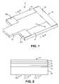
- FIG. 1is an isometric view of a PCB assembly according to the present invention
- FIG. 2is a cross-sectional view of a PCB forming a part of the PCB assembly shown in FIG. 1 taken along lines 2 — 2 in FIG. 1 ;
- FIG. 3is a top plan view of a first security trace layer forming a part of the PCB shown in FIG. 2 ;
- FIG. 4is a top plan view of a second security trace layer forming a part of the PCB shown in FIG. 2 ;
- FIG. 5is a top plan view of a secondary side layer forming a part of the PCB shown in FIG. 2 ;
- FIG. 6is a top plan view of a tamper wrap forming a part of the PCB assembly shown in FIG. 1 .
- the present inventionrelates to a PCB assembly, shown at reference numeral 5 , that includes a multilayer PCB 10 and a tamper wrap 15 that partially envelops PCB 10 .
- PCB 10is provided with electrical security elements that provide tamper protection in the areas of PCB 10 not covered by tamper wrap 15 . Together, these security elements and tamper wrap 15 provide a full envelope of tamper protection for all of the electrical components of PCB 10 .
- FIG. 2a cross-sectional diagram of PCB 10 taken along lines 2 — 2 in FIG. 1 is provided which shows each of the layers of PCB 10 .
- Each of the layers of PCB 10includes a substrate or base, made of, for example, fiberglass or glass epoxy, on which various elements are provided as described herein.
- PCB circuitry portion 20actually includes a number of layers, such as those included in a standard PCB, for example, a common six layer PCB.
- those layerspreferably include a primary layer on which electrical components 22 a – 2 c , such as, for example, integrated circuit chips, resistors, capacitors, and the like, are mounted, a ground plane layer, first, second and third signal layers, and a VCC plane layer.
- electrical components 22 a – 2 csuch as, for example, integrated circuit chips, resistors, capacitors, and the like
- ground plane layersuch as, for example, integrated circuit chips, resistors, capacitors, and the like
- first security trace layer 25 and second security trace layer 30are laminated on top of PCB circuitry portion 20 .
- FIGS. 3 and 4show representations of first security trace layer 25 and second security trace layer 30 , respectively.
- first security trace layer 25has provided thereon first and second serpentine traces 45 and 50 (only portions of which are illustrated in FIG. 3 for clarity) that preferably run adjacent to one another.
- second security trace layer 30has provided thereon first and second serpentine traces 55 and 60 (only portions of which are illustrated in FIG. 4 for clarity) that preferably run adjacent to one another.
- Serpentine traces 45 , 50 , 55 and 60are made of conductive material, and preferably made of copper, and are formed using conventional printed circuit board manufacturing methods.
- Serpentine trace 45is connected to serpentine trace 55 through a via 65
- serpentine trace 50is connected to serpentine trace 60 through a via 70
- serpentine traces 45 , 50 , 55 and 60are 5 mils wide or less, with 5 mils or less separating serpentine traces 45 and 50 on first security trace layer 25 and 5 mils or less separating serpentine traces 55 and 60 on second security trace layer 30 .
- the areas on first and second security trace layers 25 and 30 where serpentine traces 45 , 50 , 55 and 60 are routedextend across and cover substantially all of the surface of PCB 10 shown in FIG. 1 (with the exception of tab 75 ) that is not covered by tamper wrap 15 .
- serpentine traces 45 , 50 , 55 and 60 in combination with tamper wrap 15cover and restrict access to all of the electronics and electrical nodes provided on PCB 10 .
- serpentine traces 45 and 50 on first security trace layer 25are offset from serpentine traces 55 and 60 on second security trace layer 30 , most preferably by 5 mils or less, to ensure that there are no gaps in the area covered by serpentine traces 45 , 50 , 55 and 60 .
- serpentine traces 45 , 50 , 55 and 60are provided in offset patterns such that if security trace layer 25 is overlaid with security trace layer 30 , serpentine traces 45 and 50 will be aligned in between the gaps between serpentine traces 55 and 60 .
- serpentine traces 45 and 50were not offset from serpentine traces 55 and 60 (i.e., if they were lined up directly one on top of the other), a gap in coverage may be left that could be subject to probing or some other physical intrusion. It will be appreciated that while a serpentine shape is preferred, the traces provided on security trace layers 25 and 30 may take shapes other than a serpentine shape without departing from the scope of the present invention.
- serpentine trace 45is connected to tamper detection circuitry provided on PCB circuitry portion 20 through a via 80 .
- serpentine trace 50is connected to tamper detection circuitry provided on PCB circuitry portion 20 through a via 85 .
- the functionality of the tamper detection circuitry provided on PCB circuitry portion 20will be described in greater detail below.
- ground plane layer 35is laminated on top of second security trace layer 30 .
- Ground plane layer 35obscures from view the security traces, e.g., serpentine traces 45 , 50 , 55 and 60 , provided on first and second security trace layers 25 and 30 , thereby making it more difficult for an unauthorized person to avoid contact with the security traces while attempting to access the electronics provided on PCB circuitry portion 20 .
- PCB secondary side layer 40is laminated on top of ground plane layer 35 and is used to make electrical connections to tamper wrap 15 . Specifically, referring to FIGS.
- serpentine trace 55is connected to electrical contact 100 provided on PCB secondary side layer 40 through via 90
- serpentine trace 60is connected to electrical contact 105 provided on PCB secondary side layer 40 though via 95 .
- electrical contacts 100 and 105are used to make electrical connection to tamper wrap 15 when tamper wrap 15 is wrapped around PCB 10 as shown in FIG. 1 .
- FIG. 6is a top plan view of tamper wrap 15 , which is formed from a flexible film material.
- tamper wrap 15includes first side tab 16 opposite second side tab 17 and third side tab 18 opposite fourth side tabs 19 A and 19 B. Two fourth side tabs 19 A and 19 B are provided to accommodate tab 75 of PCB 10 . It will be appreciated that a single tab, similar to third side tab 18 , may be provided for PCBs that do not include tab 75 .
- Tamper wrap 15can include one or more layers of conductive material and insulating material. Tamper wrap 15 is also provided with first and second security traces 135 and 140 secured to the top surface and bottom surface, respectively of the tamper wrap 15 , preferably by an adhesive.
- the tracesare provided in a serpentine pattern, which may be random, pseudo-random or fixed, and cover at least a portion of each surface of the tamper wrap 15 , including the side tabs 16 , 17 , 18 , 19 a and 19 b.
- the first security trace 135located on the top surface of the tamper wrap 15 as illustrated in FIG. 6 , is connected at a first end thereof to electrical contact 110 and at a second end thereof to electrical contact 120 .
- second security trace 140located on the bottom surface of the tamper wrap 15 as illustrated in FIG. 6 , is connected at a first end thereof to electrical contact 115 and at a second end thereof to electrical contact 125 .
- electrical contact 110 of tamper wrap 15contacts electrical contact 100 of PCB secondary side layer 40
- electrical contact 115 of tamper wrap 15contacts electrical contact 105 of PCB secondary side layer 40
- electrical contact 120 of tamper wrap 15contacts electrical contact 175 of PCB secondary side layer 40
- electrical contact 125 of tamper wrap 15contacts electrical contact 180 of PCB secondary side layer 40 .
- Tamper wrap 15is attached to PCB 10 and held in place by an adhesive applied to the top surface of tamper wrap 15 .
- the adhesive property of this adhesiveis greater than the adhesive property of the adhesive used to secure the trace 135 to the tamper wrap 15 , such that security trace 135 will remain attached to the PCB 10 , thereby breaking and peeling away from tamper wrap 15 , should it be attempted to remove the tamper wrap 15 from the PCB 10 during a tamper attempt.
- electrical connection between the various electrical contacts as described aboveis preferably ensured using a conductive bonding agent, such as, for example, silver epoxy, applied between the electrical contacts during assembly.
- electrical contacts 175 and 180are each connected to tamper detection circuitry provided on PCB circuitry portion 20 through vias 185 and 190 , respectively.
- Tamper wrap 15when folded around PCB 10 as shown in FIG. 1 , covers not only the entire primary side of PCB 10 that includes PCB circuitry portion 20 (and the electronic components 22 a – 22 c mounted thereon), but also all of the vias that are used to make electrical connections (that are outside of the area covered by serpentine traces 45 , 50 , 55 and 60 ) and electrical contacts 100 , 105 , 110 , 115 , 120 , 125 , 180 and 185 .
- the first circuit pathbegins with the tamper detection circuitry provided on PCB circuitry portion 20 , continues through via 80 , serpentine trace 45 , via 65 , serpentine trace 55 , via 90 , electrical contact 100 , electrical contact 110 , first security trace 135 , electrical contact 120 , electrical contact 175 , and via 185 , and ends back at the tamper detection circuitry provided on PCB circuitry portion 20 .
- the second circuit pathbegins with the tamper detection circuitry provided on PCB circuitry portion 20 , continues through via 85 , serpentine trace 50 , via 70 , serpentine trace 60 , via 95 , electrical contact 105 , electrical contact 115 , second security trace 140 , electrical contact 125 , electrical contact 180 , and via 190 , and ends back at the tamper detection circuitry provided on PCB circuitry portion 20 .
- the tamper detection circuitryby monitoring these two circuit paths, is able to detect attempted unauthorized intrusions into PCB assembly 5 either through tamper wrap 15 or through the “security screen” provided by serpentine traces 45 , 50 , 55 and 60 .
- the two circuit pathscontinuously conduct current, provided by the tamper detection circuitry, and the tamper detection circuitry monitors the circuit paths for broken traces or shorts created when separate traces contact one another, each of which will indicate a tamper event resulting in some action taken by the tamper detection circuitry, such as zeroing encryption keys or deleting data.
- tamper wrap 15provides a first tamper protection portion that protects the electronics and electrical nodes of PCB 10 from tampering in all areas that tamper wrap 15 covers.
- the serpentine traces 45 , 50 , 55 and 60 provided on first security trace layer 25 and second security trace layer 30provide a second tamper protection portion in the form of a “security screen” that protects the electronics and electrical nodes of PCB 10 from tampering in the areas that they cover (and that are not covered by tamper wrap 15 ).
- PCB assembly 5is provided with a full tamper envelope that protects all electrical nodes forming a part of PCB 10 using only a partially enveloping tamper wrap 15 (tamper wrap 15 covers the entire top and sides of PCB 10 , but only a portion of the bottom of PCB 10 ), thereby reducing cost.
- tamper wrap 15covers the entire top and sides of PCB 10 , but only a portion of the bottom of PCB 10 ), thereby reducing cost.
- the need for manual soldering and potting as in prior art methodsis eliminated, thereby simplifying the overall manufacturing process.
Landscapes
- Engineering & Computer Science (AREA)
- Computer Hardware Design (AREA)
- Microelectronics & Electronic Packaging (AREA)
- General Physics & Mathematics (AREA)
- Computer Security & Cryptography (AREA)
- Theoretical Computer Science (AREA)
- Physics & Mathematics (AREA)
- General Engineering & Computer Science (AREA)
- Software Systems (AREA)
- Condensed Matter Physics & Semiconductors (AREA)
- Power Engineering (AREA)
- Pinball Game Machines (AREA)
- Transmitters (AREA)
- Structure Of Printed Boards (AREA)
Abstract
Description
Claims (12)
Priority Applications (4)
| Application Number | Priority Date | Filing Date | Title |
|---|---|---|---|
| US10/868,337US7180008B2 (en) | 2004-01-23 | 2004-06-15 | Tamper barrier for electronic device |
| DE602005025267TDE602005025267D1 (en) | 2004-01-23 | 2005-01-21 | Counterfeit barrier for electronic device |
| EP05001196AEP1557736B1 (en) | 2004-01-23 | 2005-01-21 | Tamper barrier for electronic device |
| US11/651,817US7475474B2 (en) | 2004-01-23 | 2007-01-10 | Method of making tamper detection circuit for an electronic device |
Applications Claiming Priority (2)
| Application Number | Priority Date | Filing Date | Title |
|---|---|---|---|
| US53855404P | 2004-01-23 | 2004-01-23 | |
| US10/868,337US7180008B2 (en) | 2004-01-23 | 2004-06-15 | Tamper barrier for electronic device |
Related Child Applications (1)
| Application Number | Title | Priority Date | Filing Date |
|---|---|---|---|
| US11/651,817DivisionUS7475474B2 (en) | 2004-01-23 | 2007-01-10 | Method of making tamper detection circuit for an electronic device |
Publications (2)
| Publication Number | Publication Date |
|---|---|
| US20050161253A1 US20050161253A1 (en) | 2005-07-28 |
| US7180008B2true US7180008B2 (en) | 2007-02-20 |
Family
ID=34636698
Family Applications (2)
| Application Number | Title | Priority Date | Filing Date |
|---|---|---|---|
| US10/868,337Expired - LifetimeUS7180008B2 (en) | 2004-01-23 | 2004-06-15 | Tamper barrier for electronic device |
| US11/651,817Expired - Fee RelatedUS7475474B2 (en) | 2004-01-23 | 2007-01-10 | Method of making tamper detection circuit for an electronic device |
Family Applications After (1)
| Application Number | Title | Priority Date | Filing Date |
|---|---|---|---|
| US11/651,817Expired - Fee RelatedUS7475474B2 (en) | 2004-01-23 | 2007-01-10 | Method of making tamper detection circuit for an electronic device |
Country Status (3)
| Country | Link |
|---|---|
| US (2) | US7180008B2 (en) |
| EP (1) | EP1557736B1 (en) |
| DE (1) | DE602005025267D1 (en) |
Cited By (49)
| Publication number | Priority date | Publication date | Assignee | Title |
|---|---|---|---|---|
| US20060080348A1 (en)* | 2000-11-20 | 2006-04-13 | International Business Machines Corporation | Security cloth design and assembly |
| US20070157682A1 (en)* | 2006-01-11 | 2007-07-12 | Honeywell International Inc. | Clamshell protective encasement |
| US20090070887A1 (en)* | 2007-09-06 | 2009-03-12 | Knowles Gareth J | Integrated laser Auto-Destruct System for Electronic Components |
| US20090146267A1 (en)* | 2007-12-05 | 2009-06-11 | Atmel Corporation | Secure connector grid array package |
| US20110090658A1 (en)* | 2009-10-14 | 2011-04-21 | Lockheed Martin Corporation | Protective circuit board cover |
| US7947911B1 (en)* | 2005-10-18 | 2011-05-24 | Teledyne Technologies Incorporated | Anti-tamper mesh |
| US20120050998A1 (en)* | 2011-11-03 | 2012-03-01 | Cram Worldwide, Llc | Heat dissipation for a chip protected by an anti-tamper background |
| DE102010048036A1 (en) | 2010-05-14 | 2012-08-30 | Häusermann GmbH | Printed circuit board for use in electronic device, such as medical device or electronic component, has one or multiple wiring layers and protection device |
| US20130241014A1 (en)* | 2012-03-13 | 2013-09-19 | Honeywell International Inc. | Magnetoresistive random access memory (mram) package including a multilayer magnetic security structure |
| US8854870B2 (en) | 2012-03-13 | 2014-10-07 | Honeywell International Inc. | Magnetoresistive random access memory (MRAM) die including an integrated magnetic security structure |
| US8896086B1 (en)* | 2013-05-30 | 2014-11-25 | Freescale Semiconductor, Inc. | System for preventing tampering with integrated circuit |
| US20150163933A1 (en)* | 2013-12-09 | 2015-06-11 | Timothy Wayne Steiner | Tamper respondent apparatus |
| US9418250B2 (en) | 2014-07-23 | 2016-08-16 | Freescale Semiconductor, Inc. | Tamper detector with hardware-based random number generator |
| US9419614B2 (en) | 2015-01-16 | 2016-08-16 | Freescale Semiconductor, Inc. | Low-power open-circuit detection system |
| US9455233B1 (en) | 2015-12-02 | 2016-09-27 | Freescale Semiconductor, Inc. | System for preventing tampering with integrated circuit |
| WO2016167750A1 (en)* | 2015-04-14 | 2016-10-20 | Hewlett Packard Enterprise Development Lp | Penetration detection boundary having a heat sink |
| US9554477B1 (en) | 2015-12-18 | 2017-01-24 | International Business Machines Corporation | Tamper-respondent assemblies with enclosure-to-board protection |
| US9560737B2 (en) | 2015-03-04 | 2017-01-31 | International Business Machines Corporation | Electronic package with heat transfer element(s) |
| US9555606B1 (en) | 2015-12-09 | 2017-01-31 | International Business Machines Corporation | Applying pressure to adhesive using CTE mismatch between components |
| US9578764B1 (en) | 2015-09-25 | 2017-02-21 | International Business Machines Corporation | Enclosure with inner tamper-respondent sensor(s) and physical security element(s) |
| US9591776B1 (en) | 2015-09-25 | 2017-03-07 | International Business Machines Corporation | Enclosure with inner tamper-respondent sensor(s) |
| US9858776B1 (en) | 2016-06-28 | 2018-01-02 | International Business Machines Corporation | Tamper-respondent assembly with nonlinearity monitoring |
| US9881880B2 (en) | 2016-05-13 | 2018-01-30 | International Business Machines Corporation | Tamper-proof electronic packages with stressed glass component substrate(s) |
| US9894749B2 (en) | 2015-09-25 | 2018-02-13 | International Business Machines Corporation | Tamper-respondent assemblies with bond protection |
| US9904811B2 (en) | 2016-04-27 | 2018-02-27 | International Business Machines Corporation | Tamper-proof electronic packages with two-phase dielectric fluid |
| US20180061196A1 (en)* | 2016-02-25 | 2018-03-01 | International Business Machines Corporation | Multi-layer stack with embedded tamper-detect protection |
| US9911012B2 (en) | 2015-09-25 | 2018-03-06 | International Business Machines Corporation | Overlapping, discrete tamper-respondent sensors |
| US9913370B2 (en) | 2016-05-13 | 2018-03-06 | International Business Machines Corporation | Tamper-proof electronic packages formed with stressed glass |
| US9913389B2 (en) | 2015-12-01 | 2018-03-06 | International Business Corporation Corporation | Tamper-respondent assembly with vent structure |
| US9924591B2 (en) | 2015-09-25 | 2018-03-20 | International Business Machines Corporation | Tamper-respondent assemblies |
| US9978231B2 (en) | 2015-10-21 | 2018-05-22 | International Business Machines Corporation | Tamper-respondent assembly with protective wrap(s) over tamper-respondent sensor(s) |
| US9999124B2 (en) | 2016-11-02 | 2018-06-12 | International Business Machines Corporation | Tamper-respondent assemblies with trace regions of increased susceptibility to breaking |
| US10098235B2 (en) | 2015-09-25 | 2018-10-09 | International Business Machines Corporation | Tamper-respondent assemblies with region(s) of increased susceptibility to damage |
| US10136519B2 (en) | 2015-10-19 | 2018-11-20 | International Business Machines Corporation | Circuit layouts of tamper-respondent sensors |
| US10168185B2 (en) | 2015-09-25 | 2019-01-01 | International Business Machines Corporation | Circuit boards and electronic packages with embedded tamper-respondent sensor |
| US10172239B2 (en) | 2015-09-25 | 2019-01-01 | International Business Machines Corporation | Tamper-respondent sensors with formed flexible layer(s) |
| US10271424B2 (en) | 2016-09-26 | 2019-04-23 | International Business Machines Corporation | Tamper-respondent assemblies with in situ vent structure(s) |
| EP3478032A1 (en) | 2017-10-24 | 2019-05-01 | VARTA Microbattery GmbH | Circuit board and use of an edge protection profile |
| US10299372B2 (en) | 2016-09-26 | 2019-05-21 | International Business Machines Corporation | Vented tamper-respondent assemblies |
| US10306753B1 (en) | 2018-02-22 | 2019-05-28 | International Business Machines Corporation | Enclosure-to-board interface with tamper-detect circuit(s) |
| US10312625B2 (en)* | 2017-01-13 | 2019-06-04 | Ingenico Group | Secured body for memory card reader |
| US10321589B2 (en)* | 2016-09-19 | 2019-06-11 | International Business Machines Corporation | Tamper-respondent assembly with sensor connection adapter |
| US10327343B2 (en) | 2015-12-09 | 2019-06-18 | International Business Machines Corporation | Applying pressure to adhesive using CTE mismatch between components |
| US10327329B2 (en) | 2017-02-13 | 2019-06-18 | International Business Machines Corporation | Tamper-respondent assembly with flexible tamper-detect sensor(s) overlying in-situ-formed tamper-detect sensor |
| US10426037B2 (en) | 2015-07-15 | 2019-09-24 | International Business Machines Corporation | Circuitized structure with 3-dimensional configuration |
| US10579833B1 (en) | 2014-12-16 | 2020-03-03 | Thales Esecurity, Inc. | Tamper detection circuit assemblies and related manufacturing processes |
| US10740499B2 (en) | 2018-03-12 | 2020-08-11 | Nuvoton Technology Corporation | Active shield portion serving as serial keypad |
| US10938841B2 (en) | 2017-11-02 | 2021-03-02 | Raytheon Company | Multi-GHz guard sensor for detecting physical or electromagnetic intrusions of a guarded region |
| US11122682B2 (en) | 2018-04-04 | 2021-09-14 | International Business Machines Corporation | Tamper-respondent sensors with liquid crystal polymer layers |
Families Citing this family (23)
| Publication number | Priority date | Publication date | Assignee | Title |
|---|---|---|---|---|
| IL171963A0 (en) | 2005-11-14 | 2006-04-10 | Nds Ltd | Secure read-write storage device |
| ITFI20060077A1 (en) | 2006-03-23 | 2007-09-24 | Gilbarco S P A | DEVICE FOR VERIFYING THE REGULARITY OF THE OPERATION OF AUTOMATIC PAYMENT TERMINALS |
| SG137706A1 (en)* | 2006-05-11 | 2007-12-28 | Chng Weng Wah | Theft-deterrent mechanism and method and retail packaging employed the same |
| US7915540B2 (en)* | 2006-06-09 | 2011-03-29 | International Business Machines Corporation | Tamper-proof structures for protecting electronic modules |
| DE102006027682B3 (en)* | 2006-06-14 | 2008-01-31 | Infineon Technologies Ag | Integrated circuit arrangement and method for operating an integrated circuit arrangement |
| DE102007046026A1 (en)* | 2007-09-26 | 2009-04-02 | Rohde & Schwarz Sit Gmbh | Protective arrangement and manufacturing method for a protective device |
| US20090307140A1 (en)* | 2008-06-06 | 2009-12-10 | Upendra Mardikar | Mobile device over-the-air (ota) registration and point-of-sale (pos) payment |
| US20100123469A1 (en)* | 2008-11-19 | 2010-05-20 | Edward Craig Hyatt | System and method for protecting circuit boards |
| US20110080715A1 (en)* | 2009-10-07 | 2011-04-07 | Castles Technology Co., Ltd. | Protective structure of electronic component |
| JP2012053788A (en)* | 2010-09-02 | 2012-03-15 | Canon Inc | Semiconductor integrated circuit device |
| US8719957B2 (en)* | 2011-04-29 | 2014-05-06 | Altera Corporation | Systems and methods for detecting and mitigating programmable logic device tampering |
| US8862767B2 (en) | 2011-09-02 | 2014-10-14 | Ebay Inc. | Secure elements broker (SEB) for application communication channel selector optimization |
| GB2505178A (en)* | 2012-08-20 | 2014-02-26 | Johnson Electric Sa | Stackable Overlapping Security Wrap Film for Protecting Electronic Device. |
| WO2014086987A2 (en) | 2012-12-07 | 2014-06-12 | Cryptera A/S | A security module for protecting circuit components from unauthorized access |
| US9226392B2 (en)* | 2013-01-18 | 2015-12-29 | Xac Automation Corp. | Tamper protection device and data transaction apparatus |
| EP3019996B1 (en)* | 2013-07-11 | 2019-03-13 | Cryptera A/S | Tamper responsive sensor |
| US20160174388A1 (en) | 2014-12-15 | 2016-06-16 | International Business Machines Corporation | Printed circuit board security using embedded photodetector circuit |
| US9887847B2 (en) | 2016-02-03 | 2018-02-06 | International Business Machines Corporation | Secure crypto module including conductor on glass security layer |
| WO2018104890A2 (en) | 2016-12-06 | 2018-06-14 | Enrico Maim | Methods and entities, in particular of a transactional nature, using secure devices |
| EP3710970B1 (en) | 2017-11-15 | 2024-05-15 | Enrico Maim | Terminals and methods for secure transactions |
| US10157527B1 (en)* | 2017-11-28 | 2018-12-18 | International Business Machines Corporation | Embossed printed circuit board for intrusion detection |
| US11341286B2 (en) | 2018-10-22 | 2022-05-24 | TE Connectivity Services Gmbh | Tamper sensor assembly |
| US11270032B1 (en) | 2018-12-27 | 2022-03-08 | Thales E-Security, Inc. | Tamper switch assembly and installation method thereof |
Citations (50)
| Publication number | Priority date | Publication date | Assignee | Title |
|---|---|---|---|---|
| US4160503A (en) | 1978-08-07 | 1979-07-10 | Ohlbach Ralph C | Shipping container for printed circuit boards and other items |
| US4211324A (en) | 1978-08-07 | 1980-07-08 | Ohlbach Ralph C | Assembly protecting and inventorying printed circuit boards |
| US4516679A (en) | 1982-11-04 | 1985-05-14 | Simpson Carolyn N | Tamper-proof wrap |
| US4593384A (en) | 1984-12-21 | 1986-06-03 | Ncr Corporation | Security device for the secure storage of sensitive data |
| US4609104A (en) | 1985-06-04 | 1986-09-02 | Ade, Inc. | RFI shielded, multiple part container and components thereof |
| GB2174830A (en) | 1985-04-27 | 1986-11-12 | David Clark | Tamper-proof enclosures |
| US4653252A (en) | 1984-01-19 | 1987-03-31 | Douwe Egberts Koninklijke Tabaksfabriek Koffiebranderijen-Theehandel N.V. | Packing method and a blank for use therein |
| US4677809A (en) | 1985-05-10 | 1987-07-07 | General Dyanmics, Pomona Division | Method of making packing material with anti-static coating |
| US4691350A (en) | 1985-10-30 | 1987-09-01 | Ncr Corporation | Security device for stored sensitive data |
| US4807284A (en) | 1986-09-24 | 1989-02-21 | Ncr Corporation | Security device for sensitive data |
| US4811288A (en) | 1985-09-25 | 1989-03-07 | Ncr Corporation | Data security device for protecting stored data |
| US4860351A (en) | 1986-11-05 | 1989-08-22 | Ibm Corporation | Tamper-resistant packaging for protection of information stored in electronic circuitry |
| US4865197A (en) | 1988-03-04 | 1989-09-12 | Unisys Corporation | Electronic component transportation container |
| US5009311A (en) | 1990-06-11 | 1991-04-23 | Schenk Robert J | Removable rigid support structure for circuit cards |
| US5075822A (en) | 1989-03-04 | 1991-12-24 | Telefunken Electronic Gmbh | Housing for installation in motor vehicles |
| US5117457A (en) | 1986-11-05 | 1992-05-26 | International Business Machines Corp. | Tamper resistant packaging for information protection in electronic circuitry |
| US5201868A (en) | 1991-01-22 | 1993-04-13 | Rock-Tenn Company | Insulated shipping container |
| US5211618A (en) | 1992-08-03 | 1993-05-18 | The Mead Corporation | Self-centering laminated process for corrugated containers and blank therefor |
| EP0629497A2 (en) | 1993-06-03 | 1994-12-21 | Trigon Industries Limited | A multi-wall film |
| US5389738A (en) | 1992-05-04 | 1995-02-14 | Motorola, Inc. | Tamperproof arrangement for an integrated circuit device |
| GB2297540A (en) | 1993-03-12 | 1996-08-07 | Gore & Ass | Tamper respondent enclosure |
| GB2298391A (en) | 1995-03-02 | 1996-09-04 | De La Rue Holographics Ltd | Tamper Indicating Security Item |
| US5675319A (en) | 1996-04-26 | 1997-10-07 | David Sarnoff Research Center, Inc. | Tamper detection device |
| US5715652A (en) | 1994-11-18 | 1998-02-10 | Ruediger Haaga Gmbh | Apparatus for producing and applying a protective covering to a cut edge of an opening of a container wall |
| US5880523A (en) | 1997-02-24 | 1999-03-09 | General Instrument Corporation | Anti-tamper integrated circuit |
| GB2330439A (en) | 1997-10-17 | 1999-04-21 | Gore & Ass | Tamper respondent enclosure |
| WO1999021142A1 (en) | 1997-10-17 | 1999-04-29 | W. L. Gore & Associates (Uk) Limited | Tamper respondent enclosure |
| DE19816572A1 (en) | 1998-04-07 | 1999-10-14 | Francotyp Postalia Gmbh | Security module to prevent manipulation of data |
| DE19816571A1 (en) | 1998-04-07 | 1999-10-14 | Francotyp Postalia Gmbh | Access protection for security modules |
| US5988510A (en) | 1997-02-13 | 1999-11-23 | Micron Communications, Inc. | Tamper resistant smart card and method of protecting data in a smart card |
| US6121544A (en) | 1998-01-15 | 2000-09-19 | Petsinger; Julie Ann | Electromagnetic shield to prevent surreptitious access to contactless smartcards |
| US6195267B1 (en) | 1999-06-23 | 2001-02-27 | Ericsson Inc. | Gel structure for combined EMI shielding and thermal control of microelectronic assemblies |
| US6261215B1 (en) | 1996-03-21 | 2001-07-17 | Rodney Haydn Imer | Rectangular thin film pack |
| WO2001063994A2 (en) | 2000-02-23 | 2001-08-30 | Iridian Technologies, Inc. | Tamper proof case for electronic devices having memories with sensitive information |
| US20010056542A1 (en) | 2000-05-11 | 2001-12-27 | International Business Machines Corporation | Tamper resistant card enclosure with improved intrusion detection circuit |
| US20020002683A1 (en) | 2000-02-14 | 2002-01-03 | Benson Justin H. | Security module system, apparatus and process |
| EP1184773A1 (en) | 2000-09-01 | 2002-03-06 | International Business Machines Corporation | A method of securing an electronic assembly against tampering |
| EP1207444A2 (en) | 2000-11-20 | 2002-05-22 | International Business Machines Corporation | Security cloth design and assembly |
| US20020084090A1 (en) | 2001-01-03 | 2002-07-04 | Farquhar Donald S. | Tamper-responding encapsulated enclosure having flexible protective mesh structure |
| US6424954B1 (en) | 1998-02-17 | 2002-07-23 | Neopost Inc. | Postage metering system |
| US6469625B1 (en) | 2000-02-18 | 2002-10-22 | Optex Co., Ltd | Security sensor having disturbance detecting capability |
| US6473304B1 (en) | 1996-12-23 | 2002-10-29 | David Leonard Stevens | Thermally conductive case for electrical components and method of manufacture therefor |
| US6643995B1 (en) | 1999-05-24 | 2003-11-11 | Uni-Charm Corporation | Process and apparatus for manufacturing packages |
| US6853093B2 (en)* | 2002-12-20 | 2005-02-08 | Lipman Electronic Engineering Ltd. | Anti-tampering enclosure for electronic circuitry |
| US6970360B2 (en)* | 2004-03-18 | 2005-11-29 | International Business Machines Corporation | Tamper-proof enclosure for a circuit card |
| US6985362B2 (en) | 2000-09-07 | 2006-01-10 | International Business Machines Corporation | Printed circuit board and electronic package using same |
| US6996953B2 (en) | 2004-01-23 | 2006-02-14 | Pitney Bowes Inc. | System and method for installing a tamper barrier wrap in a PCB assembly, including a PCB assembly having improved heat sinking |
| US7015823B1 (en)* | 2004-10-15 | 2006-03-21 | Systran Federal Corporation | Tamper resistant circuit boards |
| US7057896B2 (en)* | 2002-08-21 | 2006-06-06 | Matsushita Electric Industrial Co., Ltd. | Power module and production method thereof |
| US7095615B2 (en)* | 2003-11-13 | 2006-08-22 | Honeywell International, Inc. | Environmentally tuned circuit card assembly and method for manufacturing the same |
Family Cites Families (6)
| Publication number | Priority date | Publication date | Assignee | Title |
|---|---|---|---|---|
| US5185717A (en)* | 1988-08-05 | 1993-02-09 | Ryoichi Mori | Tamper resistant module having logical elements arranged in multiple layers on the outer surface of a substrate to protect stored information |
| US5239664A (en)* | 1988-12-20 | 1993-08-24 | Bull S.A. | Arrangement for protecting an electronic card and its use for protecting a terminal for reading magnetic and/or microprocessor cards |
| US5027397A (en)* | 1989-09-12 | 1991-06-25 | International Business Machines Corporation | Data protection by detection of intrusion into electronic assemblies |
| US5195267A (en)* | 1991-10-08 | 1993-03-23 | Daniels John J | Tension responsive fishing apparatus |
| TW471144B (en)* | 1995-03-28 | 2002-01-01 | Intel Corp | Method to prevent intrusions into electronic circuitry |
| DE19639033C1 (en)* | 1996-09-23 | 1997-08-07 | Siemens Ag | Copy prevention arrangement for semiconductor chip |
- 2004
- 2004-06-15USUS10/868,337patent/US7180008B2/ennot_activeExpired - Lifetime
- 2005
- 2005-01-21EPEP05001196Apatent/EP1557736B1/ennot_activeExpired - Lifetime
- 2005-01-21DEDE602005025267Tpatent/DE602005025267D1/ennot_activeExpired - Lifetime
- 2007
- 2007-01-10USUS11/651,817patent/US7475474B2/ennot_activeExpired - Fee Related
Patent Citations (55)
| Publication number | Priority date | Publication date | Assignee | Title |
|---|---|---|---|---|
| US4211324A (en) | 1978-08-07 | 1980-07-08 | Ohlbach Ralph C | Assembly protecting and inventorying printed circuit boards |
| US4160503A (en) | 1978-08-07 | 1979-07-10 | Ohlbach Ralph C | Shipping container for printed circuit boards and other items |
| US4516679A (en) | 1982-11-04 | 1985-05-14 | Simpson Carolyn N | Tamper-proof wrap |
| US4653252A (en) | 1984-01-19 | 1987-03-31 | Douwe Egberts Koninklijke Tabaksfabriek Koffiebranderijen-Theehandel N.V. | Packing method and a blank for use therein |
| US4593384A (en) | 1984-12-21 | 1986-06-03 | Ncr Corporation | Security device for the secure storage of sensitive data |
| GB2174830A (en) | 1985-04-27 | 1986-11-12 | David Clark | Tamper-proof enclosures |
| US4677809A (en) | 1985-05-10 | 1987-07-07 | General Dyanmics, Pomona Division | Method of making packing material with anti-static coating |
| US4609104A (en) | 1985-06-04 | 1986-09-02 | Ade, Inc. | RFI shielded, multiple part container and components thereof |
| US4811288A (en) | 1985-09-25 | 1989-03-07 | Ncr Corporation | Data security device for protecting stored data |
| US4691350A (en) | 1985-10-30 | 1987-09-01 | Ncr Corporation | Security device for stored sensitive data |
| US4807284A (en) | 1986-09-24 | 1989-02-21 | Ncr Corporation | Security device for sensitive data |
| US4860351A (en) | 1986-11-05 | 1989-08-22 | Ibm Corporation | Tamper-resistant packaging for protection of information stored in electronic circuitry |
| US5117457A (en) | 1986-11-05 | 1992-05-26 | International Business Machines Corp. | Tamper resistant packaging for information protection in electronic circuitry |
| US4865197A (en) | 1988-03-04 | 1989-09-12 | Unisys Corporation | Electronic component transportation container |
| US5075822A (en) | 1989-03-04 | 1991-12-24 | Telefunken Electronic Gmbh | Housing for installation in motor vehicles |
| US5009311A (en) | 1990-06-11 | 1991-04-23 | Schenk Robert J | Removable rigid support structure for circuit cards |
| US5201868A (en) | 1991-01-22 | 1993-04-13 | Rock-Tenn Company | Insulated shipping container |
| US5389738A (en) | 1992-05-04 | 1995-02-14 | Motorola, Inc. | Tamperproof arrangement for an integrated circuit device |
| US5406630A (en) | 1992-05-04 | 1995-04-11 | Motorola, Inc. | Tamperproof arrangement for an integrated circuit device |
| US5211618A (en) | 1992-08-03 | 1993-05-18 | The Mead Corporation | Self-centering laminated process for corrugated containers and blank therefor |
| US5858500A (en) | 1993-03-12 | 1999-01-12 | W. L. Gore & Associates, Inc. | Tamper respondent enclosure |
| GB2297540A (en) | 1993-03-12 | 1996-08-07 | Gore & Ass | Tamper respondent enclosure |
| EP0629497A2 (en) | 1993-06-03 | 1994-12-21 | Trigon Industries Limited | A multi-wall film |
| US5715652A (en) | 1994-11-18 | 1998-02-10 | Ruediger Haaga Gmbh | Apparatus for producing and applying a protective covering to a cut edge of an opening of a container wall |
| GB2298391A (en) | 1995-03-02 | 1996-09-04 | De La Rue Holographics Ltd | Tamper Indicating Security Item |
| US6261215B1 (en) | 1996-03-21 | 2001-07-17 | Rodney Haydn Imer | Rectangular thin film pack |
| US5675319A (en) | 1996-04-26 | 1997-10-07 | David Sarnoff Research Center, Inc. | Tamper detection device |
| US6473304B1 (en) | 1996-12-23 | 2002-10-29 | David Leonard Stevens | Thermally conductive case for electrical components and method of manufacture therefor |
| US5988510A (en) | 1997-02-13 | 1999-11-23 | Micron Communications, Inc. | Tamper resistant smart card and method of protecting data in a smart card |
| US5880523A (en) | 1997-02-24 | 1999-03-09 | General Instrument Corporation | Anti-tamper integrated circuit |
| WO1999021142A1 (en) | 1997-10-17 | 1999-04-29 | W. L. Gore & Associates (Uk) Limited | Tamper respondent enclosure |
| GB2330439A (en) | 1997-10-17 | 1999-04-21 | Gore & Ass | Tamper respondent enclosure |
| US6121544A (en) | 1998-01-15 | 2000-09-19 | Petsinger; Julie Ann | Electromagnetic shield to prevent surreptitious access to contactless smartcards |
| US6424954B1 (en) | 1998-02-17 | 2002-07-23 | Neopost Inc. | Postage metering system |
| DE19816572A1 (en) | 1998-04-07 | 1999-10-14 | Francotyp Postalia Gmbh | Security module to prevent manipulation of data |
| DE19816571A1 (en) | 1998-04-07 | 1999-10-14 | Francotyp Postalia Gmbh | Access protection for security modules |
| US6643995B1 (en) | 1999-05-24 | 2003-11-11 | Uni-Charm Corporation | Process and apparatus for manufacturing packages |
| US6195267B1 (en) | 1999-06-23 | 2001-02-27 | Ericsson Inc. | Gel structure for combined EMI shielding and thermal control of microelectronic assemblies |
| US20020002683A1 (en) | 2000-02-14 | 2002-01-03 | Benson Justin H. | Security module system, apparatus and process |
| US7054162B2 (en)* | 2000-02-14 | 2006-05-30 | Safenet, Inc. | Security module system, apparatus and process |
| US6469625B1 (en) | 2000-02-18 | 2002-10-22 | Optex Co., Ltd | Security sensor having disturbance detecting capability |
| WO2001063994A2 (en) | 2000-02-23 | 2001-08-30 | Iridian Technologies, Inc. | Tamper proof case for electronic devices having memories with sensitive information |
| US20010056542A1 (en) | 2000-05-11 | 2001-12-27 | International Business Machines Corporation | Tamper resistant card enclosure with improved intrusion detection circuit |
| EP1184773A1 (en) | 2000-09-01 | 2002-03-06 | International Business Machines Corporation | A method of securing an electronic assembly against tampering |
| US6985362B2 (en) | 2000-09-07 | 2006-01-10 | International Business Machines Corporation | Printed circuit board and electronic package using same |
| EP1207444A2 (en) | 2000-11-20 | 2002-05-22 | International Business Machines Corporation | Security cloth design and assembly |
| US20020084090A1 (en) | 2001-01-03 | 2002-07-04 | Farquhar Donald S. | Tamper-responding encapsulated enclosure having flexible protective mesh structure |
| US6686539B2 (en) | 2001-01-03 | 2004-02-03 | International Business Machines Corporation | Tamper-responding encapsulated enclosure having flexible protective mesh structure |
| US6929900B2 (en)* | 2001-01-03 | 2005-08-16 | International Business Machines Corporation | Tamper-responding encapsulated enclosure having flexible protective mesh structure |
| US7057896B2 (en)* | 2002-08-21 | 2006-06-06 | Matsushita Electric Industrial Co., Ltd. | Power module and production method thereof |
| US6853093B2 (en)* | 2002-12-20 | 2005-02-08 | Lipman Electronic Engineering Ltd. | Anti-tampering enclosure for electronic circuitry |
| US7095615B2 (en)* | 2003-11-13 | 2006-08-22 | Honeywell International, Inc. | Environmentally tuned circuit card assembly and method for manufacturing the same |
| US6996953B2 (en) | 2004-01-23 | 2006-02-14 | Pitney Bowes Inc. | System and method for installing a tamper barrier wrap in a PCB assembly, including a PCB assembly having improved heat sinking |
| US6970360B2 (en)* | 2004-03-18 | 2005-11-29 | International Business Machines Corporation | Tamper-proof enclosure for a circuit card |
| US7015823B1 (en)* | 2004-10-15 | 2006-03-21 | Systran Federal Corporation | Tamper resistant circuit boards |
Non-Patent Citations (1)
| Title |
|---|
| FIPS PUB 140-2 Federal Information Processing Standards Publication-Security Requirements for Cryptographic Modules, Issued May 25, 2001. |
Cited By (97)
| Publication number | Priority date | Publication date | Assignee | Title |
|---|---|---|---|---|
| US7679921B2 (en)* | 2000-11-20 | 2010-03-16 | International Business Machines Corporation | Security cloth design and assembly |
| US20060080348A1 (en)* | 2000-11-20 | 2006-04-13 | International Business Machines Corporation | Security cloth design and assembly |
| US7947911B1 (en)* | 2005-10-18 | 2011-05-24 | Teledyne Technologies Incorporated | Anti-tamper mesh |
| US8399781B1 (en) | 2005-10-18 | 2013-03-19 | Teledyne Technologies Incorporated | Anti-tamper mesh |
| US20070157682A1 (en)* | 2006-01-11 | 2007-07-12 | Honeywell International Inc. | Clamshell protective encasement |
| US7495554B2 (en)* | 2006-01-11 | 2009-02-24 | Honeywell International Inc. | Clamshell protective encasement |
| US20090070887A1 (en)* | 2007-09-06 | 2009-03-12 | Knowles Gareth J | Integrated laser Auto-Destruct System for Electronic Components |
| US9704817B2 (en) | 2007-09-06 | 2017-07-11 | Qortek, Inc. | Integrated laser auto-destruct system for electronic components |
| US7812428B2 (en) | 2007-12-05 | 2010-10-12 | Atmel Rousset S.A.S. | Secure connector grid array package |
| US20090146267A1 (en)* | 2007-12-05 | 2009-06-11 | Atmel Corporation | Secure connector grid array package |
| US20110090658A1 (en)* | 2009-10-14 | 2011-04-21 | Lockheed Martin Corporation | Protective circuit board cover |
| US8659908B2 (en)* | 2009-10-14 | 2014-02-25 | Lockheed Martin Corporation | Protective circuit board cover |
| DE102010048036A1 (en) | 2010-05-14 | 2012-08-30 | Häusermann GmbH | Printed circuit board for use in electronic device, such as medical device or electronic component, has one or multiple wiring layers and protection device |
| US20120050998A1 (en)* | 2011-11-03 | 2012-03-01 | Cram Worldwide, Llc | Heat dissipation for a chip protected by an anti-tamper background |
| US9066447B2 (en)* | 2011-11-03 | 2015-06-23 | Cram Worldwide, Llc | Heat dissipation for a chip protected by an anti-tamper background |
| US8811072B2 (en)* | 2012-03-13 | 2014-08-19 | Honeywell International Inc. | Magnetoresistive random access memory (MRAM) package including a multilayer magnetic security structure |
| US8854870B2 (en) | 2012-03-13 | 2014-10-07 | Honeywell International Inc. | Magnetoresistive random access memory (MRAM) die including an integrated magnetic security structure |
| US20130241014A1 (en)* | 2012-03-13 | 2013-09-19 | Honeywell International Inc. | Magnetoresistive random access memory (mram) package including a multilayer magnetic security structure |
| US20140353849A1 (en)* | 2013-05-30 | 2014-12-04 | Mohit Arora | System for preventing tampering with integrated circuit |
| US8896086B1 (en)* | 2013-05-30 | 2014-11-25 | Freescale Semiconductor, Inc. | System for preventing tampering with integrated circuit |
| US9521764B2 (en)* | 2013-12-09 | 2016-12-13 | Timothy Steiner | Tamper respondent apparatus |
| US20150163933A1 (en)* | 2013-12-09 | 2015-06-11 | Timothy Wayne Steiner | Tamper respondent apparatus |
| US9418250B2 (en) | 2014-07-23 | 2016-08-16 | Freescale Semiconductor, Inc. | Tamper detector with hardware-based random number generator |
| US11250171B1 (en) | 2014-12-16 | 2022-02-15 | Thales Esecurity, Inc. | Three-dimensional (3D) printing of a tamper sensor assembly |
| US10579833B1 (en) | 2014-12-16 | 2020-03-03 | Thales Esecurity, Inc. | Tamper detection circuit assemblies and related manufacturing processes |
| US9419614B2 (en) | 2015-01-16 | 2016-08-16 | Freescale Semiconductor, Inc. | Low-power open-circuit detection system |
| US10237964B2 (en) | 2015-03-04 | 2019-03-19 | International Business Machines Corporation | Manufacturing electronic package with heat transfer element(s) |
| US9560737B2 (en) | 2015-03-04 | 2017-01-31 | International Business Machines Corporation | Electronic package with heat transfer element(s) |
| WO2016167750A1 (en)* | 2015-04-14 | 2016-10-20 | Hewlett Packard Enterprise Development Lp | Penetration detection boundary having a heat sink |
| US10426037B2 (en) | 2015-07-15 | 2019-09-24 | International Business Machines Corporation | Circuitized structure with 3-dimensional configuration |
| US10524362B2 (en) | 2015-07-15 | 2019-12-31 | International Business Machines Corporation | Circuitized structure with 3-dimensional configuration |
| US9578764B1 (en) | 2015-09-25 | 2017-02-21 | International Business Machines Corporation | Enclosure with inner tamper-respondent sensor(s) and physical security element(s) |
| US10271434B2 (en) | 2015-09-25 | 2019-04-23 | International Business Machines Corporation | Method of fabricating a tamper-respondent assembly with region(s) of increased susceptibility to damage |
| US9591776B1 (en) | 2015-09-25 | 2017-03-07 | International Business Machines Corporation | Enclosure with inner tamper-respondent sensor(s) |
| US10172239B2 (en) | 2015-09-25 | 2019-01-01 | International Business Machines Corporation | Tamper-respondent sensors with formed flexible layer(s) |
| US10395067B2 (en) | 2015-09-25 | 2019-08-27 | International Business Machines Corporation | Method of fabricating a tamper-respondent sensor assembly |
| US9894749B2 (en) | 2015-09-25 | 2018-02-13 | International Business Machines Corporation | Tamper-respondent assemblies with bond protection |
| US10378924B2 (en) | 2015-09-25 | 2019-08-13 | International Business Machines Corporation | Circuit boards and electronic packages with embedded tamper-respondent sensor |
| US10378925B2 (en) | 2015-09-25 | 2019-08-13 | International Business Machines Corporation | Circuit boards and electronic packages with embedded tamper-respondent sensor |
| US9911012B2 (en) | 2015-09-25 | 2018-03-06 | International Business Machines Corporation | Overlapping, discrete tamper-respondent sensors |
| US10334722B2 (en) | 2015-09-25 | 2019-06-25 | International Business Machines Corporation | Tamper-respondent assemblies |
| US9913416B2 (en) | 2015-09-25 | 2018-03-06 | International Business Machines Corporation | Enclosure with inner tamper-respondent sensor(s) and physical security element(s) |
| US9913362B2 (en) | 2015-09-25 | 2018-03-06 | International Business Machines Corporation | Tamper-respondent assemblies with bond protection |
| US10331915B2 (en) | 2015-09-25 | 2019-06-25 | International Business Machines Corporation | Overlapping, discrete tamper-respondent sensors |
| US9717154B2 (en) | 2015-09-25 | 2017-07-25 | International Business Machines Corporation | Enclosure with inner tamper-respondent sensor(s) |
| US9924591B2 (en) | 2015-09-25 | 2018-03-20 | International Business Machines Corporation | Tamper-respondent assemblies |
| US9936573B2 (en) | 2015-09-25 | 2018-04-03 | International Business Machines Corporation | Tamper-respondent assemblies |
| US10624202B2 (en) | 2015-09-25 | 2020-04-14 | International Business Machines Corporation | Tamper-respondent assemblies with bond protection |
| US10264665B2 (en) | 2015-09-25 | 2019-04-16 | International Business Machines Corporation | Tamper-respondent assemblies with bond protection |
| US10098235B2 (en) | 2015-09-25 | 2018-10-09 | International Business Machines Corporation | Tamper-respondent assemblies with region(s) of increased susceptibility to damage |
| US10257939B2 (en) | 2015-09-25 | 2019-04-09 | International Business Machines Corporation | Method of fabricating tamper-respondent sensor |
| US10178818B2 (en) | 2015-09-25 | 2019-01-08 | International Business Machines Corporation | Enclosure with inner tamper-respondent sensor(s) and physical security element(s) |
| US10175064B2 (en) | 2015-09-25 | 2019-01-08 | International Business Machines Corporation | Circuit boards and electronic packages with embedded tamper-respondent sensor |
| US10168185B2 (en) | 2015-09-25 | 2019-01-01 | International Business Machines Corporation | Circuit boards and electronic packages with embedded tamper-respondent sensor |
| US10685146B2 (en) | 2015-09-25 | 2020-06-16 | International Business Machines Corporation | Overlapping, discrete tamper-respondent sensors |
| US10143090B2 (en) | 2015-10-19 | 2018-11-27 | International Business Machines Corporation | Circuit layouts of tamper-respondent sensors |
| US10136519B2 (en) | 2015-10-19 | 2018-11-20 | International Business Machines Corporation | Circuit layouts of tamper-respondent sensors |
| US9978231B2 (en) | 2015-10-21 | 2018-05-22 | International Business Machines Corporation | Tamper-respondent assembly with protective wrap(s) over tamper-respondent sensor(s) |
| US9913389B2 (en) | 2015-12-01 | 2018-03-06 | International Business Corporation Corporation | Tamper-respondent assembly with vent structure |
| US10251288B2 (en) | 2015-12-01 | 2019-04-02 | International Business Machines Corporation | Tamper-respondent assembly with vent structure |
| US9455233B1 (en) | 2015-12-02 | 2016-09-27 | Freescale Semiconductor, Inc. | System for preventing tampering with integrated circuit |
| US9555606B1 (en) | 2015-12-09 | 2017-01-31 | International Business Machines Corporation | Applying pressure to adhesive using CTE mismatch between components |
| US10327343B2 (en) | 2015-12-09 | 2019-06-18 | International Business Machines Corporation | Applying pressure to adhesive using CTE mismatch between components |
| US10172232B2 (en) | 2015-12-18 | 2019-01-01 | International Business Machines Corporation | Tamper-respondent assemblies with enclosure-to-board protection |
| US9877383B2 (en) | 2015-12-18 | 2018-01-23 | International Business Machines Corporation | Tamper-respondent assemblies with enclosure-to-board protection |
| US9554477B1 (en) | 2015-12-18 | 2017-01-24 | International Business Machines Corporation | Tamper-respondent assemblies with enclosure-to-board protection |
| US9661747B1 (en) | 2015-12-18 | 2017-05-23 | International Business Machines Corporation | Tamper-respondent assemblies with enclosure-to-board protection |
| US10217336B2 (en)* | 2016-02-25 | 2019-02-26 | International Business Machines Corporation | Multi-layer stack with embedded tamper-detect protection |
| US10169967B1 (en)* | 2016-02-25 | 2019-01-01 | International Business Machines Corporation | Multi-layer stack with embedded tamper-detect protection |
| US9916744B2 (en)* | 2016-02-25 | 2018-03-13 | International Business Machines Corporation | Multi-layer stack with embedded tamper-detect protection |
| US10115275B2 (en)* | 2016-02-25 | 2018-10-30 | International Business Machines Corporation | Multi-layer stack with embedded tamper-detect protection |
| US20180061196A1 (en)* | 2016-02-25 | 2018-03-01 | International Business Machines Corporation | Multi-layer stack with embedded tamper-detect protection |
| US10169968B1 (en)* | 2016-02-25 | 2019-01-01 | International Business Machines Corporation | Multi-layer stack with embedded tamper-detect protection |
| US10169624B2 (en) | 2016-04-27 | 2019-01-01 | International Business Machines Corporation | Tamper-proof electronic packages with two-phase dielectric fluid |
| US9904811B2 (en) | 2016-04-27 | 2018-02-27 | International Business Machines Corporation | Tamper-proof electronic packages with two-phase dielectric fluid |
| US10257924B2 (en) | 2016-05-13 | 2019-04-09 | International Business Machines Corporation | Tamper-proof electronic packages formed with stressed glass |
| US9881880B2 (en) | 2016-05-13 | 2018-01-30 | International Business Machines Corporation | Tamper-proof electronic packages with stressed glass component substrate(s) |
| US10177102B2 (en) | 2016-05-13 | 2019-01-08 | International Business Machines Corporation | Tamper-proof electronic packages with stressed glass component substrate(s) |
| US10535618B2 (en) | 2016-05-13 | 2020-01-14 | International Business Machines Corporation | Tamper-proof electronic packages with stressed glass component substrate(s) |
| US9913370B2 (en) | 2016-05-13 | 2018-03-06 | International Business Machines Corporation | Tamper-proof electronic packages formed with stressed glass |
| US10535619B2 (en) | 2016-05-13 | 2020-01-14 | International Business Machines Corporation | Tamper-proof electronic packages with stressed glass component substrate(s) |
| US10242543B2 (en) | 2016-06-28 | 2019-03-26 | International Business Machines Corporation | Tamper-respondent assembly with nonlinearity monitoring |
| US9858776B1 (en) | 2016-06-28 | 2018-01-02 | International Business Machines Corporation | Tamper-respondent assembly with nonlinearity monitoring |
| US10321589B2 (en)* | 2016-09-19 | 2019-06-11 | International Business Machines Corporation | Tamper-respondent assembly with sensor connection adapter |
| US10271424B2 (en) | 2016-09-26 | 2019-04-23 | International Business Machines Corporation | Tamper-respondent assemblies with in situ vent structure(s) |
| US10299372B2 (en) | 2016-09-26 | 2019-05-21 | International Business Machines Corporation | Vented tamper-respondent assemblies |
| US10667389B2 (en) | 2016-09-26 | 2020-05-26 | International Business Machines Corporation | Vented tamper-respondent assemblies |
| US9999124B2 (en) | 2016-11-02 | 2018-06-12 | International Business Machines Corporation | Tamper-respondent assemblies with trace regions of increased susceptibility to breaking |
| US10312625B2 (en)* | 2017-01-13 | 2019-06-04 | Ingenico Group | Secured body for memory card reader |
| US10327329B2 (en) | 2017-02-13 | 2019-06-18 | International Business Machines Corporation | Tamper-respondent assembly with flexible tamper-detect sensor(s) overlying in-situ-formed tamper-detect sensor |
| EP3478032A1 (en) | 2017-10-24 | 2019-05-01 | VARTA Microbattery GmbH | Circuit board and use of an edge protection profile |
| US10938841B2 (en) | 2017-11-02 | 2021-03-02 | Raytheon Company | Multi-GHz guard sensor for detecting physical or electromagnetic intrusions of a guarded region |
| US10531561B2 (en) | 2018-02-22 | 2020-01-07 | International Business Machines Corporation | Enclosure-to-board interface with tamper-detect circuit(s) |
| US10306753B1 (en) | 2018-02-22 | 2019-05-28 | International Business Machines Corporation | Enclosure-to-board interface with tamper-detect circuit(s) |
| US11083082B2 (en) | 2018-02-22 | 2021-08-03 | International Business Machines Corporation | Enclosure-to-board interface with tamper-detect circuit(s) |
| US10740499B2 (en) | 2018-03-12 | 2020-08-11 | Nuvoton Technology Corporation | Active shield portion serving as serial keypad |
| US11122682B2 (en) | 2018-04-04 | 2021-09-14 | International Business Machines Corporation | Tamper-respondent sensors with liquid crystal polymer layers |
Also Published As
| Publication number | Publication date |
|---|---|
| EP1557736A3 (en) | 2009-12-02 |
| EP1557736A2 (en) | 2005-07-27 |
| EP1557736B1 (en) | 2010-12-15 |
| DE602005025267D1 (en) | 2011-01-27 |
| US20050161253A1 (en) | 2005-07-28 |
| US20070175023A1 (en) | 2007-08-02 |
| US7475474B2 (en) | 2009-01-13 |
Similar Documents
| Publication | Publication Date | Title |
|---|---|---|
| US7180008B2 (en) | Tamper barrier for electronic device | |
| US10378925B2 (en) | Circuit boards and electronic packages with embedded tamper-respondent sensor | |
| JP5647681B2 (en) | Multi-layer secure structure | |
| US7156233B2 (en) | Tamper barrier enclosure with corner protection | |
| US7054162B2 (en) | Security module system, apparatus and process | |
| US7898413B2 (en) | Anti-tamper protected enclosure | |
| US7247791B2 (en) | Security barrier for electronic circuitry | |
| EP1421549B1 (en) | A pin pad | |
| TWI595382B (en) | Safety protecting device, forming and manufacturing method thereof | |
| US20060201701A1 (en) | Circuit security | |
| US10181430B2 (en) | Tamper resistant electronic hardware assembly with a non-functional die used as a protective layer | |
| US11122682B2 (en) | Tamper-respondent sensors with liquid crystal polymer layers | |
| US20110255253A1 (en) | Protective serpentine track for card payment terminal | |
| US8258405B2 (en) | Sensor for a hardware protection system for sensitive electronic-data modules protecting against external manipulations | |
| US11765816B2 (en) | Tamper-respondent assemblies with pressure connector assemblies | |
| US20220330422A1 (en) | System for detecting access to a pre-defined area on a printed circuit board |
Legal Events
| Date | Code | Title | Description |
|---|---|---|---|
| AS | Assignment | Owner name:PITNEY BOWES INC., CONNECTICUT Free format text:ASSIGNMENT OF ASSIGNORS INTEREST;ASSIGNORS:HEITMANN, KJELL A.;CLARK, DOUGLAS A.;PERREAULT, PAUL G.;REEL/FRAME:015482/0234 Effective date:20040609 | |
| STCF | Information on status: patent grant | Free format text:PATENTED CASE | |
| FPAY | Fee payment | Year of fee payment:4 | |
| FPAY | Fee payment | Year of fee payment:8 | |
| MAFP | Maintenance fee payment | Free format text:PAYMENT OF MAINTENANCE FEE, 12TH YEAR, LARGE ENTITY (ORIGINAL EVENT CODE: M1553) Year of fee payment:12 | |
| AS | Assignment | Owner name:JPMORGAN CHASE BANK, N.A., AS ADMINISTRATIVE AGENT Free format text:SECURITY INTEREST;ASSIGNORS:PITNEY BOWES INC.;NEWGISTICS, INC.;BORDERFREE, INC.;AND OTHERS;REEL/FRAME:050905/0640 Effective date:20191101 Owner name:JPMORGAN CHASE BANK, N.A., AS ADMINISTRATIVE AGENT, NEW YORK Free format text:SECURITY INTEREST;ASSIGNORS:PITNEY BOWES INC.;NEWGISTICS, INC.;BORDERFREE, INC.;AND OTHERS;REEL/FRAME:050905/0640 Effective date:20191101 | |
| AS | Assignment | Owner name:ALTER DOMUS (US) LLC, ILLINOIS Free format text:SECURITY INTEREST;ASSIGNORS:PITNEY BOWES, INC.;PITNEY BOWES GLOBAL LOGISTICS LLC;REEL/FRAME:064444/0313 Effective date:20230731 | |
| AS | Assignment | Owner name:PITNEY BOWES, INC., CONNECTICUT Free format text:RELEASE BY SECURED PARTY;ASSIGNOR:ALTER DOMUS (US) LLC;REEL/FRAME:070154/0532 Effective date:20250207 Owner name:BANK OF AMERICA, N.A., AS ADMINISTRATIVE AGENT, NORTH CAROLINA Free format text:SECURITY AGREEMENT;ASSIGNOR:PITNEY BOWES INC.;REEL/FRAME:070149/0954 Effective date:20250207 | |
| AS | Assignment | Owner name:PITNEY BOWES, INC., CONNECTICUT Free format text:RELEASE OF PATENT SECURITY AGREEMENT;ASSIGNOR:JPMORGAN CHASE BANK, N.A., AS ADMINISTRATIVE AGENT;REEL/FRAME:070256/0396 Effective date:20250207 |