US7179734B2 - Method for forming dual damascene pattern - Google Patents
Method for forming dual damascene patternDownload PDFInfo
- Publication number
- US7179734B2 US7179734B2US11/026,881US2688104AUS7179734B2US 7179734 B2US7179734 B2US 7179734B2US 2688104 AUS2688104 AUS 2688104AUS 7179734 B2US7179734 B2US 7179734B2
- Authority
- US
- United States
- Prior art keywords
- protective film
- layer
- insulating
- forming
- dielectric constant
- Prior art date
- Legal status (The legal status is an assumption and is not a legal conclusion. Google has not performed a legal analysis and makes no representation as to the accuracy of the status listed.)
- Expired - Fee Related
Links
- 238000000034methodMethods0.000titleclaimsabstractdescription50
- 230000009977dual effectEffects0.000titleclaimsabstractdescription22
- 230000001681protective effectEffects0.000claimsabstractdescription54
- 238000005530etchingMethods0.000claimsabstractdescription13
- 239000010410layerSubstances0.000claimsdescription66
- 229910052581Si3N4Inorganic materials0.000claimsdescription7
- BLRPTPMANUNPDV-UHFFFAOYSA-NSilaneChemical compound[SiH4]BLRPTPMANUNPDV-UHFFFAOYSA-N0.000claimsdescription7
- HQVNEWCFYHHQES-UHFFFAOYSA-Nsilicon nitrideChemical compoundN12[Si]34N5[Si]62N3[Si]51N64HQVNEWCFYHHQES-UHFFFAOYSA-N0.000claimsdescription7
- 229910000077silaneInorganic materials0.000claimsdescription6
- 239000012212insulatorSubstances0.000claimsdescription5
- 239000011241protective layerSubstances0.000claimsdescription5
- 239000000463materialSubstances0.000claimsdescription4
- 239000011810insulating materialSubstances0.000claimsdescription3
- 238000000151depositionMethods0.000claimsdescription2
- 229940104869fluorosilicateDrugs0.000claims3
- 239000011521glassSubstances0.000claims3
- 230000008569processEffects0.000description18
- RYGMFSIKBFXOCR-UHFFFAOYSA-NCopperChemical compound[Cu]RYGMFSIKBFXOCR-UHFFFAOYSA-N0.000description17
- 239000010949copperSubstances0.000description15
- 229910052802copperInorganic materials0.000description14
- VYPSYNLAJGMNEJ-UHFFFAOYSA-NSilicium dioxideChemical compoundO=[Si]=OVYPSYNLAJGMNEJ-UHFFFAOYSA-N0.000description7
- 229920002120photoresistant polymerPolymers0.000description7
- 239000004065semiconductorSubstances0.000description4
- 229910052814silicon oxideInorganic materials0.000description4
- 238000005260corrosionMethods0.000description3
- 230000007797corrosionEffects0.000description3
- YCKRFDGAMUMZLT-UHFFFAOYSA-NFluorine atomChemical compound[F]YCKRFDGAMUMZLT-UHFFFAOYSA-N0.000description2
- XUIMIQQOPSSXEZ-UHFFFAOYSA-NSiliconChemical compound[Si]XUIMIQQOPSSXEZ-UHFFFAOYSA-N0.000description2
- 230000004888barrier functionEffects0.000description2
- 230000015572biosynthetic processEffects0.000description2
- 238000005229chemical vapour depositionMethods0.000description2
- 238000009792diffusion processMethods0.000description2
- 229910052731fluorineInorganic materials0.000description2
- 239000011737fluorineSubstances0.000description2
- 239000007789gasSubstances0.000description2
- 150000004767nitridesChemical class0.000description2
- 238000005498polishingMethods0.000description2
- 229910052710siliconInorganic materials0.000description2
- 239000010703siliconSubstances0.000description2
- 239000000758substrateSubstances0.000description2
- 229910007264Si2H6Inorganic materials0.000description1
- ATJFFYVFTNAWJD-UHFFFAOYSA-NTinChemical compound[Sn]ATJFFYVFTNAWJD-UHFFFAOYSA-N0.000description1
- -1USGChemical class0.000description1
- 239000000853adhesiveSubstances0.000description1
- 230000001070adhesive effectEffects0.000description1
- 239000012790adhesive layerSubstances0.000description1
- 239000006117anti-reflective coatingSubstances0.000description1
- QVGXLLKOCUKJST-UHFFFAOYSA-Natomic oxygenChemical compound[O]QVGXLLKOCUKJST-UHFFFAOYSA-N0.000description1
- 239000005380borophosphosilicate glassSubstances0.000description1
- 238000011109contaminationMethods0.000description1
- 230000003247decreasing effectEffects0.000description1
- PZPGRFITIJYNEJ-UHFFFAOYSA-NdisilaneChemical compound[SiH3][SiH3]PZPGRFITIJYNEJ-UHFFFAOYSA-N0.000description1
- 238000009713electroplatingMethods0.000description1
- 230000006872improvementEffects0.000description1
- 239000002184metalSubstances0.000description1
- 229910052751metalInorganic materials0.000description1
- 238000001465metallisationMethods0.000description1
- 238000012986modificationMethods0.000description1
- 230000004048modificationEffects0.000description1
- 239000001301oxygenSubstances0.000description1
- 229910052760oxygenInorganic materials0.000description1
- 229910021420polycrystalline siliconInorganic materials0.000description1
- 229920005591polysiliconPolymers0.000description1
- 239000005368silicate glassSubstances0.000description1
- 229910021332silicideInorganic materials0.000description1
- FVBUAEGBCNSCDD-UHFFFAOYSA-Nsilicide(4-)Chemical compound[Si-4]FVBUAEGBCNSCDD-UHFFFAOYSA-N0.000description1
- 239000000377silicon dioxideSubstances0.000description1
- 235000012239silicon dioxideNutrition0.000description1
- LIVNPJMFVYWSIS-UHFFFAOYSA-Nsilicon monoxideChemical class[Si-]#[O+]LIVNPJMFVYWSIS-UHFFFAOYSA-N0.000description1
- 239000002356single layerSubstances0.000description1
- 239000000126substanceSubstances0.000description1
Images

Classifications
- H—ELECTRICITY
- H01—ELECTRIC ELEMENTS
- H01L—SEMICONDUCTOR DEVICES NOT COVERED BY CLASS H10
- H01L21/00—Processes or apparatus adapted for the manufacture or treatment of semiconductor or solid state devices or of parts thereof
- H01L21/02—Manufacture or treatment of semiconductor devices or of parts thereof
- H01L21/04—Manufacture or treatment of semiconductor devices or of parts thereof the devices having potential barriers, e.g. a PN junction, depletion layer or carrier concentration layer
- H01L21/18—Manufacture or treatment of semiconductor devices or of parts thereof the devices having potential barriers, e.g. a PN junction, depletion layer or carrier concentration layer the devices having semiconductor bodies comprising elements of Group IV of the Periodic Table or AIIIBV compounds with or without impurities, e.g. doping materials
- H01L21/28—Manufacture of electrodes on semiconductor bodies using processes or apparatus not provided for in groups H01L21/20 - H01L21/268
- H—ELECTRICITY
- H01—ELECTRIC ELEMENTS
- H01L—SEMICONDUCTOR DEVICES NOT COVERED BY CLASS H10
- H01L21/00—Processes or apparatus adapted for the manufacture or treatment of semiconductor or solid state devices or of parts thereof
- H01L21/70—Manufacture or treatment of devices consisting of a plurality of solid state components formed in or on a common substrate or of parts thereof; Manufacture of integrated circuit devices or of parts thereof
- H01L21/71—Manufacture of specific parts of devices defined in group H01L21/70
- H01L21/768—Applying interconnections to be used for carrying current between separate components within a device comprising conductors and dielectrics
- H01L21/76801—Applying interconnections to be used for carrying current between separate components within a device comprising conductors and dielectrics characterised by the formation and the after-treatment of the dielectrics, e.g. smoothing
- H01L21/76802—Applying interconnections to be used for carrying current between separate components within a device comprising conductors and dielectrics characterised by the formation and the after-treatment of the dielectrics, e.g. smoothing by forming openings in dielectrics
- H01L21/76807—Applying interconnections to be used for carrying current between separate components within a device comprising conductors and dielectrics characterised by the formation and the after-treatment of the dielectrics, e.g. smoothing by forming openings in dielectrics for dual damascene structures
- H01L21/76813—Applying interconnections to be used for carrying current between separate components within a device comprising conductors and dielectrics characterised by the formation and the after-treatment of the dielectrics, e.g. smoothing by forming openings in dielectrics for dual damascene structures involving a partial via etch
- H—ELECTRICITY
- H01—ELECTRIC ELEMENTS
- H01L—SEMICONDUCTOR DEVICES NOT COVERED BY CLASS H10
- H01L21/00—Processes or apparatus adapted for the manufacture or treatment of semiconductor or solid state devices or of parts thereof
- H01L21/70—Manufacture or treatment of devices consisting of a plurality of solid state components formed in or on a common substrate or of parts thereof; Manufacture of integrated circuit devices or of parts thereof
- H01L21/71—Manufacture of specific parts of devices defined in group H01L21/70
- H01L21/768—Applying interconnections to be used for carrying current between separate components within a device comprising conductors and dielectrics
- H01L21/76801—Applying interconnections to be used for carrying current between separate components within a device comprising conductors and dielectrics characterised by the formation and the after-treatment of the dielectrics, e.g. smoothing
- H01L21/76802—Applying interconnections to be used for carrying current between separate components within a device comprising conductors and dielectrics characterised by the formation and the after-treatment of the dielectrics, e.g. smoothing by forming openings in dielectrics
- H01L21/76807—Applying interconnections to be used for carrying current between separate components within a device comprising conductors and dielectrics characterised by the formation and the after-treatment of the dielectrics, e.g. smoothing by forming openings in dielectrics for dual damascene structures
Definitions
- the present inventionrelates to a method for fabricating a semiconductor device, and more particularly to a method for forming a dual damascene pattern.
- the copper interconnectionis formed in a single or dual damascene process.
- the dual damascene processincludes a case where a trench is first formed and a via hole is formed later (the so-called “trench first” method), and a case where a via hole is first formed and a trench is formed later (the so-called “via first” method).
- a method for forming a dual damascene patterncomprising the steps of:
- the first protective filmincludes a silicon nitride layer.
- the insulating filmcomprises a first insulating film, a second insulating film having a dielectric constant less than that of the first insulating film, and a third insulating film.
- the second insulating filmincludes a FSG layer
- the first insulating film and the third insulating filminclude a silicon oxide layer formed by plasma depositing silicon dioxide from a feed gas comprising a silane.
- the second insulating filmis formed at a thickness greater than that of the first insulating film or the third insulating film.
- a target overetchis used in the step of forming a via hole up to a predetermined depth of the second insulating film.
- the viais etched to a target depth of about the total thickness of the insulator film and the second protective layer, minus the target depth of the trench divided by the target overetch value.
- the second protective filmis removed at the same time that the first protective film exposed through the via hole is selectively etched.
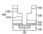
- FIGS. 1 to 4are schematic sectional views illustrating a method for forming a dual damascene pattern according to an embodiment of the present invention.
- FIGS. 1 to 4are schematic sectional views illustrating a method for forming a dual damascene pattern according to an embodiment of the present invention.
- a lower insulating layer 100is formed on a semiconductor substrate (not shown), and a patterned lower copper structure 150 is formed on the lower insulating layer 100 using a damascene process.
- a damascene processFor example, after a first trench is formed on the lower insulating layer 100 , a copper layer with which the first trench is filled is formed using an electroplating process, and thereafter, the lower copper structure 150 with which the first trench is filled is formed by polishing the copper layer using a chemical mechanical polishing (CMP) process.
- CMPchemical mechanical polishing
- the lower copper structure or layer 150may further contain a conventional adhesive layer (e.g., Ti) and/or diffusion barrier layer (e.g., TiN, TaN, etc.) and conventional vias for interconnecting with underlying layers of metallization and/or silicon (which may take the form of a polysilicon and/or metal silicide gate, a heavily doped source/drain junction in a silicon substrate, etc.).
- a conventional adhesive layere.g., Ti
- diffusion barrier layere.g., TiN, TaN, etc.
- conventional vias for interconnecting with underlying layers of metallization and/or siliconwhich may take the form of a polysilicon and/or metal silicide gate, a heavily doped source/drain junction in a silicon substrate, etc.
- a first protective film 210 for protecting the lower copper pattern 150 in a subsequent processis formed on the lower insulating layer 100 .
- the first protective film 210preferably comprises a silicon nitride layer. Also, the first protective film 210 can be used as an etch stop film in a subsequent via formation process.
- An insulating layer(which may comprise a plurality of insulating films) is formed on the first protective film 210 .
- the insulating layermay comprise a triple-layered structure having a first insulating film 310 , a second insulating film 330 and a third insulating film 350 .
- the first and third insulating films 310 and 350may comprise a silicon oxide layer made of plasma silane (P—SiH 4 ; e.g., an undoped silica glass [USG] from a feed gas comprising a silane [e.g., SiH 4 , Si 2 H 6 , etc.] and an oxygen source such as O 2 , O 3 , N 2 O, etc., decomposed in a plasma) using a chemical vapor deposition (CVD) process.
- the second insulating film 330may comprise a silicon oxide layer made of fluorine doped silica glass (FSG) having a dielectric constant relatively smaller than plasma silane.
- FSGfluorine doped silica glass
- the thickness of the first insulating film 310is similar to that of the third insulating film 350 , and the thickness of the second insulating film 330 is greater than those of the first and third insulating films 310 and 350 .
- the insulating layermay comprise a single layer or bilayer of doped or undoped silicate glass (e.g., USG, BSG, PSG, BPSG, or FSG containing a low concentration of fluorine).
- a second protective film 250is formed on the third insulating film 350 .
- the second protective film 250may comprise an insulating material, for example, a silicon nitride, having an etch rate similar to that of the first protective film 210 .
- the second protective film 250prevents a surface of the third insulating film 350 from being damaged or etched in a subsequent process.
- a first photoresist pattern 400is formed as a via etch mask for forming a via hole on the second protective film 250 .
- a via hole 410is formed using the first photoresist pattern 400 as an etch mask.
- the via hole 410is formed through the second protective film 250 and the third insulating film 350 , up to a certain depth into the second insulating film 330 .
- the viais etched to a target depth of about the total thickness of the insulator layer (e.g., insulator films 310 – 350 ) and the second protective layer 250 , minus the target depth of the trench divided by a target overetch value.
- the target overetch valuerelates to an overetch intended to allow for process variations due to error margins, and is determined empirically by known methods.
- the viamay be overetched by about 10%, making the target overetch value about 1.1.
- a second photoresist pattern(not shown) to be used as an etch mask for formation of a trench 430 is formed, and the insulating layer is anisotropically etched and/or patterned using the second photoresist pattern as the etch mask.
- the second protective film 250 , the third insulating film 350 , the second insulating film 330 and the first insulating film 310are etched in the trench-forming etch step.
- the trench 430is substantially formed after this etching process is completed.
- the etching process for forming the trench 430is performed to a target depth of the trench 430 . While the etching process is performed, the via hole 410 exposes the first protective film 210 on the lower copper pattern 150 . At this time, since the first protective film 210 comprises a material (e.g., silicon nitride) having an etch selectivity higher than that of silicon oxides (e.g., USG, FSG), the etching process for the via hole 410 is performed up to a point at which the first protective film 210 is exposed. Thereafter, the second photoresist pattern is removed.
- a materiale.g., silicon nitride
- silicon oxidese.g., USG, FSG
- the first protective layer 210 within the via hole 410is etched to expose the top surface of the lower copper pattern 150 .
- This etching processis performed as an entire surface etching process (i.e., without an etch mask).
- the second protective film 250is also etched away.
- dual damascene pattern 450composed of the via hole 410 and the trench 430 is completed.
- a copper interconnectionis implemented by forming an upper copper pattern (which may further contain a conventional adhesive and/or diffusion barrier layer as described above between the copper and the insulating layer or films) as an upper conductive layer with which the dual damascene pattern 450 is filled.
- a dual damascene pattern including a via hole and a trenchcan be simply implemented. Accordingly, the yield of semiconductor device can be improved, and product costs thereof can be reduced. In addition, since contamination and/or corrosion of the lower copper interconnection can be prevented, device reliability can be improved.
Landscapes
- Engineering & Computer Science (AREA)
- Physics & Mathematics (AREA)
- Condensed Matter Physics & Semiconductors (AREA)
- General Physics & Mathematics (AREA)
- Manufacturing & Machinery (AREA)
- Computer Hardware Design (AREA)
- Microelectronics & Electronic Packaging (AREA)
- Power Engineering (AREA)
- Internal Circuitry In Semiconductor Integrated Circuit Devices (AREA)
Abstract
Description
Claims (19)
Applications Claiming Priority (2)
| Application Number | Priority Date | Filing Date | Title |
|---|---|---|---|
| KR10-2003-0101799 | 2003-12-31 | ||
| KR10-2003-0101799AKR100529676B1 (en) | 2003-12-31 | 2003-12-31 | Method for fabricating dual damascene pattern |
Publications (2)
| Publication Number | Publication Date |
|---|---|
| US20050153542A1 US20050153542A1 (en) | 2005-07-14 |
| US7179734B2true US7179734B2 (en) | 2007-02-20 |
Family
ID=34737961
Family Applications (1)
| Application Number | Title | Priority Date | Filing Date |
|---|---|---|---|
| US11/026,881Expired - Fee RelatedUS7179734B2 (en) | 2003-12-31 | 2004-12-30 | Method for forming dual damascene pattern |
Country Status (4)
| Country | Link |
|---|---|
| US (1) | US7179734B2 (en) |
| JP (1) | JP2005197692A (en) |
| KR (1) | KR100529676B1 (en) |
| DE (1) | DE102004062835B4 (en) |
Cited By (3)
| Publication number | Priority date | Publication date | Assignee | Title |
|---|---|---|---|---|
| US20090261475A1 (en)* | 2005-12-26 | 2009-10-22 | Dong-Yeal Keum | Method for fabricating a metal interconnection using a dual damascene process and resulting semiconductor device |
| US20100164121A1 (en)* | 2008-12-31 | 2010-07-01 | Frank Feustel | Metallization system of a semiconductor device comprising extra-tapered transition vias |
| US20130183825A1 (en)* | 2012-01-18 | 2013-07-18 | En-Chiuan Liou | Method for manufacturing damascene structure |
Families Citing this family (8)
| Publication number | Priority date | Publication date | Assignee | Title |
|---|---|---|---|---|
| US7279210B2 (en)* | 2005-09-07 | 2007-10-09 | 3M Innovative Properties Company | Curable compositions, methods of making and using the same, and articles therefrom |
| KR100691105B1 (en)* | 2005-09-28 | 2007-03-09 | 동부일렉트로닉스 주식회사 | Copper wiring formation method using dual damascene process |
| US20070082469A1 (en)* | 2005-10-12 | 2007-04-12 | Peters John M | Forming heaters for phase change memories |
| KR100650766B1 (en)* | 2005-11-08 | 2006-11-27 | 주식회사 하이닉스반도체 | Manufacturing method of semiconductor device |
| KR100728486B1 (en)* | 2005-11-15 | 2007-06-13 | 동부일렉트로닉스 주식회사 | Wiring Formation Method of Semiconductor Device |
| US20070134917A1 (en)* | 2005-12-13 | 2007-06-14 | Taiwan Semiconductor Manufacturing Co., Ltd. | Partial-via-first dual-damascene process with tri-layer resist approach |
| KR100859476B1 (en)* | 2006-12-29 | 2008-09-24 | 동부일렉트로닉스 주식회사 | Semiconductor Device Formation Method |
| KR102500249B1 (en) | 2022-08-10 | 2023-02-16 | 유종형 | Moving military camp using truck camper |
Citations (8)
| Publication number | Priority date | Publication date | Assignee | Title |
|---|---|---|---|---|
| US4789648A (en) | 1985-10-28 | 1988-12-06 | International Business Machines Corporation | Method for producing coplanar multi-level metal/insulator films on a substrate and for forming patterned conductive lines simultaneously with stud vias |
| US5563105A (en) | 1994-09-30 | 1996-10-08 | International Business Machines Corporation | PECVD method of depositing fluorine doped oxide using a fluorine precursor containing a glass-forming element |
| US6066577A (en) | 1996-11-08 | 2000-05-23 | International Business Machines Corporation | Method for providing fluorine barrier layer between conductor and insulator for degradation prevention |
| US6153511A (en)* | 1998-10-14 | 2000-11-28 | Fujitsu Limited | Semiconductor device having a multilayered interconnection structure |
| US20020034874A1 (en)* | 1998-10-05 | 2002-03-21 | Hidemitsu Aoki | Method of manufacturing a semiconductor device |
| US6383907B1 (en)* | 1999-09-08 | 2002-05-07 | Sony Corporation | Process for fabricating a semiconductor device |
| EP1302981A2 (en) | 2001-10-10 | 2003-04-16 | Fujitsu Limited | Method of manufacturing semiconductor device having silicon carbide film |
| US6627540B2 (en)* | 2001-12-07 | 2003-09-30 | Samsung Electronics Co., Ltd. | Method for forming dual damascene structure in semiconductor device |
- 2003
- 2003-12-31KRKR10-2003-0101799Apatent/KR100529676B1/ennot_activeExpired - Fee Related
- 2004
- 2004-12-24JPJP2004373214Apatent/JP2005197692A/enactivePending
- 2004-12-27DEDE102004062835Apatent/DE102004062835B4/ennot_activeExpired - Fee Related
- 2004-12-30USUS11/026,881patent/US7179734B2/ennot_activeExpired - Fee Related
Patent Citations (10)
| Publication number | Priority date | Publication date | Assignee | Title |
|---|---|---|---|---|
| US4789648A (en) | 1985-10-28 | 1988-12-06 | International Business Machines Corporation | Method for producing coplanar multi-level metal/insulator films on a substrate and for forming patterned conductive lines simultaneously with stud vias |
| US5563105A (en) | 1994-09-30 | 1996-10-08 | International Business Machines Corporation | PECVD method of depositing fluorine doped oxide using a fluorine precursor containing a glass-forming element |
| US6066577A (en) | 1996-11-08 | 2000-05-23 | International Business Machines Corporation | Method for providing fluorine barrier layer between conductor and insulator for degradation prevention |
| US6310300B1 (en) | 1996-11-08 | 2001-10-30 | International Business Machines Corporation | Fluorine-free barrier layer between conductor and insulator for degradation prevention |
| US20020034874A1 (en)* | 1998-10-05 | 2002-03-21 | Hidemitsu Aoki | Method of manufacturing a semiconductor device |
| US6387821B1 (en)* | 1998-10-05 | 2002-05-14 | Nec Corporation | Method of manufacturing a semiconductor device |
| US6153511A (en)* | 1998-10-14 | 2000-11-28 | Fujitsu Limited | Semiconductor device having a multilayered interconnection structure |
| US6383907B1 (en)* | 1999-09-08 | 2002-05-07 | Sony Corporation | Process for fabricating a semiconductor device |
| EP1302981A2 (en) | 2001-10-10 | 2003-04-16 | Fujitsu Limited | Method of manufacturing semiconductor device having silicon carbide film |
| US6627540B2 (en)* | 2001-12-07 | 2003-09-30 | Samsung Electronics Co., Ltd. | Method for forming dual damascene structure in semiconductor device |
Cited By (6)
| Publication number | Priority date | Publication date | Assignee | Title |
|---|---|---|---|---|
| US20090261475A1 (en)* | 2005-12-26 | 2009-10-22 | Dong-Yeal Keum | Method for fabricating a metal interconnection using a dual damascene process and resulting semiconductor device |
| US8013423B2 (en)* | 2005-12-26 | 2011-09-06 | Dongbu Hitek Co., Ltd. | Method for fabricating a metal interconnection using a dual damascene process and resulting semiconductor device |
| US20100164121A1 (en)* | 2008-12-31 | 2010-07-01 | Frank Feustel | Metallization system of a semiconductor device comprising extra-tapered transition vias |
| US8835303B2 (en)* | 2008-12-31 | 2014-09-16 | Advanced Micro Devices, Inc. | Metallization system of a semiconductor device comprising extra-tapered transition vias |
| US20130183825A1 (en)* | 2012-01-18 | 2013-07-18 | En-Chiuan Liou | Method for manufacturing damascene structure |
| US8883638B2 (en)* | 2012-01-18 | 2014-11-11 | United Microelectronics Corp. | Method for manufacturing damascene structure involving dummy via holes |
Also Published As
| Publication number | Publication date |
|---|---|
| KR20050069586A (en) | 2005-07-05 |
| KR100529676B1 (en) | 2005-11-17 |
| DE102004062835B4 (en) | 2006-12-21 |
| JP2005197692A (en) | 2005-07-21 |
| DE102004062835A1 (en) | 2005-08-04 |
| US20050153542A1 (en) | 2005-07-14 |
Similar Documents
| Publication | Publication Date | Title |
|---|---|---|
| US6051508A (en) | Manufacturing method of semiconductor device | |
| US6399512B1 (en) | Method of making metallization and contact structures in an integrated circuit comprising an etch stop layer | |
| JP4347637B2 (en) | Method of forming metal wiring for semiconductor device using buffer layer on trench side wall and device manufactured thereby | |
| US6846741B2 (en) | Sacrificial metal spacer damascene process | |
| US7595554B2 (en) | Interconnect structure with dielectric air gaps | |
| KR100421154B1 (en) | Method of making metallization and contact structures in an integrated circuit | |
| US7436009B2 (en) | Via structures and trench structures and dual damascene structures | |
| US7381637B2 (en) | Metal spacer in single and dual damascence processing | |
| US20070252277A1 (en) | Semiconductor devices and fabrication method thereof | |
| US20070232048A1 (en) | Damascene interconnection having a SiCOH low k layer | |
| US7179734B2 (en) | Method for forming dual damascene pattern | |
| JP5178025B2 (en) | Manufacturing method of semiconductor memory device | |
| US5625231A (en) | Low cost solution to high aspect ratio contact/via adhesion layer application for deep sub-half micrometer back-end-of line technology | |
| US7397124B2 (en) | Process of metal interconnects | |
| US20050263892A1 (en) | Method of forming copper interconnection in semiconductor device and semiconductor device using the same | |
| US7557038B2 (en) | Method for fabricating self-aligned contact hole | |
| US20020072217A1 (en) | Method for improving contact reliability in semiconductor devices | |
| US7112537B2 (en) | Method of fabricating interconnection structure of semiconductor device | |
| US7704820B2 (en) | Fabricating method of metal line | |
| KR100602132B1 (en) | How to form a dual damascene pattern | |
| KR20030002119A (en) | Method for forming via hole by dual damascene process | |
| US7901976B1 (en) | Method of forming borderless contacts | |
| KR100268515B1 (en) | A manufacturing method of contact holes | |
| KR100784105B1 (en) | Manufacturing Method of Semiconductor Device | |
| KR100571408B1 (en) | Dual damascene wiring manufacturing method of semiconductor device |
Legal Events
| Date | Code | Title | Description |
|---|---|---|---|
| AS | Assignment | Owner name:DONGBUANAM SEMICONDUCTOR INC., KOREA, REPUBLIC OF Free format text:ASSIGNMENT OF ASSIGNORS INTEREST;ASSIGNOR:KEUM, DONG-YEAL;REEL/FRAME:016146/0137 Effective date:20041228 | |
| AS | Assignment | Owner name:DONGBU ELECTRONICS CO., LTD.,KOREA, REPUBLIC OF Free format text:CHANGE OF NAME;ASSIGNOR:DONGANAM SEMICONDUCTOR INC.;REEL/FRAME:017749/0335 Effective date:20060328 Owner name:DONGBU ELECTRONICS CO., LTD., KOREA, REPUBLIC OF Free format text:CHANGE OF NAME;ASSIGNOR:DONGANAM SEMICONDUCTOR INC.;REEL/FRAME:017749/0335 Effective date:20060328 | |
| AS | Assignment | Owner name:DONGBU ELECTRONICS CO., LTD., KOREA, REPUBLIC OF Free format text:CORRECTIVE ASSIGNMENT TO CORRECT THE ASSIGNOR PREVIOUSLY RECORDED ON REEL 017749 FRAME 0335;ASSIGNOR:DONGBUANAM SEMICONDUCTOR INC.;REEL/FRAME:017821/0670 Effective date:20060328 Owner name:DONGBU ELECTRONICS CO., LTD.,KOREA, REPUBLIC OF Free format text:CORRECTIVE ASSIGNMENT TO CORRECT THE ASSIGNOR PREVIOUSLY RECORDED ON REEL 017749 FRAME 0335. ASSIGNOR(S) HEREBY CONFIRMS THE ASSIGNOR SHOULD BE "DONGBUANAM SEMICONDUCTOR INC.";ASSIGNOR:DONGBUANAM SEMICONDUCTOR INC.;REEL/FRAME:017821/0670 Effective date:20060328 Owner name:DONGBU ELECTRONICS CO., LTD., KOREA, REPUBLIC OF Free format text:CORRECTIVE ASSIGNMENT TO CORRECT THE ASSIGNOR PREVIOUSLY RECORDED ON REEL 017749 FRAME 0335. ASSIGNOR(S) HEREBY CONFIRMS THE ASSIGNOR SHOULD BE "DONGBUANAM SEMICONDUCTOR INC.";ASSIGNOR:DONGBUANAM SEMICONDUCTOR INC.;REEL/FRAME:017821/0670 Effective date:20060328 | |
| FEPP | Fee payment procedure | Free format text:PAYOR NUMBER ASSIGNED (ORIGINAL EVENT CODE: ASPN); ENTITY STATUS OF PATENT OWNER: LARGE ENTITY | |
| FPAY | Fee payment | Year of fee payment:4 | |
| REMI | Maintenance fee reminder mailed | ||
| LAPS | Lapse for failure to pay maintenance fees | ||
| STCH | Information on status: patent discontinuation | Free format text:PATENT EXPIRED DUE TO NONPAYMENT OF MAINTENANCE FEES UNDER 37 CFR 1.362 | |
| FP | Lapsed due to failure to pay maintenance fee | Effective date:20150220 |