US7179670B2 - Flip-chip light emitting diode device without sub-mount - Google Patents
Flip-chip light emitting diode device without sub-mountDownload PDFInfo
- Publication number
- US7179670B2 US7179670B2US10/794,935US79493504AUS7179670B2US 7179670 B2US7179670 B2US 7179670B2US 79493504 AUS79493504 AUS 79493504AUS 7179670 B2US7179670 B2US 7179670B2
- Authority
- US
- United States
- Prior art keywords
- type
- light emitting
- dielectric layer
- disposing
- contact pads
- Prior art date
- Legal status (The legal status is an assumption and is not a legal conclusion. Google has not performed a legal analysis and makes no representation as to the accuracy of the status listed.)
- Expired - Lifetime, expires
Links
- 238000000926separation methodMethods0.000claimsabstractdescription59
- 238000004891communicationMethods0.000claimsabstractdescription5
- 238000000034methodMethods0.000claimsdescription91
- 239000000758substrateSubstances0.000claimsdescription52
- 238000012545processingMethods0.000claimsdescription40
- 230000008569processEffects0.000claimsdescription38
- 239000004020conductorSubstances0.000claimsdescription35
- 239000000463materialSubstances0.000claimsdescription24
- 238000000151depositionMethods0.000claimsdescription16
- 239000008393encapsulating agentSubstances0.000claimsdescription13
- 229910052751metalInorganic materials0.000claimsdescription13
- 239000002184metalSubstances0.000claimsdescription13
- 239000011248coating agentSubstances0.000claimsdescription10
- 238000000576coating methodMethods0.000claimsdescription10
- OAICVXFJPJFONN-UHFFFAOYSA-NPhosphorusChemical compound[P]OAICVXFJPJFONN-UHFFFAOYSA-N0.000claimsdescription8
- 238000009713electroplatingMethods0.000claimsdescription8
- 230000004888barrier functionEffects0.000claimsdescription7
- PCHJSUWPFVWCPO-UHFFFAOYSA-NgoldChemical compound[Au]PCHJSUWPFVWCPO-UHFFFAOYSA-N0.000claimsdescription7
- 229910052737goldInorganic materials0.000claimsdescription7
- 239000010931goldSubstances0.000claimsdescription7
- 238000010438heat treatmentMethods0.000claimsdescription6
- 230000003287optical effectEffects0.000claimsdescription6
- 238000007789sealingMethods0.000claimsdescription6
- 239000004952PolyamideSubstances0.000claimsdescription3
- ATJFFYVFTNAWJD-UHFFFAOYSA-NTinChemical compound[Sn]ATJFFYVFTNAWJD-UHFFFAOYSA-N0.000claimsdescription3
- 239000000956alloySubstances0.000claimsdescription3
- 229910045601alloyInorganic materials0.000claimsdescription3
- 230000000694effectsEffects0.000claimsdescription3
- 229920002647polyamidePolymers0.000claimsdescription3
- 238000005476solderingMethods0.000claimsdescription3
- 235000001674Agaricus brunnescensNutrition0.000claimsdescription2
- 238000004026adhesive bondingMethods0.000claimsdescription2
- 230000004907fluxEffects0.000claimsdescription2
- 230000008018meltingEffects0.000claimsdescription2
- 238000002844meltingMethods0.000claimsdescription2
- 239000012778molding materialSubstances0.000claims1
- 230000015572biosynthetic processEffects0.000description19
- 229910002601GaNInorganic materials0.000description8
- PXHVJJICTQNCMI-UHFFFAOYSA-NNickelChemical compound[Ni]PXHVJJICTQNCMI-UHFFFAOYSA-N0.000description8
- 238000003892spreadingMethods0.000description7
- 230000007480spreadingEffects0.000description7
- 230000008021depositionEffects0.000description6
- 238000009792diffusion processMethods0.000description6
- 238000004519manufacturing processMethods0.000description6
- JMASRVWKEDWRBT-UHFFFAOYSA-NGallium nitrideChemical compound[Ga]#NJMASRVWKEDWRBT-UHFFFAOYSA-N0.000description5
- 238000000605extractionMethods0.000description5
- 229920002120photoresistant polymerPolymers0.000description5
- VYPSYNLAJGMNEJ-UHFFFAOYSA-NSilicium dioxideChemical compoundO=[Si]=OVYPSYNLAJGMNEJ-UHFFFAOYSA-N0.000description4
- 238000005275alloyingMethods0.000description4
- 230000008901benefitEffects0.000description4
- 238000005253claddingMethods0.000description4
- 238000002955isolationMethods0.000description4
- 229910052759nickelInorganic materials0.000description4
- BQCADISMDOOEFD-UHFFFAOYSA-NSilverChemical compound[Ag]BQCADISMDOOEFD-UHFFFAOYSA-N0.000description3
- RTAQQCXQSZGOHL-UHFFFAOYSA-NTitaniumChemical compound[Ti]RTAQQCXQSZGOHL-UHFFFAOYSA-N0.000description3
- RNQKDQAVIXDKAG-UHFFFAOYSA-Naluminum galliumChemical compound[Al].[Ga]RNQKDQAVIXDKAG-UHFFFAOYSA-N0.000description3
- 238000001465metallisationMethods0.000description3
- 229910052709silverInorganic materials0.000description3
- 239000004332silverSubstances0.000description3
- 239000010936titaniumSubstances0.000description3
- 229910052719titaniumInorganic materials0.000description3
- 238000007738vacuum evaporationMethods0.000description3
- 229910052581Si3N4Inorganic materials0.000description2
- 230000004075alterationEffects0.000description2
- 238000011109contaminationMethods0.000description2
- 239000003989dielectric materialSubstances0.000description2
- 238000005401electroluminescenceMethods0.000description2
- 229910052738indiumInorganic materials0.000description2
- APFVFJFRJDLVQX-UHFFFAOYSA-Nindium atomChemical compound[In]APFVFJFRJDLVQX-UHFFFAOYSA-N0.000description2
- 238000001459lithographyMethods0.000description2
- 238000012986modificationMethods0.000description2
- 230000004048modificationEffects0.000description2
- 238000004806packaging method and processMethods0.000description2
- 238000011112process operationMethods0.000description2
- 229910052594sapphireInorganic materials0.000description2
- 239000010980sapphireSubstances0.000description2
- HBMJWWWQQXIZIP-UHFFFAOYSA-Nsilicon carbideChemical compound[Si+]#[C-]HBMJWWWQQXIZIP-UHFFFAOYSA-N0.000description2
- 229910010271silicon carbideInorganic materials0.000description2
- 235000012239silicon dioxideNutrition0.000description2
- 239000000377silicon dioxideSubstances0.000description2
- HQVNEWCFYHHQES-UHFFFAOYSA-Nsilicon nitrideChemical compoundN12[Si]34N5[Si]62N3[Si]51N64HQVNEWCFYHHQES-UHFFFAOYSA-N0.000description2
- 229910000679solderInorganic materials0.000description2
- 238000004544sputter depositionMethods0.000description2
- 239000000126substanceSubstances0.000description2
- RYGMFSIKBFXOCR-UHFFFAOYSA-NCopperChemical compound[Cu]RYGMFSIKBFXOCR-UHFFFAOYSA-N0.000description1
- 239000004593EpoxySubstances0.000description1
- GYHNNYVSQQEPJS-UHFFFAOYSA-NGalliumChemical compound[Ga]GYHNNYVSQQEPJS-UHFFFAOYSA-N0.000description1
- 230000006978adaptationEffects0.000description1
- 229910052782aluminiumInorganic materials0.000description1
- XAGFODPZIPBFFR-UHFFFAOYSA-NaluminiumChemical compound[Al]XAGFODPZIPBFFR-UHFFFAOYSA-N0.000description1
- 238000006243chemical reactionMethods0.000description1
- 239000002131composite materialSubstances0.000description1
- 230000001010compromised effectEffects0.000description1
- 229910052802copperInorganic materials0.000description1
- 239000010949copperSubstances0.000description1
- PMHQVHHXPFUNSP-UHFFFAOYSA-Mcopper(1+);methylsulfanylmethane;bromideChemical compoundBr[Cu].CSCPMHQVHHXPFUNSP-UHFFFAOYSA-M0.000description1
- 230000008878couplingEffects0.000description1
- 238000010168coupling processMethods0.000description1
- 238000005859coupling reactionMethods0.000description1
- 238000005520cutting processMethods0.000description1
- 230000007812deficiencyEffects0.000description1
- 229910003460diamondInorganic materials0.000description1
- 239000010432diamondSubstances0.000description1
- 238000009429electrical wiringMethods0.000description1
- 239000007772electrode materialSubstances0.000description1
- 238000000407epitaxyMethods0.000description1
- 229910052733galliumInorganic materials0.000description1
- 239000011521glassSubstances0.000description1
- 229930195733hydrocarbonNatural products0.000description1
- 150000002430hydrocarbonsChemical class0.000description1
- 238000005286illuminationMethods0.000description1
- 238000003698laser cuttingMethods0.000description1
- 239000000203mixtureSubstances0.000description1
- 230000001681protective effectEffects0.000description1
- 230000009467reductionEffects0.000description1
- 238000012546transferMethods0.000description1
- 239000012808vapor phaseSubstances0.000description1
Images


Classifications
- H—ELECTRICITY
- H10—SEMICONDUCTOR DEVICES; ELECTRIC SOLID-STATE DEVICES NOT OTHERWISE PROVIDED FOR
- H10H—INORGANIC LIGHT-EMITTING SEMICONDUCTOR DEVICES HAVING POTENTIAL BARRIERS
- H10H20/00—Individual inorganic light-emitting semiconductor devices having potential barriers, e.g. light-emitting diodes [LED]
- H10H20/80—Constructional details
- H10H20/85—Packages
- H10H20/857—Interconnections, e.g. lead-frames, bond wires or solder balls
- H—ELECTRICITY
- H01—ELECTRIC ELEMENTS
- H01L—SEMICONDUCTOR DEVICES NOT COVERED BY CLASS H10
- H01L2224/00—Indexing scheme for arrangements for connecting or disconnecting semiconductor or solid-state bodies and methods related thereto as covered by H01L24/00
- H01L2224/01—Means for bonding being attached to, or being formed on, the surface to be connected, e.g. chip-to-package, die-attach, "first-level" interconnects; Manufacturing methods related thereto
- H01L2224/02—Bonding areas; Manufacturing methods related thereto
- H01L2224/03—Manufacturing methods
- H01L2224/034—Manufacturing methods by blanket deposition of the material of the bonding area
- H01L2224/03444—Manufacturing methods by blanket deposition of the material of the bonding area in gaseous form
- H01L2224/0345—Physical vapour deposition [PVD], e.g. evaporation, or sputtering
- H—ELECTRICITY
- H01—ELECTRIC ELEMENTS
- H01L—SEMICONDUCTOR DEVICES NOT COVERED BY CLASS H10
- H01L2224/00—Indexing scheme for arrangements for connecting or disconnecting semiconductor or solid-state bodies and methods related thereto as covered by H01L24/00
- H01L2224/01—Means for bonding being attached to, or being formed on, the surface to be connected, e.g. chip-to-package, die-attach, "first-level" interconnects; Manufacturing methods related thereto
- H01L2224/02—Bonding areas; Manufacturing methods related thereto
- H01L2224/03—Manufacturing methods
- H01L2224/034—Manufacturing methods by blanket deposition of the material of the bonding area
- H01L2224/0346—Plating
- H01L2224/03462—Electroplating
- H—ELECTRICITY
- H01—ELECTRIC ELEMENTS
- H01L—SEMICONDUCTOR DEVICES NOT COVERED BY CLASS H10
- H01L2224/00—Indexing scheme for arrangements for connecting or disconnecting semiconductor or solid-state bodies and methods related thereto as covered by H01L24/00
- H01L2224/01—Means for bonding being attached to, or being formed on, the surface to be connected, e.g. chip-to-package, die-attach, "first-level" interconnects; Manufacturing methods related thereto
- H01L2224/02—Bonding areas; Manufacturing methods related thereto
- H01L2224/04—Structure, shape, material or disposition of the bonding areas prior to the connecting process
- H01L2224/0401—Bonding areas specifically adapted for bump connectors, e.g. under bump metallisation [UBM]
- H—ELECTRICITY
- H01—ELECTRIC ELEMENTS
- H01L—SEMICONDUCTOR DEVICES NOT COVERED BY CLASS H10
- H01L2224/00—Indexing scheme for arrangements for connecting or disconnecting semiconductor or solid-state bodies and methods related thereto as covered by H01L24/00
- H01L2224/01—Means for bonding being attached to, or being formed on, the surface to be connected, e.g. chip-to-package, die-attach, "first-level" interconnects; Manufacturing methods related thereto
- H01L2224/02—Bonding areas; Manufacturing methods related thereto
- H01L2224/04—Structure, shape, material or disposition of the bonding areas prior to the connecting process
- H01L2224/04026—Bonding areas specifically adapted for layer connectors
- H—ELECTRICITY
- H01—ELECTRIC ELEMENTS
- H01L—SEMICONDUCTOR DEVICES NOT COVERED BY CLASS H10
- H01L2224/00—Indexing scheme for arrangements for connecting or disconnecting semiconductor or solid-state bodies and methods related thereto as covered by H01L24/00
- H01L2224/01—Means for bonding being attached to, or being formed on, the surface to be connected, e.g. chip-to-package, die-attach, "first-level" interconnects; Manufacturing methods related thereto
- H01L2224/02—Bonding areas; Manufacturing methods related thereto
- H01L2224/04—Structure, shape, material or disposition of the bonding areas prior to the connecting process
- H01L2224/05—Structure, shape, material or disposition of the bonding areas prior to the connecting process of an individual bonding area
- H01L2224/05001—Internal layers
- H01L2224/05005—Structure
- H—ELECTRICITY
- H01—ELECTRIC ELEMENTS
- H01L—SEMICONDUCTOR DEVICES NOT COVERED BY CLASS H10
- H01L2224/00—Indexing scheme for arrangements for connecting or disconnecting semiconductor or solid-state bodies and methods related thereto as covered by H01L24/00
- H01L2224/01—Means for bonding being attached to, or being formed on, the surface to be connected, e.g. chip-to-package, die-attach, "first-level" interconnects; Manufacturing methods related thereto
- H01L2224/02—Bonding areas; Manufacturing methods related thereto
- H01L2224/04—Structure, shape, material or disposition of the bonding areas prior to the connecting process
- H01L2224/05—Structure, shape, material or disposition of the bonding areas prior to the connecting process of an individual bonding area
- H01L2224/05001—Internal layers
- H01L2224/0502—Disposition
- H01L2224/05023—Disposition the whole internal layer protruding from the surface
- H—ELECTRICITY
- H01—ELECTRIC ELEMENTS
- H01L—SEMICONDUCTOR DEVICES NOT COVERED BY CLASS H10
- H01L2224/00—Indexing scheme for arrangements for connecting or disconnecting semiconductor or solid-state bodies and methods related thereto as covered by H01L24/00
- H01L2224/01—Means for bonding being attached to, or being formed on, the surface to be connected, e.g. chip-to-package, die-attach, "first-level" interconnects; Manufacturing methods related thereto
- H01L2224/02—Bonding areas; Manufacturing methods related thereto
- H01L2224/04—Structure, shape, material or disposition of the bonding areas prior to the connecting process
- H01L2224/05—Structure, shape, material or disposition of the bonding areas prior to the connecting process of an individual bonding area
- H01L2224/05001—Internal layers
- H01L2224/0502—Disposition
- H01L2224/05026—Disposition the internal layer being disposed in a recess of the surface
- H01L2224/05027—Disposition the internal layer being disposed in a recess of the surface the internal layer extending out of an opening
- H—ELECTRICITY
- H01—ELECTRIC ELEMENTS
- H01L—SEMICONDUCTOR DEVICES NOT COVERED BY CLASS H10
- H01L2224/00—Indexing scheme for arrangements for connecting or disconnecting semiconductor or solid-state bodies and methods related thereto as covered by H01L24/00
- H01L2224/01—Means for bonding being attached to, or being formed on, the surface to be connected, e.g. chip-to-package, die-attach, "first-level" interconnects; Manufacturing methods related thereto
- H01L2224/02—Bonding areas; Manufacturing methods related thereto
- H01L2224/04—Structure, shape, material or disposition of the bonding areas prior to the connecting process
- H01L2224/05—Structure, shape, material or disposition of the bonding areas prior to the connecting process of an individual bonding area
- H01L2224/05001—Internal layers
- H01L2224/05075—Plural internal layers
- H01L2224/0508—Plural internal layers being stacked
- H—ELECTRICITY
- H01—ELECTRIC ELEMENTS
- H01L—SEMICONDUCTOR DEVICES NOT COVERED BY CLASS H10
- H01L2224/00—Indexing scheme for arrangements for connecting or disconnecting semiconductor or solid-state bodies and methods related thereto as covered by H01L24/00
- H01L2224/01—Means for bonding being attached to, or being formed on, the surface to be connected, e.g. chip-to-package, die-attach, "first-level" interconnects; Manufacturing methods related thereto
- H01L2224/02—Bonding areas; Manufacturing methods related thereto
- H01L2224/04—Structure, shape, material or disposition of the bonding areas prior to the connecting process
- H01L2224/05—Structure, shape, material or disposition of the bonding areas prior to the connecting process of an individual bonding area
- H01L2224/05001—Internal layers
- H01L2224/05099—Material
- H01L2224/051—Material with a principal constituent of the material being a metal or a metalloid, e.g. boron [B], silicon [Si], germanium [Ge], arsenic [As], antimony [Sb], tellurium [Te] and polonium [Po], and alloys thereof
- H01L2224/05138—Material with a principal constituent of the material being a metal or a metalloid, e.g. boron [B], silicon [Si], germanium [Ge], arsenic [As], antimony [Sb], tellurium [Te] and polonium [Po], and alloys thereof the principal constituent melting at a temperature of greater than or equal to 950°C and less than 1550°C
- H01L2224/05139—Silver [Ag] as principal constituent
- H—ELECTRICITY
- H01—ELECTRIC ELEMENTS
- H01L—SEMICONDUCTOR DEVICES NOT COVERED BY CLASS H10
- H01L2224/00—Indexing scheme for arrangements for connecting or disconnecting semiconductor or solid-state bodies and methods related thereto as covered by H01L24/00
- H01L2224/01—Means for bonding being attached to, or being formed on, the surface to be connected, e.g. chip-to-package, die-attach, "first-level" interconnects; Manufacturing methods related thereto
- H01L2224/02—Bonding areas; Manufacturing methods related thereto
- H01L2224/04—Structure, shape, material or disposition of the bonding areas prior to the connecting process
- H01L2224/05—Structure, shape, material or disposition of the bonding areas prior to the connecting process of an individual bonding area
- H01L2224/05001—Internal layers
- H01L2224/05099—Material
- H01L2224/051—Material with a principal constituent of the material being a metal or a metalloid, e.g. boron [B], silicon [Si], germanium [Ge], arsenic [As], antimony [Sb], tellurium [Te] and polonium [Po], and alloys thereof
- H01L2224/05138—Material with a principal constituent of the material being a metal or a metalloid, e.g. boron [B], silicon [Si], germanium [Ge], arsenic [As], antimony [Sb], tellurium [Te] and polonium [Po], and alloys thereof the principal constituent melting at a temperature of greater than or equal to 950°C and less than 1550°C
- H01L2224/05144—Gold [Au] as principal constituent
- H—ELECTRICITY
- H01—ELECTRIC ELEMENTS
- H01L—SEMICONDUCTOR DEVICES NOT COVERED BY CLASS H10
- H01L2224/00—Indexing scheme for arrangements for connecting or disconnecting semiconductor or solid-state bodies and methods related thereto as covered by H01L24/00
- H01L2224/01—Means for bonding being attached to, or being formed on, the surface to be connected, e.g. chip-to-package, die-attach, "first-level" interconnects; Manufacturing methods related thereto
- H01L2224/02—Bonding areas; Manufacturing methods related thereto
- H01L2224/04—Structure, shape, material or disposition of the bonding areas prior to the connecting process
- H01L2224/05—Structure, shape, material or disposition of the bonding areas prior to the connecting process of an individual bonding area
- H01L2224/05001—Internal layers
- H01L2224/05099—Material
- H01L2224/051—Material with a principal constituent of the material being a metal or a metalloid, e.g. boron [B], silicon [Si], germanium [Ge], arsenic [As], antimony [Sb], tellurium [Te] and polonium [Po], and alloys thereof
- H01L2224/05138—Material with a principal constituent of the material being a metal or a metalloid, e.g. boron [B], silicon [Si], germanium [Ge], arsenic [As], antimony [Sb], tellurium [Te] and polonium [Po], and alloys thereof the principal constituent melting at a temperature of greater than or equal to 950°C and less than 1550°C
- H01L2224/05155—Nickel [Ni] as principal constituent
- H—ELECTRICITY
- H01—ELECTRIC ELEMENTS
- H01L—SEMICONDUCTOR DEVICES NOT COVERED BY CLASS H10
- H01L2224/00—Indexing scheme for arrangements for connecting or disconnecting semiconductor or solid-state bodies and methods related thereto as covered by H01L24/00
- H01L2224/01—Means for bonding being attached to, or being formed on, the surface to be connected, e.g. chip-to-package, die-attach, "first-level" interconnects; Manufacturing methods related thereto
- H01L2224/02—Bonding areas; Manufacturing methods related thereto
- H01L2224/04—Structure, shape, material or disposition of the bonding areas prior to the connecting process
- H01L2224/05—Structure, shape, material or disposition of the bonding areas prior to the connecting process of an individual bonding area
- H01L2224/0554—External layer
- H01L2224/0556—Disposition
- H01L2224/05563—Only on parts of the surface of the internal layer
- H01L2224/05564—Only on the bonding interface of the bonding area
- H—ELECTRICITY
- H01—ELECTRIC ELEMENTS
- H01L—SEMICONDUCTOR DEVICES NOT COVERED BY CLASS H10
- H01L2224/00—Indexing scheme for arrangements for connecting or disconnecting semiconductor or solid-state bodies and methods related thereto as covered by H01L24/00
- H01L2224/01—Means for bonding being attached to, or being formed on, the surface to be connected, e.g. chip-to-package, die-attach, "first-level" interconnects; Manufacturing methods related thereto
- H01L2224/02—Bonding areas; Manufacturing methods related thereto
- H01L2224/04—Structure, shape, material or disposition of the bonding areas prior to the connecting process
- H01L2224/05—Structure, shape, material or disposition of the bonding areas prior to the connecting process of an individual bonding area
- H01L2224/0554—External layer
- H01L2224/0556—Disposition
- H01L2224/05568—Disposition the whole external layer protruding from the surface
- H—ELECTRICITY
- H01—ELECTRIC ELEMENTS
- H01L—SEMICONDUCTOR DEVICES NOT COVERED BY CLASS H10
- H01L2224/00—Indexing scheme for arrangements for connecting or disconnecting semiconductor or solid-state bodies and methods related thereto as covered by H01L24/00
- H01L2224/01—Means for bonding being attached to, or being formed on, the surface to be connected, e.g. chip-to-package, die-attach, "first-level" interconnects; Manufacturing methods related thereto
- H01L2224/02—Bonding areas; Manufacturing methods related thereto
- H01L2224/04—Structure, shape, material or disposition of the bonding areas prior to the connecting process
- H01L2224/05—Structure, shape, material or disposition of the bonding areas prior to the connecting process of an individual bonding area
- H01L2224/0554—External layer
- H01L2224/05599—Material
- H01L2224/056—Material with a principal constituent of the material being a metal or a metalloid, e.g. boron [B], silicon [Si], germanium [Ge], arsenic [As], antimony [Sb], tellurium [Te] and polonium [Po], and alloys thereof
- H01L2224/05601—Material with a principal constituent of the material being a metal or a metalloid, e.g. boron [B], silicon [Si], germanium [Ge], arsenic [As], antimony [Sb], tellurium [Te] and polonium [Po], and alloys thereof the principal constituent melting at a temperature of less than 400°C
- H01L2224/05611—Tin [Sn] as principal constituent
- H—ELECTRICITY
- H01—ELECTRIC ELEMENTS
- H01L—SEMICONDUCTOR DEVICES NOT COVERED BY CLASS H10
- H01L2224/00—Indexing scheme for arrangements for connecting or disconnecting semiconductor or solid-state bodies and methods related thereto as covered by H01L24/00
- H01L2224/01—Means for bonding being attached to, or being formed on, the surface to be connected, e.g. chip-to-package, die-attach, "first-level" interconnects; Manufacturing methods related thereto
- H01L2224/10—Bump connectors; Manufacturing methods related thereto
- H01L2224/12—Structure, shape, material or disposition of the bump connectors prior to the connecting process
- H01L2224/13—Structure, shape, material or disposition of the bump connectors prior to the connecting process of an individual bump connector
- H01L2224/13001—Core members of the bump connector
- H01L2224/13099—Material
- H01L2224/131—Material with a principal constituent of the material being a metal or a metalloid, e.g. boron [B], silicon [Si], germanium [Ge], arsenic [As], antimony [Sb], tellurium [Te] and polonium [Po], and alloys thereof
- H01L2224/13138—Material with a principal constituent of the material being a metal or a metalloid, e.g. boron [B], silicon [Si], germanium [Ge], arsenic [As], antimony [Sb], tellurium [Te] and polonium [Po], and alloys thereof the principal constituent melting at a temperature of greater than or equal to 950°C and less than 1550°C
- H01L2224/13139—Silver [Ag] as principal constituent
- H—ELECTRICITY
- H01—ELECTRIC ELEMENTS
- H01L—SEMICONDUCTOR DEVICES NOT COVERED BY CLASS H10
- H01L2224/00—Indexing scheme for arrangements for connecting or disconnecting semiconductor or solid-state bodies and methods related thereto as covered by H01L24/00
- H01L2224/01—Means for bonding being attached to, or being formed on, the surface to be connected, e.g. chip-to-package, die-attach, "first-level" interconnects; Manufacturing methods related thereto
- H01L2224/10—Bump connectors; Manufacturing methods related thereto
- H01L2224/12—Structure, shape, material or disposition of the bump connectors prior to the connecting process
- H01L2224/13—Structure, shape, material or disposition of the bump connectors prior to the connecting process of an individual bump connector
- H01L2224/13001—Core members of the bump connector
- H01L2224/13099—Material
- H01L2224/131—Material with a principal constituent of the material being a metal or a metalloid, e.g. boron [B], silicon [Si], germanium [Ge], arsenic [As], antimony [Sb], tellurium [Te] and polonium [Po], and alloys thereof
- H01L2224/13138—Material with a principal constituent of the material being a metal or a metalloid, e.g. boron [B], silicon [Si], germanium [Ge], arsenic [As], antimony [Sb], tellurium [Te] and polonium [Po], and alloys thereof the principal constituent melting at a temperature of greater than or equal to 950°C and less than 1550°C
- H01L2224/13144—Gold [Au] as principal constituent
- H—ELECTRICITY
- H01—ELECTRIC ELEMENTS
- H01L—SEMICONDUCTOR DEVICES NOT COVERED BY CLASS H10
- H01L2224/00—Indexing scheme for arrangements for connecting or disconnecting semiconductor or solid-state bodies and methods related thereto as covered by H01L24/00
- H01L2224/01—Means for bonding being attached to, or being formed on, the surface to be connected, e.g. chip-to-package, die-attach, "first-level" interconnects; Manufacturing methods related thereto
- H01L2224/10—Bump connectors; Manufacturing methods related thereto
- H01L2224/12—Structure, shape, material or disposition of the bump connectors prior to the connecting process
- H01L2224/13—Structure, shape, material or disposition of the bump connectors prior to the connecting process of an individual bump connector
- H01L2224/13001—Core members of the bump connector
- H01L2224/13099—Material
- H01L2224/131—Material with a principal constituent of the material being a metal or a metalloid, e.g. boron [B], silicon [Si], germanium [Ge], arsenic [As], antimony [Sb], tellurium [Te] and polonium [Po], and alloys thereof
- H01L2224/13138—Material with a principal constituent of the material being a metal or a metalloid, e.g. boron [B], silicon [Si], germanium [Ge], arsenic [As], antimony [Sb], tellurium [Te] and polonium [Po], and alloys thereof the principal constituent melting at a temperature of greater than or equal to 950°C and less than 1550°C
- H01L2224/13147—Copper [Cu] as principal constituent
- H—ELECTRICITY
- H01—ELECTRIC ELEMENTS
- H01L—SEMICONDUCTOR DEVICES NOT COVERED BY CLASS H10
- H01L2224/00—Indexing scheme for arrangements for connecting or disconnecting semiconductor or solid-state bodies and methods related thereto as covered by H01L24/00
- H01L2224/01—Means for bonding being attached to, or being formed on, the surface to be connected, e.g. chip-to-package, die-attach, "first-level" interconnects; Manufacturing methods related thereto
- H01L2224/10—Bump connectors; Manufacturing methods related thereto
- H01L2224/12—Structure, shape, material or disposition of the bump connectors prior to the connecting process
- H01L2224/13—Structure, shape, material or disposition of the bump connectors prior to the connecting process of an individual bump connector
- H01L2224/1354—Coating
- H01L2224/1357—Single coating layer
- H—ELECTRICITY
- H01—ELECTRIC ELEMENTS
- H01L—SEMICONDUCTOR DEVICES NOT COVERED BY CLASS H10
- H01L2224/00—Indexing scheme for arrangements for connecting or disconnecting semiconductor or solid-state bodies and methods related thereto as covered by H01L24/00
- H01L2224/01—Means for bonding being attached to, or being formed on, the surface to be connected, e.g. chip-to-package, die-attach, "first-level" interconnects; Manufacturing methods related thereto
- H01L2224/10—Bump connectors; Manufacturing methods related thereto
- H01L2224/12—Structure, shape, material or disposition of the bump connectors prior to the connecting process
- H01L2224/13—Structure, shape, material or disposition of the bump connectors prior to the connecting process of an individual bump connector
- H01L2224/1354—Coating
- H01L2224/13599—Material
- H01L2224/136—Material with a principal constituent of the material being a metal or a metalloid, e.g. boron [B], silicon [Si], germanium [Ge], arsenic [As], antimony [Sb], tellurium [Te] and polonium [Po], and alloys thereof
- H01L2224/13638—Material with a principal constituent of the material being a metal or a metalloid, e.g. boron [B], silicon [Si], germanium [Ge], arsenic [As], antimony [Sb], tellurium [Te] and polonium [Po], and alloys thereof the principal constituent melting at a temperature of greater than or equal to 950°C and less than 1550°C
- H01L2224/13639—Silver [Ag] as principal constituent
- H—ELECTRICITY
- H01—ELECTRIC ELEMENTS
- H01L—SEMICONDUCTOR DEVICES NOT COVERED BY CLASS H10
- H01L2224/00—Indexing scheme for arrangements for connecting or disconnecting semiconductor or solid-state bodies and methods related thereto as covered by H01L24/00
- H01L2224/01—Means for bonding being attached to, or being formed on, the surface to be connected, e.g. chip-to-package, die-attach, "first-level" interconnects; Manufacturing methods related thereto
- H01L2224/10—Bump connectors; Manufacturing methods related thereto
- H01L2224/12—Structure, shape, material or disposition of the bump connectors prior to the connecting process
- H01L2224/13—Structure, shape, material or disposition of the bump connectors prior to the connecting process of an individual bump connector
- H01L2224/1354—Coating
- H01L2224/13599—Material
- H01L2224/136—Material with a principal constituent of the material being a metal or a metalloid, e.g. boron [B], silicon [Si], germanium [Ge], arsenic [As], antimony [Sb], tellurium [Te] and polonium [Po], and alloys thereof
- H01L2224/13638—Material with a principal constituent of the material being a metal or a metalloid, e.g. boron [B], silicon [Si], germanium [Ge], arsenic [As], antimony [Sb], tellurium [Te] and polonium [Po], and alloys thereof the principal constituent melting at a temperature of greater than or equal to 950°C and less than 1550°C
- H01L2224/13644—Gold [Au] as principal constituent
- H—ELECTRICITY
- H01—ELECTRIC ELEMENTS
- H01L—SEMICONDUCTOR DEVICES NOT COVERED BY CLASS H10
- H01L2224/00—Indexing scheme for arrangements for connecting or disconnecting semiconductor or solid-state bodies and methods related thereto as covered by H01L24/00
- H01L2224/01—Means for bonding being attached to, or being formed on, the surface to be connected, e.g. chip-to-package, die-attach, "first-level" interconnects; Manufacturing methods related thereto
- H01L2224/10—Bump connectors; Manufacturing methods related thereto
- H01L2224/15—Structure, shape, material or disposition of the bump connectors after the connecting process
- H01L2224/16—Structure, shape, material or disposition of the bump connectors after the connecting process of an individual bump connector
- H01L2224/161—Disposition
- H01L2224/16151—Disposition the bump connector connecting between a semiconductor or solid-state body and an item not being a semiconductor or solid-state body, e.g. chip-to-substrate, chip-to-passive
- H01L2224/16221—Disposition the bump connector connecting between a semiconductor or solid-state body and an item not being a semiconductor or solid-state body, e.g. chip-to-substrate, chip-to-passive the body and the item being stacked
- H01L2224/16225—Disposition the bump connector connecting between a semiconductor or solid-state body and an item not being a semiconductor or solid-state body, e.g. chip-to-substrate, chip-to-passive the body and the item being stacked the item being non-metallic, e.g. insulating substrate with or without metallisation
- H01L2224/16227—Disposition the bump connector connecting between a semiconductor or solid-state body and an item not being a semiconductor or solid-state body, e.g. chip-to-substrate, chip-to-passive the body and the item being stacked the item being non-metallic, e.g. insulating substrate with or without metallisation the bump connector connecting to a bond pad of the item
- H—ELECTRICITY
- H01—ELECTRIC ELEMENTS
- H01L—SEMICONDUCTOR DEVICES NOT COVERED BY CLASS H10
- H01L2224/00—Indexing scheme for arrangements for connecting or disconnecting semiconductor or solid-state bodies and methods related thereto as covered by H01L24/00
- H01L2224/01—Means for bonding being attached to, or being formed on, the surface to be connected, e.g. chip-to-package, die-attach, "first-level" interconnects; Manufacturing methods related thereto
- H01L2224/26—Layer connectors, e.g. plate connectors, solder or adhesive layers; Manufacturing methods related thereto
- H01L2224/28—Structure, shape, material or disposition of the layer connectors prior to the connecting process
- H01L2224/30—Structure, shape, material or disposition of the layer connectors prior to the connecting process of a plurality of layer connectors
- H01L2224/3001—Structure
- H01L2224/3003—Layer connectors having different sizes, e.g. different heights or widths
- H—ELECTRICITY
- H01—ELECTRIC ELEMENTS
- H01L—SEMICONDUCTOR DEVICES NOT COVERED BY CLASS H10
- H01L2224/00—Indexing scheme for arrangements for connecting or disconnecting semiconductor or solid-state bodies and methods related thereto as covered by H01L24/00
- H01L2224/73—Means for bonding being of different types provided for in two or more of groups H01L2224/10, H01L2224/18, H01L2224/26, H01L2224/34, H01L2224/42, H01L2224/50, H01L2224/63, H01L2224/71
- H01L2224/731—Location prior to the connecting process
- H01L2224/73101—Location prior to the connecting process on the same surface
- H01L2224/73103—Bump and layer connectors
- H—ELECTRICITY
- H01—ELECTRIC ELEMENTS
- H01L—SEMICONDUCTOR DEVICES NOT COVERED BY CLASS H10
- H01L2224/00—Indexing scheme for arrangements for connecting or disconnecting semiconductor or solid-state bodies and methods related thereto as covered by H01L24/00
- H01L2224/73—Means for bonding being of different types provided for in two or more of groups H01L2224/10, H01L2224/18, H01L2224/26, H01L2224/34, H01L2224/42, H01L2224/50, H01L2224/63, H01L2224/71
- H01L2224/732—Location after the connecting process
- H01L2224/73201—Location after the connecting process on the same surface
- H01L2224/73203—Bump and layer connectors
- H—ELECTRICITY
- H01—ELECTRIC ELEMENTS
- H01L—SEMICONDUCTOR DEVICES NOT COVERED BY CLASS H10
- H01L2224/00—Indexing scheme for arrangements for connecting or disconnecting semiconductor or solid-state bodies and methods related thereto as covered by H01L24/00
- H01L2224/80—Methods for connecting semiconductor or other solid state bodies using means for bonding being attached to, or being formed on, the surface to be connected
- H01L2224/83—Methods for connecting semiconductor or other solid state bodies using means for bonding being attached to, or being formed on, the surface to be connected using a layer connector
- H01L2224/8319—Arrangement of the layer connectors prior to mounting
- H01L2224/83193—Arrangement of the layer connectors prior to mounting wherein the layer connectors are disposed on both the semiconductor or solid-state body and another item or body to be connected to the semiconductor or solid-state body
- H—ELECTRICITY
- H01—ELECTRIC ELEMENTS
- H01L—SEMICONDUCTOR DEVICES NOT COVERED BY CLASS H10
- H01L2224/00—Indexing scheme for arrangements for connecting or disconnecting semiconductor or solid-state bodies and methods related thereto as covered by H01L24/00
- H01L2224/80—Methods for connecting semiconductor or other solid state bodies using means for bonding being attached to, or being formed on, the surface to be connected
- H01L2224/83—Methods for connecting semiconductor or other solid state bodies using means for bonding being attached to, or being formed on, the surface to be connected using a layer connector
- H01L2224/832—Applying energy for connecting
- H01L2224/83201—Compression bonding
- H01L2224/83203—Thermocompression bonding, e.g. diffusion bonding, pressure joining, thermocompression welding or solid-state welding
- H—ELECTRICITY
- H01—ELECTRIC ELEMENTS
- H01L—SEMICONDUCTOR DEVICES NOT COVERED BY CLASS H10
- H01L2224/00—Indexing scheme for arrangements for connecting or disconnecting semiconductor or solid-state bodies and methods related thereto as covered by H01L24/00
- H01L2224/80—Methods for connecting semiconductor or other solid state bodies using means for bonding being attached to, or being formed on, the surface to be connected
- H01L2224/83—Methods for connecting semiconductor or other solid state bodies using means for bonding being attached to, or being formed on, the surface to be connected using a layer connector
- H01L2224/832—Applying energy for connecting
- H01L2224/83201—Compression bonding
- H01L2224/83205—Ultrasonic bonding
- H—ELECTRICITY
- H01—ELECTRIC ELEMENTS
- H01L—SEMICONDUCTOR DEVICES NOT COVERED BY CLASS H10
- H01L2224/00—Indexing scheme for arrangements for connecting or disconnecting semiconductor or solid-state bodies and methods related thereto as covered by H01L24/00
- H01L2224/80—Methods for connecting semiconductor or other solid state bodies using means for bonding being attached to, or being formed on, the surface to be connected
- H01L2224/83—Methods for connecting semiconductor or other solid state bodies using means for bonding being attached to, or being formed on, the surface to be connected using a layer connector
- H01L2224/832—Applying energy for connecting
- H01L2224/8321—Applying energy for connecting using a reflow oven
- H—ELECTRICITY
- H01—ELECTRIC ELEMENTS
- H01L—SEMICONDUCTOR DEVICES NOT COVERED BY CLASS H10
- H01L2224/00—Indexing scheme for arrangements for connecting or disconnecting semiconductor or solid-state bodies and methods related thereto as covered by H01L24/00
- H01L2224/80—Methods for connecting semiconductor or other solid state bodies using means for bonding being attached to, or being formed on, the surface to be connected
- H01L2224/83—Methods for connecting semiconductor or other solid state bodies using means for bonding being attached to, or being formed on, the surface to be connected using a layer connector
- H01L2224/832—Applying energy for connecting
- H01L2224/8322—Applying energy for connecting with energy being in the form of electromagnetic radiation
- H01L2224/8323—Polychromatic or infrared lamp heating
- H—ELECTRICITY
- H01—ELECTRIC ELEMENTS
- H01L—SEMICONDUCTOR DEVICES NOT COVERED BY CLASS H10
- H01L2224/00—Indexing scheme for arrangements for connecting or disconnecting semiconductor or solid-state bodies and methods related thereto as covered by H01L24/00
- H01L2224/80—Methods for connecting semiconductor or other solid state bodies using means for bonding being attached to, or being formed on, the surface to be connected
- H01L2224/83—Methods for connecting semiconductor or other solid state bodies using means for bonding being attached to, or being formed on, the surface to be connected using a layer connector
- H01L2224/838—Bonding techniques
- H01L2224/83801—Soldering or alloying
- H01L2224/83815—Reflow soldering
- H—ELECTRICITY
- H01—ELECTRIC ELEMENTS
- H01L—SEMICONDUCTOR DEVICES NOT COVERED BY CLASS H10
- H01L24/00—Arrangements for connecting or disconnecting semiconductor or solid-state bodies; Methods or apparatus related thereto
- H01L24/80—Methods for connecting semiconductor or other solid state bodies using means for bonding being attached to, or being formed on, the surface to be connected
- H01L24/81—Methods for connecting semiconductor or other solid state bodies using means for bonding being attached to, or being formed on, the surface to be connected using a bump connector
- H—ELECTRICITY
- H01—ELECTRIC ELEMENTS
- H01L—SEMICONDUCTOR DEVICES NOT COVERED BY CLASS H10
- H01L2924/00—Indexing scheme for arrangements or methods for connecting or disconnecting semiconductor or solid-state bodies as covered by H01L24/00
- H01L2924/0001—Technical content checked by a classifier
- H01L2924/00013—Fully indexed content
- H—ELECTRICITY
- H01—ELECTRIC ELEMENTS
- H01L—SEMICONDUCTOR DEVICES NOT COVERED BY CLASS H10
- H01L2924/00—Indexing scheme for arrangements or methods for connecting or disconnecting semiconductor or solid-state bodies as covered by H01L24/00
- H01L2924/0001—Technical content checked by a classifier
- H01L2924/0002—Not covered by any one of groups H01L24/00, H01L24/00 and H01L2224/00
- H—ELECTRICITY
- H01—ELECTRIC ELEMENTS
- H01L—SEMICONDUCTOR DEVICES NOT COVERED BY CLASS H10
- H01L2924/00—Indexing scheme for arrangements or methods for connecting or disconnecting semiconductor or solid-state bodies as covered by H01L24/00
- H01L2924/01—Chemical elements
- H01L2924/01005—Boron [B]
- H—ELECTRICITY
- H01—ELECTRIC ELEMENTS
- H01L—SEMICONDUCTOR DEVICES NOT COVERED BY CLASS H10
- H01L2924/00—Indexing scheme for arrangements or methods for connecting or disconnecting semiconductor or solid-state bodies as covered by H01L24/00
- H01L2924/01—Chemical elements
- H01L2924/01006—Carbon [C]
- H—ELECTRICITY
- H01—ELECTRIC ELEMENTS
- H01L—SEMICONDUCTOR DEVICES NOT COVERED BY CLASS H10
- H01L2924/00—Indexing scheme for arrangements or methods for connecting or disconnecting semiconductor or solid-state bodies as covered by H01L24/00
- H01L2924/01—Chemical elements
- H01L2924/01013—Aluminum [Al]
- H—ELECTRICITY
- H01—ELECTRIC ELEMENTS
- H01L—SEMICONDUCTOR DEVICES NOT COVERED BY CLASS H10
- H01L2924/00—Indexing scheme for arrangements or methods for connecting or disconnecting semiconductor or solid-state bodies as covered by H01L24/00
- H01L2924/01—Chemical elements
- H01L2924/01029—Copper [Cu]
- H—ELECTRICITY
- H01—ELECTRIC ELEMENTS
- H01L—SEMICONDUCTOR DEVICES NOT COVERED BY CLASS H10
- H01L2924/00—Indexing scheme for arrangements or methods for connecting or disconnecting semiconductor or solid-state bodies as covered by H01L24/00
- H01L2924/01—Chemical elements
- H01L2924/01033—Arsenic [As]
- H—ELECTRICITY
- H01—ELECTRIC ELEMENTS
- H01L—SEMICONDUCTOR DEVICES NOT COVERED BY CLASS H10
- H01L2924/00—Indexing scheme for arrangements or methods for connecting or disconnecting semiconductor or solid-state bodies as covered by H01L24/00
- H01L2924/01—Chemical elements
- H01L2924/01047—Silver [Ag]
- H—ELECTRICITY
- H01—ELECTRIC ELEMENTS
- H01L—SEMICONDUCTOR DEVICES NOT COVERED BY CLASS H10
- H01L2924/00—Indexing scheme for arrangements or methods for connecting or disconnecting semiconductor or solid-state bodies as covered by H01L24/00
- H01L2924/01—Chemical elements
- H01L2924/01049—Indium [In]
- H—ELECTRICITY
- H01—ELECTRIC ELEMENTS
- H01L—SEMICONDUCTOR DEVICES NOT COVERED BY CLASS H10
- H01L2924/00—Indexing scheme for arrangements or methods for connecting or disconnecting semiconductor or solid-state bodies as covered by H01L24/00
- H01L2924/01—Chemical elements
- H01L2924/01079—Gold [Au]
- H—ELECTRICITY
- H01—ELECTRIC ELEMENTS
- H01L—SEMICONDUCTOR DEVICES NOT COVERED BY CLASS H10
- H01L2924/00—Indexing scheme for arrangements or methods for connecting or disconnecting semiconductor or solid-state bodies as covered by H01L24/00
- H01L2924/013—Alloys
- H01L2924/014—Solder alloys
- H—ELECTRICITY
- H01—ELECTRIC ELEMENTS
- H01L—SEMICONDUCTOR DEVICES NOT COVERED BY CLASS H10
- H01L2924/00—Indexing scheme for arrangements or methods for connecting or disconnecting semiconductor or solid-state bodies as covered by H01L24/00
- H01L2924/10—Details of semiconductor or other solid state devices to be connected
- H01L2924/11—Device type
- H01L2924/12—Passive devices, e.g. 2 terminal devices
- H01L2924/1204—Optical Diode
- H01L2924/12041—LED
- H—ELECTRICITY
- H01—ELECTRIC ELEMENTS
- H01L—SEMICONDUCTOR DEVICES NOT COVERED BY CLASS H10
- H01L2924/00—Indexing scheme for arrangements or methods for connecting or disconnecting semiconductor or solid-state bodies as covered by H01L24/00
- H01L2924/10—Details of semiconductor or other solid state devices to be connected
- H01L2924/11—Device type
- H01L2924/12—Passive devices, e.g. 2 terminal devices
- H01L2924/1204—Optical Diode
- H01L2924/12042—LASER
- H—ELECTRICITY
- H10—SEMICONDUCTOR DEVICES; ELECTRIC SOLID-STATE DEVICES NOT OTHERWISE PROVIDED FOR
- H10H—INORGANIC LIGHT-EMITTING SEMICONDUCTOR DEVICES HAVING POTENTIAL BARRIERS
- H10H20/00—Individual inorganic light-emitting semiconductor devices having potential barriers, e.g. light-emitting diodes [LED]
- H10H20/80—Constructional details
- H10H20/83—Electrodes
- H10H20/831—Electrodes characterised by their shape
Definitions
- the present inventionrelates to the lighting arts. It is especially relates to flip chip light emitting diodes for indicator lights, illumination applications, and the like, and will be described with particular reference thereto. However, the invention will also find application in conjunction with other applications that can advantageously employ surface-mount light emitting diodes.
- the flip chip light emitting diode configurationhas substantial benefits, including reduced light losses due to shadowing by the electrodes, improved thermal coupling of the active layers with the mount, improved current spreading across the device through the use of larger distributed electrodes, reduction in electrical wiring or wire bonding, and compatibility of the flip chip mounting technique with automated die bonding equipment.
- Group III-nitride-based light emitting diodes on sapphire or silicon carbide substrateshave light-transmissive substrates that are compatible with flip chip bonding. In certain material systems in which the preferred epitaxy substrate is opaque or has poor light extraction properties, the substrate may be thinned, or the epitaxial layers may be transferred to a transparent host substrate after formation.
- n-type electrode fingersare arranged in close proximity to p-type mesas to promote lateral current spreading.
- the n-type electrode fingersare preferably laterally spaced apart by about 0.20 mm to 0.25 mm, with p-type electrode material disposed therebetween. Larger lateral spacings result in increased resistive electrical losses and heating.
- a sub-mountis commonly arranged between the light emitting diode and the printed circuit board.
- the light emitting diodeis flip chip bonded to the sub-mount, which is of similar size as the light emitting diode so that precise alignment during die attachment is readily achievable.
- the sub-mounthas a first set of bonding pads for the flip chip bonding, and a second set of more widely spaced-apart electrodes or bonding pads for electrically connecting with the printed circuit board.
- the sub-mount with the light emitting diode flip chip bonded theretocan be attached to the printed circuit board by a surface-mount technique or by wire-bonding.
- the sub-mountalthough heretofore generally employed to accommodate tight flip chip bonding tolerances, has substantial disadvantages, including introduction of additional packaging processing that increases manufacturing time and cost.
- the sub-mountalso introduces additional thermal resistance which limits heat sinking efficiency. Mechanical reliability can be compromised by the intervening sub-mount.
- the sub-mount materialusually is selected to be both thermally conductive for heat sinking and electrically insulating to provide electrode isolation. If an electrically conductive sub-mount is used, dielectric layers are applied for electrical isolation. If these layers are too thin, they can capacitively limit switching for in high speed applications. Another consideration is matching thermal expansion coefficients at interfaces between the light emitting diode, the sub-mount, and the printed circuit board.
- the present inventioncontemplates an improved apparatus and method that overcomes the above-mentioned limitations and others.
- a light emitting devicehas a backside and a front-side with at least one n-type electrode and at least one p-type electrode disposed thereon defining a minimum electrodes separation.
- a bonding pad layerincludes at least one n-type bonding pad and at least one p-type bonding pad defining a minimum bonding pads separation that is larger than the minimum electrodes separation.
- At least one fanning layeris interposed between the front-side of the light emitting diode and the bonding pad layer.
- the at least one fanning layerincludes a plurality of electrically conductive paths passing through vias of a dielectric layer to provide electrical communication between the at least one n-type electrode and the at least one n-type bonding pad and between the at least one p-type electrode and the at least one p-type bonding pad.
- a method of flip chip bonding a light emitting diode to a supporthas front-side n-type and p-type electrodes defining a minimum electrodes separation therebetween.
- a dielectric layeris deposited over at least the front-side of the light emitting diode. The dielectric layer at least partially seals the front-side. Vias accessing the n-type and p-type electrodes are formed through the dielectric layer.
- a first-type electrical contactis disposed over vias that access a first-type electrode selected from the group consisting of the p-type electrode and the n-type electrode.
- the first-type electrical contactextends over the dielectric layer between the vias that access the first-type electrode to define a first-type contact pad.
- a second-type electrical contactis disposed over one or more vias that access a second-type electrode selected from the group consisting of the other of the p-type electrode and the n-type electrode.
- the second-type electrical contactextends over the dielectric layer to define a second-type contact pad.
- the first-type contact pad and the second-type contact paddefine a minimum contact pads separation therebetween that is larger than the minimum electrodes separation.
- the first-type contact pad and the second-type contact padare flip chip bonded to bonding bumps of a substrate via bonding bumps disposed on at least one of the contact pads and the substrate.
- the bonding padscan include a metal stack, for example for conductive adhesive bonding, or a solderable metal stack, such as an adhesion metal, barrier metal, solderable metal stack, or a metal stack in which the outermost metal is composed of a solder or a solder alloy.
- a metal stackfor example for conductive adhesive bonding, or a solderable metal stack, such as an adhesion metal, barrier metal, solderable metal stack, or a metal stack in which the outermost metal is composed of a solder or a solder alloy.
- a methodis provided of flip chip bonding a light emitting diode having front-side n-type and p-type electrodes defining a minimum electrodes separation therebetween to mechanically secure the light emitting diode to a printed circuit board and to electrically connect the front-side n-type and p-type electrodes with printed circuitry of the printed circuit board.
- a dielectric layeris disposed over at least the n-type and p-type electrodes.
- the dielectric layerhas vias passing therethrough for accessing the n-type and p-type electrodes. Electrical contact pads are disposed over the vias and the dielectric layer.
- the electrical contact padsinclude a p-type contact pad connecting with the p-type electrode through selected vias and an n-type contact pad connecting with the n-type electrode through selected other vias.
- the contact padsare arranged over the dielectric layer with a minimum contact pads separation therebetween that is larger than the minimum electrodes separation.
- the contact padsare flip chip bonded to printed circuitry of the printed circuit board via bonding bumps arranged on one of the printed circuit board and the chip.
- the bumpscan include a metal stack, such as a solderable metal stack.
- the flip-chip bondinghas a mechanical tolerance that is greater than the minimum electrodes separation and less than the minimum contact pads separation. There is no sub-mount arranged between the contact pads and the printed circuit board.
- a method of processing a wafer having a plurality of light emitting diodes fabricated thereonEach light emitting diode has front-side n-type and p-type electrodes defining a minimum electrodes separation therebetween.
- a dielectric layeris disposed over at least the n-type and p-type electrodes.
- the dielectric layerhas vias passing therethrough for accessing the n-type and p-type electrodes.
- Electrical contact padsare disposed over the vias and the dielectric layer.
- the electrical contact pads for each light emitting diodeinclude a p-type contact pad that connects with the p-type electrode and an n-type contact pad that connects with the n-type electrode, the connecting being through the vias.
- the contact pads for each light emitting diodeare arranged over the dielectric layer with a minimum contact pads separation therebetween that is larger than the minimum electrodes separation. After disposing the electrical contact pads, the wafer is diced to separate the light emitting diodes.
- the inventionmay take form in various components and arrangements of components, and in various process operations and arrangements of process operations.
- the drawingsare only for purposes of illustrating preferred embodiments and are not to be construed as limiting the invention.
- the drawings of the light emitting diode devicesare not to scale.
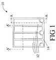
- FIG. 1shows an exemplary flip chip light emitting diode having front-side n-type and p-type electrodes.
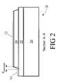
- FIG. 2shows a side sectional view of the flip chip light emitting diode of FIG. 1 along Section A—A.
- FIG. 3shows a side sectional view of the flip chip light emitting diode of FIG. 1 along Section A′—A′.
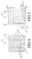
- FIG. 4shows the light emitting diode of FIG. 1 after application of a dielectric layer having vias passing therethrough accessing the n-type and p-type electrodes.
- FIG. 5shows the light emitting diode of FIG. 1 after application of an electrically conductive material defining intermediate connecting pads on the dielectric layer of FIG. 4 .
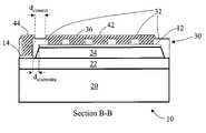
- FIG. 6shows a side sectional view of the flip chip light emitting diode at the processing stage shown in FIG. 5 , along Section B—B.
- FIG. 7shows a side sectional view of the flip chip light emitting diode at the processing stage shown in FIG. 5 , along Section B′—B′.
- FIG. 8shows the light emitting diode of FIG. 1 after application of a second dielectric layer disposed over the intermediate connecting pads shown in FIG. 5 .
- FIG. 9shows the light emitting diode of FIG. 1 after completion of the bonding pads formation process.
- FIG. 10shows a side sectional view of the flip chip light emitting diode with completed bonding pads shown in FIG. 9 , along Section C—C.
- FIG. 11shows a side sectional view of the flip chip light emitting diode with completed bonding pads shown in FIG. 9 , along Section C′—C′.
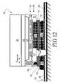
- FIG. 12shows a side sectional view of the flip chip light emitting diode with completed bonding pads shown in FIG. 9 , along Section C—C, after flip chip bonding to a printed circuit board.
- FIG. 13shows a side sectional view of the flip chip light emitting diode with completed bonding pads shown in FIG. 9 , along Section C—C, after additional processing to form a third layer defining bonding pads with a yet larger minimum separation and a higher amount of symmetry.
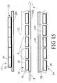
- FIG. 14shows the light emitting diode of FIG. 9 with completed bonding pads formation, in its preferred embodiment as part of a substrate wafer having other light emitting diodes fabricated thereon.
- FIG. 15diagrammatically shows a first preferred processing performed after formation of completed bonding pads but before dicing the substrate wafer of FIG. 14 , in which an encapsulant is applied.
- FIG. 16diagrammatically shows a second preferred processing performed after formation of completed bonding pads but before dicing the substrate wafer of FIG. 14 , in which a phosphor layer is applied and slanted reflective sidewalls are formed.
- a processis described for forming bonding pads on a flip chip light emitting diode 10 in a way which adapts fine features including a small minimum spacing d electrodes between electrodes 12 , 14 of the light emitting diode 10 to a larger tolerance of the flip chip bonding process.
- the exemplary light emitting diode 10 prior to formation of the bonding padsincludes a substrate 20 , an n-type base layer 22 , and one or more device mesas 24 .
- the substrate 20is preferably substantially light transmissive for light generated by the light emitting diode 10 .
- the substrate 20may be thinned to improve light extraction.
- the light emitting diode 10is a group III-nitride based light emitting diode, in which the substrate 20 is sapphire or silicon carbide, the n-type base layer 22 is an n-type gallium nitride layer or an n-type aluminum gallium nitride layer, and the device mesa or mesas 24 include an n-type gallium nitride or aluminum gallium nitride cladding layer adjacent the n-type base layer 22 , an active region adjacent the n-type cladding layer including one or more indium gallium nitride layers, a p-type gallium nitride or aluminum gallium nitride cladding layer adjacent a side of the active region distal from the substrate 20 , and a heavily doped p-type contact-enhancing layer of a group III-nitride material including one or more of indium, gallium, and aluminum adjacent a side of the p-type gallium n
- the exemplary group III-nitride light emitting diode 10optionally includes other layers, such as an epitaxy-enhancing buffer layer of aluminum nitride or another material interposed between the substrate 20 and the n-type base layer 22 .
- Other group III-nitride layerscan be included elsewhere in the epitaxial layers stack to provide other desired structural, electrical, and/or optical effects, such as current spreading, improved electrical conductance, optical confinement, carrier confinement, abrupt interfaces between layers, and the like.
- the light emitting diode 10is suitably formed by heteroepitaxially depositing group III-nitride layers on the substrate 20 and removing selected portions of the deposited layers by lithographic processing to define the device mesa or mesas 24 and to access the n-type material.
- the described group III-nitride light emitting diodeis exemplary only.
- the light emitting diode 10can be constructed using other materials, such as group III-phosphides, group III-arsenides, and the like.
- formation of the bonding padsis described with reference to the exemplary p-on-n light emitting diode 10 , the described bonding pads formation processing is also applicable to n-on-p light emitting diodes.
- the light emitting diode 10is suitably formed by depositing group layers on the substrate 20 and removing material by lithographic processing to define the device mesa or mesas 24 and to expose portions of the n-type base layer 22 .
- the electrodes 12 , 14include one or more p-type electrodes 12 corresponding to and formed on the device mesa or mesas 24 and one or more n-type electrodes 14 formed on exposed portions of the n-type base layer 22 .
- the electrodes 12 , 14are metal stacks, such as a nickel/titanium/gold stack which is suitable for contacting group III-nitride materials. Those skilled in the art can readily select suitable materials or material stacks for the electrodes 12 , 14 .
- the exemplary light emitting diode 10has four generally rectangular device mesas 24 and a corresponding four generally rectangular p-type electrodes 12 .
- the n-type electrode 14is arranged as fingers proximate to the four device mesas 24 .
- Those skilled in the artcan employ other electrode configurations to enhance current spreading or other diode aspects. Note that in FIG. 1 , the small lateral gap d electrodes between the p-type electrodes 12 and the n-type electrode 14 labeled in FIG. 2 is not indicated.
- electroluminescenceis generated in the device mesas 24 by electrical current flowing between the electrodes 12 , 14 .
- the spacing d electrodes between the electrodes 12 , 14is preferably small to reduce resistance to current flow.
- the device mesas 24 and the n-type electrode 14are preferably distributed over the lateral area of the light emitting diode 10 to maximize lateral current spreading across the mesa 24 .
- the n-type electrode fingersare preferably spaced apart by about 0.20 mm to 0.25 mm. As the p-type electrodes 12 are interposed between the n-type electrode fingers, this makes d electrodes less than the fingers spacing.
- the flip chip bondingshould be performed with a lateral tolerance of about 0.15 mm or less. Such a tight tolerance is generally not achievable using existing automated die-attachment tools.
- the bonding pads formation processincludes formation of a fanning layer 30 as shown in FIGS. 4–7 .
- Formation of the fanning layer 30includes depositing a dielectric layer 32 in which vias 34 are formed to provide access to the p-type electrode 12 and the n-type electrode 14 , followed by metallization processing that fills the vias 34 with an electrically conductive material 36 and that forms intermediate connecting pads, specifically an intermediate p-type connecting pad 42 and an intermediate n-type connecting pad 44 .
- the dielectric layer 32preferably hermetically seals the n-type and p-type electrodes 12 , 14 and the front-side of the light emitting diode 10 .
- the hermetic sealingadvantageously allows for optional omission of a separate encapsulant layer during later device packaging.
- FIG. 4shows the light emitting diode 10 after the dielectric layer 32 is disposed thereon and the vias 34 are formed, but before the electrically conductive material 36 is disposed.
- the dielectric layer 32is suitably a polyamide material; however, other materials such as silicon nitride or silicon dioxide can be used,
- the dielectric layer 32 shown in FIG. 4is substantially light transmissive; hence, the lateral structure of the mesas 24 and n-electrode 14 remain visible in FIG.
- the dielectric layer 32is preferably at least 2 microns thick. Depending upon the dielectric and structural characteristics of the dielectric layer 32 , a thinner dielectric layer may be suitable.
- the vias 34are suitably formed by a lithographic processing after blanket deposition of the preferably hermetically sealing dielectric layer 32 .
- lithographic processingcan be used to mask the vias areas during deposition of the dielectric layer 32 , after which the mask is removed leaving the vias 34 .
- the vias 34provide access to the p-type and n-type electrodes 12 , 14 .
- several vias 34 contacting each of the electrodes 12 , 14are distributed across the lateral area of the light emitting diode 10 to promote current spreading across the light emitting diode 10 .
- the electrically conductive material 36can be deposited by vacuum evaporation, sputtering, electroplating, or the like. If an evaporative technique is used, a lateral extent of the intermediate p-type and n-type connecting pads 42 , 44 is defined by lithographic techniques known in the art. For electroplating, a thin seed layer (not shown) is deposited inside the vias 34 and the electrically conductive material 36 is electroplated to fill the vias 34 and to extend outside the vias 34 . Extension or overflowing of the electroplated material outside of the vias is known as “mushrooming” in the art. The electrically conductive material 36 lying outside of the vias 34 defines the connecting pads 42 , 44 .
- a thin adhesion layeris disposed between the electrically conductive material 36 and the electrodes 12 , 14 to promote adhesion.
- a thin diffusion barrier layeris optionally disposed at an interface between the electrically conductive material 36 and the electrodes 12 , 14 to suppress intermixing of the electrically conductive material 36 and the material of the electrodes 12 , 14 .
- a thin titanium and/or nickel layeris deposited on the electrodes 12 , 14 , and the electrically conductive material 36 is gold or silver.
- the portion of the electrically conductive material 36 residing in the vias 34define electrically conductive paths providing electrical communication between the electrodes 12 , 14 and the connecting pads 42 , 44 .
- the connecting pads 42 , 44have a minimum separation d connect that is greater than the minimum electrodes separation d electrodes .
- the intermediate p-type connecting pad 42extends laterally across the dielectric layer 32 to connect the vias that access the p-type electrode 12 and to connect the four device mesas 24 to define a single p-type connecting pad 42 .
- FIG. 5–7the intermediate p-type connecting pad 42 extends laterally across the dielectric layer 32 to connect the vias that access the p-type electrode 12 and to connect the four device mesas 24 to define a single p-type connecting pad 42 .
- the n-type connecting pad 44extends laterally across the dielectric layer 32 to connect the vias that access the n-type electrode 14 to define a single n-type connecting pad 44 .
- the connecting pads 42 , 44are preferably thick enough so that the pads 42 , 44 are not limiting sources of electrical resistance. Pad thicknesses of about a micron or thicker are preferred.
- the connecting pads 42 , 44have a lateral configuration that is advantageously better adapted for flip chip bonding than the lateral configuration of the electrodes 12 , 14 .
- the connecting pads 42 , 44have a simple rectangular geometry that does not follow the complex lateral configuration of the four mesas 24 and the fingers of the n-type electrode 14 .
- bonding bumps on a printed circuit board for die attachmentcan have a correspondingly simple geometry.
- the minimum separation d connect of the connecting pads 42 , 44is larger than the minimum electrodes separation d electrodes .
- the minimum separationis related to the maximum lateral tolerance that can be permitted in the flip chip bonding process, since for a small separation a correspondingly small error in lateral alignment during die attachment can shunt the separation.
- the larger minimum separation d connect of the connecting pads 42 , 44permits larger lateral tolerances in the flip chip bonding process.
- the device as shown in FIGS. 5–7 with the fanning layer 30 disposed on the front-side of the light emitting diode 10is contemplated for direct flip chip bonding without a sub-mount to a printed circuit board, using the connecting pads 42 , 44 as bonding pads.
- the connecting pads 42 , 44are optionally coated with a bonding layer or layers stack (not shown) that promotes soldering, reflow alloy bonding, or another selected bonding method for electrically and mechanically securing the light emitting diode 10 to bonding bumps of a printed circuit board.
- the bonding pads fabrication processis continued to produce a second, bonding pad layer 50 on top of the fanning layer 30 .
- the connecting pads 42 , 44provide a substantial adaptation for direct flip chip bonding of the LED 10 to a printed circuit board without a sub-mount, they have certain deficiencies.
- the vias 34 that communicate between the p-type electrode 12 and the p-type connecting pad 42impose a substantial lateral overlap between the p-type electrode 12 and the p-type connecting pad 42 . This overlap constrains a maximum size of the minimum separation d connect of the connecting pads 42 , 44 .
- the bonding pad layer 50is disposed on a side of the fanning layer 30 that is distal from the electrodes 12 , 14 .
- Formation of the bonding pad layer 50includes deposition of a second dielectric layer 52 in which vias 54 that provide access to the p-type connecting pad 42 and the n-type connecting pad 44 are formed, followed by a metallization process that fills the vias 54 with an electrically conductive material 56 (which may be the same as the electrically conductive material 36 , or which may be different from the electrically conductive material 36 ) and forms bonding pads, specifically a p-type bonding pad 62 and an n-type bonding pad 64 .
- FIG. 8shows the light emitting diode 10 after the second dielectric layer 52 is disposed thereon and the vias 54 are formed, but before disposition of the electrically conductive material 56 .
- the second dielectric layer 52is suitably a polyamide material, although other materials such as silicon nitride or silicon dioxide can be used.
- the second dielectric layer 52 shown in FIG. 8is substantially light transmissive; hence, the intermediate connecting pads 42 , 44 remain visible in FIG. 8 through the second dielectric layer 52 .
- a translucent or opaque dielectric materialcan also be employed.
- the dielectric layer 52is preferably at least 2 microns thick. Depending upon the dielectric and structural characteristics of the dielectric layer 52 , a thinner dielectric layer may be suitable.
- the second dielectric layer 52may be made of the same material as the dielectric layer 32 , or it may be made of a different material.
- the vias 54are suitably formed by a lithographic process after blanket deposition of the second dielectric layer 52 .
- lithographic processingcan be used to mask the vias areas during deposition of the dielectric layer 52 , after which the mask is removed leaving the vias 54 .
- the vias 54provide access to the p-type and n-type intermediate connecting pads 42 , 44 .
- the electrically conductive material 56can be deposited by vacuum evaporation, sputtering, electroplating, or the like. In the case of evaporative techniques, a lateral extent of the intermediate p-type and n-type bonding pads 62 , 64 is defined by lithographic techniques known in the art.
- FIGS. 10 and 11illustrate an electroplating embodiment in which a thin seed layer 66 is deposited inside the vias 54 and the electrically conductive material 56 is electroplated to fill the vias 54 and to mushroom outside the vias 54 to define the bonding pads 62 , 64 .
- Other layerscan be included in the disposing of the electrically conductive material 56 which are not shown in FIGS. 10 and 11 .
- a thin adhesion layer and/or diffusion barrier layeris interposed between the electrically conductive material 56 and the intermediate connecting pads 42 , 44 .
- a thin titanium and/or nickel layeris deposited on the intermediate connecting pads 42 , 44 and the electrically conductive material 56 is gold or silver.
- Those skilled in the artcan readily select other material stacks that control adhesion and intermixing at the interface between the intermediate connecting pads 42 , 44 and the electrically conductive material 56 .
- the portion of the electrically conductive material 56 residing in the vias 54define electrically conductive paths providing electrical communication between the connecting pads 42 , 44 and the bonding pads 62 , 64 .
- the bonding pads 62 , 64have a minimum separation d pads that is greater than the minimum electrodes separation d electrodes and that is greater than the minimum separation d connect of the intermediate connecting pads 42 , 44 .
- the bonding pads 62 , 64are preferably thick enough so that the pads 62 , 64 are not limiting sources of electrical resistance, and are also preferably thick enough to participate in the selected die attach process. Thicknesses of the bonding pads 62 , 64 of about two microns or thicker are preferred, although thinner bonding pads can be employed.
- the bonding pads 62 , 64are coated with a diffusion barrier layer 70 and a reflow layer stack 72 .
- the diffusion barrier layer 70is a nickel layer and the reflow stack 72 is a gold/tin stack having a desired composition.
- the reflow stack 72can be configured as distinct layers, staggered layers, or mixed layers to provide the desired diffusion characteristics during reflow.
- the light emitting diode 10is flip chip bonded to a printed circuit board 76 (partially shown in FIG. 12 ) having printed circuitry including at least positive and negative power traces 80 , 82 on which bonding bumps 86 are disposed.
- the bonding bumpscan be gold- or silver-plated copper bumps, gold bumps, silver bumps, or the like.
- the bonding bumps 86can include multiple layers, such as a stack including an adhesion layer, a diffusion barrier layer, and a bondable layer.
- the bonding bumps 86laterally align with the bonding pads 62 , 64 for flip chip bonding. Die attachment is achieved by reflow alloying of the reflow layer 72 with material of the bonding bumps 86 .
- the reflow alloyingis performed using a heat source such as an infra-red or convection reflow oven, a vapor phase, convection, or hotplate heat source, or the like.
- a heat sourcesuch as an infra-red or convection reflow oven, a vapor phase, convection, or hotplate heat source, or the like.
- the heatingshould elevate the temperature of the reflow stack 72 to greater than about 232° C. corresponding to the tin melting point, to effect reflow alloying.
- the reflowcauses alloying at the interface between the reflow stack 72 and the bonding bumps 86 to form mechanically secure and electrically conductive bonds 72 ′.
- an oxide reducing fluxis advantageously applied to the die attach area to promote the reflow bonding process.
- the flip chip bonding attachmentcan be made using thermo-sonic bonding, ultrasonic bonding, conventional soldering, or the like.
- bonding to the printed circuit board 76is described, the die attach techniques described herein can be used for die attach to substantially any type of substrate, such as a glass substrate, or a substrate of a composite material.
- the preferred process for fabricating bonding pads described with reference to FIGS. 4–11employs two layers, namely the fan layer 30 and the bonding pads layer 50 .
- the bonding pad processingcan be extended to three layers.
- the bonding pad layer 50serves as a second fan layer, and the p-type and n-type bonding pads 62 , 64 serve as a second set of intermediate connecting pads.
- a third layer 90is disposed over the second layer 50 . Formation of the third layer 90 includes depositing a third dielectric layer 92 followed by a metallizing process that fills vias through the dielectric layer 92 accessing the pads 62 , 64 with an electrically conductive material 96 that also extends over the dielectric layer 92 to define exposed p-type and n-type bonding pads 102 , 104 .
- the third layer 90has a minimum bonding pads separation d 3-layer that is even larger than the minimum bonding pads separation d pads of the second layer 50 .
- the bonding pads 102 , 104are advantageously more symmetric with respect to the lateral area of the light emitting diode 10 than are the pads 62 , 64 .
- moving upward from the intermediate p-type connecting pad 42 to the p-type pad 62 which acts as a second intermediate connecting pad to the exposed bonding pad 102the center of the p-type contact region shifts outwardly toward an edge of the light emitting diode 10 .
- the center of the n-type contact regionshifts inwardly from an edge of the light emitting diode 10 . Since the p-type electrode 12 was positioned near the center of the light emitting diode 10 while the n-type electrode 14 was positioned near an edge of the light emitting diode 10 , the result of this shifting is that the exposed bonding pads 102 , 104 are more nearly symmetrically arranged respective to the light emitting diode 10 than are the electrodes 12 , 14 . Such symmetry coupled with the large minimum bonding pads separation d 3-layer accommodates substantial lateral tolerances in the flip chip bonding process.
- each additional layerprovides additional fanning to increase the minimum separation between the n-type and p-type pads.
- Each additional layerprovides additional flexibility in arranging the topmost exposed bonding pads.
- the described processingis readily extended to four or more layers to provide still greater flexibility; however, as fabrication of each layer involves several processes including at least dielectric deposition, lithography to form vias, and metallization, the number of layers is preferably kept small.
- the two layer process whose culmination is shown in FIGS. 9–12is preferred, while the three layer process whose culmination is shown in FIG. 13 may be preferred for use in conjunction with die attachment processes having especially large tolerances.
- FIGS. 1–13illustrate the bonding pads fabrication process applied to a single light emitting diode 10 .
- the described processingis applied at wafer level, with the wafer diced after formation of the pads 42 , 44 (for a one-layer process), or after formation of the bonding pads 62 , 64 (for a two-layer process), or after formation of the bonding pads 102 , 104 (for a three-layer process).
- the substrate 20 of the light emitting diode 10is preferably a portion of a substrate wafer 110 that is shared with other light emitting diodes.
- the substrate wafer 110has a plurality of light emitting diodes fabricated thereon using wafer-level processing, including the exemplary light emitting diode 10 .
- the light emitting diode 10has the bonding pads 62 , 64 (for the exemplary two-layer process) which are fabricated in accordance with the bonding pads fabrication described herein applied as wafer-level processing.
- all the light emitting diodes on the substrate wafer 110have bonding pads corresponding to the bonding pads 62 , 64 .
- the preferred dicing of the substrate wafer 110 after formation of the bonding pads 62 , 64is indicated by dashed die separation lines.
- additional wafer-level processingincluding at least disposition of one or more optical components on the light emitting diode 10 and on the other light emitting diodes of the substrate wafer 110 is performed after formation of the bonding pads 62 , 64 but before the dicing.
- an encapsulant of selected thicknessis applied to the transparent substrate 20 and sidewalls.
- the encapsulantprovides improved light extraction through better index-matching, and optionally provides some refractive focusing.
- FIG. 15shows the processing by diagrammatically showing the substrate wafer 110 along the section D—D indicated in FIG. 14 at three points during the processing.
- the descriptionparticularly focuses on the exemplary light emitting diode 10 .
- the substrate wafer 110is adhered to a stretchable sticky tape 120 in a face-down position, that is, with the bonding pads layer 50 adjacent the sticky tape.
- Dicingis performed from the backside (i.e., from the side of the substrate 20 ) after securing to the tape 120 .
- the dicingis performed using a diamond scribe, laser cutting, or the like.
- a tension force T(diagrammatically indicated by arrows) is applied to the tape 120 to introduce a selected separation S between the dice.
- an encapsulant 122such as an epoxy is applied to the backside of the dice, and also flows into the separations S.
- the encapsulant 122is cured at a low temperature.
- the encapsulated diceare removed from the tensioned stretchable sticky tape 120 and are placed encapsulant-down on a second tape 126 for dicing of the encapsulant.
- the dicing of the encapsulantis indicated by vertical dashed lines in the lower portion of FIG. 15 .
- each diehas a fixed thickness of encapsulant on the backside controlled by the thickness of the deposited encapsulant 122 , and a fixed thickness of encapsulant on the sidewalls controlled by the separation S produced by the tensioning T.
- a phosphor layer of selected thicknessis applied to the transparent substrate 20 , and slanted sidewalls are formed and coated with a reflective coating.
- group III-nitride light emitting diodes producing ultraviolet or blue electroluminescenceare advantageously combined with a white, yellow, or other phosphor to generate substantially white light.
- FIG. 16shows the processing by diagrammatically showing the substrate wafer 110 along the section D—D indicated in FIG. 14 at two points during the processing.
- the descriptionparticularly focuses on the exemplary light emitting diode 10 .
- the substrate wafer 110is initially processed by making wedge-shaped cuts 130 formed from the front-side using a laser or other cutting device.
- a reflective coating 132is disposed in the cuts 130 by electroplating, vacuum evaporation, or the like.
- the waferis then mounted face-down on a wax 136 to provide mechanical support, and the substrate 20 is thinned. This thinning is done as a wafer-level process; that is, a backside of the substrate wafer 110 including the substrate 20 is thinned.
- a phosphor coating 140is applied to the backside and cured at low temperature.
- the wax 136is then removed and the dice are separated at the cuts 130 to isolate, for example, the light emitting diode 10 .
- the resulting devicesare suitable for flip chip bonding as shown in FIG. 12 .
- the reflective coating 132 and the wafer thinningimprove light extraction into the phosphor coating 140
- the phosphor coating 140provides a selected light conversion, for example from ultraviolet to white light for a group III-nitride light emitting diode.
- FIGS. 15 and 16are applied after the bonding pads are fabricated, and are exemplary only. Those skilled in the art can readily modify the exemplary processing sequences for specific applications. It will be appreciated that the processing sequences of FIGS. 15 and 16 are enabled by the hermetic sealing of the front-side of the light emitting diode 10 by the encapsulant 32 , and more generally by the bonding pad layer or layers 30 , 50 , 90 . By forming the bonding pads including hermetic sealing of the front-side before performing the end processing sequences of FIGS. 15 and 16 , wafer-level the end processing can be performed without additional intervening processes for protecting the relatively delicate front surface.
- the front-sideis protected by applying a thick photoresist to the front-side prior to processing.
- Thishas a number of disadvantages, including chemical contamination of the front-side by hydrocarbons or other substances in the photoresist, possible contamination of the processing tools by the photoresist, and additional time and cost of the photoresist application and stripping.
Landscapes
- Led Device Packages (AREA)
Abstract
Description
Claims (32)
Priority Applications (7)
| Application Number | Priority Date | Filing Date | Title |
|---|---|---|---|
| US10/794,935US7179670B2 (en) | 2004-03-05 | 2004-03-05 | Flip-chip light emitting diode device without sub-mount |
| CNA2005800122262ACN1947222A (en) | 2004-03-05 | 2005-02-18 | Flip Chip Light Emitting Diode Device Without Submount |
| JP2007501814AJP5112049B2 (en) | 2004-03-05 | 2005-02-18 | Flip chip light emitting diode element without submount |
| KR1020067020807AKR20060129526A (en) | 2004-03-05 | 2005-02-18 | Flip-chip LED Device without Submount |
| EP05713772AEP1726033A2 (en) | 2004-03-05 | 2005-02-18 | Flip-chip light emitting diode device without sub-mount |
| PCT/US2005/005160WO2005091848A2 (en) | 2004-03-05 | 2005-02-18 | Flip-chip light emitting diode device without sub-mount |
| US11/654,165US20070114557A1 (en) | 2004-03-05 | 2007-01-16 | Flip-chip light emitting diode device without sub-mount |
Applications Claiming Priority (1)
| Application Number | Priority Date | Filing Date | Title |
|---|---|---|---|
| US10/794,935US7179670B2 (en) | 2004-03-05 | 2004-03-05 | Flip-chip light emitting diode device without sub-mount |
Related Child Applications (1)
| Application Number | Title | Priority Date | Filing Date |
|---|---|---|---|
| US11/654,165ContinuationUS20070114557A1 (en) | 2004-03-05 | 2007-01-16 | Flip-chip light emitting diode device without sub-mount |
Publications (2)
| Publication Number | Publication Date |
|---|---|
| US20050194605A1 US20050194605A1 (en) | 2005-09-08 |
| US7179670B2true US7179670B2 (en) | 2007-02-20 |
Family
ID=34912385
Family Applications (2)
| Application Number | Title | Priority Date | Filing Date |
|---|---|---|---|
| US10/794,935Expired - LifetimeUS7179670B2 (en) | 2004-03-05 | 2004-03-05 | Flip-chip light emitting diode device without sub-mount |
| US11/654,165AbandonedUS20070114557A1 (en) | 2004-03-05 | 2007-01-16 | Flip-chip light emitting diode device without sub-mount |
Family Applications After (1)
| Application Number | Title | Priority Date | Filing Date |
|---|---|---|---|
| US11/654,165AbandonedUS20070114557A1 (en) | 2004-03-05 | 2007-01-16 | Flip-chip light emitting diode device without sub-mount |
Country Status (6)
| Country | Link |
|---|---|
| US (2) | US7179670B2 (en) |
| EP (1) | EP1726033A2 (en) |
| JP (1) | JP5112049B2 (en) |
| KR (1) | KR20060129526A (en) |
| CN (1) | CN1947222A (en) |
| WO (1) | WO2005091848A2 (en) |
Cited By (41)
| Publication number | Priority date | Publication date | Assignee | Title |
|---|---|---|---|---|
| US20050152146A1 (en)* | 2002-05-08 | 2005-07-14 | Owen Mark D. | High efficiency solid-state light source and methods of use and manufacture |
| US20050218468A1 (en)* | 2004-03-18 | 2005-10-06 | Owen Mark D | Micro-reflectors on a substrate for high-density LED array |
| US20050231713A1 (en)* | 2004-04-19 | 2005-10-20 | Owen Mark D | Imaging semiconductor structures using solid state illumination |
| US20060001035A1 (en)* | 2004-06-22 | 2006-01-05 | Toyoda Gosei Co., Ltd. | Light emitting element and method of making same |
| US20060189098A1 (en)* | 2005-02-23 | 2006-08-24 | Cree, Inc. | Substrate removal process for high light extraction LEDs |
| US20070030678A1 (en)* | 2003-10-31 | 2007-02-08 | Phoseon Technology, Inc. | Series wiring of highly reliable light sources |
| US20070051964A1 (en)* | 2004-04-12 | 2007-03-08 | Owen Mark D | High density led array |
| US20070072324A1 (en)* | 2005-09-27 | 2007-03-29 | Lumileds Lighting U.S., Llc | Substrate for growing a III-V light emitting device |
| US20070109790A1 (en)* | 2003-10-31 | 2007-05-17 | Phoseon Technology, Inc. | Collection optics for led array with offset hemispherical or faceted surfaces |
| US20070154823A1 (en)* | 2005-12-30 | 2007-07-05 | Phoseon Technology, Inc. | Multi-attribute light effects for use in curing and other applications involving photoreactions and processing |
| US20070278504A1 (en)* | 2002-05-08 | 2007-12-06 | Roland Jasmin | Methods and systems relating to solid state light sources for use in industrial processes |
| US20090212317A1 (en)* | 2008-02-27 | 2009-08-27 | Lumination Llc | Circuit board for direct flip chip attachment |
| US20100171135A1 (en)* | 2007-04-26 | 2010-07-08 | Karl Engl | Optoelectronic Semiconductor Body and Method for Producing the Same |
| US20100207157A1 (en)* | 2005-06-09 | 2010-08-19 | Koninklijke Philips Electronics N.V. | Led assembly having maximum metal support for laser lift-off of growth substrate |
| DE102009039891A1 (en)* | 2009-09-03 | 2011-03-10 | Osram Opto Semiconductors Gmbh | Optoelectronic module having at least a first semiconductor body with a radiation exit side and an insulating layer and method for its production |
| US20110068424A1 (en)* | 2009-09-23 | 2011-03-24 | International Business Machines Corporation | Thick bond pad for chip with cavity package |
| US20110272824A1 (en)* | 2010-05-04 | 2011-11-10 | Stats Chippac, Ltd. | Semiconductor Device and Method of Forming Channels in Back Surface of FO-WLCSP for Heat Dissipation |
| US20110284910A1 (en)* | 2010-05-24 | 2011-11-24 | Kabushiki Kaisha Toshiba | Semiconductor light emitting device |
| US20120091481A1 (en)* | 2010-10-19 | 2012-04-19 | Napra Co., Ltd. | Light-emitting device and method for manufacturing the same |
| US20120241793A1 (en)* | 2011-03-22 | 2012-09-27 | Seoul Opto Device Co., Ltd. | Light emitting diode package and method for manufacturing the same |
| US20130002986A1 (en)* | 2010-05-18 | 2013-01-03 | Sharp Kabushiki Kaisha | Display device |
| US20130134462A1 (en)* | 2010-08-16 | 2013-05-30 | Korea Phototonics Technology Institute | Light emitting diode having multi-cell structure and method of manufacturing the same |
| USD684549S1 (en)* | 2011-10-28 | 2013-06-18 | SemiLEDs Optoelectronics Co., Ltd. | LED chip |
| USD684548S1 (en)* | 2011-10-28 | 2013-06-18 | SemiLEDs Optoelectronics Co., Ltd. | LED chip |
| USD684941S1 (en)* | 2011-10-28 | 2013-06-25 | SemiLEDs Optoelectronics Co., Ltd. | LED chip |
| USD684940S1 (en)* | 2011-10-28 | 2013-06-25 | SemiLEDs Optoelectronics Co., Ltd. | LED chip |
| USD685334S1 (en)* | 2011-10-28 | 2013-07-02 | SemiLEDs Optoelectronics Co., Ltd. | LED chip |
| USD687395S1 (en)* | 2011-10-28 | 2013-08-06 | SemiLEDs Optoelectronics Co., Ltd. | LED chip |
| US8506105B2 (en) | 2010-08-25 | 2013-08-13 | Generla Electric Company | Thermal management systems for solid state lighting and other electronic systems |
| USD689834S1 (en)* | 2011-10-28 | 2013-09-17 | Semileds Opto Electronics Co., Ltd. | LED chip |
| USD690670S1 (en)* | 2011-10-28 | 2013-10-01 | SemiLEDs Optoelectronics Co., Ltd. | LED chip |
| USD693779S1 (en)* | 2011-10-28 | 2013-11-19 | SemiLEDs Optoelectronics Co., Ltd. | LED chip |
| US9219196B2 (en)* | 2010-09-24 | 2015-12-22 | Seoul Semiconductor Co., Ltd. | Wafer-level light emitting diode package and method of fabricating the same |
| US9269858B2 (en)* | 2011-08-31 | 2016-02-23 | Micron Technology, Inc. | Engineered substrates for semiconductor devices and associated systems and methods |
| US9412903B2 (en) | 2014-01-20 | 2016-08-09 | Samsung Electronics Co., Ltd. | Semiconductor light emitting device |
| US9666561B2 (en) | 2015-10-12 | 2017-05-30 | Samsung Electronics Co., Ltd. | Light emitting device package and lighting apparatus including the same |
| US9954028B2 (en) | 2016-08-11 | 2018-04-24 | Samsung Electronics Co., Ltd. | Light emitting device package and display device using the same |
| US10205074B2 (en) | 2015-12-16 | 2019-02-12 | Samsung Electronics Co., Ltd. | Circuit board for mounting of semiconductor light emitting device and semiconductor light emitting device package using the same |
| US10319884B2 (en) | 2011-09-16 | 2019-06-11 | Seoul Viosys Co., Ltd. | Light emitting diode |
| US10580929B2 (en) | 2016-03-30 | 2020-03-03 | Seoul Viosys Co., Ltd. | UV light emitting diode package and light emitting diode module having the same |
| US10644202B2 (en) | 2013-01-10 | 2020-05-05 | Epistar Corporation | Electrode of light-emitting device |
Families Citing this family (122)
| Publication number | Priority date | Publication date | Assignee | Title |
|---|---|---|---|---|
| US10686106B2 (en) | 2003-07-04 | 2020-06-16 | Epistar Corporation | Optoelectronic element |
| US20070126016A1 (en)* | 2005-05-12 | 2007-06-07 | Epistar Corporation | Light emitting device and manufacture method thereof |
| US7462861B2 (en)* | 2004-04-28 | 2008-12-09 | Cree, Inc. | LED bonding structures and methods of fabricating LED bonding structures |
| JP4632690B2 (en)* | 2004-05-11 | 2011-02-16 | スタンレー電気株式会社 | Semiconductor light emitting device and manufacturing method thereof |
| SE527101C2 (en)* | 2004-05-19 | 2005-12-20 | Volvo Lastvagnar Ab | Magnetic circuit breaker arrangement and method for obtaining a differential magnetic circuit breaker |
| TW200541094A (en)* | 2004-06-03 | 2005-12-16 | Yu-Nung Shen | Light-emitting diode wafer package and packaging method thereof |
| TW200637033A (en)* | 2004-11-22 | 2006-10-16 | Matsushita Electric Industrial Co Ltd | Light-emitting device, light-emitting module, display unit, lighting unit and method for manufacturing light-emitting device |
| US20150295154A1 (en) | 2005-02-03 | 2015-10-15 | Epistar Corporation | Light emitting device and manufacturing method thereof |
| US9018655B2 (en) | 2005-02-03 | 2015-04-28 | Epistar Corporation | Light emitting apparatus and manufacture method thereof |
| TWI244228B (en)* | 2005-02-03 | 2005-11-21 | United Epitaxy Co Ltd | Light emitting device and manufacture method thereof |
| JP4778745B2 (en)* | 2005-07-27 | 2011-09-21 | パナソニック株式会社 | Semiconductor light emitting device and manufacturing method thereof |
| US9443903B2 (en)* | 2006-06-30 | 2016-09-13 | Cree, Inc. | Low temperature high strength metal stack for die attachment |
| KR100763345B1 (en)* | 2006-08-30 | 2007-10-04 | 삼성전기주식회사 | Manufacturing Method of Electronic Circuit Board |
| US9111950B2 (en)* | 2006-09-28 | 2015-08-18 | Philips Lumileds Lighting Company, Llc | Process for preparing a semiconductor structure for mounting |
| JP2008258459A (en)* | 2007-04-06 | 2008-10-23 | Toshiba Corp | Light emitting device and manufacturing method thereof |
| JP5045336B2 (en)* | 2007-04-16 | 2012-10-10 | 豊田合成株式会社 | Semiconductor light emitting device |
| JP5216251B2 (en)* | 2007-05-16 | 2013-06-19 | フィリップス ルミレッズ ライティング カンパニー リミテッド ライアビリティ カンパニー | Method for pretreating a semiconductor light emitting device for mounting |
| KR100941766B1 (en)* | 2007-08-08 | 2010-02-11 | 한국광기술원 | Semiconductor light emitting diode using pad rearrangement and manufacturing method thereof |
| US8368100B2 (en)* | 2007-11-14 | 2013-02-05 | Cree, Inc. | Semiconductor light emitting diodes having reflective structures and methods of fabricating same |
| KR101423929B1 (en) | 2007-12-26 | 2014-08-04 | 삼성전자주식회사 | Light Emitting Diode device |
| US8124999B2 (en)* | 2008-07-18 | 2012-02-28 | Toyoda Gosei Co., Ltd. | Light emitting element and method of making the same |
| TW201021240A (en)* | 2008-11-24 | 2010-06-01 | Harvatek Corp | Wafer level LED package structure for increasing light-emitting efficiency |
| JP4724222B2 (en)* | 2008-12-12 | 2011-07-13 | 株式会社東芝 | Method for manufacturing light emitting device |
| TWI422075B (en)* | 2009-03-13 | 2014-01-01 | Advanced Optoelectronic Tech | Structure of flip-chip semiconductor photoelectric element and manufacturing method thereof |
| CN102804415A (en)* | 2009-06-18 | 2012-11-28 | 松下电器产业株式会社 | Gallium nitride-based compound semiconductor light-emitting diode |
| JP5326957B2 (en)* | 2009-09-15 | 2013-10-30 | 豊田合成株式会社 | Light emitting device manufacturing method and light emitting device |
| JP5152133B2 (en)* | 2009-09-18 | 2013-02-27 | 豊田合成株式会社 | Light emitting element |
| JP2011071272A (en)* | 2009-09-25 | 2011-04-07 | Toshiba Corp | Semiconductor light-emitting device and method for manufacturing the same |
| JP5349260B2 (en) | 2009-11-19 | 2013-11-20 | 株式会社東芝 | Semiconductor light emitting device and manufacturing method thereof |
| JP5414579B2 (en)* | 2009-11-19 | 2014-02-12 | 株式会社東芝 | Semiconductor light emitting device |
| JP5197654B2 (en) | 2010-03-09 | 2013-05-15 | 株式会社東芝 | Semiconductor light emitting device and manufacturing method thereof |
| JP2011199193A (en)* | 2010-03-23 | 2011-10-06 | Toshiba Corp | Light emitting device and method of manufacturing the same |
| JP2011199221A (en)* | 2010-03-24 | 2011-10-06 | Hitachi Cable Ltd | Light emitting diode |
| US8604498B2 (en)* | 2010-03-26 | 2013-12-10 | Tsmc Solid State Lighting Ltd. | Single phosphor layer photonic device for generating white light or color lights |
| JP2011233650A (en)* | 2010-04-26 | 2011-11-17 | Toshiba Corp | Semiconductor light-emitting device |
| JP5325834B2 (en)* | 2010-05-24 | 2013-10-23 | 株式会社東芝 | Semiconductor light emitting device and manufacturing method thereof |
| JP5426481B2 (en)* | 2010-05-26 | 2014-02-26 | 株式会社東芝 | Light emitting device |
| JP5281612B2 (en)* | 2010-05-26 | 2013-09-04 | 株式会社東芝 | Semiconductor light emitting device and manufacturing method thereof |
| JP5337105B2 (en)* | 2010-06-03 | 2013-11-06 | 株式会社東芝 | Semiconductor light emitting device |
| JP5390472B2 (en) | 2010-06-03 | 2014-01-15 | 株式会社東芝 | Semiconductor light emitting device and manufacturing method thereof |
| JP5337106B2 (en)* | 2010-06-04 | 2013-11-06 | 株式会社東芝 | Semiconductor light emitting device |
| JP5759790B2 (en)* | 2010-06-07 | 2015-08-05 | 株式会社東芝 | Manufacturing method of semiconductor light emitting device |
| JP5343040B2 (en)* | 2010-06-07 | 2013-11-13 | 株式会社東芝 | Semiconductor light emitting device |
| JP5449039B2 (en)* | 2010-06-07 | 2014-03-19 | 株式会社東芝 | Semiconductor light emitting device and manufacturing method thereof |
| JP5398644B2 (en) | 2010-06-07 | 2014-01-29 | 株式会社東芝 | Light source device using semiconductor light emitting device |
| KR101142965B1 (en)* | 2010-09-24 | 2012-05-08 | 서울반도체 주식회사 | Wafer-level light emitting diode package and method of fabricating the same |
| CN102064164B (en)* | 2010-10-28 | 2012-03-21 | 山东华光光电子有限公司 | Freely combined lamp wick of flip-chip power LED tube core |
| KR20120045919A (en)* | 2010-11-01 | 2012-05-09 | 삼성엘이디 주식회사 | Semiconductor light emitting device |
| JP2012164938A (en)* | 2011-02-09 | 2012-08-30 | Stanley Electric Co Ltd | Method of manufacturing semiconductor light-emitting device |
| JP5603793B2 (en)* | 2011-02-09 | 2014-10-08 | 株式会社東芝 | Semiconductor light emitting device |
| CN102683514B (en)* | 2011-03-06 | 2017-07-14 | 维亚甘有限公司 | LED package and manufacture method |
| JP5603813B2 (en)* | 2011-03-15 | 2014-10-08 | 株式会社東芝 | Semiconductor light emitting device and light emitting device |
| JP5462217B2 (en)* | 2011-05-20 | 2014-04-02 | 株式会社東芝 | Method for manufacturing light emitting device |
| CN103548162B (en) | 2011-05-24 | 2016-11-09 | 皇家飞利浦有限公司 | P-N Separation Metal Filler for Flip Chip LED |
| US9653643B2 (en)* | 2012-04-09 | 2017-05-16 | Cree, Inc. | Wafer level packaging of light emitting diodes (LEDs) |
| US9666764B2 (en) | 2012-04-09 | 2017-05-30 | Cree, Inc. | Wafer level packaging of multiple light emitting diodes (LEDs) on a single carrier die |
| US8896125B2 (en)* | 2011-07-05 | 2014-11-25 | Sony Corporation | Semiconductor device, fabrication method for a semiconductor device and electronic apparatus |
| KR101939333B1 (en)* | 2011-10-07 | 2019-01-16 | 서울바이오시스 주식회사 | Light emitting diode package |
| KR101969334B1 (en)* | 2011-11-16 | 2019-04-17 | 엘지이노텍 주식회사 | Light emitting device and light emitting apparatus having the same |
| TW201336031A (en)* | 2012-02-16 | 2013-09-01 | 矽品精密工業股份有限公司 | Semiconductor package and its manufacturing method |
| US9847445B2 (en)* | 2012-04-05 | 2017-12-19 | Koninklijke Philips N.V. | LED thin-film device partial singulation prior to substrate thinning or removal |
| JPWO2013161208A1 (en)* | 2012-04-27 | 2015-12-21 | パナソニックIpマネジメント株式会社 | Light emitting element |
| JP2013232504A (en)* | 2012-04-27 | 2013-11-14 | Toshiba Corp | Semiconductor light-emitting device |
| JP5989420B2 (en)* | 2012-06-28 | 2016-09-07 | 株式会社東芝 | Semiconductor light emitting device |
| US8816383B2 (en)* | 2012-07-06 | 2014-08-26 | Invensas Corporation | High performance light emitting diode with vias |
| TWI572068B (en) | 2012-12-07 | 2017-02-21 | 晶元光電股份有限公司 | Light-emitting element |
| JP5915504B2 (en)* | 2012-11-06 | 2016-05-11 | 日亜化学工業株式会社 | Semiconductor light emitting device |
| JP2013042191A (en)* | 2012-11-30 | 2013-02-28 | Toshiba Corp | Semiconductor light-emitting device |
| TWI602326B (en)* | 2012-12-07 | 2017-10-11 | 晶元光電股份有限公司 | Light-emitting element |
| JP5462378B2 (en)* | 2013-01-10 | 2014-04-02 | 株式会社東芝 | Semiconductor light emitting device, light emitting device, and method for manufacturing semiconductor light emitting device |
| JP5592963B2 (en)* | 2013-01-30 | 2014-09-17 | 株式会社東芝 | Light source device using semiconductor light emitting device |
| JP5426788B2 (en)* | 2013-01-31 | 2014-02-26 | 株式会社東芝 | Semiconductor light emitting device |
| JP5422760B2 (en)* | 2013-02-04 | 2014-02-19 | 株式会社東芝 | Semiconductor light emitting device |
| US9318674B2 (en)* | 2013-02-05 | 2016-04-19 | Cree, Inc. | Submount-free light emitting diode (LED) components and methods of fabricating same |
| US10439107B2 (en) | 2013-02-05 | 2019-10-08 | Cree, Inc. | Chip with integrated phosphor |
| JP6580299B2 (en)* | 2013-02-12 | 2019-09-25 | 日亜化学工業株式会社 | Light emitting device |
| JP5537700B2 (en)* | 2013-05-23 | 2014-07-02 | 株式会社東芝 | Semiconductor light emitting device |
| JP6180801B2 (en)* | 2013-06-07 | 2017-08-16 | ルネサスエレクトロニクス株式会社 | Semiconductor device |
| JP6136737B2 (en)* | 2013-08-09 | 2017-05-31 | 日亜化学工業株式会社 | Light emitting element |
| US9490173B2 (en)* | 2013-10-30 | 2016-11-08 | Infineon Technologies Ag | Method for processing wafer |
| JP6248604B2 (en)* | 2013-12-18 | 2017-12-20 | 日亜化学工業株式会社 | Semiconductor light emitting device and electrode forming method thereof |
| TWI552386B (en)* | 2013-12-20 | 2016-10-01 | 新世紀光電股份有限公司 | Semiconductor light emitting structure and semiconductor package structure |
| US20150228594A1 (en)* | 2014-02-13 | 2015-08-13 | Qualcomm Incorporated | Via under the interconnect structures for semiconductor devices |
| CN103794689A (en)* | 2014-02-25 | 2014-05-14 | 深圳市兆明芯科技控股有限公司 | Manufacture method of flip chip type light-emitting diode (LED) chip |
| JP5834109B2 (en)* | 2014-05-14 | 2015-12-16 | 株式会社東芝 | Semiconductor light emitting device, method for manufacturing semiconductor light emitting device, and method for manufacturing light emitting device |
| JP6308025B2 (en)* | 2014-05-30 | 2018-04-11 | 日亜化学工業株式会社 | LIGHT EMITTING DEVICE AND LIGHT EMITTING DEVICE MANUFACTURING METHOD |
| KR102407827B1 (en)* | 2015-01-27 | 2022-06-13 | 서울바이오시스 주식회사 | Light emitting device |
| KR102263066B1 (en)* | 2014-11-12 | 2021-06-10 | 서울바이오시스 주식회사 | Light emitting device |
| USD826871S1 (en) | 2014-12-11 | 2018-08-28 | Cree, Inc. | Light emitting diode device |
| JP6019367B2 (en)* | 2015-01-13 | 2016-11-02 | 株式会社野田スクリーン | Semiconductor device |
| TWI583019B (en)* | 2015-02-17 | 2017-05-11 | 新世紀光電股份有限公司 | Light emitting diode and manufacturing method thereof |
| JP6034456B2 (en)* | 2015-07-16 | 2016-11-30 | 株式会社東芝 | Semiconductor light emitting device and light emitting device |
| US10388834B2 (en) | 2015-08-03 | 2019-08-20 | Soko Kagaku Co., Ltd. | Nitride semiconductor wafer, manufacturing method thereof, nitride semiconductor ultraviolet light-emitting element, and nitride semiconductor ultraviolet light-emitting device |
| KR102409964B1 (en)* | 2015-08-04 | 2022-06-16 | 삼성전자주식회사 | Semiconductor light emitting device and method of manufacturing the same |
| TWM542252U (en)* | 2015-10-16 | 2017-05-21 | 首爾偉傲世有限公司 | Small light-emitting diode chip |
| US9851056B2 (en) | 2015-10-16 | 2017-12-26 | Seoul Viosys Co., Ltd. | Compact light emitting diode chip and light emitting device having a slim structure with secured durability |
| KR101894046B1 (en)* | 2016-08-24 | 2018-09-04 | 서울바이오시스 주식회사 | Compact light emitting diode chip and light emitting device including the same |
| US10126831B2 (en) | 2015-10-16 | 2018-11-13 | Seoul Viosys Co., Ltd. | Compact light emitting diode chip, light emitting device and electronic device including the same |
| JP6072192B2 (en)* | 2015-10-22 | 2017-02-01 | 株式会社東芝 | Semiconductor light emitting device, method for manufacturing semiconductor light emitting device, and method for manufacturing light emitting device |
| CN105489744A (en)* | 2016-01-20 | 2016-04-13 | 深圳市聚飞光电股份有限公司 | Flip chip type LED element and manufacturing method thereof |
| KR102550005B1 (en)* | 2016-07-15 | 2023-07-03 | 서울바이오시스 주식회사 | Uv light emitting diode |
| DE102017111123A1 (en)* | 2017-05-22 | 2018-11-22 | Osram Opto Semiconductors Gmbh | Optoelectronic semiconductor chip and method for producing an optoelectronic semiconductor chip |
| DE102017113407A1 (en)* | 2017-06-19 | 2018-12-20 | Osram Opto Semiconductors Gmbh | A radiation-emitting semiconductor chip, a method for producing a radiation-emitting semiconductor chip and a method for producing a radiation-emitting arrangement |
| JP6903087B2 (en)* | 2017-09-26 | 2021-07-14 | 晶元光電股▲ふん▼有限公司Epistar Corporation | Light emitting element |
| JP6501845B2 (en)* | 2017-09-26 | 2019-04-17 | 晶元光電股▲ふん▼有限公司Epistar Corporation | Light emitting element |
| JP2019106406A (en)* | 2017-12-08 | 2019-06-27 | Dowaエレクトロニクス株式会社 | Semiconductor light-emitting element, surface mounting device using the same, and their manufacturing methods |
| US10490428B2 (en) | 2017-12-22 | 2019-11-26 | Lumidleds LLC | Method and system for dual stretching of wafers for isolated segmented chip scale packages |
| US10141475B1 (en)* | 2017-12-24 | 2018-11-27 | Mikro Mesa Technology Co., Ltd. | Method for binding micro device to conductive pad |
| US20190378963A1 (en)* | 2018-06-06 | 2019-12-12 | Advanced Semiconductor Engineering, Inc. | Electronic apparatus and method for manufacturing the same |
| KR102001663B1 (en)* | 2018-08-23 | 2019-07-18 | 서울바이오시스 주식회사 | Light emitting diode package |
| JP7336451B2 (en) | 2018-09-13 | 2023-08-31 | ヌヴォトンテクノロジージャパン株式会社 | semiconductor light emitting device |
| JP6806218B2 (en)* | 2018-10-31 | 2021-01-06 | 日亜化学工業株式会社 | Light emitting device, light emitting module, light emitting device and manufacturing method of light emitting module |
| JP7312789B2 (en)* | 2019-03-19 | 2023-07-21 | 晶元光電股▲ふん▼有限公司 | light emitting element |
| US10959336B2 (en)* | 2019-03-28 | 2021-03-23 | Mikro Mesa Technology Co., Ltd. | Method of liquid assisted binding |
| US10986737B2 (en)* | 2019-03-28 | 2021-04-20 | Mikro Mesa Technology Co., Ltd. | Method of restricting micro device on conductive pad |
| CN111916419B (en)* | 2019-05-08 | 2024-01-09 | 菲尼萨公司 | Electrical coupling fitting and method for an optoelectronic module |
| CN112185988B (en)* | 2019-06-17 | 2022-12-06 | 成都辰显光电有限公司 | Display panel and method for preparing display panel |
| KR102149911B1 (en)* | 2019-11-25 | 2020-08-31 | 서울바이오시스 주식회사 | Light emitting diode and led module having the same |
| WO2021142346A1 (en) | 2020-01-08 | 2021-07-15 | Avicenatech Corp. | Packaging for microleds for chip to chip communication |
| EP4122011A4 (en)* | 2020-03-18 | 2024-07-03 | Avicenatech Corp. | Led array for in-plane optical interconnects |
| JP6839320B1 (en)* | 2020-05-13 | 2021-03-03 | 日機装株式会社 | Semiconductor light emitting element and manufacturing method of semiconductor light emitting element |
| TWI787890B (en)* | 2021-06-30 | 2022-12-21 | 錼創顯示科技股份有限公司 | Micro light-emitting diode display device |
Citations (18)
| Publication number | Priority date | Publication date | Assignee | Title |
|---|---|---|---|---|
| US5795619A (en) | 1995-12-13 | 1998-08-18 | National Science Council | Solder bump fabricated method incorporate with electroless deposit and dip solder |
| US6153503A (en) | 1997-03-10 | 2000-11-28 | National Science Council | Continuous process for producing solder bumps on electrodes of semiconductor chips |
| US6222207B1 (en) | 1999-05-24 | 2001-04-24 | Lumileds Lighting, U.S. Llc | Diffusion barrier for increased mirror reflectivity in reflective solderable contacts on high power LED chip |
| US6268114B1 (en) | 1998-09-18 | 2001-07-31 | Taiwan Semiconductor Manufacturing Company, Ltd | Method for forming fine-pitched solder bumps |
| US6307218B1 (en) | 1998-11-20 | 2001-10-23 | Lumileds Lighting, U.S., Llc | Electrode structures for light emitting devices |
| US6326701B1 (en)* | 1999-02-24 | 2001-12-04 | Sanyo Electric Co., Ltd. | Chip size package and manufacturing method thereof |
| US6440836B1 (en) | 1999-03-16 | 2002-08-27 | Industrial Technology Research Institute | Method for forming solder bumps on flip chips and devices formed |
| US20020179901A1 (en)* | 2001-06-01 | 2002-12-05 | Semiconductor Energy Laboratory Co., Ltd. | Organic semiconductor device and process of manufacturing the same |
| US6514782B1 (en) | 1999-12-22 | 2003-02-04 | Lumileds Lighting, U.S., Llc | Method of making a III-nitride light-emitting device with increased light generating capability |
| US6521914B2 (en)* | 1999-12-22 | 2003-02-18 | Lumileds Lighting, U.S., Llc | III-Nitride Light-emitting device with increased light generating capability |
| US6547249B2 (en) | 2001-03-29 | 2003-04-15 | Lumileds Lighting U.S., Llc | Monolithic series/parallel led arrays formed on highly resistive substrates |
| US6573537B1 (en) | 1999-12-22 | 2003-06-03 | Lumileds Lighting, U.S., Llc | Highly reflective ohmic contacts to III-nitride flip-chip LEDs |
| US20030151148A1 (en)* | 2000-11-06 | 2003-08-14 | St Assembly Test Services Pte Ltd | Single unit automated assembly of flex enhanced ball grid array packages |
| US20030190770A1 (en) | 2002-04-09 | 2003-10-09 | Oriol, Inc. | Method of etching substrates |
| US6656828B1 (en) | 1999-01-22 | 2003-12-02 | Hitachi, Ltd. | Method of forming bump electrodes |
| US6661029B1 (en) | 2000-03-31 | 2003-12-09 | General Electric Company | Color tunable organic electroluminescent light source |
| US6924437B1 (en)* | 2003-04-10 | 2005-08-02 | Cisco Technology, Inc. | Techniques for coupling an object to a circuit board using a surface mount coupling device |
| US6969626B2 (en) | 2004-02-05 | 2005-11-29 | Advanced Epitaxy Technology | Method for forming LED by a substrate removal process |
Family Cites Families (6)
| Publication number | Priority date | Publication date | Assignee | Title |
|---|---|---|---|---|
| JP2003017757A (en)* | 2001-06-29 | 2003-01-17 | Sanken Electric Co Ltd | Flip-chip semiconductor light emitting element |
| JP4214704B2 (en)* | 2002-03-20 | 2009-01-28 | 日亜化学工業株式会社 | Semiconductor element |
| JP4580633B2 (en)* | 2003-11-14 | 2010-11-17 | スタンレー電気株式会社 | Semiconductor device and manufacturing method thereof |
| KR20070041411A (en)* | 2004-07-12 | 2007-04-18 | 로무 가부시키가이샤 | Semiconductor light emitting device |
| US7402831B2 (en)* | 2004-12-09 | 2008-07-22 | 3M Innovative Properties Company | Adapting short-wavelength LED's for polychromatic, broadband, or “white” emission |
| KR100708936B1 (en)* | 2005-10-17 | 2007-04-17 | 삼성전기주식회사 | Nitride-based semiconductor light emitting device for flip chip |
- 2004
- 2004-03-05USUS10/794,935patent/US7179670B2/ennot_activeExpired - Lifetime
- 2005
- 2005-02-18JPJP2007501814Apatent/JP5112049B2/ennot_activeExpired - Fee Related
- 2005-02-18WOPCT/US2005/005160patent/WO2005091848A2/enactiveApplication Filing
- 2005-02-18KRKR1020067020807Apatent/KR20060129526A/ennot_activeWithdrawn
- 2005-02-18CNCNA2005800122262Apatent/CN1947222A/enactivePending
- 2005-02-18EPEP05713772Apatent/EP1726033A2/ennot_activeWithdrawn
- 2007
- 2007-01-16USUS11/654,165patent/US20070114557A1/ennot_activeAbandoned
Patent Citations (20)
| Publication number | Priority date | Publication date | Assignee | Title |
|---|---|---|---|---|
| US5795619A (en) | 1995-12-13 | 1998-08-18 | National Science Council | Solder bump fabricated method incorporate with electroless deposit and dip solder |
| US6153503A (en) | 1997-03-10 | 2000-11-28 | National Science Council | Continuous process for producing solder bumps on electrodes of semiconductor chips |
| US6268114B1 (en) | 1998-09-18 | 2001-07-31 | Taiwan Semiconductor Manufacturing Company, Ltd | Method for forming fine-pitched solder bumps |
| US6307218B1 (en) | 1998-11-20 | 2001-10-23 | Lumileds Lighting, U.S., Llc | Electrode structures for light emitting devices |
| US6656828B1 (en) | 1999-01-22 | 2003-12-02 | Hitachi, Ltd. | Method of forming bump electrodes |
| US6326701B1 (en)* | 1999-02-24 | 2001-12-04 | Sanyo Electric Co., Ltd. | Chip size package and manufacturing method thereof |
| US6440836B1 (en) | 1999-03-16 | 2002-08-27 | Industrial Technology Research Institute | Method for forming solder bumps on flip chips and devices formed |
| US6222207B1 (en) | 1999-05-24 | 2001-04-24 | Lumileds Lighting, U.S. Llc | Diffusion barrier for increased mirror reflectivity in reflective solderable contacts on high power LED chip |
| US20010004534A1 (en) | 1999-05-24 | 2001-06-21 | Carrie Carter-Coman | Diffusion barrier for increased mirror reflectivity in reflective solderable contacts on high power led chip |
| US6514782B1 (en) | 1999-12-22 | 2003-02-04 | Lumileds Lighting, U.S., Llc | Method of making a III-nitride light-emitting device with increased light generating capability |
| US6521914B2 (en)* | 1999-12-22 | 2003-02-18 | Lumileds Lighting, U.S., Llc | III-Nitride Light-emitting device with increased light generating capability |
| US6573537B1 (en) | 1999-12-22 | 2003-06-03 | Lumileds Lighting, U.S., Llc | Highly reflective ohmic contacts to III-nitride flip-chip LEDs |
| US6661029B1 (en) | 2000-03-31 | 2003-12-09 | General Electric Company | Color tunable organic electroluminescent light source |
| US20030151148A1 (en)* | 2000-11-06 | 2003-08-14 | St Assembly Test Services Pte Ltd | Single unit automated assembly of flex enhanced ball grid array packages |
| US6547249B2 (en) | 2001-03-29 | 2003-04-15 | Lumileds Lighting U.S., Llc | Monolithic series/parallel led arrays formed on highly resistive substrates |
| US20020179901A1 (en)* | 2001-06-01 | 2002-12-05 | Semiconductor Energy Laboratory Co., Ltd. | Organic semiconductor device and process of manufacturing the same |
| US20030190770A1 (en) | 2002-04-09 | 2003-10-09 | Oriol, Inc. | Method of etching substrates |
| US6924437B1 (en)* | 2003-04-10 | 2005-08-02 | Cisco Technology, Inc. | Techniques for coupling an object to a circuit board using a surface mount coupling device |
| US6969626B2 (en) | 2004-02-05 | 2005-11-29 | Advanced Epitaxy Technology | Method for forming LED by a substrate removal process |
| US7026181B2 (en) | 2004-02-05 | 2006-04-11 | Advanced Epitaxy Technology | Method for forming LED by a substrate removal process |
Cited By (83)
| Publication number | Priority date | Publication date | Assignee | Title |
|---|---|---|---|---|
| US8192053B2 (en) | 2002-05-08 | 2012-06-05 | Phoseon Technology, Inc. | High efficiency solid-state light source and methods of use and manufacture |
| US8496356B2 (en) | 2002-05-08 | 2013-07-30 | Phoseon Technology, Inc. | High efficiency solid-state light source and methods of use and manufacture |
| US10401012B2 (en) | 2002-05-08 | 2019-09-03 | Phoseon Technology, Inc. | High efficiency solid-state light source and methods of use and manufacture |
| US20050152146A1 (en)* | 2002-05-08 | 2005-07-14 | Owen Mark D. | High efficiency solid-state light source and methods of use and manufacture |
| US7461949B2 (en) | 2002-05-08 | 2008-12-09 | Phoseon Technology, Inc. | Methods and systems relating to solid state light sources for use in industrial processes |
| US20070278504A1 (en)* | 2002-05-08 | 2007-12-06 | Roland Jasmin | Methods and systems relating to solid state light sources for use in industrial processes |
| US8523387B2 (en) | 2003-10-31 | 2013-09-03 | Phoseon Technology, Inc. | Collection optics for LED array with offset hemispherical or faceted surfaces |
| US7524085B2 (en) | 2003-10-31 | 2009-04-28 | Phoseon Technology, Inc. | Series wiring of highly reliable light sources |
| US20070109790A1 (en)* | 2003-10-31 | 2007-05-17 | Phoseon Technology, Inc. | Collection optics for led array with offset hemispherical or faceted surfaces |
| US7819550B2 (en) | 2003-10-31 | 2010-10-26 | Phoseon Technology, Inc. | Collection optics for led array with offset hemispherical or faceted surfaces |
| US20070030678A1 (en)* | 2003-10-31 | 2007-02-08 | Phoseon Technology, Inc. | Series wiring of highly reliable light sources |
| US20110063840A1 (en)* | 2003-10-31 | 2011-03-17 | Phoseon Technology, Inc. | Collection optics for led array with offset hemispherical or faceted surfaces |
| US20050218468A1 (en)* | 2004-03-18 | 2005-10-06 | Owen Mark D | Micro-reflectors on a substrate for high-density LED array |
| US7638808B2 (en) | 2004-03-18 | 2009-12-29 | Phoseon Technology, Inc. | Micro-reflectors on a substrate for high-density LED array |
| US8637332B2 (en) | 2004-03-18 | 2014-01-28 | Phoseon Technology, Inc. | Micro-reflectors on a substrate for high-density LED array |
| US20070051964A1 (en)* | 2004-04-12 | 2007-03-08 | Owen Mark D | High density led array |
| US8077305B2 (en) | 2004-04-19 | 2011-12-13 | Owen Mark D | Imaging semiconductor structures using solid state illumination |
| US20050231713A1 (en)* | 2004-04-19 | 2005-10-20 | Owen Mark D | Imaging semiconductor structures using solid state illumination |
| US20060001035A1 (en)* | 2004-06-22 | 2006-01-05 | Toyoda Gosei Co., Ltd. | Light emitting element and method of making same |
| US20090233003A1 (en)* | 2004-11-08 | 2009-09-17 | Phoseon Technology, Inc. | Methods and systems relating to light sources for use in industrial processes |
| US9281001B2 (en) | 2004-11-08 | 2016-03-08 | Phoseon Technology, Inc. | Methods and systems relating to light sources for use in industrial processes |
| US20060189098A1 (en)* | 2005-02-23 | 2006-08-24 | Cree, Inc. | Substrate removal process for high light extraction LEDs |
| US9559252B2 (en) | 2005-02-23 | 2017-01-31 | Cree, Inc. | Substrate removal process for high light extraction LEDs |
| US7932111B2 (en)* | 2005-02-23 | 2011-04-26 | Cree, Inc. | Substrate removal process for high light extraction LEDs |
| US20100207157A1 (en)* | 2005-06-09 | 2010-08-19 | Koninklijke Philips Electronics N.V. | Led assembly having maximum metal support for laser lift-off of growth substrate |
| US8384118B2 (en)* | 2005-06-09 | 2013-02-26 | Koninklijke Philips Electronics N.V. | LED assembly having maximum metal support for laser lift-off of growth substrate |
| US20070072324A1 (en)* | 2005-09-27 | 2007-03-29 | Lumileds Lighting U.S., Llc | Substrate for growing a III-V light emitting device |
| US8334155B2 (en)* | 2005-09-27 | 2012-12-18 | Philips Lumileds Lighting Company Llc | Substrate for growing a III-V light emitting device |
| US20110027975A1 (en)* | 2005-09-27 | 2011-02-03 | Koninklijke Philips Electronics N.V. | Substrate for growing a iii-v light emitting device |
| US8288186B2 (en) | 2005-09-27 | 2012-10-16 | Philips Lumileds Lighting Company Llc | Substrate for growing a III-V light emitting device |
| US7642527B2 (en) | 2005-12-30 | 2010-01-05 | Phoseon Technology, Inc. | Multi-attribute light effects for use in curing and other applications involving photoreactions and processing |
| US20070154823A1 (en)* | 2005-12-30 | 2007-07-05 | Phoseon Technology, Inc. | Multi-attribute light effects for use in curing and other applications involving photoreactions and processing |
| US8653540B2 (en) | 2007-04-26 | 2014-02-18 | Osram Opto Semiconductors Gmbh | Optoelectronic semiconductor body and method for producing the same |
| US20100171135A1 (en)* | 2007-04-26 | 2010-07-08 | Karl Engl | Optoelectronic Semiconductor Body and Method for Producing the Same |
| US8450751B2 (en) | 2007-04-26 | 2013-05-28 | Osram Opto Semiconductors Gmbh | Optoelectronic semiconductor body and method for producing the same |
| US7749813B2 (en) | 2008-02-27 | 2010-07-06 | Lumination Llc | Circuit board for direct flip chip attachment |
| US20090212317A1 (en)* | 2008-02-27 | 2009-08-27 | Lumination Llc | Circuit board for direct flip chip attachment |
| US8847247B2 (en) | 2009-09-03 | 2014-09-30 | Osram Opto Semiconductors Gmbh | Optoelectronic module comprising at least one first semiconductor body having a radiation outlet side and an insulation layer and method for the production thereof |
| DE102009039891A1 (en)* | 2009-09-03 | 2011-03-10 | Osram Opto Semiconductors Gmbh | Optoelectronic module having at least a first semiconductor body with a radiation exit side and an insulating layer and method for its production |
| US8450822B2 (en) | 2009-09-23 | 2013-05-28 | International Business Machines Corporation | Thick bond pad for chip with cavity package |
| US20110068424A1 (en)* | 2009-09-23 | 2011-03-24 | International Business Machines Corporation | Thick bond pad for chip with cavity package |
| US9059180B2 (en) | 2009-09-23 | 2015-06-16 | International Business Machines Corporation | Thick bond pad for chip with cavity package |
| US20110272824A1 (en)* | 2010-05-04 | 2011-11-10 | Stats Chippac, Ltd. | Semiconductor Device and Method of Forming Channels in Back Surface of FO-WLCSP for Heat Dissipation |
| US9431316B2 (en)* | 2010-05-04 | 2016-08-30 | STATS ChipPAC Pte. Ltd. | Semiconductor device and method of forming channels in back surface of FO-WLCSP for heat dissipation |
| US20130002986A1 (en)* | 2010-05-18 | 2013-01-03 | Sharp Kabushiki Kaisha | Display device |
| US20110284910A1 (en)* | 2010-05-24 | 2011-11-24 | Kabushiki Kaisha Toshiba | Semiconductor light emitting device |
| US8729592B2 (en)* | 2010-05-24 | 2014-05-20 | Kabushiki Kaisha Toshiba | Semiconductor light emitting device |
| US20130134462A1 (en)* | 2010-08-16 | 2013-05-30 | Korea Phototonics Technology Institute | Light emitting diode having multi-cell structure and method of manufacturing the same |
| US8710520B2 (en)* | 2010-08-16 | 2014-04-29 | Korea Photonics Technology Institute | Light emitting diode having multi-cell structure and method of manufacturing the same |
| US8506105B2 (en) | 2010-08-25 | 2013-08-13 | Generla Electric Company | Thermal management systems for solid state lighting and other electronic systems |
| US10879437B2 (en) | 2010-09-24 | 2020-12-29 | Seoul Semiconductor Co., Ltd. | Wafer-level light emitting diode package and method of fabricating the same |
| US9882102B2 (en) | 2010-09-24 | 2018-01-30 | Seoul Semiconductor Co., Ltd. | Wafer-level light emitting diode and wafer-level light emitting diode package |
| US9219196B2 (en)* | 2010-09-24 | 2015-12-22 | Seoul Semiconductor Co., Ltd. | Wafer-level light emitting diode package and method of fabricating the same |
| US10069048B2 (en) | 2010-09-24 | 2018-09-04 | Seoul Viosys Co., Ltd. | Wafer-level light emitting diode package and method of fabricating the same |
| US9543490B2 (en) | 2010-09-24 | 2017-01-10 | Seoul Semiconductor Co., Ltd. | Wafer-level light emitting diode package and method of fabricating the same |
| US10892386B2 (en) | 2010-09-24 | 2021-01-12 | Seoul Semiconductor Co., Ltd. | Wafer-level light emitting diode package and method of fabricating the same |
| US8766312B2 (en)* | 2010-10-19 | 2014-07-01 | Napra Co., Ltd. | Light-emitting device comprising vertical conductors and through electrodes and method for manufacturing the same |
| US20120091481A1 (en)* | 2010-10-19 | 2012-04-19 | Napra Co., Ltd. | Light-emitting device and method for manufacturing the same |
| US20120241793A1 (en)* | 2011-03-22 | 2012-09-27 | Seoul Opto Device Co., Ltd. | Light emitting diode package and method for manufacturing the same |
| US10074778B2 (en)* | 2011-03-22 | 2018-09-11 | Seoul Viosys Co., Ltd. | Light emitting diode package and method for manufacturing the same |
| US20190019923A1 (en)* | 2011-03-22 | 2019-01-17 | Seoul Viosys Co., Ltd | Light emitting diode package and method of manufacturing the same |
| US10727376B2 (en) | 2011-03-22 | 2020-07-28 | Seoul Viosys Co., Ltd. | Light emitting diode package and method of manufacturing the same |
| US11563152B2 (en) | 2011-03-22 | 2023-01-24 | Seoul Viosys Co., Ltd. | Light emitting diode package and method of manufacturing the same |
| US12107195B2 (en) | 2011-03-22 | 2024-10-01 | Seoul Viosys Co., Ltd. | Light emitting diode package and method of manufacturing the same |
| US9269858B2 (en)* | 2011-08-31 | 2016-02-23 | Micron Technology, Inc. | Engineered substrates for semiconductor devices and associated systems and methods |
| US10319884B2 (en) | 2011-09-16 | 2019-06-11 | Seoul Viosys Co., Ltd. | Light emitting diode |
| US10756237B2 (en) | 2011-09-16 | 2020-08-25 | Seoul Viosys Co., Ltd. | Light emitting diode and light emitting diode package |
| US10439105B2 (en) | 2011-09-16 | 2019-10-08 | Seoul Viosys Co., Ltd. | Light emitting diode and light emitting diode package |
| USD687395S1 (en)* | 2011-10-28 | 2013-08-06 | SemiLEDs Optoelectronics Co., Ltd. | LED chip |
| USD690670S1 (en)* | 2011-10-28 | 2013-10-01 | SemiLEDs Optoelectronics Co., Ltd. | LED chip |
| USD689834S1 (en)* | 2011-10-28 | 2013-09-17 | Semileds Opto Electronics Co., Ltd. | LED chip |
| USD684549S1 (en)* | 2011-10-28 | 2013-06-18 | SemiLEDs Optoelectronics Co., Ltd. | LED chip |
| USD693779S1 (en)* | 2011-10-28 | 2013-11-19 | SemiLEDs Optoelectronics Co., Ltd. | LED chip |
| USD684548S1 (en)* | 2011-10-28 | 2013-06-18 | SemiLEDs Optoelectronics Co., Ltd. | LED chip |
| USD684941S1 (en)* | 2011-10-28 | 2013-06-25 | SemiLEDs Optoelectronics Co., Ltd. | LED chip |
| USD684940S1 (en)* | 2011-10-28 | 2013-06-25 | SemiLEDs Optoelectronics Co., Ltd. | LED chip |
| USD685334S1 (en)* | 2011-10-28 | 2013-07-02 | SemiLEDs Optoelectronics Co., Ltd. | LED chip |
| US10644202B2 (en) | 2013-01-10 | 2020-05-05 | Epistar Corporation | Electrode of light-emitting device |
| US9412903B2 (en) | 2014-01-20 | 2016-08-09 | Samsung Electronics Co., Ltd. | Semiconductor light emitting device |
| US9666561B2 (en) | 2015-10-12 | 2017-05-30 | Samsung Electronics Co., Ltd. | Light emitting device package and lighting apparatus including the same |
| US10205074B2 (en) | 2015-12-16 | 2019-02-12 | Samsung Electronics Co., Ltd. | Circuit board for mounting of semiconductor light emitting device and semiconductor light emitting device package using the same |
| US10580929B2 (en) | 2016-03-30 | 2020-03-03 | Seoul Viosys Co., Ltd. | UV light emitting diode package and light emitting diode module having the same |
| US9954028B2 (en) | 2016-08-11 | 2018-04-24 | Samsung Electronics Co., Ltd. | Light emitting device package and display device using the same |
Also Published As
| Publication number | Publication date |
|---|---|
| KR20060129526A (en) | 2006-12-15 |
| US20070114557A1 (en) | 2007-05-24 |
| JP5112049B2 (en) | 2013-01-09 |
| WO2005091848A3 (en) | 2006-01-19 |
| US20050194605A1 (en) | 2005-09-08 |
| EP1726033A2 (en) | 2006-11-29 |
| CN1947222A (en) | 2007-04-11 |
| WO2005091848A2 (en) | 2005-10-06 |
| JP2007527123A (en) | 2007-09-20 |
Similar Documents
| Publication | Publication Date | Title |
|---|---|---|
| US7179670B2 (en) | Flip-chip light emitting diode device without sub-mount | |
| US7589351B2 (en) | Light-emitting device | |
| US7736945B2 (en) | LED assembly having maximum metal support for laser lift-off of growth substrate | |
| US9368428B2 (en) | Dielectric wafer level bonding with conductive feed-throughs for electrical connection and thermal management | |
| CN103180979B (en) | Light-emitting diode chip, light-emitting diode package structure, and forming method thereof | |
| CN101743648B (en) | Substrate removal during LED formation | |
| US9006005B2 (en) | Flip light emitting diode chip and method of fabricating the same | |
| CN105702832B (en) | Carrier for luminescent device | |
| CN101276807B (en) | Semiconductor device and method of manufacturing the same | |
| KR20050021503A (en) | Light emitting diode including barrier layers and manufacturing methods therefor | |
| CN101032034A (en) | Chip-scale methods for packaging light emitting devices and chip-scale packaged light emitting devices | |
| CN101350381A (en) | Salient point LED and manufacturing method thereof | |
| JPH10326806A (en) | Semiconductor device and its manufacture | |
| CN104756267A (en) | Light emitting device, method for manufacturing same, and body having light emitting device mounted thereon | |
| US10651336B2 (en) | Light-emitting device | |
| JP2008181932A (en) | Light emitting device and manufacturing method thereof | |
| CN106663732A (en) | Flip chip led package | |
| JP2012015437A (en) | Semiconductor light-emitting device | |
| JP2000216439A (en) | Chip-type light emitting element and its manufacture | |
| TW201225227A (en) | Method for manufacturing heat dissipation bulk of semiconductor device | |
| TWI397200B (en) | Light-emitting diode device, and package structure and manufacturing method thereof | |
| US11398589B2 (en) | Light emitting device package and light source device | |
| WO2016186667A1 (en) | Led module and related fabrication methods | |
| US20150099319A1 (en) | LED Package with Slanting Structure and Method of the Same | |
| US20240421278A1 (en) | Semiconductor light emitting device and method for manufacturing the same |
Legal Events
| Date | Code | Title | Description |
|---|---|---|---|
| AS | Assignment | Owner name:GELCORE, LLC, OHIO Free format text:ASSIGNMENT OF ASSIGNORS INTEREST;ASSIGNORS:SHELTON, BRYAN S.;LIBON, SEBASTIEN;VENUGOPALAN, HARI S.;AND OTHERS;REEL/FRAME:015055/0831;SIGNING DATES FROM 20040107 TO 20040204 | |
| STCF | Information on status: patent grant | Free format text:PATENTED CASE | |
| FPAY | Fee payment | Year of fee payment:4 | |
| FPAY | Fee payment | Year of fee payment:8 | |
| FEPP | Fee payment procedure | Free format text:11.5 YR SURCHARGE- LATE PMT W/IN 6 MO, LARGE ENTITY (ORIGINAL EVENT CODE: M1556); ENTITY STATUS OF PATENT OWNER: LARGE ENTITY | |
| MAFP | Maintenance fee payment | Free format text:PAYMENT OF MAINTENANCE FEE, 12TH YEAR, LARGE ENTITY (ORIGINAL EVENT CODE: M1553); ENTITY STATUS OF PATENT OWNER: LARGE ENTITY Year of fee payment:12 | |
| AS | Assignment | Owner name:GE LIGHTING SOLUTIONS, LLC, OHIO Free format text:CHANGE OF NAME;ASSIGNOR:LUMINATION, LLC;REEL/FRAME:061354/0832 Effective date:20100721 Owner name:LUMINATION, LLC, OHIO Free format text:CHANGE OF NAME;ASSIGNOR:GELCORE, LLC;REEL/FRAME:061354/0738 Effective date:20070122 Owner name:CURRENT LIGHTING SOLUTIONS, LLC, OHIO Free format text:CHANGE OF NAME;ASSIGNOR:GE LIGHTING SOLUTIONS, LLC;REEL/FRAME:061354/0814 Effective date:20190401 | |
| AS | Assignment | Owner name:CURRENT LIGHTING SOLUTIONS, LLC, OHIO Free format text:PARTIAL RELEASE OF SECURITY INTEREST REEL/FRAME 059034/0469;ASSIGNOR:ATLANTIC PARK STRATEGIC CAPITAL FUND, L.P., AS AGENT;REEL/FRAME:061538/0925 Effective date:20220920 Owner name:CURRENT LIGHTING SOLUTIONS, LLC, OHIO Free format text:RELEASE BY SECURED PARTY;ASSIGNOR:ALLY BANK;REEL/FRAME:061216/0844 Effective date:20220919 | |
| AS | Assignment | Owner name:PROLIGHT OPTO TECHNOLOGY CORPORATION, TAIWAN Free format text:ASSIGNMENT OF ASSIGNORS INTEREST;ASSIGNOR:CURRENT LIGHTNING SOLUTIONS INC.;REEL/FRAME:061341/0789 Effective date:20220912 |