US7178994B2 - Fiber optic circuit connector - Google Patents
Fiber optic circuit connectorDownload PDFInfo
- Publication number
- US7178994B2 US7178994B2US11/311,616US31161605AUS7178994B2US 7178994 B2US7178994 B2US 7178994B2US 31161605 AUS31161605 AUS 31161605AUS 7178994 B2US7178994 B2US 7178994B2
- Authority
- US
- United States
- Prior art keywords
- optical
- right angle
- circuit board
- interface body
- angle interface
- Prior art date
- Legal status (The legal status is an assumption and is not a legal conclusion. Google has not performed a legal analysis and makes no representation as to the accuracy of the status listed.)
- Expired - Fee Related
Links
Images


Classifications
- G—PHYSICS
- G02—OPTICS
- G02B—OPTICAL ELEMENTS, SYSTEMS OR APPARATUS
- G02B6/00—Light guides; Structural details of arrangements comprising light guides and other optical elements, e.g. couplings
- G02B6/24—Coupling light guides
- G02B6/36—Mechanical coupling means
- G02B6/38—Mechanical coupling means having fibre to fibre mating means
- G02B6/3807—Dismountable connectors, i.e. comprising plugs
- G02B6/3833—Details of mounting fibres in ferrules; Assembly methods; Manufacture
- G02B6/3847—Details of mounting fibres in ferrules; Assembly methods; Manufacture with means preventing fibre end damage, e.g. recessed fibre surfaces
- G02B6/3849—Details of mounting fibres in ferrules; Assembly methods; Manufacture with means preventing fibre end damage, e.g. recessed fibre surfaces using mechanical protective elements, e.g. caps, hoods, sealing membranes
- G—PHYSICS
- G02—OPTICS
- G02B—OPTICAL ELEMENTS, SYSTEMS OR APPARATUS
- G02B6/00—Light guides; Structural details of arrangements comprising light guides and other optical elements, e.g. couplings
- G02B6/24—Coupling light guides
- G02B6/36—Mechanical coupling means
- G02B6/38—Mechanical coupling means having fibre to fibre mating means
- G02B6/3807—Dismountable connectors, i.e. comprising plugs
- G02B6/381—Dismountable connectors, i.e. comprising plugs of the ferrule type, e.g. fibre ends embedded in ferrules, connecting a pair of fibres
- G02B6/3825—Dismountable connectors, i.e. comprising plugs of the ferrule type, e.g. fibre ends embedded in ferrules, connecting a pair of fibres with an intermediate part, e.g. adapter, receptacle, linking two plugs
- G—PHYSICS
- G02—OPTICS
- G02B—OPTICAL ELEMENTS, SYSTEMS OR APPARATUS
- G02B6/00—Light guides; Structural details of arrangements comprising light guides and other optical elements, e.g. couplings
- G02B6/24—Coupling light guides
- G02B6/36—Mechanical coupling means
- G02B6/38—Mechanical coupling means having fibre to fibre mating means
- G02B6/3807—Dismountable connectors, i.e. comprising plugs
- G02B6/3897—Connectors fixed to housings, casing, frames or circuit boards
- G—PHYSICS
- G02—OPTICS
- G02B—OPTICAL ELEMENTS, SYSTEMS OR APPARATUS
- G02B6/00—Light guides; Structural details of arrangements comprising light guides and other optical elements, e.g. couplings
- G02B6/24—Coupling light guides
- G02B6/42—Coupling light guides with opto-electronic elements
- G02B6/43—Arrangements comprising a plurality of opto-electronic elements and associated optical interconnections
- H—ELECTRICITY
- H05—ELECTRIC TECHNIQUES NOT OTHERWISE PROVIDED FOR
- H05K—PRINTED CIRCUITS; CASINGS OR CONSTRUCTIONAL DETAILS OF ELECTRIC APPARATUS; MANUFACTURE OF ASSEMBLAGES OF ELECTRICAL COMPONENTS
- H05K1/00—Printed circuits
- H05K1/02—Details
- H05K1/0274—Optical details, e.g. printed circuits comprising integral optical means
- H—ELECTRICITY
- H05—ELECTRIC TECHNIQUES NOT OTHERWISE PROVIDED FOR
- H05K—PRINTED CIRCUITS; CASINGS OR CONSTRUCTIONAL DETAILS OF ELECTRIC APPARATUS; MANUFACTURE OF ASSEMBLAGES OF ELECTRICAL COMPONENTS
- H05K2201/00—Indexing scheme relating to printed circuits covered by H05K1/00
- H05K2201/09—Shape and layout
- H05K2201/09009—Substrate related
- H05K2201/09063—Holes or slots in insulating substrate not used for electrical connections
- H—ELECTRICITY
- H05—ELECTRIC TECHNIQUES NOT OTHERWISE PROVIDED FOR
- H05K—PRINTED CIRCUITS; CASINGS OR CONSTRUCTIONAL DETAILS OF ELECTRIC APPARATUS; MANUFACTURE OF ASSEMBLAGES OF ELECTRICAL COMPONENTS
- H05K2203/00—Indexing scheme relating to apparatus or processes for manufacturing printed circuits covered by H05K3/00
- H05K2203/16—Inspection; Monitoring; Aligning
- H05K2203/167—Using mechanical means for positioning, alignment or registration, e.g. using rod-in-hole alignment
Definitions
- Another aspect of the present inventionis a method for forming an electro-optical multilayer circuit board having embedded optical connectors.
- An additional aspect of the present inventionis an electro-optical back plane having both electrical connectors and optical connectors.
- the electro-optical back planeincludes a fiber management system formed of plural optical fibers, an electrical bus circuit, and a board, wherein the fiber management system and the electrical bus circuit are embedded inside the board.
- the electro-optical back planefurther includes plural optical connectors disposed on the board, each of the optical connectors being coupled to one or more of the plural optical fibers of the fiber management system.
- the electro-optical back planeincludes plural electrical connectors disposed on the board, each of the electrical connectors being electrically connected to the electrical bus circuit.
- the housing parts of the optical connectorare preferably formed of a high Tg material.
- Polyetherimide resinsand in particular ULTEM® resin (a product of GE), have been found to be a suitable as housing material to embody the invention.
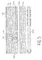
- FIG. 5an initial pre-assembly schematic view is illustrated, showing the relative position of various lamination layers for composing the multi-layer printed circuit board.
- One layeris an electrical inner layer 502 according to known prior art practices.
- a registration plate 504is provided to keep the board structure flat and having alignment holes to align and fix the optical connector during bonding.
- a prepreg layer 506 for bonding and embedding optical management structuresis provided above the laminate layer 504 .
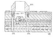
- About the right angle interface body 530.
- a laminate layer 508is provided with the perimeter of the fiber management system 540 being routed out to compensate for thickness differences.
- An adhesive copper tape 512is layered onto the top surface of the right angle interface body 530 to protect the glass fibers, alignment holes, and other surrounding structures from later processing steps.
- the copper tape 512is adhered to the top surface of the right angle interface body 530 by an adhesive.
- the adhesivecan withstand a temperature of at least 210° C. and will not leave behind excessive residue when the copper tape 512 is later removed.
- an outer copper foil 510is layered on as a top layer.
- the outer copper foil 510is preferably about 18 micrometers in thickness.
- the right angle interface body 530has angled sidewalls 531 .
- These angled sidewalls 531serve a dual purpose.
- One reason for having the angles sidewalls 531is to facilitate cleaning around the interface body 530 with a laser that is used to ablate away the board layers above the interface body 530 .
- the second useful purpose for the angled sidewallsis to provide for good alignment with the female connector portion.
- the multilayer printed circuit board 600is shown after machining steps have been conducted on the board. Holes 602 have been drilled through the board 600 for connecting the female connector portion 920 to the surface of the board. A hole 604 has been machined into the upper surface of the board 600 and so is to expose the right angle interface body 530 .
- the outer copper foil layer 510has also been etched to provide conductive runs. At this time the copper tape 512 on the top of the right angle interface body 530 may be pealed off and the top surface of the right angle interface body cleaned 530 .
- the protective copper tape 512is left on the top surface of the right angle interface body 530 until the board 600 has been electrically tested and finally inspected.
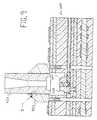
- An anchor body 822is securely engaged to the surface of the board 600 by inserting its anchors 824 into the holes 602 drilled in the board 600 .
- a female self-alignment body 924is forced downward through the anchor body 822 and into the machined out hole 604 in the board 600 until it aligns with the imbedded right angle alignment body 530 .
- FIG. 10a detail view of the interface between the anchor body 822 and the female self-alignment body 924 is illustrated.
- the anchor body 822engages the female self-alignment body 924 via a one way ratchet 926 .
- the fully assembled optical connector 1100is illustrated in a partial section view.
- a male self-alignment body 910is inserted down into the female self-alignment body 920 (formed by the combination of the anchor body 822 and the female self-alignment body 924 ) to guide the male connected portion into precise registration with the top surface of the right angle alignment body 530 .
- the alignment pins 914 of the male connector portion 910are engaged with the precision machined holes 538 of the right angle alignment body 530 .
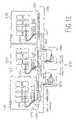
- an electro-optical back plane 1200according to an embodiment of the present invention is illustrated.
- the back plane 1200has an optical carrier 1210 (preferably a fiber management system) embedded with a number of optical connectors 1220 according to embodiments of the present invention.
- optical connectors 1220are placed adjacent to electrical connectors 1222 .
- the printed circuit boards 1230are engaged with the electro-optical back plane 1200 using separate fibers 1224 on the board 1230 slotted into the electro optical back plane 1200 via both the electrical connectors 1222 and their corresponding optical connectors 1220 .
- Purely optical devices 1250may also be plugged into the back plane 1200 .
- an optical switch 1252is shown being connected to optical connectors 1220 alone, as is a splitter coupler device 1254 .
Landscapes
- Physics & Mathematics (AREA)
- General Physics & Mathematics (AREA)
- Optics & Photonics (AREA)
- Engineering & Computer Science (AREA)
- Microelectronics & Electronic Packaging (AREA)
- Optical Couplings Of Light Guides (AREA)
Abstract
Description
Claims (5)
Priority Applications (2)
| Application Number | Priority Date | Filing Date | Title |
|---|---|---|---|
| US11/311,616US7178994B2 (en) | 2000-10-31 | 2005-12-19 | Fiber optic circuit connector |
| US11/703,445US20070172177A1 (en) | 2000-10-31 | 2007-02-07 | Fiber optic circuit connector |
Applications Claiming Priority (4)
| Application Number | Priority Date | Filing Date | Title |
|---|---|---|---|
| US24439000P | 2000-10-31 | 2000-10-31 | |
| US10/051,418US6848840B2 (en) | 2000-10-31 | 2001-10-30 | Fiber optic circuit board connector |
| US10/825,980US6976793B2 (en) | 2000-10-31 | 2004-04-16 | Fiber optic circuit connector |
| US11/311,616US7178994B2 (en) | 2000-10-31 | 2005-12-19 | Fiber optic circuit connector |
Related Parent Applications (1)
| Application Number | Title | Priority Date | Filing Date |
|---|---|---|---|
| US10/825,980ContinuationUS6976793B2 (en) | 2000-10-31 | 2004-04-16 | Fiber optic circuit connector |
Related Child Applications (1)
| Application Number | Title | Priority Date | Filing Date |
|---|---|---|---|
| US11/703,445ContinuationUS20070172177A1 (en) | 2000-10-31 | 2007-02-07 | Fiber optic circuit connector |
Publications (2)
| Publication Number | Publication Date |
|---|---|
| US20060098914A1 US20060098914A1 (en) | 2006-05-11 |
| US7178994B2true US7178994B2 (en) | 2007-02-20 |
Family
ID=36316409
Family Applications (2)
| Application Number | Title | Priority Date | Filing Date |
|---|---|---|---|
| US11/311,616Expired - Fee RelatedUS7178994B2 (en) | 2000-10-31 | 2005-12-19 | Fiber optic circuit connector |
| US11/703,445AbandonedUS20070172177A1 (en) | 2000-10-31 | 2007-02-07 | Fiber optic circuit connector |
Family Applications After (1)
| Application Number | Title | Priority Date | Filing Date |
|---|---|---|---|
| US11/703,445AbandonedUS20070172177A1 (en) | 2000-10-31 | 2007-02-07 | Fiber optic circuit connector |
Country Status (1)
| Country | Link |
|---|---|
| US (2) | US7178994B2 (en) |
Cited By (10)
| Publication number | Priority date | Publication date | Assignee | Title |
|---|---|---|---|---|
| US20060120673A1 (en)* | 2002-08-02 | 2006-06-08 | Morlion Danny L C | Optical connector assembly, coupling device and method for aligning such a coupling device and a waveguide structure |
| US20060222302A1 (en)* | 2005-03-31 | 2006-10-05 | Frank Levinson | Power and communication interface for sensors using a single tethered fiber |
| US20060250276A1 (en)* | 2005-03-31 | 2006-11-09 | Finisar Corporation | Systems and methods for collecting data with sensors |
| US20070172177A1 (en)* | 2000-10-31 | 2007-07-26 | Tourne Joseph A | Fiber optic circuit connector |
| US20070201808A1 (en)* | 2004-04-20 | 2007-08-30 | Deutsch Uk | Waveguide Assembly And Connector |
| US20090169155A1 (en)* | 2007-12-28 | 2009-07-02 | Industrial Technology Research Institute | Optical intermediary component and optical daughter card module |
| US20110206379A1 (en)* | 2010-02-25 | 2011-08-25 | International Business Machines Corporation | Opto-electronic module with improved low power, high speed electrical signal integrity |
| US20130272647A1 (en)* | 2010-09-14 | 2013-10-17 | Fci | Optical coupling device, opticalsystem and methods of assembly |
| US11067755B2 (en)* | 2018-03-08 | 2021-07-20 | Kohoku Kogyo Co., Ltd. | Optical fiber module and method for manufacturing the same |
| US20220029320A1 (en)* | 2018-11-28 | 2022-01-27 | Fujikura Ltd. | Cable and image transmission system |
Families Citing this family (9)
| Publication number | Priority date | Publication date | Assignee | Title |
|---|---|---|---|---|
| US9417418B2 (en) | 2011-09-12 | 2016-08-16 | Commscope Technologies Llc | Flexible lensed optical interconnect device for signal distribution |
| US9229172B2 (en)* | 2011-09-12 | 2016-01-05 | Commscope Technologies Llc | Bend-limited flexible optical interconnect device for signal distribution |
| CN104272155B (en)* | 2012-04-30 | 2016-08-24 | 惠普发展公司,有限责任合伙企业 | Optics basic unit and the equipment of calculating |
| RU2654358C2 (en) | 2012-09-28 | 2018-05-17 | Тайко Электроникс Юк Лтд. | Fiber optic cassette |
| US9223094B2 (en) | 2012-10-05 | 2015-12-29 | Tyco Electronics Nederland Bv | Flexible optical circuit, cassettes, and methods |
| CN109906395B (en) | 2016-09-08 | 2021-06-18 | 康普连通比利时私人有限公司 | Telecom Distribution Components |
| US11409068B2 (en) | 2017-10-02 | 2022-08-09 | Commscope Technologies Llc | Fiber optic circuit and preparation method |
| US11071199B2 (en)* | 2018-10-09 | 2021-07-20 | City University Of Hong Kong | Optical printed circuit board and its fabrication method |
| WO2021202700A1 (en) | 2020-03-31 | 2021-10-07 | Commscope Technologies Llc | Fiber optic cable management systems and methods |
Citations (34)
| Publication number | Priority date | Publication date | Assignee | Title |
|---|---|---|---|---|
| US4184740A (en) | 1976-10-01 | 1980-01-22 | Thomson-Csf | Multi-channel coupler for fibres optic links |
| US4465333A (en)* | 1982-01-15 | 1984-08-14 | Grumman Aerospace Corporation | Electro-optical plug-in interconnection |
| US4496215A (en)* | 1982-09-23 | 1985-01-29 | Rockwell International Corporation | Fiber optic cable |
| US4658130A (en) | 1985-03-22 | 1987-04-14 | Durbin John R | Fiber optic swivel coupler and method of use therefor |
| US4678264A (en)* | 1983-03-30 | 1987-07-07 | Amp Incorporated | Electrical and fiber optic connector assembly |
| US4753510A (en) | 1985-04-11 | 1988-06-28 | Sezerman Omur M | Tilt adjustable optical fibre connectors |
| US4813760A (en)* | 1985-02-26 | 1989-03-21 | E. I. Du Pont De Nemours And Company | Optical connector and plugs therefor |
| US4945400A (en)* | 1988-03-03 | 1990-07-31 | At&T Bell Laboratories | Subassembly for optoelectronic devices |
| US4993803A (en) | 1989-05-18 | 1991-02-19 | General Motors Corporation | Electro-optical header connector |
| EP0454502A1 (en) | 1990-04-27 | 1991-10-30 | Ngk Insulators, Ltd. | Optical circuitry, substrates therefor, opto-electronic devices and methods of making them |
| US5163109A (en) | 1988-10-27 | 1992-11-10 | Kabushiki Kaisha Komatsu Seisakusho | Optical connector assembly |
| US5233677A (en)* | 1992-02-27 | 1993-08-03 | Hughes Aircraft Company | Fiber optic package |
| US5355429A (en)* | 1992-12-30 | 1994-10-11 | Minnesota Mining And Manufacturing Company | Optical fiber strain relief apparatus |
| EP0677757A1 (en) | 1994-04-15 | 1995-10-18 | Jacques Nozick | Connector adaptable to standard pre-wiring, for communication system |
| US5810048A (en) | 1996-08-21 | 1998-09-22 | Zeiner-Gundersen; Dag H. | Metal face sealing coupling |
| WO1999000806A2 (en) | 1997-06-27 | 1999-01-07 | Kolb Elektro Sbw Ag | Method for carrying out an electrical installation and kit for said installation |
| WO1999045421A2 (en) | 1998-03-06 | 1999-09-10 | Telefonaktiebolaget Lm Ericsson (Publ) | A method of fabricating mirrors in polymer waveguides |
| US6004043A (en) | 1997-12-19 | 1999-12-21 | The Whitaker Corporation | Shuttered connector receptacle |
| US6229942B1 (en)* | 1997-02-18 | 2001-05-08 | Telefonaktiebolaget Lm Ericsson (Publ) | Flexfoils having connector tabs |
| US6234688B1 (en) | 1999-05-19 | 2001-05-22 | Trw Inc. | Packaged integrated, actively aligned with sub-micron accuracy single mode fiber optic connector bulkhead receptacle |
| US6257771B1 (en) | 1996-10-17 | 2001-07-10 | Advantest Corporation | Opitcal/electrical hybrid wiring board and its manufacturing method |
| US6343171B1 (en)* | 1998-10-09 | 2002-01-29 | Fujitsu Limited | Systems based on opto-electronic substrates with electrical and optical interconnections and methods for making |
| US6402395B1 (en) | 1998-10-05 | 2002-06-11 | Framatome Connectors International | Optical waveguide plug connector for a mechanically releasable connection between an OWG connector and a printed circuit board |
| US6402389B1 (en)* | 1996-05-03 | 2002-06-11 | Telefonaktiebolaget Lm Ericsson (Publ) | Angled opto-mechanical device |
| US6422761B1 (en)* | 2000-03-06 | 2002-07-23 | Fci Americas Technology, Inc. | Angled optical connector |
| US20020150343A1 (en) | 2001-04-14 | 2002-10-17 | Chiu Liew C. | De-latching mechanisms for fiber optic modules |
| US20020176671A1 (en) | 2000-10-31 | 2002-11-28 | Tourne Joseph A.A.M. | Fiber optic circuit board connector |
| US6490392B1 (en)* | 1999-04-01 | 2002-12-03 | Sony Corporation | Optical transmission system |
| US20030085452A1 (en) | 2001-11-05 | 2003-05-08 | International Business Machines Corporation | Packaging architecture for a multiple array transceiver using a continuous flexible circuit |
| US20040005134A1 (en) | 2002-07-02 | 2004-01-08 | Ke-Xun Sun | Apparatus for cleaning optical fiber connectors and fiber optic parts |
| US20040008964A1 (en)* | 2001-06-26 | 2004-01-15 | Tourne Joseph A.A.M. | Bending an optical fiber into backplane |
| US6694068B2 (en) | 2000-11-17 | 2004-02-17 | Viasystems Technologies Corp. | PCB embedded and surface mounted optical distribution systems |
| US6771860B2 (en) | 2001-06-29 | 2004-08-03 | Xanoptix, Inc. | Module mounted aligning optical connector |
| US7033084B2 (en)* | 2002-08-23 | 2006-04-25 | Erni Elektroapparate Gmbh | Plug-in connector between a circuit board and a back plane |
Family Cites Families (6)
| Publication number | Priority date | Publication date | Assignee | Title |
|---|---|---|---|---|
| US5521992A (en)* | 1994-08-01 | 1996-05-28 | Motorola, Inc. | Molded optical interconnect |
| JP3715425B2 (en)* | 1998-03-06 | 2005-11-09 | ブラザー工業株式会社 | Manufacturing method of substrate with optical waveguide |
| US6785447B2 (en)* | 1998-10-09 | 2004-08-31 | Fujitsu Limited | Single and multilayer waveguides and fabrication process |
| US6845184B1 (en)* | 1998-10-09 | 2005-01-18 | Fujitsu Limited | Multi-layer opto-electronic substrates with electrical and optical interconnections and methods for making |
| US6343177B1 (en)* | 1999-03-26 | 2002-01-29 | Datex-Ohmeda, Inc. | Over-molded reflective optical fiber terminal |
| US7178994B2 (en)* | 2000-10-31 | 2007-02-20 | Viasystems Group, Inc. | Fiber optic circuit connector |
- 2005
- 2005-12-19USUS11/311,616patent/US7178994B2/ennot_activeExpired - Fee Related
- 2007
- 2007-02-07USUS11/703,445patent/US20070172177A1/ennot_activeAbandoned
Patent Citations (35)
| Publication number | Priority date | Publication date | Assignee | Title |
|---|---|---|---|---|
| US4184740A (en) | 1976-10-01 | 1980-01-22 | Thomson-Csf | Multi-channel coupler for fibres optic links |
| US4465333A (en)* | 1982-01-15 | 1984-08-14 | Grumman Aerospace Corporation | Electro-optical plug-in interconnection |
| US4496215A (en)* | 1982-09-23 | 1985-01-29 | Rockwell International Corporation | Fiber optic cable |
| US4678264A (en)* | 1983-03-30 | 1987-07-07 | Amp Incorporated | Electrical and fiber optic connector assembly |
| US4813760A (en)* | 1985-02-26 | 1989-03-21 | E. I. Du Pont De Nemours And Company | Optical connector and plugs therefor |
| US4658130A (en) | 1985-03-22 | 1987-04-14 | Durbin John R | Fiber optic swivel coupler and method of use therefor |
| US4753510A (en) | 1985-04-11 | 1988-06-28 | Sezerman Omur M | Tilt adjustable optical fibre connectors |
| US4945400A (en)* | 1988-03-03 | 1990-07-31 | At&T Bell Laboratories | Subassembly for optoelectronic devices |
| US5163109A (en) | 1988-10-27 | 1992-11-10 | Kabushiki Kaisha Komatsu Seisakusho | Optical connector assembly |
| US4993803A (en) | 1989-05-18 | 1991-02-19 | General Motors Corporation | Electro-optical header connector |
| EP0454502A1 (en) | 1990-04-27 | 1991-10-30 | Ngk Insulators, Ltd. | Optical circuitry, substrates therefor, opto-electronic devices and methods of making them |
| US5233677A (en)* | 1992-02-27 | 1993-08-03 | Hughes Aircraft Company | Fiber optic package |
| US5355429A (en)* | 1992-12-30 | 1994-10-11 | Minnesota Mining And Manufacturing Company | Optical fiber strain relief apparatus |
| EP0677757A1 (en) | 1994-04-15 | 1995-10-18 | Jacques Nozick | Connector adaptable to standard pre-wiring, for communication system |
| US6402389B1 (en)* | 1996-05-03 | 2002-06-11 | Telefonaktiebolaget Lm Ericsson (Publ) | Angled opto-mechanical device |
| US5810048A (en) | 1996-08-21 | 1998-09-22 | Zeiner-Gundersen; Dag H. | Metal face sealing coupling |
| US6257771B1 (en) | 1996-10-17 | 2001-07-10 | Advantest Corporation | Opitcal/electrical hybrid wiring board and its manufacturing method |
| US6229942B1 (en)* | 1997-02-18 | 2001-05-08 | Telefonaktiebolaget Lm Ericsson (Publ) | Flexfoils having connector tabs |
| WO1999000806A2 (en) | 1997-06-27 | 1999-01-07 | Kolb Elektro Sbw Ag | Method for carrying out an electrical installation and kit for said installation |
| US6004043A (en) | 1997-12-19 | 1999-12-21 | The Whitaker Corporation | Shuttered connector receptacle |
| WO1999045421A2 (en) | 1998-03-06 | 1999-09-10 | Telefonaktiebolaget Lm Ericsson (Publ) | A method of fabricating mirrors in polymer waveguides |
| US6402395B1 (en) | 1998-10-05 | 2002-06-11 | Framatome Connectors International | Optical waveguide plug connector for a mechanically releasable connection between an OWG connector and a printed circuit board |
| US6343171B1 (en)* | 1998-10-09 | 2002-01-29 | Fujitsu Limited | Systems based on opto-electronic substrates with electrical and optical interconnections and methods for making |
| US6490392B1 (en)* | 1999-04-01 | 2002-12-03 | Sony Corporation | Optical transmission system |
| US6234688B1 (en) | 1999-05-19 | 2001-05-22 | Trw Inc. | Packaged integrated, actively aligned with sub-micron accuracy single mode fiber optic connector bulkhead receptacle |
| US6422761B1 (en)* | 2000-03-06 | 2002-07-23 | Fci Americas Technology, Inc. | Angled optical connector |
| US20020176671A1 (en) | 2000-10-31 | 2002-11-28 | Tourne Joseph A.A.M. | Fiber optic circuit board connector |
| US6694068B2 (en) | 2000-11-17 | 2004-02-17 | Viasystems Technologies Corp. | PCB embedded and surface mounted optical distribution systems |
| US20020150343A1 (en) | 2001-04-14 | 2002-10-17 | Chiu Liew C. | De-latching mechanisms for fiber optic modules |
| US20040008964A1 (en)* | 2001-06-26 | 2004-01-15 | Tourne Joseph A.A.M. | Bending an optical fiber into backplane |
| US6782181B2 (en)* | 2001-06-26 | 2004-08-24 | Viasystems Group, Inc. | Bending an optical fiber into backplane |
| US6771860B2 (en) | 2001-06-29 | 2004-08-03 | Xanoptix, Inc. | Module mounted aligning optical connector |
| US20030085452A1 (en) | 2001-11-05 | 2003-05-08 | International Business Machines Corporation | Packaging architecture for a multiple array transceiver using a continuous flexible circuit |
| US20040005134A1 (en) | 2002-07-02 | 2004-01-08 | Ke-Xun Sun | Apparatus for cleaning optical fiber connectors and fiber optic parts |
| US7033084B2 (en)* | 2002-08-23 | 2006-04-25 | Erni Elektroapparate Gmbh | Plug-in connector between a circuit board and a back plane |
Non-Patent Citations (3)
| Title |
|---|
| Japanese Publication No. 02 087107, publication date-Mar. 28, 1990, Application date-Sep. 26, 1998, Title: Substrate with Optical Connector, English language abstract attached. |
| Japanese Publication No. 2000-249873, publication date-Sep. 14, 2000, Application date-Feb. 25, 1999, Title: Electronic Circuit Integrated Optical Transmission Module and Its Production, English language abstract attached. |
| Picard A., et al., High Precision LIGA Structures for Optical Fibre-In-Board Technology, pp. 77-80, Jan. 31, 1996. |
Cited By (15)
| Publication number | Priority date | Publication date | Assignee | Title |
|---|---|---|---|---|
| US20070172177A1 (en)* | 2000-10-31 | 2007-07-26 | Tourne Joseph A | Fiber optic circuit connector |
| US7346242B2 (en)* | 2002-08-02 | 2008-03-18 | Fci | Optical connector assembly, coupling device and method for aligning such a coupling device and a waveguide structure |
| US20060120673A1 (en)* | 2002-08-02 | 2006-06-08 | Morlion Danny L C | Optical connector assembly, coupling device and method for aligning such a coupling device and a waveguide structure |
| US7664364B2 (en)* | 2004-04-20 | 2010-02-16 | Deutsch Uk | Waveguide assembly and connector |
| US20070201808A1 (en)* | 2004-04-20 | 2007-08-30 | Deutsch Uk | Waveguide Assembly And Connector |
| US7859071B2 (en)* | 2005-03-31 | 2010-12-28 | Finisar Corporation | Power and communication interface for sensors using a single tethered fiber |
| US20060250276A1 (en)* | 2005-03-31 | 2006-11-09 | Finisar Corporation | Systems and methods for collecting data with sensors |
| US20060222302A1 (en)* | 2005-03-31 | 2006-10-05 | Frank Levinson | Power and communication interface for sensors using a single tethered fiber |
| US8154414B2 (en) | 2005-03-31 | 2012-04-10 | Finisar Corporation | Systems and methods for collecting data with sensors |
| US20090169155A1 (en)* | 2007-12-28 | 2009-07-02 | Industrial Technology Research Institute | Optical intermediary component and optical daughter card module |
| US7627215B2 (en)* | 2007-12-28 | 2009-12-01 | Industrial Technology Research Institute | Optical intermediary component and optical daughter card module |
| US20110206379A1 (en)* | 2010-02-25 | 2011-08-25 | International Business Machines Corporation | Opto-electronic module with improved low power, high speed electrical signal integrity |
| US20130272647A1 (en)* | 2010-09-14 | 2013-10-17 | Fci | Optical coupling device, opticalsystem and methods of assembly |
| US11067755B2 (en)* | 2018-03-08 | 2021-07-20 | Kohoku Kogyo Co., Ltd. | Optical fiber module and method for manufacturing the same |
| US20220029320A1 (en)* | 2018-11-28 | 2022-01-27 | Fujikura Ltd. | Cable and image transmission system |
Also Published As
| Publication number | Publication date |
|---|---|
| US20060098914A1 (en) | 2006-05-11 |
| US20070172177A1 (en) | 2007-07-26 |
Similar Documents
| Publication | Publication Date | Title |
|---|---|---|
| US6976793B2 (en) | Fiber optic circuit connector | |
| US20070172177A1 (en) | Fiber optic circuit connector | |
| AU2002248276A1 (en) | Fiber optic circuit board connector | |
| US6808317B2 (en) | Parallel fiber optics communications module | |
| US7292756B2 (en) | Optical interface assembly and method of formation | |
| US7097365B2 (en) | Transceiver assembly for use in fiber optics communications | |
| US6676302B2 (en) | Method of constructing a fiber optics communications module | |
| KR100871251B1 (en) | Optical module | |
| JP2001141964A (en) | Optical components | |
| US7173192B1 (en) | Position fixing in printed circuit boards | |
| US7073955B1 (en) | Transceiver assembly for use in fiber optics communications | |
| US20030031431A1 (en) | Assembly for aligning an optical array with optical fibers | |
| EP1500961A2 (en) | Fiberoptic circuit board and method of forming an optical connection thereof by embedding an optical interface | |
| HK1072985A (en) | Fiberoptic circuit board and method of forming an optical connection thereof by embedding an optical interface | |
| US7073954B1 (en) | Transceiver assembly for use in fiber optics communications |
Legal Events
| Date | Code | Title | Description |
|---|---|---|---|
| FEPP | Fee payment procedure | Free format text:PAYOR NUMBER ASSIGNED (ORIGINAL EVENT CODE: ASPN); ENTITY STATUS OF PATENT OWNER: LARGE ENTITY | |
| AS | Assignment | Owner name:VIASYSTEMS GROUP, INC., MISSOURI Free format text:ASSIGNMENT OF ASSIGNORS INTEREST;ASSIGNOR:TOURNE, JOSEPH A.A.M.;REEL/FRAME:023848/0023 Effective date:20050104 | |
| AS | Assignment | Owner name:VIASYSTEMS, INC.,MISSOURI Free format text:ASSIGNMENT OF ASSIGNORS INTEREST;ASSIGNOR:VIASYSTEMS GROUP, INC.;REEL/FRAME:023905/0147 Effective date:20100205 | |
| FPAY | Fee payment | Year of fee payment:4 | |
| AS | Assignment | Owner name:WACHOVIA CAPITAL FINANCE CORPORATION (NEW ENGLAND) Free format text:SECURITY AGREEMENT;ASSIGNOR:VIASYSTEMS, INC.;REEL/FRAME:024062/0634 Effective date:20100216 | |
| AS | Assignment | Owner name:WILMINGTON TRUST, NATIONAL ASSOCIATION, AS COLLATE Free format text:SECURITY AGREEMENT;ASSIGNORS:VIASYSTEMS, INC.;VIASYSTEMS CORPORATION;REEL/FRAME:028158/0575 Effective date:20120430 | |
| FPAY | Fee payment | Year of fee payment:8 | |
| AS | Assignment | Owner name:VIASYSTEMS, INC., MISSOURI Free format text:RELEASE BY SECURED PARTY;ASSIGNOR:WACHOVIA CAPITAL FINANCE CORPORATION (NEW ENGLAND);REEL/FRAME:035850/0669 Effective date:20150601 Owner name:JPMORGAN CHASE BANK, N.A., AS ADMINISTRATIVE AGENT Free format text:PATENT SECURITY AGREEMENT-TERM;ASSIGNORS:TTM TECHNOLOGIES, INC.;VIASYSTEMS, INC.;VIASYSTEMS TECHNOLOGIES CORP., L.L.C.;REEL/FRAME:035851/0928 Effective date:20150531 Owner name:VIASYSTEMS CORPORATION (FORMERLY MERIX CORPORATION Free format text:RELEASE BY SECURED PARTY;ASSIGNOR:WILMINGTON TRUST, NATIONAL ASSOCIATION;REEL/FRAME:035858/0092 Effective date:20150601 Owner name:VIASYSTEMS, INC., MISSOURI Free format text:RELEASE BY SECURED PARTY;ASSIGNOR:WILMINGTON TRUST, NATIONAL ASSOCIATION;REEL/FRAME:035858/0092 Effective date:20150601 Owner name:JPMORGAN CHASE BANK, N.A., AS ADMINISTRATIVE AGENT Free format text:PATENT SECURITY AGREEMENT-ABL;ASSIGNORS:TTM TECHNOLOGIES, INC.;VIASYSTEMS, INC.;VIASYSTEMS TECHNOLOGIES CORP., L.L.C.;REEL/FRAME:035858/0890 Effective date:20150531 | |
| FEPP | Fee payment procedure | Free format text:MAINTENANCE FEE REMINDER MAILED (ORIGINAL EVENT CODE: REM.); ENTITY STATUS OF PATENT OWNER: LARGE ENTITY | |
| LAPS | Lapse for failure to pay maintenance fees | Free format text:PATENT EXPIRED FOR FAILURE TO PAY MAINTENANCE FEES (ORIGINAL EVENT CODE: EXP.); ENTITY STATUS OF PATENT OWNER: LARGE ENTITY | |
| STCH | Information on status: patent discontinuation | Free format text:PATENT EXPIRED DUE TO NONPAYMENT OF MAINTENANCE FEES UNDER 37 CFR 1.362 | |
| FP | Lapsed due to failure to pay maintenance fee | Effective date:20190220 | |
| AS | Assignment | Owner name:VIASYSTEMS GROUP, INC., CALIFORNIA Free format text:MERGER;ASSIGNOR:VIASYSTEMS, INC.;REEL/FRAME:063628/0122 Effective date:20171027 Owner name:TTM TECHNOLOGIES, INC., CALIFORNIA Free format text:MERGER;ASSIGNOR:VIASYSTEMS GROUP, INC.;REEL/FRAME:063629/0313 Effective date:20171030 |