US7177997B2 - Communication bus system - Google Patents
Communication bus systemDownload PDFInfo
- Publication number
- US7177997B2 US7177997B2US10/497,048US49704804AUS7177997B2US 7177997 B2US7177997 B2US 7177997B2US 49704804 AUS49704804 AUS 49704804AUS 7177997 B2US7177997 B2US 7177997B2
- Authority
- US
- United States
- Prior art keywords
- bus
- processor
- time
- data
- memory section
- Prior art date
- Legal status (The legal status is an assumption and is not a legal conclusion. Google has not performed a legal analysis and makes no representation as to the accuracy of the status listed.)
- Expired - Lifetime, expires
Links
Images


Classifications
- G—PHYSICS
- G06—COMPUTING OR CALCULATING; COUNTING
- G06F—ELECTRIC DIGITAL DATA PROCESSING
- G06F13/00—Interconnection of, or transfer of information or other signals between, memories, input/output devices or central processing units
- G06F13/14—Handling requests for interconnection or transfer
- G06F13/16—Handling requests for interconnection or transfer for access to memory bus
- G06F13/1605—Handling requests for interconnection or transfer for access to memory bus based on arbitration
- G—PHYSICS
- G06—COMPUTING OR CALCULATING; COUNTING
- G06F—ELECTRIC DIGITAL DATA PROCESSING
- G06F13/00—Interconnection of, or transfer of information or other signals between, memories, input/output devices or central processing units
- G06F13/14—Handling requests for interconnection or transfer
- G06F13/36—Handling requests for interconnection or transfer for access to common bus or bus system
- G06F13/362—Handling requests for interconnection or transfer for access to common bus or bus system with centralised access control
Definitions
- the inventionrelates to a communication bus system like a USB system.
- USBUniversal Serial Bus
- PC'sPersonal Computers
- the USBprovides for transfer of data over a bus medium that is made up of USB cables.
- a PCserves as USB host and is connected on one side to these cables.
- USB devicesare connected to the other side of the cables, possibly via hubs.
- the USB functionalityis implemented in a host controller HC which communicates with the system processor and other system resources via an internal system bus. Normally, the host controller and the processor communicate via a memory. The host controller writes data received from the bus medium into a memory or reads data that has to be transmitted from the memory. The processor reads or writes this data into the memory. Obviously, the host controller cannot transmit data before the processor has generated this data and written it into memory. Similarly the host processor will have to process received data quickly enough to ensure that the memory does not overflow with unprocessed received data.
- USBprovides for transfer of isochronous and non-isochronous messages over the bus medium.
- Isochronous messagesconcern for example real time data, such as voice or audio signals and their transfer has to meet real time constraints. A guaranteed transfer bandwidth has to be available. This is implemented in successive time frames.
- the host controllerensures that a guaranteed amount of data can be transferred in isochronous packets in each time frame. That is, in case the host controller has to transmit isochronous messages, the host controller has to have the data available in time (usually in a memory), or the host controller has to have memory available to store incoming data in case of received isochronous messages. Transmission and reception of non-isochronous messages can be delayed until resources become available.
- the host controlleris made master of the system bus to ensure that it has access to memory in time when it needs to write or read data of isochronous messages.
- the processor and the busare very fast and powerful, which is usually the case in PC's.
- the host controllermay impose too high a load on the internal bus, leaving to little time for the processor to process the data, or to perform other (not bus related) functions, needed in a mobile telephone for example.
- the communication bus systemis set forth in claim 1 .
- the systemcomprises different memory sections for isochronous and non-isochronous messages.
- the host controller and the processorcan access different ones of the memory sections in parallel without hindering each other. Arbitration is needed if they attempt to access the same memory section in parallel.
- To ensure unhindered transfer of isochronous messagesat least two memory sections are provided for isochronous messages. In successive time frames the host controller is given highest priority access to a alternating ones of these memory sections.
- the processoris given highest priority access to the other (or other ones) of these memory sections in each time frame.
- Highest priority accessmay be ensured in many ways, for example by means of exclusive access, denying any access to one of the host controller or processor when it is indicated that the other one has high priority access.
- an arbitration mechanismmay be used that arbitrates each memory transaction individually.
- a further memory sectionis provided for the non-isochronous messages. Both the host controller and the processor have access to this further memory. Their relative access priority to this memory does not change from one time-frame to another. By way of example priority is determined by means of arbitration between the host controller and the processor to determine who gets access to this memory section. By providing a separate memory section for non-isochronous messages, the special memory sections for isochronous messages can be kept small.
- systemis interrupt based, the host controller sending interrupts to the processor when it has finished transfer of messages for a time-frame.
- the processoris enabled to start access to the first or second memory section after the host controller has completed transfer of messages, even if the time-frame is not yet finished.
- isochronous messagesare transferred first and separate interrupts are generated upon completion of transfer of the isochronous messages and upon completion of transfer of the non-isochronous messages.
- the processoris enabled to start access to the first or second memory section even during the time-frame in which the host processor has highest access priority to that memory section after completion of transfer of isochronous messages, but before completion of transfer of all messages.
- FIG. 1shows a bus system
- FIG. 2shows a sequence of time frames
- FIG. 3shows a transaction descriptor
- FIG. 1shows a USB system.
- the systemcontains a USB host 1 , USB connections 17 a,b and USB devices 18 a,b .
- the USB host 1contains a processor 10 , a bus control unit 12 , a common memory 14 , all connected via an internal bus 16 .
- the bus control unit 12contains a host controller 120 , a first memory 122 a , a second memory 122 b , a first access control unit 124 a and a second access control unit 124 b .
- the first and second memory 122 a,bare coupled to the internal bus 16 via first and second access control unit 124 a,b respectively, via a first access port of each of these access control units 124 a,b.
- the host controller 120is connected to the USB connections 17 a,b . Furthermore, the host controller 120 is connected to the internal bus 16 , to a control input of the first and second access control unit 124 a,b and to the first and second memory 122 a,b via second ports of the first and second access control unit 124 a,b .
- the host controller 120has an interrupt line 15 coupled to processor 10 .
- the systemtransfers messages to and from USB devices 18 a,b via USB connections 17 a,b .
- Data from the messagesis produced or consumed by processor 10 .
- processor 10In case data has to be sent to a USB device 18 a,b processor 10 writes this data into one of the common memory 14 or first or second memory 122 a,b (directly or using DMA).
- Host controller 120reads this data from the relevant memory 14 , 122 a,b , encapsulates the data in a message and sends the message to an addressed device 18 a,b via a USB connection 17 a,b .
- host controller 120writes data from each message in one of the common memory 14 or the first and second memory 122 a,b .
- processor 10subsequently reads this data from the relevant memory 14 , 122 a,b (directly or using DMA).
- Access to the common memory 14 via internal busis conventional, using for example an arbiter (not shown), or under control of processor 10 .
- Access to the first and second memory 122 a,bis controlled by access control units 124 a,b .
- Both access control units 124 a,bhave a first and a second mode of operation.
- In the first modethe access control unit 124 a,b gives access to the corresponding memory 122 a,b via the internal bus, via the first port of access control unit 124 a,b . This may be normal address mapped access.
- In the second modethe access control unit 124 a,b gives host controller 120 access to the corresponding memory 122 a,b .
- the modeis selected by host controller 120 via the control inputs of the access control units 124 a,b.
- Host controller 120operates in successive time-frames. In each time frame host controller 120 reserves a certain amount of time for transmission of isochronous messages. Isochronous messages serve to guarantee that real time signals can be transmitted on time via USB connections 17 a,b . When a program executing in processor 10 wants to transmit a real time signal, it determines how much transmission time will be needed per frame for this signal and requests that host controller 120 reserves that amount of time in each time frame. If not too much time has already been reserved host controller 120 grants the request (if not, the program cannot start the signal). In this way it is ensured that sufficient data can be transmitted in each frame for signals for which host controller 120 has granted a request.
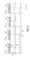
- FIG. 2illustrates operation of the system as a function of time “t”. Time is divided in successive time-frames (shown starting at times T 1 – 4 ). In each time frame a time interval 21 a–d occurs in which isochronous messages are transmitted, followed by a time interval 23 a–d in which other, non-isochronous messages are transmitted. The length of these time intervals 21 a–d , 23 a–d may vary from frame to frame, depending on the actual amount of data that has to be transferred. As shown, some of the time-frame may be left unused for transmission. This is not necessarily so; it also depends on the actual amount of data that needs to be transferred.
- FIG. 2shows, in addition, four lines representing, successively from top to bottom access to the first memory 122 a by the host controller 120 , access to the first memory 122 a by the processor 10 , access to the second memory 122 b by the host controller 120 , access to the second memory 122 b by the processor 10 .
- Right of accessis shown by a solid line, lack of that right is shown by dashed lines.
- host controller 120seizes access to alternate ones of the first and second memory 122 a,b , for the duration of the time interval 21 a–d for transfer of data from isochronous messages. That is, in the time intervals 21 a,c of the odd (first and third) time-frames (starting with T 1 , T 3 ) host controller 120 seizes access to the first memory 122 a and in the time intervals 21 b,d of the even (second and fourth) time frames (starting with T 2 , T 4 ) host controller 120 seizes control of the second memory 122 b .
- host controller 120writes or reads data to or from the memory 122 a,b to which it has seized control. This data is taken from received isochronous messages or put into transmitted isochronous messages.
- Processor 10has access to each of the first and second memory 122 a,b via internal bus 16 when host controller 120 has not seized control of the relevant memory 122 a,b .
- processor 10at least has access to each particular memory 122 a,b during the time-frame before the time frame in which host controller reads data from that memory 122 a,b for use in isochronous messages and in the time frame after the time-frame in which host controller 120 writes data from isochronous messages into that memory. This gives processor 10 the opportunity to write or read that data in one time frame and it gives host controller 120 the opportunity to receive and transmit isochronous messages without delay in another time frame.
- processor 10gets the opportunity in the remainder of the time frame to write or read that memory 122 a,b . Of course, this opportunity continues into the next time frame, since host controller 120 will read or write from the other memory 122 a,b in that time frame. In total therefore processor 10 gets an interval of more than a whole time-frame to read or write data for isochronous transmission.
- host controller 120seizes access to the first memory 122 a during the first time-frame in interval 20 from the start time T 1 of the time frame to the time I 1 at the end of isochronous message transfer. After that time I 1 host controller 120 relinquishes access in a time interval (shown as a dashed line 20 a ) until the start T 3 of the third time frame. From time I 1 to the start time T 3 of the third time-frame (interval of solid line 22 ) processor 10 has the opportunity to access the first memory 122 a .
- host controller 120seizes access to the second memory 122 b during the second time-frame in interval 24 from the start time T 2 of the time frame to the time I 2 at the end of isochronous message transfer. After that time I 2 host controller 120 relinquishes access in a time interval until the start T 4 of the fourth time frame. From time I 2 to the start time T 4 of the fourth time-frame (interval 26 ) processor 10 has the opportunity to access the second memory 122 a.
- non-isochronous messagesare transferred, using data from common memory 14 , until a time I 5 – 8 when no data is left or the time-frame ends.
- Host controller 120normally contends with processor 10 for access to the internal bus 16 to access common memory 14 . Therefore, if host controller 120 loses access to processor 10 , transfer of data for non-isochronous messages may have to be delayed.
- Host controller 120generates two interrupts for processor 10 per time frame, a first one at the time I 1 – 4 when isochronous message transfer has been completed and a second one at the time I 5 – 8 when non-isochronous transfer has been completed.
- the first interruptsignals that processor 10 gets back the opportunity to access that one of the first and second memory 122 a,b that the host controller 120 has used for isochronous data transfer in the current time frame. This enables the processor 10 to read or write data to that memory 122 a,b for the rest of that time frame and for the next time frame. Thus the processor 10 gets maximum opportunity to transfer data to or from the memory 122 a,b.
- the second interrupt(at time I 5 – 8 ) signals that host controller 120 has completed non-isochronous data transfer in the time frame. This enables processor 10 to adapt the data transfer to time intervals that lead to minimum interference with host controller 120 .
- FIG. 3shows the format of a transaction descriptor for USB message transfer.
- Processor 10loads data descriptors with this format into the memories 122 a,b , 14 to signal the need for message transfer to host controller 120 .
- the descriptoris followed by memory space for the data that is transferred. It will be noted that the descriptor is not necessarily limited to one message (also called “packet” in USB): the descriptor describes a block of data that host controller 120 may send or receive in one or more message.
- the meaning of the various fields in the descriptor and whether they are read or written by host controlleris illustrated in the following table.
- Host controller 120reads information from the descriptor, transmits or receives data according to the descriptor and writes back status information into the descriptor. Depending on whether a USB message is sent or received host controller 120 reads or writes the data following the descriptor.
- host controller 120visits the descriptors stored in memory 122 a,b sequentially during each frame and transmits or receives a message for each descriptor for which the “Active” bit is set. When all data for the descriptor has been transferred, host controller 120 clears the “Active” bit. When the host controller has transferred messages for all descriptors in a time frame and there is still time left, host controller 120 visits the descriptors again and transfers messages for those descriptors where the “Active” bit has not yet been cleared. Thus, a maximum amount of data can be transferred in a time-frame.
- data for one or more non-isochronous messagemay be stored in the first or second memory 122 a,b in addition to the data for the isochronous messages if there is room for this data.
- thismay limit transfer of this data to even or odd time frames if host controller 120 does not manage to transfer all data in one time frame.
- host controller 120may have an additional memory for buffering the data that is actually transferred, this data being fetched from memory 122 a,b , 14 or stored in the memory 122 a,b , 14 before or after completion of the message respectively.
- the processor 10may have a cache memory to store some of the data temporarily, the data from the cache being transferred when this is allowed by the host controller 120 .
- DMAmay be used to transfer data to and from the memories 122 a,b , 14 .
- special function registers in the processormay be used to access one or more of the memories.
Landscapes
- Engineering & Computer Science (AREA)
- Theoretical Computer Science (AREA)
- Physics & Mathematics (AREA)
- General Engineering & Computer Science (AREA)
- General Physics & Mathematics (AREA)
- Bus Control (AREA)
- Small-Scale Networks (AREA)
- Information Transfer Systems (AREA)
- Exchange Systems With Centralized Control (AREA)
Abstract
Description
| TABLE | ||||
| Name | Access | Description | ||
| ISO | R | indicates type of message | ||
| Speed | R | indicates speed of message | ||
| DirectionPID | R | direction of data flow: | ||
| in/out or setup (two-way) | ||||
| EndpointNumber | R | USB address of destination | ||
| endpoint within function | ||||
| FunctionAddress | R | USB address of destination | ||
| function | ||||
| Toggle | R/W | Toggled after each | ||
| successful transfer | ||||
| MaximumPacketSize | R | maximum number of bytes | ||
| per message | ||||
| TotalBytes | R | Total number of bytes | ||
| described by descriptor | ||||
| Active | R/W | Enable bit for host | ||
| controller/completion bit | ||||
| for processor | ||||
| Error | R/W | error indicator of transfer | ||
| ErrorCode | R/W | type of error | ||
| ActualBytes | R/W | number of bytes | ||
| transferred | ||||
Claims (5)
Applications Claiming Priority (3)
| Application Number | Priority Date | Filing Date | Title |
|---|---|---|---|
| EP012046645 | 2001-12-03 | ||
| EP01204664 | 2001-12-03 | ||
| PCT/IB2002/004866WO2003048950A1 (en) | 2001-12-03 | 2002-11-20 | Communication bus system |
Publications (2)
| Publication Number | Publication Date |
|---|---|
| US20050086411A1 US20050086411A1 (en) | 2005-04-21 |
| US7177997B2true US7177997B2 (en) | 2007-02-13 |
Family
ID=8181344
Family Applications (1)
| Application Number | Title | Priority Date | Filing Date |
|---|---|---|---|
| US10/497,048Expired - LifetimeUS7177997B2 (en) | 2001-12-03 | 2002-11-20 | Communication bus system |
Country Status (7)
| Country | Link |
|---|---|
| US (1) | US7177997B2 (en) |
| EP (1) | EP1459191B1 (en) |
| JP (1) | JP4477877B2 (en) |
| AT (1) | ATE496339T1 (en) |
| AU (1) | AU2002347472A1 (en) |
| DE (1) | DE60239011D1 (en) |
| WO (1) | WO2003048950A1 (en) |
Families Citing this family (1)
| Publication number | Priority date | Publication date | Assignee | Title |
|---|---|---|---|---|
| US7277988B2 (en) | 2004-10-29 | 2007-10-02 | International Business Machines Corporation | System, method and storage medium for providing data caching and data compression in a memory subsystem |
Citations (12)
| Publication number | Priority date | Publication date | Assignee | Title |
|---|---|---|---|---|
| US5361261A (en)* | 1992-11-02 | 1994-11-01 | National Semiconductor Corporation | Frame-based transmission of data |
| US5544324A (en)* | 1992-11-02 | 1996-08-06 | National Semiconductor Corporation | Network for transmitting isochronous-source data using a frame structure with variable number of time slots to compensate for timing variance between reference clock and data rate |
| US5559796A (en)* | 1995-02-28 | 1996-09-24 | National Semiconductor Corporation | Delay control for frame-based transmission of data |
| US5566169A (en)* | 1992-11-02 | 1996-10-15 | National Semiconductor Corporation | Data communication network with transfer port, cascade port and/or frame synchronizing signal |
| US5960001A (en)* | 1997-06-19 | 1999-09-28 | Siemens Information And Communication Networks, Inc. | Apparatus and method for guaranteeing isochronous data flow on a CSMA/CD network |
| US6101613A (en)* | 1998-07-06 | 2000-08-08 | Intel Corporation | Architecture providing isochronous access to memory in a system |
| US6339584B1 (en)* | 1996-04-12 | 2002-01-15 | Cirrus Logic, Inc. | Media access control for isochronous data packets in carrier sensing multiple access systems |
| US20020065966A1 (en)* | 1998-01-07 | 2002-05-30 | National Semiconductor Corporation | Apparatus and method of transmitting and receiving USB isochronous data |
| US20020174299A1 (en)* | 2001-05-18 | 2002-11-21 | Broadcom Corporation | Source controlled cache allocation |
| US6578109B1 (en)* | 2000-06-29 | 2003-06-10 | Sony Corporation | System and method for effectively implementing isochronous processor cache |
| US6658515B1 (en)* | 2000-01-25 | 2003-12-02 | Dell Usa, L.P. | Background execution of universal serial bus transactions |
| US6981073B2 (en)* | 2001-07-31 | 2005-12-27 | Wis Technologies, Inc. | Multiple channel data bus control for video processing |
Family Cites Families (2)
| Publication number | Priority date | Publication date | Assignee | Title |
|---|---|---|---|---|
| US5621898A (en)* | 1994-11-29 | 1997-04-15 | Compaq Computer Corporation | Arbiter organization for serial bus transfers |
| US6199132B1 (en)* | 1998-06-17 | 2001-03-06 | Advanced Micro Devices, Inc. | Communication link with isochronous and asynchronous priority modes |
- 2002
- 2002-11-20USUS10/497,048patent/US7177997B2/ennot_activeExpired - Lifetime
- 2002-11-20JPJP2003550075Apatent/JP4477877B2/ennot_activeExpired - Fee Related
- 2002-11-20AUAU2002347472Apatent/AU2002347472A1/ennot_activeAbandoned
- 2002-11-20DEDE60239011Tpatent/DE60239011D1/ennot_activeExpired - Lifetime
- 2002-11-20EPEP02783405Apatent/EP1459191B1/ennot_activeExpired - Lifetime
- 2002-11-20ATAT02783405Tpatent/ATE496339T1/ennot_activeIP Right Cessation
- 2002-11-20WOPCT/IB2002/004866patent/WO2003048950A1/enactiveApplication Filing
Patent Citations (13)
| Publication number | Priority date | Publication date | Assignee | Title |
|---|---|---|---|---|
| US5544324A (en)* | 1992-11-02 | 1996-08-06 | National Semiconductor Corporation | Network for transmitting isochronous-source data using a frame structure with variable number of time slots to compensate for timing variance between reference clock and data rate |
| US5566169A (en)* | 1992-11-02 | 1996-10-15 | National Semiconductor Corporation | Data communication network with transfer port, cascade port and/or frame synchronizing signal |
| US5594734A (en)* | 1992-11-02 | 1997-01-14 | National Semiconductor Corporation | Asynchronous processor access to a switch table in a network with isochronous capability |
| US5361261A (en)* | 1992-11-02 | 1994-11-01 | National Semiconductor Corporation | Frame-based transmission of data |
| US5559796A (en)* | 1995-02-28 | 1996-09-24 | National Semiconductor Corporation | Delay control for frame-based transmission of data |
| US6339584B1 (en)* | 1996-04-12 | 2002-01-15 | Cirrus Logic, Inc. | Media access control for isochronous data packets in carrier sensing multiple access systems |
| US5960001A (en)* | 1997-06-19 | 1999-09-28 | Siemens Information And Communication Networks, Inc. | Apparatus and method for guaranteeing isochronous data flow on a CSMA/CD network |
| US20020065966A1 (en)* | 1998-01-07 | 2002-05-30 | National Semiconductor Corporation | Apparatus and method of transmitting and receiving USB isochronous data |
| US6101613A (en)* | 1998-07-06 | 2000-08-08 | Intel Corporation | Architecture providing isochronous access to memory in a system |
| US6658515B1 (en)* | 2000-01-25 | 2003-12-02 | Dell Usa, L.P. | Background execution of universal serial bus transactions |
| US6578109B1 (en)* | 2000-06-29 | 2003-06-10 | Sony Corporation | System and method for effectively implementing isochronous processor cache |
| US20020174299A1 (en)* | 2001-05-18 | 2002-11-21 | Broadcom Corporation | Source controlled cache allocation |
| US6981073B2 (en)* | 2001-07-31 | 2005-12-27 | Wis Technologies, Inc. | Multiple channel data bus control for video processing |
Also Published As
| Publication number | Publication date |
|---|---|
| EP1459191B1 (en) | 2011-01-19 |
| JP2005512193A (en) | 2005-04-28 |
| DE60239011D1 (en) | 2011-03-03 |
| JP4477877B2 (en) | 2010-06-09 |
| EP1459191A1 (en) | 2004-09-22 |
| US20050086411A1 (en) | 2005-04-21 |
| AU2002347472A1 (en) | 2003-06-17 |
| WO2003048950A1 (en) | 2003-06-12 |
| ATE496339T1 (en) | 2011-02-15 |
Similar Documents
| Publication | Publication Date | Title |
|---|---|---|
| US5261059A (en) | Crossbar interface for data communication network | |
| US5546543A (en) | Method for assigning priority to receive and transmit requests in response to occupancy of receive and transmit buffers when transmission and reception are in progress | |
| US6035360A (en) | Multi-port SRAM access control using time division multiplexed arbitration | |
| US6119196A (en) | System having multiple arbitrating levels for arbitrating access to a shared memory by network ports operating at different data rates | |
| US5958031A (en) | Data transmitting/receiving device of a multiprocessor system and method therefor | |
| EP0993680B1 (en) | Method and apparatus in a packet routing switch for controlling access at different data rates to a shared memory | |
| KR100814904B1 (en) | On-Chip Communication architecture | |
| JP2002009849A (en) | Usb transfer control method and usb controller | |
| JPH10507023A (en) | Shared memory system | |
| JPH09251437A (en) | Computer device and continuous data server device | |
| EP1288785B1 (en) | Method and interface for improved efficiency in performing bus-to-bus read data transfers | |
| US6131114A (en) | System for interchanging data between data processor units having processors interconnected by a common bus | |
| JP2008541276A (en) | Simultaneous read response confirmation extended direct memory access unit | |
| US4796022A (en) | Double transit bus system | |
| EP0821311B1 (en) | Data processing and communicating system with high throughput peripheral component interconnect bus | |
| JP4104939B2 (en) | Multiprocessor system | |
| US7177997B2 (en) | Communication bus system | |
| WO2001050216A2 (en) | Communication bus for a multi-processor system | |
| US7711787B2 (en) | On-chip network interfacing apparatus and method | |
| JPH07271654A (en) | Controller | |
| CN118733498B (en) | Memory controller | |
| JP4125933B2 (en) | Processor system with common memory | |
| JPH04282938A (en) | Communication control device | |
| JP3233470B2 (en) | Computer system | |
| JP2004054419A (en) | Inter-node transaction processor |
Legal Events
| Date | Code | Title | Description |
|---|---|---|---|
| AS | Assignment | Owner name:KONNINKLIJKE PHILIPS ELECTRONICS N.V., NETHERLANDS Free format text:ASSIGNMENT OF ASSIGNORS INTEREST;ASSIGNOR:WU, ZONG LIANG;REEL/FRAME:015822/0499 Effective date:20030220 | |
| STCF | Information on status: patent grant | Free format text:PATENTED CASE | |
| AS | Assignment | Owner name:NXP B.V., NETHERLANDS Free format text:ASSIGNMENT OF ASSIGNORS INTEREST;ASSIGNOR:KONINKLIJKE PHILIPS ELECTRONICS N.V.;REEL/FRAME:019719/0843 Effective date:20070704 Owner name:NXP B.V.,NETHERLANDS Free format text:ASSIGNMENT OF ASSIGNORS INTEREST;ASSIGNOR:KONINKLIJKE PHILIPS ELECTRONICS N.V.;REEL/FRAME:019719/0843 Effective date:20070704 | |
| FEPP | Fee payment procedure | Free format text:PAYER NUMBER DE-ASSIGNED (ORIGINAL EVENT CODE: RMPN); ENTITY STATUS OF PATENT OWNER: LARGE ENTITY Free format text:PAYOR NUMBER ASSIGNED (ORIGINAL EVENT CODE: ASPN); ENTITY STATUS OF PATENT OWNER: LARGE ENTITY | |
| FPAY | Fee payment | Year of fee payment:4 | |
| FPAY | Fee payment | Year of fee payment:8 | |
| AS | Assignment | Owner name:ST WIRELESS SA, SWITZERLAND Free format text:ASSIGNMENT OF ASSIGNORS INTEREST;ASSIGNOR:NXP B.V.;REEL/FRAME:037624/0831 Effective date:20080728 | |
| AS | Assignment | Owner name:ST-ERICSSON SA, SWITZERLAND Free format text:CHANGE OF NAME;ASSIGNOR:ST WIRELESS SA;REEL/FRAME:037683/0128 Effective date:20080714 Owner name:ST-ERICSSON SA, EN LIQUIDATION, SWITZERLAND Free format text:STATUS CHANGE-ENTITY IN LIQUIDATION;ASSIGNOR:ST-ERICSSON SA;REEL/FRAME:037739/0493 Effective date:20150223 | |
| MAFP | Maintenance fee payment | Free format text:PAYMENT OF MAINTENANCE FEE, 12TH YEAR, LARGE ENTITY (ORIGINAL EVENT CODE: M1553) Year of fee payment:12 |