US7177200B2 - Two-phase programming of a flash memory - Google Patents
Two-phase programming of a flash memoryDownload PDFInfo
- Publication number
- US7177200B2 US7177200B2US10/902,866US90286604AUS7177200B2US 7177200 B2US7177200 B2US 7177200B2US 90286604 AUS90286604 AUS 90286604AUS 7177200 B2US7177200 B2US 7177200B2
- Authority
- US
- United States
- Prior art keywords
- cell
- voltage
- reference voltage
- state
- indicative
- Prior art date
- Legal status (The legal status is an assumption and is not a legal conclusion. Google has not performed a legal analysis and makes no representation as to the accuracy of the status listed.)
- Expired - Lifetime, expires
Links
- 230000015654memoryEffects0.000titleclaimsabstractdescription47
- 238000000034methodMethods0.000claimsdescription41
- 230000014759maintenance of locationEffects0.000claimsdescription9
- 238000009826distributionMethods0.000description18
- 238000004242micellar liquid chromatographyMethods0.000description11
- 238000010586diagramMethods0.000description3
- 230000007774longtermEffects0.000description3
- 230000008901benefitEffects0.000description2
- 238000005516engineering processMethods0.000description2
- XUIMIQQOPSSXEZ-UHFFFAOYSA-NSiliconChemical compound[Si]XUIMIQQOPSSXEZ-UHFFFAOYSA-N0.000description1
- 238000002347injectionMethods0.000description1
- 239000007924injectionSubstances0.000description1
- 238000012986modificationMethods0.000description1
- 230000004048modificationEffects0.000description1
- 230000000704physical effectEffects0.000description1
- 229910052710siliconInorganic materials0.000description1
- 239000010703siliconSubstances0.000description1
- 239000000758substrateSubstances0.000description1
- 230000005641tunnelingEffects0.000description1
Images

Classifications
- G—PHYSICS
- G11—INFORMATION STORAGE
- G11C—STATIC STORES
- G11C16/00—Erasable programmable read-only memories
- G11C16/02—Erasable programmable read-only memories electrically programmable
- G11C16/06—Auxiliary circuits, e.g. for writing into memory
- G11C16/10—Programming or data input circuits
- G—PHYSICS
- G11—INFORMATION STORAGE
- G11C—STATIC STORES
- G11C16/00—Erasable programmable read-only memories
- G11C16/02—Erasable programmable read-only memories electrically programmable
- G11C16/06—Auxiliary circuits, e.g. for writing into memory
- G11C16/10—Programming or data input circuits
- G11C16/12—Programming voltage switching circuits
- G—PHYSICS
- G11—INFORMATION STORAGE
- G11C—STATIC STORES
- G11C16/00—Erasable programmable read-only memories
- G11C16/02—Erasable programmable read-only memories electrically programmable
- G11C16/04—Erasable programmable read-only memories electrically programmable using variable threshold transistors, e.g. FAMOS
- G—PHYSICS
- G11—INFORMATION STORAGE
- G11C—STATIC STORES
- G11C16/00—Erasable programmable read-only memories
- G11C16/02—Erasable programmable read-only memories electrically programmable
- G11C16/06—Auxiliary circuits, e.g. for writing into memory
- G11C16/34—Determination of programming status, e.g. threshold voltage, overprogramming or underprogramming, retention
- G11C16/3436—Arrangements for verifying correct programming or erasure
- G11C16/3468—Prevention of overerasure or overprogramming, e.g. by verifying whilst erasing or writing
Definitions
- the present inventionrelates to flash memories and, more particularly, to a method of increasing the effective programming speed of a flash memory with no loss in reliability.
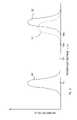
- FIG. 1illustrates the storage of a bit, either a zero bit or a one bit, in a cell of an electrically programmable memory (EPROM) such as a flash memory.
- EPROMelectrically programmable memory
- the cell that is the subject of FIG. 1is a single-level cell (SLC).
- SLCsingle-level cell
- the cellhas a nominal threshold voltage V 1 that represents a one bit.
- V 1represents a one bit.
- the actual threshold voltagesare distributed around the nominal threshold voltage V 1 according to a distribution curve 10 .
- a train of programming voltage pulsesis applied, in order to inject electrons from the cell's silicon substrate through the cell's oxide layer into the cell's floating gate, until the cell's threshold voltage exceeds a reference voltage V 0 that represents a zero bit. Because the electrons move through the oxide layer by quantum mechanical tunneling or by hot injection, because of non-uniformities in the cells' structures, and because the initial threshold voltages are distributed according to distribution curve 10 , the threshold voltages of the cells that store zero bits are distributed above V 0 according to a distribution curve 12 .
- a cellis read by comparing the cell's threshold voltage to a reference voltage V R that is above distribution curve 10 but below V 0 . If the cell's threshold voltage is below V R then the cell's contents are read as a one bit. If the cell's threshold voltage is at or above V R then the cell's contents are read as a zero bit.
- a distribution curve 14that represents the distribution of the threshold voltages of the cells that have been programmed to store zero bits after the passage of a considerable amount of time.
- V 1 , V R and V 0are selected to be sufficiently far apart to preserve the reliability of the flash memory despite this drift of the threshold voltages.
- the voltage difference between the successive voltage pulses that are used to program a cellare relatively small, for two reasons.
- a SLCand in the case of the highest voltage band of a multi-level cell (MLC, in which each of 2 n voltage bands corresponds to one of the 2 n possible patterns of n bits), too high a programming voltage imposes stress on the cell that reduces the cell's useful lifetime.
- distribution 12In the case of the intermediate voltage bands of an MLC, distribution 12 must be sufficiently narrow to fit within the voltage band that represents the corresponding bit pattern.
- the use of small voltage incrementsimplies that the programming of an array of flash cells is a relatively slow process. There is thus a widely recognized need for, and it would be highly advantageous to have, a method of programming flash memory cells that is faster than the presently known methods, with no loss in reliability.
- a method of storing a datum in a memoryincluding the steps of: (a) placing a cell of the memory in a first state that is indicative of the datum; and (b) placing the cell in a second state that is indicative of the datum, the second state having a longer data retention time than the first state.
- a memory deviceincluding: (a) at least one cell; and (b) a controller operative: (i) to place one of the at least one cell in a first state that is indicative of a datum, and (ii) to place the one cell in a second state that is indicative of the datum, the second state having a longer data retention time than the first state.
- a method of storing a datum in a memorythat includes a plurality of cells, the method including the steps of: (a) placing a first cell of the memory in a first state that is indicative of the datum; and (b) placing a second cell of the memory in a second state that is indicative of the datum, the second state having a longer data retention time than the first state; wherein the first cell and the second cell store an identical number of bits.
- a memory deviceincluding: (a) an array of cells; and (b) a controller operative: (i) to place a first of the cells in a first state that is indicative of a datum, and (ii) to place a second of the cells in a second state that is indicative of the datum, the second state having a longer data retention time than the first state wherein the first cell and the second cell store an identical number of bits.
- a method of operating a memorythat includes a plurality of cells, including the steps of: (a) for each of at least one of the cells: (i) comparing a threshold voltage of the each cell to a first reference voltage that is indicative of a certain bit pattern, and (ii) comparing the threshold voltage of the each cell to a second reference voltage that is greater than the first reference voltage and that also is indicative of the bit pattern; and (b) for each at least one cell, if the comparing shows that the threshold voltage of the each cell is between the first reference voltage and the second reference voltage: applying at least one voltage pulse to the each cell until the threshold voltage of the each cell is greater than the second reference voltage.
- a memory deviceincluding: (a) at least one cell; and (b) a controller operative, for each at least one cell for which a comparison of a threshold voltage of the each cell to a first reference voltage that is indicative of a certain bit pattern and to a second reference voltage that is indicative of said bit pattern shows that the threshold voltage of the each cell is between the first reference voltage and the second reference voltage: to apply at least one voltage pulse to the each cell until the threshold voltage of the each cell is greater than the second reference voltage.
- a method of operating a memorythat includes a plurality of cells, including the steps of: (a) for each of at least one of the cells: (i) comparing a threshold voltage of the each cell to a first reference voltage that is indicative of a certain bit pattern, and (ii) comparing the threshold voltage of the each cell to a second reference voltage that is greater than the first reference voltage and that also is indicative of the bit pattern; and (b) for each at least one cell, if the comparing shows that the threshold voltage of the each cell is between the first reference voltage and the second reference voltage: applying at least one voltage pulse to a corresponding other cell until a threshold voltage of the corresponding other cell is greater than the second reference voltage.
- a memory deviceincluding: (a) an array of cells; and (b) a controller operative, for each cell of the array for which a comparison of a threshold voltage of the each cell to a first reference voltage that is indicative of a certain bit pattern and to a second reference voltage that is indicative of said bit pattern shows that the threshold voltage of the each cell is between the first reference voltage and the second reference voltage: to apply at least one voltage pulse to a corresponding other cell of the array until a threshold voltage of the corresponding other cell is greater than the second reference voltage.
- the present inventionis a method of storing data in a memory such as a flash memory.
- a memorysuch as a flash memory.
- the description hereinis directed at flash memories, the scope of the present invention includes any memory, such as an EPROM, that is programmed by placing cells of the memory in respective states that are indicative of the data stored therein, for example by using trains of programming voltage pulses.
- each cell of the memoryis stored a “datum”.
- a “datum”is a string of one or more bits that is stored in the cell by a host. How many bits are stored per cell depends on how the memory is configured.
- SLC cellsstore one bit per cell.
- MLCsstore more than one bit per cell.
- a SLC in its unprogrammed stateconventionally is interpreted as storing a one bit.
- a MLC in its unprogrammed stateconventionally is interpreted as storing a string of one bits.
- the methods of the present inventionare methods of programming memory cells to store data that are not one bits (SLCs) or strings of one bits (MLCs).
- a memory cellis programmed to store a datum by placing the cell in a first state that is indicative of the datum. Then the cell is placed in a second state that also is indicative of the datum. That a cell is in a state that is “indicative” of a datum means that, according to a test of a physical property of the cell, such as the cell's threshold voltage, the cell is interpreted as storing that datum.
- the datumis a logical datum that is received from a host and has a specific meaning to the host. Both the first state and the second state indicate the same information with the same meaning to the host.
- the scope of the present inventionspecifically excludes, for example, programming a SLC to store a zero bit from one of the host's data sets, erasing the SLC, and then again programming the SLC to store a zero bit from another one of the host's data sets.
- the cellis placed in the first state by steps including applying a first train of one or more programming voltage pulses to the cell until the cell's threshold voltage exceeds a first reference voltage.
- the cellis placed in the second state by steps including applying a second train of one or more programming voltage pulses until the cell's threshold voltage exceeds a second, different reference voltage.
- the second reference voltageis greater than the first reference voltage.
- the first train of programming voltage pulsesincludes a monotonically increasing plurality of the voltage pulses
- the second train of programming voltage pulsesalso includes a monotonically increasing plurality of the voltage pulses.
- successive voltage pulses of the first traindiffer by a first common increment (voltage step size)
- successive voltage pulses of the second traindiffer by a second common increment that is less than the first common increment.
- a first memory cellis programmed to store a datum by placing the first cell in a first state that is indicative of the datum. Then a second, different memory cell is programmed to store the same datum by placing the second cell in a second state that is indicative of the datum. Both cells are programmed to store the same number of bits.
- the latter limitationdistinguishes the present invention from Lee et al., U.S. Pat. No. 5,930,167, who initially store data in SLCs and then compress the same data into MLCs.
- the first cellthen is erased.
- the first cellis placed in the first state by applying a first train of one or more programming voltage pulses to the first cell until the first cell's threshold voltage exceeds a first reference voltage.
- the second cellis placed in the second state by applying a train of one or more programming voltage pulses to the second cell until the threshold voltage of the second cell exceeds a second, different reference voltage.
- the second reference voltageis greater than the first reference voltage.
- the first train of programming voltage pulsesincludes a monotonically increasing plurality of the voltage pulses
- the second train of programming voltage pulsesalso includes a monotonically increasing plurality of the voltage pulses.
- successive voltage pulses of the first traindiffer by a first common increment (voltage step size)
- successive voltage pulses of the second traindiffer by a second common increment that is less than the first common increment.
- a third basic method of the present inventionis useful in recovering from interruptions of the first two methods by losses of power, and also is useful for reversing the drift over time of threshold voltages that is illustrated in FIG. 1 .
- This methodis a method of operating a memory that includes a plurality of memory cells. According to this method, the threshold voltages of one or more of the cells are compared to a first reference voltage and to a second, greater reference voltage, both reference voltages being indicative of the same bit pattern. (That a reference voltage is “indicative” of a bit pattern means that the reference voltage is the lower bound of a voltage band such that if the cell's threshold voltage is within that voltage band then the cell is interpreted as storing that bit pattern.
- the reference voltages V R and V 0 of FIG. 1are indicative of the bit pattern “0”, because if a comparison of the threshold voltage of the cell to V R or to V 0 shows that the threshold voltage of the cell exceeds that reference voltage then the cell is interpreted as storing a zero bit.
- the reference voltages of a four-level MLCcould be indicative of the bit patterns “10”, “01” or “00”.)
- a train of at least one programming voltage pulseis applied either to the same cell or to a corresponding other cell (typically an unprogrammed or freshly erased cell) until the threshold voltage of the cell to which the train of programming voltage(s) is applied exceeds the second reference voltage. If the train of programming voltage(s) is applied to a corresponding other cell, then preferably the cell whose threshold voltage was found to be between the two reference voltages is erased.
- the scope of the present inventionalso includes memory devices that operate according to the methods of the present invention.
- FIG. 1illustrates the storage of a datum bit in an EPROM cell according to the prior art
- FIG. 2illustrates the storage of a datum bit in an EPROM cell according to the present invention
- FIGS. 3 and 4are high-level block diagrams of memory devices of the present invention.
- the present inventionis of a method of programming a memory such as a flash memory, at an effective speed greater than that of prior art methods, with no loss in reliability.
- the present inventiontakes advantage of the fact that a host of a memory device such as a flash memory device typically exchanges data with the memory device only intermittently.
- a host of a memory devicesuch as a flash memory device typically exchanges data with the memory device only intermittently.
- the user of the camerararely if ever takes pictures at such a fast rate that the camera is continuously engaged in writing acquired digital images to the flash memory device.
- a photographersometimes desires to take a small number of pictures in quick succession, with the delay between successive pictures being as short as possible. This mandates that the flash cells that store the pictures be programmed as fast as possible.
- the basic idea of the present inventionis to program the flash memory of the flash memory device in a quick and dirty manner that produces relatively broad threshold voltage distributions that would render the flash memory unreliable in the long term if left uncorrected. Then, while the host of the flash memory device is idle, the flash memory device shifts and tightens up its threshold voltage distributions sufficiently to obtain long-term reliability.
- FIG. 2is FIG. 1 modified according to the principles of the present invention.
- FIG. 2is identical to FIG. 1 , but with reference voltage V 0 relabeled as “V 0B ” and with a new reference voltage, V 0A , introduced at the left end of distribution 14 .
- a SLC flash memory device of the present inventionhas two programming modes.
- the first modeis identical to the prior art mode.
- the second modeis a fast programming mode in which a first train of programming voltage pulses is applied to each cell that is to store a zero bit only until the cell's threshold voltage exceeds V 0A .
- the cells that need to be programmedare programmed faster than in the prior art, under which the first train of programming voltage pulses would be applied to each cell that is to store a zero bit until the cell's threshold voltage exceeds V 0B . Note that because V 0A >V R , every cell whose threshold voltage exceeds V 0A is read correctly as storing a zero bit.
- the on-board controller of the flash memory devicereads the cells that were programmed in fast programming mode. For every cell that stores a zero bit (according to the comparison to V R ), the cell's threshold voltage is compared to V 0B . If the cell's threshold voltage is below V 0B , then a second train of programming voltage pulses is applied to the cell to raise the cell's threshold voltage above V 0B .
- the voltage step size of the second train of programming voltage pulsesis the same as the prior art step size.
- the voltage step size of the first train of programming voltage pulsesis made greater than the prior art step size. This results in a wider distribution of programmed threshold voltages than according to the prior art. For example, as illustrated in FIG. 2 , the resulting distribution of threshold voltages could resemble distribution 14 that results from the downward drift over time of prior art distribution 12 . This unnecessarily wide distribution is tightened in the second phase of the fast programming mode, in which the second trains of programming voltage pulses are applied to cells as needed to raise the cells' threshold voltages above V 0B . The resulting threshold voltage distribution resembles distribution 12 , as illustrated in FIG. 2 .
- Some flash technologieshave restrictions, for example restrictions on partial page programming or restrictions on non-sequential page writing, that prevent the application of the second trains of programming voltage pulses to cells that have been programmed using the first trains of programming voltage pulses.
- the cells that were programmed using the first trains of programming voltage pulsesare copied to fresh (never-programmed or newly erased) flash cells using the prior art method and so inherently producing threshold voltage distribution 12 .
- this copying operationstores as many bits per new cell (one bit per cell in the present example) as were stored in the cells that are being copied.
- this aspect of the present inventiondistinguishes the present invention from the teachings of U.S. Pat. No. 5,930,167.
- a flash memory device of the present inventionmay experience a loss of power between the first and second phases of the fast programming mode. Therefore, on power-up, the flash memory device always enters the second phase of the fast programming mode, to make sure that any cell whose threshold voltages should have been raised above V 0B is in fact raised above V 0B .
- This method of power-uphas the additional benefit that threshold voltages that were programmed correctly to be above V 0B but that meanwhile have drifted below V 0B are raised back up above V 0B . Long-term downward drift of threshold voltages thus is eliminated as a limit on the useful data retention time of a flash memory device.
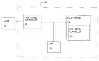
- FIG. 3is a high-level block diagram of a memory device 20 of the present invention, coupled to a host 30 .
- FIG. 3is adapted from FIG. 1 of Ban, U.S. Pat. No. 5,404,485, which patent is incorporated by reference for all purposes as if fully set forth herein.
- Memory device 20includes a flash memory 24 , a high-level controller 22 and a random access memory (RAM) 26 .
- High-level controller 22that corresponds to “flash control 14 ” of U.S. Pat. No. 5,404,485, manages flash memory 24 , with the help of RAM 26 , as described in U.S. Pat. No. 5,404,485.
- Flash memory 24includes a low-level controller 28 that translates the commands received from high-level controller 22 into hardware-level commands. For example, low-level controller 28 translates the command to program a cell into a train of voltage pulses, selects the threshold voltage, etc. Low-level controller 28 supports two different kinds of programming commands, corresponding to the two programming modes of the present invention, a slow (prior art) programming mode and a fast programming mode, as described above.
- the “controller” that is recited in the appended claimsis such a low-level controller.
- FIG. 4is a high-level block diagram of another memory device 40 of the present invention, coupled to a host 50 .
- memory device 40includes, from among the components of flash memory 20 that are illustrated in FIG. 3 , only flash memory 24 with low-level controller 28 .
- Processor 52 of host 50emulates controller 22 by executing a software driver, such as the TrueFFSTM driver of M-Systems Flash Disk Pioneers Ltd. of Kfar Saba, Israel, that implements the methodology of U.S. Pat. No. 5,404,485.
- a software driversuch as the TrueFFSTM driver of M-Systems Flash Disk Pioneers Ltd. of Kfar Saba, Israel, that implements the methodology of U.S. Pat. No. 5,404,485.
Landscapes
- Engineering & Computer Science (AREA)
- Microelectronics & Electronic Packaging (AREA)
- Read Only Memory (AREA)
Abstract
Description
Claims (18)
Priority Applications (3)
| Application Number | Priority Date | Filing Date | Title |
|---|---|---|---|
| US10/902,866US7177200B2 (en) | 2004-02-10 | 2004-08-02 | Two-phase programming of a flash memory |
| PCT/IL2005/000031WO2005074386A2 (en) | 2004-02-10 | 2005-01-09 | Two-phase programming of a flash memory |
| KR1020067017507AKR100897010B1 (en) | 2004-02-10 | 2005-01-09 | Two-phase programming of a flash memory |
Applications Claiming Priority (2)
| Application Number | Priority Date | Filing Date | Title |
|---|---|---|---|
| US54427304P | 2004-02-10 | 2004-02-10 | |
| US10/902,866US7177200B2 (en) | 2004-02-10 | 2004-08-02 | Two-phase programming of a flash memory |
Related Parent Applications (1)
| Application Number | Title | Priority Date | Filing Date |
|---|---|---|---|
| US54427304PContinuation-In-Part | 2004-02-10 | 2004-02-10 |
Publications (2)
| Publication Number | Publication Date |
|---|---|
| US20050174853A1 US20050174853A1 (en) | 2005-08-11 |
| US7177200B2true US7177200B2 (en) | 2007-02-13 |
Family
ID=34841166
Family Applications (1)
| Application Number | Title | Priority Date | Filing Date |
|---|---|---|---|
| US10/902,866Expired - LifetimeUS7177200B2 (en) | 2004-02-10 | 2004-08-02 | Two-phase programming of a flash memory |
Country Status (3)
| Country | Link |
|---|---|
| US (1) | US7177200B2 (en) |
| KR (1) | KR100897010B1 (en) |
| WO (1) | WO2005074386A2 (en) |
Cited By (70)
| Publication number | Priority date | Publication date | Assignee | Title |
|---|---|---|---|---|
| US20060064575A1 (en)* | 2004-09-23 | 2006-03-23 | Jo Seong-Kue | Multi chip system and its boot code fetch method |
| US20080082751A1 (en)* | 2006-09-28 | 2008-04-03 | Okin Kenneth A | Memory modules and programmable heterogeneous memory controllers for main memory |
| US20080148115A1 (en)* | 2006-12-17 | 2008-06-19 | Anobit Technologies Ltd. | High-speed programming of memory devices |
| US20080158958A1 (en)* | 2006-12-17 | 2008-07-03 | Anobit Technologies Ltd. | Memory device with reduced reading |
| US20080219050A1 (en)* | 2007-01-24 | 2008-09-11 | Anobit Technologies Ltd. | Reduction of back pattern dependency effects in memory devices |
| US20080263262A1 (en)* | 2007-04-22 | 2008-10-23 | Anobit Technologies Ltd. | Command interface for memory devices |
| US20080282106A1 (en)* | 2007-05-12 | 2008-11-13 | Anobit Technologies Ltd | Data storage with incremental redundancy |
| US20090024905A1 (en)* | 2006-05-12 | 2009-01-22 | Anobit Technologies Ltd. | Combined distortion estimation and error correction coding for memory devices |
| US20090106485A1 (en)* | 2007-10-19 | 2009-04-23 | Anobit Technologies Ltd. | Reading analog memory cells using built-in multi-threshold commands |
| US20090158126A1 (en)* | 2007-12-12 | 2009-06-18 | Anobit Technologies Ltd | Efficient interference cancellation in analog memory cell arrays |
| US20090168524A1 (en)* | 2007-12-27 | 2009-07-02 | Anobit Technologies Ltd. | Wear level estimation in analog memory cells |
| US20090199074A1 (en)* | 2008-02-05 | 2009-08-06 | Anobit Technologies Ltd. | Parameter estimation based on error correction code parity check equations |
| US20090213653A1 (en)* | 2008-02-21 | 2009-08-27 | Anobit Technologies Ltd | Programming of analog memory cells using a single programming pulse per state transition |
| US20090228761A1 (en)* | 2008-03-07 | 2009-09-10 | Anobit Technologies Ltd | Efficient readout from analog memory cells using data compression |
| US20090240872A1 (en)* | 2008-03-18 | 2009-09-24 | Anobit Technologies Ltd | Memory device with multiple-accuracy read commands |
| US7697326B2 (en) | 2006-05-12 | 2010-04-13 | Anobit Technologies Ltd. | Reducing programming error in memory devices |
| US20100091535A1 (en)* | 2007-03-12 | 2010-04-15 | Anobit Technologies Ltd | Adaptive estimation of memory cell read thresholds |
| US20100115376A1 (en)* | 2006-12-03 | 2010-05-06 | Anobit Technologies Ltd. | Automatic defect management in memory devices |
| US20100157675A1 (en)* | 2007-09-19 | 2010-06-24 | Anobit Technologies Ltd | Programming orders for reducing distortion in arrays of multi-level analog memory cells |
| US20100157641A1 (en)* | 2006-05-12 | 2010-06-24 | Anobit Technologies Ltd. | Memory device with adaptive capacity |
| US20100165689A1 (en)* | 2008-12-31 | 2010-07-01 | Anobit Technologies Ltd | Rejuvenation of analog memory cells |
| US7751240B2 (en) | 2007-01-24 | 2010-07-06 | Anobit Technologies Ltd. | Memory device with negative thresholds |
| US20100199150A1 (en)* | 2007-10-19 | 2010-08-05 | Anobit Technologies Ltd | Data Storage In Analog Memory Cell Arrays Having Erase Failures |
| US7773413B2 (en) | 2007-10-08 | 2010-08-10 | Anobit Technologies Ltd. | Reliable data storage in analog memory cells in the presence of temperature variations |
| US20100220510A1 (en)* | 2007-11-13 | 2010-09-02 | Anobit Technologies Ltd | Optimized Selection of Memory Chips in Multi-Chips Memory Devices |
| US20100250836A1 (en)* | 2009-03-25 | 2010-09-30 | Anobit Technologies Ltd | Use of Host System Resources by Memory Controller |
| US7821826B2 (en) | 2006-10-30 | 2010-10-26 | Anobit Technologies, Ltd. | Memory cell readout using successive approximation |
| US7864573B2 (en) | 2008-02-24 | 2011-01-04 | Anobit Technologies Ltd. | Programming analog memory cells for reduced variance after retention |
| US7924648B2 (en) | 2006-11-28 | 2011-04-12 | Anobit Technologies Ltd. | Memory power and performance management |
| US7925936B1 (en) | 2007-07-13 | 2011-04-12 | Anobit Technologies Ltd. | Memory device with non-uniform programming levels |
| US7924613B1 (en) | 2008-08-05 | 2011-04-12 | Anobit Technologies Ltd. | Data storage in analog memory cells with protection against programming interruption |
| US7975192B2 (en) | 2006-10-30 | 2011-07-05 | Anobit Technologies Ltd. | Reading memory cells using multiple thresholds |
| US7995388B1 (en) | 2008-08-05 | 2011-08-09 | Anobit Technologies Ltd. | Data storage using modified voltages |
| US8000135B1 (en) | 2008-09-14 | 2011-08-16 | Anobit Technologies Ltd. | Estimation of memory cell read thresholds by sampling inside programming level distribution intervals |
| US8000141B1 (en) | 2007-10-19 | 2011-08-16 | Anobit Technologies Ltd. | Compensation for voltage drifts in analog memory cells |
| US8050086B2 (en) | 2006-05-12 | 2011-11-01 | Anobit Technologies Ltd. | Distortion estimation and cancellation in memory devices |
| US8060806B2 (en) | 2006-08-27 | 2011-11-15 | Anobit Technologies Ltd. | Estimation of non-linear distortion in memory devices |
| US8169825B1 (en) | 2008-09-02 | 2012-05-01 | Anobit Technologies Ltd. | Reliable data storage in analog memory cells subjected to long retention periods |
| US8174857B1 (en) | 2008-12-31 | 2012-05-08 | Anobit Technologies Ltd. | Efficient readout schemes for analog memory cell devices using multiple read threshold sets |
| US8208304B2 (en) | 2008-11-16 | 2012-06-26 | Anobit Technologies Ltd. | Storage at M bits/cell density in N bits/cell analog memory cell devices, M>N |
| US8225181B2 (en) | 2007-11-30 | 2012-07-17 | Apple Inc. | Efficient re-read operations from memory devices |
| US8228701B2 (en) | 2009-03-01 | 2012-07-24 | Apple Inc. | Selective activation of programming schemes in analog memory cell arrays |
| US8238157B1 (en) | 2009-04-12 | 2012-08-07 | Apple Inc. | Selective re-programming of analog memory cells |
| US8239734B1 (en) | 2008-10-15 | 2012-08-07 | Apple Inc. | Efficient data storage in storage device arrays |
| US8259506B1 (en) | 2009-03-25 | 2012-09-04 | Apple Inc. | Database of memory read thresholds |
| US8259497B2 (en) | 2007-08-06 | 2012-09-04 | Apple Inc. | Programming schemes for multi-level analog memory cells |
| US8261159B1 (en) | 2008-10-30 | 2012-09-04 | Apple, Inc. | Data scrambling schemes for memory devices |
| US8400858B2 (en) | 2008-03-18 | 2013-03-19 | Apple Inc. | Memory device with reduced sense time readout |
| US8429493B2 (en) | 2007-05-12 | 2013-04-23 | Apple Inc. | Memory device with internal signap processing unit |
| US8456905B2 (en) | 2007-12-16 | 2013-06-04 | Apple Inc. | Efficient data storage in multi-plane memory devices |
| US8479080B1 (en) | 2009-07-12 | 2013-07-02 | Apple Inc. | Adaptive over-provisioning in memory systems |
| US8482978B1 (en) | 2008-09-14 | 2013-07-09 | Apple Inc. | Estimation of memory cell read thresholds by sampling inside programming level distribution intervals |
| US8495465B1 (en) | 2009-10-15 | 2013-07-23 | Apple Inc. | Error correction coding over multiple memory pages |
| US8572311B1 (en) | 2010-01-11 | 2013-10-29 | Apple Inc. | Redundant data storage in multi-die memory systems |
| US8572423B1 (en) | 2010-06-22 | 2013-10-29 | Apple Inc. | Reducing peak current in memory systems |
| US8595591B1 (en) | 2010-07-11 | 2013-11-26 | Apple Inc. | Interference-aware assignment of programming levels in analog memory cells |
| US8645794B1 (en) | 2010-07-31 | 2014-02-04 | Apple Inc. | Data storage in analog memory cells using a non-integer number of bits per cell |
| US8677054B1 (en) | 2009-12-16 | 2014-03-18 | Apple Inc. | Memory management schemes for non-volatile memory devices |
| US8694854B1 (en) | 2010-08-17 | 2014-04-08 | Apple Inc. | Read threshold setting based on soft readout statistics |
| US8694814B1 (en) | 2010-01-10 | 2014-04-08 | Apple Inc. | Reuse of host hibernation storage space by memory controller |
| US8694853B1 (en) | 2010-05-04 | 2014-04-08 | Apple Inc. | Read commands for reading interfering memory cells |
| US8856475B1 (en) | 2010-08-01 | 2014-10-07 | Apple Inc. | Efficient selection of memory blocks for compaction |
| US8924661B1 (en) | 2009-01-18 | 2014-12-30 | Apple Inc. | Memory system including a controller and processors associated with memory devices |
| US8949684B1 (en) | 2008-09-02 | 2015-02-03 | Apple Inc. | Segmented data storage |
| US9021181B1 (en) | 2010-09-27 | 2015-04-28 | Apple Inc. | Memory management for unifying memory cell conditions by using maximum time intervals |
| US9104580B1 (en) | 2010-07-27 | 2015-08-11 | Apple Inc. | Cache memory for hybrid disk drives |
| TWI511136B (en)* | 2014-01-09 | 2015-12-01 | Macronix Int Co Ltd | Memory system and associated access method |
| US10248499B2 (en) | 2016-06-24 | 2019-04-02 | Sandisk Technologies Llc | Non-volatile storage system using two pass programming with bit error control |
| US11556416B2 (en) | 2021-05-05 | 2023-01-17 | Apple Inc. | Controlling memory readout reliability and throughput by adjusting distance between read thresholds |
| US11847342B2 (en) | 2021-07-28 | 2023-12-19 | Apple Inc. | Efficient transfer of hard data and confidence levels in reading a nonvolatile memory |
Families Citing this family (3)
| Publication number | Priority date | Publication date | Assignee | Title |
|---|---|---|---|---|
| KR100878479B1 (en) | 2007-01-16 | 2009-01-14 | 삼성전자주식회사 | Memory system that determines program method based on data information |
| KR101001016B1 (en) | 2009-01-29 | 2010-12-14 | 주식회사 하이닉스반도체 | How to Program Nonvolatile Devices |
| US9753968B1 (en)* | 2016-03-06 | 2017-09-05 | SparkBeyond Ltd. | Systems and methods for detection of anomalous entities |
Citations (7)
| Publication number | Priority date | Publication date | Assignee | Title |
|---|---|---|---|---|
| US5404485A (en) | 1993-03-08 | 1995-04-04 | M-Systems Flash Disk Pioneers Ltd. | Flash file system |
| US5754475A (en)* | 1996-06-24 | 1998-05-19 | Advanced Micro Devices, Inc. | Bit line discharge method for reading a multiple bits-per-cell flash EEPROM |
| US5930167A (en) | 1997-07-30 | 1999-07-27 | Sandisk Corporation | Multi-state non-volatile flash memory capable of being its own two state write cache |
| US6069821A (en)* | 1998-11-26 | 2000-05-30 | Hyundai Electronics Industries Co., Ltd. | Device for sensing data in a multi-bit memory cell using a multistep current source |
| US6246608B1 (en)* | 1999-06-03 | 2001-06-12 | Fujitsu Limited | Non-volatile memory circuit |
| US20020141237A1 (en)* | 2001-03-30 | 2002-10-03 | Akira Goda | Semiconductor memory |
| US20040114434A1 (en)* | 1996-07-09 | 2004-06-17 | Hitachi, Ltd. | Nonvolatile memory system, semiconductor memory, and writing method |
Family Cites Families (1)
| Publication number | Priority date | Publication date | Assignee | Title |
|---|---|---|---|---|
| US5677869A (en) | 1995-12-14 | 1997-10-14 | Intel Corporation | Programming flash memory using strict ordering of states |
- 2004
- 2004-08-02USUS10/902,866patent/US7177200B2/ennot_activeExpired - Lifetime
- 2005
- 2005-01-09KRKR1020067017507Apatent/KR100897010B1/ennot_activeExpired - Fee Related
- 2005-01-09WOPCT/IL2005/000031patent/WO2005074386A2/enactiveApplication Filing
Patent Citations (7)
| Publication number | Priority date | Publication date | Assignee | Title |
|---|---|---|---|---|
| US5404485A (en) | 1993-03-08 | 1995-04-04 | M-Systems Flash Disk Pioneers Ltd. | Flash file system |
| US5754475A (en)* | 1996-06-24 | 1998-05-19 | Advanced Micro Devices, Inc. | Bit line discharge method for reading a multiple bits-per-cell flash EEPROM |
| US20040114434A1 (en)* | 1996-07-09 | 2004-06-17 | Hitachi, Ltd. | Nonvolatile memory system, semiconductor memory, and writing method |
| US5930167A (en) | 1997-07-30 | 1999-07-27 | Sandisk Corporation | Multi-state non-volatile flash memory capable of being its own two state write cache |
| US6069821A (en)* | 1998-11-26 | 2000-05-30 | Hyundai Electronics Industries Co., Ltd. | Device for sensing data in a multi-bit memory cell using a multistep current source |
| US6246608B1 (en)* | 1999-06-03 | 2001-06-12 | Fujitsu Limited | Non-volatile memory circuit |
| US20020141237A1 (en)* | 2001-03-30 | 2002-10-03 | Akira Goda | Semiconductor memory |
Cited By (104)
| Publication number | Priority date | Publication date | Assignee | Title |
|---|---|---|---|---|
| US20060064575A1 (en)* | 2004-09-23 | 2006-03-23 | Jo Seong-Kue | Multi chip system and its boot code fetch method |
| US7533253B2 (en)* | 2004-09-23 | 2009-05-12 | Samsung Electronics Co., Ltd. | System and method for fetching a boot code |
| US7697326B2 (en) | 2006-05-12 | 2010-04-13 | Anobit Technologies Ltd. | Reducing programming error in memory devices |
| US8050086B2 (en) | 2006-05-12 | 2011-11-01 | Anobit Technologies Ltd. | Distortion estimation and cancellation in memory devices |
| US8156403B2 (en) | 2006-05-12 | 2012-04-10 | Anobit Technologies Ltd. | Combined distortion estimation and error correction coding for memory devices |
| US20090024905A1 (en)* | 2006-05-12 | 2009-01-22 | Anobit Technologies Ltd. | Combined distortion estimation and error correction coding for memory devices |
| US20100157641A1 (en)* | 2006-05-12 | 2010-06-24 | Anobit Technologies Ltd. | Memory device with adaptive capacity |
| US8599611B2 (en) | 2006-05-12 | 2013-12-03 | Apple Inc. | Distortion estimation and cancellation in memory devices |
| US8570804B2 (en) | 2006-05-12 | 2013-10-29 | Apple Inc. | Distortion estimation and cancellation in memory devices |
| US8239735B2 (en) | 2006-05-12 | 2012-08-07 | Apple Inc. | Memory Device with adaptive capacity |
| US8060806B2 (en) | 2006-08-27 | 2011-11-15 | Anobit Technologies Ltd. | Estimation of non-linear distortion in memory devices |
| US8074022B2 (en) | 2006-09-28 | 2011-12-06 | Virident Systems, Inc. | Programmable heterogeneous memory controllers for main memory with different memory modules |
| US20080082751A1 (en)* | 2006-09-28 | 2008-04-03 | Okin Kenneth A | Memory modules and programmable heterogeneous memory controllers for main memory |
| USRE46346E1 (en) | 2006-10-30 | 2017-03-21 | Apple Inc. | Reading memory cells using multiple thresholds |
| US7821826B2 (en) | 2006-10-30 | 2010-10-26 | Anobit Technologies, Ltd. | Memory cell readout using successive approximation |
| US20110225472A1 (en)* | 2006-10-30 | 2011-09-15 | Anobit Technologies Ltd. | Reading memory cells using multiple thresholds |
| US8145984B2 (en) | 2006-10-30 | 2012-03-27 | Anobit Technologies Ltd. | Reading memory cells using multiple thresholds |
| US7975192B2 (en) | 2006-10-30 | 2011-07-05 | Anobit Technologies Ltd. | Reading memory cells using multiple thresholds |
| US7924648B2 (en) | 2006-11-28 | 2011-04-12 | Anobit Technologies Ltd. | Memory power and performance management |
| US8151163B2 (en) | 2006-12-03 | 2012-04-03 | Anobit Technologies Ltd. | Automatic defect management in memory devices |
| US20100115376A1 (en)* | 2006-12-03 | 2010-05-06 | Anobit Technologies Ltd. | Automatic defect management in memory devices |
| US20080148115A1 (en)* | 2006-12-17 | 2008-06-19 | Anobit Technologies Ltd. | High-speed programming of memory devices |
| US20080158958A1 (en)* | 2006-12-17 | 2008-07-03 | Anobit Technologies Ltd. | Memory device with reduced reading |
| US7593263B2 (en) | 2006-12-17 | 2009-09-22 | Anobit Technologies Ltd. | Memory device with reduced reading latency |
| US7900102B2 (en) | 2006-12-17 | 2011-03-01 | Anobit Technologies Ltd. | High-speed programming of memory devices |
| US7881107B2 (en) | 2007-01-24 | 2011-02-01 | Anobit Technologies Ltd. | Memory device with negative thresholds |
| US7751240B2 (en) | 2007-01-24 | 2010-07-06 | Anobit Technologies Ltd. | Memory device with negative thresholds |
| US20100195390A1 (en)* | 2007-01-24 | 2010-08-05 | Anobit Technologies Ltd | Memory device with negative thresholds |
| US20080219050A1 (en)* | 2007-01-24 | 2008-09-11 | Anobit Technologies Ltd. | Reduction of back pattern dependency effects in memory devices |
| US8151166B2 (en) | 2007-01-24 | 2012-04-03 | Anobit Technologies Ltd. | Reduction of back pattern dependency effects in memory devices |
| US8369141B2 (en) | 2007-03-12 | 2013-02-05 | Apple Inc. | Adaptive estimation of memory cell read thresholds |
| US20100091535A1 (en)* | 2007-03-12 | 2010-04-15 | Anobit Technologies Ltd | Adaptive estimation of memory cell read thresholds |
| US20080263262A1 (en)* | 2007-04-22 | 2008-10-23 | Anobit Technologies Ltd. | Command interface for memory devices |
| US8001320B2 (en) | 2007-04-22 | 2011-08-16 | Anobit Technologies Ltd. | Command interface for memory devices |
| US8429493B2 (en) | 2007-05-12 | 2013-04-23 | Apple Inc. | Memory device with internal signap processing unit |
| US20080282106A1 (en)* | 2007-05-12 | 2008-11-13 | Anobit Technologies Ltd | Data storage with incremental redundancy |
| US8234545B2 (en) | 2007-05-12 | 2012-07-31 | Apple Inc. | Data storage with incremental redundancy |
| US7925936B1 (en) | 2007-07-13 | 2011-04-12 | Anobit Technologies Ltd. | Memory device with non-uniform programming levels |
| US8259497B2 (en) | 2007-08-06 | 2012-09-04 | Apple Inc. | Programming schemes for multi-level analog memory cells |
| US20100157675A1 (en)* | 2007-09-19 | 2010-06-24 | Anobit Technologies Ltd | Programming orders for reducing distortion in arrays of multi-level analog memory cells |
| US8174905B2 (en) | 2007-09-19 | 2012-05-08 | Anobit Technologies Ltd. | Programming orders for reducing distortion in arrays of multi-level analog memory cells |
| US7773413B2 (en) | 2007-10-08 | 2010-08-10 | Anobit Technologies Ltd. | Reliable data storage in analog memory cells in the presence of temperature variations |
| US8068360B2 (en) | 2007-10-19 | 2011-11-29 | Anobit Technologies Ltd. | Reading analog memory cells using built-in multi-threshold commands |
| US8527819B2 (en) | 2007-10-19 | 2013-09-03 | Apple Inc. | Data storage in analog memory cell arrays having erase failures |
| US8000141B1 (en) | 2007-10-19 | 2011-08-16 | Anobit Technologies Ltd. | Compensation for voltage drifts in analog memory cells |
| US20100199150A1 (en)* | 2007-10-19 | 2010-08-05 | Anobit Technologies Ltd | Data Storage In Analog Memory Cell Arrays Having Erase Failures |
| US20090106485A1 (en)* | 2007-10-19 | 2009-04-23 | Anobit Technologies Ltd. | Reading analog memory cells using built-in multi-threshold commands |
| US8270246B2 (en) | 2007-11-13 | 2012-09-18 | Apple Inc. | Optimized selection of memory chips in multi-chips memory devices |
| US20100220510A1 (en)* | 2007-11-13 | 2010-09-02 | Anobit Technologies Ltd | Optimized Selection of Memory Chips in Multi-Chips Memory Devices |
| US8225181B2 (en) | 2007-11-30 | 2012-07-17 | Apple Inc. | Efficient re-read operations from memory devices |
| US8209588B2 (en) | 2007-12-12 | 2012-06-26 | Anobit Technologies Ltd. | Efficient interference cancellation in analog memory cell arrays |
| US20090158126A1 (en)* | 2007-12-12 | 2009-06-18 | Anobit Technologies Ltd | Efficient interference cancellation in analog memory cell arrays |
| US8456905B2 (en) | 2007-12-16 | 2013-06-04 | Apple Inc. | Efficient data storage in multi-plane memory devices |
| US20090168524A1 (en)* | 2007-12-27 | 2009-07-02 | Anobit Technologies Ltd. | Wear level estimation in analog memory cells |
| US8085586B2 (en) | 2007-12-27 | 2011-12-27 | Anobit Technologies Ltd. | Wear level estimation in analog memory cells |
| US8156398B2 (en) | 2008-02-05 | 2012-04-10 | Anobit Technologies Ltd. | Parameter estimation based on error correction code parity check equations |
| US20090199074A1 (en)* | 2008-02-05 | 2009-08-06 | Anobit Technologies Ltd. | Parameter estimation based on error correction code parity check equations |
| US7924587B2 (en) | 2008-02-21 | 2011-04-12 | Anobit Technologies Ltd. | Programming of analog memory cells using a single programming pulse per state transition |
| US20090213653A1 (en)* | 2008-02-21 | 2009-08-27 | Anobit Technologies Ltd | Programming of analog memory cells using a single programming pulse per state transition |
| US7864573B2 (en) | 2008-02-24 | 2011-01-04 | Anobit Technologies Ltd. | Programming analog memory cells for reduced variance after retention |
| US8230300B2 (en) | 2008-03-07 | 2012-07-24 | Apple Inc. | Efficient readout from analog memory cells using data compression |
| US20090228761A1 (en)* | 2008-03-07 | 2009-09-10 | Anobit Technologies Ltd | Efficient readout from analog memory cells using data compression |
| US20090240872A1 (en)* | 2008-03-18 | 2009-09-24 | Anobit Technologies Ltd | Memory device with multiple-accuracy read commands |
| US8400858B2 (en) | 2008-03-18 | 2013-03-19 | Apple Inc. | Memory device with reduced sense time readout |
| US8059457B2 (en) | 2008-03-18 | 2011-11-15 | Anobit Technologies Ltd. | Memory device with multiple-accuracy read commands |
| US8498151B1 (en) | 2008-08-05 | 2013-07-30 | Apple Inc. | Data storage in analog memory cells using modified pass voltages |
| US7924613B1 (en) | 2008-08-05 | 2011-04-12 | Anobit Technologies Ltd. | Data storage in analog memory cells with protection against programming interruption |
| US7995388B1 (en) | 2008-08-05 | 2011-08-09 | Anobit Technologies Ltd. | Data storage using modified voltages |
| US8949684B1 (en) | 2008-09-02 | 2015-02-03 | Apple Inc. | Segmented data storage |
| US8169825B1 (en) | 2008-09-02 | 2012-05-01 | Anobit Technologies Ltd. | Reliable data storage in analog memory cells subjected to long retention periods |
| US8482978B1 (en) | 2008-09-14 | 2013-07-09 | Apple Inc. | Estimation of memory cell read thresholds by sampling inside programming level distribution intervals |
| US8000135B1 (en) | 2008-09-14 | 2011-08-16 | Anobit Technologies Ltd. | Estimation of memory cell read thresholds by sampling inside programming level distribution intervals |
| US8239734B1 (en) | 2008-10-15 | 2012-08-07 | Apple Inc. | Efficient data storage in storage device arrays |
| US8261159B1 (en) | 2008-10-30 | 2012-09-04 | Apple, Inc. | Data scrambling schemes for memory devices |
| US8208304B2 (en) | 2008-11-16 | 2012-06-26 | Anobit Technologies Ltd. | Storage at M bits/cell density in N bits/cell analog memory cell devices, M>N |
| US8174857B1 (en) | 2008-12-31 | 2012-05-08 | Anobit Technologies Ltd. | Efficient readout schemes for analog memory cell devices using multiple read threshold sets |
| US20100165689A1 (en)* | 2008-12-31 | 2010-07-01 | Anobit Technologies Ltd | Rejuvenation of analog memory cells |
| US8397131B1 (en) | 2008-12-31 | 2013-03-12 | Apple Inc. | Efficient readout schemes for analog memory cell devices |
| US8248831B2 (en) | 2008-12-31 | 2012-08-21 | Apple Inc. | Rejuvenation of analog memory cells |
| US8924661B1 (en) | 2009-01-18 | 2014-12-30 | Apple Inc. | Memory system including a controller and processors associated with memory devices |
| US8228701B2 (en) | 2009-03-01 | 2012-07-24 | Apple Inc. | Selective activation of programming schemes in analog memory cell arrays |
| US20100250836A1 (en)* | 2009-03-25 | 2010-09-30 | Anobit Technologies Ltd | Use of Host System Resources by Memory Controller |
| US8259506B1 (en) | 2009-03-25 | 2012-09-04 | Apple Inc. | Database of memory read thresholds |
| US8832354B2 (en) | 2009-03-25 | 2014-09-09 | Apple Inc. | Use of host system resources by memory controller |
| US8238157B1 (en) | 2009-04-12 | 2012-08-07 | Apple Inc. | Selective re-programming of analog memory cells |
| US8479080B1 (en) | 2009-07-12 | 2013-07-02 | Apple Inc. | Adaptive over-provisioning in memory systems |
| US8495465B1 (en) | 2009-10-15 | 2013-07-23 | Apple Inc. | Error correction coding over multiple memory pages |
| US8677054B1 (en) | 2009-12-16 | 2014-03-18 | Apple Inc. | Memory management schemes for non-volatile memory devices |
| US8694814B1 (en) | 2010-01-10 | 2014-04-08 | Apple Inc. | Reuse of host hibernation storage space by memory controller |
| US8572311B1 (en) | 2010-01-11 | 2013-10-29 | Apple Inc. | Redundant data storage in multi-die memory systems |
| US8677203B1 (en) | 2010-01-11 | 2014-03-18 | Apple Inc. | Redundant data storage schemes for multi-die memory systems |
| US8694853B1 (en) | 2010-05-04 | 2014-04-08 | Apple Inc. | Read commands for reading interfering memory cells |
| US8572423B1 (en) | 2010-06-22 | 2013-10-29 | Apple Inc. | Reducing peak current in memory systems |
| US8595591B1 (en) | 2010-07-11 | 2013-11-26 | Apple Inc. | Interference-aware assignment of programming levels in analog memory cells |
| US9104580B1 (en) | 2010-07-27 | 2015-08-11 | Apple Inc. | Cache memory for hybrid disk drives |
| US8645794B1 (en) | 2010-07-31 | 2014-02-04 | Apple Inc. | Data storage in analog memory cells using a non-integer number of bits per cell |
| US8767459B1 (en) | 2010-07-31 | 2014-07-01 | Apple Inc. | Data storage in analog memory cells across word lines using a non-integer number of bits per cell |
| US8856475B1 (en) | 2010-08-01 | 2014-10-07 | Apple Inc. | Efficient selection of memory blocks for compaction |
| US8694854B1 (en) | 2010-08-17 | 2014-04-08 | Apple Inc. | Read threshold setting based on soft readout statistics |
| US9021181B1 (en) | 2010-09-27 | 2015-04-28 | Apple Inc. | Memory management for unifying memory cell conditions by using maximum time intervals |
| TWI511136B (en)* | 2014-01-09 | 2015-12-01 | Macronix Int Co Ltd | Memory system and associated access method |
| US10248499B2 (en) | 2016-06-24 | 2019-04-02 | Sandisk Technologies Llc | Non-volatile storage system using two pass programming with bit error control |
| US11556416B2 (en) | 2021-05-05 | 2023-01-17 | Apple Inc. | Controlling memory readout reliability and throughput by adjusting distance between read thresholds |
| US11847342B2 (en) | 2021-07-28 | 2023-12-19 | Apple Inc. | Efficient transfer of hard data and confidence levels in reading a nonvolatile memory |
Also Published As
| Publication number | Publication date |
|---|---|
| WO2005074386A2 (en) | 2005-08-18 |
| WO2005074386A3 (en) | 2006-06-15 |
| KR100897010B1 (en) | 2009-05-14 |
| KR20070007293A (en) | 2007-01-15 |
| US20050174853A1 (en) | 2005-08-11 |
Similar Documents
| Publication | Publication Date | Title |
|---|---|---|
| US7177200B2 (en) | Two-phase programming of a flash memory | |
| US6967872B2 (en) | Method and system for programming and inhibiting multi-level, non-volatile memory cells | |
| US7911836B2 (en) | Data restoration in case of page-programming failure | |
| US6903972B2 (en) | Different methods applied for archiving data according to their desired lifetime | |
| US7796444B2 (en) | Concurrent programming of non-volatile memory | |
| US7092290B2 (en) | High speed programming system with reduced over programming | |
| USRE45544E1 (en) | Saw-shaped multi-pulse programming for program noise reduction in memory | |
| US7706181B2 (en) | Multi-bit programming device and method using single-bit memory cells | |
| JP2009032386A (en) | Nonvolatile memory cell programming method | |
| CN101107673A (en) | Pipelined programming of nonvolatile memory with early data | |
| KR20120098164A (en) | Non volatile memory device and operating method thereof | |
| JP2008226421A (en) | Charge trap type nonvolatile memory device, and its programming method | |
| EP2342639B1 (en) | Method and apparatus for enforcing a flash memory caching policy | |
| US8923071B2 (en) | Method of programming a multi-bit per cell non-volatile memory | |
| CN113010347B (en) | A memory error correction method and device | |
| US20090122616A1 (en) | Non-volatile memory device and method of controlling a bulk voltage thereof | |
| US12307097B1 (en) | Systems and methods for sanitization of multi-level cell (MLC) memory |
Legal Events
| Date | Code | Title | Description |
|---|---|---|---|
| AS | Assignment | Owner name:M-SYSTEMS FLASH DISK PIONEERS LTD., ISRAEL Free format text:ASSIGNMENT OF ASSIGNORS INTEREST;ASSIGNORS:RONEN, AMIR;AVRAHAHM, MEIR;REEL/FRAME:015647/0886 Effective date:20040728 | |
| STCF | Information on status: patent grant | Free format text:PATENTED CASE | |
| AS | Assignment | Owner name:MSYSTEMS LTD, ISRAEL Free format text:CHANGE OF NAME;ASSIGNOR:M-SYSTEMS FLASH DISK PIONEERS LTD.;REEL/FRAME:021785/0710 Effective date:20060504 | |
| AS | Assignment | Owner name:SANDISK IL LTD., ISRAEL Free format text:CHANGE OF NAME;ASSIGNOR:MSYSTEMS LTD;REEL/FRAME:021824/0091 Effective date:20070101 | |
| FEPP | Fee payment procedure | Free format text:PAYOR NUMBER ASSIGNED (ORIGINAL EVENT CODE: ASPN); ENTITY STATUS OF PATENT OWNER: LARGE ENTITY Free format text:PAYER NUMBER DE-ASSIGNED (ORIGINAL EVENT CODE: RMPN); ENTITY STATUS OF PATENT OWNER: LARGE ENTITY | |
| FPAY | Fee payment | Year of fee payment:4 | |
| FPAY | Fee payment | Year of fee payment:8 | |
| MAFP | Maintenance fee payment | Free format text:PAYMENT OF MAINTENANCE FEE, 12TH YEAR, LARGE ENTITY (ORIGINAL EVENT CODE: M1553) Year of fee payment:12 | |
| AS | Assignment | Owner name:WESTERN DIGITAL ISRAEL LTD, ISRAEL Free format text:CHANGE OF NAME;ASSIGNOR:SANDISK IL LTD;REEL/FRAME:053574/0513 Effective date:20191112 |