US7177122B2 - Biasing for tri-layer magnetoresistive sensors - Google Patents
Biasing for tri-layer magnetoresistive sensorsDownload PDFInfo
- Publication number
- US7177122B2 US7177122B2US10/694,483US69448303AUS7177122B2US 7177122 B2US7177122 B2US 7177122B2US 69448303 AUS69448303 AUS 69448303AUS 7177122 B2US7177122 B2US 7177122B2
- Authority
- US
- United States
- Prior art keywords
- layer
- magnetoresistive sensor
- magnetization
- ferromagnetic
- tri
- Prior art date
- Legal status (The legal status is an assumption and is not a legal conclusion. Google has not performed a legal analysis and makes no representation as to the accuracy of the status listed.)
- Expired - Fee Related, expires
Links
Images


Classifications
- G—PHYSICS
- G11—INFORMATION STORAGE
- G11B—INFORMATION STORAGE BASED ON RELATIVE MOVEMENT BETWEEN RECORD CARRIER AND TRANSDUCER
- G11B5/00—Recording by magnetisation or demagnetisation of a record carrier; Reproducing by magnetic means; Record carriers therefor
- G11B5/127—Structure or manufacture of heads, e.g. inductive
- G11B5/33—Structure or manufacture of flux-sensitive heads, i.e. for reproduction only; Combination of such heads with means for recording or erasing only
- G11B5/39—Structure or manufacture of flux-sensitive heads, i.e. for reproduction only; Combination of such heads with means for recording or erasing only using magneto-resistive devices or effects
- G11B5/3903—Structure or manufacture of flux-sensitive heads, i.e. for reproduction only; Combination of such heads with means for recording or erasing only using magneto-resistive devices or effects using magnetic thin film layers or their effects, the films being part of integrated structures
- G11B5/3906—Details related to the use of magnetic thin film layers or to their effects
- G11B5/3929—Disposition of magnetic thin films not used for directly coupling magnetic flux from the track to the MR film or for shielding
- G11B5/3932—Magnetic biasing films
- G—PHYSICS
- G11—INFORMATION STORAGE
- G11B—INFORMATION STORAGE BASED ON RELATIVE MOVEMENT BETWEEN RECORD CARRIER AND TRANSDUCER
- G11B5/00—Recording by magnetisation or demagnetisation of a record carrier; Reproducing by magnetic means; Record carriers therefor
- G11B2005/0002—Special dispositions or recording techniques
- G11B2005/0005—Arrangements, methods or circuits
- G11B2005/001—Controlling recording characteristics of record carriers or transducing characteristics of transducers by means not being part of their structure
- G11B2005/0013—Controlling recording characteristics of record carriers or transducing characteristics of transducers by means not being part of their structure of transducers, e.g. linearisation, equalisation
- G11B2005/0016—Controlling recording characteristics of record carriers or transducing characteristics of transducers by means not being part of their structure of transducers, e.g. linearisation, equalisation of magnetoresistive transducers
- G11B2005/0018—Controlling recording characteristics of record carriers or transducing characteristics of transducers by means not being part of their structure of transducers, e.g. linearisation, equalisation of magnetoresistive transducers by current biasing control or regulation
- G—PHYSICS
- G11—INFORMATION STORAGE
- G11B—INFORMATION STORAGE BASED ON RELATIVE MOVEMENT BETWEEN RECORD CARRIER AND TRANSDUCER
- G11B5/00—Recording by magnetisation or demagnetisation of a record carrier; Reproducing by magnetic means; Record carriers therefor
- G11B5/127—Structure or manufacture of heads, e.g. inductive
- G11B5/33—Structure or manufacture of flux-sensitive heads, i.e. for reproduction only; Combination of such heads with means for recording or erasing only
- G11B5/39—Structure or manufacture of flux-sensitive heads, i.e. for reproduction only; Combination of such heads with means for recording or erasing only using magneto-resistive devices or effects
- G11B2005/3996—Structure or manufacture of flux-sensitive heads, i.e. for reproduction only; Combination of such heads with means for recording or erasing only using magneto-resistive devices or effects large or giant magnetoresistive effects [GMR], e.g. as generated in spin-valve [SV] devices
- G—PHYSICS
- G11—INFORMATION STORAGE
- G11B—INFORMATION STORAGE BASED ON RELATIVE MOVEMENT BETWEEN RECORD CARRIER AND TRANSDUCER
- G11B5/00—Recording by magnetisation or demagnetisation of a record carrier; Reproducing by magnetic means; Record carriers therefor
- G11B5/127—Structure or manufacture of heads, e.g. inductive
- G11B5/33—Structure or manufacture of flux-sensitive heads, i.e. for reproduction only; Combination of such heads with means for recording or erasing only
- G11B5/39—Structure or manufacture of flux-sensitive heads, i.e. for reproduction only; Combination of such heads with means for recording or erasing only using magneto-resistive devices or effects
- G11B5/3903—Structure or manufacture of flux-sensitive heads, i.e. for reproduction only; Combination of such heads with means for recording or erasing only using magneto-resistive devices or effects using magnetic thin film layers or their effects, the films being part of integrated structures
- G11B5/3906—Details related to the use of magnetic thin film layers or to their effects
- G11B5/3909—Arrangements using a magnetic tunnel junction
Definitions
- the present inventionrelates generally to the field of magnetic data storage and retrieval systems. More particularly, the present invention relates to systems for biasing and stabilizing the free layers of a tri-layer magnetoresistive sensor stack.
- a magnetic recording headtypically includes a reader portion having a magnetoresistive (MR) sensor for retrieving magnetically encoded information stored on a magnetic disc.
- MRmagnetoresistive
- Magnetic flux from the surface of the disccauses rotation of the magnetization vector of a sensing layer or layers of the MR sensor, which in turn causes a change in electrical resistivity of the MR sensor.
- the sensing layersare often called “free” layers, since the magnetization vectors of the sensing layers are free to rotate in response to external magnetic flux.
- the change in resistivity of the MR sensorcan be detected by passing a current through the MR sensor and measuring a voltage across the MR sensor. External circuitry then converts the voltage information into an appropriate format and manipulates that information as necessary to recover the information encoded on the disc.
- MR sensorshave been developed that can be characterized in three general categories: (1) anisotropic magnetoresistive (AMR) sensors, (2) giant magnetoresistive (GMR) sensors, including spin valve sensors and multilayer GMR sensors, and (3) tunneling magnetoresistive (TMR) sensors.
- AMRanisotropic magnetoresistive
- GMRgiant magnetoresistive
- TMRtunneling magnetoresistive
- AMR sensorsgenerally have a single MR layer formed of a ferromagnetic material.
- the resistance of the MR layervaries as a function of cos 2 ⁇ , where ⁇ is the angle formed between the magnetization vector of the MR layer and the direction of the sense current flowing in the MR layer.
- GMR sensorshave a series of alternating magnetic and nonmagnetic layers.
- the resistance of GMR sensorsvaries as a function of the spin-dependent transmission of the conduction electrons between the magnetic layers separated by the nonmagnetic layer and the accompanying spin-dependent scattering which takes place at the interface of the magnetic and nonmagnetic layers and within the magnetic layers.
- the resistance of a GMR sensordepends on the relative orientations of the magnetization in consecutive magnetic layers, and varies as the cosine of the angle between the magnetization vectors of consecutive magnetic layers.
- TMR sensorshave a configuration similar to GMR sensors, except that the magnetic layers of the sensor are separated by an insulating film thin enough to allow electron tunneling between the magnetic layers.
- the tunneling probability of an electron incident on the barrier from one magnetic layerdepends on the character of the electron wave function and the spin of the electron relative to the magnetization direction in the other magnetic layer.
- the resistance of the TMR sensordepends on the relative orientations of the magnetization of the magnetic layers, exhibiting a minimum for a configuration in which the magnetizations of the magnetic layers are parallel and a maximum for a configuration in which the magnetizations of the magnetic layers are anti-parallel.
- MR sensorsFor all types of MR sensors, magnetization rotation occurs in response to magnetic flux from the disc. As the recording density of magnetic discs continues to increase, the width of the tracks on the disc must decrease, which necessitates smaller and smaller MR sensors as well. As MR sensors become smaller in size, particularly for sensors with dimensions less than about 0.1 micrometers ( ⁇ m), the sensors have the potential to exhibit an undesirable magnetic response to applied fields from the magnetic disc. MR sensors must be designed in such a manner that even small sensors are free from magnetic noise and provide a signal with adequate amplitude for accurate recovery of the data written on the disc. The present invention is directed to an MR sensor having two free layers with magnetizations biased substantially orthogonally for achieving such performance.
- the present inventionis a biasing system for a tri-layer magnetoresistive sensor.
- the tri-layer sensorincludes a tri-layer reader stack having a first free layer, a second free layer, and a magnetoresistive/spacer layer between the first and second free layers. Magnetization rotation in the free layers occurs in response to magnetic flux from the disc and a magnetoresistive effect is produced in the magnetoresistive/spacer layer.
- the free layersare positioned in the tri-layer reader stack such that quiescent state/unbiased magnetizations of the free layers are substantially antiparallel.
- a biasing meansis positioned with respect to the tri-layer reader stack, typically separated from the tri-layer reader stack by a nonmagnetic spacer layer, such that a biasing field is induced on the entire tri-layer reader stack. This biasing results in the free layers having biased magnetizations directed substantially orthogonal with respect to each other.
- a biasing layeris positioned on a top of the tri-layer reader stack separated from the tri-layer reader stack by a nonmagnetic spacer layer.
- biasing layersare positioned on a top and a bottom of the tri-layer reader stack, with each bias layer separated from the tri-layer reader stack by a nonmagnetic spacer layer.
- a magnetic field produced by the sense currentbiases the tri-layer reader stack.
- permanent magnets, separated from the tri-layer reader stack by nonmagnetic spacersare positioned on opposite sides of the tri-layer stack.
- soft bias stacksseparated from the tri-layer reader stack by nonmagnetic spacers, are positioned on opposite sides of the tri-layer stack.
- FIG. 1shows a perspective view of a tri-layer reader stack in a quiescent/unbiased state.
- FIG. 2 ais a top view of the tri-layer reader stack of FIG. 1 with proper biasing and not under the influence of bit flux.
- FIG. 2 bis a top view of the tri-layer reader stack of FIG. 2 a , showing the tri-layer reader stack under the influence of a first state of data.
- FIG. 2 cis a top view of the tri-layer reader stack of FIG. 2 a , showing the tri-layer reader stack under the influence of a second state of data.
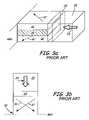
- FIG. 3 ashows a perspective view of a conventional biasing scheme for a tri-layer reader stack, including a backside permanent magnet to provide the biasing field.
- FIG. 3 bshows a top view of a conventional biasing scheme for a tri-layer reader stack, including a backside permanent magnet to provide the biasing field.
- FIG. 4shows a tri-layer reader stack having an in-stack bias layer to provide a biasing field according to the present invention.
- FIG. 5shows a tri-layer reader stack having two in-stack bias layers to provide a biasing field according to the present invention.
- FIG. 6shows a tri-layer reader stack having a magnetic field produced by sense current I to provide a biasing field according to another embodiment of the present invention.
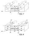
- FIG. 7is a perspective air bearing surface view of a tri-layer reader stack having bias layers positioned on opposite sides of the tri-layer reader stack to provide a biasing field according to another embodiment of the present invention.
- FIG. 8shows a perspective air bearing surface view of a tri-layer reader stack having soft bias stacks positioned on opposite sides of the tri-layer reader stack to provide a biasing field according to another embodiment of the present invention.
- FIG. 1shows a perspective view of tri-layer reader stack 10 in a quiescent/unbiased state.
- Tri-layer reader stack 10includes first free layer 12 , magnetoresistive/spacer layer 14 , and second free layer 16 .
- Magnetoresistive/spacer layer 14is positioned between first free layer 12 and second free layer 16 .
- Free layers 12 and 16are preferably made of a ferromagnetic material.
- Magnetoresistive/spacer layer 14may be either a tunnel barrier (to produce a tunneling magnetoresistive, or TMR, effect) or a nonmagnetic conducting spacer (to produce a giant magnetoresistive, or GMR, effect).
- the quiescent state/unbiased magnetization directions of free layers 12 and 16are denoted by the arrows 12 ′ and 16 ′, respectively, on each of the free layers.
- First free layer 12 and second free layer 16have shape anisotropy induced magnetization directions. That is, the easy axes of magnetization of first free layer 12 and second free layer 16 in a quiescent/unbiased state point in a direction based on the crystal structure of the material.
- First free layer 12is positioned with respect to second free layer 16 in tri-layer reader stack 10 such that the quiescent state/unbiased magnetization directions of the free layers are generally antiparallel with respect to each other.
- the magnetization directions of free layers 12 and 16can also be forced antiparallel with respect to one another by, for example, using permanent magnet biasing or incorporating a pinned antiferromagnetic layer.
- Magnetic alignment between first free layer 12 and second free layer 16is also modifiable by adjusting the size and shape of the free layers. These modifications can be performed as the particular specifications of tri-layer reader stack 10 and the magnetoresistive read/write head dictate.
- the magnetization directions of free layers 12 and 16must be biased generally orthogonal with respect to one another.
- This magnetization configurationallows for greater sensitivity and response to flux emanating from the rotating disc, and allows greater control over the magnetic response of the free layers to magnetic fields.
- the magnetization of first free layer 12is biased orthogonal to the magnetization of second free layer 16 using a permanent magnet abutting a backside of tri-layer reader stack 10 (see FIGS. 3 a and 3 b ).
- FIGS. 2 a , 2 b , and 2 cshow top views of an tri-layer reader stack 10 with proper biasing, provided to show the effect of varying data states (bit flux) on magnetization directions 12 ′ and 16 ′ of first free layer 12 and second free layer 16 , respectively.
- FIG. 2 ashows tri-layer reader stack 10 when it is not under the influence of magnetic flux emanating from the rotating disc. As can be seen, the angle of magnetization between first free layer 12 and second free layer 16 at the ABS is generally orthogonal.
- FIG. 2 bis a top view of tri-layer reader stack 10 , showing tri-layer reader stack 10 under the influence of a first state of data D 1 .
- This first state of datacauses the angle of magnetization between first free layer 12 and second free layer 16 to decrease at the ABS.
- the resistance across tri-layer reader stack 10changes and is detected when a sense current is passed through tri-layer reader stack 10 .
- FIG. 2 cis a top view of tri-layer reader stack 10 , showing tri-layer reader stack 10 under the influence of a second state of data D 2 .
- This second state of datacauses the angle of magnetization between first free layer 12 and second free layer 16 to increase at the ABS.
- the second state of datacauses a change in resistance across tri-layer reader stack 10 and is detected when a sense current is passed through tri-layer reader stack 10 .
- FIG. 3 ashows a perspective view and FIG. 3 b shows a top view of a conventional biasing scheme for tri-layer reader stack 10 , including backside permanent magnet 22 to provide the biasing field.
- Permanent magnet 22is separated from tri-layer reader stack by insulating layer 24 .
- Permanent magnet 22has fixed magnetization direction denoted by arrow 23 on permanent magnet 22 .
- the biased magnetization directions of free layers 12 and 16are denoted by arrows 12 ′ and 16 ′, respectively, on each of the free layers.
- a biasing fieldis needed to bias magnetization 12 ′ of first free layer 12 generally orthogonal with respect to magnetization 16 ′ of free layer 16 .
- This magnetization configurationimproves reader sensitivity and results in greater control over the magnetic response of the reader.
- Positioning of permanent magnet 22 along a back side of tri-layer reader stack 10forces the magnetization directions of free layers 12 and 16 to align at an angle with respect to each other. Different angles between the magnetization directions of free layers 12 and 16 can be achieved by positioning permanent magnet 22 at different distances from tri-layer reader stack 10 by altering a thickness of insulating layer 24 .
- FIG. 4shows tri-layer reader stack 10 having an in-stack bias layer 30 to provide a biasing field according to one embodiment of the present invention.
- Bias layer 30is separated from tri-layer reader stack 10 by nonmagnetic spacer layer 32 .
- Bias layer 30has a fixed magnetization direction, denoted by arrow 33 on bias layer 30 , due to shape anisotropy and the high coercivity of the material which comprises bias layer 30 .
- bias layer 30is a permanent magnet made of, for example, CoCrPt, CoPt or CoPt/SiO 2 .
- bias layer 30is a antiferromagnetic (AFM)/ferromagnetic (FM) bilayer structure, wherein the AFM portion is made of, for example, PtMn, PtPdMn, NiMn, IrMn, or NiO, and the FM portion is made of, for example, CoFe.
- Free layers 12 and 16are preferably made of a ferromagnetic material with good anisotropy such as NiFeCo or CoFeHf.
- the biased magnetization directions of free layers 12 and 16are denoted by arrows 12 ′ and 16 ′, respectively, on each of the free layers.
- bias layer 30With bias layer 30 positioned within tri-layer reader stack 10 , a biasing field is provided to both the front and the back edges of first free layer 12 and second free layer 16 . As shown in FIG. 4 , the biasing fields emerge from the air bearing surface (ABS) side of the bias layer 30 and return to the opposite side of bias layer 30 via free layers 12 and 16 . Bias layer 30 can be positioned to alter the biasing direction with respect to tri-layer reader stack 10 as design requirements dictate. As with the conventional biasing scheme shown in FIGS. 3 a and 3 b , appropriate positioning of bias layer 30 relative to tri-layer reader stack 10 forces the magnetization directions of free layers 12 and 16 to align at an angle with respect to each other.
- ABSair bearing surface
- bias layer 30can be positioned at different distances from tri-layer reader stack 10 (e.g., by varying a thickness of nonmagnetic spacer layer 32 ).
- bias layer 30is positioned such that magnetization direction 12 ′ of first free layer 12 is biased generally orthogonal with respect to magnetization direction 16 ′ of second free layer 16 .
- Nonmagnetic spacer layer 32decouples direct exchange coupling between bias layer 30 and first free layer 12 .
- nonmagnetic spacer layer 32is made of a material that enhances specular reflection of electrons, for example a metal such as Ag and Au, or a metal oxide such as Al 2 O 3 or Y 2 O 3 .
- nonmagnetic spacer layer 32is made of a metal oxide, current shunting through bias layer 30 is eliminated or significantly reduced for current-in-plane (CIP) type sensors. As a result, the sensitivity of the reader will increase. Furthermore, by using a material for nonmagnetic spacer layer 32 that enhances specular reflection of electrons, the magnetoresistive effect produced by magnetoresistive/spacer layer 14 is enhanced, since the mean free path of electrons passing through magnetoresistive/spacer layer 14 is reduced. Specular electron scattering in magnetoresistive devices is discussed in H. J. M. Swagten, G. J. Strijkers, R. H. J. N. Bitter, W. J. M. de Jonge, J. C. S. Kools, Specular Reflection in Spin Valves Bounded by NiO Layers , IEEE Transactions on Magnetics, v. 34, No. 4, pp. 948–953 (1998), and is incorporated by reference.
- FIG. 5shows tri-layer reader stack 10 having in-stack bias layers 40 and 42 to provide a biasing field according to another embodiment of the present invention.
- Bias layers 40 and 42are separated from tri-layer reader stack 10 by nonmagnetic spacer layers 44 and 46 , respectively.
- Bias layer 40has a fixed magnetization direction denoted by arrow 47 and bias layer 42 has a fixed magnetization direction denoted by arrow 48 .
- Bias layers 40 and 42have fixed direction magnetizations due to shape anisotropy and the high coercivity of the material which comprises bias layers 40 and 42 .
- bias layers 40 and 42are antiferromagnetic layers made of, for example, PtMn, PtPdMn, NiMn, IrMn, or NiO, which have pinning directions set by annealing the antiferromagnetic layers in a magnetic field.
- bias layers 40 and 42may alternatively be exchanged coupled in direct contact with free layers 12 and 16 , respectively.
- bias layers 40 and 42are permanent magnets made of, for example, CoCrPt.
- bias layers 40 and 42are antiferromagnetic (AFM)/ferromagnetic (FM) bilayer structures, wherein the AFM portion is made of, for example, PtMn, PtPdMn, NiMn, IrMn, or NiO, and the FM portion is made of, for example, CoFe.
- AFMantiferromagnetic
- FMferromagnetic
- the biased magnetization directions of free layers 12 and 16are denoted by arrows 12 ′ and 16 ′, respectively, on each of the free layers.
- bias layers 40 and 42With bias layers 40 and 42 positioned within tri-layer reader stack 10 , a biasing field is provided to both the front and the back edges of first free layer 12 and second free layer 16 . As shown in FIG. 5 , the biasing fields emerge from the ABS of bias layers 40 and 42 and return to the opposite side of bias layers 40 and 42 via free layers 12 and 16 . Bias layers 40 and 42 can be positioned to alter the biasing direction as reader requirements dictate. As with the conventional biasing scheme shown in FIGS. 3 a and 3 b and the biasing scheme according to the present invention shown in FIG. 4 , appropriate positioning of bias layers 40 and 42 relative to ti-layer reader stack 10 forces the magnetization directions of free layers 12 and 16 to align at an angle with respect to each other.
- bias layers 40 and 42can be positioned at different distances from ti-layer reader stack 10 (e.g., by varying a thickness of nonmagnetic spacer layers 44 and 46 ).
- bias layers 40 and 42are positioned such that the magnetization direction of first free layer 12 is biased generally orthogonal to the magnetization direction of second free layer 16 .
- Nonmagnetic spacer layer 44decouples direct exchange coupling between bias layer 40 and first free layer 12
- nonmagnetic spacer layer 46decouples direct exchange coupling between bias layer 42 and second free layer 16 .
- nonmagnetic spacer layers 44 and 46are made of a material that enhances specular reflection of electrons, for example a metal such as Ag and Au, or a metal oxide such as Al 2 O 3 or Y 2 O 3 . If nonmagnetic spacer layers 44 and 46 are made of a metal oxide, current shunting through bias layer 40 is eliminated or significantly reduced for current-in-plane (CIP) type sensors. As a result, the sensitivity of the reader will increase.
- CIPcurrent-in-plane
- magnetoresistive/spacer layer 14is enhanced, since the mean free path of electrons passing through magnetoresistive/spacer layer 14 is reduced.
- FIG. 6shows tri-layer reader stack 10 having magnetic fields H produced by sense current I to provide a biasing field according to another embodiment of the present invention.
- Sense current leads 60 and 62are connected to tri-layer reader stack 10 via cap layer 64 and seed layer 66 , respectively.
- Sense current Iis passed through sense current leads 60 and 62 and tri-layer reader stack 10 to detect a change in resistivity of the MR sensor (in conjunction with external circuitry as described above and not shown in FIG. 6 ).
- sense current Ipasses through sense current leads 60 and 62
- magnetic fields Hare produced around sense current leads 60 and 62 .
- Magnetic fields Hbias free layers 12 and 16 such that magnetizations 12 ′ and 16 ′ of first free layer 12 and second free layer 16 rotate from their quiescent/unbiased antiparallel state.
- sense current leads 60 and 62With sense current leads 60 and 62 positioned above and below tri-layer reader stack 10 , a biasing field is provided to both the front and back edges of first free layer 12 and second free layer 16 . Additional insulating layers can be positioned between sense current leads 60 and 62 and tri-layer reader 10 to alter the biasing effect magnetic fields H have on free layers 12 and 16 . Appropriate positioning of sense current leads 60 and 62 relative to tri-layer reader stack 10 forces the magnetization directions of free layers 12 and 16 to align at an angle with respect to each other. Different angles between the magnetization directions of free layers 12 and 16 can be achieved by, for example, positioning sense current leads 60 and 62 at different distances from tri-layer reader stack 10 or by varying the magnitude of sense current I. Preferably, sense current leads 60 and 62 and sense current I are configured such that the magnetization direction of first free layer 12 is biased generally orthogonal to the magnetization direction of second free layer 16 .
- FIG. 7shows a perspective air bearing surface view of tri-layer reader stack 10 having bias layers 80 and 82 positioned on opposite sides of tri-layer reader stack 10 to provide a biasing field according to another embodiment of the present invention.
- Bias layers 80 and 82are separated from tri-layer reader stack 10 by nonmagnetic spacer layers 84 and 86 , respectively.
- Bias layer 80has a fixed magnetization direction denoted by arrow 87 and bias layer 82 has a fixed magnetization direction denoted by arrow 88 .
- Cap layer 90 and seed layer 92are positioned on a top and a bottom, respectively, of tri-layer reader stack 10 .
- Bias layers 80 and 82have fixed direction magnetizations due to shape anisotropy and the high coercivity of the material which comprises bias layers 80 and 82 .
- bias layers 80 and 82are permanent magnets made of, for example, CoCrPt.
- bias layers 80 and 82are permanent magnets made of a resistive or insulating material, such as a CoPt/SiO 2 composite.
- bias layers 80 and 82must have a low remnant magnetization (M r ) to avoid erasure of data on the magnetic media due to stray fields from bias layers 80 and 82 at the ABS.
- the biased magnetization directions of free layers 12 and 16are denoted by arrows 12 ′ and 16 ′, respectively, on each of the free layers.
- bias layers 80 and 82With bias layers 80 and 82 positioned on opposite sides of tri-layer reader stack 10 , a biasing field is provided to both the front and the back edges of first free layer 12 and second free layer 16 . As shown in FIG. 7 , the biasing fields emerge from the ABS of bias layers 80 and 82 and pass though tri-layer reader stack 10 (thereby biasing free layers 12 and 16 ). Bias layers 80 and 82 can be positioned to alter the biasing direction as reader requirements dictate. Appropriate positioning of bias layers 80 and 82 relative to tri-layer reader stack 10 forces the magnetization directions of free layers 12 and 16 to align at an angle with respect to each other.
- bias layers 80 and 82can be positioned at different distances from tri-layer reader stack 10 (e.g., by varying a thickness of nonmagnetic spacer layers 84 and 86 ).
- bias layers 80 and 82are positioned such that the magnetization direction of first free layer 12 is biased generally orthogonal to the magnetization direction of second free layer 16 .
- FIG. 8shows a perspective air bearing surface view of tri-layer reader stack 10 having soft bias stacks 100 and 102 positioned on opposite sides of tri-layer reader stack 10 to provide a biasing field according to another embodiment of the present invention.
- Bias stacks 100 and 102are separated from tri-layer reader stack 10 by nonmagnetic spacer layers 104 and 106 , respectively.
- Bias stacks 100 and 102include an antiferromagnetic (AFM)/ferromagnetic (FM)/AFM layer configuration, for example IrMn/CoFe/IrMn stacks.
- AFMantiferromagnetic
- FMferromagnetic
- the AFM layers of bias stacks 100 and 102may be made of an oxide, such as NiO or Fe 3 O 4 , and the FM layers of bias stacks 100 and 102 may be made of a resistive soft magnetic layer, such as Fe 2 O 3 or a CoFe/HfO composite.
- Bias stack 100has a fixed magnetization direction denoted by arrow 107 and bias stack 102 has a fixed magnetization direction denoted by arrow 108 .
- Cap layer 110 and seed layer 112are positioned on a top and a bottom, respectively, of tri-layer reader stack 10 .
- the biased magnetization directions of free layers 12 and 16are denoted by arrows 12 ′ and 16 ′, respectively, on each of the free layers.
- bias stacks 100 and 102With bias stacks 100 and 102 positioned on opposite sides of tri-layer reader stack 10 , a biasing field is provided to both the front and the back edges of first free layer 12 and second free layer 16 . As shown in FIG. 8 , the biasing fields emerge from the ABS of bias stacks 100 and 102 and pass though tri-layer reader stack 10 (thereby biasing free layers 12 and 16 ). Bias stacks 100 and 102 can be positioned to alter the biasing direction as reader requirements dictate. Appropriate positioning of bias stacks 100 and 102 relative to tri-layer reader stack 10 forces the magnetization directions of free layers 12 and 16 to align at an angle with respect to each other.
- bias stacks 100 and 102are positioned such that the magnetization direction of first free layer 12 is biased generally orthogonal to the magnetization direction of second free layer 16 .
- biasing systems of the present inventionoffer several advantages over conventional biasing systems.
- the separation of the bias layer(s) from tri-layer reader stack 10can be readily varied (by varying the thickness of the nonmagnetic spacer layer that separates each bias layer from tri-layer reader stack 10 , for example) to provide the desired biasing field strength and magnetic alignment between free layers 12 and 16 without other design constraints, such as isolating the biasing layer from the remainder of the magnetic read/write head structure.
- both the front edge and the back edge of free layers 12 and 16are subject to the biasing field produced by the bias layer(s). This allows for greater control over the magnetic domains throughout free layers 12 and 16 , thereby offering more control over the magnetic alignment between the two free layers and hysteresis-free magnetization reversal of the free layers.
- the present inventionis a biasing system for a tri-layer reader stack magnetoresistive sensor to provide a biasing field to the entire tri-layer reader stack.
- the tri-layer reader stackincludes a first free layer, a second free layer, and a magnetoresistive/spacer layer between the first and second free layers. Magnetization rotation in the free layers occurs in response to magnetic flux from the disc and a magnetoresistive effect is produced in the nonmagnetic layer.
- the free layersare positioned in the tri-layer reader stack such that quiescent state/unbiased magnetizations of the free layers are substantially antiparallel.
- a biasing structureis positioned with respect to the tri-layer reader stack, typically separated from the tri-layer reader stack by a nonmagnetic spacer layer. The biasing structure produces a biasing field through the tri-layer reader stack. This biasing results in the free layers having biased magnetizations directed at an angle with respect to each other, preferably generally orthogonal.
Landscapes
- Engineering & Computer Science (AREA)
- Manufacturing & Machinery (AREA)
- Magnetic Heads (AREA)
Abstract
Description
Claims (26)
Priority Applications (1)
| Application Number | Priority Date | Filing Date | Title |
|---|---|---|---|
| US10/694,483US7177122B2 (en) | 2003-10-27 | 2003-10-27 | Biasing for tri-layer magnetoresistive sensors |
Applications Claiming Priority (1)
| Application Number | Priority Date | Filing Date | Title |
|---|---|---|---|
| US10/694,483US7177122B2 (en) | 2003-10-27 | 2003-10-27 | Biasing for tri-layer magnetoresistive sensors |
Publications (2)
| Publication Number | Publication Date |
|---|---|
| US20050088789A1 US20050088789A1 (en) | 2005-04-28 |
| US7177122B2true US7177122B2 (en) | 2007-02-13 |
Family
ID=34522613
Family Applications (1)
| Application Number | Title | Priority Date | Filing Date |
|---|---|---|---|
| US10/694,483Expired - Fee RelatedUS7177122B2 (en) | 2003-10-27 | 2003-10-27 | Biasing for tri-layer magnetoresistive sensors |
Country Status (1)
| Country | Link |
|---|---|
| US (1) | US7177122B2 (en) |
Cited By (42)
| Publication number | Priority date | Publication date | Assignee | Title |
|---|---|---|---|---|
| US20060232893A1 (en)* | 2005-04-18 | 2006-10-19 | Hitachi Global Storage Technologies | Current in plane magnetoresistive sensor having a contiguous hard bias layer located at back edge of stripe height |
| US20070035892A1 (en)* | 2003-10-03 | 2007-02-15 | Daniele Pullini | Magnetic transduction sensor device, manufacturing process and detection process therefrom |
| US20070076331A1 (en)* | 2005-10-05 | 2007-04-05 | Hitachi Global Storage Technologies | Magnetoresistive sensor having an improved pinning structure |
| US20070211393A1 (en)* | 2006-03-08 | 2007-09-13 | Gill Hardayal S | Method and apparatus for using a specular scattering layer in a free layer of a magnetic sensor while stabilizing the free layer by direct coupling with an antiferromagnetic layer |
| US20090015252A1 (en)* | 2007-07-13 | 2009-01-15 | Wolfgang Raberg | Magnetoresistive Magnetic Field Sensor Structure |
| US20090109577A1 (en)* | 2007-10-25 | 2009-04-30 | Tdk Corporation | Magneto-resistive effect device of the cpp structure and magnetic disk system |
| US20090128965A1 (en)* | 2007-11-15 | 2009-05-21 | Tomohito Mizuno | Cpp magneto-resistive element provided with a pair of magnetic layers and nicr buffer layer |
| US20090130491A1 (en)* | 2007-11-15 | 2009-05-21 | Tdk Corporation | Magneto-resistive element for a magneto-resistive device and methof of manufacturing thereof |
| US20090180217A1 (en)* | 2008-01-15 | 2009-07-16 | Tdk Corporation | Magneto-resistive effect device of the cpp type, and magnetic disk system |
| US20090190270A1 (en)* | 2008-01-30 | 2009-07-30 | Tdk Corporation | Magneto-resistive effect device of the cpp type, and magnetic disk system |
| US20090190271A1 (en)* | 2008-01-28 | 2009-07-30 | Tdk Corporation | Magnetoresistive element and magnetic head |
| US20090244791A1 (en)* | 2008-03-26 | 2009-10-01 | Tsann Lin | Current-perpendicular-to-plane (cpp) read sensor with multiple ferromagnetic sense layers |
| US7615996B1 (en) | 2009-01-21 | 2009-11-10 | Tdk Corporation | Examination method for CPP-type magnetoresistance effect element having two free layers |
| US20090323222A1 (en)* | 2008-06-30 | 2009-12-31 | Tdk Corporation | Thin film magnetic head, magnetic head slider, head gimbal assembly, head arm assembly, magnetic disk device and method of manufacturing thin film magnetic head |
| US20100085666A1 (en)* | 2008-10-08 | 2010-04-08 | Headway Technologies, Inc. | Low noise magneto-resistive sensor utilizing magnetic noise cancellation |
| US20100214696A1 (en)* | 2009-02-26 | 2010-08-26 | Tdk Corporation | Layered structure having FePt system magnetic layer and magnetoresistive effect element using the same |
| US20110007426A1 (en)* | 2009-07-13 | 2011-01-13 | Seagate Technology Llc | Trapezoidal back bias and trilayer reader geometry to enhance device performance |
| US8289660B2 (en) | 2010-06-16 | 2012-10-16 | Seagate Technology Llc | Auxiliary magnetoresistive shield |
| US8390963B2 (en)* | 2011-04-25 | 2013-03-05 | Seagate Technology Llc | Trilayer reader with current constraint at the ABS |
| CN102997938A (en)* | 2011-09-13 | 2013-03-27 | 希捷科技有限公司 | Tuned shunt ratio for magnetic sensors |
| US8755154B2 (en)* | 2011-09-13 | 2014-06-17 | Seagate Technology Llc | Tuned angled uniaxial anisotropy in trilayer magnetic sensors |
| US8803519B2 (en) | 2011-07-29 | 2014-08-12 | Seagate Technology Llc | Enhanced magnetic sensor biasing yoke |
| US8842394B2 (en) | 2011-10-03 | 2014-09-23 | Kabushiki Kaisha Toshiba | Magnetic head |
| US8879214B2 (en) | 2011-12-21 | 2014-11-04 | HGST Netherlands B.V. | Half metal trilayer TMR reader with negative interlayer coupling |
| US8879213B2 (en) | 2012-08-16 | 2014-11-04 | Kabushiki Kaisha Toshiba | Magneto-resistance effect element, magnetic head, magnetic head assembly, magnetic recording and reproducing apparatus, and method for manufacturing magneto-resistance effect element |
| US8907666B2 (en) | 2011-09-30 | 2014-12-09 | HGST Netherlands B.V. | Magnetic bias structure for magnetoresistive sensor having a scissor structure |
| US8922950B2 (en) | 2011-05-06 | 2014-12-30 | Seagate Technology Llc | Multi-layer magnetoresistive shield with transition metal layer |
| US9041391B2 (en) | 2011-07-29 | 2015-05-26 | Seagate Technology Llc | Partial magnetic biasing of magnetoresistive sensor |
| US20150145081A1 (en)* | 2010-07-26 | 2015-05-28 | Sechung Oh | Magnetic memory devices having a uniform perpendicular nonmagnetic rich antisotropy enhanced pattern |
| US9076468B1 (en)* | 2014-03-12 | 2015-07-07 | HGST Netherlands B.V. | Scissor magnetic read sensor with shape enhanced soft magnetic side shield for improved stability |
| US9799356B2 (en) | 2016-01-04 | 2017-10-24 | Western Digital Technologies, Inc. | Coupled soft bias scissor type sensor |
| US10270853B2 (en) | 2016-07-22 | 2019-04-23 | Fisher-Rosemount Systems, Inc. | Process control communication between a portable field maintenance tool and an asset management system |
| US10375162B2 (en) | 2016-07-22 | 2019-08-06 | Fisher-Rosemount Systems, Inc. | Process control communication architecture |
| US10374873B2 (en) | 2016-07-22 | 2019-08-06 | Fisher-Rosemount Systems, Inc. | Process control communication between a portable field maintenance tool and a process control instrument |
| US10382312B2 (en) | 2016-03-02 | 2019-08-13 | Fisher-Rosemount Systems, Inc. | Detecting and locating process control communication line faults from a handheld maintenance tool |
| US10481627B2 (en) | 2016-07-25 | 2019-11-19 | Fisher-Rosemount Systems, Inc. | Connection check in field maintenance tool |
| US10505585B2 (en) | 2016-07-25 | 2019-12-10 | Fisher-Rosemount Systems, Inc. | Portable field maintenance tool with a bus for powering and communicating with a field device |
| US10554644B2 (en) | 2016-07-20 | 2020-02-04 | Fisher-Rosemount Systems, Inc. | Two-factor authentication for user interface devices in a process plant |
| US10585422B2 (en) | 2016-07-22 | 2020-03-10 | Fisher-Rosemount Systems, Inc. | Portable field maintenance tool system having interchangeable functional modules |
| US10599134B2 (en) | 2016-07-22 | 2020-03-24 | Fisher-Rosemount Systems, Inc. | Portable field maintenance tool configured for multiple process control communication protocols |
| US10764083B2 (en) | 2016-07-25 | 2020-09-01 | Fisher-Rosemount Systems, Inc. | Portable field maintenance tool with resistor network for intrinsically safe operation |
| US11605037B2 (en) | 2016-07-20 | 2023-03-14 | Fisher-Rosemount Systems, Inc. | Fleet management system for portable maintenance tools |
Families Citing this family (20)
| Publication number | Priority date | Publication date | Assignee | Title |
|---|---|---|---|---|
| US6735112B2 (en)* | 2002-02-06 | 2004-05-11 | Micron Technology, Inc. | Magneto-resistive memory cell structures with improved selectivity |
| US7301735B2 (en)* | 2004-03-15 | 2007-11-27 | Hitachi Global Technologies Netherlands B.V. | Higher flip threshold structure for in-stack bias layer |
| US7602591B2 (en)* | 2005-06-22 | 2009-10-13 | Tdk Corporation | Exchange-coupled free layer with out-of-plane magnetization |
| JP4358279B2 (en) | 2007-08-22 | 2009-11-04 | 株式会社東芝 | Magnetic recording head and magnetic recording apparatus |
| JP2009070439A (en)* | 2007-09-11 | 2009-04-02 | Toshiba Corp | Magnetic recording head and magnetic recording apparatus |
| JP2009080875A (en) | 2007-09-25 | 2009-04-16 | Toshiba Corp | Magnetic head and magnetic recording apparatus |
| JP5361259B2 (en)* | 2008-06-19 | 2013-12-04 | 株式会社東芝 | Spin torque oscillator, magnetic recording head, magnetic head assembly, and magnetic recording apparatus |
| JP2010040060A (en)* | 2008-07-31 | 2010-02-18 | Toshiba Corp | Magnetic head for high-frequency field assist recording and magnetic recording apparatus using the same |
| JP5558698B2 (en) | 2008-11-28 | 2014-07-23 | 株式会社東芝 | Magnetic recording head, magnetic head assembly, magnetic recording apparatus, and magnetic recording method |
| US20110026169A1 (en)* | 2009-07-28 | 2011-02-03 | Hardayal Singh Gill | Dual cpp gmr head using a scissor sensor |
| US8582250B2 (en)* | 2009-12-04 | 2013-11-12 | Seagate Technology Llc | Double biasing for trilayer MR sensors |
| JP5443421B2 (en) | 2011-03-24 | 2014-03-19 | 株式会社東芝 | Magnetoresistive element, magnetic head gimbal assembly, and magnetic recording / reproducing apparatus |
| US20120327537A1 (en) | 2011-06-23 | 2012-12-27 | Seagate Technology Llc | Shield Stabilization Configuration With Applied Bias |
| US9036308B2 (en)* | 2011-09-21 | 2015-05-19 | Seagate Technology Llc | Varyinig morphology in magnetic sensor sub-layers |
| JP5606482B2 (en) | 2012-03-26 | 2014-10-15 | 株式会社東芝 | Magnetic head, magnetic head assembly, magnetic recording / reproducing apparatus, and magnetic head manufacturing method |
| US20140355152A1 (en)* | 2013-05-29 | 2014-12-04 | HGST Netherlands B.V. | Interlayer coupled free layer with out of plane magnetic orientation for magnetic read head |
| JP6523004B2 (en)* | 2015-03-24 | 2019-05-29 | 株式会社東芝 | Strain sensing element and pressure sensor |
| JP6107864B2 (en)* | 2015-03-26 | 2017-04-05 | Tdk株式会社 | Magnetic sensor and magnetic encoder |
| EP3875913B1 (en)* | 2020-03-04 | 2023-10-25 | Melexis Technologies SA | Hybrid position sensor |
| CN115542208A (en)* | 2022-10-26 | 2022-12-30 | 南方电网数字电网研究院有限公司 | A magnetoresistive sensor based on titanium dioxide three-layer structure |
Citations (20)
| Publication number | Priority date | Publication date | Assignee | Title |
|---|---|---|---|---|
| US5576914A (en) | 1994-11-14 | 1996-11-19 | Read-Rite Corporation | Compact read/write head having biased GMR element |
| US5664316A (en) | 1995-01-17 | 1997-09-09 | International Business Machines Corporation | Method of manufacturing magnetoresistive read transducer having a contiguous longitudinal bias layer |
| US5736060A (en) | 1992-08-25 | 1998-04-07 | Seagate Technology, Inc. | Read sensitivity MR head using permanent magnet longitudinal stabilization |
| US5739987A (en) | 1996-06-04 | 1998-04-14 | Read-Rite Corporation | Magnetoresistive read transducers with multiple longitudinal stabilization layers |
| US5739990A (en) | 1996-11-13 | 1998-04-14 | Read-Rite Corporation | Spin-valve GMR sensor with inbound exchange stabilization |
| US5959809A (en)* | 1994-07-29 | 1999-09-28 | Fujitsu Limited | Magnetoresistive head and method of manufacturing the same and magnetic recording apparatus |
| US6005753A (en) | 1998-05-29 | 1999-12-21 | International Business Machines Corporation | Magnetic tunnel junction magnetoresistive read head with longitudinal and transverse bias |
| US6023395A (en) | 1998-05-29 | 2000-02-08 | International Business Machines Corporation | Magnetic tunnel junction magnetoresistive sensor with in-stack biasing |
| US6046891A (en)* | 1992-11-30 | 2000-04-04 | Kabushiki Kaisha Toshiba | Thin film head |
| US6087026A (en)* | 1997-06-04 | 2000-07-11 | Fujitsu Limited | Magnetoresistive head and magnetic read/write device |
| US6114719A (en) | 1998-05-29 | 2000-09-05 | International Business Machines Corporation | Magnetic tunnel junction memory cell with in-stack biasing of the free ferromagnetic layer and memory array using the cell |
| US6154350A (en)* | 1997-12-30 | 2000-11-28 | Samsung Electronics Co., Ltd. | Soft adjacent layer-biased magnetoresistive head and method |
| US6255814B1 (en)* | 1998-08-11 | 2001-07-03 | Tdk Corporation | Method and apparatus for measuring bias magnetic field for controlling magnetic domain of magnetoresistive effect element |
| US6266218B1 (en)* | 1999-10-28 | 2001-07-24 | International Business Machines Corporation | Magnetic sensors having antiferromagnetically exchange-coupled layers for longitudinal biasing |
| US6324037B1 (en) | 1999-07-26 | 2001-11-27 | Headway Technologies, Inc. | Magnetically stable spin-valve sensor |
| US6353316B1 (en)* | 1998-06-18 | 2002-03-05 | Tdk Corporation | Magneto-resistive element and thin film magnetic head comprising the same |
| US6396734B2 (en) | 1999-08-26 | 2002-05-28 | Hitachi, Ltd. | Giant magnetoresistive sensor, thin-film read/write head and magnetic recording apparatus using the sensor |
| US20020114111A1 (en) | 2001-02-20 | 2002-08-22 | Jian-Gang Zhu | High density magnetoresistive read head |
| US6449131B2 (en)* | 1998-10-30 | 2002-09-10 | Headway Technologies, Inc. | Canted longitudinal patterned exchange biased dual-stripe magnetoresistive (DSMR) sensor element and method for fabrication thereof |
| US20020167768A1 (en) | 2001-05-11 | 2002-11-14 | International Business Machines Corporation | CPP magnetoresistive sensors with in-stack longitudinal biasing and overlapping magnetic shield |
- 2003
- 2003-10-27USUS10/694,483patent/US7177122B2/ennot_activeExpired - Fee Related
Patent Citations (21)
| Publication number | Priority date | Publication date | Assignee | Title |
|---|---|---|---|---|
| US5736060A (en) | 1992-08-25 | 1998-04-07 | Seagate Technology, Inc. | Read sensitivity MR head using permanent magnet longitudinal stabilization |
| US5737155A (en) | 1992-08-25 | 1998-04-07 | Seagate Technology, Inc. | Read sensitivity MR head using permanent magnet longitudinal stabilization |
| US6046891A (en)* | 1992-11-30 | 2000-04-04 | Kabushiki Kaisha Toshiba | Thin film head |
| US5959809A (en)* | 1994-07-29 | 1999-09-28 | Fujitsu Limited | Magnetoresistive head and method of manufacturing the same and magnetic recording apparatus |
| US5576914A (en) | 1994-11-14 | 1996-11-19 | Read-Rite Corporation | Compact read/write head having biased GMR element |
| US5664316A (en) | 1995-01-17 | 1997-09-09 | International Business Machines Corporation | Method of manufacturing magnetoresistive read transducer having a contiguous longitudinal bias layer |
| US5739987A (en) | 1996-06-04 | 1998-04-14 | Read-Rite Corporation | Magnetoresistive read transducers with multiple longitudinal stabilization layers |
| US5739990A (en) | 1996-11-13 | 1998-04-14 | Read-Rite Corporation | Spin-valve GMR sensor with inbound exchange stabilization |
| US6087026A (en)* | 1997-06-04 | 2000-07-11 | Fujitsu Limited | Magnetoresistive head and magnetic read/write device |
| US6154350A (en)* | 1997-12-30 | 2000-11-28 | Samsung Electronics Co., Ltd. | Soft adjacent layer-biased magnetoresistive head and method |
| US6023395A (en) | 1998-05-29 | 2000-02-08 | International Business Machines Corporation | Magnetic tunnel junction magnetoresistive sensor with in-stack biasing |
| US6005753A (en) | 1998-05-29 | 1999-12-21 | International Business Machines Corporation | Magnetic tunnel junction magnetoresistive read head with longitudinal and transverse bias |
| US6114719A (en) | 1998-05-29 | 2000-09-05 | International Business Machines Corporation | Magnetic tunnel junction memory cell with in-stack biasing of the free ferromagnetic layer and memory array using the cell |
| US6353316B1 (en)* | 1998-06-18 | 2002-03-05 | Tdk Corporation | Magneto-resistive element and thin film magnetic head comprising the same |
| US6255814B1 (en)* | 1998-08-11 | 2001-07-03 | Tdk Corporation | Method and apparatus for measuring bias magnetic field for controlling magnetic domain of magnetoresistive effect element |
| US6449131B2 (en)* | 1998-10-30 | 2002-09-10 | Headway Technologies, Inc. | Canted longitudinal patterned exchange biased dual-stripe magnetoresistive (DSMR) sensor element and method for fabrication thereof |
| US6324037B1 (en) | 1999-07-26 | 2001-11-27 | Headway Technologies, Inc. | Magnetically stable spin-valve sensor |
| US6396734B2 (en) | 1999-08-26 | 2002-05-28 | Hitachi, Ltd. | Giant magnetoresistive sensor, thin-film read/write head and magnetic recording apparatus using the sensor |
| US6266218B1 (en)* | 1999-10-28 | 2001-07-24 | International Business Machines Corporation | Magnetic sensors having antiferromagnetically exchange-coupled layers for longitudinal biasing |
| US20020114111A1 (en) | 2001-02-20 | 2002-08-22 | Jian-Gang Zhu | High density magnetoresistive read head |
| US20020167768A1 (en) | 2001-05-11 | 2002-11-14 | International Business Machines Corporation | CPP magnetoresistive sensors with in-stack longitudinal biasing and overlapping magnetic shield |
Cited By (62)
| Publication number | Priority date | Publication date | Assignee | Title |
|---|---|---|---|---|
| US20070035892A1 (en)* | 2003-10-03 | 2007-02-15 | Daniele Pullini | Magnetic transduction sensor device, manufacturing process and detection process therefrom |
| US7451641B2 (en)* | 2003-10-03 | 2008-11-18 | C.R.F. Società Consortile Per Azioni | Magnetic transduction sensor device, manufacturing process and detection process therefrom |
| US7369374B2 (en)* | 2005-04-18 | 2008-05-06 | Hitachi Global Storage Technologies Netherlands B.V. | Current in plane magnetoresistive sensor having a contiguous hard bias layer located at back edge of stripe height |
| US20060232893A1 (en)* | 2005-04-18 | 2006-10-19 | Hitachi Global Storage Technologies | Current in plane magnetoresistive sensor having a contiguous hard bias layer located at back edge of stripe height |
| US20070076331A1 (en)* | 2005-10-05 | 2007-04-05 | Hitachi Global Storage Technologies | Magnetoresistive sensor having an improved pinning structure |
| US7436637B2 (en)* | 2005-10-05 | 2008-10-14 | Hitachi Global Storage Technologies Netherlands B.V. | Magnetoresistive sensor having an improved pinning structure |
| US7626787B2 (en)* | 2006-03-08 | 2009-12-01 | Hitachi Global Storage Technologies Netherlands B.V. | Method and apparatus for using a specular scattering layer in a free layer of a magnetic sensor while stabilizing the free layer by direct coupling with an antiferromagnetic layer |
| US20070211393A1 (en)* | 2006-03-08 | 2007-09-13 | Gill Hardayal S | Method and apparatus for using a specular scattering layer in a free layer of a magnetic sensor while stabilizing the free layer by direct coupling with an antiferromagnetic layer |
| US20090015252A1 (en)* | 2007-07-13 | 2009-01-15 | Wolfgang Raberg | Magnetoresistive Magnetic Field Sensor Structure |
| US8063633B2 (en)* | 2007-07-13 | 2011-11-22 | Infineon Technologies Ag | Magnetoresistive magnetic field sensor structure |
| US20090109577A1 (en)* | 2007-10-25 | 2009-04-30 | Tdk Corporation | Magneto-resistive effect device of the cpp structure and magnetic disk system |
| US7894166B2 (en) | 2007-10-25 | 2011-02-22 | Tdk Corporation | CPP GMR device with ferromagnetic layer split in depth direction |
| US20090128965A1 (en)* | 2007-11-15 | 2009-05-21 | Tomohito Mizuno | Cpp magneto-resistive element provided with a pair of magnetic layers and nicr buffer layer |
| US8310792B2 (en)* | 2007-11-15 | 2012-11-13 | Tdk Corporation | Magneto-resistive element for a magneto-resistive device and method of manufacturing thereof |
| US20090130491A1 (en)* | 2007-11-15 | 2009-05-21 | Tdk Corporation | Magneto-resistive element for a magneto-resistive device and methof of manufacturing thereof |
| US20090180217A1 (en)* | 2008-01-15 | 2009-07-16 | Tdk Corporation | Magneto-resistive effect device of the cpp type, and magnetic disk system |
| US7876534B2 (en) | 2008-01-15 | 2011-01-25 | Tdk Corporation | Magneto-resistive effect device of the CPP type, and magnetic disk system |
| US20090190271A1 (en)* | 2008-01-28 | 2009-07-30 | Tdk Corporation | Magnetoresistive element and magnetic head |
| US7952839B2 (en) | 2008-01-28 | 2011-05-31 | Tdk Corporation | Magnetoresistive element including an antiferromagnetic layer disposed away from a detection surface |
| US20090190270A1 (en)* | 2008-01-30 | 2009-07-30 | Tdk Corporation | Magneto-resistive effect device of the cpp type, and magnetic disk system |
| US7881021B2 (en)* | 2008-01-30 | 2011-02-01 | Tdk Corporation | CPP type magnetoresistive device with biasing arrangement for ferromagnetic layers having respective magnetizations orthogonal to one another, and magnetic disk system using same |
| US20090244791A1 (en)* | 2008-03-26 | 2009-10-01 | Tsann Lin | Current-perpendicular-to-plane (cpp) read sensor with multiple ferromagnetic sense layers |
| US8164863B2 (en) | 2008-03-26 | 2012-04-24 | Hitachi Global Storage Technologies Netherlands B.V. | Current-perpendicular-to-plane (CPP) read sensor with multiple ferromagnetic sense layers |
| US20090323222A1 (en)* | 2008-06-30 | 2009-12-31 | Tdk Corporation | Thin film magnetic head, magnetic head slider, head gimbal assembly, head arm assembly, magnetic disk device and method of manufacturing thin film magnetic head |
| US8427790B2 (en) | 2008-06-30 | 2013-04-23 | Tdk Corporation | Thin film magnetic head having similarly structured resistive film pattern and magnetic bias layer |
| US8031445B2 (en) | 2008-10-08 | 2011-10-04 | Headway Technologies, Inc. | Low noise magneto-resistive sensor utilizing magnetic noise cancellation |
| US20100085666A1 (en)* | 2008-10-08 | 2010-04-08 | Headway Technologies, Inc. | Low noise magneto-resistive sensor utilizing magnetic noise cancellation |
| US7615996B1 (en) | 2009-01-21 | 2009-11-10 | Tdk Corporation | Examination method for CPP-type magnetoresistance effect element having two free layers |
| US20100214696A1 (en)* | 2009-02-26 | 2010-08-26 | Tdk Corporation | Layered structure having FePt system magnetic layer and magnetoresistive effect element using the same |
| US8147994B2 (en)* | 2009-02-26 | 2012-04-03 | Tdk Corporation | Layered structure having FePt system magnetic layer and magnetoresistive effect element using the same |
| US20110007426A1 (en)* | 2009-07-13 | 2011-01-13 | Seagate Technology Llc | Trapezoidal back bias and trilayer reader geometry to enhance device performance |
| US8724265B2 (en) | 2009-07-13 | 2014-05-13 | Seagate Technology Llc | Trapezoidal back bias and trilayer reader geometry with predetermined magnetization shape |
| US8289660B2 (en) | 2010-06-16 | 2012-10-16 | Seagate Technology Llc | Auxiliary magnetoresistive shield |
| US9318695B2 (en)* | 2010-07-26 | 2016-04-19 | Samsung Electronics Co., Ltd. | Magnetic memory devices having a uniform perpendicular nonmagnetic rich antisotropy enhanced pattern |
| US20150145081A1 (en)* | 2010-07-26 | 2015-05-28 | Sechung Oh | Magnetic memory devices having a uniform perpendicular nonmagnetic rich antisotropy enhanced pattern |
| US8390963B2 (en)* | 2011-04-25 | 2013-03-05 | Seagate Technology Llc | Trilayer reader with current constraint at the ABS |
| US8922950B2 (en) | 2011-05-06 | 2014-12-30 | Seagate Technology Llc | Multi-layer magnetoresistive shield with transition metal layer |
| US8803519B2 (en) | 2011-07-29 | 2014-08-12 | Seagate Technology Llc | Enhanced magnetic sensor biasing yoke |
| US9041391B2 (en) | 2011-07-29 | 2015-05-26 | Seagate Technology Llc | Partial magnetic biasing of magnetoresistive sensor |
| US8755154B2 (en)* | 2011-09-13 | 2014-06-17 | Seagate Technology Llc | Tuned angled uniaxial anisotropy in trilayer magnetic sensors |
| CN102997938A (en)* | 2011-09-13 | 2013-03-27 | 希捷科技有限公司 | Tuned shunt ratio for magnetic sensors |
| CN102997938B (en)* | 2011-09-13 | 2015-10-21 | 希捷科技有限公司 | For the split ratio through adjustment of Magnetic Sensor |
| US8749924B2 (en) | 2011-09-13 | 2014-06-10 | Seagate Technology Llc | Tuned shunt ratio for magnetic sensors |
| US8907666B2 (en) | 2011-09-30 | 2014-12-09 | HGST Netherlands B.V. | Magnetic bias structure for magnetoresistive sensor having a scissor structure |
| US8842394B2 (en) | 2011-10-03 | 2014-09-23 | Kabushiki Kaisha Toshiba | Magnetic head |
| US8879214B2 (en) | 2011-12-21 | 2014-11-04 | HGST Netherlands B.V. | Half metal trilayer TMR reader with negative interlayer coupling |
| US8879213B2 (en) | 2012-08-16 | 2014-11-04 | Kabushiki Kaisha Toshiba | Magneto-resistance effect element, magnetic head, magnetic head assembly, magnetic recording and reproducing apparatus, and method for manufacturing magneto-resistance effect element |
| US9076468B1 (en)* | 2014-03-12 | 2015-07-07 | HGST Netherlands B.V. | Scissor magnetic read sensor with shape enhanced soft magnetic side shield for improved stability |
| US9799356B2 (en) | 2016-01-04 | 2017-10-24 | Western Digital Technologies, Inc. | Coupled soft bias scissor type sensor |
| US10096331B2 (en) | 2016-01-04 | 2018-10-09 | Western Digital Technologies, Inc. | Coupled soft bias scissor type sensor |
| US10382312B2 (en) | 2016-03-02 | 2019-08-13 | Fisher-Rosemount Systems, Inc. | Detecting and locating process control communication line faults from a handheld maintenance tool |
| US11368384B2 (en) | 2016-03-02 | 2022-06-21 | Fisher-Rosemount Systems, Inc. | Detecting and locating process control communication line faults from a handheld maintenance tool |
| US10554644B2 (en) | 2016-07-20 | 2020-02-04 | Fisher-Rosemount Systems, Inc. | Two-factor authentication for user interface devices in a process plant |
| US11605037B2 (en) | 2016-07-20 | 2023-03-14 | Fisher-Rosemount Systems, Inc. | Fleet management system for portable maintenance tools |
| US10374873B2 (en) | 2016-07-22 | 2019-08-06 | Fisher-Rosemount Systems, Inc. | Process control communication between a portable field maintenance tool and a process control instrument |
| US10375162B2 (en) | 2016-07-22 | 2019-08-06 | Fisher-Rosemount Systems, Inc. | Process control communication architecture |
| US10585422B2 (en) | 2016-07-22 | 2020-03-10 | Fisher-Rosemount Systems, Inc. | Portable field maintenance tool system having interchangeable functional modules |
| US10599134B2 (en) | 2016-07-22 | 2020-03-24 | Fisher-Rosemount Systems, Inc. | Portable field maintenance tool configured for multiple process control communication protocols |
| US10270853B2 (en) | 2016-07-22 | 2019-04-23 | Fisher-Rosemount Systems, Inc. | Process control communication between a portable field maintenance tool and an asset management system |
| US10481627B2 (en) | 2016-07-25 | 2019-11-19 | Fisher-Rosemount Systems, Inc. | Connection check in field maintenance tool |
| US10505585B2 (en) | 2016-07-25 | 2019-12-10 | Fisher-Rosemount Systems, Inc. | Portable field maintenance tool with a bus for powering and communicating with a field device |
| US10764083B2 (en) | 2016-07-25 | 2020-09-01 | Fisher-Rosemount Systems, Inc. | Portable field maintenance tool with resistor network for intrinsically safe operation |
Also Published As
| Publication number | Publication date |
|---|---|
| US20050088789A1 (en) | 2005-04-28 |
Similar Documents
| Publication | Publication Date | Title |
|---|---|---|
| US7177122B2 (en) | Biasing for tri-layer magnetoresistive sensors | |
| US6947264B2 (en) | Self-pinned in-stack bias structure for magnetoresistive read heads | |
| US7477490B2 (en) | Single sensor element that is naturally differentiated | |
| US7428126B2 (en) | Domain wall free shields of MR sensors | |
| US20110134572A1 (en) | Double biasing for trilayer mr sensors | |
| US20110007426A1 (en) | Trapezoidal back bias and trilayer reader geometry to enhance device performance | |
| US20140104729A1 (en) | Shield Stabilization Configuration with Applied Bias | |
| US7298597B2 (en) | Magnetoresistive sensor based on spin accumulation effect with free layer stabilized by in-stack orthogonal magnetic coupling | |
| US6191926B1 (en) | Spin valve magnetoresistive sensor using permanent magnet biased artificial antiferromagnet layer | |
| JP4778328B2 (en) | Magnetic sensor with in-stack biasing structure | |
| JP2000276720A (en) | Dual stripe spin valve sensor without antiferromagnetic pinning layer | |
| US7016160B2 (en) | Differential CPP reader for perpendicular magnetic recording | |
| US8520344B2 (en) | Magnetoresistive device with enhanced pinned layer | |
| US7019949B2 (en) | Self-pinned spin valve sensor having its first AP pinned layer thicker than its second AP pinned layer to reduce the likelihood of amplitude flip | |
| US6762915B2 (en) | Magnetoresistive sensor with oversized pinned layer | |
| US7038889B2 (en) | Method and apparatus for enhanced dual spin valve giant magnetoresistance effects having second spin valve self-pinned composite layer | |
| US20090080125A1 (en) | Magnetic head | |
| US20050018361A1 (en) | Apparatus for extended self-pinned layer for a current perpendicular to plane head | |
| US7171741B2 (en) | Method for extended self-pinned layer for a current perpendicular to plane head | |
| US20150213815A1 (en) | Synthetic antiferromagnetic reader | |
| US10249329B1 (en) | Current-perpendicular-to-the-plane (CPP) magnetoresistive (MR) sensor with wedge shaped free layer | |
| US7271986B2 (en) | V-shape magnetic field sensor with anisotropy induced orthogonal magnetic alignment | |
| US6169647B1 (en) | Giant magnetoresistive sensor having weakly pinned ferromagnetic layer | |
| US6426853B1 (en) | Magnetoresistive effect sensor, thin-film magnetic head and thin-film wafer with the thin-film magnetic heads | |
| US6713800B2 (en) | Magnetoresistive sensor with reduced side-reading effect |
Legal Events
| Date | Code | Title | Description |
|---|---|---|---|
| AS | Assignment | Owner name:SEAGATE TECHNOLOGY LLC, CALIFORNIA Free format text:ASSIGNMENT OF ASSIGNORS INTEREST;ASSIGNORS:HOU, CHUNHONG;MAO, SINING;LINVILLE, ERIC S.;AND OTHERS;REEL/FRAME:014648/0721;SIGNING DATES FROM 20031003 TO 20031008 | |
| AS | Assignment | Owner name:SEAGATE TECHNOLOGY LLC, CALIFORNIA Free format text:RE-RECORD TO CORRECT THE LIST OF INVENTORS IN AN ASSIGNMENT DOCUMENT PREVIOUSLY RECORDED ON REEL 014648 FRAME 0721.;ASSIGNORS:HOU, CHUNHONG;MAO, SINING;LINVILLE, ERIC S.;AND OTHERS;REEL/FRAME:015483/0401;SIGNING DATES FROM 20031003 TO 20031008 | |
| AS | Assignment | Owner name:WELLS FARGO BANK, NATIONAL ASSOCIATION, AS COLLATERAL AGENT AND SECOND PRIORITY REPRESENTATIVE, CALIFORNIA Free format text:SECURITY AGREEMENT;ASSIGNORS:MAXTOR CORPORATION;SEAGATE TECHNOLOGY LLC;SEAGATE TECHNOLOGY INTERNATIONAL;REEL/FRAME:022757/0017 Effective date:20090507 Owner name:JPMORGAN CHASE BANK, N.A., AS ADMINISTRATIVE AGENT AND FIRST PRIORITY REPRESENTATIVE, NEW YORK Free format text:SECURITY AGREEMENT;ASSIGNORS:MAXTOR CORPORATION;SEAGATE TECHNOLOGY LLC;SEAGATE TECHNOLOGY INTERNATIONAL;REEL/FRAME:022757/0017 Effective date:20090507 Owner name:JPMORGAN CHASE BANK, N.A., AS ADMINISTRATIVE AGENT Free format text:SECURITY AGREEMENT;ASSIGNORS:MAXTOR CORPORATION;SEAGATE TECHNOLOGY LLC;SEAGATE TECHNOLOGY INTERNATIONAL;REEL/FRAME:022757/0017 Effective date:20090507 Owner name:WELLS FARGO BANK, NATIONAL ASSOCIATION, AS COLLATE Free format text:SECURITY AGREEMENT;ASSIGNORS:MAXTOR CORPORATION;SEAGATE TECHNOLOGY LLC;SEAGATE TECHNOLOGY INTERNATIONAL;REEL/FRAME:022757/0017 Effective date:20090507 | |
| FPAY | Fee payment | Year of fee payment:4 | |
| AS | Assignment | Owner name:SEAGATE TECHNOLOGY LLC, CALIFORNIA Free format text:RELEASE;ASSIGNOR:JPMORGAN CHASE BANK, N.A., AS ADMINISTRATIVE AGENT;REEL/FRAME:025662/0001 Effective date:20110114 Owner name:MAXTOR CORPORATION, CALIFORNIA Free format text:RELEASE;ASSIGNOR:JPMORGAN CHASE BANK, N.A., AS ADMINISTRATIVE AGENT;REEL/FRAME:025662/0001 Effective date:20110114 Owner name:SEAGATE TECHNOLOGY HDD HOLDINGS, CALIFORNIA Free format text:RELEASE;ASSIGNOR:JPMORGAN CHASE BANK, N.A., AS ADMINISTRATIVE AGENT;REEL/FRAME:025662/0001 Effective date:20110114 Owner name:SEAGATE TECHNOLOGY INTERNATIONAL, CALIFORNIA Free format text:RELEASE;ASSIGNOR:JPMORGAN CHASE BANK, N.A., AS ADMINISTRATIVE AGENT;REEL/FRAME:025662/0001 Effective date:20110114 | |
| AS | Assignment | Owner name:THE BANK OF NOVA SCOTIA, AS ADMINISTRATIVE AGENT, CANADA Free format text:SECURITY AGREEMENT;ASSIGNOR:SEAGATE TECHNOLOGY LLC;REEL/FRAME:026010/0350 Effective date:20110118 Owner name:THE BANK OF NOVA SCOTIA, AS ADMINISTRATIVE AGENT, Free format text:SECURITY AGREEMENT;ASSIGNOR:SEAGATE TECHNOLOGY LLC;REEL/FRAME:026010/0350 Effective date:20110118 | |
| AS | Assignment | Owner name:SEAGATE TECHNOLOGY INTERNATIONAL, CAYMAN ISLANDS Free format text:TERMINATION AND RELEASE OF SECURITY INTEREST IN PATENT RIGHTS;ASSIGNOR:WELLS FARGO BANK, NATIONAL ASSOCIATION, AS COLLATERAL AGENT AND SECOND PRIORITY REPRESENTATIVE;REEL/FRAME:030833/0001 Effective date:20130312 Owner name:SEAGATE TECHNOLOGY US HOLDINGS, INC., CALIFORNIA Free format text:TERMINATION AND RELEASE OF SECURITY INTEREST IN PATENT RIGHTS;ASSIGNOR:WELLS FARGO BANK, NATIONAL ASSOCIATION, AS COLLATERAL AGENT AND SECOND PRIORITY REPRESENTATIVE;REEL/FRAME:030833/0001 Effective date:20130312 Owner name:EVAULT INC. (F/K/A I365 INC.), CALIFORNIA Free format text:TERMINATION AND RELEASE OF SECURITY INTEREST IN PATENT RIGHTS;ASSIGNOR:WELLS FARGO BANK, NATIONAL ASSOCIATION, AS COLLATERAL AGENT AND SECOND PRIORITY REPRESENTATIVE;REEL/FRAME:030833/0001 Effective date:20130312 Owner name:SEAGATE TECHNOLOGY LLC, CALIFORNIA Free format text:TERMINATION AND RELEASE OF SECURITY INTEREST IN PATENT RIGHTS;ASSIGNOR:WELLS FARGO BANK, NATIONAL ASSOCIATION, AS COLLATERAL AGENT AND SECOND PRIORITY REPRESENTATIVE;REEL/FRAME:030833/0001 Effective date:20130312 | |
| FPAY | Fee payment | Year of fee payment:8 | |
| FEPP | Fee payment procedure | Free format text:MAINTENANCE FEE REMINDER MAILED (ORIGINAL EVENT CODE: REM.); ENTITY STATUS OF PATENT OWNER: LARGE ENTITY | |
| LAPS | Lapse for failure to pay maintenance fees | Free format text:PATENT EXPIRED FOR FAILURE TO PAY MAINTENANCE FEES (ORIGINAL EVENT CODE: EXP.); ENTITY STATUS OF PATENT OWNER: LARGE ENTITY | |
| STCH | Information on status: patent discontinuation | Free format text:PATENT EXPIRED DUE TO NONPAYMENT OF MAINTENANCE FEES UNDER 37 CFR 1.362 | |
| FP | Lapsed due to failure to pay maintenance fee | Effective date:20190213 | |
| AS | Assignment | Owner name:SEAGATE TECHNOLOGY PUBLIC LIMITED COMPANY, CALIFORNIA Free format text:RELEASE BY SECURED PARTY;ASSIGNOR:THE BANK OF NOVA SCOTIA;REEL/FRAME:072193/0001 Effective date:20250303 Owner name:SEAGATE TECHNOLOGY, CALIFORNIA Free format text:RELEASE BY SECURED PARTY;ASSIGNOR:THE BANK OF NOVA SCOTIA;REEL/FRAME:072193/0001 Effective date:20250303 Owner name:SEAGATE TECHNOLOGY HDD HOLDINGS, CALIFORNIA Free format text:RELEASE BY SECURED PARTY;ASSIGNOR:THE BANK OF NOVA SCOTIA;REEL/FRAME:072193/0001 Effective date:20250303 Owner name:I365 INC., CALIFORNIA Free format text:RELEASE BY SECURED PARTY;ASSIGNOR:THE BANK OF NOVA SCOTIA;REEL/FRAME:072193/0001 Effective date:20250303 Owner name:SEAGATE TECHNOLOGY LLC, CALIFORNIA Free format text:RELEASE BY SECURED PARTY;ASSIGNOR:THE BANK OF NOVA SCOTIA;REEL/FRAME:072193/0001 Effective date:20250303 Owner name:SEAGATE TECHNOLOGY INTERNATIONAL, CAYMAN ISLANDS Free format text:RELEASE BY SECURED PARTY;ASSIGNOR:THE BANK OF NOVA SCOTIA;REEL/FRAME:072193/0001 Effective date:20250303 Owner name:SEAGATE HDD CAYMAN, CAYMAN ISLANDS Free format text:RELEASE BY SECURED PARTY;ASSIGNOR:THE BANK OF NOVA SCOTIA;REEL/FRAME:072193/0001 Effective date:20250303 Owner name:SEAGATE TECHNOLOGY (US) HOLDINGS, INC., CALIFORNIA Free format text:RELEASE BY SECURED PARTY;ASSIGNOR:THE BANK OF NOVA SCOTIA;REEL/FRAME:072193/0001 Effective date:20250303 |