US7176508B2 - Temperature sensor for high power very large scale integration circuits - Google Patents
Temperature sensor for high power very large scale integration circuitsDownload PDFInfo
- Publication number
- US7176508B2 US7176508B2US10/899,768US89976804AUS7176508B2US 7176508 B2US7176508 B2US 7176508B2US 89976804 AUS89976804 AUS 89976804AUS 7176508 B2US7176508 B2US 7176508B2
- Authority
- US
- United States
- Prior art keywords
- gate
- temperature sensor
- integrated circuit
- temperature
- voltage
- Prior art date
- Legal status (The legal status is an assumption and is not a legal conclusion. Google has not performed a legal analysis and makes no representation as to the accuracy of the status listed.)
- Expired - Lifetime, expires
Links
- 230000010354integrationEffects0.000titledescription3
- 229910021420polycrystalline siliconInorganic materials0.000claimsabstractdescription17
- 229920005591polysiliconPolymers0.000claimsabstractdescription16
- 230000005669field effectEffects0.000claimsabstractdescription8
- 238000000034methodMethods0.000claimsdescription15
- 238000012544monitoring processMethods0.000claimsdescription8
- 239000000872bufferSubstances0.000claimsdescription7
- 239000002184metalSubstances0.000claimsdescription7
- 238000001465metallisationMethods0.000claims7
- 238000010438heat treatmentMethods0.000description18
- 238000010586diagramMethods0.000description15
- 238000005516engineering processMethods0.000description11
- 238000009529body temperature measurementMethods0.000description8
- 238000013461designMethods0.000description8
- 239000004606Fillers/ExtendersSubstances0.000description7
- 239000000523sampleSubstances0.000description6
- 238000013179statistical modelMethods0.000description3
- 239000000758substrateSubstances0.000description3
- 238000001816coolingMethods0.000description2
- 238000012360testing methodMethods0.000description2
- 239000004020conductorSubstances0.000description1
- 238000010276constructionMethods0.000description1
- 238000007796conventional methodMethods0.000description1
- 230000008878couplingEffects0.000description1
- 238000010168coupling processMethods0.000description1
- 238000005859coupling reactionMethods0.000description1
- 239000012467final productSubstances0.000description1
- 239000011521glassSubstances0.000description1
- 239000000463materialSubstances0.000description1
- 238000005259measurementMethods0.000description1
- 230000002265preventionEffects0.000description1
- 238000012545processingMethods0.000description1
- 239000000047productSubstances0.000description1
- 239000004065semiconductorSubstances0.000description1
- 238000010998test methodMethods0.000description1
Images


Classifications
- H—ELECTRICITY
- H01—ELECTRIC ELEMENTS
- H01L—SEMICONDUCTOR DEVICES NOT COVERED BY CLASS H10
- H01L22/00—Testing or measuring during manufacture or treatment; Reliability measurements, i.e. testing of parts without further processing to modify the parts as such; Structural arrangements therefor
- H01L22/30—Structural arrangements specially adapted for testing or measuring during manufacture or treatment, or specially adapted for reliability measurements
- H01L22/34—Circuits for electrically characterising or monitoring manufacturing processes, e. g. whole test die, wafers filled with test structures, on-board-devices incorporated on each die, process control monitors or pad structures thereof, devices in scribe line
- H—ELECTRICITY
- H01—ELECTRIC ELEMENTS
- H01L—SEMICONDUCTOR DEVICES NOT COVERED BY CLASS H10
- H01L23/00—Details of semiconductor or other solid state devices
- H01L23/34—Arrangements for cooling, heating, ventilating or temperature compensation ; Temperature sensing arrangements
- H—ELECTRICITY
- H01—ELECTRIC ELEMENTS
- H01L—SEMICONDUCTOR DEVICES NOT COVERED BY CLASS H10
- H01L2924/00—Indexing scheme for arrangements or methods for connecting or disconnecting semiconductor or solid-state bodies as covered by H01L24/00
- H01L2924/0001—Technical content checked by a classifier
- H01L2924/0002—Not covered by any one of groups H01L24/00, H01L24/00 and H01L2224/00
Definitions
- the present inventionrelates to a temperature sensor embedded within a semiconductor circuit.
- VLSI circuitsare widely used in the electronics industry. Major uses include clock buffers, wordline drivers and I/O buffers. During their operation, VLSI circuits generate heat internally. This self-heating increases the junction temperature in the device, and can result in failure of the VLSI circuit.
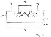
- FIG. 1is a simplified diagram of an FET showing the self-heating. Shown in FIG. 1 are channel 101 , gate 102 , oxide 103 and substrate 104 . Within the channel 101 to gate 102 junction, the self-heating is shown as bursts 105 . Points where the source voltage Vs, the drain voltage Vd, and the gate voltage Vg are also shown. As the voltages are applied to the source, gate and drain of the device, internal heating begins to occur. As shown in this simplified diagram, the self-heating bursts 105 are non-uniform and in their distribution and degree.
- FIG. 2is a schematic diagram illustrating a single finger VLSI circuit. Shown in FIG. 2 is a single finger VLSI 201 .
- P junction FET (PFET) 202 and N junction FET (NFET) 203comprise the VLSI 201 shown in FIG. 2 .
- PFET 202is comprised of a source 202 a , a drain 202 b , and a gate 202 c
- NFET 203is comprised of a source 203 a , a drain 203 b , and a gate 203 c .
- Voltage (+V) 205 and Ground (GND) 206are also depicted in FIG. 2 .
- PFET 202 and NFET 203are controlled through gate connector 204 .
- the gates and gate connectorare shown in a hatched detail.
- the gate connector 204extends horizontally between gates 202 c and 203 c .
- the “single finger” structure of the VLSI 201refers to the single vertical part of the gate 204 .
- the regions about the PFET 202 and the NFET 203will begin to generate heat due to the flow of current through each of the PFET 202 and NFET 203 . As stated earlier, this heat, if allowed to reach critical values, can deteriorate ideal operation or completely destroy the VLSI 201 .
- Polysiliconor polycrystalline silicon, has long been used as the conducting gate and gate connector material in MOSFET and CMOS processing technologies. For these technologies it is deposited using reactors at high temperatures. More recently, polysilicon is being used in very large scale integration (VLSI) electronics. The main advantage of polysilicon is that it allows more complex, high-speed circuitry to be created on the glass substrate.
- VLSIvery large scale integration
- FIG. 3is a schematic diagram illustrating a multi-finger VLSI circuit. Shown in FIG. 3 is a multi-finger VLSI 301 .
- a plurality of P junction FETs (PFETs) 302 and a plurality of N junction FETs (NFETs) 303comprise the VLSI 301 shown in FIG. 3 .
- Each PFET 302is comprised of a source 302 a , a drain 302 b , and a gate 302 c
- each NFET 303is comprised of a source 303 a , a drain 303 b , and a gate 303 c .
- Voltage (+V) 305 and Ground (GND) 306are also depicted in FIG. 3 .
- Each PFET 302 and each NFET 303are controlled through gate connector 304 .
- the gates and gate connectorsare shown in a hatched detail.
- the gate connector 304extends horizontally between each of the FETs.
- Vout 307is the output voltage points for the FETs.
- the “multi-finger” structure of the VLSI 301refers to the plurality of 302 c gates and plurality of 303 c gates.
- the regions about the PFETs 302 and the NFET 303will begin to generate heat due to the flow of current through each of the PFETs 302 and NFETs 303 .
- this heatif allowed to reach critical values, can deteriorate ideal operation or completely destroy the VLSI 301 .
- the Berkeley Short-channel IGFET Model for MOS transistors(BSIM).
- the BSIM and other design modelsapproximate the internal operations of a circuit at a design stage. These models use know values and operating parameters of the circuit components to assist in the design of the final integrated circuit using highly mathematical statistical models.
- the BSIMin particular also includes statistical models to estimate the internal heating of the integrated circuit. Although the BSIM is a good method to approximate the internal temperature of the integrated circuit, using approximations and statistical models can only produce estimated results.
- the self-heatingis also know to be non-uniform throughout the topology of the circuit. Again, only approximations and estimations are available to measure the differences in temperature occurring at these differing levels of the integrated circuit. As a result, the integrated circuits that are designed using the conventional methods cannot accurately account for the variations in temperature throughout the cross sections of the final integrated circuit product.
- An object of the present inventionis to substantially solve at least the above problems and/or disadvantages and to provide at least the advantages below.
- an object of the present inventionis to provide a system for measuring internal temperatures of high-powered VLSI circuits.
- Another object of the present inventionis to provide a system to assist in the design of integrated circuits independent of the conventional self-heating models.
- Another object of the present inventionis to provide a system to identify circuit topologies prone to self-heating.
- a further object of the present inventionis to provide a system to improve thermal model-to-hardware correlation.
- It is still a further object of the present inventionis to provide a system for assessing thermal impact on an integrated circuit device performance.
- a temperature sensor for an integrated circuit having at least one field effect transistor (FET) having a polysilicon gatecomprising means for supplying a current and a voltage to the polysilicon gate; and means for monitoring changes in the current and the voltage of the polysilicon gate, wherein the polysilicon gate of the at least one FET is electrically isolated from other components of the integrated circuit, and wherein the changes in the current or voltage are used to calculate a change in resistance of the polysilicon gate, and wherein the change in resistance of the polysilicon gate is used to calculate a temperature change within the integrated circuit.
- FETfield effect transistor
- Another object of the present inventionis to embed a thermometer within on-chip clock buffers, I/O drivers, wordline drivers, latches, etc.
- FIG. 1is a simplified diagram of an FET showing the self-heating
- FIG. 2is a schematic diagram illustrating a single finger VLSI circuit
- FIG. 3is a schematic diagram illustrating a multi-finger VLSI circuit
- FIG. 4is a schematic diagram of a multi-finger VLSI circuit according to an embodiment of the present invention.
- FIG. 5is a chart illustrating the effect of multiple active fingers
- FIG. 6is a graph illustrating the die-to-die variation when only the sensor is active
- FIG. 7is a graph illustrating the thermal resistance of a NFET versus a PFET
- FIG. 8illustrates four different thermal resistances versus conductivity graphs
- FIG. 9is a graph illustrating performance versus temperature of a clock buffer
- FIG. 10is a graph illustrating performance versus temperature
- FIG. 11is a diagram illustrating an integrated circuit configuration for determining the temperature at sub-threshold operating conditions according to additional embodiments of the present invention.
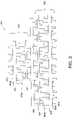
- FIG. 4is a schematic diagram of a multi-finger VLSI circuit according to an embodiment of the present invention. Shown in FIG. 4 is a multi-finger VLSI 401 .
- a plurality of P junction FETs (PFETs) 402 and a plurality of N junction FETs (NFETs) 403comprise the VLSI 401 shown in FIG. 4 .
- Each PFET 402is comprised of a source 402 a , a drain 402 b , and a gate 402 c .
- Each NFET 403is comprised of a source 403 a , a drain 403 b , and a gate 403 c .
- Voltage (+V) 405 and Ground (GND) 406are also depicted in FIG. 4 .
- Each gate of each PFET 402 and each NFET 403are controlled through gate connector 404 .
- the gates and gate connectorare shown in a hatched detail.
- the gate connector 404connects to each gate of the PFETs 402 and NFETs 403 , and extends horizontally between them.
- Vout 407is the output voltage points for the FETs. Additionally shown in FIG.
- PFET 420comprised of a source 420 a , a drain 420 b , and a gate 420 c
- NFET 430comprised of a source 430 a , a drain 430 b , and a gate 430 c.
- each of gate 420 c and gate 430 chas been isolated from the gate connector 404 . Also each end of gates 420 c and 430 c has been extended by gate extenders 443 , 444 , 453 and 454 . Connected to gate extender 444 is a probe point 441 , and connected to gate extender 443 is a probe point 442 . Connected to gate extender 454 is a probe point 451 , and connected to gate extender 453 is a probe point 452 .
- Gate 420 c and gate extenders 443 and 444comprise temperature sensor 440 .
- Gate 430 c and gate extenders 453 and 454comprise temperature sensor 450 .
- PFET 420 and NFET 430become inactive when their respective gates 420 c and 430 c are utilized as temperature sensors. This loss of a single PFET and a single NFET in the VLSI 401 produces a minimal impact on the operation of the VLSI 401 , but greatly increases the use of the gates for the temperature sensors.
- temperature sensor 440The operation of a temperature sensor according to the present invention will now be described with reference to FIG. 4 .
- the following description of the present inventionwill be limited to temperature sensor 440 , although the description also applies to temperature sensor 450 .
- the probe points 441 and 442provide access points to the temperature sensor 440 to supply a voltage and a current through the gate 420 c of the temperature sensor 440 , and measure the voltage across the temperature sensor 440 , and measure the current through the temperature sensor 440 .
- the resistance of the temperature sensor 440is calculated by the following Equation 3
- RV I ( 3 ) where R is the calculated resistance, V is the measured voltage, and I is the measured current.
- the resistance of the temperature sensor 440can be calibrated as a function of the chuck temperature.
- the resistance of the temperature sensor 440can be calibrated as a function of the sub-threshold leakages. Whichever method is utilized, and other calibration techniques are of course contemplated, a calibration of the temperature sensor is needed to ensure proper temperature measurements.
- mode 1all gates active (i.e. all of the gates and the temperature sensor (i.e. the gates 420 c and 430 c of the temperature sensors 440 and 450 , respectively) are active); mode 2—only the temperature sensor is active; mode 3—all gates are active and the temperature sensor is inactive; and mode 4—all gates inactive (all gates and the temperature sensor are inactive).
- the temperature sensor gateis considered inactive when no current or voltage is introduced through its gate element.
- Mode 1determines the temperature of the integrated circuit while all of the gates of all of the PFETs and NFETs are active, and the temperature sensor is active. This first mode of all gates active determines the highest level of internal heating that will occur in the integrated circuit.
- Mode 2determines the internal heat generated while only the temperature sensor gate is active, and can be used as a calibration temperature.
- Mode 3measures the current and voltage of the temperature sensor while all of the other gates are active, but no current and voltage is being applied to the temperature sensor. This mode allows for any leakage currents and voltages to be measured, and can be used in calibration procedures.
- Mode 4measures the current and voltage of the temperature sensor while all of the gates are inactive, including the temperature sensor gate.
- temperature measurements attained through the determination of sub-threshold leakage currentscan also be obtained using the temperature sensor according to the embodiment of the present invention.
- the leakages through these devicescan be measured using a similar four pad temperature sensor structure as previously described.
- II 0 ( e (Vq/kT) ⁇ 1) (4)
- Vthe applied voltage
- Tthe temperature
- qthe electron charge
- I 0the saturation current.
- the current-voltage characteristicscan be obtained for the leakages and the temperature can be extrapolated from the obtained leakage characteristics especially from the sub-threshold leakages.
- FIG. 11is a diagram illustrating an integrated circuit configuration for determining the temperature at sub-threshold operating conditions according to additional embodiments of the present invention. Many of the elements shown in FIG. 11 are similar to those in FIG. 4 , and as such, the duplicative elements will not be described herein.
- Integrated circuit 1101is shown in FIG. 11 .
- two additional embodimentsare shown in FIG. 11 ; a second embodiment for determining the sub-threshold leakage current between the sources and the drains of the FETs of the integrated circuit, and a third embodiment for determining the sub-threshold leakage current between a single source and a single drain of one FET of the integrated circuit.
- intermediate variationsare contemplated, namely, the leakage current of any number of the FETs, from one to all, can be determined using this method.
- the temperaturecan then be determined from the slope of the plot of the Vq/kT term.
- the new elements of the second embodimentinclude current pad 1102 and current pad 1103 .
- the FETsBy placing the FETs into a sub-threshold state by applying the proper voltages to Voltage 405 and Vout 40 , the sub-threshold leakage current between the sources and the drains can be measured at pads 1102 and 1103 . Then the temperature can be determined by calculating the slope of the line formed by the plot of Vq/kT.
- the third embodiment PFET 1110is shown comprising source 1110 a , drain 1110 b , and gate 1110 c .
- PFET 1100has been electrically isolated from Voltage 405 and Vout 407 .
- pad 1104Connected to source 1110 a is pad 1104
- drain 1110 bis pad 1105 .
- the leakage current of the single PFET 1110can be determined by placing the PFET 1110 into a sub-threshold state by applying the proper voltages to pads 1104 and 1105 , the sub-threshold leakage current between the source 1110 a and the drain 1110 b can be measured at pads 1104 and 1105 . Then the temperature can be determined by calculating the slope of the line formed by the plot of Vq/kT.
- FIG. 5is a chart illustrating the effect of multiple active fingers. Shown in FIG. 5 are the junction and layer M 1 temperature rises. As can be seen, an increase in the active number of fingers increases the junction temperature. Also, a close thermal coupling between the fingers within the same body increases the thermal resistance by three times.
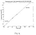
- FIG. 6is a graph illustrating the die-to-die variation when only the sensor is active. As the power increases, the temperature change increases almost linearly.
- the following tablesillustrate thermal resistance data as determined according to the present invention.
- the temperature sensorsare located at two different FET locations, and listed in the tables as “1”or “2”.
- the conditions of the deviceare as follows: “A” denotes that only the sensor gate is active during temperature measurements; “B” denotes that all of the gates are active during temperature measurements; and “C” denotes that all of the gates except for the sensor gate are active during temperature measurements.
- FIG. 7is a graph illustrating the thermal resistance of a NFET versus a PFET. During the temperature measurements, only the sensor gate was active. Also, the gate, the source and the drain voltages were all equal.
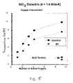
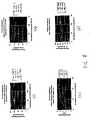
- FIG. 8illustrates four different thermal resistances versus conductivity graphs.
- Diagram (a) of FIG. 8illustrates the thermal resistance based on the temperature of the sensor versus standard test data of 0.13 micron technology.
- Diagram (b) of FIG. 8illustrates the thermal resistance based on the temperature of the sensor versus standard test data of 0.09 micron technology.
- Diagram (c) of FIG. 8illustrates the thermal resistance ratios of the temperature of the sensors in an all on versus only the sensor on of 0.13 micron technology.
- Diagram (d) of FIG. 8illustrates the thermal resistance of maximum versus sensor readings of 0.13 micron technology.
- FIG. 9is a graph illustrating performance versus temperature of a clock buffer. The graph is shown scaled to a bilk performance at 25 degrees Celsius. The performance gain of the SOI is 20% greater than the bulk. The performance change is 1.2% per 10 degrees Celsius for the SOI, and 1.32% per 10 degrees Celsius for the bulk.
- FIG. 10is a graph illustrating performance versus temperature. As can be seen the delay increases as the temperature increases of the two technologies shown in FIG. 10 .
- Similar methodologythat is a four point probe structure at the end of metal lines wherein the two top pads are used for voltage and current and the two bottom pads are used for voltage and current, can be used for measuring the temperature of metal lines by calibrating the resistance of the metal lines connected to a device or a circuit.
- individual devicescan be separated in the multifinger topology and source and drain current can be separately tapped off in the sub-threshold regime.
- the spacing of the devicescan also be varied to study the temperature rise based on the leakage data based on various spacing designs.
- both of the structurescan be used in planar or in 3-D plane topology.
- the present inventionprovides a system for measuring internal temperatures of high-powered VLSI circuits, can vitally assist in the design of integrated circuits independent of the conventional self-heating models, is able to identify circuit topologies prone to self-heating, can improve thermal model-to-hardware correlation, enables the assessing thermal impact on an integrated circuit device performance, can greatly assist in the design of integrated circuits independent of the conventional self-heating models, and can greatly improve the thermal model-to-hardware correlation.
Landscapes
- Engineering & Computer Science (AREA)
- Manufacturing & Machinery (AREA)
- Automation & Control Theory (AREA)
- Computer Hardware Design (AREA)
- Microelectronics & Electronic Packaging (AREA)
- Power Engineering (AREA)
- Semiconductor Integrated Circuits (AREA)
Abstract
Description
∇λ∇T+q=0 (1)
where T is the temperature, q is the heat/volume, and λis the thermal conductivity, can be used to analyze and determine the temperature change. By determining the thermal conductivity of the isolated gate finger, i.e.
where R is the calculated resistance, V is the measured voltage, and I is the measured current.
I=I0(e(Vq/kT)−1) (4)
where V is the applied voltage, T is the temperature, q is the electron charge, and I0is the saturation current. The current-voltage characteristics can be obtained for the leakages and the temperature can be extrapolated from the obtained leakage characteristics especially from the sub-threshold leakages.
| TABLE 1 | ||||
| 0.13 micron | 0.09 micron | |||
| Gate | technology | technology | 0.09 | 0.09 |
| Conditions | (degrees C/mW) | (degrees C/mW) | micron | micron |
| 1A | 18.5 | 24.2 | ||
| 1B | 4.9 | 5.8 | ||
| 1C | 2.6 | 2.6 | ||
| 2A | 16.1 | 22.6 | 39 | 41 |
| 2B | 2.0 | 1.8 | 4.4 | 4.7 |
| 2C | 1.1 | 0.9 | 3.2 | |
| TABLE 2 | ||
| 0.13 micron | 0.09 micron | |
| Gate | technology (degrees | technology (degrees |
| Conditions | C-micrometer/mW) | C-micrometer/mW) |
| 1A | 49.40 | 64.61 |
| 1B | 104.66 | 123.89 |
| 1C | 48.59 | 48.59 |
| 2A | 42.99 | 60.34 |
| 2B | 149.52 | 134.57 |
| 2C | 79.30 | 64.88 |
Claims (22)
I=I0(e(Vq/kT)−1)
I=I0(e(Vq/kT)−1)
Priority Applications (1)
| Application Number | Priority Date | Filing Date | Title |
|---|---|---|---|
| US10/899,768US7176508B2 (en) | 2004-07-27 | 2004-07-27 | Temperature sensor for high power very large scale integration circuits |
Applications Claiming Priority (1)
| Application Number | Priority Date | Filing Date | Title |
|---|---|---|---|
| US10/899,768US7176508B2 (en) | 2004-07-27 | 2004-07-27 | Temperature sensor for high power very large scale integration circuits |
Publications (2)
| Publication Number | Publication Date |
|---|---|
| US20060024852A1 US20060024852A1 (en) | 2006-02-02 |
| US7176508B2true US7176508B2 (en) | 2007-02-13 |
Family
ID=35732813
Family Applications (1)
| Application Number | Title | Priority Date | Filing Date |
|---|---|---|---|
| US10/899,768Expired - LifetimeUS7176508B2 (en) | 2004-07-27 | 2004-07-27 | Temperature sensor for high power very large scale integration circuits |
Country Status (1)
| Country | Link |
|---|---|
| US (1) | US7176508B2 (en) |
Cited By (28)
| Publication number | Priority date | Publication date | Assignee | Title |
|---|---|---|---|---|
| US20060047474A1 (en)* | 2004-09-02 | 2006-03-02 | International Business Machines Corporation | SELF HEATING MONITOR FOR SiGe AND SOI CMOS DEVICES |
| US20080222587A1 (en)* | 2007-03-05 | 2008-09-11 | Tela Innovations, Inc. | Integrated Circuit Cell Library for Multiple Patterning |
| DE102008023215A1 (en)* | 2008-05-19 | 2009-12-03 | Friedrich-Alexander-Universität Erlangen-Nürnberg | Method for operating temperature control of a MOS-controlled semiconductor power device and device for carrying out the method |
| US20100153954A1 (en)* | 2008-12-11 | 2010-06-17 | Qualcomm Incorporated | Apparatus and Methods for Adaptive Thread Scheduling on Asymmetric Multiprocessor |
| US20100187634A1 (en)* | 2008-03-13 | 2010-07-29 | Tela Innovations, Inc. | Channelized Gate Level Cross-Coupled Transistor Device with Cross-Coupled Transistors Defined on Four Gate Electrode Tracks with Crossing Gate Electrode Connections |
| US20110161909A1 (en)* | 2007-08-02 | 2011-06-30 | Tela Innovations, Inc. | Methods for Designing Semiconductor Device with Dynamic Array Section |
| US8541879B2 (en) | 2007-12-13 | 2013-09-24 | Tela Innovations, Inc. | Super-self-aligned contacts and method for making the same |
| US8549462B2 (en) | 2011-08-23 | 2013-10-01 | International Business Machines Corporation | Thermal coupling determination and representation |
| US8549455B2 (en) | 2007-08-02 | 2013-10-01 | Tela Innovations, Inc. | Methods for cell phasing and placement in dynamic array architecture and implementation of the same |
| US8653857B2 (en) | 2006-03-09 | 2014-02-18 | Tela Innovations, Inc. | Circuitry and layouts for XOR and XNOR logic |
| US8658542B2 (en) | 2006-03-09 | 2014-02-25 | Tela Innovations, Inc. | Coarse grid design methods and structures |
| US8661392B2 (en) | 2009-10-13 | 2014-02-25 | Tela Innovations, Inc. | Methods for cell boundary encroachment and layouts implementing the Same |
| US8680626B2 (en) | 2007-10-26 | 2014-03-25 | Tela Innovations, Inc. | Methods, structures, and designs for self-aligning local interconnects used in integrated circuits |
| US8701071B2 (en) | 2008-01-31 | 2014-04-15 | Tela Innovations, Inc. | Enforcement of semiconductor structure regularity for localized transistors and interconnect |
| US8759985B2 (en) | 2008-03-27 | 2014-06-24 | Tela Innovations, Inc. | Methods for multi-wire routing and apparatus implementing same |
| US8823062B2 (en) | 2006-03-09 | 2014-09-02 | Tela Innovations, Inc. | Integrated circuit with offset line end spacings in linear gate electrode level |
| US8839175B2 (en) | 2006-03-09 | 2014-09-16 | Tela Innovations, Inc. | Scalable meta-data objects |
| US8863063B2 (en) | 2009-05-06 | 2014-10-14 | Tela Innovations, Inc. | Finfet transistor circuit |
| US20150035568A1 (en)* | 2013-08-01 | 2015-02-05 | Taiwan Semiconductor Manufacturing Company Ltd. | Temperature detector and controlling heat |
| US9035359B2 (en) | 2006-03-09 | 2015-05-19 | Tela Innovations, Inc. | Semiconductor chip including region including linear-shaped conductive structures forming gate electrodes and having electrical connection areas arranged relative to inner region between transistors of different types and associated methods |
| US9122832B2 (en) | 2008-08-01 | 2015-09-01 | Tela Innovations, Inc. | Methods for controlling microloading variation in semiconductor wafer layout and fabrication |
| US9159627B2 (en) | 2010-11-12 | 2015-10-13 | Tela Innovations, Inc. | Methods for linewidth modification and apparatus implementing the same |
| US9170165B2 (en) | 2013-03-25 | 2015-10-27 | Globalfoundries U.S. 2 Llc | Workfunction modulation-based sensor to measure pressure and temperature |
| US9230910B2 (en) | 2006-03-09 | 2016-01-05 | Tela Innovations, Inc. | Oversized contacts and vias in layout defined by linearly constrained topology |
| US9563733B2 (en) | 2009-05-06 | 2017-02-07 | Tela Innovations, Inc. | Cell circuit and layout with linear finfet structures |
| US9754878B2 (en) | 2006-03-09 | 2017-09-05 | Tela Innovations, Inc. | Semiconductor chip including a chip level based on a layout that includes both regular and irregular wires |
| US9970981B2 (en)* | 2016-08-02 | 2018-05-15 | Semiconductor Manufacturing International (Shanghai) Corporation | Method and device for temperature measurement of FinFET devices |
| US10948359B2 (en) | 2018-10-30 | 2021-03-16 | Analog Devices International Unlimited Company | Techniques for junction temperature determination of power switches |
Families Citing this family (4)
| Publication number | Priority date | Publication date | Assignee | Title |
|---|---|---|---|---|
| US7805274B2 (en)* | 2006-11-13 | 2010-09-28 | International Business Machines Corporation | Structure and methodology for characterizing device self-heating |
| US7798703B2 (en)* | 2007-05-09 | 2010-09-21 | Infineon Technologies Ag | Apparatus and method for measuring local surface temperature of semiconductor device |
| US9501918B2 (en)* | 2011-08-24 | 2016-11-22 | Safetyminded Holdings, Inc. | Human safety indicator |
| JP6971199B2 (en)* | 2018-05-31 | 2021-11-24 | 東京エレクトロン株式会社 | Board processing method and board processing equipment |
Citations (8)
| Publication number | Priority date | Publication date | Assignee | Title |
|---|---|---|---|---|
| US5683569A (en)* | 1996-02-28 | 1997-11-04 | Motorola, Inc. | Method of sensing a chemical and sensor therefor |
| US6252277B1 (en) | 1999-09-09 | 2001-06-26 | Chartered Semiconductor Manufacturing Ltd. | Embedded polysilicon gate MOSFET |
| US6261935B1 (en) | 1999-12-13 | 2001-07-17 | Chartered Semiconductor Manufacturing Ltd. | Method of forming contact to polysilicon gate for MOS devices |
| US6456104B1 (en)* | 1999-08-18 | 2002-09-24 | International Business Machines Corporation | Method and structure for in-line monitoring of negative bias temperature instability in field effect transistors |
| US20030076153A1 (en)* | 2001-10-17 | 2003-04-24 | Kaveh Shakeri | Controlling circuit power consumption through body voltage control |
| US6573169B2 (en) | 1998-02-27 | 2003-06-03 | Micron Technology, Inc. | Highly conductive composite polysilicon gate for CMOS integrated circuits |
| US20040042529A1 (en)* | 2002-08-30 | 2004-03-04 | International Business Machines Corporation | Device for sensing temperature of an electronic chip |
| US6774713B2 (en)* | 2002-07-30 | 2004-08-10 | Renesas Technology Corp. | Circuit for producing a reference voltage for transistors set to a standby state |
- 2004
- 2004-07-27USUS10/899,768patent/US7176508B2/ennot_activeExpired - Lifetime
Patent Citations (8)
| Publication number | Priority date | Publication date | Assignee | Title |
|---|---|---|---|---|
| US5683569A (en)* | 1996-02-28 | 1997-11-04 | Motorola, Inc. | Method of sensing a chemical and sensor therefor |
| US6573169B2 (en) | 1998-02-27 | 2003-06-03 | Micron Technology, Inc. | Highly conductive composite polysilicon gate for CMOS integrated circuits |
| US6456104B1 (en)* | 1999-08-18 | 2002-09-24 | International Business Machines Corporation | Method and structure for in-line monitoring of negative bias temperature instability in field effect transistors |
| US6252277B1 (en) | 1999-09-09 | 2001-06-26 | Chartered Semiconductor Manufacturing Ltd. | Embedded polysilicon gate MOSFET |
| US6261935B1 (en) | 1999-12-13 | 2001-07-17 | Chartered Semiconductor Manufacturing Ltd. | Method of forming contact to polysilicon gate for MOS devices |
| US20030076153A1 (en)* | 2001-10-17 | 2003-04-24 | Kaveh Shakeri | Controlling circuit power consumption through body voltage control |
| US6774713B2 (en)* | 2002-07-30 | 2004-08-10 | Renesas Technology Corp. | Circuit for producing a reference voltage for transistors set to a standby state |
| US20040042529A1 (en)* | 2002-08-30 | 2004-03-04 | International Business Machines Corporation | Device for sensing temperature of an electronic chip |
Cited By (130)
| Publication number | Priority date | Publication date | Assignee | Title |
|---|---|---|---|---|
| US7862233B2 (en)* | 2004-09-02 | 2011-01-04 | International Business Machines Corporation | Self heating monitor for SiGe and SOI CMOS devices |
| US20070262359A1 (en)* | 2004-09-02 | 2007-11-15 | International Business Machines Corporation | SELF HEATING MONITOR FOR SiGe AND SOI CMOS DEVICES |
| US7406397B2 (en)* | 2004-09-02 | 2008-07-29 | International Business Machines Corporation | Self heating monitor for SiGe and SOI CMOS devices |
| US20060047474A1 (en)* | 2004-09-02 | 2006-03-02 | International Business Machines Corporation | SELF HEATING MONITOR FOR SiGe AND SOI CMOS DEVICES |
| US8412487B2 (en)* | 2004-09-02 | 2013-04-02 | International Business Machines Corporation | Self heating monitor for SiGe and SOI CMOS devices |
| US20110029274A1 (en)* | 2004-09-02 | 2011-02-03 | International Business Machines Corporation | SELF HEATING MONITOR FOR SiGe AND SOI CMOS DEVICES |
| US9240413B2 (en) | 2006-03-09 | 2016-01-19 | Tela Innovations, Inc. | Methods, structures, and designs for self-aligning local interconnects used in integrated circuits |
| US8952425B2 (en) | 2006-03-09 | 2015-02-10 | Tela Innovations, Inc. | Integrated circuit including at least four linear-shaped conductive structures having extending portions of different length |
| US10186523B2 (en) | 2006-03-09 | 2019-01-22 | Tela Innovations, Inc. | Semiconductor chip having region including gate electrode features formed in part from rectangular layout shapes on gate horizontal grid and first-metal structures formed in part from rectangular layout shapes on at least eight first-metal gridlines of first-metal vertical grid |
| US10141335B2 (en) | 2006-03-09 | 2018-11-27 | Tela Innovations, Inc. | Semiconductor CIP including region having rectangular-shaped gate structures and first metal structures |
| US10141334B2 (en) | 2006-03-09 | 2018-11-27 | Tela Innovations, Inc. | Semiconductor chip including region having rectangular-shaped gate structures and first-metal structures |
| US8839175B2 (en) | 2006-03-09 | 2014-09-16 | Tela Innovations, Inc. | Scalable meta-data objects |
| US9917056B2 (en) | 2006-03-09 | 2018-03-13 | Tela Innovations, Inc. | Coarse grid design methods and structures |
| US8921897B2 (en) | 2006-03-09 | 2014-12-30 | Tela Innovations, Inc. | Integrated circuit with gate electrode conductive structures having offset ends |
| US9905576B2 (en) | 2006-03-09 | 2018-02-27 | Tela Innovations, Inc. | Semiconductor chip including region having rectangular-shaped gate structures and first metal structures |
| US10230377B2 (en) | 2006-03-09 | 2019-03-12 | Tela Innovations, Inc. | Circuitry and layouts for XOR and XNOR logic |
| US8921896B2 (en) | 2006-03-09 | 2014-12-30 | Tela Innovations, Inc. | Integrated circuit including linear gate electrode structures having different extension distances beyond contact |
| US8823062B2 (en) | 2006-03-09 | 2014-09-02 | Tela Innovations, Inc. | Integrated circuit with offset line end spacings in linear gate electrode level |
| US8653857B2 (en) | 2006-03-09 | 2014-02-18 | Tela Innovations, Inc. | Circuitry and layouts for XOR and XNOR logic |
| US8946781B2 (en) | 2006-03-09 | 2015-02-03 | Tela Innovations, Inc. | Integrated circuit including gate electrode conductive structures with different extension distances beyond contact |
| US9859277B2 (en) | 2006-03-09 | 2018-01-02 | Tela Innovations, Inc. | Methods, structures, and designs for self-aligning local interconnects used in integrated circuits |
| US9425145B2 (en) | 2006-03-09 | 2016-08-23 | Tela Innovations, Inc. | Oversized contacts and vias in layout defined by linearly constrained topology |
| US9443947B2 (en) | 2006-03-09 | 2016-09-13 | Tela Innovations, Inc. | Semiconductor chip including region having integrated circuit transistor gate electrodes formed by various conductive structures of specified shape and position and method for manufacturing the same |
| US9754878B2 (en) | 2006-03-09 | 2017-09-05 | Tela Innovations, Inc. | Semiconductor chip including a chip level based on a layout that includes both regular and irregular wires |
| US9741719B2 (en) | 2006-03-09 | 2017-08-22 | Tela Innovations, Inc. | Methods, structures, and designs for self-aligning local interconnects used in integrated circuits |
| US9711495B2 (en) | 2006-03-09 | 2017-07-18 | Tela Innovations, Inc. | Oversized contacts and vias in layout defined by linearly constrained topology |
| US9673825B2 (en) | 2006-03-09 | 2017-06-06 | Tela Innovations, Inc. | Circuitry and layouts for XOR and XNOR logic |
| US9009641B2 (en) | 2006-03-09 | 2015-04-14 | Tela Innovations, Inc. | Circuits with linear finfet structures |
| US9035359B2 (en) | 2006-03-09 | 2015-05-19 | Tela Innovations, Inc. | Semiconductor chip including region including linear-shaped conductive structures forming gate electrodes and having electrical connection areas arranged relative to inner region between transistors of different types and associated methods |
| US9589091B2 (en) | 2006-03-09 | 2017-03-07 | Tela Innovations, Inc. | Scalable meta-data objects |
| US10217763B2 (en) | 2006-03-09 | 2019-02-26 | Tela Innovations, Inc. | Semiconductor chip having region including gate electrode features of rectangular shape on gate horizontal grid and first-metal structures of rectangular shape on at least eight first-metal gridlines of first-metal vertical grid |
| US9230910B2 (en) | 2006-03-09 | 2016-01-05 | Tela Innovations, Inc. | Oversized contacts and vias in layout defined by linearly constrained topology |
| US9336344B2 (en) | 2006-03-09 | 2016-05-10 | Tela Innovations, Inc. | Coarse grid design methods and structures |
| US8658542B2 (en) | 2006-03-09 | 2014-02-25 | Tela Innovations, Inc. | Coarse grid design methods and structures |
| US9425273B2 (en) | 2006-03-09 | 2016-08-23 | Tela Innovations, Inc. | Semiconductor chip including integrated circuit including at least five gate level conductive structures having particular spatial and electrical relationship and method for manufacturing the same |
| US9425272B2 (en) | 2006-03-09 | 2016-08-23 | Tela Innovations, Inc. | Semiconductor chip including integrated circuit including four transistors of first transistor type and four transistors of second transistor type with electrical connections between various transistors and methods for manufacturing the same |
| US20080222587A1 (en)* | 2007-03-05 | 2008-09-11 | Tela Innovations, Inc. | Integrated Circuit Cell Library for Multiple Patterning |
| US10074640B2 (en) | 2007-03-05 | 2018-09-11 | Tela Innovations, Inc. | Integrated circuit cell library for multiple patterning |
| US8667443B2 (en) | 2007-03-05 | 2014-03-04 | Tela Innovations, Inc. | Integrated circuit cell library for multiple patterning |
| US9633987B2 (en) | 2007-03-05 | 2017-04-25 | Tela Innovations, Inc. | Integrated circuit cell library for multiple patterning |
| US9595515B2 (en) | 2007-03-07 | 2017-03-14 | Tela Innovations, Inc. | Semiconductor chip including integrated circuit defined within dynamic array section |
| US9424387B2 (en) | 2007-03-07 | 2016-08-23 | Tela Innovations, Inc. | Methods for cell phasing and placement in dynamic array architecture and implementation of the same |
| US9910950B2 (en) | 2007-03-07 | 2018-03-06 | Tela Innovations, Inc. | Methods for cell phasing and placement in dynamic array architecture and implementation of the same |
| US8966424B2 (en) | 2007-03-07 | 2015-02-24 | Tela Innovations, Inc. | Methods for cell phasing and placement in dynamic array architecture and implementation of the same |
| US8549455B2 (en) | 2007-08-02 | 2013-10-01 | Tela Innovations, Inc. | Methods for cell phasing and placement in dynamic array architecture and implementation of the same |
| US8759882B2 (en) | 2007-08-02 | 2014-06-24 | Tela Innovations, Inc. | Semiconductor device with dynamic array sections defined and placed according to manufacturing assurance halos |
| US8756551B2 (en) | 2007-08-02 | 2014-06-17 | Tela Innovations, Inc. | Methods for designing semiconductor device with dynamic array section |
| US20110161909A1 (en)* | 2007-08-02 | 2011-06-30 | Tela Innovations, Inc. | Methods for Designing Semiconductor Device with Dynamic Array Section |
| US10734383B2 (en) | 2007-10-26 | 2020-08-04 | Tela Innovations, Inc. | Methods, structures, and designs for self-aligning local interconnects used in integrated circuits |
| US8680626B2 (en) | 2007-10-26 | 2014-03-25 | Tela Innovations, Inc. | Methods, structures, and designs for self-aligning local interconnects used in integrated circuits |
| US8951916B2 (en) | 2007-12-13 | 2015-02-10 | Tela Innovations, Inc. | Super-self-aligned contacts and method for making the same |
| US9281371B2 (en) | 2007-12-13 | 2016-03-08 | Tela Innovations, Inc. | Super-self-aligned contacts and method for making the same |
| US8541879B2 (en) | 2007-12-13 | 2013-09-24 | Tela Innovations, Inc. | Super-self-aligned contacts and method for making the same |
| US9818747B2 (en) | 2007-12-13 | 2017-11-14 | Tela Innovations, Inc. | Super-self-aligned contacts and method for making the same |
| US10461081B2 (en) | 2007-12-13 | 2019-10-29 | Tel Innovations, Inc. | Super-self-aligned contacts and method for making the same |
| US9202779B2 (en) | 2008-01-31 | 2015-12-01 | Tela Innovations, Inc. | Enforcement of semiconductor structure regularity for localized transistors and interconnect |
| US8701071B2 (en) | 2008-01-31 | 2014-04-15 | Tela Innovations, Inc. | Enforcement of semiconductor structure regularity for localized transistors and interconnect |
| US9530734B2 (en) | 2008-01-31 | 2016-12-27 | Tela Innovations, Inc. | Enforcement of semiconductor structure regularity for localized transistors and interconnect |
| US8866197B2 (en) | 2008-03-13 | 2014-10-21 | Tela Innovations, Inc. | Integrated circuit including cross-coupled transistors having gate electrodes formed within gate level feature layout channels with at least two gate electrodes electrically connected to each other through another transistor forming gate level feature |
| US8592872B2 (en) | 2008-03-13 | 2013-11-26 | Tela Innovations, Inc. | Integrated circuit including cross-coupled transistors with two transistors of different type having gate electrodes formed by common gate level feature with shared diffusion regions on opposite sides of common gate level feature |
| US8853794B2 (en) | 2008-03-13 | 2014-10-07 | Tela Innovations, Inc. | Integrated circuit within semiconductor chip including cross-coupled transistor configuration |
| US8853793B2 (en) | 2008-03-13 | 2014-10-07 | Tela Innovations, Inc. | Integrated circuit including gate electrode level region including cross-coupled transistors having gate contacts located over inner portion of gate electrode level region and offset gate level feature line ends |
| US10727252B2 (en) | 2008-03-13 | 2020-07-28 | Tela Innovations, Inc. | Semiconductor chip including integrated circuit having cross-coupled transistor configuration and method for manufacturing the same |
| US8847329B2 (en) | 2008-03-13 | 2014-09-30 | Tela Innovations, Inc. | Cross-coupled transistor circuit defined having diffusion regions of common node on opposing sides of same gate electrode track with at least two non-inner positioned gate contacts |
| US8872283B2 (en) | 2008-03-13 | 2014-10-28 | Tela Innovations, Inc. | Integrated circuit including cross-coupled transistors having gate electrodes formed within gate level feature layout channels with shared diffusion regions on opposite sides of two-transistor-forming gate level feature |
| US8835989B2 (en) | 2008-03-13 | 2014-09-16 | Tela Innovations, Inc. | Integrated circuit including cross-coupled transistors having gate electrodes formed within gate level feature layout channels with gate electrode placement specifications |
| US8836045B2 (en) | 2008-03-13 | 2014-09-16 | Tela Innovations, Inc. | Cross-coupled transistor circuit having diffusion regions of common node on opposing sides of same gate electrode track |
| US8816402B2 (en) | 2008-03-13 | 2014-08-26 | Tela Innovations, Inc. | Integrated circuit including cross-coupled transistors having gate electrodes formed within gate level feature layout channels with gate level feature layout channel including single transistor |
| US10658385B2 (en) | 2008-03-13 | 2020-05-19 | Tela Innovations, Inc. | Cross-coupled transistor circuit defined on four gate electrode tracks |
| US8785978B2 (en) | 2008-03-13 | 2014-07-22 | Tela Innovations, Inc. | Integrated circuit including cross-coupled transistors having gate electrodes formed within gate level feature layout channels with electrical connection of cross-coupled transistors through same interconnect layer |
| US8785979B2 (en) | 2008-03-13 | 2014-07-22 | Tela Innovations, Inc. | Integrated circuit including cross-coupled transistors having gate electrodes formed within gate level feature layout channels with two inside positioned gate contacts and two outside positioned gate contacts and electrical connection of cross-coupled transistors through same interconnect layer |
| US8772839B2 (en) | 2008-03-13 | 2014-07-08 | Tela Innovations, Inc. | Integrated circuit including cross-coupled transistors having gate electrodes formed within gate level feature layout channels with four inside positioned gate contacts having offset and aligned relationships and electrical connection of transistor gates through linear interconnect conductors in single interconnect layer |
| US10651200B2 (en) | 2008-03-13 | 2020-05-12 | Tela Innovations, Inc. | Cross-coupled transistor circuit defined on three gate electrode tracks |
| US8742462B2 (en) | 2008-03-13 | 2014-06-03 | Tela Innovations, Inc. | Integrated circuit including cross-coupled transistors having gate electrodes formed within gate level feature layout channels with gate contact position specifications |
| US20100187634A1 (en)* | 2008-03-13 | 2010-07-29 | Tela Innovations, Inc. | Channelized Gate Level Cross-Coupled Transistor Device with Cross-Coupled Transistors Defined on Four Gate Electrode Tracks with Crossing Gate Electrode Connections |
| US9081931B2 (en) | 2008-03-13 | 2015-07-14 | Tela Innovations, Inc. | Cross-coupled transistor circuit having diffusion regions of common node on opposing sides of same gate electrode track and gate node connection through single interconnect layer |
| US9117050B2 (en) | 2008-03-13 | 2015-08-25 | Tela Innovations, Inc. | Integrated circuit including cross-coupled transistors having gate electrodes formed within gate level feature layout channels with gate contact position and offset specifications |
| US20100187627A1 (en)* | 2008-03-13 | 2010-07-29 | Tela Innovations, Inc. | Channelized Gate Level Cross-Coupled Transistor Device with Overlapping PMOS Transistors and Overlapping NMOS Transistors Relative to Direction of Gate Electrodes |
| US20100187621A1 (en)* | 2008-03-13 | 2010-07-29 | Tela Innovations, Inc. | Linear Gate Level Cross-Coupled Transistor Device with Constant Gate Electrode Pitch |
| US20100187619A1 (en)* | 2008-03-13 | 2010-07-29 | Tela Innovations, Inc. | Linear Gate Level Cross-Coupled Transistor Device with Different Width PMOS Transistors and Different Width NMOS Transistors |
| US8742463B2 (en) | 2008-03-13 | 2014-06-03 | Tela Innovations, Inc. | Integrated circuit including cross-coupled transistors having gate electrodes formed within gate level feature layout channels with outer positioned gate contacts |
| US9208279B2 (en) | 2008-03-13 | 2015-12-08 | Tela Innovations, Inc. | Semiconductor chip including digital logic circuit including linear-shaped conductive structures having electrical connection areas located within inner region between transistors of different type and associated methods |
| US9213792B2 (en) | 2008-03-13 | 2015-12-15 | Tela Innovations, Inc. | Semiconductor chip including digital logic circuit including at least six transistors with some transistors forming cross-coupled transistor configuration and associated methods |
| US8735995B2 (en) | 2008-03-13 | 2014-05-27 | Tela Innovations, Inc. | Cross-coupled transistor circuit defined on three gate electrode tracks with diffusion regions of common node on opposing sides of same gate electrode track |
| US8735944B2 (en) | 2008-03-13 | 2014-05-27 | Tela Innovations, Inc. | Integrated circuit including cross-coupled transistors having gate electrodes formed within gate level feature layout channels with serially connected transistors |
| US9245081B2 (en) | 2008-03-13 | 2016-01-26 | Tela Innovations, Inc. | Semiconductor chip including digital logic circuit including at least nine linear-shaped conductive structures collectively forming gate electrodes of at least six transistors with some transistors forming cross-coupled transistor configuration and associated methods |
| US20100187616A1 (en)* | 2008-03-13 | 2010-07-29 | Tela Innovations, Inc. | Linear Gate Level Cross-Coupled Transistor Device with Overlapping PMOS Transistors and Overlapping NMOS Transistors Relative to Direction of Gate Electrodes |
| US8729643B2 (en) | 2008-03-13 | 2014-05-20 | Tela Innovations, Inc. | Cross-coupled transistor circuit including offset inner gate contacts |
| US8729606B2 (en) | 2008-03-13 | 2014-05-20 | Tela Innovations, Inc. | Integrated circuit including cross-coupled transistors having gate electrodes formed within gate level feature layout channels |
| US20100237427A1 (en)* | 2008-03-13 | 2010-09-23 | Tela Innovations, Inc. | Channelized Gate Level Cross-Coupled Transistor Device with Contiguous p-type Diffusion Regions and Contiguous n-type Diffusion Regions |
| US8680583B2 (en) | 2008-03-13 | 2014-03-25 | Tela Innovations, Inc. | Integrated circuit including cross-coupled transistors having gate electrodes formed within at least nine gate level feature layout channels |
| US8669594B2 (en) | 2008-03-13 | 2014-03-11 | Tela Innovations, Inc. | Integrated circuit including cross-coupled transistors having gate electrodes formed within at least twelve gate level feature layout channels |
| US8669595B2 (en) | 2008-03-13 | 2014-03-11 | Tela Innovations, Inc. | Integrated circuit including cross-coupled transistors having gate electrodes formed within gate level feature layout channels with gate contact position, alignment, and offset specifications |
| US10020321B2 (en) | 2008-03-13 | 2018-07-10 | Tela Innovations, Inc. | Cross-coupled transistor circuit defined on two gate electrode tracks |
| US8847331B2 (en) | 2008-03-13 | 2014-09-30 | Tela Innovations, Inc. | Semiconductor chip including region having cross-coupled transistor configuration with offset electrical connection areas on gate electrode forming conductive structures and at least two different inner extension distances of gate electrode forming conductive structures |
| US20100237429A1 (en)* | 2008-03-13 | 2010-09-23 | Tela Innovations, Inc. | Channelized Gate Level Cross-Coupled Transistor Device with Non-Overlapping PMOS Transistors and Non-Overlapping NMOS Transistors Relative to Direction of Gate Electrodes |
| US8587034B2 (en) | 2008-03-13 | 2013-11-19 | Tela Innovations, Inc. | Integrated circuit including cross-coupled transistors having gate electrodes formed within gate level feature layout channels with four inside positioned gate contacts and electrical connection of transistor gates through linear interconnect conductors in single interconnect layer |
| US9536899B2 (en) | 2008-03-13 | 2017-01-03 | Tela Innovations, Inc. | Semiconductor chip including integrated circuit having cross-coupled transistor configuration and method for manufacturing the same |
| US20100252893A1 (en)* | 2008-03-13 | 2010-10-07 | Tela Innovations, Inc. | Channelized Gate Level Cross-Coupled Transistor Device with Cross-Coupled Transistors Defined on Three Gate Electrode Tracks with Crossing Gate Electrode Connections |
| US20100258879A1 (en)* | 2008-03-13 | 2010-10-14 | Tela Innovations, Inc. | Channelized Gate Level Cross-Coupled Transistor Device with Cross-Coupled Transistor Gate Electrode Connections Made Using Linear First Interconnect Level above Gate Electrode Level |
| US8581304B2 (en) | 2008-03-13 | 2013-11-12 | Tela Innovations, Inc. | Integrated circuit including cross-coupled transistors having gate electrodes formed within gate level feature layout channels with four inside positioned gate contacts having offset and aligned relationships |
| US8581303B2 (en) | 2008-03-13 | 2013-11-12 | Tela Innovations, Inc. | Integrated circuit including cross-coupled trasistors having gate electrodes formed within gate level feature layout channels with four inside positioned gate contacts having offset relationships and electrical connection of cross-coupled transistors through same interconnect layer |
| US8575706B2 (en) | 2008-03-13 | 2013-11-05 | Tela Innovations, Inc. | Integrated circuit including cross-coupled transistors having gate electrodes formed within gate level feature layout channels with at least two different gate level features inner extensions beyond gate electrode |
| US8569841B2 (en) | 2008-03-13 | 2013-10-29 | Tela Innovations, Inc. | Integrated circuit including cross-coupled transistors having gate electrodes formed within gate level feature layout channels with at least one gate level feature extending into adjacent gate level feature layout channel |
| US9871056B2 (en) | 2008-03-13 | 2018-01-16 | Tela Innovations, Inc. | Semiconductor chip including integrated circuit having cross-coupled transistor configuration and method for manufacturing the same |
| US8564071B2 (en) | 2008-03-13 | 2013-10-22 | Tela Innovations, Inc. | Integrated circuit including cross-coupled transistors having gate electrodes formed within gate level feature layout channels with at least two different gate level feature extensions beyond contact |
| US8558322B2 (en) | 2008-03-13 | 2013-10-15 | Tela Innovations, Inc. | Integrated circuit including cross-coupled transistors having gate electrodes formed within gate level feature layout channels with at least two gate electrodes electrically connected to each other through gate level feature |
| US8552508B2 (en) | 2008-03-13 | 2013-10-08 | Tela Innovations, Inc. | Integrated circuit including cross-coupled transistors having gate electrodes formed within gate level feature layout channels with shared diffusion regions on opposite sides of two-transistor-forming gate level feature and electrical connection of transistor gates through linear interconnect conductors in single interconnect layer |
| US8552509B2 (en) | 2008-03-13 | 2013-10-08 | Tela Innovations, Inc. | Integrated circuit including cross-coupled transistors having gate electrodes formed within gate level feature layout channels with other transistors positioned between cross-coupled transistors |
| US8759985B2 (en) | 2008-03-27 | 2014-06-24 | Tela Innovations, Inc. | Methods for multi-wire routing and apparatus implementing same |
| US9779200B2 (en) | 2008-03-27 | 2017-10-03 | Tela Innovations, Inc. | Methods for multi-wire routing and apparatus implementing same |
| US9390215B2 (en) | 2008-03-27 | 2016-07-12 | Tela Innovations, Inc. | Methods for multi-wire routing and apparatus implementing same |
| DE102008023215A1 (en)* | 2008-05-19 | 2009-12-03 | Friedrich-Alexander-Universität Erlangen-Nürnberg | Method for operating temperature control of a MOS-controlled semiconductor power device and device for carrying out the method |
| US9122832B2 (en) | 2008-08-01 | 2015-09-01 | Tela Innovations, Inc. | Methods for controlling microloading variation in semiconductor wafer layout and fabrication |
| US20100153954A1 (en)* | 2008-12-11 | 2010-06-17 | Qualcomm Incorporated | Apparatus and Methods for Adaptive Thread Scheduling on Asymmetric Multiprocessor |
| US9043795B2 (en)* | 2008-12-11 | 2015-05-26 | Qualcomm Incorporated | Apparatus and methods for adaptive thread scheduling on asymmetric multiprocessor |
| US8863063B2 (en) | 2009-05-06 | 2014-10-14 | Tela Innovations, Inc. | Finfet transistor circuit |
| US9563733B2 (en) | 2009-05-06 | 2017-02-07 | Tela Innovations, Inc. | Cell circuit and layout with linear finfet structures |
| US10446536B2 (en) | 2009-05-06 | 2019-10-15 | Tela Innovations, Inc. | Cell circuit and layout with linear finfet structures |
| US9530795B2 (en) | 2009-10-13 | 2016-12-27 | Tela Innovations, Inc. | Methods for cell boundary encroachment and semiconductor devices implementing the same |
| US9269702B2 (en) | 2009-10-13 | 2016-02-23 | Tela Innovations, Inc. | Methods for cell boundary encroachment and layouts implementing the same |
| US8661392B2 (en) | 2009-10-13 | 2014-02-25 | Tela Innovations, Inc. | Methods for cell boundary encroachment and layouts implementing the Same |
| US9159627B2 (en) | 2010-11-12 | 2015-10-13 | Tela Innovations, Inc. | Methods for linewidth modification and apparatus implementing the same |
| US9704845B2 (en) | 2010-11-12 | 2017-07-11 | Tela Innovations, Inc. | Methods for linewidth modification and apparatus implementing the same |
| US8549462B2 (en) | 2011-08-23 | 2013-10-01 | International Business Machines Corporation | Thermal coupling determination and representation |
| US9170165B2 (en) | 2013-03-25 | 2015-10-27 | Globalfoundries U.S. 2 Llc | Workfunction modulation-based sensor to measure pressure and temperature |
| US9536876B2 (en)* | 2013-08-01 | 2017-01-03 | Taiwan Semiconductor Manufacturing Company Ltd. | Temperature detector and controlling heat |
| US20150035568A1 (en)* | 2013-08-01 | 2015-02-05 | Taiwan Semiconductor Manufacturing Company Ltd. | Temperature detector and controlling heat |
| US9970981B2 (en)* | 2016-08-02 | 2018-05-15 | Semiconductor Manufacturing International (Shanghai) Corporation | Method and device for temperature measurement of FinFET devices |
| US10948359B2 (en) | 2018-10-30 | 2021-03-16 | Analog Devices International Unlimited Company | Techniques for junction temperature determination of power switches |
Also Published As
| Publication number | Publication date |
|---|---|
| US20060024852A1 (en) | 2006-02-02 |
Similar Documents
| Publication | Publication Date | Title |
|---|---|---|
| US7176508B2 (en) | Temperature sensor for high power very large scale integration circuits | |
| CN100538383C (en) | MOS transistor family curve emulation mode | |
| Han et al. | Analytical drain thermal noise current model valid for deep submicron MOSFETs | |
| US8154353B2 (en) | Operating parameter monitor for an integrated circuit | |
| US9134361B2 (en) | Method for determining BSIMSOI4 DC model parameters | |
| Wang et al. | Self-heating and kink effects in a-Si: H thin film transistors | |
| Barlini et al. | Measurement of the transient junction temperature in MOSFET devices under operating conditions | |
| US8309951B2 (en) | Test structure for determining gate-to-body tunneling current in a floating body FET | |
| Wang et al. | Silicon odometers: Compact in situ aging sensors for robust system design | |
| JP3269459B2 (en) | MISFET overlap length measuring method, measuring device, and recording medium recording extraction program | |
| Jeon et al. | Investigation of electrothermal behaviors of 5-nm bulk FinFET | |
| US8108175B2 (en) | Method for determining self-heating free I-V characterstics of a transistor | |
| Parihar et al. | A comprehensive rf characterization and modeling methodology for the 5nm technology node finfets | |
| US7805274B2 (en) | Structure and methodology for characterizing device self-heating | |
| US8586981B2 (en) | Silicon-on-insulator (“SOI”) transistor test structure for measuring body-effect | |
| Bergamaschi et al. | Experimental analysis and modeling of self-heating and thermal coupling in 28 nm FD-SOI CMOS transistors down to cryogenic temperatures | |
| US8215830B2 (en) | Apparatus and method for measuring local surface temperature of semiconductor device | |
| US8524513B2 (en) | Measuring floating body voltage in silicon-on-insulator (SOI) metal-oxide-semiconductor-field-effect-transistor (MOSFET) | |
| US8932884B2 (en) | Process environment variation evaluation | |
| Osman et al. | An extended tanh law MOSFET model for high temperature circuit simulation | |
| US7320116B2 (en) | Method of generating cell library data for large scale integrated circuits | |
| US11288430B2 (en) | Producing models for dynamically depleted transistors using systems having simulation circuits | |
| Galy et al. | Optimized in situ heating control on a new MOS device structure in 28nm UTBB FD-SOI CMOS technology | |
| El Ghouli et al. | Transadmittance efficiency under NQS operation in asymmetric double gate FDSOI MOSFET | |
| Paliwoda et al. | Self-heating characterization and its applications in technology development |
Legal Events
| Date | Code | Title | Description |
|---|---|---|---|
| AS | Assignment | Owner name:INTERNATIONAL BUSINESS MACHINES CORPORATION, NEW Y Free format text:ASSIGNMENT OF ASSIGNORS INTEREST;ASSIGNORS:JOSHI, RAJIV V.;KANG, SUKHVINDER S.;REEL/FRAME:015631/0360;SIGNING DATES FROM 20040722 TO 20040726 | |
| STCF | Information on status: patent grant | Free format text:PATENTED CASE | |
| FPAY | Fee payment | Year of fee payment:4 | |
| FPAY | Fee payment | Year of fee payment:8 | |
| REMI | Maintenance fee reminder mailed | ||
| SULP | Surcharge for late payment | Year of fee payment:7 | |
| AS | Assignment | Owner name:GLOBALFOUNDRIES U.S. 2 LLC, NEW YORK Free format text:ASSIGNMENT OF ASSIGNORS INTEREST;ASSIGNOR:INTERNATIONAL BUSINESS MACHINES CORPORATION;REEL/FRAME:036550/0001 Effective date:20150629 | |
| AS | Assignment | Owner name:GLOBALFOUNDRIES INC., CAYMAN ISLANDS Free format text:ASSIGNMENT OF ASSIGNORS INTEREST;ASSIGNORS:GLOBALFOUNDRIES U.S. 2 LLC;GLOBALFOUNDRIES U.S. INC.;REEL/FRAME:036779/0001 Effective date:20150910 | |
| MAFP | Maintenance fee payment | Free format text:PAYMENT OF MAINTENANCE FEE, 12TH YEAR, LARGE ENTITY (ORIGINAL EVENT CODE: M1553) Year of fee payment:12 | |
| AS | Assignment | Owner name:WILMINGTON TRUST, NATIONAL ASSOCIATION, DELAWARE Free format text:SECURITY AGREEMENT;ASSIGNOR:GLOBALFOUNDRIES INC.;REEL/FRAME:049490/0001 Effective date:20181127 | |
| AS | Assignment | Owner name:GLOBALFOUNDRIES U.S. INC., CALIFORNIA Free format text:ASSIGNMENT OF ASSIGNORS INTEREST;ASSIGNOR:GLOBALFOUNDRIES INC.;REEL/FRAME:054633/0001 Effective date:20201022 | |
| AS | Assignment | Owner name:GLOBALFOUNDRIES INC., CAYMAN ISLANDS Free format text:RELEASE BY SECURED PARTY;ASSIGNOR:WILMINGTON TRUST, NATIONAL ASSOCIATION;REEL/FRAME:054636/0001 Effective date:20201117 | |
| AS | Assignment | Owner name:GLOBALFOUNDRIES U.S. INC., NEW YORK Free format text:RELEASE BY SECURED PARTY;ASSIGNOR:WILMINGTON TRUST, NATIONAL ASSOCIATION;REEL/FRAME:056987/0001 Effective date:20201117 |