US7173327B2 - Clock distribution networks and conductive lines in semiconductor integrated circuits - Google Patents
Clock distribution networks and conductive lines in semiconductor integrated circuitsDownload PDFInfo
- Publication number
- US7173327B2 US7173327B2US11/131,711US13171105AUS7173327B2US 7173327 B2US7173327 B2US 7173327B2US 13171105 AUS13171105 AUS 13171105AUS 7173327 B2US7173327 B2US 7173327B2
- Authority
- US
- United States
- Prior art keywords
- conductive
- clock distribution
- integrated circuit
- distribution network
- contact pads
- Prior art date
- Legal status (The legal status is an assumption and is not a legal conclusion. Google has not performed a legal analysis and makes no representation as to the accuracy of the status listed.)
- Expired - Lifetime
Links
Images


Classifications
- H—ELECTRICITY
- H01—ELECTRIC ELEMENTS
- H01L—SEMICONDUCTOR DEVICES NOT COVERED BY CLASS H10
- H01L21/00—Processes or apparatus adapted for the manufacture or treatment of semiconductor or solid state devices or of parts thereof
- H01L21/02—Manufacture or treatment of semiconductor devices or of parts thereof
- H01L21/04—Manufacture or treatment of semiconductor devices or of parts thereof the devices having potential barriers, e.g. a PN junction, depletion layer or carrier concentration layer
- H01L21/50—Assembly of semiconductor devices using processes or apparatus not provided for in a single one of the groups H01L21/18 - H01L21/326 or H10D48/04 - H10D48/07 e.g. sealing of a cap to a base of a container
- H01L21/56—Encapsulations, e.g. encapsulation layers, coatings
- H01L21/563—Encapsulation of active face of flip-chip device, e.g. underfilling or underencapsulation of flip-chip, encapsulation preform on chip or mounting substrate
- G—PHYSICS
- G06—COMPUTING OR CALCULATING; COUNTING
- G06F—ELECTRIC DIGITAL DATA PROCESSING
- G06F1/00—Details not covered by groups G06F3/00 - G06F13/00 and G06F21/00
- G06F1/04—Generating or distributing clock signals or signals derived directly therefrom
- G06F1/10—Distribution of clock signals, e.g. skew
- H—ELECTRICITY
- H01—ELECTRIC ELEMENTS
- H01L—SEMICONDUCTOR DEVICES NOT COVERED BY CLASS H10
- H01L21/00—Processes or apparatus adapted for the manufacture or treatment of semiconductor or solid state devices or of parts thereof
- H01L21/02—Manufacture or treatment of semiconductor devices or of parts thereof
- H01L21/04—Manufacture or treatment of semiconductor devices or of parts thereof the devices having potential barriers, e.g. a PN junction, depletion layer or carrier concentration layer
- H01L21/50—Assembly of semiconductor devices using processes or apparatus not provided for in a single one of the groups H01L21/18 - H01L21/326 or H10D48/04 - H10D48/07 e.g. sealing of a cap to a base of a container
- H01L21/56—Encapsulations, e.g. encapsulation layers, coatings
- H01L21/561—Batch processing
- H—ELECTRICITY
- H01—ELECTRIC ELEMENTS
- H01L—SEMICONDUCTOR DEVICES NOT COVERED BY CLASS H10
- H01L21/00—Processes or apparatus adapted for the manufacture or treatment of semiconductor or solid state devices or of parts thereof
- H01L21/02—Manufacture or treatment of semiconductor devices or of parts thereof
- H01L21/04—Manufacture or treatment of semiconductor devices or of parts thereof the devices having potential barriers, e.g. a PN junction, depletion layer or carrier concentration layer
- H01L21/50—Assembly of semiconductor devices using processes or apparatus not provided for in a single one of the groups H01L21/18 - H01L21/326 or H10D48/04 - H10D48/07 e.g. sealing of a cap to a base of a container
- H01L21/56—Encapsulations, e.g. encapsulation layers, coatings
- H01L21/568—Temporary substrate used as encapsulation process aid
- H—ELECTRICITY
- H01—ELECTRIC ELEMENTS
- H01L—SEMICONDUCTOR DEVICES NOT COVERED BY CLASS H10
- H01L23/00—Details of semiconductor or other solid state devices
- H01L23/28—Encapsulations, e.g. encapsulating layers, coatings, e.g. for protection
- H01L23/31—Encapsulations, e.g. encapsulating layers, coatings, e.g. for protection characterised by the arrangement or shape
- H01L23/3107—Encapsulations, e.g. encapsulating layers, coatings, e.g. for protection characterised by the arrangement or shape the device being completely enclosed
- H01L23/3121—Encapsulations, e.g. encapsulating layers, coatings, e.g. for protection characterised by the arrangement or shape the device being completely enclosed a substrate forming part of the encapsulation
- H01L23/3128—Encapsulations, e.g. encapsulating layers, coatings, e.g. for protection characterised by the arrangement or shape the device being completely enclosed a substrate forming part of the encapsulation the substrate having spherical bumps for external connection
- H—ELECTRICITY
- H01—ELECTRIC ELEMENTS
- H01L—SEMICONDUCTOR DEVICES NOT COVERED BY CLASS H10
- H01L23/00—Details of semiconductor or other solid state devices
- H01L23/48—Arrangements for conducting electric current to or from the solid state body in operation, e.g. leads, terminal arrangements ; Selection of materials therefor
- H01L23/488—Arrangements for conducting electric current to or from the solid state body in operation, e.g. leads, terminal arrangements ; Selection of materials therefor consisting of soldered or bonded constructions
- H01L23/498—Leads, i.e. metallisations or lead-frames on insulating substrates, e.g. chip carriers
- H01L23/49833—Leads, i.e. metallisations or lead-frames on insulating substrates, e.g. chip carriers the chip support structure consisting of a plurality of insulating substrates
- H—ELECTRICITY
- H01—ELECTRIC ELEMENTS
- H01L—SEMICONDUCTOR DEVICES NOT COVERED BY CLASS H10
- H01L23/00—Details of semiconductor or other solid state devices
- H01L23/52—Arrangements for conducting electric current within the device in operation from one component to another, i.e. interconnections, e.g. wires, lead frames
- H01L23/522—Arrangements for conducting electric current within the device in operation from one component to another, i.e. interconnections, e.g. wires, lead frames including external interconnections consisting of a multilayer structure of conductive and insulating layers inseparably formed on the semiconductor body
- H01L23/528—Layout of the interconnection structure
- H01L23/5283—Cross-sectional geometry
- H—ELECTRICITY
- H01—ELECTRIC ELEMENTS
- H01L—SEMICONDUCTOR DEVICES NOT COVERED BY CLASS H10
- H01L24/00—Arrangements for connecting or disconnecting semiconductor or solid-state bodies; Methods or apparatus related thereto
- H01L24/93—Batch processes
- H01L24/95—Batch processes at chip-level, i.e. with connecting carried out on a plurality of singulated devices, i.e. on diced chips
- H01L24/97—Batch processes at chip-level, i.e. with connecting carried out on a plurality of singulated devices, i.e. on diced chips the devices being connected to a common substrate, e.g. interposer, said common substrate being separable into individual assemblies after connecting
- H—ELECTRICITY
- H01—ELECTRIC ELEMENTS
- H01L—SEMICONDUCTOR DEVICES NOT COVERED BY CLASS H10
- H01L2224/00—Indexing scheme for arrangements for connecting or disconnecting semiconductor or solid-state bodies and methods related thereto as covered by H01L24/00
- H01L2224/01—Means for bonding being attached to, or being formed on, the surface to be connected, e.g. chip-to-package, die-attach, "first-level" interconnects; Manufacturing methods related thereto
- H01L2224/02—Bonding areas; Manufacturing methods related thereto
- H01L2224/04—Structure, shape, material or disposition of the bonding areas prior to the connecting process
- H01L2224/05—Structure, shape, material or disposition of the bonding areas prior to the connecting process of an individual bonding area
- H01L2224/05001—Internal layers
- H01L2224/05005—Structure
- H01L2224/05008—Bonding area integrally formed with a redistribution layer on the semiconductor or solid-state body, e.g.
- H—ELECTRICITY
- H01—ELECTRIC ELEMENTS
- H01L—SEMICONDUCTOR DEVICES NOT COVERED BY CLASS H10
- H01L2224/00—Indexing scheme for arrangements for connecting or disconnecting semiconductor or solid-state bodies and methods related thereto as covered by H01L24/00
- H01L2224/01—Means for bonding being attached to, or being formed on, the surface to be connected, e.g. chip-to-package, die-attach, "first-level" interconnects; Manufacturing methods related thereto
- H01L2224/02—Bonding areas; Manufacturing methods related thereto
- H01L2224/04—Structure, shape, material or disposition of the bonding areas prior to the connecting process
- H01L2224/05—Structure, shape, material or disposition of the bonding areas prior to the connecting process of an individual bonding area
- H01L2224/05001—Internal layers
- H01L2224/05005—Structure
- H01L2224/05009—Bonding area integrally formed with a via connection of the semiconductor or solid-state body
- H—ELECTRICITY
- H01—ELECTRIC ELEMENTS
- H01L—SEMICONDUCTOR DEVICES NOT COVERED BY CLASS H10
- H01L2224/00—Indexing scheme for arrangements for connecting or disconnecting semiconductor or solid-state bodies and methods related thereto as covered by H01L24/00
- H01L2224/01—Means for bonding being attached to, or being formed on, the surface to be connected, e.g. chip-to-package, die-attach, "first-level" interconnects; Manufacturing methods related thereto
- H01L2224/02—Bonding areas; Manufacturing methods related thereto
- H01L2224/04—Structure, shape, material or disposition of the bonding areas prior to the connecting process
- H01L2224/05—Structure, shape, material or disposition of the bonding areas prior to the connecting process of an individual bonding area
- H01L2224/05001—Internal layers
- H01L2224/0502—Disposition
- H01L2224/05023—Disposition the whole internal layer protruding from the surface
- H—ELECTRICITY
- H01—ELECTRIC ELEMENTS
- H01L—SEMICONDUCTOR DEVICES NOT COVERED BY CLASS H10
- H01L2224/00—Indexing scheme for arrangements for connecting or disconnecting semiconductor or solid-state bodies and methods related thereto as covered by H01L24/00
- H01L2224/01—Means for bonding being attached to, or being formed on, the surface to be connected, e.g. chip-to-package, die-attach, "first-level" interconnects; Manufacturing methods related thereto
- H01L2224/02—Bonding areas; Manufacturing methods related thereto
- H01L2224/04—Structure, shape, material or disposition of the bonding areas prior to the connecting process
- H01L2224/05—Structure, shape, material or disposition of the bonding areas prior to the connecting process of an individual bonding area
- H01L2224/05001—Internal layers
- H01L2224/0502—Disposition
- H01L2224/05024—Disposition the internal layer being disposed on a redistribution layer on the semiconductor or solid-state body
- H—ELECTRICITY
- H01—ELECTRIC ELEMENTS
- H01L—SEMICONDUCTOR DEVICES NOT COVERED BY CLASS H10
- H01L2224/00—Indexing scheme for arrangements for connecting or disconnecting semiconductor or solid-state bodies and methods related thereto as covered by H01L24/00
- H01L2224/01—Means for bonding being attached to, or being formed on, the surface to be connected, e.g. chip-to-package, die-attach, "first-level" interconnects; Manufacturing methods related thereto
- H01L2224/02—Bonding areas; Manufacturing methods related thereto
- H01L2224/04—Structure, shape, material or disposition of the bonding areas prior to the connecting process
- H01L2224/05—Structure, shape, material or disposition of the bonding areas prior to the connecting process of an individual bonding area
- H01L2224/0554—External layer
- H01L2224/0556—Disposition
- H01L2224/0557—Disposition the external layer being disposed on a via connection of the semiconductor or solid-state body
- H—ELECTRICITY
- H01—ELECTRIC ELEMENTS
- H01L—SEMICONDUCTOR DEVICES NOT COVERED BY CLASS H10
- H01L2224/00—Indexing scheme for arrangements for connecting or disconnecting semiconductor or solid-state bodies and methods related thereto as covered by H01L24/00
- H01L2224/01—Means for bonding being attached to, or being formed on, the surface to be connected, e.g. chip-to-package, die-attach, "first-level" interconnects; Manufacturing methods related thereto
- H01L2224/02—Bonding areas; Manufacturing methods related thereto
- H01L2224/04—Structure, shape, material or disposition of the bonding areas prior to the connecting process
- H01L2224/05—Structure, shape, material or disposition of the bonding areas prior to the connecting process of an individual bonding area
- H01L2224/0554—External layer
- H01L2224/0556—Disposition
- H01L2224/05571—Disposition the external layer being disposed in a recess of the surface
- H—ELECTRICITY
- H01—ELECTRIC ELEMENTS
- H01L—SEMICONDUCTOR DEVICES NOT COVERED BY CLASS H10
- H01L2224/00—Indexing scheme for arrangements for connecting or disconnecting semiconductor or solid-state bodies and methods related thereto as covered by H01L24/00
- H01L2224/01—Means for bonding being attached to, or being formed on, the surface to be connected, e.g. chip-to-package, die-attach, "first-level" interconnects; Manufacturing methods related thereto
- H01L2224/02—Bonding areas; Manufacturing methods related thereto
- H01L2224/04—Structure, shape, material or disposition of the bonding areas prior to the connecting process
- H01L2224/05—Structure, shape, material or disposition of the bonding areas prior to the connecting process of an individual bonding area
- H01L2224/0554—External layer
- H01L2224/05573—Single external layer
- H—ELECTRICITY
- H01—ELECTRIC ELEMENTS
- H01L—SEMICONDUCTOR DEVICES NOT COVERED BY CLASS H10
- H01L2224/00—Indexing scheme for arrangements for connecting or disconnecting semiconductor or solid-state bodies and methods related thereto as covered by H01L24/00
- H01L2224/01—Means for bonding being attached to, or being formed on, the surface to be connected, e.g. chip-to-package, die-attach, "first-level" interconnects; Manufacturing methods related thereto
- H01L2224/10—Bump connectors; Manufacturing methods related thereto
- H01L2224/15—Structure, shape, material or disposition of the bump connectors after the connecting process
- H01L2224/16—Structure, shape, material or disposition of the bump connectors after the connecting process of an individual bump connector
- H01L2224/161—Disposition
- H01L2224/16151—Disposition the bump connector connecting between a semiconductor or solid-state body and an item not being a semiconductor or solid-state body, e.g. chip-to-substrate, chip-to-passive
- H01L2224/16221—Disposition the bump connector connecting between a semiconductor or solid-state body and an item not being a semiconductor or solid-state body, e.g. chip-to-substrate, chip-to-passive the body and the item being stacked
- H01L2224/16225—Disposition the bump connector connecting between a semiconductor or solid-state body and an item not being a semiconductor or solid-state body, e.g. chip-to-substrate, chip-to-passive the body and the item being stacked the item being non-metallic, e.g. insulating substrate with or without metallisation
- H—ELECTRICITY
- H01—ELECTRIC ELEMENTS
- H01L—SEMICONDUCTOR DEVICES NOT COVERED BY CLASS H10
- H01L2224/00—Indexing scheme for arrangements for connecting or disconnecting semiconductor or solid-state bodies and methods related thereto as covered by H01L24/00
- H01L2224/73—Means for bonding being of different types provided for in two or more of groups H01L2224/10, H01L2224/18, H01L2224/26, H01L2224/34, H01L2224/42, H01L2224/50, H01L2224/63, H01L2224/71
- H01L2224/732—Location after the connecting process
- H01L2224/73201—Location after the connecting process on the same surface
- H01L2224/73203—Bump and layer connectors
- H—ELECTRICITY
- H01—ELECTRIC ELEMENTS
- H01L—SEMICONDUCTOR DEVICES NOT COVERED BY CLASS H10
- H01L23/00—Details of semiconductor or other solid state devices
- H01L23/48—Arrangements for conducting electric current to or from the solid state body in operation, e.g. leads, terminal arrangements ; Selection of materials therefor
- H01L23/481—Internal lead connections, e.g. via connections, feedthrough structures
- H—ELECTRICITY
- H01—ELECTRIC ELEMENTS
- H01L—SEMICONDUCTOR DEVICES NOT COVERED BY CLASS H10
- H01L24/00—Arrangements for connecting or disconnecting semiconductor or solid-state bodies; Methods or apparatus related thereto
- H01L24/01—Means for bonding being attached to, or being formed on, the surface to be connected, e.g. chip-to-package, die-attach, "first-level" interconnects; Manufacturing methods related thereto
- H01L24/02—Bonding areas ; Manufacturing methods related thereto
- H01L24/04—Structure, shape, material or disposition of the bonding areas prior to the connecting process
- H01L24/05—Structure, shape, material or disposition of the bonding areas prior to the connecting process of an individual bonding area
- H—ELECTRICITY
- H01—ELECTRIC ELEMENTS
- H01L—SEMICONDUCTOR DEVICES NOT COVERED BY CLASS H10
- H01L2924/00—Indexing scheme for arrangements or methods for connecting or disconnecting semiconductor or solid-state bodies as covered by H01L24/00
- H01L2924/01—Chemical elements
- H01L2924/01019—Potassium [K]
- H—ELECTRICITY
- H01—ELECTRIC ELEMENTS
- H01L—SEMICONDUCTOR DEVICES NOT COVERED BY CLASS H10
- H01L2924/00—Indexing scheme for arrangements or methods for connecting or disconnecting semiconductor or solid-state bodies as covered by H01L24/00
- H01L2924/10—Details of semiconductor or other solid state devices to be connected
- H01L2924/11—Device type
- H01L2924/12—Passive devices, e.g. 2 terminal devices
- H01L2924/1204—Optical Diode
- H01L2924/12042—LASER
- H—ELECTRICITY
- H01—ELECTRIC ELEMENTS
- H01L—SEMICONDUCTOR DEVICES NOT COVERED BY CLASS H10
- H01L2924/00—Indexing scheme for arrangements or methods for connecting or disconnecting semiconductor or solid-state bodies as covered by H01L24/00
- H01L2924/10—Details of semiconductor or other solid state devices to be connected
- H01L2924/11—Device type
- H01L2924/14—Integrated circuits
- H—ELECTRICITY
- H01—ELECTRIC ELEMENTS
- H01L—SEMICONDUCTOR DEVICES NOT COVERED BY CLASS H10
- H01L2924/00—Indexing scheme for arrangements or methods for connecting or disconnecting semiconductor or solid-state bodies as covered by H01L24/00
- H01L2924/19—Details of hybrid assemblies other than the semiconductor or other solid state devices to be connected
- H01L2924/1901—Structure
- H01L2924/1904—Component type
- H01L2924/19041—Component type being a capacitor
- H—ELECTRICITY
- H01—ELECTRIC ELEMENTS
- H01L—SEMICONDUCTOR DEVICES NOT COVERED BY CLASS H10
- H01L2924/00—Indexing scheme for arrangements or methods for connecting or disconnecting semiconductor or solid-state bodies as covered by H01L24/00
- H01L2924/30—Technical effects
- H01L2924/301—Electrical effects
- H01L2924/3011—Impedance
- H—ELECTRICITY
- H01—ELECTRIC ELEMENTS
- H01L—SEMICONDUCTOR DEVICES NOT COVERED BY CLASS H10
- H01L2924/00—Indexing scheme for arrangements or methods for connecting or disconnecting semiconductor or solid-state bodies as covered by H01L24/00
- H01L2924/30—Technical effects
- H01L2924/301—Electrical effects
- H01L2924/3025—Electromagnetic shielding
Definitions
- the present inventionrelates to placement of clock distribution networks and fabrication of conductive lines in semiconductor integrated circuit structures.
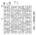
- FIG. 1shows a tree-like clock distribution network 110 designed to distribute a clock signal with a minimum clock skew in an integrated circuit.
- the clock signalis received at a terminal 120 and distributed to terminals 130 at the leaves of tree 110 .
- Terminals 130are connected to inputs of circuit blocks 140 such as registers, flip flops, latches, logic gates, etc.
- the network treeis provided by conductive lines 150 .
- the wires 150 that connect the tree nodes of each given tree level to the tree nodes of any given adjacent levelhave the same dimensions.
- Buffers (amplifiers) 160are located at selected points in the tree to amplify the clock signal.
- each clock path from terminal 120 to a terminal 130has the same dimensions, and the respective buffers 160 in each path are identical to each other. These rules are sometimes violated to compensate for different loading at different terminals 130 .
- the lengths or widths of individual wires 150can be adjusted.
- FIG. 2is a plan view of a grid type clock distribution network.
- Lines 150form a grid, with the horizontal and vertical lines being connected together at the points of intersection.
- the clock signalis delivered to terminal 120 at the grid center, amplified by buffer 160 . 1 , and distributed to buffers 160 . 2 at the grid edges.
- Each buffer 160 . 2drives a horizontal or vertical line 150 .
- Clock terminals 130are positioned on lines 150 and connected to circuit blocks such as blocks 140 of FIG. 1 .
- a circuit block 140 of FIG. 1can be replaced with a grid network or a local clock generation circuit. See U.S. Pat. No. 6,311,313 entitled “X-Y GRID TREE CLOCK DISTRIBUTION NETWORK WITH TUNABLE TREE AND GRID NETWORKS” issued Oct. 30, 2001 to Camporese et al., incorporated herein by reference.
- a perfect placement of a clock distribution network on a semiconductor diecan be difficult due to the presence of other circuitry.
- a modern integrated circuitmay include up to eight metal layers.
- the clock distribution networkuses one of these layers for lines 150 .
- Another metal layer, underlying the lines 150is used for a ground plane or a ground grid to shield the underlying circuitry from the electromagnetic field generated by high frequency clock signals on lines 150 .
- These two layersare separated by a dielectric.
- the speed of signal propagation along the clock distribution networkis affected by the capacitance between the lines 150 and the ground plane or grid.
- the capacitanceis not uniform across the integrated circuit due to local variations of the dielectric thickness and the capacitive coupling between the lines 150 and other nearby switching lines. As a result, it is difficult to control the impedance of lines 150 and therefore the clock propagation speed.
- ground plane or gridconsumes valuable area, increases the cost and complexity of the integrated circuit, and sometimes does not completely eliminate the electromagnetic interference problem because the position of the ground plane or grid can be restricted to allow the same metal layer to be used for other circuit elements.
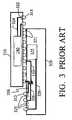
- the clock distribution networkis removed from die 310 containing the clocked circuitry, and placed on a separate (“secondary”) die 320 .
- the dies 310 and 320are bonded together in a flip chip manner with solder balls 321 .
- the two diesare offset from each other so that each die has contact pads not covered by the other die. These contact pads are shown as pads 322 on die 310 and pads 323 on die 320 .
- Pads 322 , 323are connected to external circuitry (not shown) with solder balls 313 .
- die 320can be made larger than die 310 to make room for contact pads 323 . See U.S. Pat. No. 6,040,203 entitled “CLOCK SKEW MINIMIZATION AND METHOD FOR INTEGRATED CIRCUITS”, issued Mar. 21, 2000 to Bozso et al., incorporated herein by reference.
- the inventorhas observed that in the structure of FIG. 3 significant electromagnetic interference, as well as parasitic capacitance, can be associated with the transfer of signals and power and ground voltages between contact pads 322 , 323 and circuit blocks in dies 310 and 320 .
- the signal, power, and ground paths between contact pads 322 and blocks 140go through conductive lines 324 .
- the signal, power and ground paths between contact pads 323 and circuit 310 , and the paths between contact pads 323 and circuitry 325 in die 320go through conductive lines 326 .
- the lines 324 , 326can be parallel to lines 150 , or make small angles with lines 150 . The small angles when combined with small spacing between a line 324 or 326 and a line 150 may lead to significant electromagnetic interference and parasitic capacitance.
- some or all of the contact pads 323are moved to the bottom of die 320 .
- the bottom contact pads 323are connected to circuitry at the top of the die by means of conductive features forming large angles (e.g. 90°) with the top and bottom surfaces of die 310 . Since large portions of lines 150 extend along the top surface of die 310 , the electromagnetic interference and the parasitic capacitance can be reduced.
- contact pads 322are omitted.
- the conductive paths to and from die 310are through die 320 . Further reduction of the electromagnetic interference and the parasitic capacitance can be achieved as a result. Also, the structure occupies less area.
- the bottom contact pads on die 320can be bonded to contact pads on another integrated circuit or a wiring substrate.
- the die 320serves as a semiconductor “interposer” positioned between die 310 and other integrated circuits or between die 310 and a wiring substrate.
- Die 320may include ground planes or grids or other grounded lines to shield the circuitry above and below the interposer from the clock distribution network.
- interposersare provided, with different parts of a clock distribution network on different interposers.
- the clock distribution lines 150( FIGS. 1 , 2 ) are formed in trenches etched in a semiconductor substrate.
- the RC value of lines 150can be lowered by making the trenches deeper, without increasing the lateral area occupied by the RC lines. Also, the RC value, and hence the clock skew, become more controllable.
- conductive linesnot belonging to the clock distribution network, can be formed in such trenches.
- FIGS. 1 and 2are plan views that illustrate prior art clock distribution networks.
- FIG. 3is a side view illustrating a prior art structure.
- FIGS. 4 and 5are cross sectional views of embodiments of the present invention.
- FIG. 6is a schematic diagram illustrating an embodiment of the present invention.
- FIGS. 7 and 8are cross sectional views of some embodiments of the present invention.
- FIG. 9is a top view of an embodiment of the present invention.
- FIGS. 10–11are cross sectional views of some embodiments of the present invention.
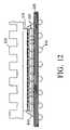
- FIG. 12is a side view of one embodiment of the present invention.
- FIG. 13is a cross sectional view of one embodiment of the present invention.
- FIG. 14Ais a side view of one embodiment of the present invention.
- FIG. 14Bis a bottom view of the structure of FIG. 14A .
- FIGS. 15A–15D , 16 , 17 A– 17 Dare cross sectional view of embodiments of the present invention in the process of fabrication.
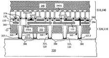
- FIG. 4illustrates an integrated circuit 310 mounted on another integrated circuit 320 which in turn is mounted on a wiring substrate 330 .
- Each of circuits 310 , 320is a semiconductor die or wafer, or some portion of a semiconductor wafer.
- Circuit 310includes clocked circuitry 140 and may also include non-clocked circuitry.
- circuit 310may include a microprocessor, a memory, a digital controller, and so on.
- Circuit 320is an interposer that contains clock distribution networks 110 .
- the clock distribution networkscan be of any type, including the types shown in FIGS. 1 , 2 , or other types, known or to be invented.
- Circuit 310includes a semiconductor substrate 340 .
- Active areas 340 Amay have been formed in substrate 340 for transistors, resistors, capacitors, interconnect lines, or other circuit elements.
- Interposer 320includes a semiconductor substrate 350 .
- Conductive lines 150have been formed from one or more metal layers deposited over substrate 350 and insulated from the substrate by insulating layers.
- An insulating layermay include one or more dielectric layers, a stack of dielectric and semiconductor layers, and other insulating structures, known or to be invented.
- lines 150can be formed from diffused (doped) areas of substrate 350 , or a combination of metal layers and diffused areas, or from other conductive materials, using any suitable techniques, known or to be invented.
- Clock terminals 130are contact pads formed at the top surface of interposer 320 .
- Clock input terminals 120are provided by contact pads 323 located at the bottom surface of interposer 320 .
- the clock terminalsare inputs to clock distribution networks.
- Holes 360pass through substrate 350 between its top and bottom surfaces.
- Conductive featuresare formed in through holes 360 to connect the clock input terminals 120 , and possibly other terminals 323 at the bottom of interposer 320 , to contact pads and/or circuitry at the top of the interposer.
- the conductive featuresare insulated from substrate 350 by dielectric 370 .
- Suitable techniques for forming such conductive featuresare described in U.S. Pat. No. 6,322,903 issued Nov. 27, 2001 to O. Siniaguine et al. and incorporated herein by reference. Other techniques, known or to be invented, can be also used.
- the conductive featurescan be metal plugs or thin films deposited over sidewalls of holes 360 over dielectric 370 .
- the conductive featurescan be perpendicular to the top and bottom surfaces of circuit 320 or substrate 340 , or the conductive features can form large angles with these surfaces. These angles are at least 80° in some embodiments, or at least 45°, or at least 30°. Other angles are possible.
- Circuit 310is bonded to interposer 320 in a flip chip manner, with the active areas 340 A at the bottom of substrate 340 .
- Contact pads 374 on the bottom of circuit 310are bonded to contact pads on the top of circuit 320 . Some of contact pads 374 are inputs of circuit blocks 140 ( FIG. 1 ). These contact pads 374 are bonded to pads 130 . Other contact pads 374 are bonded to other contact pads 380 at the top of interposer 320 .
- Contact pads 380can be connected, by conductive features in holes 360 , to contact pads 323 (i.e. contact pads 323 . 1 , 323 . 2 , 323 . 3 etc.) on the bottom of interposer 320 . In one example, contact pad 323 .
- Contact pad 323 . 3is a ground input.
- Contact pad 323 . 2an input, output, or input/output terminal for a signal.
- the inventionis not limited to any particular signals that can be routed through interposer 320 .
- Contact pads 323are bonded to pads 388 on wiring substrate 330 .
- circuit 310 to interposer 320can be accomplished with solder, thermocompression, conductive or anisotropic adhesive, or any other technique, known or to be invented. The same techniques, or other techniques, can be used to bond the contact pads 323 to pads 388 .
- Active areas 340 Amay be positioned at the top of circuit 310 .
- Circuit 310may include contact pads both at the top and at the bottom, with through holes going through substrate 340 to provide suitable interconnections.
- Other integrated circuits(not shown), including other interposers, can be bonded to contact pads on top of circuit 310 . See the aforementioned U.S. Pat. No. 6,322,903. These other integrated circuits may contain parts of clock distribution networks.
- the integrated circuitsmay be bonded to each other in any configurations, not necessarily in a stack one above the other. For example, multiple circuits 310 can be bonded side by side to the top surface of interposer 320 . Multiple interposers may be present, and they may contain different parts of clock distribution networks, or different clock distribution networks.
- FIG. 5shows a similar structure but with interposer 320 containing a ground structure 390 .
- Structure 390can be a ground plane, i.e. a conductive feature that is wider than a line 150 .
- Structure 390can be a ground grid (a grid of grounded conductive lines) or may consist of just a few (possibly one) grounded lines.
- Structure 390may include multiple ground planes or grids.
- Structure 390shields the circuit 310 from noise generated by the clock distribution networks.
- Structure 390can be formed from a metal layer or layers overlying the lines 150 .
- Structure 390is connected to contact pad 323 . 3 and is insulated from lines 150 by dielectric.
- Structure 390is interrupted to make room for contacts 394 that connect contact pads 130 , 380 at the top of interposer 320 to lines 150 and other features in the interposer.
- Ground structure 390may extend over almost all of substrate 350 , or at least almost all of the clock distribution networks.
- structure 390is held at a constant non-ground voltage.
- shielding structure 390Due to the presence of shielding structure 390 , it is less important to have a ground plane in circuit 310 .
- the number of metal layers in circuit 310can therefore be reduced.
- the incremental cost of each additional metal layerincreases with the total number of metal layers in an integrated circuit, so moving a ground plane from circuit 310 to circuit 320 may reduce the total manufacturing cost.
- active areas 350 Amay be formed in substrate 350 for transistors or other elements of “clock headers” 160 (such as shown in FIGS. 1 , 2 ).
- Clock headers 160can be amplifiers, clock dividers or multipliers, phase shifters, or other clock circuitry.
- active areas 350 Aare located at the top surface of substrate 350 , but this is not necessary. Similar active areas and clock headers can be formed in the structure of FIG. 4 .
- At least some contact pads 380are positioned above the respective holes 360 and are connected to respective contact pads 323 without use of horizontal conductive lines.
- a contact pad 380can however be laterally spaced from the respective hole 360 , and connected to the respective contact pad 323 by a combination of a conductive feature in the hole 360 and horizontal lines.
- Substrate 350is grounded, or held at some other constant voltage, to shield the clock distribution networks from the circuitry in wiring substrate 330 and vice versa.
- the active areas 350 Ado not have to be grounded, but the grounded portion of substrate 350 extends laterally throughout the substrate in some embodiments.
- Interposer 320may contain only a part of a clock distribution network.
- interposer 320may contain only a sub-tree 110 S ( FIG. 6 ) of a tree network 110 .
- Sub-tree 110 Sconsists of a number of tree levels including the root 120 .
- the rest of network 110may be in circuit 310 .
- interposer 320contains an additional ground structure 510 .
- Thismay be a ground plane or grid or any other type similar to structure 390 .
- Ground structure 510is located between clock distribution lines 150 and substrate 350 .
- structure 510is held at a constant non-ground voltage.
- Substrate 350is not necessarily held at a constant voltage.
- interposer 320contains only the clock distribution network or networks, so its fabrication is relatively inexpensive. In other embodiments, interposer 320 also contains decoupling capacitors, diodes, resistors, transistors, and other elements. In some embodiments, the fabrication yield of the entire structure is increased because the fabrication of the clock distribution network does not have to be integrated with the fabrication of circuit 310 except at the packaging stage.
- FIG. 8is a cross sectional view illustrating fabrication of lines 150 in one embodiment.
- Trenches 610are etched in substrate 350 .
- Dielectric film 620is formed on the substrate.
- Dielectric 620covers the trench surfaces.
- a metal layer 624e.g. tungsten, aluminum or copper, is deposited to fill the trenches and possibly cover the substrate. If metal 624 covers the substrate, the metal is removed from above the substrate by chemical mechanical polishing (CMP), electrochemical polishing, etching, or some other method.
- CMPchemical mechanical polishing
- the trenchesremain filled with metal 624 , which provides the lines 150 .
- the trenchesmay form a tree or grid network as in FIG. 1 or 2 , or some other network.
- Metal 624provides a corresponding conductive network.
- metal 624fills the trenches only partially.
- Metal 624can be a thin film on the trench surfaces.
- metal 624can be replaced with multiple metal layers separated by dielectric. Different metal layers may provide different lines 150 in the same trench. Alternatively, different metal layers may be interconnected to provide a single line 150 . Use of multiple metal layers instead of a single layer filling the trench reduces thermomechanical stress. Two of the metal layers in a trench can be used for the opposite phases of a differential clock signal. Alternatively, the opposite phases can be implemented by metal lines formed in adjacent trenches running in parallel.
- substrate 350is monocrystalline silicon.
- Trenches 610have a width W of about 0.1 ⁇ m to 10 ⁇ m and a depth D of 1 to 20 ⁇ m. The length of the trenches is determined by lines 150 .
- Dielectric 620is silicon dioxide, silicon nitride, or some other dielectric, possible having a low dielectric constant. Dielectric 620 can also contain air gaps. See U.S. Pat. No. 6,265,321 issued Jul. 24, 2001, entitled “AIR BRIDGE PROCESS FOR FORMING AIR GAPS”, incorporated herein by reference.
- An exemplary thickness of dielectric 620is 0.1–5 ⁇ m.
- Dielectric 620can be formed by thermal oxidation, chemical vapor deposition (CVD), or other techniques, known or to be invented. Dimensions other than those mentioned above are also possible. The width W and the other dimensions may vary from one line 150 to another in the same interposer.
- the capacitance associated with lines 150has the following components: (i) the capacitance C sub between lines 150 and substrate 350 , and (ii) the capacitance C cir between lines 150 and other circuit elements, e.g. elements of amplifiers 160 . Due to the lines 150 being formed in the trenches, the substrate component C sub becomes a greater portion of the total capacitance. The substrate component C sub is easy to control—if the areas of substrate 350 adjacent to lines 150 are held at a constant voltage, the substrate component C sub is largely a function of the trench dimensions, independent of the placement of the other circuit elements. Therefore, the clock propagation time becomes more controllable.
- the RC valuecan be reduced by increasing the trench depth D without increasing the lateral area occupied by the clock distribution network.
- Dis increased by some factor K
- the resistance R of lines 150is reduced by the same factor K.
- the capacitance component associated with the sidewalls of lines 150increases by the same factor K, but the capacitance associated with the top and bottom surfaces of lines 150 does not change. Therefore, the total capacitance increase does not offset the reduced resistance.
- clock distribution lines 150cannot be formed in trenches in a semiconductor substrate because large portions of the substrate are taken by active areas. Moving the clock distribution networks, or parts of the clock distribution networks, to the interposer facilitates fabrication of lines 150 in the trenches.
- interposer 320is absent.
- a part or all of clock distribution lines 150is formed in trenches in substrate 340 .
- dielectric 630is formed over metal 150 .
- Ground structure 390is formed from a metal layer on dielectric 630 .
- conductive linesnot necessarily parts of clock distribution networks, can be formed in trenches in the substrate.
- conductive line 624 in trench 610interconnects two laterally spaced nodes of circuit blocks 140 . 1 , 140 . 2 .
- Blocks 140 . 1 , 140 . 2can be any circuits, clocked or non-clocked.
- the structure of FIG. 9may be part of circuit 310 or 320 .
- a metal line 624 in a trench 610 in substrate 350can be connected to a contact pad 323 on the bottom of semiconductor substrate 350 by a conductive feature in a hole 360 passing through the substrate at the bottom of the trench.
- FIG. 11shows an interposer 320 with two ground structures 390 , 510 (as in FIG. 7 ).
- Trenches 610 and dielectric 620are formed as in FIG. 8 .
- a metal layer 510is deposited to provide a ground structure underneath the lines 150 .
- Metal 510covers the entire surface of substrate 350 , including the surfaces of the trenches.
- the trenchesare 1 ⁇ m wide and 1 to 20 ⁇ m deep, and metal 510 is aluminum copper, tantalum, titanium, or some other metal 0.01 ⁇ m to 2 ⁇ m thick.
- Metal 510can be patterned as desired to make room for clock headers 160 and other circuitry, and/or provide circuit elements that are not necessarily part of a ground structure.
- dielectric 710is deposited.
- silicon dioxide, silicon nitride, a low-k (low dielectric constant) dielectric, or a stack of different dielectric and semiconductor materialscan be formed to a thickness of 0.01–2 ⁇ m by CVD.
- Dielectric 710can be patterned as desired.
- metal 624is deposited as described above in connection with FIG. 8 .
- Metal 624provides the lines 150 .
- Metal 624is insulated from metal 510 by dielectric 710 .
- dielectric 714is deposited and patterned as desired.
- Dielectric 714covers the metal lines 150 .
- Contact openings 720are etched in dielectric 710 and, possibly, dielectric 714 , to expose metal 510 outside of trenches 610 .
- metal 390e.g. cobalt, aluminum, copper, or some other material, is deposited over the structure and patterned as desired. Metal 390 overlies the lines 150 and contacts the metal 510 in openings 720 . In some embodiments, metal 390 extends over the entire length of lines 150 . Metal layers 390 , 510 provide ground structures above and below the lines 150 .
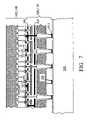
- FIG. 12illustrates exemplary packaging.
- Thisis a conventional ball grid array (BGA) package.
- Wiring substrate 330is a BGA substrate (e.g. plastic) with solder balls 810 on the bottom.
- Heat sink 820is placed on circuit 310 .
- Underfill 830fills the area between the circuits 310 , 320 and the area between interposer 320 and substrate 330 .
- Other packaging techniquesknown or to be invented, can also be used.
- Additional integrated circuitse.g. memory, logic, RF circuits
- passive componentse.g. decoupling capacitors, filters
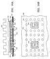
- wiring substrate 330has a cavity or through hole 910 .
- Integrated circuit 920is bonded to the bottom of interposer 320 and is located in the cavity or through hole 910 .
- Contact pads 120 , 323 on the bottom of interposer 320are bonded to contact pads at the top of circuit 920 and wiring substrate 330 .
- Some or all of the clock distribution circuitrymay be located in circuit 920 .
- FIGS. 14A , 14 Bare side and bottom views, respectively, of a packaged BGA structure. This structure combines the features of the structures of FIGS. 12 and 13 .
- Wiring substrate 330has two through holes 910 .
- An integrated circuit 920is positioned in each of the through holes and bonded to interposer 320 , as in FIG. 13 .
- FIGS. 15A–15Dillustrate an exemplary manufacturing process.
- Multiple integrated circuits 310are flip-chip bonded to wafer 320 W, as shown in FIG. 15A .
- Wafer 320 Wwill be diced into interposers 320 .
- Wafer 320 Whas been processed to form openings 360 and contacts 323 , but the openings are not yet through holes, and the contacts 323 are not exposed.
- Contact pads 1510(shown only in FIG. 15A for simplicity) on top of wafer 320 W between circuits 310 are used to test the circuitry after the flip-chip bonding.
- the areas between the adjacent circuits 310 , and the areas between the circuits 310 and the interposer wafer 320 W,are filled with a flowable material 1520 ( FIG. 15B ), such as commonly used for underfill. Suitable materials include polymers, epoxies, BCB (Benzocyclobutene). Fill material 1520 is cured by known techniques. Layer 1520 is shown flush with the top surface of circuits 310 , but this is not necessary. The top surface of layer 1520 may be below the top surface of circuits 310 , or the layer 1520 may cover the circuits 310 .
- Interposer wafer 320 Wis thinned on the bottom to expose the contacts 323 ( FIG. 15C ).
- An exemplary thickness of the thinned wafer 320 Wis 10–200 ⁇ m, and other dimensions are possible. Exemplary thinning processes are described in U.S. Pat. No. 6,322,903 issued Nov. 27, 2001 to Siniaguine et al., incorporated herein by reference. Circuits 310 and fill 1520 increase the rigidity of the structure and prevent bowing, warping, or other deformation of wafer 320 W. Consequently, damage to the wafer becomes less likely.
- Wafer 320 Wis diced into individual interposers 320 ( FIG. 15D ) along scribe lines located between the circuits 310 .
- the dicingcan involve any suitable techniques (e.g. sawing, scribing, laser, water jet cut, or other techniques, known or to be invented).
- Each interposer 320may have the same lateral dimensions as the corresponding circuit 310 .
- circuit 310is smaller than the interposer.
- FIGS. 17A–17Dare similar to the process of FIGS. 15A–15D , and each of FIGS. 17A–17D shows the same stage as the respective FIG. 15A–15D .
- grooves 1710are formed in wafer 320 W along the scribe lines.
- the groovesmay be formed by etching, sawing, or any other suitable technique.
- the groovesare at least as deep as the final thickness of interposers 320 after the interposer thinning ( FIG. 17C ).
- the groove widthis greater than the width of the cut made at the dicing stage of FIG. 17D .
- Fill material 1520may or may not fill the grooves at the stage of FIG. 17B .
- the groovesbecome exposed on the bottom ( FIG. 17C ), but the fill 1520 holds the interposers 320 together until the dicing stage of FIG. 17D . Because the interposers 320 are held together, handling of the structure after the thinning step is simplified. At the dicing stage, the edges of the interposers 320 are less likely to be damaged by the dicing tool. Also, if the wafer 320 W is thinned by a wet or dry etch, and if the fill material does not reach to the bottom of grooves 1710 or the fill material is etched faster than the wafer 320 W, then the bottom corners and edges of interposers 320 will be rounded and less prone to chipping.
Landscapes
- Engineering & Computer Science (AREA)
- Microelectronics & Electronic Packaging (AREA)
- Physics & Mathematics (AREA)
- General Physics & Mathematics (AREA)
- Computer Hardware Design (AREA)
- Power Engineering (AREA)
- Condensed Matter Physics & Semiconductors (AREA)
- Manufacturing & Machinery (AREA)
- Geometry (AREA)
- Theoretical Computer Science (AREA)
- General Engineering & Computer Science (AREA)
- Semiconductor Integrated Circuits (AREA)
Abstract
Description
Claims (17)
Priority Applications (1)
| Application Number | Priority Date | Filing Date | Title |
|---|---|---|---|
| US11/131,711US7173327B2 (en) | 2002-04-18 | 2005-05-18 | Clock distribution networks and conductive lines in semiconductor integrated circuits |
Applications Claiming Priority (4)
| Application Number | Priority Date | Filing Date | Title |
|---|---|---|---|
| US10/127,144US6730540B2 (en) | 2002-04-18 | 2002-04-18 | Clock distribution networks and conductive lines in semiconductor integrated circuits |
| US10/375,208US20040081153A1 (en) | 2000-11-08 | 2003-02-17 | System and method for improving the efficiency of routers on the internet and/or cellular networks and/or other networks and alleviating bottlenecks and overloads on the network |
| US10/956,827US20050051887A1 (en) | 2002-04-18 | 2004-10-01 | Clock distribution networks and conductive lines in semiconductor integrated circuits |
| US11/131,711US7173327B2 (en) | 2002-04-18 | 2005-05-18 | Clock distribution networks and conductive lines in semiconductor integrated circuits |
Related Parent Applications (1)
| Application Number | Title | Priority Date | Filing Date |
|---|---|---|---|
| US10/956,827DivisionUS20050051887A1 (en) | 2002-04-18 | 2004-10-01 | Clock distribution networks and conductive lines in semiconductor integrated circuits |
Publications (2)
| Publication Number | Publication Date |
|---|---|
| US20050207238A1 US20050207238A1 (en) | 2005-09-22 |
| US7173327B2true US7173327B2 (en) | 2007-02-06 |
Family
ID=29215193
Family Applications (5)
| Application Number | Title | Priority Date | Filing Date |
|---|---|---|---|
| US10/127,144Expired - LifetimeUS6730540B2 (en) | 2002-04-18 | 2002-04-18 | Clock distribution networks and conductive lines in semiconductor integrated circuits |
| US10/375,218AbandonedUS20030197239A1 (en) | 2002-04-18 | 2003-02-26 | Clock distribution networks and conductive lines in semiconductor integrated circuits |
| US10/956,827AbandonedUS20050051887A1 (en) | 2002-04-18 | 2004-10-01 | Clock distribution networks and conductive lines in semiconductor integrated circuits |
| US11/131,711Expired - LifetimeUS7173327B2 (en) | 2002-04-18 | 2005-05-18 | Clock distribution networks and conductive lines in semiconductor integrated circuits |
| US11/559,805AbandonedUS20070069377A1 (en) | 2002-04-18 | 2006-11-14 | Clock distribution networks and conductive lines in semiconductor integrated circuits |
Family Applications Before (3)
| Application Number | Title | Priority Date | Filing Date |
|---|---|---|---|
| US10/127,144Expired - LifetimeUS6730540B2 (en) | 2002-04-18 | 2002-04-18 | Clock distribution networks and conductive lines in semiconductor integrated circuits |
| US10/375,218AbandonedUS20030197239A1 (en) | 2002-04-18 | 2003-02-26 | Clock distribution networks and conductive lines in semiconductor integrated circuits |
| US10/956,827AbandonedUS20050051887A1 (en) | 2002-04-18 | 2004-10-01 | Clock distribution networks and conductive lines in semiconductor integrated circuits |
Family Applications After (1)
| Application Number | Title | Priority Date | Filing Date |
|---|---|---|---|
| US11/559,805AbandonedUS20070069377A1 (en) | 2002-04-18 | 2006-11-14 | Clock distribution networks and conductive lines in semiconductor integrated circuits |
Country Status (1)
| Country | Link |
|---|---|
| US (5) | US6730540B2 (en) |
Cited By (14)
| Publication number | Priority date | Publication date | Assignee | Title |
|---|---|---|---|---|
| US20100182045A1 (en)* | 2009-01-22 | 2010-07-22 | Broadcom Corporation | Low-jitter high-frequency clock channel |
| US8431431B2 (en) | 2011-07-12 | 2013-04-30 | Invensas Corporation | Structures with through vias passing through a substrate comprising a planar insulating layer between semiconductor layers |
| US8757897B2 (en) | 2012-01-10 | 2014-06-24 | Invensas Corporation | Optical interposer |
| US20140264839A1 (en)* | 2013-03-15 | 2014-09-18 | Taiwan Semiconductor Manufacturing Company, Ltd. | Packaged Semiconductor Devices, Methods of Packaging Semiconductor Devices, and PoP Devices |
| US8984463B2 (en) | 2012-11-28 | 2015-03-17 | Qualcomm Incorporated | Data transfer across power domains |
| US9018094B2 (en) | 2011-03-07 | 2015-04-28 | Invensas Corporation | Substrates with through vias with conductive features for connection to integrated circuit elements, and methods for forming through vias in substrates |
| US9041448B2 (en) | 2013-03-05 | 2015-05-26 | Qualcomm Incorporated | Flip-flops in a monolithic three-dimensional (3D) integrated circuit (IC) (3DIC) and related methods |
| US9064077B2 (en) | 2012-11-28 | 2015-06-23 | Qualcomm Incorporated | 3D floorplanning using 2D and 3D blocks |
| US20150206855A1 (en)* | 2014-01-22 | 2015-07-23 | Mediatek Inc. | Semiconductor package |
| US9171608B2 (en) | 2013-03-15 | 2015-10-27 | Qualcomm Incorporated | Three-dimensional (3D) memory cell separation among 3D integrated circuit (IC) tiers, and related 3D integrated circuits (3DICS), 3DIC processor cores, and methods |
| US9177890B2 (en) | 2013-03-07 | 2015-11-03 | Qualcomm Incorporated | Monolithic three dimensional integration of semiconductor integrated circuits |
| US9323010B2 (en) | 2012-01-10 | 2016-04-26 | Invensas Corporation | Structures formed using monocrystalline silicon and/or other materials for optical and other applications |
| US9536840B2 (en) | 2013-02-12 | 2017-01-03 | Qualcomm Incorporated | Three-dimensional (3-D) integrated circuits (3DICS) with graphene shield, and related components and methods |
| US9748106B2 (en)* | 2016-01-21 | 2017-08-29 | Micron Technology, Inc. | Method for fabricating semiconductor package |
Families Citing this family (62)
| Publication number | Priority date | Publication date | Assignee | Title |
|---|---|---|---|---|
| US7271489B2 (en) | 2003-10-15 | 2007-09-18 | Megica Corporation | Post passivation interconnection schemes on top of the IC chips |
| JP4110390B2 (en)* | 2002-03-19 | 2008-07-02 | セイコーエプソン株式会社 | Manufacturing method of semiconductor device |
| JP2004079701A (en)* | 2002-08-14 | 2004-03-11 | Sony Corp | Semiconductor device and its manufacturing method |
| US7470564B2 (en)* | 2002-10-28 | 2008-12-30 | Intel Corporation | Flip-chip system and method of making same |
| KR100541393B1 (en)* | 2003-04-26 | 2006-01-10 | 삼성전자주식회사 | Multichip BA Package |
| US7279783B1 (en)* | 2003-10-29 | 2007-10-09 | Silicon Pipe, Inc. | Partitioned integrated circuit package with central clock driver |
| US7049170B2 (en)* | 2003-12-17 | 2006-05-23 | Tru-Si Technologies, Inc. | Integrated circuits and packaging substrates with cavities, and attachment methods including insertion of protruding contact pads into cavities |
| US7060601B2 (en)* | 2003-12-17 | 2006-06-13 | Tru-Si Technologies, Inc. | Packaging substrates for integrated circuits and soldering methods |
| US7075365B1 (en) | 2004-04-22 | 2006-07-11 | Altera Corporation | Configurable clock network for programmable logic device |
| JP4353861B2 (en)* | 2004-06-30 | 2009-10-28 | Necエレクトロニクス株式会社 | Semiconductor device |
| US8130560B1 (en) | 2006-11-13 | 2012-03-06 | Google Inc. | Multi-rank partial width memory modules |
| US8089795B2 (en) | 2006-02-09 | 2012-01-03 | Google Inc. | Memory module with memory stack and interface with enhanced capabilities |
| US8327104B2 (en) | 2006-07-31 | 2012-12-04 | Google Inc. | Adjusting the timing of signals associated with a memory system |
| US8081474B1 (en) | 2007-12-18 | 2011-12-20 | Google Inc. | Embossed heat spreader |
| US9542352B2 (en) | 2006-02-09 | 2017-01-10 | Google Inc. | System and method for reducing command scheduling constraints of memory circuits |
| US8335894B1 (en) | 2008-07-25 | 2012-12-18 | Google Inc. | Configurable memory system with interface circuit |
| US7609567B2 (en) | 2005-06-24 | 2009-10-27 | Metaram, Inc. | System and method for simulating an aspect of a memory circuit |
| US8055833B2 (en) | 2006-10-05 | 2011-11-08 | Google Inc. | System and method for increasing capacity, performance, and flexibility of flash storage |
| US8041881B2 (en) | 2006-07-31 | 2011-10-18 | Google Inc. | Memory device with emulated characteristics |
| US8060774B2 (en) | 2005-06-24 | 2011-11-15 | Google Inc. | Memory systems and memory modules |
| US8359187B2 (en) | 2005-06-24 | 2013-01-22 | Google Inc. | Simulating a different number of memory circuit devices |
| US8386722B1 (en) | 2008-06-23 | 2013-02-26 | Google Inc. | Stacked DIMM memory interface |
| US8244971B2 (en) | 2006-07-31 | 2012-08-14 | Google Inc. | Memory circuit system and method |
| US8397013B1 (en) | 2006-10-05 | 2013-03-12 | Google Inc. | Hybrid memory module |
| US9171585B2 (en) | 2005-06-24 | 2015-10-27 | Google Inc. | Configurable memory circuit system and method |
| US9507739B2 (en) | 2005-06-24 | 2016-11-29 | Google Inc. | Configurable memory circuit system and method |
| US7386656B2 (en) | 2006-07-31 | 2008-06-10 | Metaram, Inc. | Interface circuit system and method for performing power management operations in conjunction with only a portion of a memory circuit |
| US8796830B1 (en) | 2006-09-01 | 2014-08-05 | Google Inc. | Stackable low-profile lead frame package |
| US20080028136A1 (en)* | 2006-07-31 | 2008-01-31 | Schakel Keith R | Method and apparatus for refresh management of memory modules |
| US8111566B1 (en) | 2007-11-16 | 2012-02-07 | Google, Inc. | Optimal channel design for memory devices for providing a high-speed memory interface |
| US10013371B2 (en) | 2005-06-24 | 2018-07-03 | Google Llc | Configurable memory circuit system and method |
| US8090897B2 (en)* | 2006-07-31 | 2012-01-03 | Google Inc. | System and method for simulating an aspect of a memory circuit |
| US8438328B2 (en)* | 2008-02-21 | 2013-05-07 | Google Inc. | Emulation of abstracted DIMMs using abstracted DRAMs |
| US8077535B2 (en) | 2006-07-31 | 2011-12-13 | Google Inc. | Memory refresh apparatus and method |
| US20080082763A1 (en) | 2006-10-02 | 2008-04-03 | Metaram, Inc. | Apparatus and method for power management of memory circuits by a system or component thereof |
| WO2007028109A2 (en) | 2005-09-02 | 2007-03-08 | Metaram, Inc. | Methods and apparatus of stacking drams |
| US7475374B1 (en) | 2005-12-20 | 2009-01-06 | Advanced Micro Devices, Inc. | Clock grid driven by virtual leaf drivers |
| US9632929B2 (en) | 2006-02-09 | 2017-04-25 | Google Inc. | Translating an address associated with a command communicated between a system and memory circuits |
| US7859117B2 (en)* | 2007-02-27 | 2010-12-28 | Taiwan Semiconductor Manufacturing Company, Ltd. | Clocking architecture in stacked and bonded dice |
| US8080874B1 (en)* | 2007-09-14 | 2011-12-20 | Google Inc. | Providing additional space between an integrated circuit and a circuit board for positioning a component therebetween |
| US20090091017A1 (en)* | 2007-10-09 | 2009-04-09 | Fjelstad Joseph C | Partitioned Integrated Circuit Package with Central Clock Driver |
| US20090212420A1 (en)* | 2008-02-22 | 2009-08-27 | Harry Hedler | integrated circuit device and method for fabricating same |
| KR101458958B1 (en)* | 2008-06-10 | 2014-11-13 | 삼성전자주식회사 | Semiconductor chip, semiconductor package, and method of fabricating the semiconductor chip |
| US8749027B2 (en)* | 2009-01-07 | 2014-06-10 | Taiwan Semiconductor Manufacturing Company, Ltd. | Robust TSV structure |
| DE202010017690U1 (en) | 2009-06-09 | 2012-05-29 | Google, Inc. | Programming dimming terminating resistor values |
| US8601306B1 (en) | 2010-06-22 | 2013-12-03 | Xilinx, Inc. | Decryption of configuration data for multi-die integrated circuits |
| US8058897B1 (en) | 2010-06-28 | 2011-11-15 | Xilinx, Inc. | Configuration of a multi-die integrated circuit |
| US8901747B2 (en) | 2010-07-29 | 2014-12-02 | Mosys, Inc. | Semiconductor chip layout |
| US20120074562A1 (en)* | 2010-09-24 | 2012-03-29 | Taiwan Semiconductor Manufacturing Company, Ltd. | Three-Dimensional Integrated Circuit Structure with Low-K Materials |
| US8927909B2 (en)* | 2010-10-11 | 2015-01-06 | Stmicroelectronics, Inc. | Closed loop temperature controlled circuit to improve device stability |
| KR20130082344A (en)* | 2012-01-11 | 2013-07-19 | 에스케이하이닉스 주식회사 | Semiconductor memory device, memory chip, memory module, memory system and method for fabricating emiconductor memory device |
| US8933544B2 (en)* | 2012-07-12 | 2015-01-13 | Omnivision Technologies, Inc. | Integrated circuit stack with integrated electromagnetic interference shielding |
| US9091727B1 (en) | 2012-10-16 | 2015-07-28 | Xilinx, Inc. | Configuration and testing of multiple-die integrated circuits |
| US20140175619A1 (en)* | 2012-12-20 | 2014-06-26 | Nvidia Corporation | Stripline and reference plane implementation for interposers using an implant layer |
| US9543965B1 (en)* | 2013-10-04 | 2017-01-10 | Altera Corporation | Interposer with embedded clock network circuitry |
| JP6798252B2 (en)* | 2016-10-31 | 2020-12-09 | 住友電気工業株式会社 | High frequency device |
| US10418311B2 (en) | 2017-03-28 | 2019-09-17 | Micron Technology, Inc. | Method of forming vias using silicon on insulator substrate |
| JP2018182213A (en)* | 2017-04-19 | 2018-11-15 | 富士通株式会社 | Semiconductor device and method of manufacturing semiconductor device |
| US11500412B2 (en) | 2019-03-28 | 2022-11-15 | Intel Corporation | Techniques for clock signal transmission in integrated circuits and interposers |
| JP7351266B2 (en)* | 2020-07-07 | 2023-09-27 | 信越半導体株式会社 | Manufacturing method of semiconductor device |
| US20230095162A1 (en)* | 2021-09-24 | 2023-03-30 | Intel Corporation | Semiconductor Devices and Methods for Forming a Semiconductor Device |
| US20250015118A1 (en)* | 2021-11-04 | 2025-01-09 | Sony Semiconductor Solutions Corporation | Light detection apparatus and electronic apparatus |
Citations (35)
| Publication number | Priority date | Publication date | Assignee | Title |
|---|---|---|---|---|
| EP0254046A1 (en) | 1986-07-15 | 1988-01-27 | International Business Machines Corporation | Semiconductor memory |
| EP0280848A2 (en) | 1987-03-02 | 1988-09-07 | International Business Machines Corporation | On-chip on-line ac and dc clock tree error detection system |
| US5001525A (en) | 1989-03-27 | 1991-03-19 | International Business Machines Corporation | Two square memory cells having highly conductive word lines |
| US5057895A (en) | 1990-08-06 | 1991-10-15 | Harris Corporation | Trench conductor and crossunder architecture |
| US5119155A (en)* | 1989-11-29 | 1992-06-02 | Kabushiki Kaisha Toshiba | Semiconductor memory device with dielectric isolation |
| US5177594A (en) | 1991-01-09 | 1993-01-05 | International Business Machines Corporation | Semiconductor chip interposer module with engineering change wiring and distributed decoupling capacitance |
| US5251097A (en) | 1990-06-11 | 1993-10-05 | Supercomputer Systems Limited Partnership | Packaging architecture for a highly parallel multiprocessor system |
| US5416861A (en) | 1994-04-29 | 1995-05-16 | University Of Cincinnati | Optical synchronous clock distribution network and high-speed signal distribution network |
| US5466963A (en) | 1994-01-13 | 1995-11-14 | Harris Corporation | Trench resistor architecture |
| US5501006A (en) | 1993-09-22 | 1996-03-26 | Motorola, Inc. | Method for connection of signals to an integrated circuit |
| US5665989A (en) | 1995-01-03 | 1997-09-09 | Lsi Logic | Programmable microsystems in silicon |
| US5761350A (en) | 1997-01-22 | 1998-06-02 | Koh; Seungug | Method and apparatus for providing a seamless electrical/optical multi-layer micro-opto-electro-mechanical system assembly |
| US5811868A (en) | 1996-12-20 | 1998-09-22 | International Business Machines Corp. | Integrated high-performance decoupling capacitor |
| US5933717A (en) | 1997-03-04 | 1999-08-03 | Advanced Micro Devices, Inc. | Vertical transistor interconnect structure and fabrication method thereof |
| JP2000058545A (en)* | 1998-08-03 | 2000-02-25 | Sony Corp | Semiconductor device and distribution method for clock signal |
| US6037822A (en)* | 1997-09-30 | 2000-03-14 | Intel Corporation | Method and apparatus for distributing a clock on the silicon backside of an integrated circuit |
| US6040203A (en) | 1996-08-20 | 2000-03-21 | International Business Machines Corporation | Clock skew minimization and method for integrated circuits |
| US6175160B1 (en) | 1999-01-08 | 2001-01-16 | Intel Corporation | Flip-chip having an on-chip cache memory |
| US6222246B1 (en) | 1999-01-08 | 2001-04-24 | Intel Corporation | Flip-chip having an on-chip decoupling capacitor |
| US6236079B1 (en) | 1997-12-02 | 2001-05-22 | Kabushiki Kaisha Toshiba | Dynamic semiconductor memory device having a trench capacitor |
| US20010006233A1 (en) | 1997-02-25 | 2001-07-05 | Vallett David P. | Semiconductor devices having backside probing capability |
| US6265321B1 (en) | 2000-04-17 | 2001-07-24 | Chartered Semiconductor Manufacturing Ltd. | Air bridge process for forming air gaps |
| US6271795B1 (en) | 1999-04-30 | 2001-08-07 | Xilinx, Inc. | Increased propagation speed across integrated circuits |
| US6281042B1 (en) | 1998-08-31 | 2001-08-28 | Micron Technology, Inc. | Structure and method for a high performance electronic packaging assembly |
| US6281547B1 (en) | 1997-05-08 | 2001-08-28 | Megamos Corporation | Power transistor cells provided with reliable trenched source contacts connected to narrower source manufactured without a source mask |
| US6311313B1 (en) | 1998-12-29 | 2001-10-30 | International Business Machines Corporation | X-Y grid tree clock distribution network with tunable tree and grid networks |
| US20010040664A1 (en)* | 1996-11-29 | 2001-11-15 | Sharp Kabushiki Kaisha | Tape carrier package and display device using the same |
| US6322903B1 (en) | 1999-12-06 | 2001-11-27 | Tru-Si Technologies, Inc. | Package of integrated circuits and vertical integration |
| US20020068441A1 (en) | 1998-12-21 | 2002-06-06 | Mou-Shiung Lin | Top layers of metal for high performance IC's |
| US6424034B1 (en) | 1998-08-31 | 2002-07-23 | Micron Technology, Inc. | High performance packaging for microprocessors and DRAM chips which minimizes timing skews |
| US6461895B1 (en) | 1999-01-05 | 2002-10-08 | Intel Corporation | Process for making active interposer for high performance packaging applications |
| US6495442B1 (en) | 2000-10-18 | 2002-12-17 | Magic Corporation | Post passivation interconnection schemes on top of the IC chips |
| US6586835B1 (en) | 1998-08-31 | 2003-07-01 | Micron Technology, Inc. | Compact system module with built-in thermoelectric cooling |
| US20040166659A1 (en) | 1998-12-21 | 2004-08-26 | Megic Corporation | Top layers of metal for high performance IC's |
| US20040173880A1 (en)* | 2003-03-05 | 2004-09-09 | Dutta Achyut | High speed electronics interconnect and method of manufacture |
Family Cites Families (6)
| Publication number | Priority date | Publication date | Assignee | Title |
|---|---|---|---|---|
| US68441A (en)* | 1867-09-03 | Improvement in machine foe cutting off the ends of cigars | ||
| JPH03178285A (en)* | 1989-12-07 | 1991-08-02 | Toshiba Corp | Television signal multiplexing and restoring equipment |
| JP2643516B2 (en)* | 1990-02-01 | 1997-08-20 | 日本電気株式会社 | Logarithmic amplifier circuit |
| US5164817A (en)* | 1991-08-14 | 1992-11-17 | Vlsi Technology, Inc. | Distributed clock tree scheme in semiconductor packages |
| US6388198B1 (en)* | 1999-03-09 | 2002-05-14 | International Business Machines Corporation | Coaxial wiring within SOI semiconductor, PCB to system for high speed operation and signal quality |
| US6720245B2 (en)* | 2000-09-07 | 2004-04-13 | Interuniversitair Microelektronica Centrum (Imec) | Method of fabrication and device for electromagnetic-shielding structures in a damascene-based interconnect scheme |
- 2002
- 2002-04-18USUS10/127,144patent/US6730540B2/ennot_activeExpired - Lifetime
- 2003
- 2003-02-26USUS10/375,218patent/US20030197239A1/ennot_activeAbandoned
- 2004
- 2004-10-01USUS10/956,827patent/US20050051887A1/ennot_activeAbandoned
- 2005
- 2005-05-18USUS11/131,711patent/US7173327B2/ennot_activeExpired - Lifetime
- 2006
- 2006-11-14USUS11/559,805patent/US20070069377A1/ennot_activeAbandoned
Patent Citations (35)
| Publication number | Priority date | Publication date | Assignee | Title |
|---|---|---|---|---|
| EP0254046A1 (en) | 1986-07-15 | 1988-01-27 | International Business Machines Corporation | Semiconductor memory |
| EP0280848A2 (en) | 1987-03-02 | 1988-09-07 | International Business Machines Corporation | On-chip on-line ac and dc clock tree error detection system |
| US5001525A (en) | 1989-03-27 | 1991-03-19 | International Business Machines Corporation | Two square memory cells having highly conductive word lines |
| US5119155A (en)* | 1989-11-29 | 1992-06-02 | Kabushiki Kaisha Toshiba | Semiconductor memory device with dielectric isolation |
| US5251097A (en) | 1990-06-11 | 1993-10-05 | Supercomputer Systems Limited Partnership | Packaging architecture for a highly parallel multiprocessor system |
| US5057895A (en) | 1990-08-06 | 1991-10-15 | Harris Corporation | Trench conductor and crossunder architecture |
| US5177594A (en) | 1991-01-09 | 1993-01-05 | International Business Machines Corporation | Semiconductor chip interposer module with engineering change wiring and distributed decoupling capacitance |
| US5501006A (en) | 1993-09-22 | 1996-03-26 | Motorola, Inc. | Method for connection of signals to an integrated circuit |
| US5466963A (en) | 1994-01-13 | 1995-11-14 | Harris Corporation | Trench resistor architecture |
| US5416861A (en) | 1994-04-29 | 1995-05-16 | University Of Cincinnati | Optical synchronous clock distribution network and high-speed signal distribution network |
| US5665989A (en) | 1995-01-03 | 1997-09-09 | Lsi Logic | Programmable microsystems in silicon |
| US6040203A (en) | 1996-08-20 | 2000-03-21 | International Business Machines Corporation | Clock skew minimization and method for integrated circuits |
| US20010040664A1 (en)* | 1996-11-29 | 2001-11-15 | Sharp Kabushiki Kaisha | Tape carrier package and display device using the same |
| US5811868A (en) | 1996-12-20 | 1998-09-22 | International Business Machines Corp. | Integrated high-performance decoupling capacitor |
| US5761350A (en) | 1997-01-22 | 1998-06-02 | Koh; Seungug | Method and apparatus for providing a seamless electrical/optical multi-layer micro-opto-electro-mechanical system assembly |
| US20010006233A1 (en) | 1997-02-25 | 2001-07-05 | Vallett David P. | Semiconductor devices having backside probing capability |
| US5933717A (en) | 1997-03-04 | 1999-08-03 | Advanced Micro Devices, Inc. | Vertical transistor interconnect structure and fabrication method thereof |
| US6281547B1 (en) | 1997-05-08 | 2001-08-28 | Megamos Corporation | Power transistor cells provided with reliable trenched source contacts connected to narrower source manufactured without a source mask |
| US6037822A (en)* | 1997-09-30 | 2000-03-14 | Intel Corporation | Method and apparatus for distributing a clock on the silicon backside of an integrated circuit |
| US6236079B1 (en) | 1997-12-02 | 2001-05-22 | Kabushiki Kaisha Toshiba | Dynamic semiconductor memory device having a trench capacitor |
| JP2000058545A (en)* | 1998-08-03 | 2000-02-25 | Sony Corp | Semiconductor device and distribution method for clock signal |
| US6281042B1 (en) | 1998-08-31 | 2001-08-28 | Micron Technology, Inc. | Structure and method for a high performance electronic packaging assembly |
| US6586835B1 (en) | 1998-08-31 | 2003-07-01 | Micron Technology, Inc. | Compact system module with built-in thermoelectric cooling |
| US6424034B1 (en) | 1998-08-31 | 2002-07-23 | Micron Technology, Inc. | High performance packaging for microprocessors and DRAM chips which minimizes timing skews |
| US20040166659A1 (en) | 1998-12-21 | 2004-08-26 | Megic Corporation | Top layers of metal for high performance IC's |
| US20020068441A1 (en) | 1998-12-21 | 2002-06-06 | Mou-Shiung Lin | Top layers of metal for high performance IC's |
| US6311313B1 (en) | 1998-12-29 | 2001-10-30 | International Business Machines Corporation | X-Y grid tree clock distribution network with tunable tree and grid networks |
| US6461895B1 (en) | 1999-01-05 | 2002-10-08 | Intel Corporation | Process for making active interposer for high performance packaging applications |
| US6222246B1 (en) | 1999-01-08 | 2001-04-24 | Intel Corporation | Flip-chip having an on-chip decoupling capacitor |
| US6175160B1 (en) | 1999-01-08 | 2001-01-16 | Intel Corporation | Flip-chip having an on-chip cache memory |
| US6271795B1 (en) | 1999-04-30 | 2001-08-07 | Xilinx, Inc. | Increased propagation speed across integrated circuits |
| US6322903B1 (en) | 1999-12-06 | 2001-11-27 | Tru-Si Technologies, Inc. | Package of integrated circuits and vertical integration |
| US6265321B1 (en) | 2000-04-17 | 2001-07-24 | Chartered Semiconductor Manufacturing Ltd. | Air bridge process for forming air gaps |
| US6495442B1 (en) | 2000-10-18 | 2002-12-17 | Magic Corporation | Post passivation interconnection schemes on top of the IC chips |
| US20040173880A1 (en)* | 2003-03-05 | 2004-09-09 | Dutta Achyut | High speed electronics interconnect and method of manufacture |
Non-Patent Citations (3)
| Title |
|---|
| E.A.M. Klumpernik et al., "Transmission Lines in CMOS: An Explorative Study", 12 <SUP>th </SUP> Annual Workshop on Circuits, Systems and Signal Processing, Veldhove/Netherlands, Nov. 29-30, 2001, pp. 440-445. |
| Jim Lipman, Technical Editor, "Growing your own IC clock tree", EDN Access-03.14.97 Growing your own IC clock tree, Jim Lipman, Technical Editor, "Growing your own IC clock tree", EDN Access-03.14.97 Growing your own IC clock tree, http://archives.e-insite.net/archives/ednmag/reg/1997/031497/06CS.HTM, Feb. 27, 2002, pp. 1-7. |
| L. Cao and J.P. Krusius, A Novel "Double-Decker" Flip-Chip BGA Package for Lower Power Giga-Hertz Clock Distribution, 1997 47<SUP>th </SUP>Electronic Components and Technology Conference, San Jose, CA, 1152-1157 (May 16-21, 1997). |
Cited By (32)
| Publication number | Priority date | Publication date | Assignee | Title |
|---|---|---|---|---|
| US7839161B2 (en)* | 2009-01-22 | 2010-11-23 | Broadcom Corporation | Low-jitter high-frequency clock channel |
| US20110031996A1 (en)* | 2009-01-22 | 2011-02-10 | Broadcom Corporation | Low-jitter high-frequency clock channe |
| US8289045B2 (en) | 2009-01-22 | 2012-10-16 | Broadcom Corporation | Low-jitter high-frequency clock channel |
| US20100182045A1 (en)* | 2009-01-22 | 2010-07-22 | Broadcom Corporation | Low-jitter high-frequency clock channel |
| US9589879B2 (en) | 2011-03-07 | 2017-03-07 | Invensas Corporation | Substrates with through vias with conductive features for connection to integrated circuit elements, and methods for forming through vias in substrates |
| US9018094B2 (en) | 2011-03-07 | 2015-04-28 | Invensas Corporation | Substrates with through vias with conductive features for connection to integrated circuit elements, and methods for forming through vias in substrates |
| US8431431B2 (en) | 2011-07-12 | 2013-04-30 | Invensas Corporation | Structures with through vias passing through a substrate comprising a planar insulating layer between semiconductor layers |
| US8829683B2 (en) | 2011-07-12 | 2014-09-09 | Invensas Corporation | Structures with through vias passing through a substrate comprising a planar insulating layer between semiconductor layers |
| US9515024B2 (en) | 2011-07-12 | 2016-12-06 | Invensas Corporation | Structures with through vias passing through a substrate comprising a planar insulating layer between semiconductor |
| US9142511B2 (en) | 2011-07-12 | 2015-09-22 | Invensas Corporation | Structures with through vias passing through a substrate comprising a planar insulating layer between semiconductor layers |
| US8757897B2 (en) | 2012-01-10 | 2014-06-24 | Invensas Corporation | Optical interposer |
| US9323010B2 (en) | 2012-01-10 | 2016-04-26 | Invensas Corporation | Structures formed using monocrystalline silicon and/or other materials for optical and other applications |
| US8984463B2 (en) | 2012-11-28 | 2015-03-17 | Qualcomm Incorporated | Data transfer across power domains |
| US9064077B2 (en) | 2012-11-28 | 2015-06-23 | Qualcomm Incorporated | 3D floorplanning using 2D and 3D blocks |
| US9098666B2 (en) | 2012-11-28 | 2015-08-04 | Qualcomm Incorporated | Clock distribution network for 3D integrated circuit |
| US9536840B2 (en) | 2013-02-12 | 2017-01-03 | Qualcomm Incorporated | Three-dimensional (3-D) integrated circuits (3DICS) with graphene shield, and related components and methods |
| US9041448B2 (en) | 2013-03-05 | 2015-05-26 | Qualcomm Incorporated | Flip-flops in a monolithic three-dimensional (3D) integrated circuit (IC) (3DIC) and related methods |
| US9177890B2 (en) | 2013-03-07 | 2015-11-03 | Qualcomm Incorporated | Monolithic three dimensional integration of semiconductor integrated circuits |
| US8877554B2 (en)* | 2013-03-15 | 2014-11-04 | Taiwan Semiconductor Manufacturing Company, Ltd. | Packaged semiconductor devices, methods of packaging semiconductor devices, and PoP devices |
| US20140264839A1 (en)* | 2013-03-15 | 2014-09-18 | Taiwan Semiconductor Manufacturing Company, Ltd. | Packaged Semiconductor Devices, Methods of Packaging Semiconductor Devices, and PoP Devices |
| US9355973B2 (en)* | 2013-03-15 | 2016-05-31 | Taiwan Semiconductor Manufacturing Company, Ltd. | Packaged semiconductor devices, methods of packaging semiconductor devices, and PoP devices |
| US11158588B2 (en) | 2013-03-15 | 2021-10-26 | Taiwan Semiconductor Manufacturing Company | Packaged semiconductor devices, methods of packaging semiconductor devices, and PoP devices |
| US20150050779A1 (en)* | 2013-03-15 | 2015-02-19 | Taiwan Semiconductor Manufacturing Company, Ltd. | Packaged Semiconductor Devices, Methods of Packaging Semiconductor Devices, and PoP Devices |
| US9570401B2 (en) | 2013-03-15 | 2017-02-14 | Taiwan Semiconductor Manufacturing Company, Ltd. | Packaged semiconductor devices, methods of packaging semiconductor devices, and PoP devices |
| US9583179B2 (en) | 2013-03-15 | 2017-02-28 | Qualcomm Incorporated | Three-dimensional (3D) memory cell separation among 3D integrated circuit (IC) tiers, and related 3D integrated circuits (3DICs), 3DIC processor cores, and methods |
| US9171608B2 (en) | 2013-03-15 | 2015-10-27 | Qualcomm Incorporated | Three-dimensional (3D) memory cell separation among 3D integrated circuit (IC) tiers, and related 3D integrated circuits (3DICS), 3DIC processor cores, and methods |
| US20170154858A1 (en)* | 2013-03-15 | 2017-06-01 | Taiwan Semiconductor Manufacturing Company, Ltd. | Packaged Semiconductor Devices, Methods of Packaging Semiconductor Devices, and PoP Devices |
| US11158587B2 (en)* | 2013-03-15 | 2021-10-26 | Taiwan Semiconductor Manufacturing Company | Packaged semiconductor devices, methods of packaging semiconductor devices, and PoP devices |
| US10049989B2 (en)* | 2013-03-15 | 2018-08-14 | Taiwan Semiconductor Manufacturing Company | Packaged semiconductor devices, methods of packaging semiconductor devices, and PoP devices |
| US10529673B2 (en) | 2013-03-15 | 2020-01-07 | Taiwan Semiconductor Manufacturing Company | Packaged semiconductor devices, methods of packaging semiconductor devices, and PoP devices |
| US20150206855A1 (en)* | 2014-01-22 | 2015-07-23 | Mediatek Inc. | Semiconductor package |
| US9748106B2 (en)* | 2016-01-21 | 2017-08-29 | Micron Technology, Inc. | Method for fabricating semiconductor package |
Also Published As
| Publication number | Publication date |
|---|---|
| US20050051887A1 (en) | 2005-03-10 |
| US6730540B2 (en) | 2004-05-04 |
| US20070069377A1 (en) | 2007-03-29 |
| US20050207238A1 (en) | 2005-09-22 |
| US20030199123A1 (en) | 2003-10-23 |
| US20030197239A1 (en) | 2003-10-23 |
Similar Documents
| Publication | Publication Date | Title |
|---|---|---|
| US7173327B2 (en) | Clock distribution networks and conductive lines in semiconductor integrated circuits | |
| US5571754A (en) | Method of fabrication of endcap chip with conductive, monolithic L-connect for multichip stack | |
| US11728266B2 (en) | Die stitching and harvesting of arrayed structures | |
| US8232644B2 (en) | Wafer level package having a stress relief spacer and manufacturing method thereof | |
| US9030029B2 (en) | Chip package with die and substrate | |
| KR100656218B1 (en) | Systems on Packages Fabricated on Semiconductor or Dielectric Wafers | |
| US7511376B2 (en) | Circuitry component with metal layer over die and extending to place not over die | |
| US8598676B2 (en) | Barrier structure | |
| KR100721353B1 (en) | Structure and Manufacturing Method of Chip Insert Intermediate Substrate, Wafer Level Stacking Structure and Package Structure of Heterogeneous Chip | |
| US8519542B2 (en) | Air through-silicon via structure | |
| EP1223617B1 (en) | Multichip module with a plurality of semiconductor chips mounted on a semiconductor substrate | |
| US20080009124A1 (en) | Method of forming a semiconductor device | |
| US20250079378A1 (en) | Semiconductor package | |
| EP0661746A1 (en) | Microwave integrated circuit and their fabrication | |
| CN106206557A (en) | Silicon Interposer | |
| CN104766828A (en) | Wafer three-dimensional integration method | |
| US20250125310A1 (en) | Semiconductor package structures | |
| KR20110038561A (en) | Improved electrical connections for multichip modules |
Legal Events
| Date | Code | Title | Description |
|---|---|---|---|
| STCF | Information on status: patent grant | Free format text:PATENTED CASE | |
| FPAY | Fee payment | Year of fee payment:4 | |
| AS | Assignment | Owner name:ALLVIA, INC., CALIFORNIA Free format text:CHANGE OF NAME;ASSIGNOR:TRU-SI TECHNOLOGIES, INC.;REEL/FRAME:025939/0912 Effective date:20071116 | |
| AS | Assignment | Owner name:INVENSAS CORPORATION, CALIFORNIA Free format text:ASSIGNMENT OF ASSIGNORS INTEREST;ASSIGNOR:ALLVIA, INC.;REEL/FRAME:027853/0420 Effective date:20111020 | |
| FPAY | Fee payment | Year of fee payment:8 | |
| AS | Assignment | Owner name:ROYAL BANK OF CANADA, AS COLLATERAL AGENT, CANADA Free format text:SECURITY INTEREST;ASSIGNORS:INVENSAS CORPORATION;TESSERA, INC.;TESSERA ADVANCED TECHNOLOGIES, INC.;AND OTHERS;REEL/FRAME:040797/0001 Effective date:20161201 | |
| MAFP | Maintenance fee payment | Free format text:PAYMENT OF MAINTENANCE FEE, 12TH YEAR, LARGE ENTITY (ORIGINAL EVENT CODE: M1553) Year of fee payment:12 | |
| AS | Assignment | Owner name:BANK OF AMERICA, N.A., NORTH CAROLINA Free format text:SECURITY INTEREST;ASSIGNORS:ROVI SOLUTIONS CORPORATION;ROVI TECHNOLOGIES CORPORATION;ROVI GUIDES, INC.;AND OTHERS;REEL/FRAME:053468/0001 Effective date:20200601 | |
| AS | Assignment | Owner name:TESSERA ADVANCED TECHNOLOGIES, INC, CALIFORNIA Free format text:RELEASE BY SECURED PARTY;ASSIGNOR:ROYAL BANK OF CANADA;REEL/FRAME:052920/0001 Effective date:20200601 Owner name:IBIQUITY DIGITAL CORPORATION, MARYLAND Free format text:RELEASE BY SECURED PARTY;ASSIGNOR:ROYAL BANK OF CANADA;REEL/FRAME:052920/0001 Effective date:20200601 Owner name:DTS, INC., CALIFORNIA Free format text:RELEASE BY SECURED PARTY;ASSIGNOR:ROYAL BANK OF CANADA;REEL/FRAME:052920/0001 Effective date:20200601 Owner name:TESSERA, INC., CALIFORNIA Free format text:RELEASE BY SECURED PARTY;ASSIGNOR:ROYAL BANK OF CANADA;REEL/FRAME:052920/0001 Effective date:20200601 Owner name:INVENSAS BONDING TECHNOLOGIES, INC. (F/K/A ZIPTRONIX, INC.), CALIFORNIA Free format text:RELEASE BY SECURED PARTY;ASSIGNOR:ROYAL BANK OF CANADA;REEL/FRAME:052920/0001 Effective date:20200601 Owner name:INVENSAS CORPORATION, CALIFORNIA Free format text:RELEASE BY SECURED PARTY;ASSIGNOR:ROYAL BANK OF CANADA;REEL/FRAME:052920/0001 Effective date:20200601 Owner name:DTS LLC, CALIFORNIA Free format text:RELEASE BY SECURED PARTY;ASSIGNOR:ROYAL BANK OF CANADA;REEL/FRAME:052920/0001 Effective date:20200601 Owner name:FOTONATION CORPORATION (F/K/A DIGITALOPTICS CORPORATION AND F/K/A DIGITALOPTICS CORPORATION MEMS), CALIFORNIA Free format text:RELEASE BY SECURED PARTY;ASSIGNOR:ROYAL BANK OF CANADA;REEL/FRAME:052920/0001 Effective date:20200601 Owner name:PHORUS, INC., CALIFORNIA Free format text:RELEASE BY SECURED PARTY;ASSIGNOR:ROYAL BANK OF CANADA;REEL/FRAME:052920/0001 Effective date:20200601 |