US7173216B2 - LED heat lamp arrays for CVD heating - Google Patents
LED heat lamp arrays for CVD heatingDownload PDFInfo
- Publication number
- US7173216B2 US7173216B2US10/956,165US95616504AUS7173216B2US 7173216 B2US7173216 B2US 7173216B2US 95616504 AUS95616504 AUS 95616504AUS 7173216 B2US7173216 B2US 7173216B2
- Authority
- US
- United States
- Prior art keywords
- led
- axis
- radiant energy
- chamber
- susceptor
- Prior art date
- Legal status (The legal status is an assumption and is not a legal conclusion. Google has not performed a legal analysis and makes no representation as to the accuracy of the status listed.)
- Expired - Lifetime
Links
- 238000003491arrayMethods0.000titleabstractdescription25
- 238000010438heat treatmentMethods0.000titledescription23
- 238000000034methodMethods0.000claimsabstractdescription41
- 235000012431wafersNutrition0.000claimsdescription81
- 239000000758substrateSubstances0.000claimsdescription34
- 230000008569processEffects0.000claimsdescription23
- 238000005229chemical vapour depositionMethods0.000claimsdescription20
- 239000004065semiconductorSubstances0.000claimsdescription9
- 239000010453quartzSubstances0.000claimsdescription7
- VYPSYNLAJGMNEJ-UHFFFAOYSA-Nsilicon dioxideInorganic materialsO=[Si]=OVYPSYNLAJGMNEJ-UHFFFAOYSA-N0.000claimsdescription7
- 230000005855radiationEffects0.000claims1
- 230000004044responseEffects0.000abstractdescription3
- 239000007789gasSubstances0.000description31
- 238000000151depositionMethods0.000description13
- 230000008021depositionEffects0.000description13
- 238000006243chemical reactionMethods0.000description12
- 239000000463materialSubstances0.000description12
- 239000000376reactantSubstances0.000description10
- 238000011144upstream manufacturingMethods0.000description10
- 230000008901benefitEffects0.000description8
- 230000005670electromagnetic radiationEffects0.000description5
- 238000010926purgeMethods0.000description5
- FGDPOTMRBQHPJK-UHFFFAOYSA-N1,2,3,4,5-pentachloro-6-(2,6-dichlorophenyl)benzeneChemical compoundClC1=CC=CC(Cl)=C1C1=C(Cl)C(Cl)=C(Cl)C(Cl)=C1ClFGDPOTMRBQHPJK-UHFFFAOYSA-N0.000description4
- IJGRMHOSHXDMSA-UHFFFAOYSA-NAtomic nitrogenChemical compoundN#NIJGRMHOSHXDMSA-UHFFFAOYSA-N0.000description4
- 238000009826distributionMethods0.000description4
- XUIMIQQOPSSXEZ-UHFFFAOYSA-NSiliconChemical compound[Si]XUIMIQQOPSSXEZ-UHFFFAOYSA-N0.000description3
- 230000000694effectsEffects0.000description3
- 229910052710siliconInorganic materials0.000description3
- 239000010703siliconSubstances0.000description3
- 239000010409thin filmSubstances0.000description3
- MDPILPRLPQYEEN-UHFFFAOYSA-Naluminium arsenideChemical compound[As]#[Al]MDPILPRLPQYEEN-UHFFFAOYSA-N0.000description2
- 238000009529body temperature measurementMethods0.000description2
- 238000004031devitrificationMethods0.000description2
- 238000005516engineering processMethods0.000description2
- 239000010408filmSubstances0.000description2
- 238000004519manufacturing processMethods0.000description2
- 229910052757nitrogenInorganic materials0.000description2
- 230000002093peripheral effectEffects0.000description2
- 239000012495reaction gasSubstances0.000description2
- 239000000126substanceSubstances0.000description2
- 238000005382thermal cyclingMethods0.000description2
- OKTJSMMVPCPJKN-UHFFFAOYSA-NCarbonChemical compound[C]OKTJSMMVPCPJKN-UHFFFAOYSA-N0.000description1
- 206010063601Exposure to extreme temperatureDiseases0.000description1
- 206010037660PyrexiaDiseases0.000description1
- 229910000831SteelInorganic materials0.000description1
- 229910052782aluminiumInorganic materials0.000description1
- XAGFODPZIPBFFR-UHFFFAOYSA-NaluminiumChemical compound[Al]XAGFODPZIPBFFR-UHFFFAOYSA-N0.000description1
- 230000004888barrier functionEffects0.000description1
- 239000004020conductorSubstances0.000description1
- 238000001816coolingMethods0.000description1
- 230000008878couplingEffects0.000description1
- 238000010168coupling processMethods0.000description1
- 238000005859coupling reactionMethods0.000description1
- 239000013078crystalSubstances0.000description1
- PCHJSUWPFVWCPO-UHFFFAOYSA-NgoldChemical compound[Au]PCHJSUWPFVWCPO-UHFFFAOYSA-N0.000description1
- 239000010931goldSubstances0.000description1
- 229910052737goldInorganic materials0.000description1
- 229910002804graphiteInorganic materials0.000description1
- 239000010439graphiteSubstances0.000description1
- 230000006698inductionEffects0.000description1
- 238000002955isolationMethods0.000description1
- 230000007246mechanismEffects0.000description1
- 238000002844meltingMethods0.000description1
- 230000008018meltingEffects0.000description1
- 239000007769metal materialSubstances0.000description1
- 230000004048modificationEffects0.000description1
- 238000012986modificationMethods0.000description1
- 230000000704physical effectEffects0.000description1
- 229920003023plasticPolymers0.000description1
- 150000003071polychlorinated biphenylsChemical class0.000description1
- 230000009467reductionEffects0.000description1
- 239000010959steelSubstances0.000description1
- 238000003860storageMethods0.000description1
- 239000011800void materialSubstances0.000description1
Images


Classifications
- H—ELECTRICITY
- H01—ELECTRIC ELEMENTS
- H01L—SEMICONDUCTOR DEVICES NOT COVERED BY CLASS H10
- H01L21/00—Processes or apparatus adapted for the manufacture or treatment of semiconductor or solid state devices or of parts thereof
- H01L21/67—Apparatus specially adapted for handling semiconductor or electric solid state devices during manufacture or treatment thereof; Apparatus specially adapted for handling wafers during manufacture or treatment of semiconductor or electric solid state devices or components ; Apparatus not specifically provided for elsewhere
- H01L21/67005—Apparatus not specifically provided for elsewhere
- H01L21/67011—Apparatus for manufacture or treatment
- H01L21/67098—Apparatus for thermal treatment
- H01L21/67115—Apparatus for thermal treatment mainly by radiation
- C—CHEMISTRY; METALLURGY
- C23—COATING METALLIC MATERIAL; COATING MATERIAL WITH METALLIC MATERIAL; CHEMICAL SURFACE TREATMENT; DIFFUSION TREATMENT OF METALLIC MATERIAL; COATING BY VACUUM EVAPORATION, BY SPUTTERING, BY ION IMPLANTATION OR BY CHEMICAL VAPOUR DEPOSITION, IN GENERAL; INHIBITING CORROSION OF METALLIC MATERIAL OR INCRUSTATION IN GENERAL
- C23C—COATING METALLIC MATERIAL; COATING MATERIAL WITH METALLIC MATERIAL; SURFACE TREATMENT OF METALLIC MATERIAL BY DIFFUSION INTO THE SURFACE, BY CHEMICAL CONVERSION OR SUBSTITUTION; COATING BY VACUUM EVAPORATION, BY SPUTTERING, BY ION IMPLANTATION OR BY CHEMICAL VAPOUR DEPOSITION, IN GENERAL
- C23C16/00—Chemical coating by decomposition of gaseous compounds, without leaving reaction products of surface material in the coating, i.e. chemical vapour deposition [CVD] processes
- C23C16/44—Chemical coating by decomposition of gaseous compounds, without leaving reaction products of surface material in the coating, i.e. chemical vapour deposition [CVD] processes characterised by the method of coating
- C23C16/48—Chemical coating by decomposition of gaseous compounds, without leaving reaction products of surface material in the coating, i.e. chemical vapour deposition [CVD] processes characterised by the method of coating by irradiation, e.g. photolysis, radiolysis, particle radiation
- C23C16/481—Chemical coating by decomposition of gaseous compounds, without leaving reaction products of surface material in the coating, i.e. chemical vapour deposition [CVD] processes characterised by the method of coating by irradiation, e.g. photolysis, radiolysis, particle radiation by radiant heating of the substrate
- F—MECHANICAL ENGINEERING; LIGHTING; HEATING; WEAPONS; BLASTING
- F27—FURNACES; KILNS; OVENS; RETORTS
- F27B—FURNACES, KILNS, OVENS OR RETORTS IN GENERAL; OPEN SINTERING OR LIKE APPARATUS
- F27B17/00—Furnaces of a kind not covered by any of groups F27B1/00 - F27B15/00
- F27B17/0016—Chamber type furnaces
- F27B17/0025—Chamber type furnaces specially adapted for treating semiconductor wafers
Definitions
- the present inventiongenerally relates to heat lamps. More specifically, the present invention relates to heat lamps for improving the temperature uniformity in a field heated by one or more LED heat lamps.
- Chemical vapor depositionis a very well known process in the semiconductor industry for forming thin films of materials on substrates, such as silicon wafers.
- a CVD processgaseous molecules of the material to be deposited are supplied to wafers to form a thin film of that material on the wafers by chemical reaction.
- Such formed thin filmsmay be polycrystalline, amorphous or epitaxial.
- CVD processesare conducted at the elevated temperatures to accelerate the chemical reaction and to produce high quality films.
- Some processes, such as epitaxial silicon depositionare conducted at extremely high temperatures (>900° C.).
- substratescan be heated using resistance heating, induction heating or radiant heating.
- radiant heatingis the most efficient technique and, hence, is the currently favored method for certain types of CVD.
- Radiant heatinginvolves positioning infrared lamps around a reaction chamber positioned within high-temperature ovens, called reactors.
- reactorshigh-temperature ovens
- radiant energyhas a tendency to create nonuniform temperature distributions, including “hot spots,” due to the use of localized radiant energy sources and consequent focusing and interference effects.
- one or more substratesare placed on a wafer support (i.e., susceptor) inside a chamber defined within the reactor (i.e., the reaction chamber). Both the wafer and the support are heated to a desired temperature.
- reactant gasesare passed over the heated wafer, causing chemical vapor deposition (CVD) of a thin layer of the desired material on the wafer.
- CVDchemical vapor deposition
- the deposited layerhas the same crystallographic structure as the underlying silicon wafer, it is called an epitaxial layer. This is also sometimes called a monocrystalline layer because it has only one crystal structure.
- the temperature of the wafer during each treatment step of wafer processingdictates the rate of material deposition on the wafer because the deposition gases react at particular temperatures and deposit on the wafer. If the temperature varies across the surface of the wafer, uneven deposition of the film occurs and the physical properties will not be uniform over the wafer. Furthermore, in epitaxial deposition, even slight temperature non-uniformity can result in crystallographic slip.
- VLSI and ULSIVery Large and Ultra Large Scale Integrated Circuit
- the waferis divided into individual chips having integrated circuits thereon. If a CVD process step produces deposited layers with nonuniformities, devices at different areas on the chips may have inconsistent operation characteristics or may fail altogether.
- One aspectis a chemical vapor deposition apparatus that comprises a high temperature processing chamber and a susceptor disposed within the chamber for supporting a wafer to be processed, the susceptor comprising a top surface, a bottom surface, and a perimeter.
- the apparatusfurther comprises a plurality of light emitting diodes (LEDs) located on a surface of the chamber, each configured to emit radiant energy towards the top surface, and a controller configured to adjust the radiant energy emitted by at least one of the plurality of LEDs relative to another one of the plurality of LEDs.
- LEDslight emitting diodes
- Another aspectis a method of processing a semiconductor in a chamber by applying heat from an array of LED lamps disposed adjacent to the chamber, each LED lamp being configured to emit directional radiant energy towards a substrate in the chamber.
- the methodcomprises inserting a wafer in a chamber, sensing an operational status of a plurality of LED lamps, if an LED from the plurality of LED lamps is non-operational, then adjusting a planned temperature profile for the plurality of LED lamps to compensate for the non-operational LED lamp.
- the methodfurther includes applying heat from the plurality of LED lamps to the wafer, identifying nonuniformities in the temperature of the wafer, and adjusting an energy level output of at least one of the plurality of LED lamps with respect to another one of the plurality of LED lamps to compensate for the nonuniformity.
- Still another aspectis a semiconductor processing apparatus that comprises a chamber defined by at least one wall, a structure for supporting a substrate within the chamber, and at least one LED heat lamp array disposed proximate to the chamber.
- Yet another aspectis an apparatus for processing semiconductor wafers at elevated temperatures that comprises a high temperature processing chamber defined by at least one wall, a susceptor disposed within the chamber for supporting a wafer to be processed, the susceptor comprising a top surface, a bottom surface, a perimeter, a first array of LED heat lamps being disposed proximate to the susceptor, and at least one LED lamp of the first array of LED heat lamps configured to emit directional radiant energy in a first direction towards the top surface.
- the apparatusfurther comprises a first perforated reflector located between the first array of LED heat lamps and the susceptor, the perforations being aligned with the at least one LED lamp of the first array and a second array of LED heat lamps being disposed proximate to the susceptor and parallel to the first array of LED heat lamps, the susceptor being disposed between at least a portion of the first array of LED heat lamps and said second array of LED heat lamps.
- the apparatusstill further comprises at least one LED lamp of the second array of LED heat lamps configured to emit directional radiant energy in a second direction towards the bottom surface, both of the directions being at least partially disposed within a volume defined by the susceptor perimeter in a direction normal to the susceptor, and a second perforated reflector located between the second array of LED heat lamps and the susceptor, the perforations being aligned with the at least one LED lamp of the second array.
- Another aspectis a chemical vapor deposition apparatus that comprises a process chamber having an area for horizontal positioning of a substrate within a substrate treatment zone and having chamber walls for conducting a flow of gas across a surface of the substrate, a first two-dimensional array of heat lamps being disposed generally above the substrate treatment zone, each LED of the first two-dimensional array of heat lamps having a length and a width so that the first two-dimensional array of heat lamps spans the substrate treatment zone in a first row and spans the substrate treatment zone in a first column generally perpendicular to the first row.
- the apparatusfurther comprises a first perforated reflector located between the first two-dimensional array of heat lamps and the substrate, the perforations being substantially aligned with the first two-dimensional array of heat lamps, a second two-dimensional array of heat lamps being disposed generally below said substrate treatment zone, each LED of the second two-dimensional array of heat lamps having a length and a width so that the second two-dimensional array of heat lamps spans the substrate treatment zone in a second row and spans the substrate treatment zone in a second column, at least one LED from the second row or second column having means for adjusting energy lamp output relative to another of the LEDs from the same second row or column, and a second perforated reflector located between the second two-dimensional array of heat lamps and the substrate, the perforations being substantially aligned with the second two-dimensional array of heat lamps.
- Still another aspectis a method of processing a substrate in a chamber by applying heat from an LED lamp disposed adjacent to the chamber, the LED lamp being configured to emit directional radiant energy towards the substrate.
- the methodcomprises inserting a wafer in a chamber, applying heat from the LED lamp to the wafer, identifying nonuniformities in the temperature of the wafer, and adjusting an energy level output of the LED lamp to compensate for the nonuniformity.
- FIG. 1is a perspective view of one embodiment of a process chamber that can implement light emitting diode lamps having certain features, aspects and advantages of the invention.
- FIG. 2is a cross-sectional view of the chamber of FIG. 1 taken along the line 2 — 2 .
- FIG. 3is a perspective cross-sectional view of one-half of the process chamber of FIG. 1 taken along the line 3 — 3 .
- FIG. 4is a top plan view of the chamber of FIG. 1 with certain internal components being shown with dashed lines.
- FIG. 5is a view of the inlet end of the chamber of FIG. 1 with certain internal components being shown with dashed lines.
- FIG. 6is a view of the outlet end of the chamber of FIG. 1 with certain internal components being shown with dashed lines.
- FIG. 7is a side elevational view of the chamber of FIG. 1 with certain internal components being shown with dashed lines.
- FIG. 8is a cross-sectional view illustrating the chamber connected to a portion of a wafer processing system.
- FIG. 9is a cross-sectional view illustrating a processing system environment that includes an arrangement of radiant LED heat lamps disposed above and below another chamber configuration.
- FIG. 10is a top cross-sectional view of a portion of the chamber of FIG. 9 taken along the line 10 — 10 , illustrating an array of radiant LED heat lamps disposed below an exemplary susceptor.
- FIG. 11is the same view as FIG. 10 except that the susceptor is shown in ghost.
- FIG. 12is a detailed cross-section view of a portion of one row of LED heat lamps from FIG. 11 taken along the line 12 — 12 .
- FIG. 13is a schematic view of the heating system of the present invention and also shows electrical connections to a suitable heater control module.
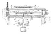
- the chamber 10has an elongated, generally flattened configuration, which in cross section has a generally lenticular shape.
- a lenticular shapehas opposed biconvex surfaces which may have circular curvatures.
- the chambercan have other outer shapes, such as square, rectangular and the like. For instance, a square chamber is disclosed in U.S. Pat. No. 6,143,079, which issued on Nov. 7, 2000, and which is hereby incorporated by reference in its entirety.
- 1–8has an upper wall 12 with an outer convex surface and an inner concave surface, and a lower wall 14 with an outer convex surface and an inner concave surface.
- the walls 12 and 14are connected by vertically short side rails 16 and 18 . These walls and side rails are further joined by an upstream inlet end flange 20 and a downstream outlet end flange 22 . Upstream and downstream relate to the direction of process gas flow, as will be described, and are synonymous in the present description with front and rear.
- both the upper wall 12 and the lower wall 14are thin, curved plate-like elements having a rectangular flat vertical projection.
- the walls 12 and 14desirably have a circular radius of curvature and may be formed by segments cut from a cylindrical tube made of quartz or similar material. In larger chambers, the walls 12 and 14 may be constructed by heating and forming flat quartz plates. Although quartz is preferred, other materials having similar desirable characteristics may be substituted. Some of these desirable characteristics include a high melting point, the ability to withstand large and rapid temperature changes, chemical inertness, and a high transparency to light.
- each side rail 16 , 18may be machined from a quartz rod of rectangular cross section or otherwise formed into the cross sectional shape illustrated in FIG. 2 . More specifically, each side rail 16 , 18 includes a reinforced main body having an upper surface 24 that forms a continuation of the curved exterior surface of the upper wall 12 , and a lower surface 26 which is curved to form a continuation of the exterior surface of the lower wall 14 .
- the laterally exterior surface 28 of each side rail 16 , 18is flat and extends vertically.
- the interior surface of each side rail 16 , 18is formed with longitudinally extending upper and lower recesses 30 a , 30 b that create upper, middle and lower stub wall segments 32 a , 32 b , 32 c , respectively.
- the upper and lower stub wall segments 32 a , 32 cmate with the side edges of the upper and lower walls 12 and 14 at longitudinal weld joints 39 .
- the main body of the side rails 16 , 18has a thickness or width dimension of about 20 mm and a height of about 21 mm.
- a support or stringerpreferably is provided in the form of a flat, rectangular plate 40 that extends between the side rails 16 and 18 .
- the support plate 40includes an aperture 42 defining a void or opening 44 extending across the width of the chamber 10 and dividing the support plate 40 into an inlet section 46 a and an outlet section 46 b .
- the inlet section 46 aextends from the inlet flange 20 to an upstream edge of the opening 44
- the outlet section 46 bextends from a downstream edge of the opening 44 to the outlet flange 22 .
- the inlet section 46 a of the support plateis shorter in the longitudinal direction than is the outlet section 46 b . More specifically, in a preferred arrangement, the inlet section is about 70% of the length of the outlet section. That proportional arrangement generally relates to the process gas flow through the chamber.
- each of the side rails 16 and 18includes the inwardly extending central stub wall 32 b that in effect forms an extension of the support plate 40 .
- the support plate 40in practice terminates at the main body of the side rails 16 , 18 , or, in other words, at the laterally outer extent of the recesses 30 a , 30 b .
- Longitudinal joints 48indicate the welded connection between the lateral edges of the support plate 40 and the central stub walls 32 b of each of the side rails 16 and 18 .
- the central stub walls 32 bprecisely bisect the upper and lower walls 12 and 14 , and the support plate 40 thus lies on the exact centerline or center plane therebetween.
- each of the end flanges 20 , 22comprise outer, generally rectangular slabs 50 , 51 , respectively, having chamfered corners 52 and inner lenticular shaped extensions 54 .
- the inner extensions 54conform to the shapes of the upper and lower walls 12 , 14 and the central support plate 40 . More particularly, short longitudinal portions extend from the slabs 50 , 51 to join with each of these plate-like members 12 , 14 , 40 .
- curvilinear weld joints 56are formed between the curved upper and lower walls 12 , 14 and the upper and lower portions of the extensions 54 , while linear joint lines 58 are defined between central portions of the extensions 54 and the longitudinal ends of the support plate 40 .
- the slab 50 of the inlet flange 20includes a laterally extending aperture 60 (see FIG. 3 ) in an upper portion which leads into an upper region 66 (see FIG. 2 ) within the chamber 10 above the support plate 40 and below the upper wall 12 .
- the slab 51 of the outlet flange 22in contrast, includes a pair of laterally extending apertures 62 , 64 (see FIG. 3 ); the upper aperture 62 communicates with the upper region 66 (see FIG. 2 ) of the chamber 10 previously described, while the lower aperture 64 communicates with a lower region 68 (see FIG. 2 ) of the chamber 10 defined below the support plate 40 and above the lower wall 14 .
- the rounded recesses 30 a , 30 b in the side rails 16 , 18define lateral boundaries of the upper and lower regions 66 , 68 . As will be described below, the wafer processing is done in the upper region 66 only, with the support plate 40 defining the lower boundary of the process zone.
- the opening 44 in the support plate 40is dimensioned to receive a susceptor 70 , as illustrated in FIGS. 3 and 8 , and a temperature compensation ring 72 (see FIGS. 4 and 8 ), which surrounds the susceptor 70 .
- the temperature compensation ring 72has a thermal mass configured to help increase temperature uniformity in the chamber.
- the ringitself is asymmetric relative to a wafer being processed, such that the ring has a different center of thermal mass than the wafer or an uneven distribution of thermal mass about the wafer.
- the ringcan have a substantially rectangular outer perimeter that results in high thermal mass concentrations at the corners but a similar center of thermal mass relative to the wafer.
- the ringcan have an off-center configuration (e.g., the illustrated elongated rectangle) in which the distribution of thermal mass about the wafer is uneven.
- the ringcan receive the wafer in a location other than its center.
- the ringcan be triangular, circular, elliptical, or any other suitable shape, depending in part upon the geometry of other features in the chamber and the gas flow path.
- the susceptor 70is adapted to rotate within the stationary ring 72 and is preferably spaced therefrom across a small annular gap G of about 0.5 to 1.0 mm.
- the centerline of a generally circular temperature compensation ring 72is schematically illustrated in FIG. 4 by the broken line circle 74 shown therein.
- the shape of the aperture 42 in the support plate 40 surrounding the ring 72can also be made circular so that the edges of the opening 44 would be in close proximity to the ring. However, it has been found that somewhat of a rectangular aperture 42 having rounded corners, as shown in FIG. 4 , is preferred.
- the support plate sections 46 a , 46 bmay be cut to provide those exact shapes; or for manufacturing convenience, short, somewhat triangular sections 76 of fill, shown in FIG. 4 , may be welded to the plate sections and the chamber side rails 16 , 18 to provide the desired configuration.
- the circle 74 shown in FIG. 4which represents the centerline of the temperature compensation ring 72 (see FIG. 8 ), is neither centrally positioned with respect to the upstream and downstream ends of the chamber, nor with respect to opening 44 . Instead, the upstream or leading edge of the circle 74 is closer to the downstream edge of the inlet plate section 46 a than is the downstream or trailing edge of the circle to the upstream edge of the outlet plate section 46 b .
- This arrangementhelps maintain the strength of the chamber by reducing the rate of devitrification of the upstream edge of the outlet plate section 46 b . That is, the gas flow heats up as it passes over the susceptor so that the temperature in the chamber walls tends to be the greatest just downstream from the susceptor.
- the upstream edgecan therefore be exposed to significant thermal cycling and devitrification if too close to the susceptor, and thus the susceptor is offset forwardly within the opening 44 to increase the spacing therebetween.
- the offset arrangement discussed directly abovealso affects the flow of the process gases through the chamber. More particularly, the wafer placed upon the susceptor which is surrounded by the ring is positioned close to the downstream edge of the inlet plate section 46 a to minimize the amount of reaction gases which pass through the opening 44 upstream of the wafer. This minimizes the amount of reaction gas which can deposit underneath the susceptor in the lower portion 68 of the chamber 10 . It also should be noted that this configuration increases the difficulty in obtaining a uniform temperature region proximate the wafer.
- the temperature compensation ring 72is supported by three elbow-shaped support elements having vertically extending portions being welded to the support plate sections. More specifically, a front support element or finger 80 is welded to the rear of the front plate section 46 a midway between the rails 16 , 18 of the chamber, and the horizontal portion of the finger or element 80 extends rearwardly into the opening 44 so as to be positioned under the leading edge of the temperature compensation ring 72 . A pair of spaced elements or fingers 82 have elongated horizontal portions that extend forwardly beneath the trailing edge of the compensation ring 72 as seen in FIG. 8 , as well as FIGS. 2–7 .
- each of the fingers or elements 80 , 82includes a pin (not shown) that underlies the compensation ring 72 .
- the compensation ring 72is thus supported in a horizontal plane at three points by upstanding pins (not shown) in the fingers or elements 80 , 82 .
- the pinsmay eventually deteriorate from repeated thermal cycling and exposure to process etch gases, but they can be replaced fairly readily.
- a susceptor 70is shown supported on arms 86 of a suitable support 88 connected to the upper end of a rotatable shaft 90 that extends through a tube 92 depending from the bottom wall of the chamber.
- the susceptor 70is shown approximately level with the upper edge of the ring 72 and with the upper surface of the support plate 40 . This enables a wafer to be positioned above the susceptor 70 and in the upper portion 66 of the process chamber 10 .
- the inlet flange 20is adapted to be connected to an inlet component 94 having a horizontally elongated slot 96 through which a wafer may be inserted, and having an elongated inlet 98 for introducing process gas into the upper portion 66 of the chamber after an isolation valve leading from the slot 96 to a wafer handling chamber (not shown) has been closed.
- the outlet flange 22is adapted to mate with an outlet component 100 for exhausting process gas 112 from the chamber 10 , as well as applying a vacuum to the chamber.
- the outlet flange 22is open to the lower portion 68 of the chamber beneath the support plate as well as the portion 66 above the support plate.
- thermocouples 102extends through the outlet component 100 and into the lower portion 68 of the process chamber.
- the thermocouples 102extend into proximity of the susceptor 70 to sense the local temperature surrounding the susceptor 70 and wafer positioned there above.
- the advantageous positioning of the sensing ends of the thermocouples 102 surrounding the susceptor 70allows comprehensive feedback regarding the temperature of the wafer and enables adjustment of radiant light emitting diode (LED) heat lamp arrays 108 , which will be described later, to compensate for temperature irregularities.
- LEDradiant light emitting diode
- thermocouple 104terminates proximate the front end of the susceptor 70
- a trailing edge thermocouple 106terminates proximate a rear edge of the susceptor
- a lateral thermocouple(not shown) terminates proximate a lateral edge of the susceptor.
- Each of the thermocouples 102enters the temperature compensation ring 72 which is formed of two parts to provide a hollow interior therein. Again, this ring has been described previously in U.S. Pat. No. 6,093,252, which is hereby expressly incorporated by reference.
- the temperature compensation ring 72is constructed of graphite or other such high heat absorbency material.
- the ring 72provides several advantages in the processing environment, primarily reducing edge heat losses from the susceptor 70 . More specifically, the ring 72 closely surrounds the edge of the susceptor 70 and is maintained at a similar temperature during processing, as the materials are similar. The susceptor and ring thus radiate heat toward one another to greatly reduce any radiant losses therebetween.
- Another advantage of the temperature compensation ring 72is preheating and postheating of the reactant gas in the region of the wafer. Specifically, the reactant gas enters the chamber at an ambient, non-reacting temperature and is heated to a temperature suitable for deposition as it passes over the susceptor and wafer.
- the surrounding temperature compensation ring 72thus preheats the reactant gas stream before it reaches the leading edge of the susceptor, and, subsequently, the leading edge of the wafer.
- the process gasthus reaches an approximately steady state temperature before traveling over the edge of the wafer. Additionally, the temperature of the gas does not significantly drop off after passing the downstream edge of the wafer as the temperature compensation ring 72 extends the downstream heating region.
- the ringmay be elongated in a downstream direction such that the temperature drop occurs further downstream from the wafer.
- the gas flow through the chamberis shown in FIG. 8 .
- Reactant gasenters through the inlet component 94 with a predetermined lateral velocity profile, such as the profile described in U.S. Pat. No. 5,221,556, the entirety of which is hereby expressly incorporated by reference.
- the predetermined velocity profileprovides a larger gas flow towards the central portion of the reaction chamber 10 than the laterally outer edges to compensate for the longer deposition travel path over the center of the circular wafer supported on the susceptor 70 . In other words, a greater amount of reactant gas is provided over the central portion of the wafer due to reactant depletion along that flow path over the wafer.
- the reactant gascontinues longitudinally rearward as indicated by arrow 112 and exits through the outlet component 100 and downward through exhaust conduits 114 , as indicated with arrow 116 .
- purge gasis supplied upward through the hollow tube 92 surrounding the shaft 90 , the tube being sized to provide a gas passage surrounding the shaft.
- the purge gasenters the lower portion 68 of the chamber 10 as indicated by arrows 118 .
- the purge gasprevents unwanted deposition of particulates underneath the susceptor 70 and exits through the lower longitudinal aperture 64 in the outlet flange 22 , as indicated by arrow 120 .
- the purge gasthen mixes with the spent reaction gas and continues down along the path of arrow 116 through the exhaust conduits 114 .
- the end flanges 20 , 22are preferably translucent and fabricated from quartz having nitrogen bubbles dispersed therein.
- the central thin walls 12 , 14 and support plate 40are transparent to radiant energy, allowing radiant heating of the susceptor and wafer in the chamber 10 , without creating high temperatures in these structures.
- the translucent flanges 20 , 22scatter radiant energy to reduce “light-piping” therethrough. This protects 0 -rings 122 outside of the flanges 20 , 22 from exposure to extreme temperatures generated within the chamber 10 .
- a section of the tube 92 below the lower wall 14is similarly translucent from nitrogen bubbles dispersed therein.
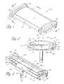
- FIG. 9illustrates a particular arrangement of components surrounding a reaction chamber 130 that can be used for CVD processing.
- Reaction chamber 130is similar to the chamber 10 described with reference to FIGS. 1–8 .
- the chamber 130includes an inner support plate 132 which is similar to the inner support plate 40 as previously described, and thus includes an aperture 133 formed therein.
- the aperture 133is sized to receive a temperature compensation ring 155 and a susceptor 134 for supporting a semiconductor wafer.
- the support plate 132is divided into a front section 135 a upstream of the aperture 133 and a rear section 135 b downstream of the aperture 133 .
- the susceptor 134is positioned on a plurality of radially extending arms 136 of a central hub 138 mounted on a hollow shaft 140 .
- the shaft 140is rotated by a motor 142 disposed below the chamber 130 .
- the rotational coupling between the motor 142 and the shaft 140is explicitly described in U.S. Pat. No. 6,093,252, previously incorporated by reference.
- the motor 142preferably is mounted on a fixed frame and includes adjustment mechanisms for properly positioning the susceptor 134 within the chamber 130 .
- At least one LED heat lamp arrayis arranged around the reaction chamber 130 to heat the susceptor 134 and any wafer thereon.
- a first array of upper LED lamps 146is arranged above the chamber 130 .
- a second lower array of LED lamps 148is arranged below the chamber 130 .
- the at least one LED heat lamp arraycomprises a single LED lamp configured to heat the susceptor 134 and the wafer.
- the second lower array of LED lamps 148may or may not be aligned with the first array of upper LED lamps 146 .
- the distribution of the upper array of LED lamps 146is unimpeded so that a regular sequence of LED lamps is provided across the surface of the chamber 130 .
- the lower array of LED lamps 140is provided across the surface of the chamber 130 except in the region of the shaft 140 .
- one or more spot lights or directed lamps 150are positioned under the chamber 130 and surround a downwardly extending quartz tube 152 formed integrally with the chamber 130 .
- the tube 152concentrically receives the shaft 140 .
- the tube 152 and shaft 140create an annular space therebetween which is used to inject a purge gas into a region underneath the susceptor 134 .
- the directed lamps 150radiate energy to the underside of the susceptor 134 , which may be shadowed by the shaft 152 and supporting structure.
- the specific heating arrangement for the directed lamps 150is similar to that described and illustrated in U.S. Pat. No. 4,836,138, which is hereby expressly incorporated by reference.
- the upper and lower arrays of LED lamps 146 , 148are distributed in a generally rectangular configuration above and below, respectively, the susceptor region 134 . This arrangement, in combination with the directed lamps 150 , focuses the radiant energy on the susceptor 134 and the associated wafer. Different arrangements and locations of the upper and lower arrays of LED lamps can be used. For example, the upper and/or lower arrays of LED lamps could be arranged in a concave fashion.
- the orientation of the upper and lower arrays of LED lamps 146 , 148 with respect to one anotherfurther enhances uniformity of heating of the susceptor 134 .
- the LED lamps 146 , 148can receive the same power levels or receive differing power levels to account for end effects and other phenomena that can vary the temperature gradient across the wafer.
- a configuration for supplying the differing power levels to the LED lamps 146 , 148is described with reference to FIG. 13 .
- FIG. 9An enlarged temperature compensation ring 155 is shown in FIG. 9 . It should be noted, however, that the peripheral shape of the modified temperature compensation ring 155 is generally rectangular and the shape generally conforms to the radiant heat from the upper and lower arrays of LED lamps 146 , 148 . This arrangement is highly efficient and results in more uniform temperatures across the susceptor 134 .
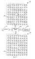
- a typical grid of LED heat lampswhich is fashioned from the bottom array of LED lamps 148 , is illustrated therein.
- a wafer(not shown) is located on the susceptor 134 and within the chamber 130 .
- the waferrests on the susceptor 134 and is positioned generally above the bottom array of LED lamps 148 .
- the reactant gas flow direction 170 through the chamber 130is also shown. It should be noted that, in some chambers, the top array and the bottom array can be constructed differently.
- the bottom array of LED lamps 148includes light emitting diode (LED) lamps 180 .
- the LED lamps 180are located below the susceptor and are spread across the grid.
- the bottom array 148also accommodates the spot lamps 150 , the rotating shaft 140 and the gas supply tube 152 (see FIG. 9 ).
- the central region of the bottom array of LED lamps 148does not admit to full LED lamps 180 across its entire surface.
- the top array of LED lamps 146(see FIG. 9 ) would not have such obstructions and full LED lamps across its entire surface are easily accommodated and implemented.
- the arrays of LED lampsare rectangular and approximately ninety LED lamps make up the bottom array of LED lamps.
- the top array of LED lamps 146may include a similar number of LED lamps.
- each square inch of the gridcomprises twenty-five LED lamps.
- the LED lampsare circular in their arrangement with the LEDs arranged in concentric circles. It should be noted that other numbers of LED lamps can be used in the selected arrangement.
- the number of LED lamps in the top gridcan be different than the number of LED lamps in the bottom grid.
- a plurality of the LED lamps from the top or bottom gridcan be physically grouped so as to facilitate their removal and replacement within their respective grid.
- the number of LED lamps in a groupranges from fifty to two hundred and fifty.
- These groupscan be configured as a module that plugs into an underlying base. The base provides electrical contacts.
- the LED lamps 180advantageously reduce temperature gradients within the chamber such that nonuniformities in temperature across a wafer can be reduced or eliminated.
- nonuniformities in temperature within the chamber or nonuniformities across the wafer processed within the chambercan be measured or estimated to determine relative cold spots or hot spots.
- one or more of the LED lamps within the arrayscan be adjusted to provide differential power output across a region of the array.
- the temperature gradient within the chamber and, therefore across the wafercan be greatly reduced and the uniformity of the product can be improved.
- temperature nonuniformitiescan be determined in any suitable manner, including but not limited to, direct temperature measurements of the wafer, indirect temperature measurements (i.e., measuring temperature within the chamber) or measuring the thickness of the processed materials.
- the LED lamps 180operate in response to pre-programming. In this embodiment, the LED lamps vary their heat output over time based on the pre-programming. In another embodiment, a failure of one or more LED lamps 180 is detected and compensated for by operational LED lamps 180 .
- FIG. 12a cross-sectional drawing of a portion of the array 148 with one arrangement of a row of LED lamps is shown.
- the rowcomprises LED lamps 180 ( a )– 180 ( f ) covered by a perforated reflector layer 181 .
- the perforated reflector layer 181is coupled to supports 184 ( a )–( f ).
- the supports 184 ( a )–( f ) and the LED lamps 180 ( a )–( f )are both coupled to a printed circuit board 186 .
- the LED lamps 180 ( a )– 180 ( f )include gallium aluminum arsenide (GaAIA) infrared emitting diodes enclosed in a transparent plastic case.
- GaAIAgallium aluminum arsenide
- types OP290, OP291, and OP292 of diodes manufactured by Optek Technology, Inc. of Carrollton, Tex.can be used.
- Each LED lamp 180is positioned to emit electromagnetic radiation in a focussed beam towards the susceptor 134 (see FIG. 11 ).
- Each LED lamp 180generally comprises two connectors, an anode and a cathode (not shown), disposed at the interface with the PCB 186 . The two connectors extend into the LED lamp 180 and are electrically connected to a diode located therein.
- LED Lamps 180 ( a )–( f )can have varied dimensions depending upon the application and size desired.
- the perforated reflector layer 181is formed of a reflective material with perforations or apertures 182 ( a )–( f ) formed therein.
- the apertures 182 ( a )–( f )substantially align with the LED lamps 180 ( a )–( f ) to permit the electromagnetic radiation emitted by the LED lamps 180 ( a )–( f ) to pass through the reflector layer 181 .
- the shape of the apertures 182 ( a )–( f )can be selected to compliment the irradiance pattern of the LED lamps. For example, a round shape can be selected for embodiments where each of the LED lamps 180 ( a )–( f ) emits electromagnetic radiation along a cylindrical path towards the susceptor.
- the apertures 182 ( a )–( f )can be sized so as to reduce the reflected electromagnetic radiation that impinges upon the LED lamps 180 ( a )–( f ). In this way, the reflector layer 181 reflects electromagnetic radiation that was reflected towards the LED lamps 180 ( a )–( f ).
- the reflector layer 181can comprise, for example, a metallic surface such as gold.
- the perforated reflector layer 181attaches to the supports 184 ( a )–( f ).
- the supports 184 ( a )–( f )provide a barrier between adjacent LED lamps 180 ( a )–( f ).
- the supportscomprise a metallic material, for example, aluminum. Alternatively, steel can be used.
- the printed circuit board (PCB) 186is well known in the art and provides an electrical and mechanical interface for the LED lamps 180 ( a )–( f ).
- the PCB 186also provides the interface to electronic heater control circuitry, described with reference to FIG. 13 .
- the PCB 186further provides an attachment surface for the supports 184 ( a )–( f ).
- one or more PCBsmay be used to attach one or LED lamps thereto.
- FIG. 13is a schematic view of the heating system of the present invention and also shows electrical connections between a suitable control circuit.
- the heating systemcomprises an upper array of LED lamps 146 , a lower array of LED lamps 148 , transmitters 250 , a heater control module 252 , and a temperature control input 254 .
- the upper and lower arrays of LED lampselectrically connect with the heater control module 252 via one or more printed circuit boards (PCB) 186 .
- the heater control modulereceives one or more signal from the transmitters 250 . These signals can represent the temperatures that are measured by the thermocouples 102 .
- the heater control module 252can farther receive signals in the form of temperature settings from the temperature control input 254 . These temperature settings can be indicative of a temperature profile programmed for the operation of the chamber. Alternatively, the desired temperature profile is directly programmed into the heater control module 252 .
- the heater control module 252receives a signal from the upper and lower arrays of LED lamps 146 , 148 indicating that one or more LED lamps are not operating properly. This signal can identify, for example, a failed LED lamp, a misaligned LED lamp, and an LED lamp that is performing out of specification.
- the heater control module 252In response to one, or more than one, of these various input signals, the heater control module 252 sends control signals to each LED lamp 180 or groups of LED lamps.
- the control signalsallow the heater control module 252 to dynamically control the output of the LED lamps. In this way, the heater control module 252 can, for example, compensate for a failed LED, vary the output of the LED lamps over time based on a program, and adjust the output of the LED lamps based on feedback from the chamber.
- Each LED lamp in the upper or lower arrays of LED lampscan be operated at different power levels by control signals produced by the heater control module 252 .
- each lampcan be controlled in groups.
- the groups of LED lamps controlled by the heater control module 252can comprise only LED lamps from the top or bottom arrays of LED lamps. In one embodiment, the groups of LED lamps comprise LED lamps from both of the top and bottom arrays of LED lamps.
- each LED lampcan be associated with a temperature control module based on feedback from temperature sensors (e.g., the thermocouples 102 , 104 , 106 of FIG. 8 ).
- the LED heat lamps 180 ( a )–( f )have their connector ends connected with the PCB 186 .
- the LED heat lamps 180 ( a )–( f )are thus controlled individually or as a group by the output signals from the heater control module 252 .
- the LED heat lamps 180 ( a )–( f )are presented as an example to illustrate how one or more LED lamps can be controlled by the heater control module 252 .
- the other LED lamps 180 in the upper and lower arrays of LEDscan be similarly controlled, individually or in groups, by the heater control module 252 .
- the directed lamps 150(see FIG. 9 ) have their respective terminals coupled by conductors (not shown) which are in turn coupled to receive the control signals from the heater control module 252 .
- each of the directed lamps 150operates in unison to provide a concentrated heat energy receiving zone at the center area of the susceptor 134 .
- the heater control module 252When an input signal is received from the temperature control input 254 to indicate the start of a deposition cycle, the heater control module 252 responds by applying full power to the directed lamps 150 , to the selected LED lamps 180 of the upper array of LED lamps 146 , and to the selected LED lamps 180 of the lower array of LED lamps 148 . That same input signal contains information indicative of a desired operating temperature at which the deposition cycle is to be accomplished.
- the application of full power to the directed lamps 150 and to the selected LED lamps of the upper and lower arrays of LED lamps 146 , 148produces a rapid rise in the temperature in the central area of the susceptor 134 , and of course, in the central area of the wafer being processed.
- a master temperature sensorlocated within the shaft 152 senses the rapid rise in temperature and sends signals indicative thereof to the electronic heater control circuitry 152 .
- the electronic heater control circuitry 152compares the sensed temperature with the desired operating temperature and adjusts the power supplied to the directed lamps 150 and the selected LED lamps of the upper and lower arrays of LED lamps to produce and maintain the desired operating temperature in the central area of the susceptor 134 and wafer.
- the temperatures about the periphery of the susceptor 134 and in the temperature compensation ring 72are simultaneously being brought up to temperature by the selected LED lamps of the upper and lower arrays of LED lamps.
- the increasing temperatures in the peripherally located heating zones or regionsare sensed by the thermocouples 104 and additional sensors if desired.
- the thermocouplesproduce signals indicative of the sensed temperatures to the transmitters 250 .
- the transmitters 250provide these signals to the heater control module 252 .
- the signals received by the heater control module 252 from the transmitters 250are compared with the signal received from the master temperature sensor to adjust the power to the selected LED lamps to bring the temperatures in the peripherally located heating zones into alignment with the temperature in the central area of the susceptor 134 and the wafer.
- the LED heating lamps 180may be ideally set to normally operate at temperatures which are offset, i.e. different than the desired operating temperature in the central area of the wafer and the susceptor 134 . And, the process of sensing temperatures and adjusting the power applied to the various groups, or banks of LED heating elements as needed, is continued throughout the deposition cycle. The object of all this is, of course to provide a uniform, or flat temperature gradient in all of the relevant areas of the substrate, susceptor and temperature compensation ring throughout the deposition cycles.
- the power applied to the directed lamps 150 and the selected LED heating lamps proximate the center of the upper and lower arrays of LED lampsis reduced and the temperature in the peripherally located heating region will follow along with the reduction of heat at the center areas of the wafer and the susceptor 134 .
- modulemeans, but is not limited to, a software or hardware component, such as a processor, FPGA, or ASIC, which performs certain tasks.
- a modulemay advantageously be configured to reside on the addressable storage medium and configured to execute on one or more processors.
- a modulemay include, by way of example, components, such as software components, object-oriented software components, class components and task components, processes, functions, attributes, procedures, subroutines, segments of program code, drivers, firmware, microcode, circuitry, data, databases, data structures, tables, arrays, and variables.
- componentssuch as software components, object-oriented software components, class components and task components, processes, functions, attributes, procedures, subroutines, segments of program code, drivers, firmware, microcode, circuitry, data, databases, data structures, tables, arrays, and variables.
- the functionality provided for in the components and modulesmay be combined into fewer components and modules or further separated into additional components and modules. Additionally, the components and modules may advantageously be implemented to execute on one or more computers.
Landscapes
- Engineering & Computer Science (AREA)
- Chemical & Material Sciences (AREA)
- Toxicology (AREA)
- Health & Medical Sciences (AREA)
- Mechanical Engineering (AREA)
- General Engineering & Computer Science (AREA)
- Condensed Matter Physics & Semiconductors (AREA)
- Chemical Kinetics & Catalysis (AREA)
- Metallurgy (AREA)
- Organic Chemistry (AREA)
- General Chemical & Material Sciences (AREA)
- Physics & Mathematics (AREA)
- Materials Engineering (AREA)
- General Physics & Mathematics (AREA)
- Manufacturing & Machinery (AREA)
- Computer Hardware Design (AREA)
- Microelectronics & Electronic Packaging (AREA)
- Power Engineering (AREA)
- Chemical Vapour Deposition (AREA)
- Waste-Gas Treatment And Other Accessory Devices For Furnaces (AREA)
- Furnace Details (AREA)
Abstract
Description
This application is a continuation of application Ser. No. 10/217,230, filed Aug. 9, 2002, now U.S. Pat. No. 6,818,864 and titled LED HEAT LAMP ARRAYS FOR CVD HEATING, which is hereby incorporated by reference in its entirety.
1. Field of the Invention
The present invention generally relates to heat lamps. More specifically, the present invention relates to heat lamps for improving the temperature uniformity in a field heated by one or more LED heat lamps.
2. Related Art
Chemical vapor deposition (CVD) is a very well known process in the semiconductor industry for forming thin films of materials on substrates, such as silicon wafers. In a CVD process, gaseous molecules of the material to be deposited are supplied to wafers to form a thin film of that material on the wafers by chemical reaction. Such formed thin films may be polycrystalline, amorphous or epitaxial. Typically, CVD processes are conducted at the elevated temperatures to accelerate the chemical reaction and to produce high quality films. Some processes, such as epitaxial silicon deposition, are conducted at extremely high temperatures (>900° C.).
To achieve the desired high temperatures, substrates can be heated using resistance heating, induction heating or radiant heating. Among these heating techniques, radiant heating is the most efficient technique and, hence, is the currently favored method for certain types of CVD. Radiant heating involves positioning infrared lamps around a reaction chamber positioned within high-temperature ovens, called reactors. Unfortunately, radiant energy has a tendency to create nonuniform temperature distributions, including “hot spots,” due to the use of localized radiant energy sources and consequent focusing and interference effects.
During a CVD process, one or more substrates are placed on a wafer support (i.e., susceptor) inside a chamber defined within the reactor (i.e., the reaction chamber). Both the wafer and the support are heated to a desired temperature. In a typical wafer treatment step, reactant gases are passed over the heated wafer, causing chemical vapor deposition (CVD) of a thin layer of the desired material on the wafer. If the deposited layer has the same crystallographic structure as the underlying silicon wafer, it is called an epitaxial layer. This is also sometimes called a monocrystalline layer because it has only one crystal structure. Through subsequent processes, these layers are made into integrated circuits, producing from tens to thousands or even millions of integrated devices, depending on the size of the wafer and the complexity of the circuits.
Various process parameters must be carefully controlled to ensure a high quality of layers resulting from CVD. One such critical parameter is the temperature of the wafer during each treatment step of wafer processing. During CVD, for example, the wafer temperature dictates the rate of material deposition on the wafer because the deposition gases react at particular temperatures and deposit on the wafer. If the temperature varies across the surface of the wafer, uneven deposition of the film occurs and the physical properties will not be uniform over the wafer. Furthermore, in epitaxial deposition, even slight temperature non-uniformity can result in crystallographic slip.
In the semiconductor industry, it is important that the material be deposited uniformly thick with uniform properties over the wafer. For instance, in Very Large and Ultra Large Scale Integrated Circuit (VLSI and ULSI) technologies, the wafer is divided into individual chips having integrated circuits thereon. If a CVD process step produces deposited layers with nonuniformities, devices at different areas on the chips may have inconsistent operation characteristics or may fail altogether.
The systems and methods of the present invention have several features, no single one of which are solely responsible for its desirable attributes. Without limiting the scope of this invention as expressed by the claims which follow, its more prominent features will now be discussed briefly. After considering this discussion, and particularly after reading the section entitled “Detailed Description of the Preferred Embodiments,” one will understand how the features of this invention provide several advantages over traditional CVD heating methods and systems.
One aspect is a chemical vapor deposition apparatus that comprises a high temperature processing chamber and a susceptor disposed within the chamber for supporting a wafer to be processed, the susceptor comprising a top surface, a bottom surface, and a perimeter. The apparatus further comprises a plurality of light emitting diodes (LEDs) located on a surface of the chamber, each configured to emit radiant energy towards the top surface, and a controller configured to adjust the radiant energy emitted by at least one of the plurality of LEDs relative to another one of the plurality of LEDs.
Another aspect is a method of processing a semiconductor in a chamber by applying heat from an array of LED lamps disposed adjacent to the chamber, each LED lamp being configured to emit directional radiant energy towards a substrate in the chamber. The method comprises inserting a wafer in a chamber, sensing an operational status of a plurality of LED lamps, if an LED from the plurality of LED lamps is non-operational, then adjusting a planned temperature profile for the plurality of LED lamps to compensate for the non-operational LED lamp. The method further includes applying heat from the plurality of LED lamps to the wafer, identifying nonuniformities in the temperature of the wafer, and adjusting an energy level output of at least one of the plurality of LED lamps with respect to another one of the plurality of LED lamps to compensate for the nonuniformity.
Still another aspect is a semiconductor processing apparatus that comprises a chamber defined by at least one wall, a structure for supporting a substrate within the chamber, and at least one LED heat lamp array disposed proximate to the chamber.
Yet another aspect is an apparatus for processing semiconductor wafers at elevated temperatures that comprises a high temperature processing chamber defined by at least one wall, a susceptor disposed within the chamber for supporting a wafer to be processed, the susceptor comprising a top surface, a bottom surface, a perimeter, a first array of LED heat lamps being disposed proximate to the susceptor, and at least one LED lamp of the first array of LED heat lamps configured to emit directional radiant energy in a first direction towards the top surface. The apparatus further comprises a first perforated reflector located between the first array of LED heat lamps and the susceptor, the perforations being aligned with the at least one LED lamp of the first array and a second array of LED heat lamps being disposed proximate to the susceptor and parallel to the first array of LED heat lamps, the susceptor being disposed between at least a portion of the first array of LED heat lamps and said second array of LED heat lamps. The apparatus still further comprises at least one LED lamp of the second array of LED heat lamps configured to emit directional radiant energy in a second direction towards the bottom surface, both of the directions being at least partially disposed within a volume defined by the susceptor perimeter in a direction normal to the susceptor, and a second perforated reflector located between the second array of LED heat lamps and the susceptor, the perforations being aligned with the at least one LED lamp of the second array.
Another aspect is a chemical vapor deposition apparatus that comprises a process chamber having an area for horizontal positioning of a substrate within a substrate treatment zone and having chamber walls for conducting a flow of gas across a surface of the substrate, a first two-dimensional array of heat lamps being disposed generally above the substrate treatment zone, each LED of the first two-dimensional array of heat lamps having a length and a width so that the first two-dimensional array of heat lamps spans the substrate treatment zone in a first row and spans the substrate treatment zone in a first column generally perpendicular to the first row. The apparatus further comprises a first perforated reflector located between the first two-dimensional array of heat lamps and the substrate, the perforations being substantially aligned with the first two-dimensional array of heat lamps, a second two-dimensional array of heat lamps being disposed generally below said substrate treatment zone, each LED of the second two-dimensional array of heat lamps having a length and a width so that the second two-dimensional array of heat lamps spans the substrate treatment zone in a second row and spans the substrate treatment zone in a second column, at least one LED from the second row or second column having means for adjusting energy lamp output relative to another of the LEDs from the same second row or column, and a second perforated reflector located between the second two-dimensional array of heat lamps and the substrate, the perforations being substantially aligned with the second two-dimensional array of heat lamps.
Still another aspect is a method of processing a substrate in a chamber by applying heat from an LED lamp disposed adjacent to the chamber, the LED lamp being configured to emit directional radiant energy towards the substrate. The method comprises inserting a wafer in a chamber, applying heat from the LED lamp to the wafer, identifying nonuniformities in the temperature of the wafer, and adjusting an energy level output of the LED lamp to compensate for the nonuniformity.
These and other features, aspects and advantages of the present invention will now be described with reference to the drawings of several preferred embodiments, which embodiments are intended to illustrate and not to limit the invention.
U.S. Pat. No. 4,836,138, which issued on Jun. 6, 1989 to Robinson et al., and U.S. Pat. No. 4,828,224, which issued on May 9, 1989 to Crabb et al., both of which are hereby expressly incorporated by reference, described exemplary cold-wall single wafer reaction chambers. These reaction chambers are exemplary environments that can be modified according to the teachings of this patent. For example, LED heat lamps and arrays of LED heat lamps can be used in accordance with certain features, aspects and advantages of the present invention. In one preferred arrangement, the LED heat lamps and arrays are used in CVD chambers. In a more preferred arrangement, the LED heat lamps are used in CVD chambers that have been optimized for epitaxial deposition.
U.S. Pat. No. 6,093,252, which issued on Jul. 25, 2000 to Wengert et al., also disclosed a reaction chamber configuration that can be modified to use LED heat lamps and arrays of LED heat lamps having certain features, aspects and advantages in accordance with the present invention. The disclosure of that patent is hereby expressly incorporated by reference.
With reference now toFIGS. 1–8 , anexemplary reactor chamber 10 for chemical vapor processing and the like is illustrated. As can be seen, thechamber 10 has an elongated, generally flattened configuration, which in cross section has a generally lenticular shape. A lenticular shape has opposed biconvex surfaces which may have circular curvatures. In some configurations, the chamber can have other outer shapes, such as square, rectangular and the like. For instance, a square chamber is disclosed in U.S. Pat. No. 6,143,079, which issued on Nov. 7, 2000, and which is hereby incorporated by reference in its entirety. The illustrated chamber ofFIGS. 1–8 has anupper wall 12 with an outer convex surface and an inner concave surface, and alower wall 14 with an outer convex surface and an inner concave surface. Thewalls inlet end flange 20 and a downstreamoutlet end flange 22. Upstream and downstream relate to the direction of process gas flow, as will be described, and are synonymous in the present description with front and rear.
With reference now toFIG. 2 , both theupper wall 12 and thelower wall 14 are thin, curved plate-like elements having a rectangular flat vertical projection. Thewalls walls
The thick side rails16,18 may be machined from a quartz rod of rectangular cross section or otherwise formed into the cross sectional shape illustrated inFIG. 2 . More specifically, eachside rail upper surface 24 that forms a continuation of the curved exterior surface of theupper wall 12, and alower surface 26 which is curved to form a continuation of the exterior surface of thelower wall 14. The laterallyexterior surface 28 of eachside rail side rail lower recesses 30a,30bthat create upper, middle and lowerstub wall segments stub wall segments 32a,32cmate with the side edges of the upper andlower walls
In the illustrated arrangement, a support or stringer preferably is provided in the form of a flat,rectangular plate 40 that extends between the side rails16 and18. As seen inFIG. 4 , thesupport plate 40 includes anaperture 42 defining a void oropening 44 extending across the width of thechamber 10 and dividing thesupport plate 40 into an inlet section46aand anoutlet section 46b. The inlet section46aextends from theinlet flange 20 to an upstream edge of theopening 44, and theoutlet section 46bextends from a downstream edge of theopening 44 to theoutlet flange 22. As may be seen fromFIG. 4 , the inlet section46aof the support plate is shorter in the longitudinal direction than is theoutlet section 46b. More specifically, in a preferred arrangement, the inlet section is about 70% of the length of the outlet section. That proportional arrangement generally relates to the process gas flow through the chamber.
As best seen inFIG. 2 , each of the side rails16 and18 includes the inwardly extendingcentral stub wall 32bthat in effect forms an extension of thesupport plate 40. In this respect, thesupport plate 40 in practice terminates at the main body of the side rails16,18, or, in other words, at the laterally outer extent of therecesses 30a,30b.Longitudinal joints 48 indicate the welded connection between the lateral edges of thesupport plate 40 and thecentral stub walls 32bof each of the side rails16 and18. Thecentral stub walls 32bprecisely bisect the upper andlower walls support plate 40 thus lies on the exact centerline or center plane therebetween.
With reference toFIGS. 1 and 3 , each of theend flanges rectangular slabs corners 52 and inner lenticular shapedextensions 54. With reference now toFIGS. 1 and 3 , theinner extensions 54 conform to the shapes of the upper andlower walls central support plate 40. More particularly, short longitudinal portions extend from theslabs like members chamber 10, curvilinear weld joints56 are formed between the curved upper andlower walls extensions 54, while linearjoint lines 58 are defined between central portions of theextensions 54 and the longitudinal ends of thesupport plate 40.
Theslab 50 of theinlet flange 20 includes a laterally extending aperture60 (seeFIG. 3 ) in an upper portion which leads into an upper region66 (seeFIG. 2 ) within thechamber 10 above thesupport plate 40 and below theupper wall 12. Theslab 51 of theoutlet flange 22, in contrast, includes a pair of laterally extendingapertures 62,64 (seeFIG. 3 ); theupper aperture 62 communicates with the upper region66 (seeFIG. 2 ) of thechamber 10 previously described, while thelower aperture 64 communicates with a lower region68 (seeFIG. 2 ) of thechamber 10 defined below thesupport plate 40 and above thelower wall 14. The rounded recesses30a,30bin the side rails16,18 define lateral boundaries of the upper andlower regions upper region 66 only, with thesupport plate 40 defining the lower boundary of the process zone.
Theopening 44 in thesupport plate 40 is dimensioned to receive asusceptor 70, as illustrated inFIGS. 3 and 8 , and a temperature compensation ring72 (seeFIGS. 4 and 8 ), which surrounds thesusceptor 70. Thetemperature compensation ring 72 has a thermal mass configured to help increase temperature uniformity in the chamber. In one configuration, the ring itself is asymmetric relative to a wafer being processed, such that the ring has a different center of thermal mass than the wafer or an uneven distribution of thermal mass about the wafer. For instance, in one arrangement, the ring can have a substantially rectangular outer perimeter that results in high thermal mass concentrations at the corners but a similar center of thermal mass relative to the wafer. In other arrangements, the ring can have an off-center configuration (e.g., the illustrated elongated rectangle) in which the distribution of thermal mass about the wafer is uneven. For instance, the ring can receive the wafer in a location other than its center. Of course, the ring can be triangular, circular, elliptical, or any other suitable shape, depending in part upon the geometry of other features in the chamber and the gas flow path.
Thesusceptor 70 is adapted to rotate within thestationary ring 72 and is preferably spaced therefrom across a small annular gap G of about 0.5 to 1.0 mm. The centerline of a generally circulartemperature compensation ring 72 is schematically illustrated inFIG. 4 by thebroken line circle 74 shown therein. The shape of theaperture 42 in thesupport plate 40 surrounding thering 72 can also be made circular so that the edges of theopening 44 would be in close proximity to the ring. However, it has been found that somewhat of arectangular aperture 42 having rounded corners, as shown inFIG. 4 , is preferred. Thesupport plate sections 46a,46bmay be cut to provide those exact shapes; or for manufacturing convenience, short, somewhattriangular sections 76 of fill, shown inFIG. 4 , may be welded to the plate sections and the chamber side rails16,18 to provide the desired configuration.
It will be noted that thecircle 74 shown inFIG. 4 , which represents the centerline of the temperature compensation ring72 (seeFIG. 8 ), is neither centrally positioned with respect to the upstream and downstream ends of the chamber, nor with respect toopening 44. Instead, the upstream or leading edge of thecircle 74 is closer to the downstream edge of the inlet plate section46athan is the downstream or trailing edge of the circle to the upstream edge of theoutlet plate section 46b. This arrangement helps maintain the strength of the chamber by reducing the rate of devitrification of the upstream edge of theoutlet plate section 46b. That is, the gas flow heats up as it passes over the susceptor so that the temperature in the chamber walls tends to be the greatest just downstream from the susceptor. The upstream edge can therefore be exposed to significant thermal cycling and devitrification if too close to the susceptor, and thus the susceptor is offset forwardly within theopening 44 to increase the spacing therebetween.
In some configurations, the offset arrangement discussed directly above also affects the flow of the process gases through the chamber. More particularly, the wafer placed upon the susceptor which is surrounded by the ring is positioned close to the downstream edge of the inlet plate section46ato minimize the amount of reaction gases which pass through theopening 44 upstream of the wafer. This minimizes the amount of reaction gas which can deposit underneath the susceptor in thelower portion 68 of thechamber 10. It also should be noted that this configuration increases the difficulty in obtaining a uniform temperature region proximate the wafer.
With continued reference toFIGS. 4 and 8 , thetemperature compensation ring 72 is supported by three elbow-shaped support elements having vertically extending portions being welded to the support plate sections. More specifically, a front support element orfinger 80 is welded to the rear of the front plate section46amidway between therails element 80 extends rearwardly into theopening 44 so as to be positioned under the leading edge of thetemperature compensation ring 72. A pair of spaced elements orfingers 82 have elongated horizontal portions that extend forwardly beneath the trailing edge of thecompensation ring 72 as seen inFIG. 8 , as well asFIGS. 2–7 . Preferably, each of the fingers orelements compensation ring 72. Thecompensation ring 72 is thus supported in a horizontal plane at three points by upstanding pins (not shown) in the fingers orelements
InFIG. 8 , asusceptor 70 is shown supported onarms 86 of asuitable support 88 connected to the upper end of arotatable shaft 90 that extends through atube 92 depending from the bottom wall of the chamber. Thesusceptor 70 is shown approximately level with the upper edge of thering 72 and with the upper surface of thesupport plate 40. This enables a wafer to be positioned above thesusceptor 70 and in theupper portion 66 of theprocess chamber 10.
Still referring toFIG. 8 , theinlet flange 20 is adapted to be connected to aninlet component 94 having a horizontally elongatedslot 96 through which a wafer may be inserted, and having anelongated inlet 98 for introducing process gas into theupper portion 66 of the chamber after an isolation valve leading from theslot 96 to a wafer handling chamber (not shown) has been closed. Correspondingly, theoutlet flange 22 is adapted to mate with anoutlet component 100 for exhaustingprocess gas 112 from thechamber 10, as well as applying a vacuum to the chamber. As can be seen fromFIG. 8 , theoutlet flange 22 is open to thelower portion 68 of the chamber beneath the support plate as well as theportion 66 above the support plate.
A plurality of temperature sensing devices, for example,thermocouples 102, extends through theoutlet component 100 and into thelower portion 68 of the process chamber. Thethermocouples 102 extend into proximity of thesusceptor 70 to sense the local temperature surrounding thesusceptor 70 and wafer positioned there above. As has been described previously in U.S. Pat. No. 6,093,252, the advantageous positioning of the sensing ends of thethermocouples 102 surrounding thesusceptor 70 allows comprehensive feedback regarding the temperature of the wafer and enables adjustment of radiant light emitting diode (LED)heat lamp arrays 108, which will be described later, to compensate for temperature irregularities. More particularly, aleading edge thermocouple 104 terminates proximate the front end of thesusceptor 70, a trailingedge thermocouple 106 terminates proximate a rear edge of the susceptor and a lateral thermocouple (not shown) terminates proximate a lateral edge of the susceptor. Each of thethermocouples 102 enters thetemperature compensation ring 72 which is formed of two parts to provide a hollow interior therein. Again, this ring has been described previously in U.S. Pat. No. 6,093,252, which is hereby expressly incorporated by reference.
Preferably, thetemperature compensation ring 72 is constructed of graphite or other such high heat absorbency material. Thering 72 provides several advantages in the processing environment, primarily reducing edge heat losses from thesusceptor 70. More specifically, thering 72 closely surrounds the edge of thesusceptor 70 and is maintained at a similar temperature during processing, as the materials are similar. The susceptor and ring thus radiate heat toward one another to greatly reduce any radiant losses therebetween. Another advantage of thetemperature compensation ring 72 is preheating and postheating of the reactant gas in the region of the wafer. Specifically, the reactant gas enters the chamber at an ambient, non-reacting temperature and is heated to a temperature suitable for deposition as it passes over the susceptor and wafer. The surroundingtemperature compensation ring 72 thus preheats the reactant gas stream before it reaches the leading edge of the susceptor, and, subsequently, the leading edge of the wafer. The process gas thus reaches an approximately steady state temperature before traveling over the edge of the wafer. Additionally, the temperature of the gas does not significantly drop off after passing the downstream edge of the wafer as thetemperature compensation ring 72 extends the downstream heating region. In some arrangements, the ring may be elongated in a downstream direction such that the temperature drop occurs further downstream from the wafer.
The gas flow through the chamber is shown inFIG. 8 . Reactant gas enters through theinlet component 94 with a predetermined lateral velocity profile, such as the profile described in U.S. Pat. No. 5,221,556, the entirety of which is hereby expressly incorporated by reference. The predetermined velocity profile provides a larger gas flow towards the central portion of thereaction chamber 10 than the laterally outer edges to compensate for the longer deposition travel path over the center of the circular wafer supported on thesusceptor 70. In other words, a greater amount of reactant gas is provided over the central portion of the wafer due to reactant depletion along that flow path over the wafer.
The reactant gas continues longitudinally rearward as indicated byarrow 112 and exits through theoutlet component 100 and downward throughexhaust conduits 114, as indicated witharrow 116. Typically, purge gas is supplied upward through thehollow tube 92 surrounding theshaft 90, the tube being sized to provide a gas passage surrounding the shaft. The purge gas enters thelower portion 68 of thechamber 10 as indicated byarrows 118. The purge gas prevents unwanted deposition of particulates underneath thesusceptor 70 and exits through the lowerlongitudinal aperture 64 in theoutlet flange 22, as indicated byarrow 120. The purge gas then mixes with the spent reaction gas and continues down along the path ofarrow 116 through theexhaust conduits 114.
With reference again toFIGS. 1–7 , theend flanges thin walls support plate 40, on the other hand, are transparent to radiant energy, allowing radiant heating of the susceptor and wafer in thechamber 10, without creating high temperatures in these structures. Thetranslucent flanges rings 122 outside of theflanges chamber 10. Preferably, a section of thetube 92 below thelower wall 14 is similarly translucent from nitrogen bubbles dispersed therein.
At least one LED heat lamp array is arranged around thereaction chamber 130 to heat thesusceptor 134 and any wafer thereon. A first array ofupper LED lamps 146 is arranged above thechamber 130. A second lower array ofLED lamps 148 is arranged below thechamber 130. In another embodiment, the at least one LED heat lamp array comprises a single LED lamp configured to heat thesusceptor 134 and the wafer.
The second lower array ofLED lamps 148 may or may not be aligned with the first array ofupper LED lamps 146. The distribution of the upper array ofLED lamps 146 is unimpeded so that a regular sequence of LED lamps is provided across the surface of thechamber 130. The lower array ofLED lamps 140, on the other hand, is provided across the surface of thechamber 130 except in the region of theshaft 140. Thus, one or more spot lights or directedlamps 150 are positioned under thechamber 130 and surround a downwardly extendingquartz tube 152 formed integrally with thechamber 130. Thetube 152 concentrically receives theshaft 140. Thetube 152 andshaft 140 create an annular space therebetween which is used to inject a purge gas into a region underneath thesusceptor 134. The directedlamps 150 radiate energy to the underside of thesusceptor 134, which may be shadowed by theshaft 152 and supporting structure. The specific heating arrangement for the directedlamps 150 is similar to that described and illustrated in U.S. Pat. No. 4,836,138, which is hereby expressly incorporated by reference.
The upper and lower arrays ofLED lamps susceptor region 134. This arrangement, in combination with the directedlamps 150, focuses the radiant energy on thesusceptor 134 and the associated wafer. Different arrangements and locations of the upper and lower arrays of LED lamps can be used. For example, the upper and/or lower arrays of LED lamps could be arranged in a concave fashion.
The orientation of the upper and lower arrays ofLED lamps susceptor 134. Generally, theLED lamps LED lamps FIG. 13 .
An enlargedtemperature compensation ring 155 is shown inFIG. 9 . It should be noted, however, that the peripheral shape of the modifiedtemperature compensation ring 155 is generally rectangular and the shape generally conforms to the radiant heat from the upper and lower arrays ofLED lamps susceptor 134.
With reference now toFIG. 10 , a typical grid of LED heat lamps, which is fashioned from the bottom array ofLED lamps 148, is illustrated therein. During processing, a wafer (not shown) is located on thesusceptor 134 and within thechamber 130. The wafer rests on thesusceptor 134 and is positioned generally above the bottom array ofLED lamps 148. The reactantgas flow direction 170 through thechamber 130 is also shown. It should be noted that, in some chambers, the top array and the bottom array can be constructed differently.
With reference now toFIG. 11 , the grid shown inFIG. 10 is illustrated with thesusceptor 134 shown by dashed lines. The bottom array ofLED lamps 148 includes light emitting diode (LED)lamps 180. TheLED lamps 180 are located below the susceptor and are spread across the grid. In this arrangement, thebottom array 148 also accommodates thespot lamps 150, therotating shaft 140 and the gas supply tube152 (seeFIG. 9 ). Thus, the central region of the bottom array ofLED lamps 148 does not admit tofull LED lamps 180 across its entire surface. To the contrary, in such a configuration, the top array of LED lamps146 (seeFIG. 9 ) would not have such obstructions and full LED lamps across its entire surface are easily accommodated and implemented.
With continued reference toFIG. 11 , in one arrangement of the grid, the arrays of LED lamps are rectangular and approximately ninety LED lamps make up the bottom array of LED lamps. The top array of LED lamps146 (seeFIG. 9 ) may include a similar number of LED lamps. In another rectangular embodiment, each square inch of the grid comprises twenty-five LED lamps. Continuing with this embodiment, if the grid area is sixteen inches by sixteen inches, then twenty-five LED lamps×256 square inches˜6,400 LED lamps would be located in the bottom grid. In an alternate arrangement of the grid, the LED lamps are circular in their arrangement with the LEDs arranged in concentric circles. It should be noted that other numbers of LED lamps can be used in the selected arrangement. Moreover, the number of LED lamps in the top grid can be different than the number of LED lamps in the bottom grid.
A plurality of the LED lamps from the top or bottom grid can be physically grouped so as to facilitate their removal and replacement within their respective grid. In one embodiment, the number of LED lamps in a group ranges from fifty to two hundred and fifty. These groups can be configured as a module that plugs into an underlying base. The base provides electrical contacts.
TheLED lamps 180, individually or in groups, advantageously reduce temperature gradients within the chamber such that nonuniformities in temperature across a wafer can be reduced or eliminated. To that end, nonuniformities in temperature within the chamber or nonuniformities across the wafer processed within the chamber can be measured or estimated to determine relative cold spots or hot spots. Once a nonuniformity has been found, one or more of the LED lamps within the arrays can be adjusted to provide differential power output across a region of the array. The temperature gradient within the chamber and, therefore across the wafer, can be greatly reduced and the uniformity of the product can be improved. It should be noted that temperature nonuniformities can be determined in any suitable manner, including but not limited to, direct temperature measurements of the wafer, indirect temperature measurements (i.e., measuring temperature within the chamber) or measuring the thickness of the processed materials.
In one embodiment, theLED lamps 180 operate in response to pre-programming. In this embodiment, the LED lamps vary their heat output over time based on the pre-programming. In another embodiment, a failure of one ormore LED lamps 180 is detected and compensated for byoperational LED lamps 180.
With reference toFIG. 12 , a cross-sectional drawing of a portion of thearray 148 with one arrangement of a row of LED lamps is shown. The row comprises LED lamps180(a)–180(f) covered by aperforated reflector layer 181. Theperforated reflector layer 181 is coupled to supports184(a)–(f). The supports184(a)–(f) and the LED lamps180(a)–(f) are both coupled to a printedcircuit board 186.
In one embodiment, the LED lamps180(a)–180(f) include gallium aluminum arsenide (GaAIA) infrared emitting diodes enclosed in a transparent plastic case. For example, types OP290, OP291, and OP292 of diodes manufactured by Optek Technology, Inc. of Carrollton, Tex. can be used. EachLED lamp 180 is positioned to emit electromagnetic radiation in a focussed beam towards the susceptor134 (seeFIG. 11 ). EachLED lamp 180 generally comprises two connectors, an anode and a cathode (not shown), disposed at the interface with thePCB 186. The two connectors extend into theLED lamp 180 and are electrically connected to a diode located therein. Thus, when a power is applied across the two connectors, the diode provides a source of radiant energy from its distal end in a manner generally known to those of ordinary skill in the art. LED Lamps180(a)–(f) can have varied dimensions depending upon the application and size desired.
Theperforated reflector layer 181 is formed of a reflective material with perforations or apertures182(a)–(f) formed therein. The apertures182(a)–(f) substantially align with the LED lamps180(a)–(f) to permit the electromagnetic radiation emitted by the LED lamps180(a)–(f) to pass through thereflector layer 181. The shape of the apertures182(a)–(f) can be selected to compliment the irradiance pattern of the LED lamps. For example, a round shape can be selected for embodiments where each of the LED lamps180(a)–(f) emits electromagnetic radiation along a cylindrical path towards the susceptor. Other aperture shapes can also be used. The apertures182(a)–(f) can be sized so as to reduce the reflected electromagnetic radiation that impinges upon the LED lamps180(a)–(f). In this way, thereflector layer 181 reflects electromagnetic radiation that was reflected towards the LED lamps180(a)–(f). Thereflector layer 181 can comprise, for example, a metallic surface such as gold.
Theperforated reflector layer 181 attaches to the supports184(a)–(f). The supports184(a)–(f) provide a barrier between adjacent LED lamps180(a)–(f). The supports comprise a metallic material, for example, aluminum. Alternatively, steel can be used.
The printed circuit board (PCB)186 is well known in the art and provides an electrical and mechanical interface for the LED lamps180(a)–(f). ThePCB 186 also provides the interface to electronic heater control circuitry, described with reference toFIG. 13 . ThePCB 186 further provides an attachment surface for the supports184(a)–(f). Depending on the arrangement and grouping of the LED lamps, one or more PCBs may be used to attach one or LED lamps thereto.
The upper and lower arrays of LED lamps, individually or in groups, electrically connect with theheater control module 252 via one or more printed circuit boards (PCB)186. In one embodiment, the heater control module receives one or more signal from thetransmitters 250. These signals can represent the temperatures that are measured by thethermocouples 102. Theheater control module 252 can farther receive signals in the form of temperature settings from thetemperature control input 254. These temperature settings can be indicative of a temperature profile programmed for the operation of the chamber. Alternatively, the desired temperature profile is directly programmed into theheater control module 252. In another embodiment, theheater control module 252 receives a signal from the upper and lower arrays ofLED lamps
In response to one, or more than one, of these various input signals, theheater control module 252 sends control signals to eachLED lamp 180 or groups of LED lamps. The control signals allow theheater control module 252 to dynamically control the output of the LED lamps. In this way, theheater control module 252 can, for example, compensate for a failed LED, vary the output of the LED lamps over time based on a program, and adjust the output of the LED lamps based on feedback from the chamber.
Each LED lamp in the upper or lower arrays of LED lamps can be operated at different power levels by control signals produced by theheater control module 252. Besides individual control, each lamp can be controlled in groups. The groups of LED lamps controlled by theheater control module 252 can comprise only LED lamps from the top or bottom arrays of LED lamps. In one embodiment, the groups of LED lamps comprise LED lamps from both of the top and bottom arrays of LED lamps.
In the illustrated arrangement ofFIG. 13 , ninety individual LED lamps are provided in the top array and eighty-nine individual LED lamps are provided in the bottom array. The LED lamps receive differing levels of power such that the temperature gradient across the wafer can be substantially uniform across all portions of the wafer surface. Each LED lamp can be associated with a temperature control module based on feedback from temperature sensors (e.g., thethermocouples FIG. 8 ).
The LED heat lamps180(a)–(f) have their connector ends connected with thePCB 186. The LED heat lamps180(a)–(f) are thus controlled individually or as a group by the output signals from theheater control module 252. The LED heat lamps180(a)–(f) are presented as an example to illustrate how one or more LED lamps can be controlled by theheater control module 252. As described above, theother LED lamps 180 in the upper and lower arrays of LEDs can be similarly controlled, individually or in groups, by theheater control module 252.
The directed lamps150 (seeFIG. 9 ) have their respective terminals coupled by conductors (not shown) which are in turn coupled to receive the control signals from theheater control module 252. Thus, each of the directedlamps 150 operates in unison to provide a concentrated heat energy receiving zone at the center area of thesusceptor 134.
When an input signal is received from thetemperature control input 254 to indicate the start of a deposition cycle, theheater control module 252 responds by applying full power to the directedlamps 150, to the selectedLED lamps 180 of the upper array ofLED lamps 146, and to the selectedLED lamps 180 of the lower array ofLED lamps 148. That same input signal contains information indicative of a desired operating temperature at which the deposition cycle is to be accomplished. The application of full power to the directedlamps 150 and to the selected LED lamps of the upper and lower arrays ofLED lamps susceptor 134, and of course, in the central area of the wafer being processed. A master temperature sensor (not shown) located within theshaft 152 senses the rapid rise in temperature and sends signals indicative thereof to the electronicheater control circuitry 152. The electronicheater control circuitry 152 compares the sensed temperature with the desired operating temperature and adjusts the power supplied to the directedlamps 150 and the selected LED lamps of the upper and lower arrays of LED lamps to produce and maintain the desired operating temperature in the central area of thesusceptor 134 and wafer.
While the temperature in the central areas of thesusceptor 134 and the wafer are being brought up to the desired operating temperature, the temperatures about the periphery of thesusceptor 134 and in thetemperature compensation ring 72 are simultaneously being brought up to temperature by the selected LED lamps of the upper and lower arrays of LED lamps. The increasing temperatures in the peripherally located heating zones or regions are sensed by thethermocouples 104 and additional sensors if desired. The thermocouples produce signals indicative of the sensed temperatures to thetransmitters 250. Thetransmitters 250 provide these signals to theheater control module 252. The signals received by theheater control module 252 from thetransmitters 250 are compared with the signal received from the master temperature sensor to adjust the power to the selected LED lamps to bring the temperatures in the peripherally located heating zones into alignment with the temperature in the central area of thesusceptor 134 and the wafer.
Due to variables such as heat losses at the peripheral edges of the wafer and thesusceptor 134, the flow of reactant gas through thechamber 10, and the like, theLED heating lamps 180 may be ideally set to normally operate at temperatures which are offset, i.e. different than the desired operating temperature in the central area of the wafer and thesusceptor 134. And, the process of sensing temperatures and adjusting the power applied to the various groups, or banks of LED heating elements as needed, is continued throughout the deposition cycle. The object of all this is, of course to provide a uniform, or flat temperature gradient in all of the relevant areas of the substrate, susceptor and temperature compensation ring throughout the deposition cycles. And in the interests of production time, to bring the system up to temperature as fast as possible at the beginning of a cycle and cool it down when a cycle is completed. The rapid increasing of temperatures at the beginning of a cycle, as described above, is accomplished by the directedlamps 150 and selected LED lamps of the upper and lower arrays ofLED lamps lamps 150 and the selected LED heating lamps proximate the center of the upper and lower arrays of LED lamps is reduced and the temperature in the peripherally located heating region will follow along with the reduction of heat at the center areas of the wafer and thesusceptor 134.
The term “module,” as used herein, means, but is not limited to, a software or hardware component, such as a processor, FPGA, or ASIC, which performs certain tasks. A module may advantageously be configured to reside on the addressable storage medium and configured to execute on one or more processors. Thus, a module may include, by way of example, components, such as software components, object-oriented software components, class components and task components, processes, functions, attributes, procedures, subroutines, segments of program code, drivers, firmware, microcode, circuitry, data, databases, data structures, tables, arrays, and variables. The functionality provided for in the components and modules may be combined into fewer components and modules or further separated into additional components and modules. Additionally, the components and modules may advantageously be implemented to execute on one or more computers.
Although the present invention has been described in terms of a certain preferred embodiments, other embodiments apparent to those of ordinary skill in the art also are within the scope of this invention. Thus, various changes and modifications may be made without departing from the spirit and scope of the invention. For instance, various components may be repositioned as desired. Moreover, not all of the features, aspects and advantages are necessarily required to practice the present invention.
Claims (29)
1. A chemical vapor deposition apparatus comprising:
a housing;
a susceptor having a top surface and a bottom surface, and being disposed within the housing for supporting a wafer to be processed;
a two-dimensional array of light emitting diodes (LEDs) disposed along a first axis and a second axis non-parallel to the first axis, the LEDs being configured to emit radiant energy through the housing and in a direction towards the susceptor; and
a controller configured to vary the radiant energy emitted by a first LED arranged along the first axis relative to a second LED arranged along the first axis, the controller further configured to vary the radiant energy emitted by a first LED arranged along the second axis relative to a second LED arranged along the second axis.
2. The apparatus ofclaim 1 , wherein the housing comprises a top member, and wherein a substantial portion of the emitted radiant energy passes through the top member.
3. The apparatus ofclaim 2 , wherein the top member is substantially transparent to radiant energy.
4. The apparatus ofclaim 1 , wherein the emitted radiant energy is emitted in a direction towards the top surface.
5. The apparatus ofclaim 1 , wherein the housing comprises a bottom member, and wherein a substantial portion of the emitted radiant energy passes through the bottom member.
6. The apparatus ofclaim 5 , wherein the bottom member is substantially transparent to radiant energy.
7. The apparatus ofclaim 1 , wherein the emitted radiant energy is emitted in a direction towards the bottom surface.
8. The apparatus ofclaim 1 , wherein the emitted radiant energy includes infrared radiation.
9. The apparatus ofclaim 1 , wherein at least a portion of the housing is made of quartz.
10. The apparatus ofclaim 1 , wherein the controller is configured to respond to a failure by at least one of the LEDs.
11. The apparatus ofclaim 1 , wherein the controller is configured to respond to a signal indicative of a temperature.
12. The apparatus ofclaim 1 , wherein the controller is configured to respond to preprogramming.
13. The apparatus ofclaim 1 , further comprising a temperature sensor configured to generate a signal indicative of a temperature in the housing.
14. The apparatus ofclaim 1 further comprising a support plate that defines an opening that is asymmetric relative to the susceptor.
15. The apparatus ofclaim 14 , further comprising a temperature compensation ring surrounding the susceptor within the opening.
16. The apparatus ofclaim 14 , wherein the opening has a generally rectangular shape.
17. The apparatus ofclaim 1 , wherein a temperature of the housing is lower than a temperature of the susceptor.
18. A method of processing a semiconductor in a chamber by applying heat from light emitting diode (LED) lamps, the LED lamps being configured to emit directional radiant energy towards a substrate in the chamber, the method comprising:
inserting a wafer in a chamber, the chamber being formed within a housing;
applying radiant heat from a two-dimensional array of light emitting diodes (LEDs) disposed along a first axis and a second axis non-parallel to the first axis, the radiant heat passing through at least a portion of the housing and onto the wafer;
adjusting the radiant energy emitted by a first LED arranged along the first axis relative to a second LED arranged along the first axis; and
adjusting the radiant energy emitted by a first LED arranged along the second axis relative to a second LED arranged along the second axis.
19. The method ofclaim 18 , further comprising:
identifying nonuniformities in the temperature of the wafer; and
adjusting an energy level output of at least one of the LED lamps to compensate for the nonuniformity.
20. The method ofclaim 19 , wherein a temperature of the portion of the housing is lower than a temperature of the wafer.
21. A semiconductor processing apparatus comprising:
a chamber defined by at least one wall;
a structure for supporting a substrate within the chamber;
a two-dimensional array of light emitting diodes (LEDs) disposed along a first axis and a second axis non-parallel to the first axis, the array being disposed proximate to the chamber and configured to emit radiant energy through the at least one wall and towards the structure; and
a controller configured to individually vary the radiant energy emitted by LEDs arranged along the first axis, the controller further configured to individually vary the radiant energy emitted by LEDs arranged along the second axis.
22. The apparatus ofclaim 21 , wherein the structure comprises a susceptor configured to contact the substrate.
23. The apparatus ofclaim 21 , wherein the two-dimensional array of light emitting diodes (LEDs) comprises a first LED heat lamp and a second LED heat lamp, the first LED heat lamp being configured to emit directional radiant energy through the at least one wall and towards a first location on the substrate and the second LED heat lamp being configured to emit directional radiant energy through the at least one wall and towards a second location on the substrate, the first location being different than the second location.
24. The apparatus ofclaim 23 further comprising a plurality of temperature sensing devices configured to sense temperatures on the substrate proximate to the first and second locations.
25. The apparatus ofclaim 24 , wherein the controller is configured to respond to the temperatures.
26. An apparatus for processing semiconductor wafers at elevated temperatures, the apparatus comprising:
a high temperature processing chamber defined by at least one wall;
a susceptor disposed within the chamber and comprising a top surface, a bottom surface, a perimeter;
a first two-dimensional array of light emitting diode (LED) heat lamps being disposed along a first axis and a second axis non-parallel to the first axis, the array being disposed proximate to the susceptor;
at least one LED lamp of the first array of LED heat lamps configured to emit directional radiant energy through the at least one wall and in a first path towards the top surface;
a controller configured to vary the radiant energy emitted by a first LED arranged along the first axis relative to a second LED arranged along the first axis, the controller further configured to vary the radiant energy emitted by a first LED arranged along the second axis relative to a second LED arranged along the second axis;
a second two-dimensional array of LED heat lamps being disposed proximate to the susceptor, the susceptor being disposed between at least a portion of the first array of LED heat lamps and the second array of LED heat lamps; and
at least one LED lamp of the second array of LED heat lamps configured to emit directional radiant energy in a second path towards the bottom surface.
27. The apparatus ofclaim 26 , wherein at least a portion of the first path and at least a portion of the second path are located within a volume defined by the susceptor perimeter in a direction normal to the susceptor.
28. A chemical vapor deposition apparatus, comprising:
a process chamber having an area for horizontal positioning of a substrate within a substrate treatment zone and having chamber walls for conducting a flow of gas across a surface of the substrate;
a first two-dimensional array of heat lamps being disposed generally above the substrate treatment zone, each LED of the first two-dimensional array of heat lamps having a length and a width so that the first two-dimensional array of heat lamps spans the substrate treatment zone in a first row and spans the substrate treatment zone in a first column generally perpendicular to the first row; and
a controller configured to vary the radiant energy emitted by a first LED arranged along the first axis relative to a second LED arranged along the first axis, the controller further configured to vary the radiant energy emitted by a first LED arranged along the second axis relative to a second LED arranged along the second axis.
29. The apparatus ofclaim 28 further comprising a second two-dimensional array of heat lamps being disposed generally below the substrate treatment zone, each LED of the second two-dimensional array of heat lamps having a length and a width so that the second two-dimensional array of heat lamps spans the substrate treatment zone in a second row and spans the substrate treatment zone in a second column, at least one LED from the second row or second column having means for adjusting energy lamp output relative to another of the LEDs from the same second row or column.
Priority Applications (2)
| Application Number | Priority Date | Filing Date | Title |
|---|---|---|---|
| US10/956,165US7173216B2 (en) | 2002-08-09 | 2004-10-01 | LED heat lamp arrays for CVD heating |
| US11/625,192US20070116443A1 (en) | 2002-08-09 | 2007-01-19 | Led heat lamp arrays for cvd heating |
Applications Claiming Priority (2)
| Application Number | Priority Date | Filing Date | Title |
|---|---|---|---|
| US10/217,230US6818864B2 (en) | 2002-08-09 | 2002-08-09 | LED heat lamp arrays for CVD heating |
| US10/956,165US7173216B2 (en) | 2002-08-09 | 2004-10-01 | LED heat lamp arrays for CVD heating |
Related Parent Applications (1)
| Application Number | Title | Priority Date | Filing Date |
|---|---|---|---|
| US10/217,230ContinuationUS6818864B2 (en) | 2002-08-09 | 2002-08-09 | LED heat lamp arrays for CVD heating |
Related Child Applications (1)
| Application Number | Title | Priority Date | Filing Date |
|---|---|---|---|
| US11/625,192ContinuationUS20070116443A1 (en) | 2002-08-09 | 2007-01-19 | Led heat lamp arrays for cvd heating |
Publications (2)
| Publication Number | Publication Date |
|---|---|
| US20050077280A1 US20050077280A1 (en) | 2005-04-14 |
| US7173216B2true US7173216B2 (en) | 2007-02-06 |
Family
ID=31495175
Family Applications (3)
| Application Number | Title | Priority Date | Filing Date |
|---|---|---|---|
| US10/217,230Expired - LifetimeUS6818864B2 (en) | 2002-08-09 | 2002-08-09 | LED heat lamp arrays for CVD heating |
| US10/956,165Expired - LifetimeUS7173216B2 (en) | 2002-08-09 | 2004-10-01 | LED heat lamp arrays for CVD heating |
| US11/625,192AbandonedUS20070116443A1 (en) | 2002-08-09 | 2007-01-19 | Led heat lamp arrays for cvd heating |
Family Applications Before (1)
| Application Number | Title | Priority Date | Filing Date |
|---|---|---|---|
| US10/217,230Expired - LifetimeUS6818864B2 (en) | 2002-08-09 | 2002-08-09 | LED heat lamp arrays for CVD heating |
Family Applications After (1)
| Application Number | Title | Priority Date | Filing Date |
|---|---|---|---|
| US11/625,192AbandonedUS20070116443A1 (en) | 2002-08-09 | 2007-01-19 | Led heat lamp arrays for cvd heating |
Country Status (3)
| Country | Link |
|---|---|
| US (3) | US6818864B2 (en) |
| JP (1) | JP4486885B2 (en) |
| WO (1) | WO2004015348A1 (en) |
Cited By (323)
| Publication number | Priority date | Publication date | Assignee | Title |
|---|---|---|---|---|
| US20060029746A1 (en)* | 2004-08-03 | 2006-02-09 | Exatec Llc | Plasma arc coating system |
| US20080164822A1 (en)* | 2007-01-04 | 2008-07-10 | Applied Materials, Inc. | Lamp Failure Detector |
| US20080286492A1 (en)* | 2007-05-17 | 2008-11-20 | Gasworth Steven M | Apparatus and method for depositing multiple coating materials in a common plasma coating zone |
| US20100119337A1 (en)* | 2008-11-07 | 2010-05-13 | Tokyo Electron Limited | Thermal Processing System and Method of Using |
| US20100267174A1 (en)* | 2009-04-20 | 2010-10-21 | Applied Materials, Inc. | LED Substrate Processing |
| US20110002677A1 (en)* | 2004-12-03 | 2011-01-06 | Cochran Don W | Method and system for digital narrowband, wavelength specific cooking, curing, food preparation, and processing |
| US20110033610A1 (en)* | 2008-06-30 | 2011-02-10 | Bertram Jr Ronald Thomas | Modular and readily configurable reactor enclosures and associated function modules |
| US20110185969A1 (en)* | 2009-08-21 | 2011-08-04 | Varian Semiconductor Equipment Associates, Inc. | Dual heating for precise wafer temperature control |
| US20110273682A1 (en)* | 2007-08-14 | 2011-11-10 | Asml Netherlands B.V. | Lithographic Apparatus and Thermal Optical Manipulator Control Method |
| US20120207456A1 (en)* | 2009-08-21 | 2012-08-16 | Ap Systems Inc. | Heater block for a rapid thermal processing apparatus |
| US20120279944A1 (en)* | 2006-09-05 | 2012-11-08 | Tokyo Electron Limited | Annealing apparatus |
| US8424179B2 (en)* | 2007-02-01 | 2013-04-23 | Conex Universal Limited | Insertion and release tool for pipe fitting arrangement and method using such tool |
| US8696154B2 (en) | 2011-08-19 | 2014-04-15 | Lsi Industries, Inc. | Luminaires and lighting structures |
| US9541255B2 (en) | 2014-05-28 | 2017-01-10 | Lsi Industries, Inc. | Luminaires and reflector modules |
| US9748120B2 (en) | 2013-07-01 | 2017-08-29 | Lam Research Ag | Apparatus for liquid treatment of disc-shaped articles and heating system for use in such apparatus |
| US9929027B2 (en) | 2013-11-22 | 2018-03-27 | Applied Materials, Inc. | Easy access lamphead |
| US20180363139A1 (en)* | 2017-06-20 | 2018-12-20 | Asm Ip Holding B.V. | Semiconductor processing apparatus and methods for calibrating a semiconductor processing apparatus |
| US10490426B2 (en) | 2014-08-26 | 2019-11-26 | Lam Research Ag | Method and apparatus for processing wafer-shaped articles |
| US10685834B2 (en) | 2017-07-05 | 2020-06-16 | Asm Ip Holdings B.V. | Methods for forming a silicon germanium tin layer and related semiconductor device structures |
| US10714385B2 (en) | 2016-07-19 | 2020-07-14 | Asm Ip Holding B.V. | Selective deposition of tungsten |
| US10714335B2 (en) | 2017-04-25 | 2020-07-14 | Asm Ip Holding B.V. | Method of depositing thin film and method of manufacturing semiconductor device |
| US10714350B2 (en) | 2016-11-01 | 2020-07-14 | ASM IP Holdings, B.V. | Methods for forming a transition metal niobium nitride film on a substrate by atomic layer deposition and related semiconductor device structures |
| US10720331B2 (en) | 2016-11-01 | 2020-07-21 | ASM IP Holdings, B.V. | Methods for forming a transition metal nitride film on a substrate by atomic layer deposition and related semiconductor device structures |
| US10731249B2 (en) | 2018-02-15 | 2020-08-04 | Asm Ip Holding B.V. | Method of forming a transition metal containing film on a substrate by a cyclical deposition process, a method for supplying a transition metal halide compound to a reaction chamber, and related vapor deposition apparatus |
| US10734223B2 (en) | 2017-10-10 | 2020-08-04 | Asm Ip Holding B.V. | Method for depositing a metal chalcogenide on a substrate by cyclical deposition |
| US10734497B2 (en) | 2017-07-18 | 2020-08-04 | Asm Ip Holding B.V. | Methods for forming a semiconductor device structure and related semiconductor device structures |
| US10741385B2 (en) | 2016-07-28 | 2020-08-11 | Asm Ip Holding B.V. | Method and apparatus for filling a gap |
| US10755922B2 (en) | 2018-07-03 | 2020-08-25 | Asm Ip Holding B.V. | Method for depositing silicon-free carbon-containing film as gap-fill layer by pulse plasma-assisted deposition |
| US10767789B2 (en) | 2018-07-16 | 2020-09-08 | Asm Ip Holding B.V. | Diaphragm valves, valve components, and methods for forming valve components |
| US10770336B2 (en) | 2017-08-08 | 2020-09-08 | Asm Ip Holding B.V. | Substrate lift mechanism and reactor including same |
| US10784102B2 (en) | 2016-12-22 | 2020-09-22 | Asm Ip Holding B.V. | Method of forming a structure on a substrate |
| US10787741B2 (en) | 2014-08-21 | 2020-09-29 | Asm Ip Holding B.V. | Method and system for in situ formation of gas-phase compounds |
| US10797133B2 (en) | 2018-06-21 | 2020-10-06 | Asm Ip Holding B.V. | Method for depositing a phosphorus doped silicon arsenide film and related semiconductor device structures |
| US10804098B2 (en) | 2009-08-14 | 2020-10-13 | Asm Ip Holding B.V. | Systems and methods for thin-film deposition of metal oxides using excited nitrogen-oxygen species |
| US10811256B2 (en) | 2018-10-16 | 2020-10-20 | Asm Ip Holding B.V. | Method for etching a carbon-containing feature |
| US10818758B2 (en) | 2018-11-16 | 2020-10-27 | Asm Ip Holding B.V. | Methods for forming a metal silicate film on a substrate in a reaction chamber and related semiconductor device structures |
| US10829852B2 (en) | 2018-08-16 | 2020-11-10 | Asm Ip Holding B.V. | Gas distribution device for a wafer processing apparatus |
| US10832903B2 (en) | 2011-10-28 | 2020-11-10 | Asm Ip Holding B.V. | Process feed management for semiconductor substrate processing |
| US10844484B2 (en) | 2017-09-22 | 2020-11-24 | Asm Ip Holding B.V. | Apparatus for dispensing a vapor phase reactant to a reaction chamber and related methods |
| US10847365B2 (en) | 2018-10-11 | 2020-11-24 | Asm Ip Holding B.V. | Method of forming conformal silicon carbide film by cyclic CVD |
| US10844486B2 (en) | 2009-04-06 | 2020-11-24 | Asm Ip Holding B.V. | Semiconductor processing reactor and components thereof |
| US10847366B2 (en) | 2018-11-16 | 2020-11-24 | Asm Ip Holding B.V. | Methods for depositing a transition metal chalcogenide film on a substrate by a cyclical deposition process |
| US10847371B2 (en) | 2018-03-27 | 2020-11-24 | Asm Ip Holding B.V. | Method of forming an electrode on a substrate and a semiconductor device structure including an electrode |
| US10851456B2 (en) | 2016-04-21 | 2020-12-01 | Asm Ip Holding B.V. | Deposition of metal borides |
| US10857722B2 (en) | 2004-12-03 | 2020-12-08 | Pressco Ip Llc | Method and system for laser-based, wavelength specific infrared irradiation treatment |
| US10858737B2 (en) | 2014-07-28 | 2020-12-08 | Asm Ip Holding B.V. | Showerhead assembly and components thereof |
| US10867788B2 (en) | 2016-12-28 | 2020-12-15 | Asm Ip Holding B.V. | Method of forming a structure on a substrate |
| US10867786B2 (en) | 2018-03-30 | 2020-12-15 | Asm Ip Holding B.V. | Substrate processing method |
| US10865475B2 (en) | 2016-04-21 | 2020-12-15 | Asm Ip Holding B.V. | Deposition of metal borides and silicides |
| US10872771B2 (en) | 2018-01-16 | 2020-12-22 | Asm Ip Holding B. V. | Method for depositing a material film on a substrate within a reaction chamber by a cyclical deposition process and related device structures |
| US10886123B2 (en) | 2017-06-02 | 2021-01-05 | Asm Ip Holding B.V. | Methods for forming low temperature semiconductor layers and related semiconductor device structures |
| US10883175B2 (en) | 2018-08-09 | 2021-01-05 | Asm Ip Holding B.V. | Vertical furnace for processing substrates and a liner for use therein |
| US10892156B2 (en) | 2017-05-08 | 2021-01-12 | Asm Ip Holding B.V. | Methods for forming a silicon nitride film on a substrate and related semiconductor device structures |
| US10896820B2 (en) | 2018-02-14 | 2021-01-19 | Asm Ip Holding B.V. | Method for depositing a ruthenium-containing film on a substrate by a cyclical deposition process |
| US10910262B2 (en) | 2017-11-16 | 2021-02-02 | Asm Ip Holding B.V. | Method of selectively depositing a capping layer structure on a semiconductor device structure |
| US10914004B2 (en) | 2018-06-29 | 2021-02-09 | Asm Ip Holding B.V. | Thin-film deposition method and manufacturing method of semiconductor device |
| US10923344B2 (en) | 2017-10-30 | 2021-02-16 | Asm Ip Holding B.V. | Methods for forming a semiconductor structure and related semiconductor structures |
| US10928731B2 (en) | 2017-09-21 | 2021-02-23 | Asm Ip Holding B.V. | Method of sequential infiltration synthesis treatment of infiltrateable material and structures and devices formed using same |
| US10934619B2 (en) | 2016-11-15 | 2021-03-02 | Asm Ip Holding B.V. | Gas supply unit and substrate processing apparatus including the gas supply unit |
| US10941490B2 (en) | 2014-10-07 | 2021-03-09 | Asm Ip Holding B.V. | Multiple temperature range susceptor, assembly, reactor and system including the susceptor, and methods of using the same |
| US10943771B2 (en) | 2016-10-26 | 2021-03-09 | Asm Ip Holding B.V. | Methods for thermally calibrating reaction chambers |
| USD913980S1 (en) | 2018-02-01 | 2021-03-23 | Asm Ip Holding B.V. | Gas supply plate for semiconductor manufacturing apparatus |
| US10975470B2 (en) | 2018-02-23 | 2021-04-13 | Asm Ip Holding B.V. | Apparatus for detecting or monitoring for a chemical precursor in a high temperature environment |
| US11004977B2 (en) | 2017-07-19 | 2021-05-11 | Asm Ip Holding B.V. | Method for depositing a group IV semiconductor and related semiconductor device structures |
| US11001925B2 (en) | 2016-12-19 | 2021-05-11 | Asm Ip Holding B.V. | Substrate processing apparatus |
| US11018047B2 (en) | 2018-01-25 | 2021-05-25 | Asm Ip Holding B.V. | Hybrid lift pin |
| US11018002B2 (en) | 2017-07-19 | 2021-05-25 | Asm Ip Holding B.V. | Method for selectively depositing a Group IV semiconductor and related semiconductor device structures |
| US11015245B2 (en) | 2014-03-19 | 2021-05-25 | Asm Ip Holding B.V. | Gas-phase reactor and system having exhaust plenum and components thereof |
| US11024523B2 (en) | 2018-09-11 | 2021-06-01 | Asm Ip Holding B.V. | Substrate processing apparatus and method |
| US11022879B2 (en) | 2017-11-24 | 2021-06-01 | Asm Ip Holding B.V. | Method of forming an enhanced unexposed photoresist layer |
| US11031242B2 (en) | 2018-11-07 | 2021-06-08 | Asm Ip Holding B.V. | Methods for depositing a boron doped silicon germanium film |
| USD922229S1 (en) | 2019-06-05 | 2021-06-15 | Asm Ip Holding B.V. | Device for controlling a temperature of a gas supply unit |
| US11049751B2 (en) | 2018-09-14 | 2021-06-29 | Asm Ip Holding B.V. | Cassette supply system to store and handle cassettes and processing apparatus equipped therewith |
| US11056344B2 (en) | 2017-08-30 | 2021-07-06 | Asm Ip Holding B.V. | Layer forming method |
| US11056567B2 (en) | 2018-05-11 | 2021-07-06 | Asm Ip Holding B.V. | Method of forming a doped metal carbide film on a substrate and related semiconductor device structures |
| US11053591B2 (en) | 2018-08-06 | 2021-07-06 | Asm Ip Holding B.V. | Multi-port gas injection system and reactor system including same |
| US11069510B2 (en) | 2017-08-30 | 2021-07-20 | Asm Ip Holding B.V. | Substrate processing apparatus |
| US11072094B2 (en) | 2004-12-03 | 2021-07-27 | Pressco Ip Llc | Method and system for wavelength specific thermal irradiation and treatment |
| US11081345B2 (en) | 2018-02-06 | 2021-08-03 | Asm Ip Holding B.V. | Method of post-deposition treatment for silicon oxide film |
| US11087997B2 (en) | 2018-10-31 | 2021-08-10 | Asm Ip Holding B.V. | Substrate processing apparatus for processing substrates |
| US11088002B2 (en) | 2018-03-29 | 2021-08-10 | Asm Ip Holding B.V. | Substrate rack and a substrate processing system and method |
| US11094582B2 (en) | 2016-07-08 | 2021-08-17 | Asm Ip Holding B.V. | Selective deposition method to form air gaps |
| US11094546B2 (en) | 2017-10-05 | 2021-08-17 | Asm Ip Holding B.V. | Method for selectively depositing a metallic film on a substrate |
| US11101370B2 (en) | 2016-05-02 | 2021-08-24 | Asm Ip Holding B.V. | Method of forming a germanium oxynitride film |
| US11114283B2 (en) | 2018-03-16 | 2021-09-07 | Asm Ip Holding B.V. | Reactor, system including the reactor, and methods of manufacturing and using same |
| US11114294B2 (en) | 2019-03-08 | 2021-09-07 | Asm Ip Holding B.V. | Structure including SiOC layer and method of forming same |
| USD930782S1 (en) | 2019-08-22 | 2021-09-14 | Asm Ip Holding B.V. | Gas distributor |
| US11127617B2 (en) | 2017-11-27 | 2021-09-21 | Asm Ip Holding B.V. | Storage device for storing wafer cassettes for use with a batch furnace |
| US11127589B2 (en) | 2019-02-01 | 2021-09-21 | Asm Ip Holding B.V. | Method of topology-selective film formation of silicon oxide |
| USD931978S1 (en) | 2019-06-27 | 2021-09-28 | Asm Ip Holding B.V. | Showerhead vacuum transport |
| US11139308B2 (en) | 2015-12-29 | 2021-10-05 | Asm Ip Holding B.V. | Atomic layer deposition of III-V compounds to form V-NAND devices |
| US11139191B2 (en) | 2017-08-09 | 2021-10-05 | Asm Ip Holding B.V. | Storage apparatus for storing cassettes for substrates and processing apparatus equipped therewith |
| US11158513B2 (en) | 2018-12-13 | 2021-10-26 | Asm Ip Holding B.V. | Methods for forming a rhenium-containing film on a substrate by a cyclical deposition process and related semiconductor device structures |
| US11171025B2 (en) | 2019-01-22 | 2021-11-09 | Asm Ip Holding B.V. | Substrate processing device |
| US11168395B2 (en) | 2018-06-29 | 2021-11-09 | Asm Ip Holding B.V. | Temperature-controlled flange and reactor system including same |
| USD935572S1 (en) | 2019-05-24 | 2021-11-09 | Asm Ip Holding B.V. | Gas channel plate |
| US11205585B2 (en) | 2016-07-28 | 2021-12-21 | Asm Ip Holding B.V. | Substrate processing apparatus and method of operating the same |
| US11217444B2 (en) | 2018-11-30 | 2022-01-04 | Asm Ip Holding B.V. | Method for forming an ultraviolet radiation responsive metal oxide-containing film |
| USD940837S1 (en) | 2019-08-22 | 2022-01-11 | Asm Ip Holding B.V. | Electrode |
| US11222772B2 (en) | 2016-12-14 | 2022-01-11 | Asm Ip Holding B.V. | Substrate processing apparatus |
| US11227782B2 (en) | 2019-07-31 | 2022-01-18 | Asm Ip Holding B.V. | Vertical batch furnace assembly |
| US11227789B2 (en) | 2019-02-20 | 2022-01-18 | Asm Ip Holding B.V. | Method and apparatus for filling a recess formed within a substrate surface |
| US11230766B2 (en) | 2018-03-29 | 2022-01-25 | Asm Ip Holding B.V. | Substrate processing apparatus and method |
| US11233133B2 (en) | 2015-10-21 | 2022-01-25 | Asm Ip Holding B.V. | NbMC layers |
| US11232963B2 (en) | 2018-10-03 | 2022-01-25 | Asm Ip Holding B.V. | Substrate processing apparatus and method |
| US11242598B2 (en) | 2015-06-26 | 2022-02-08 | Asm Ip Holding B.V. | Structures including metal carbide material, devices including the structures, and methods of forming same |
| US11251068B2 (en) | 2018-10-19 | 2022-02-15 | Asm Ip Holding B.V. | Substrate processing apparatus and substrate processing method |
| US11251040B2 (en) | 2019-02-20 | 2022-02-15 | Asm Ip Holding B.V. | Cyclical deposition method including treatment step and apparatus for same |
| USD944946S1 (en) | 2019-06-14 | 2022-03-01 | Asm Ip Holding B.V. | Shower plate |
| US11270899B2 (en) | 2018-06-04 | 2022-03-08 | Asm Ip Holding B.V. | Wafer handling chamber with moisture reduction |
| US11274369B2 (en) | 2018-09-11 | 2022-03-15 | Asm Ip Holding B.V. | Thin film deposition method |
| US11282698B2 (en) | 2019-07-19 | 2022-03-22 | Asm Ip Holding B.V. | Method of forming topology-controlled amorphous carbon polymer film |
| US11289326B2 (en) | 2019-05-07 | 2022-03-29 | Asm Ip Holding B.V. | Method for reforming amorphous carbon polymer film |
| US11286562B2 (en) | 2018-06-08 | 2022-03-29 | Asm Ip Holding B.V. | Gas-phase chemical reactor and method of using same |
| US11286558B2 (en) | 2019-08-23 | 2022-03-29 | Asm Ip Holding B.V. | Methods for depositing a molybdenum nitride film on a surface of a substrate by a cyclical deposition process and related semiconductor device structures including a molybdenum nitride film |
| USD947913S1 (en) | 2019-05-17 | 2022-04-05 | Asm Ip Holding B.V. | Susceptor shaft |
| US11295980B2 (en) | 2017-08-30 | 2022-04-05 | Asm Ip Holding B.V. | Methods for depositing a molybdenum metal film over a dielectric surface of a substrate by a cyclical deposition process and related semiconductor device structures |
| USD948463S1 (en) | 2018-10-24 | 2022-04-12 | Asm Ip Holding B.V. | Susceptor for semiconductor substrate supporting apparatus |
| US11306395B2 (en) | 2017-06-28 | 2022-04-19 | Asm Ip Holding B.V. | Methods for depositing a transition metal nitride film on a substrate by atomic layer deposition and related deposition apparatus |
| USD949319S1 (en) | 2019-08-22 | 2022-04-19 | Asm Ip Holding B.V. | Exhaust duct |
| US11315794B2 (en) | 2019-10-21 | 2022-04-26 | Asm Ip Holding B.V. | Apparatus and methods for selectively etching films |
| US11342216B2 (en) | 2019-02-20 | 2022-05-24 | Asm Ip Holding B.V. | Cyclical deposition method and apparatus for filling a recess formed within a substrate surface |
| US11339476B2 (en) | 2019-10-08 | 2022-05-24 | Asm Ip Holding B.V. | Substrate processing device having connection plates, substrate processing method |
| US11345999B2 (en) | 2019-06-06 | 2022-05-31 | Asm Ip Holding B.V. | Method of using a gas-phase reactor system including analyzing exhausted gas |
| US11355338B2 (en) | 2019-05-10 | 2022-06-07 | Asm Ip Holding B.V. | Method of depositing material onto a surface and structure formed according to the method |
| US11361990B2 (en) | 2018-05-28 | 2022-06-14 | Asm Ip Holding B.V. | Substrate processing method and device manufactured by using the same |
| US11374112B2 (en) | 2017-07-19 | 2022-06-28 | Asm Ip Holding B.V. | Method for depositing a group IV semiconductor and related semiconductor device structures |
| US11378337B2 (en) | 2019-03-28 | 2022-07-05 | Asm Ip Holding B.V. | Door opener and substrate processing apparatus provided therewith |
| US20220214109A1 (en)* | 2021-01-07 | 2022-07-07 | SCREEN Holdings Co., Ltd. | Light irradiation type heat treatment apparatus and heat treatment method |
| US11387120B2 (en) | 2017-09-28 | 2022-07-12 | Asm Ip Holding B.V. | Chemical dispensing apparatus and methods for dispensing a chemical to a reaction chamber |
| US11393690B2 (en) | 2018-01-19 | 2022-07-19 | Asm Ip Holding B.V. | Deposition method |
| US11390950B2 (en) | 2017-01-10 | 2022-07-19 | Asm Ip Holding B.V. | Reactor system and method to reduce residue buildup during a film deposition process |
| US11390946B2 (en) | 2019-01-17 | 2022-07-19 | Asm Ip Holding B.V. | Methods of forming a transition metal containing film on a substrate by a cyclical deposition process |
| US11390945B2 (en) | 2019-07-03 | 2022-07-19 | Asm Ip Holding B.V. | Temperature control assembly for substrate processing apparatus and method of using same |
| US11401605B2 (en) | 2019-11-26 | 2022-08-02 | Asm Ip Holding B.V. | Substrate processing apparatus |
| US11410851B2 (en) | 2017-02-15 | 2022-08-09 | Asm Ip Holding B.V. | Methods for forming a metallic film on a substrate by cyclical deposition and related semiconductor device structures |
| US11414760B2 (en) | 2018-10-08 | 2022-08-16 | Asm Ip Holding B.V. | Substrate support unit, thin film deposition apparatus including the same, and substrate processing apparatus including the same |
| US11417545B2 (en) | 2017-08-08 | 2022-08-16 | Asm Ip Holding B.V. | Radiation shield |
| US11424119B2 (en) | 2019-03-08 | 2022-08-23 | Asm Ip Holding B.V. | Method for selective deposition of silicon nitride layer and structure including selectively-deposited silicon nitride layer |
| US11430640B2 (en) | 2019-07-30 | 2022-08-30 | Asm Ip Holding B.V. | Substrate processing apparatus |
| US11430674B2 (en) | 2018-08-22 | 2022-08-30 | Asm Ip Holding B.V. | Sensor array, apparatus for dispensing a vapor phase reactant to a reaction chamber and related methods |
| US11437241B2 (en) | 2020-04-08 | 2022-09-06 | Asm Ip Holding B.V. | Apparatus and methods for selectively etching silicon oxide films |
| US11443926B2 (en) | 2019-07-30 | 2022-09-13 | Asm Ip Holding B.V. | Substrate processing apparatus |
| US11447864B2 (en) | 2019-04-19 | 2022-09-20 | Asm Ip Holding B.V. | Layer forming method and apparatus |
| US11447861B2 (en) | 2016-12-15 | 2022-09-20 | Asm Ip Holding B.V. | Sequential infiltration synthesis apparatus and a method of forming a patterned structure |
| US11453943B2 (en) | 2016-05-25 | 2022-09-27 | Asm Ip Holding B.V. | Method for forming carbon-containing silicon/metal oxide or nitride film by ALD using silicon precursor and hydrocarbon precursor |
| USD965044S1 (en) | 2019-08-19 | 2022-09-27 | Asm Ip Holding B.V. | Susceptor shaft |
| USD965524S1 (en) | 2019-08-19 | 2022-10-04 | Asm Ip Holding B.V. | Susceptor support |
| US11469098B2 (en) | 2018-05-08 | 2022-10-11 | Asm Ip Holding B.V. | Methods for depositing an oxide film on a substrate by a cyclical deposition process and related device structures |
| US11473195B2 (en) | 2018-03-01 | 2022-10-18 | Asm Ip Holding B.V. | Semiconductor processing apparatus and a method for processing a substrate |
| US11476109B2 (en) | 2019-06-11 | 2022-10-18 | Asm Ip Holding B.V. | Method of forming an electronic structure using reforming gas, system for performing the method, and structure formed using the method |
| US11482412B2 (en) | 2018-01-19 | 2022-10-25 | Asm Ip Holding B.V. | Method for depositing a gap-fill layer by plasma-assisted deposition |
| US11482418B2 (en) | 2018-02-20 | 2022-10-25 | Asm Ip Holding B.V. | Substrate processing method and apparatus |
| US11482533B2 (en) | 2019-02-20 | 2022-10-25 | Asm Ip Holding B.V. | Apparatus and methods for plug fill deposition in 3-D NAND applications |
| US11488819B2 (en) | 2018-12-04 | 2022-11-01 | Asm Ip Holding B.V. | Method of cleaning substrate processing apparatus |
| US11488854B2 (en) | 2020-03-11 | 2022-11-01 | Asm Ip Holding B.V. | Substrate handling device with adjustable joints |
| US11492703B2 (en) | 2018-06-27 | 2022-11-08 | Asm Ip Holding B.V. | Cyclic deposition methods for forming metal-containing material and films and structures including the metal-containing material |
| US11495459B2 (en) | 2019-09-04 | 2022-11-08 | Asm Ip Holding B.V. | Methods for selective deposition using a sacrificial capping layer |
| US11499226B2 (en) | 2018-11-02 | 2022-11-15 | Asm Ip Holding B.V. | Substrate supporting unit and a substrate processing device including the same |
| US11501956B2 (en) | 2012-10-12 | 2022-11-15 | Asm Ip Holding B.V. | Semiconductor reaction chamber showerhead |
| US11499222B2 (en) | 2018-06-27 | 2022-11-15 | Asm Ip Holding B.V. | Cyclic deposition methods for forming metal-containing material and films and structures including the metal-containing material |
| US11501968B2 (en) | 2019-11-15 | 2022-11-15 | Asm Ip Holding B.V. | Method for providing a semiconductor device with silicon filled gaps |
| US11515188B2 (en) | 2019-05-16 | 2022-11-29 | Asm Ip Holding B.V. | Wafer boat handling device, vertical batch furnace and method |
| US11515187B2 (en) | 2020-05-01 | 2022-11-29 | Asm Ip Holding B.V. | Fast FOUP swapping with a FOUP handler |
| US11521851B2 (en) | 2020-02-03 | 2022-12-06 | Asm Ip Holding B.V. | Method of forming structures including a vanadium or indium layer |
| US11527403B2 (en) | 2019-12-19 | 2022-12-13 | Asm Ip Holding B.V. | Methods for filling a gap feature on a substrate surface and related semiconductor structures |
| US11527400B2 (en) | 2019-08-23 | 2022-12-13 | Asm Ip Holding B.V. | Method for depositing silicon oxide film having improved quality by peald using bis(diethylamino)silane |
| US11530876B2 (en) | 2020-04-24 | 2022-12-20 | Asm Ip Holding B.V. | Vertical batch furnace assembly comprising a cooling gas supply |
| US11532757B2 (en) | 2016-10-27 | 2022-12-20 | Asm Ip Holding B.V. | Deposition of charge trapping layers |
| US11530483B2 (en) | 2018-06-21 | 2022-12-20 | Asm Ip Holding B.V. | Substrate processing system |
| US11551925B2 (en) | 2019-04-01 | 2023-01-10 | Asm Ip Holding B.V. | Method for manufacturing a semiconductor device |
| US11551912B2 (en) | 2020-01-20 | 2023-01-10 | Asm Ip Holding B.V. | Method of forming thin film and method of modifying surface of thin film |
| USD975665S1 (en) | 2019-05-17 | 2023-01-17 | Asm Ip Holding B.V. | Susceptor shaft |
| US11557474B2 (en) | 2019-07-29 | 2023-01-17 | Asm Ip Holding B.V. | Methods for selective deposition utilizing n-type dopants and/or alternative dopants to achieve high dopant incorporation |
| US11562901B2 (en) | 2019-09-25 | 2023-01-24 | Asm Ip Holding B.V. | Substrate processing method |
| US11572620B2 (en) | 2018-11-06 | 2023-02-07 | Asm Ip Holding B.V. | Methods for selectively depositing an amorphous silicon film on a substrate |
| US11581186B2 (en) | 2016-12-15 | 2023-02-14 | Asm Ip Holding B.V. | Sequential infiltration synthesis apparatus |
| US11587815B2 (en) | 2019-07-31 | 2023-02-21 | Asm Ip Holding B.V. | Vertical batch furnace assembly |
| US11587814B2 (en) | 2019-07-31 | 2023-02-21 | Asm Ip Holding B.V. | Vertical batch furnace assembly |
| US11594600B2 (en) | 2019-11-05 | 2023-02-28 | Asm Ip Holding B.V. | Structures with doped semiconductor layers and methods and systems for forming same |
| US11594450B2 (en) | 2019-08-22 | 2023-02-28 | Asm Ip Holding B.V. | Method for forming a structure with a hole |
| USD979506S1 (en) | 2019-08-22 | 2023-02-28 | Asm Ip Holding B.V. | Insulator |
| USD980814S1 (en) | 2021-05-11 | 2023-03-14 | Asm Ip Holding B.V. | Gas distributor for substrate processing apparatus |
| US11605528B2 (en) | 2019-07-09 | 2023-03-14 | Asm Ip Holding B.V. | Plasma device using coaxial waveguide, and substrate treatment method |
| USD980813S1 (en) | 2021-05-11 | 2023-03-14 | Asm Ip Holding B.V. | Gas flow control plate for substrate processing apparatus |
| US11610774B2 (en) | 2019-10-02 | 2023-03-21 | Asm Ip Holding B.V. | Methods for forming a topographically selective silicon oxide film by a cyclical plasma-enhanced deposition process |
| US11610775B2 (en) | 2016-07-28 | 2023-03-21 | Asm Ip Holding B.V. | Method and apparatus for filling a gap |
| USD981973S1 (en) | 2021-05-11 | 2023-03-28 | Asm Ip Holding B.V. | Reactor wall for substrate processing apparatus |
| US11615970B2 (en) | 2019-07-17 | 2023-03-28 | Asm Ip Holding B.V. | Radical assist ignition plasma system and method |
| US11626316B2 (en) | 2019-11-20 | 2023-04-11 | Asm Ip Holding B.V. | Method of depositing carbon-containing material on a surface of a substrate, structure formed using the method, and system for forming the structure |
| US11626308B2 (en) | 2020-05-13 | 2023-04-11 | Asm Ip Holding B.V. | Laser alignment fixture for a reactor system |
| US11629407B2 (en) | 2019-02-22 | 2023-04-18 | Asm Ip Holding B.V. | Substrate processing apparatus and method for processing substrates |
| US11629406B2 (en) | 2018-03-09 | 2023-04-18 | Asm Ip Holding B.V. | Semiconductor processing apparatus comprising one or more pyrometers for measuring a temperature of a substrate during transfer of the substrate |
| US11637011B2 (en) | 2019-10-16 | 2023-04-25 | Asm Ip Holding B.V. | Method of topology-selective film formation of silicon oxide |
| US11637014B2 (en) | 2019-10-17 | 2023-04-25 | Asm Ip Holding B.V. | Methods for selective deposition of doped semiconductor material |
| US11639548B2 (en) | 2019-08-21 | 2023-05-02 | Asm Ip Holding B.V. | Film-forming material mixed-gas forming device and film forming device |
| US11639811B2 (en) | 2017-11-27 | 2023-05-02 | Asm Ip Holding B.V. | Apparatus including a clean mini environment |
| US11646205B2 (en) | 2019-10-29 | 2023-05-09 | Asm Ip Holding B.V. | Methods of selectively forming n-type doped material on a surface, systems for selectively forming n-type doped material, and structures formed using same |
| US11646184B2 (en) | 2019-11-29 | 2023-05-09 | Asm Ip Holding B.V. | Substrate processing apparatus |
| US11646204B2 (en) | 2020-06-24 | 2023-05-09 | Asm Ip Holding B.V. | Method for forming a layer provided with silicon |
| US11644758B2 (en) | 2020-07-17 | 2023-05-09 | Asm Ip Holding B.V. | Structures and methods for use in photolithography |
| US11643724B2 (en) | 2019-07-18 | 2023-05-09 | Asm Ip Holding B.V. | Method of forming structures using a neutral beam |
| US11649546B2 (en) | 2016-07-08 | 2023-05-16 | Asm Ip Holding B.V. | Organic reactants for atomic layer deposition |
| US11658030B2 (en) | 2017-03-29 | 2023-05-23 | Asm Ip Holding B.V. | Method for forming doped metal oxide films on a substrate by cyclical deposition and related semiconductor device structures |
| US11658029B2 (en) | 2018-12-14 | 2023-05-23 | Asm Ip Holding B.V. | Method of forming a device structure using selective deposition of gallium nitride and system for same |
| US11658035B2 (en) | 2020-06-30 | 2023-05-23 | Asm Ip Holding B.V. | Substrate processing method |
| US11664199B2 (en) | 2018-10-19 | 2023-05-30 | Asm Ip Holding B.V. | Substrate processing apparatus and substrate processing method |
| US11664245B2 (en) | 2019-07-16 | 2023-05-30 | Asm Ip Holding B.V. | Substrate processing device |
| US11664267B2 (en) | 2019-07-10 | 2023-05-30 | Asm Ip Holding B.V. | Substrate support assembly and substrate processing device including the same |
| US11676812B2 (en) | 2016-02-19 | 2023-06-13 | Asm Ip Holding B.V. | Method for forming silicon nitride film selectively on top/bottom portions |
| US11674220B2 (en) | 2020-07-20 | 2023-06-13 | Asm Ip Holding B.V. | Method for depositing molybdenum layers using an underlayer |
| US11680839B2 (en) | 2019-08-05 | 2023-06-20 | Asm Ip Holding B.V. | Liquid level sensor for a chemical source vessel |
| USD990441S1 (en) | 2021-09-07 | 2023-06-27 | Asm Ip Holding B.V. | Gas flow control plate |
| US11688603B2 (en) | 2019-07-17 | 2023-06-27 | Asm Ip Holding B.V. | Methods of forming silicon germanium structures |
| USD990534S1 (en) | 2020-09-11 | 2023-06-27 | Asm Ip Holding B.V. | Weighted lift pin |
| US11685991B2 (en) | 2018-02-14 | 2023-06-27 | Asm Ip Holding B.V. | Method for depositing a ruthenium-containing film on a substrate by a cyclical deposition process |
| US11705333B2 (en) | 2020-05-21 | 2023-07-18 | Asm Ip Holding B.V. | Structures including multiple carbon layers and methods of forming and using same |
| US11718913B2 (en) | 2018-06-04 | 2023-08-08 | Asm Ip Holding B.V. | Gas distribution system and reactor system including same |
| US11725277B2 (en) | 2011-07-20 | 2023-08-15 | Asm Ip Holding B.V. | Pressure transmitter for a semiconductor processing environment |
| US11725280B2 (en) | 2020-08-26 | 2023-08-15 | Asm Ip Holding B.V. | Method for forming metal silicon oxide and metal silicon oxynitride layers |
| US11735422B2 (en) | 2019-10-10 | 2023-08-22 | Asm Ip Holding B.V. | Method of forming a photoresist underlayer and structure including same |
| US11742198B2 (en) | 2019-03-08 | 2023-08-29 | Asm Ip Holding B.V. | Structure including SiOCN layer and method of forming same |
| US11742189B2 (en) | 2015-03-12 | 2023-08-29 | Asm Ip Holding B.V. | Multi-zone reactor, system including the reactor, and method of using the same |
| US11767589B2 (en) | 2020-05-29 | 2023-09-26 | Asm Ip Holding B.V. | Substrate processing device |
| US11769682B2 (en) | 2017-08-09 | 2023-09-26 | Asm Ip Holding B.V. | Storage apparatus for storing cassettes for substrates and processing apparatus equipped therewith |
| US11776846B2 (en) | 2020-02-07 | 2023-10-03 | Asm Ip Holding B.V. | Methods for depositing gap filling fluids and related systems and devices |
| US11781243B2 (en) | 2020-02-17 | 2023-10-10 | Asm Ip Holding B.V. | Method for depositing low temperature phosphorous-doped silicon |
| US11781221B2 (en) | 2019-05-07 | 2023-10-10 | Asm Ip Holding B.V. | Chemical source vessel with dip tube |
| US11804364B2 (en) | 2020-05-19 | 2023-10-31 | Asm Ip Holding B.V. | Substrate processing apparatus |
| US11802338B2 (en) | 2017-07-26 | 2023-10-31 | Asm Ip Holding B.V. | Chemical treatment, deposition and/or infiltration apparatus and method for using the same |
| US11814747B2 (en) | 2019-04-24 | 2023-11-14 | Asm Ip Holding B.V. | Gas-phase reactor system-with a reaction chamber, a solid precursor source vessel, a gas distribution system, and a flange assembly |
| US11823866B2 (en) | 2020-04-02 | 2023-11-21 | Asm Ip Holding B.V. | Thin film forming method |
| US11823876B2 (en) | 2019-09-05 | 2023-11-21 | Asm Ip Holding B.V. | Substrate processing apparatus |
| US11821078B2 (en) | 2020-04-15 | 2023-11-21 | Asm Ip Holding B.V. | Method for forming precoat film and method for forming silicon-containing film |
| US11827981B2 (en) | 2020-10-14 | 2023-11-28 | Asm Ip Holding B.V. | Method of depositing material on stepped structure |
| US11828707B2 (en) | 2020-02-04 | 2023-11-28 | Asm Ip Holding B.V. | Method and apparatus for transmittance measurements of large articles |
| US11830738B2 (en) | 2020-04-03 | 2023-11-28 | Asm Ip Holding B.V. | Method for forming barrier layer and method for manufacturing semiconductor device |
| US11830730B2 (en) | 2017-08-29 | 2023-11-28 | Asm Ip Holding B.V. | Layer forming method and apparatus |
| US11840761B2 (en) | 2019-12-04 | 2023-12-12 | Asm Ip Holding B.V. | Substrate processing apparatus |
| US11848200B2 (en) | 2017-05-08 | 2023-12-19 | Asm Ip Holding B.V. | Methods for selectively forming a silicon nitride film on a substrate and related semiconductor device structures |
| US11876356B2 (en) | 2020-03-11 | 2024-01-16 | Asm Ip Holding B.V. | Lockout tagout assembly and system and method of using same |
| US11873557B2 (en) | 2020-10-22 | 2024-01-16 | Asm Ip Holding B.V. | Method of depositing vanadium metal |
| US11885013B2 (en) | 2019-12-17 | 2024-01-30 | Asm Ip Holding B.V. | Method of forming vanadium nitride layer and structure including the vanadium nitride layer |
| US11885023B2 (en) | 2018-10-01 | 2024-01-30 | Asm Ip Holding B.V. | Substrate retaining apparatus, system including the apparatus, and method of using same |
| US11887857B2 (en) | 2020-04-24 | 2024-01-30 | Asm Ip Holding B.V. | Methods and systems for depositing a layer comprising vanadium, nitrogen, and a further element |
| USD1012873S1 (en) | 2020-09-24 | 2024-01-30 | Asm Ip Holding B.V. | Electrode for semiconductor processing apparatus |
| US11885020B2 (en) | 2020-12-22 | 2024-01-30 | Asm Ip Holding B.V. | Transition metal deposition method |
| US11891696B2 (en) | 2020-11-30 | 2024-02-06 | Asm Ip Holding B.V. | Injector configured for arrangement within a reaction chamber of a substrate processing apparatus |
| US11898243B2 (en) | 2020-04-24 | 2024-02-13 | Asm Ip Holding B.V. | Method of forming vanadium nitride-containing layer |
| US11901179B2 (en) | 2020-10-28 | 2024-02-13 | Asm Ip Holding B.V. | Method and device for depositing silicon onto substrates |
| US11915929B2 (en) | 2019-11-26 | 2024-02-27 | Asm Ip Holding B.V. | Methods for selectively forming a target film on a substrate comprising a first dielectric surface and a second metallic surface |
| US11923190B2 (en) | 2018-07-03 | 2024-03-05 | Asm Ip Holding B.V. | Method for depositing silicon-free carbon-containing film as gap-fill layer by pulse plasma-assisted deposition |
| US11923181B2 (en) | 2019-11-29 | 2024-03-05 | Asm Ip Holding B.V. | Substrate processing apparatus for minimizing the effect of a filling gas during substrate processing |
| US11929251B2 (en) | 2019-12-02 | 2024-03-12 | Asm Ip Holding B.V. | Substrate processing apparatus having electrostatic chuck and substrate processing method |
| US11946137B2 (en) | 2020-12-16 | 2024-04-02 | Asm Ip Holding B.V. | Runout and wobble measurement fixtures |
| US11959168B2 (en) | 2020-04-29 | 2024-04-16 | Asm Ip Holding B.V. | Solid source precursor vessel |
| US11961741B2 (en) | 2020-03-12 | 2024-04-16 | Asm Ip Holding B.V. | Method for fabricating layer structure having target topological profile |
| US11967488B2 (en) | 2013-02-01 | 2024-04-23 | Asm Ip Holding B.V. | Method for treatment of deposition reactor |
| USD1023959S1 (en) | 2021-05-11 | 2024-04-23 | Asm Ip Holding B.V. | Electrode for substrate processing apparatus |
| US11976359B2 (en) | 2020-01-06 | 2024-05-07 | Asm Ip Holding B.V. | Gas supply assembly, components thereof, and reactor system including same |
| US11987881B2 (en) | 2020-05-22 | 2024-05-21 | Asm Ip Holding B.V. | Apparatus for depositing thin films using hydrogen peroxide |
| US11986868B2 (en) | 2020-02-28 | 2024-05-21 | Asm Ip Holding B.V. | System dedicated for parts cleaning |
| US11993843B2 (en) | 2017-08-31 | 2024-05-28 | Asm Ip Holding B.V. | Substrate processing apparatus |
| US11993847B2 (en) | 2020-01-08 | 2024-05-28 | Asm Ip Holding B.V. | Injector |
| US11996292B2 (en) | 2019-10-25 | 2024-05-28 | Asm Ip Holding B.V. | Methods for filling a gap feature on a substrate surface and related semiconductor structures |
| US11996309B2 (en) | 2019-05-16 | 2024-05-28 | Asm Ip Holding B.V. | Wafer boat handling device, vertical batch furnace and method |
| US11996289B2 (en) | 2020-04-16 | 2024-05-28 | Asm Ip Holding B.V. | Methods of forming structures including silicon germanium and silicon layers, devices formed using the methods, and systems for performing the methods |
| US12006572B2 (en) | 2019-10-08 | 2024-06-11 | Asm Ip Holding B.V. | Reactor system including a gas distribution assembly for use with activated species and method of using same |
| US12009224B2 (en) | 2020-09-29 | 2024-06-11 | Asm Ip Holding B.V. | Apparatus and method for etching metal nitrides |
| US12009241B2 (en) | 2019-10-14 | 2024-06-11 | Asm Ip Holding B.V. | Vertical batch furnace assembly with detector to detect cassette |
| US12020934B2 (en) | 2020-07-08 | 2024-06-25 | Asm Ip Holding B.V. | Substrate processing method |
| US12027365B2 (en) | 2020-11-24 | 2024-07-02 | Asm Ip Holding B.V. | Methods for filling a gap and related systems and devices |
| US12025484B2 (en) | 2018-05-08 | 2024-07-02 | Asm Ip Holding B.V. | Thin film forming method |
| US12033885B2 (en) | 2020-01-06 | 2024-07-09 | Asm Ip Holding B.V. | Channeled lift pin |
| US12040199B2 (en) | 2018-11-28 | 2024-07-16 | Asm Ip Holding B.V. | Substrate processing apparatus for processing substrates |
| US12040177B2 (en) | 2020-08-18 | 2024-07-16 | Asm Ip Holding B.V. | Methods for forming a laminate film by cyclical plasma-enhanced deposition processes |
| US12051567B2 (en) | 2020-10-07 | 2024-07-30 | Asm Ip Holding B.V. | Gas supply unit and substrate processing apparatus including gas supply unit |
| US12051602B2 (en) | 2020-05-04 | 2024-07-30 | Asm Ip Holding B.V. | Substrate processing system for processing substrates with an electronics module located behind a door in a front wall of the substrate processing system |
| US12057314B2 (en) | 2020-05-15 | 2024-08-06 | Asm Ip Holding B.V. | Methods for silicon germanium uniformity control using multiple precursors |
| US12074022B2 (en) | 2020-08-27 | 2024-08-27 | Asm Ip Holding B.V. | Method and system for forming patterned structures using multiple patterning process |
| US12087586B2 (en) | 2020-04-15 | 2024-09-10 | Asm Ip Holding B.V. | Method of forming chromium nitride layer and structure including the chromium nitride layer |
| US12107005B2 (en) | 2020-10-06 | 2024-10-01 | Asm Ip Holding B.V. | Deposition method and an apparatus for depositing a silicon-containing material |
| US12106944B2 (en) | 2020-06-02 | 2024-10-01 | Asm Ip Holding B.V. | Rotating substrate support |
| US12112940B2 (en) | 2019-07-19 | 2024-10-08 | Asm Ip Holding B.V. | Method of forming topology-controlled amorphous carbon polymer film |
| US12125700B2 (en) | 2020-01-16 | 2024-10-22 | Asm Ip Holding B.V. | Method of forming high aspect ratio features |
| US12129545B2 (en) | 2020-12-22 | 2024-10-29 | Asm Ip Holding B.V. | Precursor capsule, a vessel and a method |
| US12131885B2 (en) | 2020-12-22 | 2024-10-29 | Asm Ip Holding B.V. | Plasma treatment device having matching box |
| US12148609B2 (en) | 2020-09-16 | 2024-11-19 | Asm Ip Holding B.V. | Silicon oxide deposition method |
| US12154824B2 (en) | 2020-08-14 | 2024-11-26 | Asm Ip Holding B.V. | Substrate processing method |
| US12159788B2 (en) | 2020-12-14 | 2024-12-03 | Asm Ip Holding B.V. | Method of forming structures for threshold voltage control |
| US12169361B2 (en) | 2019-07-30 | 2024-12-17 | Asm Ip Holding B.V. | Substrate processing apparatus and method |
| US12173404B2 (en) | 2020-03-17 | 2024-12-24 | Asm Ip Holding B.V. | Method of depositing epitaxial material, structure formed using the method, and system for performing the method |
| US12195852B2 (en) | 2020-11-23 | 2025-01-14 | Asm Ip Holding B.V. | Substrate processing apparatus with an injector |
| US12211742B2 (en) | 2020-09-10 | 2025-01-28 | Asm Ip Holding B.V. | Methods for depositing gap filling fluid |
| US12209308B2 (en) | 2020-11-12 | 2025-01-28 | Asm Ip Holding B.V. | Reactor and related methods |
| US12218000B2 (en) | 2020-09-25 | 2025-02-04 | Asm Ip Holding B.V. | Semiconductor processing method |
| US12217954B2 (en) | 2020-08-25 | 2025-02-04 | Asm Ip Holding B.V. | Method of cleaning a surface |
| US12217946B2 (en) | 2020-10-15 | 2025-02-04 | Asm Ip Holding B.V. | Method of manufacturing semiconductor device, and substrate treatment apparatus using ether-CAT |
| USD1060598S1 (en) | 2021-12-03 | 2025-02-04 | Asm Ip Holding B.V. | Split showerhead cover |
| US12218269B2 (en) | 2020-02-13 | 2025-02-04 | Asm Ip Holding B.V. | Substrate processing apparatus including light receiving device and calibration method of light receiving device |
| US12221357B2 (en) | 2020-04-24 | 2025-02-11 | Asm Ip Holding B.V. | Methods and apparatus for stabilizing vanadium compounds |
| US12230531B2 (en) | 2018-04-09 | 2025-02-18 | Asm Ip Holding B.V. | Substrate supporting apparatus, substrate processing apparatus including the same, and substrate processing method |
| US12240760B2 (en) | 2016-03-18 | 2025-03-04 | Asm Ip Holding B.V. | Aligned carbon nanotubes |
| US12243757B2 (en) | 2020-05-21 | 2025-03-04 | Asm Ip Holding B.V. | Flange and apparatus for processing substrates |
| US12241158B2 (en) | 2020-07-20 | 2025-03-04 | Asm Ip Holding B.V. | Method for forming structures including transition metal layers |
| US12243747B2 (en) | 2020-04-24 | 2025-03-04 | Asm Ip Holding B.V. | Methods of forming structures including vanadium boride and vanadium phosphide layers |
| US12243742B2 (en) | 2020-04-21 | 2025-03-04 | Asm Ip Holding B.V. | Method for processing a substrate |
| US12247286B2 (en) | 2019-08-09 | 2025-03-11 | Asm Ip Holding B.V. | Heater assembly including cooling apparatus and method of using same |
| US12255053B2 (en) | 2020-12-10 | 2025-03-18 | Asm Ip Holding B.V. | Methods and systems for depositing a layer |
| US12252785B2 (en) | 2019-06-10 | 2025-03-18 | Asm Ip Holding B.V. | Method for cleaning quartz epitaxial chambers |
| US12266524B2 (en) | 2020-06-16 | 2025-04-01 | Asm Ip Holding B.V. | Method for depositing boron containing silicon germanium layers |
| US12272527B2 (en) | 2018-05-09 | 2025-04-08 | Asm Ip Holding B.V. | Apparatus for use with hydrogen radicals and method of using same |
| US12276023B2 (en) | 2017-08-04 | 2025-04-15 | Asm Ip Holding B.V. | Showerhead assembly for distributing a gas within a reaction chamber |
| US12278129B2 (en) | 2020-03-04 | 2025-04-15 | Asm Ip Holding B.V. | Alignment fixture for a reactor system |
| US12288710B2 (en) | 2020-12-18 | 2025-04-29 | Asm Ip Holding B.V. | Wafer processing apparatus with a rotatable table |
| US12322591B2 (en) | 2020-07-27 | 2025-06-03 | Asm Ip Holding B.V. | Thin film deposition process |
| US12378665B2 (en) | 2018-10-26 | 2025-08-05 | Asm Ip Holding B.V. | High temperature coatings for a preclean and etch apparatus and related methods |
| US12406846B2 (en) | 2020-05-26 | 2025-09-02 | Asm Ip Holding B.V. | Method for depositing boron and gallium containing silicon germanium layers |
| US12410515B2 (en) | 2020-01-29 | 2025-09-09 | Asm Ip Holding B.V. | Contaminant trap system for a reactor system |
| US12431334B2 (en) | 2020-02-13 | 2025-09-30 | Asm Ip Holding B.V. | Gas distribution assembly |
| US12431354B2 (en) | 2020-07-01 | 2025-09-30 | Asm Ip Holding B.V. | Silicon nitride and silicon oxide deposition methods using fluorine inhibitor |
| US12428726B2 (en) | 2019-10-08 | 2025-09-30 | Asm Ip Holding B.V. | Gas injection system and reactor system including same |
| US12444599B2 (en) | 2021-12-08 | 2025-10-14 | Asm Ip Holding B.V. | Method for forming an ultraviolet radiation responsive metal oxide-containing film |
Families Citing this family (78)
| Publication number | Priority date | Publication date | Assignee | Title |
|---|---|---|---|---|
| US20060083495A1 (en)* | 2002-07-15 | 2006-04-20 | Qiu Taiquing | Variable heater element for low to high temperature ranges |
| US20050250346A1 (en)* | 2004-05-06 | 2005-11-10 | Applied Materials, Inc. | Process and apparatus for post deposition treatment of low k dielectric materials |
| JP2006059931A (en)* | 2004-08-18 | 2006-03-02 | Canon Anelva Corp | Rapid heat treatment equipment |
| DE102004048486A1 (en)* | 2004-10-05 | 2006-04-13 | CCS Technology, Inc., Wilmington | Device and method for applying a protective element to an optical waveguide |
| US20060096951A1 (en)* | 2004-10-29 | 2006-05-11 | International Business Machines Corporation | Apparatus and method for controlling process non-uniformity |
| US20060251827A1 (en)* | 2005-05-09 | 2006-11-09 | Applied Materials, Inc. | Tandem uv chamber for curing dielectric materials |
| US7262390B2 (en)* | 2005-05-23 | 2007-08-28 | Chung Shan Institute Of Science And Technology, Armaments Bureau, M.N.D. | Apparatus and adjusting technology for uniform thermal processing |
| CN100557773C (en)* | 2005-09-21 | 2009-11-04 | 东京毅力科创株式会社 | Heat treatment device |
| JP5055756B2 (en)* | 2005-09-21 | 2012-10-24 | 東京エレクトロン株式会社 | Heat treatment apparatus and storage medium |
| US7133604B1 (en)* | 2005-10-20 | 2006-11-07 | Bergstein David M | Infrared air heater with multiple light sources and reflective enclosure |
| JP4940635B2 (en)* | 2005-11-14 | 2012-05-30 | 東京エレクトロン株式会社 | Heating device, heat treatment device and storage medium |
| US20070128861A1 (en)* | 2005-12-05 | 2007-06-07 | Kim Myoung S | CVD apparatus for depositing polysilicon |
| JP2008016545A (en)* | 2006-07-04 | 2008-01-24 | Tokyo Electron Ltd | Device and method of annealing |
| WO2008016116A1 (en)* | 2006-08-04 | 2008-02-07 | Tokyo Electron Limited | Annealing apparatus and annealing method |
| US8956457B2 (en)* | 2006-09-08 | 2015-02-17 | Tokyo Electron Limited | Thermal processing system for curing dielectric films |
| US20090075491A1 (en)* | 2007-09-13 | 2009-03-19 | Tokyo Electron Limited | Method for curing a dielectric film |
| JP5084420B2 (en)* | 2007-09-21 | 2012-11-28 | 東京エレクトロン株式会社 | Load lock device and vacuum processing system |
| JP2009099925A (en) | 2007-09-27 | 2009-05-07 | Tokyo Electron Ltd | Annealing equipment |
| US7828456B2 (en) | 2007-10-17 | 2010-11-09 | Lsi Industries, Inc. | Roadway luminaire and methods of use |
| US20090101633A1 (en)* | 2007-10-19 | 2009-04-23 | Asm America, Inc. | Reactor with small linear lamps for localized heat control and improved temperature uniformity |
| US9789559B2 (en)* | 2007-10-22 | 2017-10-17 | Illinois Tool Works, Inc. | System and method for controlling multiple processes in a welding-type power source using a refined controller architecture |
| JP5351479B2 (en)* | 2008-01-28 | 2013-11-27 | 東京エレクトロン株式会社 | Cooling structure of heating source |
| US20090226695A1 (en)* | 2008-03-06 | 2009-09-10 | Tokyo Electron Limited | Method for treating a dielectric film with infrared radiation |
| US20090226694A1 (en)* | 2008-03-06 | 2009-09-10 | Tokyo Electron Limited | POROUS SiCOH-CONTAINING DIELECTRIC FILM AND A METHOD OF PREPARING |
| US7977256B2 (en)* | 2008-03-06 | 2011-07-12 | Tokyo Electron Limited | Method for removing a pore-generating material from an uncured low-k dielectric film |
| TWI338117B (en)* | 2008-03-25 | 2011-03-01 | Univ Nat Yang Ming | Oven based on diode with function of partial heating |
| JP2009253242A (en)* | 2008-04-11 | 2009-10-29 | Tokyo Electron Ltd | Annealing apparatus |
| CN101999160A (en)* | 2008-06-25 | 2011-03-30 | 东京毅力科创株式会社 | Annealing device |
| WO2009157484A1 (en)* | 2008-06-25 | 2009-12-30 | 東京エレクトロン株式会社 | Annealing apparatus |
| US20100067886A1 (en)* | 2008-09-16 | 2010-03-18 | Tokyo Electron Limited | Ir laser optics system for dielectric treatment module |
| US8895942B2 (en)* | 2008-09-16 | 2014-11-25 | Tokyo Electron Limited | Dielectric treatment module using scanning IR radiation source |
| US20100068897A1 (en)* | 2008-09-16 | 2010-03-18 | Tokyo Electron Limited | Dielectric treatment platform for dielectric film deposition and curing |
| US20100065758A1 (en)* | 2008-09-16 | 2010-03-18 | Tokyo Electron Limited | Dielectric material treatment system and method of operating |
| JP5560556B2 (en)* | 2008-11-17 | 2014-07-30 | 東京エレクトロン株式会社 | Processing equipment |
| US8142052B2 (en)* | 2009-04-07 | 2012-03-27 | Rolence Enterprise Inc. | Medical light solidifying device |
| US20110052159A1 (en)* | 2009-09-03 | 2011-03-03 | Chiung-Chieh Su | Apparatus for uniform thermal processing |
| US8794787B2 (en) | 2009-11-10 | 2014-08-05 | Lsi Industries, Inc. | Modular light reflectors and assemblies for luminaire |
| US8042968B2 (en)* | 2009-11-10 | 2011-10-25 | Lsi Industries, Inc. | Modular light reflectors and assemblies for luminaire |
| USD645128S1 (en) | 2010-02-25 | 2011-09-13 | Bromic Heating Pty Limited | Radiant heater |
| JP5526876B2 (en)* | 2010-03-09 | 2014-06-18 | 東京エレクトロン株式会社 | Heating device and annealing device |
| US8242460B2 (en)* | 2010-03-29 | 2012-08-14 | Tokyo Electron Limited | Ultraviolet treatment apparatus |
| TWI403663B (en)* | 2010-07-20 | 2013-08-01 | Foxsemicon Integrated Tech Inc | Led light emitting device |
| US8693856B2 (en)* | 2010-09-03 | 2014-04-08 | Kla-Tencor Corporation | Apparatus and methods for vacuum-compatible substrate thermal management |
| USD654579S1 (en) | 2011-02-25 | 2012-02-21 | Bromic Heating Pty Limited | Radiant heater |
| US8404048B2 (en)* | 2011-03-11 | 2013-03-26 | Applied Materials, Inc. | Off-angled heating of the underside of a substrate using a lamp assembly |
| US9905443B2 (en) | 2011-03-11 | 2018-02-27 | Applied Materials, Inc. | Reflective deposition rings and substrate processing chambers incorporating same |
| US9885123B2 (en) | 2011-03-16 | 2018-02-06 | Asm America, Inc. | Rapid bake of semiconductor substrate with upper linear heating elements perpendicular to horizontal gas flow |
| USD654577S1 (en) | 2011-05-03 | 2012-02-21 | Bromic Heating Pty Limited | Mobile radiant heater |
| USD683000S1 (en) | 2011-09-02 | 2013-05-21 | Bromic Heating Pty Limited | Radiant heater |
| US9960059B2 (en)* | 2012-03-30 | 2018-05-01 | Taiwan Semiconductor Manufacturing Company, Ltd. | Honeycomb heaters for integrated circuit manufacturing |
| US10202707B2 (en)* | 2012-04-26 | 2019-02-12 | Applied Materials, Inc. | Substrate processing system with lamphead having temperature management |
| US9482518B2 (en) | 2012-06-07 | 2016-11-01 | Taiwan Semiconductor Manufacturing Company, Ltd. | Systems and methods for semiconductor device process determination using reflectivity measurement |
| JP6077807B2 (en)* | 2012-09-18 | 2017-02-08 | 株式会社日立国際電気 | Heating apparatus, substrate processing apparatus, and semiconductor device manufacturing method |
| US9543172B2 (en)* | 2012-10-17 | 2017-01-10 | Applied Materials, Inc. | Apparatus for providing and directing heat energy in a process chamber |
| US20140238958A1 (en)* | 2013-02-28 | 2014-08-28 | Ultratech, Inc. | Systems and methods for material processing using light-emitting diodes |
| US9786529B2 (en) | 2013-03-11 | 2017-10-10 | Applied Materials, Inc. | Pyrometry filter for thermal process chamber |
| US9754807B2 (en) | 2013-03-12 | 2017-09-05 | Applied Materials, Inc. | High density solid state light source array |
| US9442007B2 (en)* | 2013-05-06 | 2016-09-13 | Phoseon Technology, Inc. | Method and system for monitoring ultraviolet light for a fiber cure system |
| US9265119B2 (en) | 2013-06-17 | 2016-02-16 | Terralux, Inc. | Systems and methods for providing thermal fold-back to LED lights |
| US9318360B2 (en)* | 2013-10-11 | 2016-04-19 | Applied Materials, Inc. | Linear high packing density for LED arrays |
| KR102188352B1 (en)* | 2013-10-24 | 2020-12-08 | 세메스 주식회사 | Apparatus for treating substrate |
| DE102013222636A1 (en)* | 2013-11-07 | 2015-05-07 | Homag Holzbearbeitungssysteme Gmbh | Method for applying a coating to workpieces and apparatus for coating workpieces |
| CN106415810B (en)* | 2014-01-17 | 2020-03-20 | 皇家飞利浦有限公司 | Heating system comprising semiconductor light source |
| KR101809141B1 (en)* | 2014-05-29 | 2018-01-19 | 에이피시스템 주식회사 | Apparatus for heating substrate and heater block |
| US9543171B2 (en)* | 2014-06-17 | 2017-01-10 | Lam Research Corporation | Auto-correction of malfunctioning thermal control element in a temperature control plate of a semiconductor substrate support assembly that includes deactivating the malfunctioning thermal control element and modifying a power level of at least one functioning thermal control element |
| WO2016003633A1 (en)* | 2014-07-02 | 2016-01-07 | Applied Materials, Inc | Apparatus, systems, and methods for temperature control of substrates using embedded fiber optics and epoxy optical diffusers |
| US9899242B2 (en) | 2015-04-06 | 2018-02-20 | Varian Semiconductor Equipment Associates, Inc. | Device and method for substrate heating during transport |
| US9728430B2 (en)* | 2015-06-29 | 2017-08-08 | Varian Semiconductor Equipment Associates, Inc. | Electrostatic chuck with LED heating |
| US20160379854A1 (en)* | 2015-06-29 | 2016-12-29 | Varian Semiconductor Equipment Associates, Inc. | Vacuum Compatible LED Substrate Heater |
| JP6560550B2 (en)* | 2015-07-06 | 2019-08-14 | 株式会社Screenホールディングス | Heat treatment method and heat treatment apparatus |
| US10973088B2 (en) | 2016-04-18 | 2021-04-06 | Applied Materials, Inc. | Optically heated substrate support assembly with removable optical fibers |
| JP2020009927A (en) | 2018-07-09 | 2020-01-16 | フェニックス電機株式会社 | Heating led lamp and wafer heating unit provided with the same |
| US10600662B2 (en) | 2018-07-20 | 2020-03-24 | Varian Semiconductor Equipment Associates, Inc. | Silicon carbide substrate heating |
| JP7198434B2 (en)* | 2019-03-27 | 2023-01-04 | ウシオ電機株式会社 | Heat treatment method and light heating device |
| JP7365423B2 (en)* | 2019-10-04 | 2023-10-19 | 東京エレクトロン株式会社 | Heating/cooling device and heating/cooling method |
| US11109452B2 (en) | 2019-11-14 | 2021-08-31 | Applied Materials, Inc. | Modular LED heater |
| US20230131233A1 (en)* | 2020-04-01 | 2023-04-27 | Lam Research Corporation | Rapid and precise temperature control for thermal etching |
| EP4216666A3 (en) | 2022-01-19 | 2023-08-23 | Phoenix Electric Co., Ltd. | Lamp for heating and heating apparatus including the same |
Citations (66)
| Publication number | Priority date | Publication date | Assignee | Title |
|---|---|---|---|---|
| US3636398A (en) | 1969-12-31 | 1972-01-18 | Westinghouse Electric Corp | Subminiature electric lamp having a composite envelope |
| US3796009A (en) | 1972-05-16 | 1974-03-12 | Truth Inc | Window structure |
| US3836751A (en) | 1973-07-26 | 1974-09-17 | Applied Materials Inc | Temperature controlled profiling heater |
| US3969943A (en) | 1974-03-06 | 1976-07-20 | Nippon Steel Corporation | Method of measuring the temperature of furnace hot stock and apparatus therefor |
| US4255133A (en) | 1978-04-10 | 1981-03-10 | Hitachi, Ltd. | Method for controlling furnace temperature of multi-zone heating furnace |
| EP0037579A2 (en) | 1980-04-07 | 1981-10-14 | Juan Martin Sanchez | Adaptive-predictive control method and adaptive-predictive control system |
| US4349869A (en) | 1979-10-01 | 1982-09-14 | Shell Oil Company | Dynamic matrix control method |
| US4358822A (en) | 1976-08-04 | 1982-11-09 | Sanchez Juan M | Adaptive-predictive control system |
| US4430959A (en) | 1982-01-28 | 1984-02-14 | Toshiba Kikai Kabushiki Kaisha | Semiconductor vapor phase growing apparatus |
| US4435092A (en) | 1980-07-25 | 1984-03-06 | Nippon Steel Corporation | Surface temperature measuring apparatus for object within furnace |
| US4616308A (en) | 1983-11-15 | 1986-10-07 | Shell Oil Company | Dynamic process control |
| US4634946A (en) | 1985-10-02 | 1987-01-06 | Westinghouse Electric Corp. | Apparatus and method for predictive control of a dynamic system |
| US4639853A (en) | 1983-06-03 | 1987-01-27 | Omron Tateisi Electronics Co. | Time-discrete adaptive switching on-off controller |
| US4680451A (en) | 1985-07-29 | 1987-07-14 | A. G. Associates | Apparatus using high intensity CW lamps for improved heat treating of semiconductor wafers |
| US4688180A (en) | 1984-12-19 | 1987-08-18 | Ohkura Electric Co., Ltd. | Pattern-switching temperature control apparatus |
| US4694390A (en) | 1985-06-28 | 1987-09-15 | Electric Power Research Institute, Inc. | Microprocessor-based control and diagnostic system for motor operated valves |
| US4714988A (en) | 1982-03-26 | 1987-12-22 | Kabushiki Kaisha Toshiba | Feedforward feedback control having predictive disturbance compensation |
| US4720807A (en) | 1985-05-20 | 1988-01-19 | Vacuum General, Inc. | Adaptive pressure control system |
| US4736316A (en) | 1986-08-06 | 1988-04-05 | Chevron Research Company | Minimum time, optimizing and stabilizing multivariable control method and system using a constraint associated control code |
| US4761538A (en) | 1985-11-21 | 1988-08-02 | Dainippon Screen Mfg. Co., Ltd. | Method and apparatus for controlling the temperature of a radiantly heated object |
| US4769766A (en) | 1986-09-11 | 1988-09-06 | Tung Hsien Hsin | Robust model reference controller |
| JPS6414727A (en) | 1987-07-09 | 1989-01-18 | Fuji Photo Film Co Ltd | Apparatus for producing magnetic recording medium |
| US4828224A (en) | 1987-10-15 | 1989-05-09 | Epsilon Technology, Inc. | Chemical vapor deposition system |
| US4836138A (en) | 1987-06-18 | 1989-06-06 | Epsilon Technology, Inc. | Heating system for reaction chamber of chemical vapor deposition equipment |
| US4854727A (en) | 1987-10-26 | 1989-08-08 | Ag Processing Technologies, Inc. | Emissivity calibration apparatus and method |
| US4890245A (en) | 1986-09-22 | 1989-12-26 | Nikon Corporation | Method for measuring temperature of semiconductor substrate and apparatus therefor |
| US4904912A (en) | 1987-10-09 | 1990-02-27 | Nobuo Yamamoto | Control mechanism employing internal model coordination feedforward method |
| US4913790A (en) | 1988-03-25 | 1990-04-03 | Tokyo Electron Limited | Treating method |
| US4919542A (en) | 1988-04-27 | 1990-04-24 | Ag Processing Technologies, Inc. | Emissivity correction apparatus and method |
| US4959767A (en) | 1988-11-23 | 1990-09-25 | Elsag International B.V. | Parameter estimation technique for closed loop system |
| US4969748A (en) | 1989-04-13 | 1990-11-13 | Peak Systems, Inc. | Apparatus and method for compensating for errors in temperature measurement of semiconductor wafers during rapid thermal processing |
| US4975561A (en) | 1987-06-18 | 1990-12-04 | Epsilon Technology Inc. | Heating system for substrates |
| US4984902A (en) | 1989-04-13 | 1991-01-15 | Peak Systems, Inc. | Apparatus and method for compensating for errors in temperature measurement of semiconductor wafers during rapid thermal processing |
| EP0416944A1 (en) | 1989-09-08 | 1991-03-13 | W.R. Grace & Co.-Conn. | Infrared drying system |
| US5010659A (en) | 1989-09-08 | 1991-04-30 | W. R. Grace & Co.-Conn. | Infrared drying system |
| US5032977A (en) | 1989-06-13 | 1991-07-16 | Elsag International B.V. | System for modeling and control for delignification of pulping |
| US5099442A (en) | 1989-11-04 | 1992-03-24 | Ohkura Electric Co., Ltd. | Furnace temperature control apparatus using adjustment input |
| US5098198A (en) | 1990-04-19 | 1992-03-24 | Applied Materials, Inc. | Wafer heating and monitor module and method of operation |
| US5156461A (en) | 1991-05-17 | 1992-10-20 | Texas Instruments Incorporated | Multi-point pyrometry with real-time surface emissivity compensation |
| CA2054423A1 (en) | 1991-08-09 | 1993-02-10 | Robert J. Schurko | Adaptive control for reheat furnace |
| US5221556A (en) | 1987-06-24 | 1993-06-22 | Epsilon Technology, Inc. | Gas injectors for reaction chambers in CVD systems |
| US5225245A (en) | 1989-12-01 | 1993-07-06 | Kawasaki Steel Corporation | Chemical vapor deposition method for forming thin film |
| US5291514A (en) | 1991-07-15 | 1994-03-01 | International Business Machines Corporation | Heater autotone control apparatus and method |
| US5301101A (en) | 1990-06-21 | 1994-04-05 | Honeywell Inc. | Receding horizon based adaptive control having means for minimizing operating costs |
| EP0594183A1 (en) | 1992-10-23 | 1994-04-27 | Patent-Treuhand-Gesellschaft für elektrische Glühlampen mbH | Self-supporting/self-centering filament |
| US5377126A (en) | 1991-09-13 | 1994-12-27 | Massachusetts Institute Of Technology | Non-contact temperature measurement of a film growing on a substrate |
| US5488561A (en) | 1992-08-19 | 1996-01-30 | Continental Controls, Inc. | Multivariable process control method and apparatus |
| US5549756A (en) | 1994-02-02 | 1996-08-27 | Applied Materials, Inc. | Optical pyrometer for a thin film deposition system |
| US5623149A (en) | 1995-02-14 | 1997-04-22 | The Aerospace Corporation | High fidelity dual source solar simulator |
| US5660472A (en) | 1994-12-19 | 1997-08-26 | Applied Materials, Inc. | Method and apparatus for measuring substrate temperatures |
| US5707146A (en) | 1993-05-08 | 1998-01-13 | Industrieanlagen-Betriebsgesellschaft Mbh | High-temperature thermoelement calibration |
| EP0829784A1 (en) | 1996-09-12 | 1998-03-18 | Applied Materials, Inc. | Adaptive temperature controller and method of operation |
| US5740314A (en) | 1995-08-25 | 1998-04-14 | Edison Welding Institute | IR heating lamp array with reflectors modified by removal of segments thereof |
| US5743644A (en) | 1995-05-31 | 1998-04-28 | Anritsu Meter Co., Ltd. | Temperature measuring apparatus |
| US5755511A (en) | 1994-12-19 | 1998-05-26 | Applied Materials, Inc. | Method and apparatus for measuring substrate temperatures |
| US5790750A (en) | 1993-10-29 | 1998-08-04 | Applied Materials, Inc. | Profiled substrate heating utilizing a support temperature and a substrate temperature |
| US5802099A (en) | 1996-08-26 | 1998-09-01 | Moore Epitaxial, Inc. | Method for measuring substrate temperature in radiant heated reactors |
| EP0720730B1 (en) | 1993-09-23 | 1998-09-30 | Heraeus Noblelight GmbH | Radiation arrangement with reflector body and its use |
| US5820261A (en) | 1995-07-26 | 1998-10-13 | Applied Materials, Inc. | Method and apparatus for infrared pyrometer calibration in a rapid thermal processing system |
| US6093252A (en) | 1995-08-03 | 2000-07-25 | Asm America, Inc. | Process chamber with inner support |
| US6121061A (en)* | 1997-11-03 | 2000-09-19 | Asm America, Inc. | Method of processing wafers with low mass support |
| US6143079A (en) | 1998-11-19 | 2000-11-07 | Asm America, Inc. | Compact process chamber for improved process uniformity |
| US6191399B1 (en) | 2000-02-01 | 2001-02-20 | Asm America, Inc. | System of controlling the temperature of a processing chamber |
| US6207936B1 (en) | 1996-01-31 | 2001-03-27 | Asm America, Inc. | Model-based predictive control of thermal processing |
| US6205677B1 (en) | 1998-06-26 | 2001-03-27 | Shinheung Engineering Co., Ltd. | Halogen hair dryer |
| US6598559B1 (en)* | 2000-03-24 | 2003-07-29 | Applied Materials, Inc. | Temperature controlled chamber |
Family Cites Families (5)
| Publication number | Priority date | Publication date | Assignee | Title |
|---|---|---|---|---|
| US33326A (en)* | 1861-09-24 | Improvement in removable carriage-fronts | ||
| JPH0676922B2 (en) | 1987-10-28 | 1994-09-28 | 株式会社チノー | Radiation temperature measuring device |
| DE4401051A1 (en)* | 1994-01-15 | 1995-07-20 | Teves Gmbh Alfred | Cast body |
| US6108490A (en)* | 1996-07-11 | 2000-08-22 | Cvc, Inc. | Multizone illuminator for rapid thermal processing with improved spatial resolution |
| JP3659863B2 (en)* | 2000-04-06 | 2005-06-15 | 大日本スクリーン製造株式会社 | Heat treatment equipment |
- 2002
- 2002-08-09USUS10/217,230patent/US6818864B2/ennot_activeExpired - Lifetime
- 2003
- 2003-07-18JPJP2004527614Apatent/JP4486885B2/ennot_activeExpired - Lifetime
- 2003-07-18WOPCT/US2003/022402patent/WO2004015348A1/enactiveApplication Filing
- 2004
- 2004-10-01USUS10/956,165patent/US7173216B2/ennot_activeExpired - Lifetime
- 2007
- 2007-01-19USUS11/625,192patent/US20070116443A1/ennot_activeAbandoned
Patent Citations (70)
| Publication number | Priority date | Publication date | Assignee | Title |
|---|---|---|---|---|
| US3636398A (en) | 1969-12-31 | 1972-01-18 | Westinghouse Electric Corp | Subminiature electric lamp having a composite envelope |
| US3796009A (en) | 1972-05-16 | 1974-03-12 | Truth Inc | Window structure |
| US3836751A (en) | 1973-07-26 | 1974-09-17 | Applied Materials Inc | Temperature controlled profiling heater |
| US3969943A (en) | 1974-03-06 | 1976-07-20 | Nippon Steel Corporation | Method of measuring the temperature of furnace hot stock and apparatus therefor |
| US4358822A (en) | 1976-08-04 | 1982-11-09 | Sanchez Juan M | Adaptive-predictive control system |
| US4255133A (en) | 1978-04-10 | 1981-03-10 | Hitachi, Ltd. | Method for controlling furnace temperature of multi-zone heating furnace |
| US4349869A (en) | 1979-10-01 | 1982-09-14 | Shell Oil Company | Dynamic matrix control method |
| EP0037579A2 (en) | 1980-04-07 | 1981-10-14 | Juan Martin Sanchez | Adaptive-predictive control method and adaptive-predictive control system |
| US4435092A (en) | 1980-07-25 | 1984-03-06 | Nippon Steel Corporation | Surface temperature measuring apparatus for object within furnace |
| US4430959A (en) | 1982-01-28 | 1984-02-14 | Toshiba Kikai Kabushiki Kaisha | Semiconductor vapor phase growing apparatus |
| USRE33326E (en) | 1982-01-28 | 1990-09-11 | Toshiba Kikai Kabushiki Kaisha | Semiconductor vapor phase growing apparatus |
| US4714988A (en) | 1982-03-26 | 1987-12-22 | Kabushiki Kaisha Toshiba | Feedforward feedback control having predictive disturbance compensation |
| US4639853A (en) | 1983-06-03 | 1987-01-27 | Omron Tateisi Electronics Co. | Time-discrete adaptive switching on-off controller |
| US4616308A (en) | 1983-11-15 | 1986-10-07 | Shell Oil Company | Dynamic process control |
| US4688180A (en) | 1984-12-19 | 1987-08-18 | Ohkura Electric Co., Ltd. | Pattern-switching temperature control apparatus |
| US4720807A (en) | 1985-05-20 | 1988-01-19 | Vacuum General, Inc. | Adaptive pressure control system |
| US4694390A (en) | 1985-06-28 | 1987-09-15 | Electric Power Research Institute, Inc. | Microprocessor-based control and diagnostic system for motor operated valves |
| US4680451A (en) | 1985-07-29 | 1987-07-14 | A. G. Associates | Apparatus using high intensity CW lamps for improved heat treating of semiconductor wafers |
| US4634946A (en) | 1985-10-02 | 1987-01-06 | Westinghouse Electric Corp. | Apparatus and method for predictive control of a dynamic system |
| US4761538A (en) | 1985-11-21 | 1988-08-02 | Dainippon Screen Mfg. Co., Ltd. | Method and apparatus for controlling the temperature of a radiantly heated object |
| US4736316A (en) | 1986-08-06 | 1988-04-05 | Chevron Research Company | Minimum time, optimizing and stabilizing multivariable control method and system using a constraint associated control code |
| US4769766A (en) | 1986-09-11 | 1988-09-06 | Tung Hsien Hsin | Robust model reference controller |
| US4890245A (en) | 1986-09-22 | 1989-12-26 | Nikon Corporation | Method for measuring temperature of semiconductor substrate and apparatus therefor |
| US4975561A (en) | 1987-06-18 | 1990-12-04 | Epsilon Technology Inc. | Heating system for substrates |
| US4836138A (en) | 1987-06-18 | 1989-06-06 | Epsilon Technology, Inc. | Heating system for reaction chamber of chemical vapor deposition equipment |
| US5221556A (en) | 1987-06-24 | 1993-06-22 | Epsilon Technology, Inc. | Gas injectors for reaction chambers in CVD systems |
| JPS6414727A (en) | 1987-07-09 | 1989-01-18 | Fuji Photo Film Co Ltd | Apparatus for producing magnetic recording medium |
| US4904912A (en) | 1987-10-09 | 1990-02-27 | Nobuo Yamamoto | Control mechanism employing internal model coordination feedforward method |
| US4828224A (en) | 1987-10-15 | 1989-05-09 | Epsilon Technology, Inc. | Chemical vapor deposition system |
| US4854727A (en) | 1987-10-26 | 1989-08-08 | Ag Processing Technologies, Inc. | Emissivity calibration apparatus and method |
| US4913790A (en) | 1988-03-25 | 1990-04-03 | Tokyo Electron Limited | Treating method |
| US4919542A (en) | 1988-04-27 | 1990-04-24 | Ag Processing Technologies, Inc. | Emissivity correction apparatus and method |
| US4959767A (en) | 1988-11-23 | 1990-09-25 | Elsag International B.V. | Parameter estimation technique for closed loop system |
| US4969748A (en) | 1989-04-13 | 1990-11-13 | Peak Systems, Inc. | Apparatus and method for compensating for errors in temperature measurement of semiconductor wafers during rapid thermal processing |
| US4984902A (en) | 1989-04-13 | 1991-01-15 | Peak Systems, Inc. | Apparatus and method for compensating for errors in temperature measurement of semiconductor wafers during rapid thermal processing |
| US5032977A (en) | 1989-06-13 | 1991-07-16 | Elsag International B.V. | System for modeling and control for delignification of pulping |
| EP0416944A1 (en) | 1989-09-08 | 1991-03-13 | W.R. Grace & Co.-Conn. | Infrared drying system |
| US5010659A (en) | 1989-09-08 | 1991-04-30 | W. R. Grace & Co.-Conn. | Infrared drying system |
| US5099442A (en) | 1989-11-04 | 1992-03-24 | Ohkura Electric Co., Ltd. | Furnace temperature control apparatus using adjustment input |
| US5225245A (en) | 1989-12-01 | 1993-07-06 | Kawasaki Steel Corporation | Chemical vapor deposition method for forming thin film |
| US5098198A (en) | 1990-04-19 | 1992-03-24 | Applied Materials, Inc. | Wafer heating and monitor module and method of operation |
| US5301101A (en) | 1990-06-21 | 1994-04-05 | Honeywell Inc. | Receding horizon based adaptive control having means for minimizing operating costs |
| US5156461A (en) | 1991-05-17 | 1992-10-20 | Texas Instruments Incorporated | Multi-point pyrometry with real-time surface emissivity compensation |
| US5291514A (en) | 1991-07-15 | 1994-03-01 | International Business Machines Corporation | Heater autotone control apparatus and method |
| CA2054423A1 (en) | 1991-08-09 | 1993-02-10 | Robert J. Schurko | Adaptive control for reheat furnace |
| US5377126A (en) | 1991-09-13 | 1994-12-27 | Massachusetts Institute Of Technology | Non-contact temperature measurement of a film growing on a substrate |
| US5488561A (en) | 1992-08-19 | 1996-01-30 | Continental Controls, Inc. | Multivariable process control method and apparatus |
| EP0594183B1 (en) | 1992-10-23 | 1998-04-01 | Patent-Treuhand-Gesellschaft für elektrische Glühlampen mbH | Tubular incandescent lamp |
| EP0594183A1 (en) | 1992-10-23 | 1994-04-27 | Patent-Treuhand-Gesellschaft für elektrische Glühlampen mbH | Self-supporting/self-centering filament |
| US5707146A (en) | 1993-05-08 | 1998-01-13 | Industrieanlagen-Betriebsgesellschaft Mbh | High-temperature thermoelement calibration |
| EP0720730B1 (en) | 1993-09-23 | 1998-09-30 | Heraeus Noblelight GmbH | Radiation arrangement with reflector body and its use |
| US5790750A (en) | 1993-10-29 | 1998-08-04 | Applied Materials, Inc. | Profiled substrate heating utilizing a support temperature and a substrate temperature |
| US5549756A (en) | 1994-02-02 | 1996-08-27 | Applied Materials, Inc. | Optical pyrometer for a thin film deposition system |
| US5660472A (en) | 1994-12-19 | 1997-08-26 | Applied Materials, Inc. | Method and apparatus for measuring substrate temperatures |
| US5755511A (en) | 1994-12-19 | 1998-05-26 | Applied Materials, Inc. | Method and apparatus for measuring substrate temperatures |
| US5623149A (en) | 1995-02-14 | 1997-04-22 | The Aerospace Corporation | High fidelity dual source solar simulator |
| US5743644A (en) | 1995-05-31 | 1998-04-28 | Anritsu Meter Co., Ltd. | Temperature measuring apparatus |
| US5820261A (en) | 1995-07-26 | 1998-10-13 | Applied Materials, Inc. | Method and apparatus for infrared pyrometer calibration in a rapid thermal processing system |
| US6093252A (en) | 1995-08-03 | 2000-07-25 | Asm America, Inc. | Process chamber with inner support |
| US5740314A (en) | 1995-08-25 | 1998-04-14 | Edison Welding Institute | IR heating lamp array with reflectors modified by removal of segments thereof |
| US6373033B1 (en) | 1996-01-31 | 2002-04-16 | Asm America, Inc. | Model-based predictive control of thermal processing |
| US6207936B1 (en) | 1996-01-31 | 2001-03-27 | Asm America, Inc. | Model-based predictive control of thermal processing |
| US5802099A (en) | 1996-08-26 | 1998-09-01 | Moore Epitaxial, Inc. | Method for measuring substrate temperature in radiant heated reactors |
| US5793022A (en) | 1996-09-12 | 1998-08-11 | Applied Materials, Inc. | Adaptive temperture controller and method of operation |
| EP0829784A1 (en) | 1996-09-12 | 1998-03-18 | Applied Materials, Inc. | Adaptive temperature controller and method of operation |
| US6121061A (en)* | 1997-11-03 | 2000-09-19 | Asm America, Inc. | Method of processing wafers with low mass support |
| US6205677B1 (en) | 1998-06-26 | 2001-03-27 | Shinheung Engineering Co., Ltd. | Halogen hair dryer |
| US6143079A (en) | 1998-11-19 | 2000-11-07 | Asm America, Inc. | Compact process chamber for improved process uniformity |
| US6191399B1 (en) | 2000-02-01 | 2001-02-20 | Asm America, Inc. | System of controlling the temperature of a processing chamber |
| US6598559B1 (en)* | 2000-03-24 | 2003-07-29 | Applied Materials, Inc. | Temperature controlled chamber |
Non-Patent Citations (15)
| Title |
|---|
| A. Karaduman, et al., "Nonlinear Model Predictive Temperature Control Of A Batch Polymerization Reactor", ICHEME-Advances in Process Control 4:XP-002081211. |
| Bruce P. Gibbs, et al., "Application Of Nonlinear Model-Based Predictive Control To Fossil Power Plants," T3-5-4:20; Proceedings of the 30<SUP>th </SUP>IEEE Conference On Decision And Control, Dec. 11-13, 1991, Metropole Hotel, Brighton, England; vol. 2 of 3; Ch3076-7/91/000-1850; 1991 IEEE. |
| D.J. Cloud, et al., "Characteristic decomposition and the multivariable generalisation of predictive self-tuning control." |
| D.W. Clarke, et al., "Generalized Predictive Control-Part I, The Basic Algorithm," Automatica vol. 23, No. 2, pp. 137-148, 1987. |
| D.W. Clarke, et al., "Generalized Predictive Control-Part II, Extensions and Interpretations," Automatica, vol. 23, No. 2, pp. 149-160, 1987. |
| David W. Clarke, "Application of Generalized Predictive Control to Industrial Processes," IEEE, Control Systems Rajatine, vol. 8, pp. 49-55, 1988. |
| Deng Xiaosong, et al., "Real-Time Identification And Control Of A Continuous Stirred Tank Reactor With Neural Network," XP-002081212, 0-7803-2081-6/95, 1995, IEEE. |
| F. Lebourgeois, "IDCOM Applications And Experiences On A PVC Production Plant," Rhone-Poulenc Industries, St-Fons, France, FA9-C. |
| F. Roozeboom, et al., "Rapid thermal processing systems: A review with emphasis on temperature control," J.Vac.Sci. Technol. B 8 (6), Nov./Dec. 1990, pp. 1249-1259. |
| International Search Report for PCT/US03/22402, mailed Oct. 15, 2003. |
| J. Bordeneuve, et al., "Long-range predictive control of a rapid thermal processor," XP-002081214, Int. J. Systems SCI., 1991, vol. 22, No. 1232377-2391. |
| J. Richalet, et al., "Model Predictive Heuristic Control: Applications to Industrial Processes," Automatica, vol. 14, pp. 413-428, 1978. |
| Kwaku O. Temeng, et al., "Model predictive control of an industrial packed bed reactor using neural networks," Butterworth Heinemann, J. Proc., Cont. vol. 5, No. 1, 1995 Elsevier Science Ltd. |
| Terence Breedijk, et al., "A Model Predictive Controller for Multivariable Temperature Control in Rapid Thermal Processing," XP000410804 , presented at American Control Conference, 1993, San Francisco, California , published Feb. 6, 1993,DG1 :Library, vol. 3 of 3, p. 2980-2984. |
| V.R. Karla, et al., "Neural-network-based Model Predictive Control: A Case Study," XP-002081213, 0-8186-7174-2/95M, 1995, IEEE. |
Cited By (410)
| Publication number | Priority date | Publication date | Assignee | Title |
|---|---|---|---|---|
| US20060029746A1 (en)* | 2004-08-03 | 2006-02-09 | Exatec Llc | Plasma arc coating system |
| US8203103B2 (en) | 2004-08-03 | 2012-06-19 | Exatec Llc | Plasma arc coating system and method |
| US20110165333A1 (en)* | 2004-08-03 | 2011-07-07 | Exatec Llc | Plasma arc coating system and method |
| US7521653B2 (en)* | 2004-08-03 | 2009-04-21 | Exatec Llc | Plasma arc coating system |
| US20110002677A1 (en)* | 2004-12-03 | 2011-01-06 | Cochran Don W | Method and system for digital narrowband, wavelength specific cooking, curing, food preparation, and processing |
| US10687391B2 (en)* | 2004-12-03 | 2020-06-16 | Pressco Ip Llc | Method and system for digital narrowband, wavelength specific cooking, curing, food preparation, and processing |
| US11072094B2 (en) | 2004-12-03 | 2021-07-27 | Pressco Ip Llc | Method and system for wavelength specific thermal irradiation and treatment |
| US10857722B2 (en) | 2004-12-03 | 2020-12-08 | Pressco Ip Llc | Method and system for laser-based, wavelength specific infrared irradiation treatment |
| US20120279944A1 (en)* | 2006-09-05 | 2012-11-08 | Tokyo Electron Limited | Annealing apparatus |
| US8106591B2 (en) | 2007-01-04 | 2012-01-31 | Applied Materials, Inc. | Lamp failure detector |
| US7923933B2 (en)* | 2007-01-04 | 2011-04-12 | Applied Materials, Inc. | Lamp failure detector |
| US20110133742A1 (en)* | 2007-01-04 | 2011-06-09 | Serebryanov Oleg V | Lamp failure detector |
| US20080164822A1 (en)* | 2007-01-04 | 2008-07-10 | Applied Materials, Inc. | Lamp Failure Detector |
| US8424179B2 (en)* | 2007-02-01 | 2013-04-23 | Conex Universal Limited | Insertion and release tool for pipe fitting arrangement and method using such tool |
| US9790584B2 (en) | 2007-05-17 | 2017-10-17 | Sabic Global Technologies B.V. | Apparatus and method for depositing multiple coating materials in a common plasma coating zone |
| US20080286492A1 (en)* | 2007-05-17 | 2008-11-20 | Gasworth Steven M | Apparatus and method for depositing multiple coating materials in a common plasma coating zone |
| US20110273682A1 (en)* | 2007-08-14 | 2011-11-10 | Asml Netherlands B.V. | Lithographic Apparatus and Thermal Optical Manipulator Control Method |
| US8861102B2 (en)* | 2007-08-14 | 2014-10-14 | Asml Netherlands B.V. | Lithographic apparatus and thermal optical manipulator control method |
| US20110033610A1 (en)* | 2008-06-30 | 2011-02-10 | Bertram Jr Ronald Thomas | Modular and readily configurable reactor enclosures and associated function modules |
| US8209833B2 (en)* | 2008-11-07 | 2012-07-03 | Tokyo Electron Limited | Thermal processing system and method of using |
| US8341819B2 (en)* | 2008-11-07 | 2013-01-01 | Tokyo Electron Limited | Thermal processing system and method of using |
| US20100119337A1 (en)* | 2008-11-07 | 2010-05-13 | Tokyo Electron Limited | Thermal Processing System and Method of Using |
| US10844486B2 (en) | 2009-04-06 | 2020-11-24 | Asm Ip Holding B.V. | Semiconductor processing reactor and components thereof |
| US8404499B2 (en) | 2009-04-20 | 2013-03-26 | Applied Materials, Inc. | LED substrate processing |
| US20100267174A1 (en)* | 2009-04-20 | 2010-10-21 | Applied Materials, Inc. | LED Substrate Processing |
| WO2010123772A3 (en)* | 2009-04-20 | 2011-01-13 | Applied Materials, Inc. | Led substrate processing |
| US10804098B2 (en) | 2009-08-14 | 2020-10-13 | Asm Ip Holding B.V. | Systems and methods for thin-film deposition of metal oxides using excited nitrogen-oxygen species |
| US20120207456A1 (en)* | 2009-08-21 | 2012-08-16 | Ap Systems Inc. | Heater block for a rapid thermal processing apparatus |
| US20110185969A1 (en)* | 2009-08-21 | 2011-08-04 | Varian Semiconductor Equipment Associates, Inc. | Dual heating for precise wafer temperature control |
| US8913884B2 (en)* | 2009-08-21 | 2014-12-16 | Ap Systems Inc. | Heater block for a rapid thermal processing apparatus |
| US11725277B2 (en) | 2011-07-20 | 2023-08-15 | Asm Ip Holding B.V. | Pressure transmitter for a semiconductor processing environment |
| US8696154B2 (en) | 2011-08-19 | 2014-04-15 | Lsi Industries, Inc. | Luminaires and lighting structures |
| US10832903B2 (en) | 2011-10-28 | 2020-11-10 | Asm Ip Holding B.V. | Process feed management for semiconductor substrate processing |
| US11501956B2 (en) | 2012-10-12 | 2022-11-15 | Asm Ip Holding B.V. | Semiconductor reaction chamber showerhead |
| US11967488B2 (en) | 2013-02-01 | 2024-04-23 | Asm Ip Holding B.V. | Method for treatment of deposition reactor |
| US9748120B2 (en) | 2013-07-01 | 2017-08-29 | Lam Research Ag | Apparatus for liquid treatment of disc-shaped articles and heating system for use in such apparatus |
| US9929027B2 (en) | 2013-11-22 | 2018-03-27 | Applied Materials, Inc. | Easy access lamphead |
| US11015245B2 (en) | 2014-03-19 | 2021-05-25 | Asm Ip Holding B.V. | Gas-phase reactor and system having exhaust plenum and components thereof |
| US9541255B2 (en) | 2014-05-28 | 2017-01-10 | Lsi Industries, Inc. | Luminaires and reflector modules |
| US10858737B2 (en) | 2014-07-28 | 2020-12-08 | Asm Ip Holding B.V. | Showerhead assembly and components thereof |
| US10787741B2 (en) | 2014-08-21 | 2020-09-29 | Asm Ip Holding B.V. | Method and system for in situ formation of gas-phase compounds |
| US11195730B2 (en) | 2014-08-26 | 2021-12-07 | Lam Research Ag | Method and apparatus for processing wafer-shaped articles |
| US10490426B2 (en) | 2014-08-26 | 2019-11-26 | Lam Research Ag | Method and apparatus for processing wafer-shaped articles |
| US11795545B2 (en) | 2014-10-07 | 2023-10-24 | Asm Ip Holding B.V. | Multiple temperature range susceptor, assembly, reactor and system including the susceptor, and methods of using the same |
| US10941490B2 (en) | 2014-10-07 | 2021-03-09 | Asm Ip Holding B.V. | Multiple temperature range susceptor, assembly, reactor and system including the susceptor, and methods of using the same |
| US11742189B2 (en) | 2015-03-12 | 2023-08-29 | Asm Ip Holding B.V. | Multi-zone reactor, system including the reactor, and method of using the same |
| US11242598B2 (en) | 2015-06-26 | 2022-02-08 | Asm Ip Holding B.V. | Structures including metal carbide material, devices including the structures, and methods of forming same |
| US11233133B2 (en) | 2015-10-21 | 2022-01-25 | Asm Ip Holding B.V. | NbMC layers |
| US11139308B2 (en) | 2015-12-29 | 2021-10-05 | Asm Ip Holding B.V. | Atomic layer deposition of III-V compounds to form V-NAND devices |
| US11956977B2 (en) | 2015-12-29 | 2024-04-09 | Asm Ip Holding B.V. | Atomic layer deposition of III-V compounds to form V-NAND devices |
| US11676812B2 (en) | 2016-02-19 | 2023-06-13 | Asm Ip Holding B.V. | Method for forming silicon nitride film selectively on top/bottom portions |
| US12240760B2 (en) | 2016-03-18 | 2025-03-04 | Asm Ip Holding B.V. | Aligned carbon nanotubes |
| US10865475B2 (en) | 2016-04-21 | 2020-12-15 | Asm Ip Holding B.V. | Deposition of metal borides and silicides |
| US10851456B2 (en) | 2016-04-21 | 2020-12-01 | Asm Ip Holding B.V. | Deposition of metal borides |
| US11101370B2 (en) | 2016-05-02 | 2021-08-24 | Asm Ip Holding B.V. | Method of forming a germanium oxynitride film |
| US11453943B2 (en) | 2016-05-25 | 2022-09-27 | Asm Ip Holding B.V. | Method for forming carbon-containing silicon/metal oxide or nitride film by ALD using silicon precursor and hydrocarbon precursor |
| US11094582B2 (en) | 2016-07-08 | 2021-08-17 | Asm Ip Holding B.V. | Selective deposition method to form air gaps |
| US11649546B2 (en) | 2016-07-08 | 2023-05-16 | Asm Ip Holding B.V. | Organic reactants for atomic layer deposition |
| US11749562B2 (en) | 2016-07-08 | 2023-09-05 | Asm Ip Holding B.V. | Selective deposition method to form air gaps |
| US10714385B2 (en) | 2016-07-19 | 2020-07-14 | Asm Ip Holding B.V. | Selective deposition of tungsten |
| US11107676B2 (en) | 2016-07-28 | 2021-08-31 | Asm Ip Holding B.V. | Method and apparatus for filling a gap |
| US11694892B2 (en) | 2016-07-28 | 2023-07-04 | Asm Ip Holding B.V. | Method and apparatus for filling a gap |
| US11610775B2 (en) | 2016-07-28 | 2023-03-21 | Asm Ip Holding B.V. | Method and apparatus for filling a gap |
| US11205585B2 (en) | 2016-07-28 | 2021-12-21 | Asm Ip Holding B.V. | Substrate processing apparatus and method of operating the same |
| US10741385B2 (en) | 2016-07-28 | 2020-08-11 | Asm Ip Holding B.V. | Method and apparatus for filling a gap |
| US10943771B2 (en) | 2016-10-26 | 2021-03-09 | Asm Ip Holding B.V. | Methods for thermally calibrating reaction chambers |
| US11532757B2 (en) | 2016-10-27 | 2022-12-20 | Asm Ip Holding B.V. | Deposition of charge trapping layers |
| US11810788B2 (en) | 2016-11-01 | 2023-11-07 | Asm Ip Holding B.V. | Methods for forming a transition metal niobium nitride film on a substrate by atomic layer deposition and related semiconductor device structures |
| US10714350B2 (en) | 2016-11-01 | 2020-07-14 | ASM IP Holdings, B.V. | Methods for forming a transition metal niobium nitride film on a substrate by atomic layer deposition and related semiconductor device structures |
| US10720331B2 (en) | 2016-11-01 | 2020-07-21 | ASM IP Holdings, B.V. | Methods for forming a transition metal nitride film on a substrate by atomic layer deposition and related semiconductor device structures |
| US10934619B2 (en) | 2016-11-15 | 2021-03-02 | Asm Ip Holding B.V. | Gas supply unit and substrate processing apparatus including the gas supply unit |
| US11396702B2 (en) | 2016-11-15 | 2022-07-26 | Asm Ip Holding B.V. | Gas supply unit and substrate processing apparatus including the gas supply unit |
| US11222772B2 (en) | 2016-12-14 | 2022-01-11 | Asm Ip Holding B.V. | Substrate processing apparatus |
| US11970766B2 (en) | 2016-12-15 | 2024-04-30 | Asm Ip Holding B.V. | Sequential infiltration synthesis apparatus |
| US11581186B2 (en) | 2016-12-15 | 2023-02-14 | Asm Ip Holding B.V. | Sequential infiltration synthesis apparatus |
| US11851755B2 (en) | 2016-12-15 | 2023-12-26 | Asm Ip Holding B.V. | Sequential infiltration synthesis apparatus and a method of forming a patterned structure |
| US12000042B2 (en) | 2016-12-15 | 2024-06-04 | Asm Ip Holding B.V. | Sequential infiltration synthesis apparatus and a method of forming a patterned structure |
| US11447861B2 (en) | 2016-12-15 | 2022-09-20 | Asm Ip Holding B.V. | Sequential infiltration synthesis apparatus and a method of forming a patterned structure |
| US11001925B2 (en) | 2016-12-19 | 2021-05-11 | Asm Ip Holding B.V. | Substrate processing apparatus |
| US11251035B2 (en) | 2016-12-22 | 2022-02-15 | Asm Ip Holding B.V. | Method of forming a structure on a substrate |
| US10784102B2 (en) | 2016-12-22 | 2020-09-22 | Asm Ip Holding B.V. | Method of forming a structure on a substrate |
| US10867788B2 (en) | 2016-12-28 | 2020-12-15 | Asm Ip Holding B.V. | Method of forming a structure on a substrate |
| US12043899B2 (en) | 2017-01-10 | 2024-07-23 | Asm Ip Holding B.V. | Reactor system and method to reduce residue buildup during a film deposition process |
| US11390950B2 (en) | 2017-01-10 | 2022-07-19 | Asm Ip Holding B.V. | Reactor system and method to reduce residue buildup during a film deposition process |
| US12106965B2 (en) | 2017-02-15 | 2024-10-01 | Asm Ip Holding B.V. | Methods for forming a metallic film on a substrate by cyclical deposition and related semiconductor device structures |
| US11410851B2 (en) | 2017-02-15 | 2022-08-09 | Asm Ip Holding B.V. | Methods for forming a metallic film on a substrate by cyclical deposition and related semiconductor device structures |
| US11658030B2 (en) | 2017-03-29 | 2023-05-23 | Asm Ip Holding B.V. | Method for forming doped metal oxide films on a substrate by cyclical deposition and related semiconductor device structures |
| US10950432B2 (en) | 2017-04-25 | 2021-03-16 | Asm Ip Holding B.V. | Method of depositing thin film and method of manufacturing semiconductor device |
| US10714335B2 (en) | 2017-04-25 | 2020-07-14 | Asm Ip Holding B.V. | Method of depositing thin film and method of manufacturing semiconductor device |
| US11848200B2 (en) | 2017-05-08 | 2023-12-19 | Asm Ip Holding B.V. | Methods for selectively forming a silicon nitride film on a substrate and related semiconductor device structures |
| US10892156B2 (en) | 2017-05-08 | 2021-01-12 | Asm Ip Holding B.V. | Methods for forming a silicon nitride film on a substrate and related semiconductor device structures |
| US10886123B2 (en) | 2017-06-02 | 2021-01-05 | Asm Ip Holding B.V. | Methods for forming low temperature semiconductor layers and related semiconductor device structures |
| US12040200B2 (en)* | 2017-06-20 | 2024-07-16 | Asm Ip Holding B.V. | Semiconductor processing apparatus and methods for calibrating a semiconductor processing apparatus |
| US20180363139A1 (en)* | 2017-06-20 | 2018-12-20 | Asm Ip Holding B.V. | Semiconductor processing apparatus and methods for calibrating a semiconductor processing apparatus |
| US11306395B2 (en) | 2017-06-28 | 2022-04-19 | Asm Ip Holding B.V. | Methods for depositing a transition metal nitride film on a substrate by atomic layer deposition and related deposition apparatus |
| US11976361B2 (en) | 2017-06-28 | 2024-05-07 | Asm Ip Holding B.V. | Methods for depositing a transition metal nitride film on a substrate by atomic layer deposition and related deposition apparatus |
| US10685834B2 (en) | 2017-07-05 | 2020-06-16 | Asm Ip Holdings B.V. | Methods for forming a silicon germanium tin layer and related semiconductor device structures |
| US10734497B2 (en) | 2017-07-18 | 2020-08-04 | Asm Ip Holding B.V. | Methods for forming a semiconductor device structure and related semiconductor device structures |
| US11695054B2 (en) | 2017-07-18 | 2023-07-04 | Asm Ip Holding B.V. | Methods for forming a semiconductor device structure and related semiconductor device structures |
| US11164955B2 (en) | 2017-07-18 | 2021-11-02 | Asm Ip Holding B.V. | Methods for forming a semiconductor device structure and related semiconductor device structures |
| US12363960B2 (en) | 2017-07-19 | 2025-07-15 | Asm Ip Holding B.V. | Method for depositing a Group IV semiconductor and related semiconductor device structures |
| US11374112B2 (en) | 2017-07-19 | 2022-06-28 | Asm Ip Holding B.V. | Method for depositing a group IV semiconductor and related semiconductor device structures |
| US11004977B2 (en) | 2017-07-19 | 2021-05-11 | Asm Ip Holding B.V. | Method for depositing a group IV semiconductor and related semiconductor device structures |
| US11018002B2 (en) | 2017-07-19 | 2021-05-25 | Asm Ip Holding B.V. | Method for selectively depositing a Group IV semiconductor and related semiconductor device structures |
| US11802338B2 (en) | 2017-07-26 | 2023-10-31 | Asm Ip Holding B.V. | Chemical treatment, deposition and/or infiltration apparatus and method for using the same |
| US12276023B2 (en) | 2017-08-04 | 2025-04-15 | Asm Ip Holding B.V. | Showerhead assembly for distributing a gas within a reaction chamber |
| US11587821B2 (en) | 2017-08-08 | 2023-02-21 | Asm Ip Holding B.V. | Substrate lift mechanism and reactor including same |
| US10770336B2 (en) | 2017-08-08 | 2020-09-08 | Asm Ip Holding B.V. | Substrate lift mechanism and reactor including same |
| US11417545B2 (en) | 2017-08-08 | 2022-08-16 | Asm Ip Holding B.V. | Radiation shield |
| US11139191B2 (en) | 2017-08-09 | 2021-10-05 | Asm Ip Holding B.V. | Storage apparatus for storing cassettes for substrates and processing apparatus equipped therewith |
| US11769682B2 (en) | 2017-08-09 | 2023-09-26 | Asm Ip Holding B.V. | Storage apparatus for storing cassettes for substrates and processing apparatus equipped therewith |
| US11830730B2 (en) | 2017-08-29 | 2023-11-28 | Asm Ip Holding B.V. | Layer forming method and apparatus |
| US11295980B2 (en) | 2017-08-30 | 2022-04-05 | Asm Ip Holding B.V. | Methods for depositing a molybdenum metal film over a dielectric surface of a substrate by a cyclical deposition process and related semiconductor device structures |
| US11581220B2 (en) | 2017-08-30 | 2023-02-14 | Asm Ip Holding B.V. | Methods for depositing a molybdenum metal film over a dielectric surface of a substrate by a cyclical deposition process and related semiconductor device structures |
| US11056344B2 (en) | 2017-08-30 | 2021-07-06 | Asm Ip Holding B.V. | Layer forming method |
| US11069510B2 (en) | 2017-08-30 | 2021-07-20 | Asm Ip Holding B.V. | Substrate processing apparatus |
| US11993843B2 (en) | 2017-08-31 | 2024-05-28 | Asm Ip Holding B.V. | Substrate processing apparatus |
| US10928731B2 (en) | 2017-09-21 | 2021-02-23 | Asm Ip Holding B.V. | Method of sequential infiltration synthesis treatment of infiltrateable material and structures and devices formed using same |
| US10844484B2 (en) | 2017-09-22 | 2020-11-24 | Asm Ip Holding B.V. | Apparatus for dispensing a vapor phase reactant to a reaction chamber and related methods |
| US11387120B2 (en) | 2017-09-28 | 2022-07-12 | Asm Ip Holding B.V. | Chemical dispensing apparatus and methods for dispensing a chemical to a reaction chamber |
| US12033861B2 (en) | 2017-10-05 | 2024-07-09 | Asm Ip Holding B.V. | Method for selectively depositing a metallic film on a substrate |
| US11094546B2 (en) | 2017-10-05 | 2021-08-17 | Asm Ip Holding B.V. | Method for selectively depositing a metallic film on a substrate |
| US10734223B2 (en) | 2017-10-10 | 2020-08-04 | Asm Ip Holding B.V. | Method for depositing a metal chalcogenide on a substrate by cyclical deposition |
| US10923344B2 (en) | 2017-10-30 | 2021-02-16 | Asm Ip Holding B.V. | Methods for forming a semiconductor structure and related semiconductor structures |
| US12040184B2 (en) | 2017-10-30 | 2024-07-16 | Asm Ip Holding B.V. | Methods for forming a semiconductor structure and related semiconductor structures |
| US10910262B2 (en) | 2017-11-16 | 2021-02-02 | Asm Ip Holding B.V. | Method of selectively depositing a capping layer structure on a semiconductor device structure |
| US11022879B2 (en) | 2017-11-24 | 2021-06-01 | Asm Ip Holding B.V. | Method of forming an enhanced unexposed photoresist layer |
| US11682572B2 (en) | 2017-11-27 | 2023-06-20 | Asm Ip Holdings B.V. | Storage device for storing wafer cassettes for use with a batch furnace |
| US11639811B2 (en) | 2017-11-27 | 2023-05-02 | Asm Ip Holding B.V. | Apparatus including a clean mini environment |
| US11127617B2 (en) | 2017-11-27 | 2021-09-21 | Asm Ip Holding B.V. | Storage device for storing wafer cassettes for use with a batch furnace |
| US10872771B2 (en) | 2018-01-16 | 2020-12-22 | Asm Ip Holding B. V. | Method for depositing a material film on a substrate within a reaction chamber by a cyclical deposition process and related device structures |
| US11501973B2 (en) | 2018-01-16 | 2022-11-15 | Asm Ip Holding B.V. | Method for depositing a material film on a substrate within a reaction chamber by a cyclical deposition process and related device structures |
| US11972944B2 (en) | 2018-01-19 | 2024-04-30 | Asm Ip Holding B.V. | Method for depositing a gap-fill layer by plasma-assisted deposition |
| US11393690B2 (en) | 2018-01-19 | 2022-07-19 | Asm Ip Holding B.V. | Deposition method |
| US11482412B2 (en) | 2018-01-19 | 2022-10-25 | Asm Ip Holding B.V. | Method for depositing a gap-fill layer by plasma-assisted deposition |
| US12119228B2 (en) | 2018-01-19 | 2024-10-15 | Asm Ip Holding B.V. | Deposition method |
| US11018047B2 (en) | 2018-01-25 | 2021-05-25 | Asm Ip Holding B.V. | Hybrid lift pin |
| USD913980S1 (en) | 2018-02-01 | 2021-03-23 | Asm Ip Holding B.V. | Gas supply plate for semiconductor manufacturing apparatus |
| US11081345B2 (en) | 2018-02-06 | 2021-08-03 | Asm Ip Holding B.V. | Method of post-deposition treatment for silicon oxide film |
| US11735414B2 (en) | 2018-02-06 | 2023-08-22 | Asm Ip Holding B.V. | Method of post-deposition treatment for silicon oxide film |
| US10896820B2 (en) | 2018-02-14 | 2021-01-19 | Asm Ip Holding B.V. | Method for depositing a ruthenium-containing film on a substrate by a cyclical deposition process |
| US11387106B2 (en) | 2018-02-14 | 2022-07-12 | Asm Ip Holding B.V. | Method for depositing a ruthenium-containing film on a substrate by a cyclical deposition process |
| US11685991B2 (en) | 2018-02-14 | 2023-06-27 | Asm Ip Holding B.V. | Method for depositing a ruthenium-containing film on a substrate by a cyclical deposition process |
| US10731249B2 (en) | 2018-02-15 | 2020-08-04 | Asm Ip Holding B.V. | Method of forming a transition metal containing film on a substrate by a cyclical deposition process, a method for supplying a transition metal halide compound to a reaction chamber, and related vapor deposition apparatus |
| US12173402B2 (en) | 2018-02-15 | 2024-12-24 | Asm Ip Holding B.V. | Method of forming a transition metal containing film on a substrate by a cyclical deposition process, a method for supplying a transition metal halide compound to a reaction chamber, and related vapor deposition apparatus |
| US11482418B2 (en) | 2018-02-20 | 2022-10-25 | Asm Ip Holding B.V. | Substrate processing method and apparatus |
| US10975470B2 (en) | 2018-02-23 | 2021-04-13 | Asm Ip Holding B.V. | Apparatus for detecting or monitoring for a chemical precursor in a high temperature environment |
| US11939673B2 (en) | 2018-02-23 | 2024-03-26 | Asm Ip Holding B.V. | Apparatus for detecting or monitoring for a chemical precursor in a high temperature environment |
| US11473195B2 (en) | 2018-03-01 | 2022-10-18 | Asm Ip Holding B.V. | Semiconductor processing apparatus and a method for processing a substrate |
| US11629406B2 (en) | 2018-03-09 | 2023-04-18 | Asm Ip Holding B.V. | Semiconductor processing apparatus comprising one or more pyrometers for measuring a temperature of a substrate during transfer of the substrate |
| US11114283B2 (en) | 2018-03-16 | 2021-09-07 | Asm Ip Holding B.V. | Reactor, system including the reactor, and methods of manufacturing and using same |
| US11398382B2 (en) | 2018-03-27 | 2022-07-26 | Asm Ip Holding B.V. | Method of forming an electrode on a substrate and a semiconductor device structure including an electrode |
| US12020938B2 (en) | 2018-03-27 | 2024-06-25 | Asm Ip Holding B.V. | Method of forming an electrode on a substrate and a semiconductor device structure including an electrode |
| US10847371B2 (en) | 2018-03-27 | 2020-11-24 | Asm Ip Holding B.V. | Method of forming an electrode on a substrate and a semiconductor device structure including an electrode |
| US11230766B2 (en) | 2018-03-29 | 2022-01-25 | Asm Ip Holding B.V. | Substrate processing apparatus and method |
| US11088002B2 (en) | 2018-03-29 | 2021-08-10 | Asm Ip Holding B.V. | Substrate rack and a substrate processing system and method |
| US10867786B2 (en) | 2018-03-30 | 2020-12-15 | Asm Ip Holding B.V. | Substrate processing method |
| US12230531B2 (en) | 2018-04-09 | 2025-02-18 | Asm Ip Holding B.V. | Substrate supporting apparatus, substrate processing apparatus including the same, and substrate processing method |
| US12025484B2 (en) | 2018-05-08 | 2024-07-02 | Asm Ip Holding B.V. | Thin film forming method |
| US11469098B2 (en) | 2018-05-08 | 2022-10-11 | Asm Ip Holding B.V. | Methods for depositing an oxide film on a substrate by a cyclical deposition process and related device structures |
| US12272527B2 (en) | 2018-05-09 | 2025-04-08 | Asm Ip Holding B.V. | Apparatus for use with hydrogen radicals and method of using same |
| US11056567B2 (en) | 2018-05-11 | 2021-07-06 | Asm Ip Holding B.V. | Method of forming a doped metal carbide film on a substrate and related semiconductor device structures |
| US11361990B2 (en) | 2018-05-28 | 2022-06-14 | Asm Ip Holding B.V. | Substrate processing method and device manufactured by using the same |
| US11908733B2 (en) | 2018-05-28 | 2024-02-20 | Asm Ip Holding B.V. | Substrate processing method and device manufactured by using the same |
| US11718913B2 (en) | 2018-06-04 | 2023-08-08 | Asm Ip Holding B.V. | Gas distribution system and reactor system including same |
| US11837483B2 (en) | 2018-06-04 | 2023-12-05 | Asm Ip Holding B.V. | Wafer handling chamber with moisture reduction |
| US11270899B2 (en) | 2018-06-04 | 2022-03-08 | Asm Ip Holding B.V. | Wafer handling chamber with moisture reduction |
| US11286562B2 (en) | 2018-06-08 | 2022-03-29 | Asm Ip Holding B.V. | Gas-phase chemical reactor and method of using same |
| US10797133B2 (en) | 2018-06-21 | 2020-10-06 | Asm Ip Holding B.V. | Method for depositing a phosphorus doped silicon arsenide film and related semiconductor device structures |
| US11530483B2 (en) | 2018-06-21 | 2022-12-20 | Asm Ip Holding B.V. | Substrate processing system |
| US11296189B2 (en) | 2018-06-21 | 2022-04-05 | Asm Ip Holding B.V. | Method for depositing a phosphorus doped silicon arsenide film and related semiconductor device structures |
| US11499222B2 (en) | 2018-06-27 | 2022-11-15 | Asm Ip Holding B.V. | Cyclic deposition methods for forming metal-containing material and films and structures including the metal-containing material |
| US11952658B2 (en) | 2018-06-27 | 2024-04-09 | Asm Ip Holding B.V. | Cyclic deposition methods for forming metal-containing material and films and structures including the metal-containing material |
| US11814715B2 (en) | 2018-06-27 | 2023-11-14 | Asm Ip Holding B.V. | Cyclic deposition methods for forming metal-containing material and films and structures including the metal-containing material |
| US11492703B2 (en) | 2018-06-27 | 2022-11-08 | Asm Ip Holding B.V. | Cyclic deposition methods for forming metal-containing material and films and structures including the metal-containing material |
| US11168395B2 (en) | 2018-06-29 | 2021-11-09 | Asm Ip Holding B.V. | Temperature-controlled flange and reactor system including same |
| US10914004B2 (en) | 2018-06-29 | 2021-02-09 | Asm Ip Holding B.V. | Thin-film deposition method and manufacturing method of semiconductor device |
| US11646197B2 (en) | 2018-07-03 | 2023-05-09 | Asm Ip Holding B.V. | Method for depositing silicon-free carbon-containing film as gap-fill layer by pulse plasma-assisted deposition |
| US11923190B2 (en) | 2018-07-03 | 2024-03-05 | Asm Ip Holding B.V. | Method for depositing silicon-free carbon-containing film as gap-fill layer by pulse plasma-assisted deposition |
| US10755922B2 (en) | 2018-07-03 | 2020-08-25 | Asm Ip Holding B.V. | Method for depositing silicon-free carbon-containing film as gap-fill layer by pulse plasma-assisted deposition |
| US10767789B2 (en) | 2018-07-16 | 2020-09-08 | Asm Ip Holding B.V. | Diaphragm valves, valve components, and methods for forming valve components |
| US11053591B2 (en) | 2018-08-06 | 2021-07-06 | Asm Ip Holding B.V. | Multi-port gas injection system and reactor system including same |
| US10883175B2 (en) | 2018-08-09 | 2021-01-05 | Asm Ip Holding B.V. | Vertical furnace for processing substrates and a liner for use therein |
| US10829852B2 (en) | 2018-08-16 | 2020-11-10 | Asm Ip Holding B.V. | Gas distribution device for a wafer processing apparatus |
| US11430674B2 (en) | 2018-08-22 | 2022-08-30 | Asm Ip Holding B.V. | Sensor array, apparatus for dispensing a vapor phase reactant to a reaction chamber and related methods |
| US11804388B2 (en) | 2018-09-11 | 2023-10-31 | Asm Ip Holding B.V. | Substrate processing apparatus and method |
| US11024523B2 (en) | 2018-09-11 | 2021-06-01 | Asm Ip Holding B.V. | Substrate processing apparatus and method |
| US11274369B2 (en) | 2018-09-11 | 2022-03-15 | Asm Ip Holding B.V. | Thin film deposition method |
| US11049751B2 (en) | 2018-09-14 | 2021-06-29 | Asm Ip Holding B.V. | Cassette supply system to store and handle cassettes and processing apparatus equipped therewith |
| US11885023B2 (en) | 2018-10-01 | 2024-01-30 | Asm Ip Holding B.V. | Substrate retaining apparatus, system including the apparatus, and method of using same |
| US11232963B2 (en) | 2018-10-03 | 2022-01-25 | Asm Ip Holding B.V. | Substrate processing apparatus and method |
| US11414760B2 (en) | 2018-10-08 | 2022-08-16 | Asm Ip Holding B.V. | Substrate support unit, thin film deposition apparatus including the same, and substrate processing apparatus including the same |
| US10847365B2 (en) | 2018-10-11 | 2020-11-24 | Asm Ip Holding B.V. | Method of forming conformal silicon carbide film by cyclic CVD |
| US10811256B2 (en) | 2018-10-16 | 2020-10-20 | Asm Ip Holding B.V. | Method for etching a carbon-containing feature |
| US11664199B2 (en) | 2018-10-19 | 2023-05-30 | Asm Ip Holding B.V. | Substrate processing apparatus and substrate processing method |
| US11251068B2 (en) | 2018-10-19 | 2022-02-15 | Asm Ip Holding B.V. | Substrate processing apparatus and substrate processing method |
| USD948463S1 (en) | 2018-10-24 | 2022-04-12 | Asm Ip Holding B.V. | Susceptor for semiconductor substrate supporting apparatus |
| US12378665B2 (en) | 2018-10-26 | 2025-08-05 | Asm Ip Holding B.V. | High temperature coatings for a preclean and etch apparatus and related methods |
| US11735445B2 (en) | 2018-10-31 | 2023-08-22 | Asm Ip Holding B.V. | Substrate processing apparatus for processing substrates |
| US11087997B2 (en) | 2018-10-31 | 2021-08-10 | Asm Ip Holding B.V. | Substrate processing apparatus for processing substrates |
| US11866823B2 (en) | 2018-11-02 | 2024-01-09 | Asm Ip Holding B.V. | Substrate supporting unit and a substrate processing device including the same |
| US11499226B2 (en) | 2018-11-02 | 2022-11-15 | Asm Ip Holding B.V. | Substrate supporting unit and a substrate processing device including the same |
| US11572620B2 (en) | 2018-11-06 | 2023-02-07 | Asm Ip Holding B.V. | Methods for selectively depositing an amorphous silicon film on a substrate |
| US11031242B2 (en) | 2018-11-07 | 2021-06-08 | Asm Ip Holding B.V. | Methods for depositing a boron doped silicon germanium film |
| US11798999B2 (en) | 2018-11-16 | 2023-10-24 | Asm Ip Holding B.V. | Methods for forming a metal silicate film on a substrate in a reaction chamber and related semiconductor device structures |
| US10847366B2 (en) | 2018-11-16 | 2020-11-24 | Asm Ip Holding B.V. | Methods for depositing a transition metal chalcogenide film on a substrate by a cyclical deposition process |
| US11411088B2 (en) | 2018-11-16 | 2022-08-09 | Asm Ip Holding B.V. | Methods for forming a metal silicate film on a substrate in a reaction chamber and related semiconductor device structures |
| US11244825B2 (en) | 2018-11-16 | 2022-02-08 | Asm Ip Holding B.V. | Methods for depositing a transition metal chalcogenide film on a substrate by a cyclical deposition process |
| US10818758B2 (en) | 2018-11-16 | 2020-10-27 | Asm Ip Holding B.V. | Methods for forming a metal silicate film on a substrate in a reaction chamber and related semiconductor device structures |
| US12040199B2 (en) | 2018-11-28 | 2024-07-16 | Asm Ip Holding B.V. | Substrate processing apparatus for processing substrates |
| US11217444B2 (en) | 2018-11-30 | 2022-01-04 | Asm Ip Holding B.V. | Method for forming an ultraviolet radiation responsive metal oxide-containing film |
| US11488819B2 (en) | 2018-12-04 | 2022-11-01 | Asm Ip Holding B.V. | Method of cleaning substrate processing apparatus |
| US11769670B2 (en) | 2018-12-13 | 2023-09-26 | Asm Ip Holding B.V. | Methods for forming a rhenium-containing film on a substrate by a cyclical deposition process and related semiconductor device structures |
| US11158513B2 (en) | 2018-12-13 | 2021-10-26 | Asm Ip Holding B.V. | Methods for forming a rhenium-containing film on a substrate by a cyclical deposition process and related semiconductor device structures |
| US11658029B2 (en) | 2018-12-14 | 2023-05-23 | Asm Ip Holding B.V. | Method of forming a device structure using selective deposition of gallium nitride and system for same |
| US11390946B2 (en) | 2019-01-17 | 2022-07-19 | Asm Ip Holding B.V. | Methods of forming a transition metal containing film on a substrate by a cyclical deposition process |
| US11959171B2 (en) | 2019-01-17 | 2024-04-16 | Asm Ip Holding B.V. | Methods of forming a transition metal containing film on a substrate by a cyclical deposition process |
| US11171025B2 (en) | 2019-01-22 | 2021-11-09 | Asm Ip Holding B.V. | Substrate processing device |
| US11127589B2 (en) | 2019-02-01 | 2021-09-21 | Asm Ip Holding B.V. | Method of topology-selective film formation of silicon oxide |
| US11615980B2 (en) | 2019-02-20 | 2023-03-28 | Asm Ip Holding B.V. | Method and apparatus for filling a recess formed within a substrate surface |
| US11342216B2 (en) | 2019-02-20 | 2022-05-24 | Asm Ip Holding B.V. | Cyclical deposition method and apparatus for filling a recess formed within a substrate surface |
| US12176243B2 (en) | 2019-02-20 | 2024-12-24 | Asm Ip Holding B.V. | Method and apparatus for filling a recess formed within a substrate surface |
| US11251040B2 (en) | 2019-02-20 | 2022-02-15 | Asm Ip Holding B.V. | Cyclical deposition method including treatment step and apparatus for same |
| US11227789B2 (en) | 2019-02-20 | 2022-01-18 | Asm Ip Holding B.V. | Method and apparatus for filling a recess formed within a substrate surface |
| US11482533B2 (en) | 2019-02-20 | 2022-10-25 | Asm Ip Holding B.V. | Apparatus and methods for plug fill deposition in 3-D NAND applications |
| US11798834B2 (en) | 2019-02-20 | 2023-10-24 | Asm Ip Holding B.V. | Cyclical deposition method and apparatus for filling a recess formed within a substrate surface |
| US12410522B2 (en) | 2019-02-22 | 2025-09-09 | Asm Ip Holding B.V. | Substrate processing apparatus and method for processing substrates |
| US11629407B2 (en) | 2019-02-22 | 2023-04-18 | Asm Ip Holding B.V. | Substrate processing apparatus and method for processing substrates |
| US11114294B2 (en) | 2019-03-08 | 2021-09-07 | Asm Ip Holding B.V. | Structure including SiOC layer and method of forming same |
| US11901175B2 (en) | 2019-03-08 | 2024-02-13 | Asm Ip Holding B.V. | Method for selective deposition of silicon nitride layer and structure including selectively-deposited silicon nitride layer |
| US11742198B2 (en) | 2019-03-08 | 2023-08-29 | Asm Ip Holding B.V. | Structure including SiOCN layer and method of forming same |
| US11424119B2 (en) | 2019-03-08 | 2022-08-23 | Asm Ip Holding B.V. | Method for selective deposition of silicon nitride layer and structure including selectively-deposited silicon nitride layer |
| US11378337B2 (en) | 2019-03-28 | 2022-07-05 | Asm Ip Holding B.V. | Door opener and substrate processing apparatus provided therewith |
| US11551925B2 (en) | 2019-04-01 | 2023-01-10 | Asm Ip Holding B.V. | Method for manufacturing a semiconductor device |
| US11447864B2 (en) | 2019-04-19 | 2022-09-20 | Asm Ip Holding B.V. | Layer forming method and apparatus |
| US11814747B2 (en) | 2019-04-24 | 2023-11-14 | Asm Ip Holding B.V. | Gas-phase reactor system-with a reaction chamber, a solid precursor source vessel, a gas distribution system, and a flange assembly |
| US11289326B2 (en) | 2019-05-07 | 2022-03-29 | Asm Ip Holding B.V. | Method for reforming amorphous carbon polymer film |
| US11781221B2 (en) | 2019-05-07 | 2023-10-10 | Asm Ip Holding B.V. | Chemical source vessel with dip tube |
| US11355338B2 (en) | 2019-05-10 | 2022-06-07 | Asm Ip Holding B.V. | Method of depositing material onto a surface and structure formed according to the method |
| US11515188B2 (en) | 2019-05-16 | 2022-11-29 | Asm Ip Holding B.V. | Wafer boat handling device, vertical batch furnace and method |
| US11996309B2 (en) | 2019-05-16 | 2024-05-28 | Asm Ip Holding B.V. | Wafer boat handling device, vertical batch furnace and method |
| USD947913S1 (en) | 2019-05-17 | 2022-04-05 | Asm Ip Holding B.V. | Susceptor shaft |
| USD975665S1 (en) | 2019-05-17 | 2023-01-17 | Asm Ip Holding B.V. | Susceptor shaft |
| USD935572S1 (en) | 2019-05-24 | 2021-11-09 | Asm Ip Holding B.V. | Gas channel plate |
| USD922229S1 (en) | 2019-06-05 | 2021-06-15 | Asm Ip Holding B.V. | Device for controlling a temperature of a gas supply unit |
| US11453946B2 (en) | 2019-06-06 | 2022-09-27 | Asm Ip Holding B.V. | Gas-phase reactor system including a gas detector |
| US12195855B2 (en) | 2019-06-06 | 2025-01-14 | Asm Ip Holding B.V. | Gas-phase reactor system including a gas detector |
| US11345999B2 (en) | 2019-06-06 | 2022-05-31 | Asm Ip Holding B.V. | Method of using a gas-phase reactor system including analyzing exhausted gas |
| US12252785B2 (en) | 2019-06-10 | 2025-03-18 | Asm Ip Holding B.V. | Method for cleaning quartz epitaxial chambers |
| US11908684B2 (en) | 2019-06-11 | 2024-02-20 | Asm Ip Holding B.V. | Method of forming an electronic structure using reforming gas, system for performing the method, and structure formed using the method |
| US11476109B2 (en) | 2019-06-11 | 2022-10-18 | Asm Ip Holding B.V. | Method of forming an electronic structure using reforming gas, system for performing the method, and structure formed using the method |
| USD944946S1 (en) | 2019-06-14 | 2022-03-01 | Asm Ip Holding B.V. | Shower plate |
| USD931978S1 (en) | 2019-06-27 | 2021-09-28 | Asm Ip Holding B.V. | Showerhead vacuum transport |
| US11390945B2 (en) | 2019-07-03 | 2022-07-19 | Asm Ip Holding B.V. | Temperature control assembly for substrate processing apparatus and method of using same |
| US11746414B2 (en) | 2019-07-03 | 2023-09-05 | Asm Ip Holding B.V. | Temperature control assembly for substrate processing apparatus and method of using same |
| US11605528B2 (en) | 2019-07-09 | 2023-03-14 | Asm Ip Holding B.V. | Plasma device using coaxial waveguide, and substrate treatment method |
| US12107000B2 (en) | 2019-07-10 | 2024-10-01 | Asm Ip Holding B.V. | Substrate support assembly and substrate processing device including the same |
| US11664267B2 (en) | 2019-07-10 | 2023-05-30 | Asm Ip Holding B.V. | Substrate support assembly and substrate processing device including the same |
| US11996304B2 (en) | 2019-07-16 | 2024-05-28 | Asm Ip Holding B.V. | Substrate processing device |
| US11664245B2 (en) | 2019-07-16 | 2023-05-30 | Asm Ip Holding B.V. | Substrate processing device |
| US11688603B2 (en) | 2019-07-17 | 2023-06-27 | Asm Ip Holding B.V. | Methods of forming silicon germanium structures |
| US11615970B2 (en) | 2019-07-17 | 2023-03-28 | Asm Ip Holding B.V. | Radical assist ignition plasma system and method |
| US12129548B2 (en) | 2019-07-18 | 2024-10-29 | Asm Ip Holding B.V. | Method of forming structures using a neutral beam |
| US11643724B2 (en) | 2019-07-18 | 2023-05-09 | Asm Ip Holding B.V. | Method of forming structures using a neutral beam |
| US12112940B2 (en) | 2019-07-19 | 2024-10-08 | Asm Ip Holding B.V. | Method of forming topology-controlled amorphous carbon polymer film |
| US11282698B2 (en) | 2019-07-19 | 2022-03-22 | Asm Ip Holding B.V. | Method of forming topology-controlled amorphous carbon polymer film |
| US11557474B2 (en) | 2019-07-29 | 2023-01-17 | Asm Ip Holding B.V. | Methods for selective deposition utilizing n-type dopants and/or alternative dopants to achieve high dopant incorporation |
| US11430640B2 (en) | 2019-07-30 | 2022-08-30 | Asm Ip Holding B.V. | Substrate processing apparatus |
| US12169361B2 (en) | 2019-07-30 | 2024-12-17 | Asm Ip Holding B.V. | Substrate processing apparatus and method |
| US11443926B2 (en) | 2019-07-30 | 2022-09-13 | Asm Ip Holding B.V. | Substrate processing apparatus |
| US11587814B2 (en) | 2019-07-31 | 2023-02-21 | Asm Ip Holding B.V. | Vertical batch furnace assembly |
| US11876008B2 (en) | 2019-07-31 | 2024-01-16 | Asm Ip Holding B.V. | Vertical batch furnace assembly |
| US11227782B2 (en) | 2019-07-31 | 2022-01-18 | Asm Ip Holding B.V. | Vertical batch furnace assembly |
| US11587815B2 (en) | 2019-07-31 | 2023-02-21 | Asm Ip Holding B.V. | Vertical batch furnace assembly |
| US11680839B2 (en) | 2019-08-05 | 2023-06-20 | Asm Ip Holding B.V. | Liquid level sensor for a chemical source vessel |
| US12247286B2 (en) | 2019-08-09 | 2025-03-11 | Asm Ip Holding B.V. | Heater assembly including cooling apparatus and method of using same |
| USD965524S1 (en) | 2019-08-19 | 2022-10-04 | Asm Ip Holding B.V. | Susceptor support |
| USD965044S1 (en) | 2019-08-19 | 2022-09-27 | Asm Ip Holding B.V. | Susceptor shaft |
| US11639548B2 (en) | 2019-08-21 | 2023-05-02 | Asm Ip Holding B.V. | Film-forming material mixed-gas forming device and film forming device |
| US11594450B2 (en) | 2019-08-22 | 2023-02-28 | Asm Ip Holding B.V. | Method for forming a structure with a hole |
| USD949319S1 (en) | 2019-08-22 | 2022-04-19 | Asm Ip Holding B.V. | Exhaust duct |
| USD979506S1 (en) | 2019-08-22 | 2023-02-28 | Asm Ip Holding B.V. | Insulator |
| US12040229B2 (en) | 2019-08-22 | 2024-07-16 | Asm Ip Holding B.V. | Method for forming a structure with a hole |
| USD930782S1 (en) | 2019-08-22 | 2021-09-14 | Asm Ip Holding B.V. | Gas distributor |
| USD940837S1 (en) | 2019-08-22 | 2022-01-11 | Asm Ip Holding B.V. | Electrode |
| US12033849B2 (en) | 2019-08-23 | 2024-07-09 | Asm Ip Holding B.V. | Method for depositing silicon oxide film having improved quality by PEALD using bis(diethylamino)silane |
| US11827978B2 (en) | 2019-08-23 | 2023-11-28 | Asm Ip Holding B.V. | Methods for depositing a molybdenum nitride film on a surface of a substrate by a cyclical deposition process and related semiconductor device structures including a molybdenum nitride film |
| US11898242B2 (en) | 2019-08-23 | 2024-02-13 | Asm Ip Holding B.V. | Methods for forming a polycrystalline molybdenum film over a surface of a substrate and related structures including a polycrystalline molybdenum film |
| US11527400B2 (en) | 2019-08-23 | 2022-12-13 | Asm Ip Holding B.V. | Method for depositing silicon oxide film having improved quality by peald using bis(diethylamino)silane |
| US11286558B2 (en) | 2019-08-23 | 2022-03-29 | Asm Ip Holding B.V. | Methods for depositing a molybdenum nitride film on a surface of a substrate by a cyclical deposition process and related semiconductor device structures including a molybdenum nitride film |
| US11495459B2 (en) | 2019-09-04 | 2022-11-08 | Asm Ip Holding B.V. | Methods for selective deposition using a sacrificial capping layer |
| US11823876B2 (en) | 2019-09-05 | 2023-11-21 | Asm Ip Holding B.V. | Substrate processing apparatus |
| US11562901B2 (en) | 2019-09-25 | 2023-01-24 | Asm Ip Holding B.V. | Substrate processing method |
| US11610774B2 (en) | 2019-10-02 | 2023-03-21 | Asm Ip Holding B.V. | Methods for forming a topographically selective silicon oxide film by a cyclical plasma-enhanced deposition process |
| US12230497B2 (en) | 2019-10-02 | 2025-02-18 | Asm Ip Holding B.V. | Methods for forming a topographically selective silicon oxide film by a cyclical plasma-enhanced deposition process |
| US11339476B2 (en) | 2019-10-08 | 2022-05-24 | Asm Ip Holding B.V. | Substrate processing device having connection plates, substrate processing method |
| US12428726B2 (en) | 2019-10-08 | 2025-09-30 | Asm Ip Holding B.V. | Gas injection system and reactor system including same |
| US12006572B2 (en) | 2019-10-08 | 2024-06-11 | Asm Ip Holding B.V. | Reactor system including a gas distribution assembly for use with activated species and method of using same |
| US11735422B2 (en) | 2019-10-10 | 2023-08-22 | Asm Ip Holding B.V. | Method of forming a photoresist underlayer and structure including same |
| US12009241B2 (en) | 2019-10-14 | 2024-06-11 | Asm Ip Holding B.V. | Vertical batch furnace assembly with detector to detect cassette |
| US11637011B2 (en) | 2019-10-16 | 2023-04-25 | Asm Ip Holding B.V. | Method of topology-selective film formation of silicon oxide |
| US11637014B2 (en) | 2019-10-17 | 2023-04-25 | Asm Ip Holding B.V. | Methods for selective deposition of doped semiconductor material |
| US11315794B2 (en) | 2019-10-21 | 2022-04-26 | Asm Ip Holding B.V. | Apparatus and methods for selectively etching films |
| US11996292B2 (en) | 2019-10-25 | 2024-05-28 | Asm Ip Holding B.V. | Methods for filling a gap feature on a substrate surface and related semiconductor structures |
| US11646205B2 (en) | 2019-10-29 | 2023-05-09 | Asm Ip Holding B.V. | Methods of selectively forming n-type doped material on a surface, systems for selectively forming n-type doped material, and structures formed using same |
| US11594600B2 (en) | 2019-11-05 | 2023-02-28 | Asm Ip Holding B.V. | Structures with doped semiconductor layers and methods and systems for forming same |
| US12266695B2 (en) | 2019-11-05 | 2025-04-01 | Asm Ip Holding B.V. | Structures with doped semiconductor layers and methods and systems for forming same |
| US11501968B2 (en) | 2019-11-15 | 2022-11-15 | Asm Ip Holding B.V. | Method for providing a semiconductor device with silicon filled gaps |
| US11626316B2 (en) | 2019-11-20 | 2023-04-11 | Asm Ip Holding B.V. | Method of depositing carbon-containing material on a surface of a substrate, structure formed using the method, and system for forming the structure |
| US11401605B2 (en) | 2019-11-26 | 2022-08-02 | Asm Ip Holding B.V. | Substrate processing apparatus |
| US11915929B2 (en) | 2019-11-26 | 2024-02-27 | Asm Ip Holding B.V. | Methods for selectively forming a target film on a substrate comprising a first dielectric surface and a second metallic surface |
| US11646184B2 (en) | 2019-11-29 | 2023-05-09 | Asm Ip Holding B.V. | Substrate processing apparatus |
| US11923181B2 (en) | 2019-11-29 | 2024-03-05 | Asm Ip Holding B.V. | Substrate processing apparatus for minimizing the effect of a filling gas during substrate processing |
| US11929251B2 (en) | 2019-12-02 | 2024-03-12 | Asm Ip Holding B.V. | Substrate processing apparatus having electrostatic chuck and substrate processing method |
| US11840761B2 (en) | 2019-12-04 | 2023-12-12 | Asm Ip Holding B.V. | Substrate processing apparatus |
| US11885013B2 (en) | 2019-12-17 | 2024-01-30 | Asm Ip Holding B.V. | Method of forming vanadium nitride layer and structure including the vanadium nitride layer |
| US11527403B2 (en) | 2019-12-19 | 2022-12-13 | Asm Ip Holding B.V. | Methods for filling a gap feature on a substrate surface and related semiconductor structures |
| US12119220B2 (en) | 2019-12-19 | 2024-10-15 | Asm Ip Holding B.V. | Methods for filling a gap feature on a substrate surface and related semiconductor structures |
| US11976359B2 (en) | 2020-01-06 | 2024-05-07 | Asm Ip Holding B.V. | Gas supply assembly, components thereof, and reactor system including same |
| US12033885B2 (en) | 2020-01-06 | 2024-07-09 | Asm Ip Holding B.V. | Channeled lift pin |
| US11993847B2 (en) | 2020-01-08 | 2024-05-28 | Asm Ip Holding B.V. | Injector |
| US12125700B2 (en) | 2020-01-16 | 2024-10-22 | Asm Ip Holding B.V. | Method of forming high aspect ratio features |
| US11551912B2 (en) | 2020-01-20 | 2023-01-10 | Asm Ip Holding B.V. | Method of forming thin film and method of modifying surface of thin film |
| US12410515B2 (en) | 2020-01-29 | 2025-09-09 | Asm Ip Holding B.V. | Contaminant trap system for a reactor system |
| US11521851B2 (en) | 2020-02-03 | 2022-12-06 | Asm Ip Holding B.V. | Method of forming structures including a vanadium or indium layer |
| US11828707B2 (en) | 2020-02-04 | 2023-11-28 | Asm Ip Holding B.V. | Method and apparatus for transmittance measurements of large articles |
| US11776846B2 (en) | 2020-02-07 | 2023-10-03 | Asm Ip Holding B.V. | Methods for depositing gap filling fluids and related systems and devices |
| US12218269B2 (en) | 2020-02-13 | 2025-02-04 | Asm Ip Holding B.V. | Substrate processing apparatus including light receiving device and calibration method of light receiving device |
| US12431334B2 (en) | 2020-02-13 | 2025-09-30 | Asm Ip Holding B.V. | Gas distribution assembly |
| US11781243B2 (en) | 2020-02-17 | 2023-10-10 | Asm Ip Holding B.V. | Method for depositing low temperature phosphorous-doped silicon |
| US11986868B2 (en) | 2020-02-28 | 2024-05-21 | Asm Ip Holding B.V. | System dedicated for parts cleaning |
| US12278129B2 (en) | 2020-03-04 | 2025-04-15 | Asm Ip Holding B.V. | Alignment fixture for a reactor system |
| US11876356B2 (en) | 2020-03-11 | 2024-01-16 | Asm Ip Holding B.V. | Lockout tagout assembly and system and method of using same |
| US11837494B2 (en) | 2020-03-11 | 2023-12-05 | Asm Ip Holding B.V. | Substrate handling device with adjustable joints |
| US11488854B2 (en) | 2020-03-11 | 2022-11-01 | Asm Ip Holding B.V. | Substrate handling device with adjustable joints |
| US11961741B2 (en) | 2020-03-12 | 2024-04-16 | Asm Ip Holding B.V. | Method for fabricating layer structure having target topological profile |
| US12173404B2 (en) | 2020-03-17 | 2024-12-24 | Asm Ip Holding B.V. | Method of depositing epitaxial material, structure formed using the method, and system for performing the method |
| US11823866B2 (en) | 2020-04-02 | 2023-11-21 | Asm Ip Holding B.V. | Thin film forming method |
| US11830738B2 (en) | 2020-04-03 | 2023-11-28 | Asm Ip Holding B.V. | Method for forming barrier layer and method for manufacturing semiconductor device |
| US11437241B2 (en) | 2020-04-08 | 2022-09-06 | Asm Ip Holding B.V. | Apparatus and methods for selectively etching silicon oxide films |
| US11821078B2 (en) | 2020-04-15 | 2023-11-21 | Asm Ip Holding B.V. | Method for forming precoat film and method for forming silicon-containing film |
| US12087586B2 (en) | 2020-04-15 | 2024-09-10 | Asm Ip Holding B.V. | Method of forming chromium nitride layer and structure including the chromium nitride layer |
| US11996289B2 (en) | 2020-04-16 | 2024-05-28 | Asm Ip Holding B.V. | Methods of forming structures including silicon germanium and silicon layers, devices formed using the methods, and systems for performing the methods |
| US12243742B2 (en) | 2020-04-21 | 2025-03-04 | Asm Ip Holding B.V. | Method for processing a substrate |
| US12130084B2 (en) | 2020-04-24 | 2024-10-29 | Asm Ip Holding B.V. | Vertical batch furnace assembly comprising a cooling gas supply |
| US12243747B2 (en) | 2020-04-24 | 2025-03-04 | Asm Ip Holding B.V. | Methods of forming structures including vanadium boride and vanadium phosphide layers |
| US11887857B2 (en) | 2020-04-24 | 2024-01-30 | Asm Ip Holding B.V. | Methods and systems for depositing a layer comprising vanadium, nitrogen, and a further element |
| US11898243B2 (en) | 2020-04-24 | 2024-02-13 | Asm Ip Holding B.V. | Method of forming vanadium nitride-containing layer |
| US11530876B2 (en) | 2020-04-24 | 2022-12-20 | Asm Ip Holding B.V. | Vertical batch furnace assembly comprising a cooling gas supply |
| US12221357B2 (en) | 2020-04-24 | 2025-02-11 | Asm Ip Holding B.V. | Methods and apparatus for stabilizing vanadium compounds |
| US11959168B2 (en) | 2020-04-29 | 2024-04-16 | Asm Ip Holding B.V. | Solid source precursor vessel |
| US11515187B2 (en) | 2020-05-01 | 2022-11-29 | Asm Ip Holding B.V. | Fast FOUP swapping with a FOUP handler |
| US11798830B2 (en) | 2020-05-01 | 2023-10-24 | Asm Ip Holding B.V. | Fast FOUP swapping with a FOUP handler |
| US12051602B2 (en) | 2020-05-04 | 2024-07-30 | Asm Ip Holding B.V. | Substrate processing system for processing substrates with an electronics module located behind a door in a front wall of the substrate processing system |
| US11626308B2 (en) | 2020-05-13 | 2023-04-11 | Asm Ip Holding B.V. | Laser alignment fixture for a reactor system |
| US12057314B2 (en) | 2020-05-15 | 2024-08-06 | Asm Ip Holding B.V. | Methods for silicon germanium uniformity control using multiple precursors |
| US11804364B2 (en) | 2020-05-19 | 2023-10-31 | Asm Ip Holding B.V. | Substrate processing apparatus |
| US11705333B2 (en) | 2020-05-21 | 2023-07-18 | Asm Ip Holding B.V. | Structures including multiple carbon layers and methods of forming and using same |
| US12243757B2 (en) | 2020-05-21 | 2025-03-04 | Asm Ip Holding B.V. | Flange and apparatus for processing substrates |
| US11987881B2 (en) | 2020-05-22 | 2024-05-21 | Asm Ip Holding B.V. | Apparatus for depositing thin films using hydrogen peroxide |
| US12406846B2 (en) | 2020-05-26 | 2025-09-02 | Asm Ip Holding B.V. | Method for depositing boron and gallium containing silicon germanium layers |
| US11767589B2 (en) | 2020-05-29 | 2023-09-26 | Asm Ip Holding B.V. | Substrate processing device |
| US12106944B2 (en) | 2020-06-02 | 2024-10-01 | Asm Ip Holding B.V. | Rotating substrate support |
| US12266524B2 (en) | 2020-06-16 | 2025-04-01 | Asm Ip Holding B.V. | Method for depositing boron containing silicon germanium layers |
| US11646204B2 (en) | 2020-06-24 | 2023-05-09 | Asm Ip Holding B.V. | Method for forming a layer provided with silicon |
| US11658035B2 (en) | 2020-06-30 | 2023-05-23 | Asm Ip Holding B.V. | Substrate processing method |
| US12431354B2 (en) | 2020-07-01 | 2025-09-30 | Asm Ip Holding B.V. | Silicon nitride and silicon oxide deposition methods using fluorine inhibitor |
| US12020934B2 (en) | 2020-07-08 | 2024-06-25 | Asm Ip Holding B.V. | Substrate processing method |
| US12055863B2 (en) | 2020-07-17 | 2024-08-06 | Asm Ip Holding B.V. | Structures and methods for use in photolithography |
| US11644758B2 (en) | 2020-07-17 | 2023-05-09 | Asm Ip Holding B.V. | Structures and methods for use in photolithography |
| US11674220B2 (en) | 2020-07-20 | 2023-06-13 | Asm Ip Holding B.V. | Method for depositing molybdenum layers using an underlayer |
| US12241158B2 (en) | 2020-07-20 | 2025-03-04 | Asm Ip Holding B.V. | Method for forming structures including transition metal layers |
| US12322591B2 (en) | 2020-07-27 | 2025-06-03 | Asm Ip Holding B.V. | Thin film deposition process |
| US12154824B2 (en) | 2020-08-14 | 2024-11-26 | Asm Ip Holding B.V. | Substrate processing method |
| US12040177B2 (en) | 2020-08-18 | 2024-07-16 | Asm Ip Holding B.V. | Methods for forming a laminate film by cyclical plasma-enhanced deposition processes |
| US12217954B2 (en) | 2020-08-25 | 2025-02-04 | Asm Ip Holding B.V. | Method of cleaning a surface |
| US11725280B2 (en) | 2020-08-26 | 2023-08-15 | Asm Ip Holding B.V. | Method for forming metal silicon oxide and metal silicon oxynitride layers |
| US12074022B2 (en) | 2020-08-27 | 2024-08-27 | Asm Ip Holding B.V. | Method and system for forming patterned structures using multiple patterning process |
| US12211742B2 (en) | 2020-09-10 | 2025-01-28 | Asm Ip Holding B.V. | Methods for depositing gap filling fluid |
| USD990534S1 (en) | 2020-09-11 | 2023-06-27 | Asm Ip Holding B.V. | Weighted lift pin |
| US12148609B2 (en) | 2020-09-16 | 2024-11-19 | Asm Ip Holding B.V. | Silicon oxide deposition method |
| USD1012873S1 (en) | 2020-09-24 | 2024-01-30 | Asm Ip Holding B.V. | Electrode for semiconductor processing apparatus |
| US12218000B2 (en) | 2020-09-25 | 2025-02-04 | Asm Ip Holding B.V. | Semiconductor processing method |
| US12009224B2 (en) | 2020-09-29 | 2024-06-11 | Asm Ip Holding B.V. | Apparatus and method for etching metal nitrides |
| US12107005B2 (en) | 2020-10-06 | 2024-10-01 | Asm Ip Holding B.V. | Deposition method and an apparatus for depositing a silicon-containing material |
| US12051567B2 (en) | 2020-10-07 | 2024-07-30 | Asm Ip Holding B.V. | Gas supply unit and substrate processing apparatus including gas supply unit |
| US11827981B2 (en) | 2020-10-14 | 2023-11-28 | Asm Ip Holding B.V. | Method of depositing material on stepped structure |
| US12217946B2 (en) | 2020-10-15 | 2025-02-04 | Asm Ip Holding B.V. | Method of manufacturing semiconductor device, and substrate treatment apparatus using ether-CAT |
| US11873557B2 (en) | 2020-10-22 | 2024-01-16 | Asm Ip Holding B.V. | Method of depositing vanadium metal |
| US11901179B2 (en) | 2020-10-28 | 2024-02-13 | Asm Ip Holding B.V. | Method and device for depositing silicon onto substrates |
| US12209308B2 (en) | 2020-11-12 | 2025-01-28 | Asm Ip Holding B.V. | Reactor and related methods |
| US12195852B2 (en) | 2020-11-23 | 2025-01-14 | Asm Ip Holding B.V. | Substrate processing apparatus with an injector |
| US12027365B2 (en) | 2020-11-24 | 2024-07-02 | Asm Ip Holding B.V. | Methods for filling a gap and related systems and devices |
| US11891696B2 (en) | 2020-11-30 | 2024-02-06 | Asm Ip Holding B.V. | Injector configured for arrangement within a reaction chamber of a substrate processing apparatus |
| US12255053B2 (en) | 2020-12-10 | 2025-03-18 | Asm Ip Holding B.V. | Methods and systems for depositing a layer |
| US12159788B2 (en) | 2020-12-14 | 2024-12-03 | Asm Ip Holding B.V. | Method of forming structures for threshold voltage control |
| US11946137B2 (en) | 2020-12-16 | 2024-04-02 | Asm Ip Holding B.V. | Runout and wobble measurement fixtures |
| US12288710B2 (en) | 2020-12-18 | 2025-04-29 | Asm Ip Holding B.V. | Wafer processing apparatus with a rotatable table |
| US12131885B2 (en) | 2020-12-22 | 2024-10-29 | Asm Ip Holding B.V. | Plasma treatment device having matching box |
| US12129545B2 (en) | 2020-12-22 | 2024-10-29 | Asm Ip Holding B.V. | Precursor capsule, a vessel and a method |
| US11885020B2 (en) | 2020-12-22 | 2024-01-30 | Asm Ip Holding B.V. | Transition metal deposition method |
| US20220214109A1 (en)* | 2021-01-07 | 2022-07-07 | SCREEN Holdings Co., Ltd. | Light irradiation type heat treatment apparatus and heat treatment method |
| US12442082B2 (en) | 2021-05-04 | 2025-10-14 | Asm Ip Holding B.V. | Reactor system comprising a tuning circuit |
| USD1023959S1 (en) | 2021-05-11 | 2024-04-23 | Asm Ip Holding B.V. | Electrode for substrate processing apparatus |
| USD980814S1 (en) | 2021-05-11 | 2023-03-14 | Asm Ip Holding B.V. | Gas distributor for substrate processing apparatus |
| USD981973S1 (en) | 2021-05-11 | 2023-03-28 | Asm Ip Holding B.V. | Reactor wall for substrate processing apparatus |
| USD980813S1 (en) | 2021-05-11 | 2023-03-14 | Asm Ip Holding B.V. | Gas flow control plate for substrate processing apparatus |
| USD990441S1 (en) | 2021-09-07 | 2023-06-27 | Asm Ip Holding B.V. | Gas flow control plate |
| USD1060598S1 (en) | 2021-12-03 | 2025-02-04 | Asm Ip Holding B.V. | Split showerhead cover |
| US12444599B2 (en) | 2021-12-08 | 2025-10-14 | Asm Ip Holding B.V. | Method for forming an ultraviolet radiation responsive metal oxide-containing film |
Also Published As
| Publication number | Publication date |
|---|---|
| US6818864B2 (en) | 2004-11-16 |
| US20040026400A1 (en) | 2004-02-12 |
| US20070116443A1 (en) | 2007-05-24 |
| JP2005536045A (en) | 2005-11-24 |
| WO2004015348A1 (en) | 2004-02-19 |
| JP4486885B2 (en) | 2010-06-23 |
| US20050077280A1 (en) | 2005-04-14 |
Similar Documents
| Publication | Publication Date | Title |
|---|---|---|
| US7173216B2 (en) | LED heat lamp arrays for CVD heating | |
| US6465761B2 (en) | Heat lamps for zone heating | |
| US7772527B2 (en) | Heat reflector and substrate processing apparatus comprising the same | |
| KR102506495B1 (en) | Support assembly for board back side discoloration control | |
| US7756403B2 (en) | Heating process of the light irradiation type | |
| CN101978481B (en) | The temperature survey of the die support in thermal processing chamber and control | |
| US6720531B1 (en) | Light scattering process chamber walls | |
| US20140251208A1 (en) | Susceptor support shaft for improved wafer temperature uniformity and process repeatability | |
| JPH07100863B2 (en) | Heating device for reaction chamber of chemical vapor deposition equipment | |
| JPH04255214A (en) | Apparatus and method for substrate heating at semiconductor treatment | |
| US6007633A (en) | Single-substrate-processing apparatus in semiconductor processing system | |
| JP2004511907A (en) | A device that heats substrates quickly and uniformly with infrared light | |
| US20240055279A1 (en) | Semiconductor processing chamber with filament lamps having nonuniform heat output | |
| US20200045776A1 (en) | Multizone lamp control and individual lamp control in a lamphead | |
| US20250079203A1 (en) | Flat pocket susceptor design with improved heat transfer | |
| KR20150128890A (en) | Modular substrate heater for efficient thermal cycling | |
| KR100628561B1 (en) | Rapid heat treatment device for temperature uniformity | |
| JP2002050583A (en) | Substrate-heating method and substrate-heating device | |
| US7038173B2 (en) | Thermal processing apparatus and thermal processing method | |
| TW202004951A (en) | Heater block and heat treatment apparatus and method | |
| JPH07201753A (en) | Thin film manufacturing method and apparatus | |
| US20060035477A1 (en) | Methods and systems for rapid thermal processing | |
| JPH0864544A (en) | Vapor growing method | |
| JP3785650B2 (en) | Single wafer heat treatment system | |
| JPH09330886A (en) | Single-wafer heat treatment device |
Legal Events
| Date | Code | Title | Description |
|---|---|---|---|
| STCF | Information on status: patent grant | Free format text:PATENTED CASE | |
| FEPP | Fee payment procedure | Free format text:PAYOR NUMBER ASSIGNED (ORIGINAL EVENT CODE: ASPN); ENTITY STATUS OF PATENT OWNER: LARGE ENTITY | |
| FPAY | Fee payment | Year of fee payment:4 | |
| FPAY | Fee payment | Year of fee payment:8 | |
| AS | Assignment | Owner name:ASM AMERICA, INC., ARIZONA Free format text:ASSIGNMENT OF ASSIGNORS INTEREST;ASSIGNOR:PTAK, JOHN C.;REEL/FRAME:046214/0536 Effective date:20020807 | |
| MAFP | Maintenance fee payment | Free format text:PAYMENT OF MAINTENANCE FEE, 12TH YEAR, LARGE ENTITY (ORIGINAL EVENT CODE: M1553) Year of fee payment:12 |