US7172813B2 - Zinc oxide crystal growth substrate - Google Patents
Zinc oxide crystal growth substrateDownload PDFInfo
- Publication number
- US7172813B2 US7172813B2US10/849,332US84933204AUS7172813B2US 7172813 B2US7172813 B2US 7172813B2US 84933204 AUS84933204 AUS 84933204AUS 7172813 B2US7172813 B2US 7172813B2
- Authority
- US
- United States
- Prior art keywords
- zinc oxide
- single crystal
- substrate according
- sputtering
- crystal
- Prior art date
- Legal status (The legal status is an assumption and is not a legal conclusion. Google has not performed a legal analysis and makes no representation as to the accuracy of the status listed.)
- Expired - Fee Related, expires
Links
- XLOMVQKBTHCTTD-UHFFFAOYSA-NZinc monoxideChemical compound[Zn]=OXLOMVQKBTHCTTD-UHFFFAOYSA-N0.000titleclaimsabstractdescription438
- 239000011787zinc oxideSubstances0.000titleclaimsabstractdescription216
- 239000000758substrateSubstances0.000titleclaimsabstractdescription169
- 239000013078crystalSubstances0.000titleclaimsabstractdescription130
- 238000000034methodMethods0.000claimsabstractdescription43
- 230000008569processEffects0.000claimsabstractdescription34
- 238000001552radio frequency sputter depositionMethods0.000claimsabstractdescription34
- 238000005229chemical vapour depositionMethods0.000claimsabstractdescription22
- 239000002184metalSubstances0.000claimsabstractdescription16
- 229910052751metalInorganic materials0.000claimsabstractdescription15
- 238000005234chemical depositionMethods0.000claimsabstractdescription13
- 238000004528spin coatingMethods0.000claimsabstractdescription11
- 238000001962electrophoresisMethods0.000claimsabstractdescription5
- 238000004544sputter depositionMethods0.000claimsdescription87
- XKRFYHLGVUSROY-UHFFFAOYSA-NArgonChemical compound[Ar]XKRFYHLGVUSROY-UHFFFAOYSA-N0.000claimsdescription54
- 239000000203mixtureSubstances0.000claimsdescription50
- 239000007789gasSubstances0.000claimsdescription43
- 239000002019doping agentSubstances0.000claimsdescription34
- 239000011701zincSubstances0.000claimsdescription32
- VYPSYNLAJGMNEJ-UHFFFAOYSA-NSilicium dioxideChemical compoundO=[Si]=OVYPSYNLAJGMNEJ-UHFFFAOYSA-N0.000claimsdescription28
- 229910052786argonInorganic materials0.000claimsdescription28
- 239000005350fused silica glassSubstances0.000claimsdescription26
- HCHKCACWOHOZIP-UHFFFAOYSA-NZincChemical compound[Zn]HCHKCACWOHOZIP-UHFFFAOYSA-N0.000claimsdescription20
- 229910052725zincInorganic materials0.000claimsdescription20
- QVGXLLKOCUKJST-UHFFFAOYSA-Natomic oxygenChemical compound[O]QVGXLLKOCUKJST-UHFFFAOYSA-N0.000claimsdescription13
- 239000001301oxygenSubstances0.000claimsdescription13
- 229910052760oxygenInorganic materials0.000claimsdescription13
- 229910052733galliumInorganic materials0.000claimsdescription6
- PNEYBMLMFCGWSK-UHFFFAOYSA-Naluminium oxideInorganic materials[O-2].[O-2].[O-2].[Al+3].[Al+3]PNEYBMLMFCGWSK-UHFFFAOYSA-N0.000claimsdescription5
- 229910052739hydrogenInorganic materials0.000claimsdescription4
- 150000002500ionsChemical class0.000claimsdescription4
- 229910052782aluminiumInorganic materials0.000claimsdescription3
- 239000001307heliumSubstances0.000claimsdescription3
- 229910052734heliumInorganic materials0.000claimsdescription3
- SWQJXJOGLNCZEY-UHFFFAOYSA-Nhelium atomChemical compound[He]SWQJXJOGLNCZEY-UHFFFAOYSA-N0.000claimsdescription3
- 229910052743kryptonInorganic materials0.000claimsdescription3
- DNNSSWSSYDEUBZ-UHFFFAOYSA-Nkrypton atomChemical compound[Kr]DNNSSWSSYDEUBZ-UHFFFAOYSA-N0.000claimsdescription3
- 229910052754neonInorganic materials0.000claimsdescription3
- GKAOGPIIYCISHV-UHFFFAOYSA-Nneon atomChemical compound[Ne]GKAOGPIIYCISHV-UHFFFAOYSA-N0.000claimsdescription3
- 229910052724xenonInorganic materials0.000claimsdescription3
- FHNFHKCVQCLJFQ-UHFFFAOYSA-Nxenon atomChemical compound[Xe]FHNFHKCVQCLJFQ-UHFFFAOYSA-N0.000claimsdescription3
- 229910052769YtterbiumInorganic materials0.000claimsdescription2
- 229910052796boronInorganic materials0.000claimsdescription2
- 229910052761rare earth metalInorganic materials0.000claimsdescription2
- 229910052706scandiumInorganic materials0.000claimsdescription2
- 229910052727yttriumInorganic materials0.000claimsdescription2
- 229910052785arsenicInorganic materials0.000description34
- RQNWIZPPADIBDY-UHFFFAOYSA-Narsenic atomChemical compound[As]RQNWIZPPADIBDY-UHFFFAOYSA-N0.000description34
- 239000012298atmosphereSubstances0.000description31
- 239000004065semiconductorSubstances0.000description30
- 239000000463materialSubstances0.000description23
- 239000010409thin filmSubstances0.000description22
- 235000012431wafersNutrition0.000description17
- JMASRVWKEDWRBT-UHFFFAOYSA-NGallium nitrideChemical compound[Ga]#NJMASRVWKEDWRBT-UHFFFAOYSA-N0.000description16
- XUIMIQQOPSSXEZ-UHFFFAOYSA-NSiliconChemical compound[Si]XUIMIQQOPSSXEZ-UHFFFAOYSA-N0.000description16
- 229910052710siliconInorganic materials0.000description16
- 239000010703siliconSubstances0.000description16
- 229910002601GaNInorganic materials0.000description15
- 229910010271silicon carbideInorganic materials0.000description14
- HBMJWWWQQXIZIP-UHFFFAOYSA-Nsilicon carbideChemical compound[Si+]#[C-]HBMJWWWQQXIZIP-UHFFFAOYSA-N0.000description13
- 238000002207thermal evaporationMethods0.000description13
- 238000005477sputtering targetMethods0.000description12
- 229910052787antimonyInorganic materials0.000description11
- WATWJIUSRGPENY-UHFFFAOYSA-Nantimony atomChemical compound[Sb]WATWJIUSRGPENY-UHFFFAOYSA-N0.000description11
- 238000000151depositionMethods0.000description11
- 238000002441X-ray diffractionMethods0.000description9
- 229910045601alloyInorganic materials0.000description9
- 239000000956alloySubstances0.000description9
- GOLCXWYRSKYTSP-UHFFFAOYSA-NArsenious AcidChemical compoundO1[As]2O[As]1O2GOLCXWYRSKYTSP-UHFFFAOYSA-N0.000description8
- 239000010408filmSubstances0.000description8
- 239000011777magnesiumSubstances0.000description8
- 230000008021depositionEffects0.000description7
- 229910052594sapphireInorganic materials0.000description7
- 239000010980sapphireSubstances0.000description7
- RYGMFSIKBFXOCR-UHFFFAOYSA-NCopperChemical compound[Cu]RYGMFSIKBFXOCR-UHFFFAOYSA-N0.000description6
- 229910052802copperInorganic materials0.000description6
- 239000010949copperSubstances0.000description6
- 238000001704evaporationMethods0.000description6
- 230000008020evaporationEffects0.000description6
- UFHFLCQGNIYNRP-UHFFFAOYSA-NHydrogenChemical compound[H][H]UFHFLCQGNIYNRP-UHFFFAOYSA-N0.000description5
- FYYHWMGAXLPEAU-UHFFFAOYSA-NMagnesiumChemical compound[Mg]FYYHWMGAXLPEAU-UHFFFAOYSA-N0.000description5
- 150000001875compoundsChemical class0.000description5
- 230000007547defectEffects0.000description5
- 229910003465moissaniteInorganic materials0.000description5
- 150000002894organic compoundsChemical class0.000description5
- RHKSESDHCKYTHI-UHFFFAOYSA-N12006-40-5Chemical compound[Zn].[As]=[Zn].[As]=[Zn]RHKSESDHCKYTHI-UHFFFAOYSA-N0.000description4
- IJGRMHOSHXDMSA-UHFFFAOYSA-NAtomic nitrogenChemical compoundN#NIJGRMHOSHXDMSA-UHFFFAOYSA-N0.000description4
- LTPBRCUWZOMYOC-UHFFFAOYSA-NBeryllium oxideChemical compoundO=[Be]LTPBRCUWZOMYOC-UHFFFAOYSA-N0.000description4
- LRHPLDYGYMQRHN-UHFFFAOYSA-NN-ButanolChemical compoundCCCCOLRHPLDYGYMQRHN-UHFFFAOYSA-N0.000description4
- 229910052793cadmiumInorganic materials0.000description4
- BDOSMKKIYDKNTQ-UHFFFAOYSA-Ncadmium atomChemical compound[Cd]BDOSMKKIYDKNTQ-UHFFFAOYSA-N0.000description4
- 238000010586diagramMethods0.000description4
- 229910052749magnesiumInorganic materials0.000description4
- PNHVEGMHOXTHMW-UHFFFAOYSA-Nmagnesium;zinc;oxygen(2-)Chemical compound[O-2].[O-2].[Mg+2].[Zn+2]PNHVEGMHOXTHMW-UHFFFAOYSA-N0.000description4
- 238000001755magnetron sputter depositionMethods0.000description4
- 238000004519manufacturing processMethods0.000description4
- 239000002904solventSubstances0.000description4
- UMJICYDOGPFMOB-UHFFFAOYSA-Nzinc;cadmium(2+);oxygen(2-)Chemical compound[O-2].[O-2].[Zn+2].[Cd+2]UMJICYDOGPFMOB-UHFFFAOYSA-N0.000description4
- 229910017083AlNInorganic materials0.000description3
- PIGFYZPCRLYGLF-UHFFFAOYSA-NAluminum nitrideChemical compound[Al]#NPIGFYZPCRLYGLF-UHFFFAOYSA-N0.000description3
- -1Argon ionsChemical class0.000description3
- GYHNNYVSQQEPJS-UHFFFAOYSA-NGalliumChemical compound[Ga]GYHNNYVSQQEPJS-UHFFFAOYSA-N0.000description3
- 238000000137annealingMethods0.000description3
- 230000004888barrier functionEffects0.000description3
- 239000000470constituentSubstances0.000description3
- 238000005137deposition processMethods0.000description3
- 238000010438heat treatmentMethods0.000description3
- 238000000197pyrolysisMethods0.000description3
- 239000007787solidSubstances0.000description3
- 229910052984zinc sulfideInorganic materials0.000description3
- QGZKDVFQNNGYKY-UHFFFAOYSA-NAmmoniaChemical compoundNQGZKDVFQNNGYKY-UHFFFAOYSA-N0.000description2
- 229910000410antimony oxideInorganic materials0.000description2
- FAPDDOBMIUGHIN-UHFFFAOYSA-Kantimony trichlorideChemical compoundCl[Sb](Cl)ClFAPDDOBMIUGHIN-UHFFFAOYSA-K0.000description2
- 230000008901benefitEffects0.000description2
- 230000015572biosynthetic processEffects0.000description2
- 229910052681coesiteInorganic materials0.000description2
- 229910052906cristobaliteInorganic materials0.000description2
- 229910021419crystalline siliconInorganic materials0.000description2
- 238000002474experimental methodMethods0.000description2
- 239000001257hydrogenSubstances0.000description2
- 238000005259measurementMethods0.000description2
- 229910044991metal oxideInorganic materials0.000description2
- 238000002156mixingMethods0.000description2
- 229910052757nitrogenInorganic materials0.000description2
- 239000012299nitrogen atmosphereSubstances0.000description2
- VTRUBDSFZJNXHI-UHFFFAOYSA-NoxoantimonyChemical compound[Sb]=OVTRUBDSFZJNXHI-UHFFFAOYSA-N0.000description2
- 239000002243precursorSubstances0.000description2
- 239000000377silicon dioxideSubstances0.000description2
- 229910052682stishoviteInorganic materials0.000description2
- 229910052905tridymiteInorganic materials0.000description2
- 229910000925Cd alloyInorganic materials0.000description1
- 229910000861Mg alloyInorganic materials0.000description1
- 229910003200NdGaO3Inorganic materials0.000description1
- OAICVXFJPJFONN-UHFFFAOYSA-NPhosphorusChemical compound[P]OAICVXFJPJFONN-UHFFFAOYSA-N0.000description1
- 229910021529ammoniaInorganic materials0.000description1
- 229910021486amorphous silicon dioxideInorganic materials0.000description1
- 238000004458analytical methodMethods0.000description1
- LULLIKNODDLMDQ-UHFFFAOYSA-Narsenic(3+)Chemical compound[As+3]LULLIKNODDLMDQ-UHFFFAOYSA-N0.000description1
- 230000009286beneficial effectEffects0.000description1
- 229910052797bismuthInorganic materials0.000description1
- JCXGWMGPZLAOME-UHFFFAOYSA-Nbismuth atomChemical compound[Bi]JCXGWMGPZLAOME-UHFFFAOYSA-N0.000description1
- 238000009530blood pressure measurementMethods0.000description1
- 238000009835boilingMethods0.000description1
- WUKWITHWXAAZEY-UHFFFAOYSA-Lcalcium difluorideChemical compound[F-].[F-].[Ca+2]WUKWITHWXAAZEY-UHFFFAOYSA-L0.000description1
- 150000004770chalcogenidesChemical class0.000description1
- 230000008859changeEffects0.000description1
- 239000011248coating agentSubstances0.000description1
- 238000000576coating methodMethods0.000description1
- 239000002131composite materialSubstances0.000description1
- 238000001816coolingMethods0.000description1
- 229910052593corundumInorganic materials0.000description1
- 238000005516engineering processMethods0.000description1
- HHFAWKCIHAUFRX-UHFFFAOYSA-NethoxideChemical compoundCC[O-]HHFAWKCIHAUFRX-UHFFFAOYSA-N0.000description1
- 230000005669field effectEffects0.000description1
- 239000010436fluoriteSubstances0.000description1
- QZQVBEXLDFYHSR-UHFFFAOYSA-Ngallium(III) oxideInorganic materialsO=[Ga]O[Ga]=OQZQVBEXLDFYHSR-UHFFFAOYSA-N0.000description1
- 230000006872improvementEffects0.000description1
- 239000004615ingredientSubstances0.000description1
- 239000007788liquidSubstances0.000description1
- 229910001092metal group alloyInorganic materials0.000description1
- 150000004706metal oxidesChemical class0.000description1
- 238000004377microelectronicMethods0.000description1
- 230000005012migrationEffects0.000description1
- 238000013508migrationMethods0.000description1
- 230000007935neutral effectEffects0.000description1
- 230000006911nucleationEffects0.000description1
- 238000010899nucleationMethods0.000description1
- 230000003287optical effectEffects0.000description1
- 230000003647oxidationEffects0.000description1
- 238000007254oxidation reactionMethods0.000description1
- TWNQGVIAIRXVLR-UHFFFAOYSA-Noxo(oxoalumanyloxy)alumaneChemical compoundO=[Al]O[Al]=OTWNQGVIAIRXVLR-UHFFFAOYSA-N0.000description1
- 239000011574phosphorusSubstances0.000description1
- 229910052698phosphorusInorganic materials0.000description1
- 238000012545processingMethods0.000description1
- 230000005855radiationEffects0.000description1
- 229910052950sphaleriteInorganic materials0.000description1
- 238000009987spinningMethods0.000description1
- 239000000126substanceSubstances0.000description1
- 238000000427thin-film depositionMethods0.000description1
- WFKWXMTUELFFGS-UHFFFAOYSA-NtungstenChemical compound[W]WFKWXMTUELFFGS-UHFFFAOYSA-N0.000description1
- 229910052721tungstenInorganic materials0.000description1
- 239000010937tungstenSubstances0.000description1
- 238000001429visible spectrumMethods0.000description1
- XLYOFNOQVPJJNP-UHFFFAOYSA-NwaterSubstancesOXLYOFNOQVPJJNP-UHFFFAOYSA-N0.000description1
- 229910001845yogo sapphireInorganic materials0.000description1
Images


Classifications
- C—CHEMISTRY; METALLURGY
- C30—CRYSTAL GROWTH
- C30B—SINGLE-CRYSTAL GROWTH; UNIDIRECTIONAL SOLIDIFICATION OF EUTECTIC MATERIAL OR UNIDIRECTIONAL DEMIXING OF EUTECTOID MATERIAL; REFINING BY ZONE-MELTING OF MATERIAL; PRODUCTION OF A HOMOGENEOUS POLYCRYSTALLINE MATERIAL WITH DEFINED STRUCTURE; SINGLE CRYSTALS OR HOMOGENEOUS POLYCRYSTALLINE MATERIAL WITH DEFINED STRUCTURE; AFTER-TREATMENT OF SINGLE CRYSTALS OR A HOMOGENEOUS POLYCRYSTALLINE MATERIAL WITH DEFINED STRUCTURE; APPARATUS THEREFOR
- C30B25/00—Single-crystal growth by chemical reaction of reactive gases, e.g. chemical vapour-deposition growth
- C—CHEMISTRY; METALLURGY
- C30—CRYSTAL GROWTH
- C30B—SINGLE-CRYSTAL GROWTH; UNIDIRECTIONAL SOLIDIFICATION OF EUTECTIC MATERIAL OR UNIDIRECTIONAL DEMIXING OF EUTECTOID MATERIAL; REFINING BY ZONE-MELTING OF MATERIAL; PRODUCTION OF A HOMOGENEOUS POLYCRYSTALLINE MATERIAL WITH DEFINED STRUCTURE; SINGLE CRYSTALS OR HOMOGENEOUS POLYCRYSTALLINE MATERIAL WITH DEFINED STRUCTURE; AFTER-TREATMENT OF SINGLE CRYSTALS OR A HOMOGENEOUS POLYCRYSTALLINE MATERIAL WITH DEFINED STRUCTURE; APPARATUS THEREFOR
- C30B29/00—Single crystals or homogeneous polycrystalline material with defined structure characterised by the material or by their shape
- C30B29/10—Inorganic compounds or compositions
- C30B29/16—Oxides
- H—ELECTRICITY
- H01—ELECTRIC ELEMENTS
- H01L—SEMICONDUCTOR DEVICES NOT COVERED BY CLASS H10
- H01L21/00—Processes or apparatus adapted for the manufacture or treatment of semiconductor or solid state devices or of parts thereof
- H01L21/02—Manufacture or treatment of semiconductor devices or of parts thereof
- H01L21/02104—Forming layers
- H01L21/02365—Forming inorganic semiconducting materials on a substrate
- H01L21/02367—Substrates
- H01L21/0237—Materials
- H01L21/02373—Group 14 semiconducting materials
- H01L21/02381—Silicon, silicon germanium, germanium
- H—ELECTRICITY
- H01—ELECTRIC ELEMENTS
- H01L—SEMICONDUCTOR DEVICES NOT COVERED BY CLASS H10
- H01L21/00—Processes or apparatus adapted for the manufacture or treatment of semiconductor or solid state devices or of parts thereof
- H01L21/02—Manufacture or treatment of semiconductor devices or of parts thereof
- H01L21/02104—Forming layers
- H01L21/02365—Forming inorganic semiconducting materials on a substrate
- H01L21/02367—Substrates
- H01L21/0237—Materials
- H01L21/0242—Crystalline insulating materials
- H—ELECTRICITY
- H01—ELECTRIC ELEMENTS
- H01L—SEMICONDUCTOR DEVICES NOT COVERED BY CLASS H10
- H01L21/00—Processes or apparatus adapted for the manufacture or treatment of semiconductor or solid state devices or of parts thereof
- H01L21/02—Manufacture or treatment of semiconductor devices or of parts thereof
- H01L21/02104—Forming layers
- H01L21/02365—Forming inorganic semiconducting materials on a substrate
- H01L21/02436—Intermediate layers between substrates and deposited layers
- H01L21/02439—Materials
- H01L21/02488—Insulating materials
- H—ELECTRICITY
- H01—ELECTRIC ELEMENTS
- H01L—SEMICONDUCTOR DEVICES NOT COVERED BY CLASS H10
- H01L21/00—Processes or apparatus adapted for the manufacture or treatment of semiconductor or solid state devices or of parts thereof
- H01L21/02—Manufacture or treatment of semiconductor devices or of parts thereof
- H01L21/02104—Forming layers
- H01L21/02365—Forming inorganic semiconducting materials on a substrate
- H01L21/02518—Deposited layers
- H01L21/02521—Materials
- H01L21/02551—Group 12/16 materials
- H01L21/02554—Oxides
- H—ELECTRICITY
- H01—ELECTRIC ELEMENTS
- H01L—SEMICONDUCTOR DEVICES NOT COVERED BY CLASS H10
- H01L21/00—Processes or apparatus adapted for the manufacture or treatment of semiconductor or solid state devices or of parts thereof
- H01L21/02—Manufacture or treatment of semiconductor devices or of parts thereof
- H01L21/02104—Forming layers
- H01L21/02365—Forming inorganic semiconducting materials on a substrate
- H01L21/02518—Deposited layers
- H01L21/0257—Doping during depositing
- H01L21/02573—Conductivity type
- H01L21/02576—N-type
- H—ELECTRICITY
- H01—ELECTRIC ELEMENTS
- H01L—SEMICONDUCTOR DEVICES NOT COVERED BY CLASS H10
- H01L21/00—Processes or apparatus adapted for the manufacture or treatment of semiconductor or solid state devices or of parts thereof
- H01L21/02—Manufacture or treatment of semiconductor devices or of parts thereof
- H01L21/02104—Forming layers
- H01L21/02365—Forming inorganic semiconducting materials on a substrate
- H01L21/02518—Deposited layers
- H01L21/0257—Doping during depositing
- H01L21/02573—Conductivity type
- H01L21/02579—P-type
- H—ELECTRICITY
- H01—ELECTRIC ELEMENTS
- H01L—SEMICONDUCTOR DEVICES NOT COVERED BY CLASS H10
- H01L21/00—Processes or apparatus adapted for the manufacture or treatment of semiconductor or solid state devices or of parts thereof
- H01L21/02—Manufacture or treatment of semiconductor devices or of parts thereof
- H01L21/02104—Forming layers
- H01L21/02365—Forming inorganic semiconducting materials on a substrate
- H01L21/02518—Deposited layers
- H01L21/02609—Crystal orientation
- H—ELECTRICITY
- H01—ELECTRIC ELEMENTS
- H01L—SEMICONDUCTOR DEVICES NOT COVERED BY CLASS H10
- H01L21/00—Processes or apparatus adapted for the manufacture or treatment of semiconductor or solid state devices or of parts thereof
- H01L21/02—Manufacture or treatment of semiconductor devices or of parts thereof
- H01L21/02104—Forming layers
- H01L21/02365—Forming inorganic semiconducting materials on a substrate
- H01L21/02612—Formation types
- H01L21/02617—Deposition types
- H01L21/02631—Physical deposition at reduced pressure, e.g. MBE, sputtering, evaporation
Definitions
- the present inventionprovides zinc oxide crystal growth substrates.
- Zinc oxideis a wide band gap semiconductor with potential for use in electrically excited devices such as light emitting devices (LEDs), laser diodes (LDs), field effect transistors (FETs), photodetectors operating in the ultraviolet and at blue wavelengths of the visible spectrum, and other similar devices.
- LEDslight emitting devices
- LDslaser diodes
- FETsfield effect transistors
- Photodetectorsoperating in the ultraviolet and at blue wavelengths of the visible spectrum, and other similar devices.
- gallium nitride (GaN)heteroepitaxially deposited on a single crystal substrate such as sapphire or silicon carbide, is used in radiation detecting and light emitting devices for these purposes.
- a buffer layermay be placed between the GaN and the substrate, but it does not eliminate the defect migration into the active layer during crystal growth.
- the buffer layeris generally deposited on a conventional self supporting crystal growth substrate such as sapphire (Al 2 O 3 ) or SiC.
- sapphire and silicon carbide substratesare relatively expensive. It would be an advancement in the art to provide a low cost alternative substrate for GaN crystal growth, or other active crystals.
- ZnOis a good substrate for the crystal growth of GaN.
- Zinc oxidehas been grown as a single crystal boule, sliced into thin wafer self supporting substrate, and used as a crystal growth substrate. This is a complicated and expensive process. It would be an advancement in the art to provide an efficient and economical method of preparing a ZnO crystal growth substrate.
- the present inventionis drawn to a single crystal zinc oxide crystal growth substrate.
- a thin layer of single crystal zinc oxideis deposited on a self supporting substrate surface.
- the zinc oxidehas a crystal lattice which permits the crystal growth of a crystal compatible with zinc oxide.
- the self supporting substrateincludes crystalline, polycrystalline, and amorphous substrates.
- Conventional crystal growth substratessuch as sapphire and silicon carbide may be used.
- the present inventionmay advantageously be used with lower cost substrates including, but not limited to, amorphous fused silica (SiO 2 ), polycrystalline alumina, and crystalline silicon wafer.
- Crystals compatible with zinc oxidewill typically have a lattice parameter within about 5% of a corresponding lattice parameter of the zinc oxide.
- Examples of possible compatible crystalsinclude, but are not limited to, AlN, SiC, and GaN, as well as n-type and p-type zinc oxide.
- the thin layer of zinc oxidemay optionally be doped with n-type or p-type dopants.
- the thin layer of single crystal zinc oxideis deposited on the self supporting substrate surface by a chemical deposition process, which may include, but is not limited to, RF sputtering, CVD (chemical vapor deposition), MOCVD (metal organic chemical vapor deposition), spin coating, electrophoresis, and hydrothermal growth processes.
- the thickness of the zinc oxide layermay vary depending on the desired application. In many applications, the thickness will be less than about 5 ⁇ m. However, in some applications the thickness may be greater than about 5 ⁇ m. Deposition processes may be repeated as needed to build up a desired thickness.
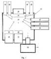
- FIG. 1is a schematic representation of a sputtering system used in the fabrication of certain zinc oxide crystal growth substrates.
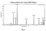
- FIG. 2is graph of the X-ray diffraction pattern generated by sputtered arsenic doped polycrystalline zinc oxide.
- FIG. 3is a graph of the X-ray diffraction pattern generated by a zinc oxide thin film within the scope of the present invention showing single crystal (002) plane.
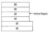
- FIG. 4is a schematic diagram of a zinc semiconductor heterostructure device containing an active region.
- FIG. 5is a schematic diagram of a zinc oxide semiconductor device of FIG. 3 without an active region.
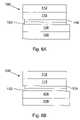
- FIG. 6Ais a schematic diagram of a conventional GaN solid state device fabricated on a sapphire or SiC substrate.
- FIG. 6Bis a schematic diagram of a ZnO solid state device fabricated on an alternative self-supporting substrate within the scope of the present invention.
- FIGS. 7A–7Bare schematic representations of zinc oxide semiconductor devices fabricated with multiple quantum wells.
- FIGS. 8A–8Bare schematic representations of zinc oxide semiconductor devices fabricated with a single quantum well.
- the present inventionis drawn to a zinc oxide crystal growth substrate.
- the zinc oxide crystal growth substrateincludes a thin layer of single crystal zinc oxide deposited on an self supporting substrate surface by a chemical deposition process.
- the self supporting substratemay be amorphous, polycrystalline, or crystalline.
- single crystal zinc oxideincludes zinc oxide with a single predominant reflection on an X-ray diffraction pattern.
- Polycrystalline zinc oxidewill possess multiple reflection peaks on an X-ray diffraction pattern. Persons skilled in the art will appreciate that a perfect single crystal, defect free, does not exist. There will always be some minor crystal defects present.
- a single predominant reflection peakwill possess at least 95% of the integrated area of the X-ray diffraction pattern, and more preferably greater than 99%.
- the single crystal zinc oxidemay be oriented in the (002) plane.
- the zinc oxidemay be oriented in other crystal planes depending on the crystal orientation of the self supporting substrate. For example, if (111) silicon or (111) sapphire is used as the self-supporting substrate, then (111) ZnO may be prepared.
- the thin layer of zinc oxidehas a crystal lattice which permits the crystal growth of a crystal compatible with zinc oxide.
- the compatible crystalpreferably has a lattice parameter within about 5% of a corresponding lattice parameter of the zinc oxide.
- Table 1several compatible crystals are shown in Table 1, some of which have lattice parameter mismatches that exceed 5%.
- the self supporting substratemay be a low-cost substrate, including but not limited to, amorphous fused silica (SiO 2 ), polycrystalline alumina, or crystalline silicon wafer.
- the amorphous substratemay also include an amorphous SiO 2 coating on silicon wafer which may be a native oxide layer or a grown oxide layer.
- the self supporting substratemay include commonly used crystalline substrate materials, including but not limited to, silicon carbide and sapphire.
- fused silicamay be used successfully as a self supporting substrate for single crystal zinc oxide.
- Amorphous fused silicapossesses bond angles that can change readily and sustain strain.
- some common crystalline substrate materialscannot support the strain created by different crystals grown thereon.
- the compatible crystalmay include, but is not limited to GaN, AlN, SiC, and ZnO.
- GaN, AlN, SiC, and ZnOmay be useful for the fabrication semiconductor electronic devices, discussed above.
- AlN and SiCmay also be useful used as a thermal management substrate because of their high thermal conductivity.
- AlN and pure, grown SiChave high resistivity, AlN and SiC may replace BeO (beryllia) in microelectronics thermal management applications.
- the zinc oxide substratedoes not need to be n-type or p-type doped. It is important that the substrate be a single crystal with a lattice that closely matches the crystal grown thereon.
- Single crystal zinc oxideexhibits intrinsic n-type conduction due to the presence of excess donors.
- the electrical properties of the zinc oxidemay be modified during deposition by incorporating either a p-type dopant or an n-type dopant.
- Zinc oxide based semiconductor devices containing a p-n junctionmay be readily fabricated utilizing a zinc oxide substrate within the scope of the present invention.
- the n-type zinc oxidemay contain an n-type dopant selected from known dopant materials. Typical n-type dopants include, but are not limited to, ions of Al, Ga, B, H, Yb and other rare earth elements, Y, Sc, and mixtures thereof.
- the p-type zinc oxidemay contain a p-type dopant selected from known p-type dopant materials.
- Typical p-type dopantsinclude, but are not limited to, nitrogen, phosphorus, arsenic, antimony, bismuth, copper, chalcogenides of the foregoing, and mixtures thereof.
- the chemical deposition processis preferably a commercially viable process including, but not limited to RF sputtering, CVD (chemical vapor deposition), MOCVD (metal organic chemical vapor deposition), spin coating, electrophoresis, and hydrothermal growth processes.
- Such processesmay be used to deposit a thin layer of zinc oxide having a thickness less than about 5 ⁇ m. Thicker layers may be built up by repeating the deposition process.
- the chemical deposition processincluded RF sputtering using an RF sputtering system having a zinc metal target, a substrate surface, and a plasma comprising oxygen and an inert sputtering gas.
- the RF sputtering systemoperated at conditions which produced the thin layer of single crystal zinc oxide on the substrate surface.
- a substrateis placed in a low-pressure chamber.
- the magnetron sputtering headis driven by an RF power source which generates a plasma and ionization of the gas or gases (e.g., argon and selected dopants).
- a high-frequency generatoris used generating electromagnetic power in the MHz-Region (typically about 13.56 MHz).
- Argon ionsbombard the target releasing ions from the target which are liberated and accelerated towards the substrate. Additional atoms in the plasma may also be deposited onto the substrate.
- the systemmay operate at a power in the range from about 20 to about 120 watts. Persons skilled in the art will appreciate that the power may be varied to control deposition time and film thickness, as well as the quality of the resulting film.
- the inert sputtering gasis present in the sputtering atmosphere at a pressure in the range from about 4 to 20 mtorr.
- the inert sputtering gasis preferably selected from argon, krypton, xenon, neon, and helium.
- Argonis a presently preferred inert sputtering gas.
- Small amounts of oxygenmay be included in the sputtering gas, usually at a pressure in the range from about 1 to 4 mtorr.
- beneficial resultshave been obtained when the thin film is annealed at a temperature in the range from about 300 to about 430° C. for a time period in the range from about 1 to about 15 minutes.
- a combination of sputtering and thermal evaporationmay also be used to deposit the zinc oxide more quickly.
- Spin coatingis another useful process for depositing the thin film of zinc oxide.
- An organic molecule containing zincsuch as zinc 2–4 pentanedionate is used as the zinc source.
- a solution of this compound dissolved in a suitable solvent, such as butanol,is spun onto the substrate, such as fused silica. After a layer is spun on the substrate, it is heated to about 600° C. for about 10 minutes for pyrolysis of the organics. This procedure is repeated 5 or 6 times to get the desired film thickness.
- the substrateis annealed at about 700° C. for 1 to 5 hours in a nitrogen atmosphere. The required oxygen can come from the atmosphere or can come from being part of the organic precursors.
- a single crystal zinc oxide crystal growth substratemay be prepared by metal organic chemical vapor deposition (MOCVD).
- MOCVDis a modified chemical vapor deposition process that works similar to the spin coating processes described above.
- the organic compoundsmay or may not be dissolved in a solvent. The difference being that the organic compounds are sprayed onto a spinning substrate, and the solvent is allowed to evaporate during deposition. The process occurs in a partial vacuum.
- the substrateoften spins at a rate of about 50–100 rpm, and as high as 600 rpm.
- the organic compoundsare forced through heated nozzles. The nozzles heat the liquid to the vapor point, and the vaporized compounds mix in a mixing chamber.
- Other compoundsmay be optionally added in the mixing chamber, such as nitrogen, ammonia, or dopants.
- the substrate surfaceis heated to a temperature of about 500 to 700° C. to cause pyrolysis.
- the organic compoundsmust be pyrolyzed in order to leave behind the desired metal oxide composition.
- the organic constituentsare engineered to be chemically bound into the same organic compound and sometimes each constituent is sprayed onto the substrate through separate nozzles.
- FIG. 1illustrates a schematic representation of a sputtering system 10 used in some of the following examples.
- a substrate 12is placed in a low-pressure chamber 14 .
- the magnetron sputtering head 16is driven by an RF power source (not shown) which generates a plasma and ionization of the sputtering gas or gases between the electrodes.
- the sputtering gastypically includes an inert sputtering gas, which may include, but is not limited to, argon, krypton, xenon, neon, and helium.
- the sputtering gasmay optionally include one or more selected dopants.
- a plurality of gas sources 18 , 20 , 22 , and 24may provide N 2 , H 2 , Ar, O 2 , or other desired gases.
- a high-frequency generatoris used generating electromagnetic power in the MHz-Region.
- Argon ionsbombard the target 26 , releasing ions from the target which are accelerated towards the substrate. Additional atoms in the plasma may also be deposited onto the substrate, such as dopant atoms.
- the substrate 12is secured in place by a heated substrate fixture 28 .
- the temperature of the heated substrate fixture 28was measured and reported as the substrate temperature.
- the sputtering chamber 14is constantly evacuated with a vacuum pump system 30 .
- the sputtering atmosphereincludes an inert sputtering gas mentioned above, and may optionally include other gases which are provided by the respective gas source 18 , 20 , 22 , and 24 .
- volatile materials 32such as arsenic for example, are evaporated in a heated basket, illustrated as the heated evaporator 34 .
- the systemincludes online pressure measurement 36 . It also includes thickness measurement capability 38 .
- the systemoptionally includes an online mass spectrometer 40 which may measure the gas content and accurately determine the partial pressure of the sputtering atmosphere.
- the distance between the sputtering target and the deposition substratewas about 1.5 inches.
- Radio Frequencywas 13.56 MHz. It will be appreciated by those skilled in the art that much lower and much higher frequencies may be used in RF sputtering systems. However, for practical considerations and FCC regulations, the radio frequency used was 13.56 MHz.
- the atmospherewas maintained by using a continuous vacuum, and pressures were controlled by addition of indicated gases. Some residual atmospheric oxygen or moisture adsorbs on the metal surfaces within the sputtering chamber. Therefore, oxygen out gases during the sputtering process at the operating temperature and pressure.
- the sputtering timewas typically about 10 minutes, but some samples were sputtered for longer time periods, such as an hour, and some samples were sputtered for shorter periods, such as one minute.
- the sputtering timewas selected to produce a film thickness of about one micron. It will be appreciated that several factors affect the film thickness, including, but not limited to, sputtering time, power, temperature, concentration of dopants, and evaporation of constituents of the sputtered thin film.
- One inch RF magnetron sputtering headwas used with water cooling.
- a thin film of undoped zinc oxidewas deposited onto a self supporting substrate by RF sputtering. Both fused silica and silicon wafers were used as the self supporting substrate.
- the sputtering target compositionwas ZnO.
- the substrate temperaturewas between 350 and 550° C.
- the preferred temperaturewas about 400° C.
- the RF powerwas between 20 and 120 watts.
- the preferred powerwas about 60 watts.
- the sputtering atmosphereincluded argon at a gas pressure of about 4 to 20 mtorr and O 2 at a gas pressure of about 1 to 4 mtorr.
- the preferred sputtering atmosphere pressureswere about 9 mtorr argon and about 1 mtorr O 2 .
- a thin film of p-type zinc oxidewas deposited onto a self supporting substrate by RF sputtering. Both fused silica and silicon wafers were used as the self supporting substrate.
- the sputtering target compositionwas ZnO (0.99–0.95 moles)+As (0.01–0.05 moles).
- the preferred target compositionwas ZnO (0.98 moles)+As (0.02 moles).
- the substrate temperaturewas between 350 and 550° C.
- the preferred temperaturewas about 400° C.
- the RF powerwas between 20 and 120 watts.
- the preferred powerwas about 60 watts.
- the sputtering atmosphereincluded argon at a gas pressure of about 4 to 20 mtorr and O 2 at a gas pressure of about 1 to 4 mtorr.
- the preferred sputtering atmosphere pressureswere about 9 mtorr argon and about 1 mtorr O 2 .
- the resulting transparent p-type zinc oxide layerhad a resistance of about 10,000 ohms/square. After annealing at 440° C. in air, the resistance dropped to about 1,000 ohms/square.
- the transparent p-type zinc oxide layerhad a resistance ranging from 200,000 ohms/square to 10,000,000 ohms/square. This composition was not subsequently annealed.
- a thin film of p-type zinc oxidewas deposited onto a self supporting substrate by RF sputtering. Both fused silica and silicon wafers were used as the self supporting substrate.
- the sputtering target compositionwas ZnO (0.99–0.95 moles)+As (0.01–0.05 moles).
- the preferred target compositionwas ZnO (0.98 moles)+As (0.02 moles).
- the substrate temperaturewas between 350 and 550° C.
- the preferred temperaturewas about 400° C.
- the RF powerwas between 20 and 120 watts.
- the preferred powerwas about 60 watts.
- the sputtering atmosphereincluded argon at a gas pressure of about 4 to 20 mtorr and H 2 at a gas pressure of about 1 to 4 mtorr.
- the preferred sputtering atmosphere pressureswere about 9 mtorr argon and about 1 mtorr H 2 .
- the resulting transparent p-type zinc oxide layerhad a resistance of about 500 ohms/square. Without being bound by theory, it is believed that the hydrogen gas may moderate the concentration of oxygen in the sputtering atmosphere.
- a thin film of p-type zinc oxidewas deposited onto a self supporting substrate by RF sputtering. Both fused silica and silicon wafers were used as the self supporting substrate.
- a First Composition Layercomprising zinc and arsenic was deposited onto the self supporting substrate.
- the First Composition Layerwas deposited by thermal evaporation of zinc arsenide (Zn 3 As 2 or ZnAs 2 ) for a period of about 2–60 seconds, with a preferred period of about 14 seconds.
- the substrate temperaturewas about 360° C.
- Subsequent analysis of the First Composition Layerindicated that it contained zinc and arsenic in approximately equal atomic amounts. This suggests that the stoichiometry of the zinc arsenide had changed during thermal evaporation.
- Thermal evaporationis a well known technique for depositing thin films, particularly metal and metal alloys.
- the following sequential basic stepstake place: (i) a vapor is generated by boiling or subliming a source material, (ii) the vapor is transported from the source to the substrate, and (iii) the vapor is condensed to a solid film on the substrate surface.
- a substrateis placed in a low-pressure chamber.
- a tungsten crucibleis disposed below the substrate.
- the desired source material or mixture of source materialsis placed in the crucible and heated to a temperature sufficiently high to evaporate the source material.
- the source material vaporcondenses on the substrate, which may or may not be heated. Heating the substrate may enhance the bond between the deposited source material film and the substrate.
- the evaporative deposition processmay be completed in less than a minute, and usually a few seconds.
- the First Composition Layerwas deposited by RF sputtering. In yet another example, the First Composition Layer was deposited by the combination of thermal evaporation and RF sputtering. It will be appreciated that the First Composition Layer may be deposited using other known, conventional, or novel deposition techniques, including, but not limited to, RF sputtering and evaporative deposition techniques described above, as well as chemical vapor deposition (CVD), metal organic chemical vapor deposition (MOCVD), other evaporation and sputtering techniques, and combinations of these and other thin film deposition technologies.
- CVDchemical vapor deposition
- MOCVDmetal organic chemical vapor deposition
- Preparing a thin film by evaporation aloneis a very quick process that is completed in a matter of seconds, but it is difficult to properly control the resulting thin film.
- sputtering aloneis a slow process that requires many minutes to complete.
- the combination of sputtering and thermal evaporationincludes heat to facilitate evaporation of the source material and a RF field to induce sputtering.
- the RF fieldcan be used to heat the source material disposed close to the RF magnetron head sufficiently to evaporate the source material for deposition by thermal evaporation. In this case, a small amount of sputtering will also occur.
- the resulting thin filmis of good quality and quickly prepared.
- the combination of sputtering and evaporationwas used to deposit Zn 3 As 2 onto a fused silica substrate at 350° C. for about 50 seconds.
- a Second Composition Layer comprising zinc oxidewas deposited onto the First Composition Layer by RF sputtering.
- the sputtering target compositionwas ZnO.
- the substrate temperaturewas between 400 and 550° C.
- the preferred temperaturewas about 450° C.
- the RF powerwas between 20 and 120 watts.
- the preferred powerwas about 100 watts.
- the sputtering timewas between 10 and 40 minutes, and preferably about 20 minutes.
- the sputtering atmosphereincluded argon at a gas pressure of about 4 to 20 mtorr.
- the preferred sputtering atmosphere pressurewas about 10 mtorr argon.
- a region of the arsenic doped p-type zinc oxide that was sputtered directly onto a fused silica substratewas analyzed by X-ray diffraction.
- a graph of the X-ray diffraction patternis shown in FIG. 3 illustrating a single dominant peak representing the (002) plane. This indicates that single crystal p-type zinc oxide was deposited directly onto the amorphous fused silica substrate.
- an X-ray diffraction pattern of polycrystalline zinc oxideis shown in FIG. 2 .
- a thin film of p-type zinc oxidewas deposited onto a self supporting substrate by RF sputtering. Both fused silica and silicon wafers were used as the self supporting substrate.
- the sputtering target compositionwas Zn (0.99–0.95 moles)+As 2 O 3 (0.01–0.05 moles).
- the preferred target compositionwas about Zn (0.99 moles)+As 2 O 3 (0.01 moles).
- the substrate temperaturewas between 350 and 550° C.
- the preferred temperaturewas about 400° C.
- the RF powerwas between 15 and 40 watts.
- the preferred powerwas about 30 Watts.
- a lower powerwas used in this example to keep the powdered zinc metal in the target from being quickly vaporized and dispersed during the sputtering processing.
- the sputtering atmosphereincluded argon at a gas pressure of about 4 to 20 mtorr and O 2 at a gas pressure of about 1 to 4 mtorr.
- the preferred sputtering atmosphere pressureswere about 10 mtorr argon and about 1 mtorr O 2 .
- the resulting transparent p-type zinc oxide layerhad a resistance of about 100,000 ohms/square.
- a thin film of p-type zinc oxidewas deposited onto a self supporting substrate by RF sputtering. Both fused silica and silicon wafers were used as the self supporting substrate.
- the sputtering target compositionwas ZnO (0.99–0.95 moles)+As 2 O 3 (0.01–0.05 moles).
- the preferred target compositionwas ZnO (0.99 moles)+As 2 O 3 (0.01 moles).
- the substrate temperaturewas between 350 and 550° C.
- the preferred temperaturewas about 400° C.
- the RF powerwas between 20 and 120 watts.
- the preferred powerwas about 60 watts.
- the sputtering atmosphereincluded argon at a gas pressure of about 4 to 20 mtorr.
- the preferred sputtering atmosphere pressurewas about 10 mtorr argon.
- the resulting transparent p-type zinc oxide layerhad a resistance of about 100,000 ohms/square.
- a thin film of p-type zinc oxidewas deposited onto a self supporting substrate by RF sputtering. Both fused silica and silicon wafers were used as the self supporting substrate.
- the sputtering target compositionwas Zn (0.99–0.95 moles)+Sb (0.01–0.05 moles).
- the preferred target compositionwas Zn (0.99 moles)+Sb (0.01 moles).
- the substrate temperaturewas between 350 and 550° C.
- the preferred temperaturewas about 400° C.
- the RF powerwas between 20 and 120 watts.
- the preferred powerwas about 60 watts.
- the sputtering atmosphereincluded argon at a gas pressure of about 4 to 20 mtorr.
- the preferred sputtering atmosphere pressurewas about 10 mtorr argon.
- the resulting transparent p-type zinc oxide layerhad a resistance of about 600,000 ohms/square. Without being bound by theory, it is believed that the oxygen needed to form the zinc oxide crystal lattice was obtained from residual oxygen in the sputtering system atmosphere.
- the target compositionis not limited to metallic zinc and antimony.
- the targetmay comprise zinc oxide and antimony metal, zinc metal and antimony oxide, and zinc oxide and antimony oxide.
- the sputtering atmospheremay include hydrogen gas at a gas pressure of about 0.1 to 4 mtorr in addition to the inert sputtering gas.
- Antimony-doped zinc oxidemay also be prepared in a manner similar to Example 4 in which a First Composition Layer containing zinc and antimony is deposited. Antimony-doped zinc oxide has been prepared in a manner similar to Example 4 in which the First Composition Layer contains just antimony.
- a thin film of p-type zinc oxidewas deposited onto a self supporting substrate by RF sputtering. Both fused silica and silicon wafers were used as the self supporting substrate.
- a First Composition Layer comprising copperwas deposited onto the self supporting substrate by RF sputtering for a period of from 5 to 40 minutes, with a preferred period of about 10 minutes at room temperature.
- a Second Composition Layer comprising zinc oxidewas deposited onto the First Composition Layer by RF sputtering.
- the sputtering target compositionwas ZnO.
- the substrate temperaturewas between 400 and 550° C.
- the preferred temperaturewas about 450° C.
- the RF powerwas between 20 and 120 watts.
- the preferred powerwas about 100 watts.
- the sputtering timewas between 10 and 40 minutes, and preferably about 20 minutes.
- the sputtering atmosphereincluded argon at a gas pressure of about 4 to 20 mtorr.
- the preferred sputtering atmosphere pressurewas about 10 mtorr argon.
- coppermay counteract the natural n-type property of ZnO resulting in a neutral or p-type semiconductor with low resistance. Without being bound by theory, it is believed that a quantity of copper may be evaporated during the sputtering step and become part of the sputtering plasma such that ZnO doped with copper was deposited onto substrate.
- a thin film of p-type zinc oxidewas deposited- onto a self supporting substrate by RF sputtering. Both fused silica and silicon wafers were used as the self supporting substrate.
- a First Composition Layer comprising zinc and arsenicwas deposited onto the self supporting substrate.
- the First Composition Layerincluded Zn 3 As 2 , ZnAs 2 , or a mixture thereof.
- the zinc/arsenic layerwas deposited by thermal evaporation for a period of about 2–60 seconds, with a preferred period of about 14 seconds. The temperature was about 360° C.
- the First Composition Layermay also be deposited by RF sputtering.
- a Second Composition Layer comprising zinc oxidewas deposited onto the First Composition Layer by RF sputtering.
- the sputtering target compositionwas ZnO.
- the substrate temperaturewas between 400 and 550° C.
- the preferred temperaturewas about 450° C.
- the RF powerwas between 20 and 120 watts.
- the preferred powerwas about 100 watts.
- the sputtering timewas between 10 and 40 minutes, and preferably about 20 minutes.
- the sputtering atmosphereincluded argon at a gas pressure of about 4 to 20 mtorr and hydrogen at a gas pressure of about 0.1 to 4 mtorr.
- the preferred sputtering atmosphere pressurewas about 10 mtorr argon and about 1 mtorr hydrogen.
- the resulting p-type zinc oxide layerhad a resistance of about 10 to 200 ohms/square.
- a thin film of p-type zinc oxidewas deposited onto a self supporting substrate by RF sputtering.
- Fused silicawas used as the self supporting substrate.
- the sputtering target compositionwas ZnO.
- the substrate temperaturewas between 350 and 550° C.
- the preferred temperaturewas about 400° C.
- the RF powerwas between 20 and 120 watts.
- the preferred powerwas about 60 watts.
- the sputtering atmosphereincluded argon at a gas pressure of about 4 to 20 mtorr.
- a basket containing arsenicwas heated to a controlled temperature sufficient to evaporate the arsenic. The basket was positioned such that the arsenic was evaporated directly onto the fused silica at the same time the zinc oxide was sputtered onto the fused silica.
- the resulting transparent p-type zinc oxide layerdisplayed visible diffraction rings, but was very clear and transparent. It will be appreciated that this process may be adapted for use with other p-type dopants besides arsenic.
- As 4Based upon arsenic vapor pressure data, As 4 has a higher vapor pressure at a given temperature when compared to As 3 , As 2 , and As. Therefore, it is presently believed that As 4 is the dominant volatile arsenic species at typical operating conditions. Without being bound by theory, it is believed As 4 must be broken into individual arsenic atoms to be incorporated into the zinc oxide. An apparent threshold RF power of about 60 watts has been observed for the given experimental sputtering system used herein. It will be appreciated that this threshold RF power may vary depending upon the sputtering system used. Likewise, it will be appreciated that other means besides a RF field may be used to break the As 4 molecular bonds.
- a stable, p-type zinc oxide semiconductor materialwas prepared.
- Zinc metal, doped with 2 mole % arsenicwas deposited onto a fused silica substrate by thermal evaporation in an oxygen-rich atmosphere containing 20 mtorr argon and 10 mtorr oxygen at a temperature of about 430° C.
- the zinc and/or arsenicwas partially oxidized.
- the resulting As-doped ZnO thin filmexhibited p-type characteristics. It had a Seebeck voltage of about positive 6 mV D.C. Increasing the oxygen pressure may result in a more complete formation of ZnO. While no further heating or annealing was performed in this example, additional heating or annealing may be desirable to control the level of zinc oxidation and/or optimize the electronic properties of the p-type semiconductor material.
- a stable, p-type zinc oxide semiconductor materialmay be prepared by spin coating using arsenic as the dopant.
- Fused silicais used as the self supporting substrate.
- Zinc 2–4 pentanedionateis used as the zinc source and arsenic III ethoxide is used as the arsenic source.
- These compoundsare dissolved in butanol which serves as a common solvent. This solution is spun onto a fused silica slide.
- a layeris spun on the substrate, it is heated to about 600° C. for about 10 minutes for pyrolysis of the organics. This procedure is repeated 5 or 6 times to get the desired film thickness.
- the substrateis annealed at about 700° C. for 1 to 5 hours in a nitrogen atmosphere. Control of the partial pressures of all inorganic components is desirable for the desired doped zinc oxide composition, otherwise evaporation or one or more ingredients or formation of undesired compounds may occur.
- the oxygencan come from the atmosphere or can come from being part of the organic precursors.
- a stable, p-type zinc oxide semiconductor materialmay be prepared by spin coating in accordance with the method of Example 12, except that antimony is used as the dopant instead of arsenic.
- Antimony chloride (SbCl 3 )is used as the antimony source.
- a stable, p-type zinc oxide semiconductor materialmay be prepared by metal organic chemical vapor deposition (MOCVD) using arsenic, antimony, or other p-type dopant.
- MOCVDmetal organic chemical vapor deposition
- the typical MOCVD processis described above.
- a zinc oxide p/n junctionwas fabricated.
- a thin film of p-type zinc oxidewas deposited onto a self supporting silicon wafer substrate by RF sputtering in accordance with Example 4.
- a thin film of zinc arsenidewas first deposited onto the silicon wafer and the p-type zinc oxide was sputtered on top of the zinc arsenide.
- a thin film of n-type zinc oxidewas sputtered on top of the p-type zinc oxide at about 300° C.
- the sputtering targetincluded ZnO (99.925 mole %) and Ga 2 O 3 (0.075 mole %) that had been mixed, sintered, and annealed at about 1100° C.
- the sputtering stepoccurred at a temperature of about 350° C.
- the sputtering atmosphereincluded argon at a gas pressure of about 4 to 20 mtorr. About 10% hydrogen gas may alternatively be included in the sputtering atmosphere to produce n-type zinc oxide. Electrodes were attached to the p/n junction. Current vs. voltage was measured to show rectification of the p/n junction. A luminescent emission at room temperature was briefly observed before the p/n junction failed. Failure occurred because the electrical resistance dropped too quickly allowing excessive current to overpower the p/n junction.
- Semiconductor heterostructuresmay be fabricated based upon p/n junction described above. These devices may be prepared by depositing multiple layers of p-type and n-type semiconductors. Such heterostructures may be fabricated using matching or compatible semiconductor crystals. Examples of two possible semiconductor heterostructure devices are illustrated in FIGS. 4 and 5 . It will be appreciated that the illustrated devices are given by way of example and not limitation. Persons skilled in the art will recognize that numerous variations of these devices are possible.
- the device shown in FIG. 4includes a self supporting substrate 50 .
- the substratemay be a known crystalline substrate or it may be a low cost substrate including, but not limited to, silicon wafers, polycrystalline alumina, and amorphous self supporting substrate surfaces like fused silica.
- the n-type zinc oxide layer 52may be about 0.4 ⁇ m thick.
- the devicemay include additional n-type zinc oxide layers 54 , 56 , comprising magnesium and cadmium alloys.
- layer 54may have a composition of Mg .15 Zn .85 O doped with gallium, and it may have a thickness of about 0.15 ⁇ m.
- Layer 56may have a composition of Cd .06 Zn .94 O doped with gallium, and it may have a thickness of about 0.05 ⁇ m.
- the thin cadmium zinc oxide alloy layer 56is the active region wherein light generation occurs.
- Deposited on top of the active region layer 56are one or more p-type zinc layers 58 , 60 .
- Layer 58may have a composition of Mg .15 Zn .85 O doped with arsenic, and it may have a thickness of about 0.15 ⁇ m.
- Layer 60may be p-type zinc oxide doped with a p-type dopant, such as arsenic.
- composition of the n-type and p-type zinc oxide layersmay vary.
- concentration of magnesium and cadmium in the zinc oxide alloysmay vary.
- FIG. 5illustrates a device substantially identical to the device of FIG. 4 , except that there is no separate active region.
- Single or multiple quantum well (MQW) heterostructuresmay be fabricated to render the p/n junction more efficient.
- a single quantum wellis made of two alternating semiconductor materials. One layer is a barrier layer defined by a higher band gap than the second layer. The second layer's band gap defines the bottom of the quantum well.
- MgOmay be alloyed with ZnO to form the barrier layer, and the undoped ZnO will define the bottom of the well. This produces a more efficient device and raises the band edge.
- CdOmay be alloyed with ZnO to define the bottom layer of the quantum well, and the undoped ZnO defines the barrier layer. This produces a more efficient device and lowers the band edge.
- An additional advantage of a quantum wellis that the layers can be mechanically strained to raise or lower the band edge. Mechanical strain may exist if the two layers have slightly different crystal lattice constants. For most zinc oxide materials the band edge is around 390 nm, but some of the zinc oxide semiconductor materials fabricated in accordance with the present invention had a band edge of about 370 nm.
- the number of quantum wellsmay vary. Good results may be obtained with just one quantum well. Typically the number of quantum wells may range from about 1 to 10, and more preferably from about 3 to 7 quantum wells.
- the total thickness of the quantum well alternating layersmust in the vicinity of, or less than, the electron de Broglie wavelength (100 ⁇ ).
- These heterostructuresmay be fabricated through a chemical deposition process, including but not limited to those described above, such as sputtering, CVD, MOCVD, etc.
- FIG. 6Ais a schematic representation of a typical state of the art GaN-based semiconductor device 80 containing MQWs 82 . It will be appreciated that GaN devices are complicated to manufacture because of the expensive sapphire or SiC substrate 84 and multiple layers 86 , 88 required to match the crystal lattice of GaN and the substrate.
- FIG. 6Bis a schematic representation of a zinc oxide based semiconductor device 90 containing MQWs 92 . Because single crystal zinc oxide 94 may be deposited directly on a low-cost substrate 96 , such as fused silica or a silicon wafer, the zinc oxide based semiconductor device fabricated within the scope of the present invention represents a substantial improvement over conventional GaN-based semiconductor devices.
- FIG. 7Ais a schematic representation of one possible zinc oxide based semiconductor device 100 fabricated with MQWs. Three quantum wells are shown containing alternating layers of undoped ZnO 102 (20 ⁇ –100 ⁇ ) and Cd .2 Zn .8 O 104 (10 ⁇ –25 ⁇ ).
- the cadmium contentmay be varied.
- the amount of cadmium in the cadmium zinc oxide alloy 104may vary depending on the desired shifting of the band gap.
- the cadmium contentpreferably ranges from about 1 to 20 mole %, and more typically about 10 mole %.
- the semiconductor device 100includes a layer of n-type zinc oxide 106 , approximately 2 ⁇ m thick, doped with an n-type dopant, such as Ga or Al, deposited on a self supporting substrate 108 .
- a layer of p-type zinc oxide 110approximately 2 ⁇ m thick, doped with a p-type dopant, such as arsenic, may be deposited on top of the MQWs, layers 102 , 104 .
- a layer of p-type zinc oxide 112approximately 5 ⁇ m thick, doped with a p-type dopant, such as arsenic, may be deposited on top of layer 110 .
- FIG. 7Bis a schematic representation of a zinc oxide based semiconductor device 120 similar to that of FIG. 7A except that the quantum wells include a magnesium zinc oxide alloy instead of a cadmium zinc oxide alloy.
- the alternating layers of magnesium zinc oxide alloy 124may have the formula Mg .1 Zn .9 O (10 ⁇ –25 ⁇ ).
- the magnesium contentmay be varied.
- the amount of magnesium the magnesium zinc oxide alloy 124may vary depending on the desired shifting of the band gap.
- the magnesium contentpreferably ranges from about 1 to 20 mole %, and more typically about 10 mole %.
- FIG. 8Ais a schematic representation of one possible zinc oxide based semiconductor device fabricated with a single quantum well having a composition substantially the same as the device shown in FIG. 7A .
- the number of quantum wellscan vary, just as the composition of the quantum well layers and the p-type and n-type semiconductor material used in the device.
- FIG. 8Bis a schematic representation of a zinc oxide based semiconductor device similar to that of FIG. 8A except that the quantum well includes a magnesium zinc oxide alloy instead of a cadmium zinc oxide alloy.
- the present inventionprovides zinc oxide crystal growth substrates useful for a variety of different applications.
- the zinc oxide substratesare commercially viable.
Landscapes
- Engineering & Computer Science (AREA)
- Chemical & Material Sciences (AREA)
- Manufacturing & Machinery (AREA)
- Physics & Mathematics (AREA)
- Computer Hardware Design (AREA)
- Microelectronics & Electronic Packaging (AREA)
- Power Engineering (AREA)
- Condensed Matter Physics & Semiconductors (AREA)
- General Physics & Mathematics (AREA)
- Materials Engineering (AREA)
- Crystallography & Structural Chemistry (AREA)
- Metallurgy (AREA)
- Organic Chemistry (AREA)
- Inorganic Chemistry (AREA)
- Chemical Kinetics & Catalysis (AREA)
- General Chemical & Material Sciences (AREA)
- Crystals, And After-Treatments Of Crystals (AREA)
- Physical Deposition Of Substances That Are Components Of Semiconductor Devices (AREA)
Abstract
Description
| TABLE 1 | |||
| Thermal | |||
| Lattice | Expansion | ||
| Lattice | Parameters | Coefficient | |
| Crystal | Type | [nm] | [106/K] |
| GaN | hexagonal (wurtzite) | a = 0.3189 | 5.59 |
| c = 0.5185 | 3.17 | ||
| Alpha-Al2O3 | hexagonal (wurtzite) | a = 0.4758 | 7.5 |
| c = 1.2991 | 8.5 | ||
| 6H—SiC | hexagonal (sphalerite) | a = 0.3081 | 4.2 |
| c = 1.511 | 4.68 | ||
| NdGaO3 | Orthorhombic | a = 0.5422 | 11.9 |
| b = 0.5499 | 6.6 | ||
| c = 0.7708 | 5.8 | ||
| YSZ | Cubic (fluorite) | a = 0.515 | 11.4 |
| Si | Cubic silicon | a = 0.3431 | 2.44 |
| ZnO | hexagonal (wurtzite) | a = 0.3252 | 2.9 |
| c = 0.5213 | 4.75 | ||
Claims (33)
Priority Applications (2)
| Application Number | Priority Date | Filing Date | Title |
|---|---|---|---|
| US10/849,332US7172813B2 (en) | 2003-05-20 | 2004-05-19 | Zinc oxide crystal growth substrate |
| PCT/US2004/015881WO2004104274A2 (en) | 2003-05-20 | 2004-05-20 | Zinc oxide crystal growth substrate |
Applications Claiming Priority (4)
| Application Number | Priority Date | Filing Date | Title |
|---|---|---|---|
| US47191603P | 2003-05-20 | 2003-05-20 | |
| US48867703P | 2003-07-18 | 2003-07-18 | |
| US56042704P | 2004-04-08 | 2004-04-08 | |
| US10/849,332US7172813B2 (en) | 2003-05-20 | 2004-05-19 | Zinc oxide crystal growth substrate |
Publications (2)
| Publication Number | Publication Date |
|---|---|
| US20040234823A1 US20040234823A1 (en) | 2004-11-25 |
| US7172813B2true US7172813B2 (en) | 2007-02-06 |
Family
ID=33459150
Family Applications (1)
| Application Number | Title | Priority Date | Filing Date |
|---|---|---|---|
| US10/849,332Expired - Fee RelatedUS7172813B2 (en) | 2003-05-20 | 2004-05-19 | Zinc oxide crystal growth substrate |
Country Status (2)
| Country | Link |
|---|---|
| US (1) | US7172813B2 (en) |
| WO (1) | WO2004104274A2 (en) |
Cited By (13)
| Publication number | Priority date | Publication date | Assignee | Title |
|---|---|---|---|---|
| US20050285119A1 (en)* | 2004-06-17 | 2005-12-29 | Burgener Robert H Ii | Dynamic p-n junction growth |
| US20080308805A1 (en)* | 2005-09-29 | 2008-12-18 | Semiconductor Energy Laboratory Co., Ltd. | Semiconductor Device and Manufacturing Method Thereof |
| US20100102307A1 (en)* | 2006-04-25 | 2010-04-29 | National University Of Singapore | Method of zinc oxide film grown on the epitaxial lateral overgrowth gallium nitride template |
| US20110085944A1 (en)* | 2006-08-15 | 2011-04-14 | Battelle Energy Alliance, Llc | Systems including catalysts in porous zeolite materials within a reactor for use in synthesizing hydrocarbons |
| WO2011133999A1 (en)* | 2010-04-30 | 2011-11-03 | Commonwealth Scientific And Industrial Research Organisation | Crystallisation facilitators for the synthesis of metal organic frameworks |
| US8638111B2 (en) | 2010-06-17 | 2014-01-28 | Caterpillar Inc. | Zinc oxide sulfur sensor measurement system |
| US8653839B2 (en) | 2009-07-17 | 2014-02-18 | Caterpillar Inc. | Zinc oxide sulfur sensors and method of using said sensors |
| US8829556B2 (en) | 2011-09-01 | 2014-09-09 | General Electric Company | Thermal management in large area flexible OLED assembly |
| US9305778B2 (en) | 2012-11-16 | 2016-04-05 | Samsung Electronics Co., Ltd. | Controlled manufacturing method of metal oxide semiconductor and metal oxide semiconductor structure having controlled growth crystallographic plane |
| US9806125B2 (en) | 2015-07-28 | 2017-10-31 | Carrier Corporation | Compositionally graded photodetectors |
| US9865766B2 (en) | 2015-07-28 | 2018-01-09 | Carrier Corporation | Ultraviolet photodetectors and methods of making ultraviolet photodetectors |
| US9928727B2 (en) | 2015-07-28 | 2018-03-27 | Carrier Corporation | Flame detectors |
| US10126165B2 (en) | 2015-07-28 | 2018-11-13 | Carrier Corporation | Radiation sensors |
Families Citing this family (11)
| Publication number | Priority date | Publication date | Assignee | Title |
|---|---|---|---|---|
| US20070126021A1 (en)* | 2005-12-06 | 2007-06-07 | Yungryel Ryu | Metal oxide semiconductor film structures and methods |
| US7977169B2 (en)* | 2006-02-15 | 2011-07-12 | Kochi Industrial Promotion Center | Semiconductor device including active layer made of zinc oxide with controlled orientations and manufacturing method thereof |
| US7592291B2 (en) | 2006-08-15 | 2009-09-22 | Batelle Energy Alliance, Llc | Method of fabricating a catalytic structure |
| JP4492617B2 (en)* | 2007-01-17 | 2010-06-30 | Tdk株式会社 | Magnetoresistive element and magnetic disk apparatus |
| CN102165559B (en)* | 2008-09-30 | 2013-09-04 | Lg化学株式会社 | Transparent conductive layer and transparent electrode including the transparent conductive layer |
| US8461582B2 (en) | 2009-03-05 | 2013-06-11 | Semiconductor Energy Laboratory Co., Ltd. | Semiconductor device and method for manufacturing the same |
| US8722456B2 (en)* | 2010-09-25 | 2014-05-13 | Hangzhou Bluelight Opto-electronic Material Co., Ltd. | Method for preparing p-type ZnO-based material |
| FR2981090B1 (en)* | 2011-10-10 | 2014-03-14 | Commissariat Energie Atomique | PROCESS FOR PREPARING P-TYPE ZINC ZNO OXIDE OR P-TYPE ZNMGO OXIDE |
| WO2013109588A1 (en)* | 2012-01-20 | 2013-07-25 | Caterpillar Inc. | Zinc oxide sulfur sensors and methods of manufacture thereof |
| US20150303334A1 (en)* | 2012-03-06 | 2015-10-22 | Japan Science And Technology Agency | Multi-quantum well solar cell and method of manufacturing multi-quantum well solar cell |
| CN113802103B (en)* | 2021-09-18 | 2023-05-26 | 西南科技大学 | Self-supporting metal tungsten film and preparation method and application thereof |
Citations (27)
| Publication number | Priority date | Publication date | Assignee | Title |
|---|---|---|---|---|
| US3664867A (en)* | 1969-11-24 | 1972-05-23 | North American Rockwell | Composite structure of zinc oxide deposited epitaxially on sapphire |
| US3713822A (en)* | 1970-08-31 | 1973-01-30 | Rca Corp | Pyroelectric photoconductive elements and method of charging same |
| US3836876A (en)* | 1971-05-05 | 1974-09-17 | Secr Defence | Acoustic surface wave devices |
| US3864725A (en) | 1971-03-09 | 1975-02-04 | Innotech Corp | Photoconductive junction device employing a glassy amorphous material as an active layer |
| US4399441A (en)* | 1980-01-25 | 1983-08-16 | Unisearch Limited | Apparatus for remote temperature reading |
| US5331655A (en) | 1992-06-22 | 1994-07-19 | International Business Machines Corporation | Decoupled optic and electronic confinement laser diode |
| US5852702A (en)* | 1996-02-28 | 1998-12-22 | Minolta Co., Ltd. | Thin film optical waveguide and optical deflecting device |
| US6057561A (en) | 1997-03-07 | 2000-05-02 | Japan Science And Technology Corporation | Optical semiconductor element |
| US6291085B1 (en) | 1998-08-03 | 2001-09-18 | The Curators Of The University Of Missouri | Zinc oxide films containing P-type dopant and process for preparing same |
| US6342313B1 (en) | 1998-08-03 | 2002-01-29 | The Curators Of The University Of Missouri | Oxide films and process for preparing same |
| JP2002068890A (en)* | 2000-09-01 | 2002-03-08 | Kansai Tlo Kk | ZnO-BASED MATERIAL AND METHOD OF PRODUCING THE SAME |
| EP1215310A1 (en) | 1999-08-13 | 2002-06-19 | Japan Science and Technology Corporation | p-TYPE SINGLE CRYSTAL ZINC OXIDE HAVING LOW RESISTIVITY AND METHOD FOR PREPARATION THEREOF |
| EP1219731A1 (en)* | 1999-09-01 | 2002-07-03 | Japan Science and Technology Corporation | FERROMAGNETIC p-TYPE SINGLE CRYSTAL ZINC OXIDE AND METHOD FOR PREPARATION THEREOF |
| US6527858B1 (en) | 1998-10-09 | 2003-03-04 | Rohm Co. Ltd. | P-type ZnO single crystal and method for producing the same |
| US6589362B2 (en) | 2001-07-19 | 2003-07-08 | Tohoku Techno Arch Co., Ltd. | Zinc oxide semiconductor member formed on silicon substrate |
| US6617183B2 (en) | 2000-04-19 | 2003-09-09 | Murata Manufacturing Co., Ltd. | Method for forming p-type semiconductor film and light emitting device using the same |
| US6624441B2 (en) | 2002-02-07 | 2003-09-23 | Eagle-Picher Technologies, Llc | Homoepitaxial layers of p-type zinc oxide and the fabrication thereof |
| US20030226499A1 (en) | 2000-12-07 | 2003-12-11 | Ferechteh Hosseini Teherani | Method for producing a positively doped semiconductor with large forbidden band |
| US6664565B1 (en) | 1999-08-31 | 2003-12-16 | Stanley Electric Co., Ltd. | ZnO crystal growth method, ZnO crystal structure, and semiconductor device using ZnO crystal |
| US6673478B2 (en) | 2002-03-26 | 2004-01-06 | Stanley Electric Co., Ltd. | Crystal-growth substrate and a ZnO-containing compound semiconductor device |
| US6707074B2 (en) | 2000-07-04 | 2004-03-16 | Matsushita Electric Industrial Co., Ltd. | Semiconductor light-emitting device and apparatus for driving the same |
| US20040061114A1 (en) | 2000-08-18 | 2004-04-01 | Yanfa Yan | High carrier concentration p-type transparent conducting oxide films |
| US6733895B2 (en) | 2001-09-28 | 2004-05-11 | Murata Manufacturing Co., Ltd. | ZnO film, method for manufacturing the same, and luminescent element including the same |
| US20040099876A1 (en) | 1999-07-26 | 2004-05-27 | National Institute Of Advanced Industrial Science And Technology And Rohm Co., Ltd. | ZnO based compound semiconductor light emitting device and method for manufacturing the same |
| US20040108505A1 (en) | 2002-09-16 | 2004-06-10 | Tuller Harry L. | Method for p-type doping wide band gap oxide semiconductors |
| US20040175860A1 (en) | 2003-03-07 | 2004-09-09 | Kwangju Institute Of Science And Technology | Method for manufacturing zinc oxide semiconductors |
| US6838308B2 (en) | 2000-08-18 | 2005-01-04 | Tohoku Techno Arch Co., Ltd. | Semiconductor polysilicon component and method of manufacture thereof |
Family Cites Families (2)
| Publication number | Priority date | Publication date | Assignee | Title |
|---|---|---|---|---|
| US6583362B2 (en)* | 2001-11-05 | 2003-06-24 | General Electric Company | Zirconia-stabilized multi-filamentary niobium-tin superconducting wire |
| US6612441B2 (en)* | 2001-12-03 | 2003-09-02 | Ace Packaging Systems, Inc. | Knock down container with integral wall |
- 2004
- 2004-05-19USUS10/849,332patent/US7172813B2/ennot_activeExpired - Fee Related
- 2004-05-20WOPCT/US2004/015881patent/WO2004104274A2/enactiveApplication Filing
Patent Citations (30)
| Publication number | Priority date | Publication date | Assignee | Title |
|---|---|---|---|---|
| US3664867A (en)* | 1969-11-24 | 1972-05-23 | North American Rockwell | Composite structure of zinc oxide deposited epitaxially on sapphire |
| US3713822A (en)* | 1970-08-31 | 1973-01-30 | Rca Corp | Pyroelectric photoconductive elements and method of charging same |
| US3864725A (en) | 1971-03-09 | 1975-02-04 | Innotech Corp | Photoconductive junction device employing a glassy amorphous material as an active layer |
| US3836876A (en)* | 1971-05-05 | 1974-09-17 | Secr Defence | Acoustic surface wave devices |
| US4399441A (en)* | 1980-01-25 | 1983-08-16 | Unisearch Limited | Apparatus for remote temperature reading |
| US5331655A (en) | 1992-06-22 | 1994-07-19 | International Business Machines Corporation | Decoupled optic and electronic confinement laser diode |
| US5852702A (en)* | 1996-02-28 | 1998-12-22 | Minolta Co., Ltd. | Thin film optical waveguide and optical deflecting device |
| US6057561A (en) | 1997-03-07 | 2000-05-02 | Japan Science And Technology Corporation | Optical semiconductor element |
| US6475825B2 (en) | 1998-08-03 | 2002-11-05 | The Curators Of The University Of Missouri | Process for preparing zinc oxide films containing p-type dopant |
| US6410162B1 (en) | 1998-08-03 | 2002-06-25 | The Curators Of The University Of Missouri | Zinc oxide films containing P-type dopant and process for preparing same |
| US6291085B1 (en) | 1998-08-03 | 2001-09-18 | The Curators Of The University Of Missouri | Zinc oxide films containing P-type dopant and process for preparing same |
| US6342313B1 (en) | 1998-08-03 | 2002-01-29 | The Curators Of The University Of Missouri | Oxide films and process for preparing same |
| US6610141B2 (en) | 1998-08-03 | 2003-08-26 | The Curators Of The University Of Missouri | Zinc oxide films containing p-type dopant and process for preparing same |
| US6527858B1 (en) | 1998-10-09 | 2003-03-04 | Rohm Co. Ltd. | P-type ZnO single crystal and method for producing the same |
| US20040099876A1 (en) | 1999-07-26 | 2004-05-27 | National Institute Of Advanced Industrial Science And Technology And Rohm Co., Ltd. | ZnO based compound semiconductor light emitting device and method for manufacturing the same |
| EP1215310A1 (en) | 1999-08-13 | 2002-06-19 | Japan Science and Technology Corporation | p-TYPE SINGLE CRYSTAL ZINC OXIDE HAVING LOW RESISTIVITY AND METHOD FOR PREPARATION THEREOF |
| US6664565B1 (en) | 1999-08-31 | 2003-12-16 | Stanley Electric Co., Ltd. | ZnO crystal growth method, ZnO crystal structure, and semiconductor device using ZnO crystal |
| EP1219731A1 (en)* | 1999-09-01 | 2002-07-03 | Japan Science and Technology Corporation | FERROMAGNETIC p-TYPE SINGLE CRYSTAL ZINC OXIDE AND METHOD FOR PREPARATION THEREOF |
| US6617183B2 (en) | 2000-04-19 | 2003-09-09 | Murata Manufacturing Co., Ltd. | Method for forming p-type semiconductor film and light emitting device using the same |
| US6707074B2 (en) | 2000-07-04 | 2004-03-16 | Matsushita Electric Industrial Co., Ltd. | Semiconductor light-emitting device and apparatus for driving the same |
| US20040061114A1 (en) | 2000-08-18 | 2004-04-01 | Yanfa Yan | High carrier concentration p-type transparent conducting oxide films |
| US6838308B2 (en) | 2000-08-18 | 2005-01-04 | Tohoku Techno Arch Co., Ltd. | Semiconductor polysilicon component and method of manufacture thereof |
| JP2002068890A (en)* | 2000-09-01 | 2002-03-08 | Kansai Tlo Kk | ZnO-BASED MATERIAL AND METHOD OF PRODUCING THE SAME |
| US20030226499A1 (en) | 2000-12-07 | 2003-12-11 | Ferechteh Hosseini Teherani | Method for producing a positively doped semiconductor with large forbidden band |
| US6589362B2 (en) | 2001-07-19 | 2003-07-08 | Tohoku Techno Arch Co., Ltd. | Zinc oxide semiconductor member formed on silicon substrate |
| US6733895B2 (en) | 2001-09-28 | 2004-05-11 | Murata Manufacturing Co., Ltd. | ZnO film, method for manufacturing the same, and luminescent element including the same |
| US6624441B2 (en) | 2002-02-07 | 2003-09-23 | Eagle-Picher Technologies, Llc | Homoepitaxial layers of p-type zinc oxide and the fabrication thereof |
| US6673478B2 (en) | 2002-03-26 | 2004-01-06 | Stanley Electric Co., Ltd. | Crystal-growth substrate and a ZnO-containing compound semiconductor device |
| US20040108505A1 (en) | 2002-09-16 | 2004-06-10 | Tuller Harry L. | Method for p-type doping wide band gap oxide semiconductors |
| US20040175860A1 (en) | 2003-03-07 | 2004-09-09 | Kwangju Institute Of Science And Technology | Method for manufacturing zinc oxide semiconductors |
Non-Patent Citations (99)
| Title |
|---|
| Agne, T., Guan, Z., Li, X.M., Wolf, H., and Wichert, T.; Incorporation of the Donor Indium in Nanocrystalline ZnO; phys. stat. sol.; 2002; pp. 819-823; vol. 229; WILEY-VCH Verlag Berlin GmbH; Berlin. |
| Albertsson, J., and Abrahams, S.C.; Atomic Displacement, Anharmonic Thermal Vibration, Expansivity and Pyroelectric Coefficient Thermal Dependences in ZnO; Acta Cryst.; 1989; pp. 34-40; vol. B45; International Union of Crystallography. |
| Arkles, B.; Commercial Applications of Sol-Gel-Derived Hybrid Materials; MRS Bulletin; May 2001; pp. 402-407. |
| Aulbur, W.; Density Functional Theory: Basic Ideas & Applications; Ohio State University. |
| Bachir, S., Kossanyi, J., and Ronfard-Haret, J.C.; Electroluminescence of Ho<SUP>3+ </SUP>Ions in a ZnO Varistor-Type Structure; Solid State Communications; 1993; pp. 859-863; vol. 89, No. 10; Elsevier Science Ltd.; Great Britain. |
| Bachir, S., Kossanyi, J., Sandouly, C., Valat, P., and Ronfard-Haret, J.C.; Electroluminescence of Dy<SUP>3+ </SUP>and Sm<SUP>3+ </SUP>Ions in Polycrystalline Semiconducting Zinc Oxide; J. Phys. Chem; 1995; pp. 5674-5679; vol. 99; American Chemical Society. |
| Balzer, B., Hagemeister, M., Kocher, P., and Ludwig, J.G.; Mechanical Strength and Microstructure of Zinc Oxide Varistor Ceramics; Journal of the American Ceramic Society; 2004; pp. 1932-1938; vol. 87. |
| Bandyopadhyay, S., Paul, G.K., Roy, R., Sen, S.K., and Sen, S; Study of structural and electrical properties of grain-boundary modified ZnO films prepared by sol-gel technique; Materials Chemistry and Physics; May 17, 2001; pp. 83-91; vol. 74; Elsevier Science B.V. |
| Baptista, J.L., and Mantas, P.Q.; High Temperature Characterization of Electrical Barriers in ZnO Varistors; Journal of Electroceramics; 2000; pp. 215-224; vol. 4:1; Kluwer Academic Publishers; The Netherlands. |
| Blevins, J.D.; Wide Bandgap Semiconductor Substrates: Current Status and Future Trends. |
| Brankovic, Z., Brankovic, G., Poleti, D., and Varela, J.A.; Structural and electrical properties of ZnO varistors containing different spinel phases; Ceramics International; 2001; pp. 115-122; vol. 27; Elsevier Science Ltd. And Techna S.r.l. |
| Burden, A.P., Bishop, H.E., Brierley, M., Friday, J.M., Hood, C., et al.; Incorporating consumer-priced field emitting inks into arrays of triode devices; Solid State Electronics; 2001; pp. 987-996; vol. 45; Printable Field Emitters Ltd. |
| Canney, S.A., Sashin, V.A., Ford, M.J., and Kheifets, A.S.; Electronic band structure of magnesium and magnesium oxide: experiment and theory; J. Phys. Condens. Matter; 1999; pp. 7507-7522; vol. 11; IOP Publishing Ltd. |
| Chakrabarti, S., Ganguli, D., Chaudhuri, S., and Pal, A.K.; Crystalline magnesium oxide films on soda lime glass by sol-gel processing; Meterials Letters; May 2002; pp. 120-123; vol. 54; Elsevier Science B.V. |
| Chang, R., Marks, T., Mason, T., and Poeppelmeir, K.; n/p-Type Transparent Conductors; pp. 259-260. |
| Counio, G., Esnouf, S., Gacoin, T., and Boilot, J.-P.; CdS:Mn Nanocrystals in Transparent Xerogel Matrices: Synthesis and Luminescence Properties; J. Phys. Chem.; 1996; pp. 20021-20026; vol. 100; American Chemical Society. |
| Daneu, N., Reenik, A., and Bernik, S.; Grain Growth Control in Sb<SUB>2</SUB>O<SUB>3</SUB>-Doped Zinc Oxide; Journal of the American Ceramic Society; 2003; pp. 1379-1384; vol. 86, No. 8. |
| Duan, X.L., Yuan, D.R., Cheng, X.F., Sun, H.Q., Sun, Z.H., et al; Microstructure and Properties of Co<SUP>2</SUP>: ZnAl<SUB>2</SUB>O<SUB>4</SUB>/Si0<SUB>2 </SUB>Nanocomposite Glasses Prepared by Sol-Gel Method; Journal of the American Ceramic Society; 2005; pp. 399-403; vol. 88, No. 2. |
| Falcony, C., Ortiz, A., Dominguez, J.M., Farias, M.H., Cota-Araiza, L. et al.; Luminescent Characteristics of Tb Doped Al<SUB>2</SUB>O<SUB>3 </SUB>Films Deposited by Spray Pyrolysis: J. Electrochem Soc.; Jan. 1992; pp. 267-271; vol. 139, No. 1; The Electrochemical Society, Inc. |
| Fons, P., Iwata, K., Niki, S., Yamada, A., and Matsubara, K.; Growth of high-quality epitaxial ZnO films on alpha-A1<SUB>2</SUB>O<SUB>3</SUB>; Journal of Crystal Growth; 1999; pp. 627-632; vol. 201/202; Elsevier Science B.V. |
| Fons, P., Iwata, K., Niki, S., Yamada, A., Matsubara, K., et al.; Uniaxial locked growth of high-quality epitaxial ZnO films on (1 1 2 0)alpha-A1<SUB>2</SUB>O<SUB>3</SUB>; Journal of Crystal Growth; 2000; pp. 532-536; vol. 209; Elsevier Science B.V. |
| Gonzalez, R., Chen, Y., Sebek, R.M., Williams, G.P., Williams, R.T., et al.; Properties of the 800-nm luminescence band in neutron-irradiated magnesium oxide crystals; Physical Review B; Mar. 1, 1991; pp. 5228-5233; vol. 43, No. 7; The American Physical Society. |
| Haga, K., Kamidaira, M., Kashiwaba, Y., Sekiguchi, T., Watanabe, H.; ZnO thin films prepared by remote plasma-enhanced CVD method; Journal of Crystal Growth; 2000; pp. 77-80; vol. 214/215; Elsevier Science B.V. |
| Han, J., Mantas, P.Q., and Senos, A.M.R.; Grain growth in Mn-Doped ZnO; Journal of the European Ceramic Society; 2000; 2753-2758; vol. 20. |
| Han, J., Mantas, P.Q., and Senos, A.M.R.; Grain growth in Mn-doped ZnO; Journal of the European Seramic Society; 2000; pp. 2753-2758; vol. 20; Elsevier Science Ltd. |
| Itani, Kenya, et al., "Low-Dislocation-Density GaAs Wafers Grown by Vertical Gradient Freeze Process, Suitable for Mass Production of Semiconductor Lasers," Hitachi Cable Review No. 20, Aug. 2001, pp. 35-38. |
| Jin, Y., Zhang, B., Yang, S., Wang, Y., Chen, J., et al.; Room temperature UV emission of Mg<SUB>x</SUB>Zn<SUB>1-x</SUB>O films; Solid State Communications; 2001; pp. 409-413; vol. 119; Elsevier Science Ltd. |
| Johnson, P.D.; Some Optical Properties of MgO in the Vacuum Ultraviolet; Physical Review; May 15, 1954; pp. 845-846; vol. 94, No. 4. |
| Kato, H., Sano, M., Miyamoto, K., and Yao, T.; Effect of O/Zn on Flux Ration on Crystalline Quality of ZnO Films Grown by Plasma-Assisted Molecular Beam Epitaxy; Japanese Journal of Applied Physics; 2003; pp. 2241-2244; vol. 42; The Japan Society of Applied Physics. |
| Kim, K-K., Kim, H-S., Hwang, D-K., Lim, J-H., and Park, S-J.; Realization of p-type ZnO thin films via phosphorus doping and thermal activation of the dopant; Applied Physics Letters; Jul. 7, 2003; pp. 63-65; vol. 83, No. 1; American Institute of Physics. |
| Kobayashi, A., Sankey, O.F., and Dow, J.D.; Deep energy levels of defects in the wurtzite semiconductors AIN, CdS, CdSe, and ZnO; Physical Review B; Jul. 15, 1983; pp. 946-956; vol. 28, No. 2; The American Physical Society. |
| Kossanyi, J., Kouyate, D., Pouliquen, J., Ronfard-Haret, J.C., Valat, P., et al.; Photoluminescence of Semiconducting Zinc Oxide Containing Rare Earth Ions as Impurities; Journal of Luminescence; 1990; pp. 17-24; vol. 46; Elsevier Science Publishers B.V. (north-Holland). |
| Kouyate, D., Ronfard-Haret, J.-C., and Kossanyi, J.; Photo- and electro- luminescence of rare earth-doped semiconducting zinc oxide electrodes: Emission from both the dopant and the support; Journal of Luminescence; 1991; pp. 205-210; vol. 50; Elsevier Science Publishers B.V. |
| Lee, E-C., Kim, Y.-S., Jin, Y.-G., and Chang, K.J.; First Principles Study of p-Type Doping and Codoping in ZnO; Journal of the Korean Physical Society; Dec. 2001; pp. S23-S26; vol. 39. |
| Limpijumnong, S., Zhang, S.B., Wei, S-H., and Park C.H; Doping by Large-Size-Mismatched Impurities: The Microscopic Origin of Arsenic- or Antimony-Doped p-Type Zinc Oxide; Physical Review Letters; Apr. 16, 2004; vol. 92, No. 15; The American Physical Society. |
| Lin, G-R., and Wang, S-C.; Comparison of High-Resistivity ZnO Films Sputtered on Different Substrates; Japanese Journal of Applied Physics; 2002; pp. L398-L401; vol. 41; The Japan Society of Applied Physics. |
| Look, D.C., and Claflin, B.; P-type doping and devices based on ZnO; Aug. 2003; Wiley-VCH Verlag GmbH & Co. |
| Look, D.C., et al. "The Future of ZnO Light Emitters," Phys. Stat. Sol. (2004), pp. 1-10. |
| Look, D.C., Reynolds, D., Litton, C.W., Jones, R.L., Eason, D.B., et al.; Characterization of homoepitaxial p-type ZnO grown by molecular beam epitaxy; Applied Physics Letters; Sep. 2, 2002; pp. 1830-1832; vol. 81, No. 10; American Institute of Physics. |
| Look, D.C.; Emerging Research Fonts Comments by David C. Look; ISI Essential Science Indicators; Apr. 28, 2005. |
| Mantas, P.Q., and Baptista, J.L.; The Barrier Height Formation in ZnO Varistors; Journal of the European Ceramic Society; 1995; pp. 605-615; vol. 15; Elsevier Science Limited, Great Britain. |
| Martin, L.P., and Rosen, M.; Correlation between Surface Area Reduction and Ultrasonic Velocity in Sintered Zinc Oxide Powders; Journal of the American Ceramic Society; 1997; pp. 839-846; vol. 80. |
| Matsuda, T., Kawabe, M., Iwata, H., and Ohzone, T.; Visible Electroluminescence from MOS Capacitors with Si-Implanted SiO<SUB>2</SUB>; IEICE Trans. Electron.; Sep. 11, 2002; pp. 1895-1904; vol. E85-C, No. 11. |
| Mikajlo, E.A., Sashin, V.A., Nixon, K.L., Seoule De Bas, B., Dorsett, H.E., and Ford, M.J.; Band Structures of the Group I and II Oxides: Using EMS Measurements as a Test of Theoretical Models. |
| Minami, T., Miyata, T., Shirai, T., and Nakatani, T.; Electroluminescent Oxide Phosphor Thin Films Prepared by a Sol-gel Process; Mat. Res. Soc. Symp. Proc.; 2000; pp. Q4.3.1-Q4.3.6; vol. 621; Materials Research Society. |
| Modena, S., Soraru, G.D., Blum, Y., and Raj, R.; Passive Oxidation of an Effluent System: The Case of Polymer-Derived SiCO; Journal of the American Ceramic Society; 2005; pp. 339-345; vol. 88. |
| Morhain, C., Teisseire, M., Vezian, S., Vigue, F., Raymond, F., et al; Spectroscopy of Excitons, Bound Excitons and Impurities in h-ZnO Epilayers; Sep. 30, 2001; pp. 881-885; vol. 229, No. 2; Wiley VCH; Berlin. |
| Murray, C.E., Noyan, I.C., and Mooney, P.M.; Mapping of strain fields about thin film structures using x-ray microdiffraction; Applied Physics Letters; Nov. 17, 2003; pp. 4163-4165; vol. 83, No. 20; American Institute of Physics. |
| Myoung, J.-M., Yoon, W-H., Lee, D-H., Yun, I., Bae, S-H., et al.; Effects of Thickness Variation of Properties of ZnO Thin Films Grown by Pulsed Laser Deposition; Japanese Journal of Applied Physics; 2002; pp. 28-31; vol. 41; The Japan Society of Applied Physics. |
| Nakahara, K., Tanabe, T., Takasu, H., Fons, P., Iwata, K., et al.; Growth of undoped ZnO Films with Improved Electrical Properties by Radical Source Molecular Beam Epitaxy; Japanese Journal of Applied Physics; 2001; pp. 250-254; vol. 40; The Japan Society of Applied Physics. |
| Narazaki, A., Tanaka, K., Hirao, K., Hashimoto, T., Nasu, H., et al.; IR and XPS Studies on the Surface Structure of Poled ZnO-TeO<SUB>2 </SUB>Glasses with Second-Order Nonlinearity; Journal of the American Ceramic Society; 2001; pp. 214-217; vol. 84. |
| Nonaka, M., Matsushima, S., Mizuno, M., and Kobayashi, K.; Electronic Structure of Group III Elements Dopes into ZnO by Using Molecular Orbital Calculation; Chemistry Letters 2002; Feb. 20, 2002; pp. 580-581; The Chemical Society of Japan. |
| Nonaka, M., Matsushima, S., Mizuno, M., Kobayashi, K.; Electronic Structure of Group III Elements Doped into ZnO by Using Molecular Orbital Calculation; Chemistry Letters; 2002; pp. 580-581; The Chemical Society of Japan. |
| Norton, D.P., Heo, Y.W., Ivill, M.P., IP, K., Pearton, S.J., et al; ZnO: growth, doping and processing; Materialstoday; Jun. 2004; Elsevier Ltd. |
| Noyan, I.C., Jordan-Sweet, J., Liniger, E.G., and Kaldor, S.K.; Characterization of substrate-thin-film interfaces with x-ray microdiffraction; Applied Physics Letters; Jun. 22, 1998; pp. 3338-3340; vol. 72, No. 25; American Institute of Physics. |
| Noyan, I.C., Wang, P.-C., Kaldor, S.K., and Jordan-Sweet, J.L.; Deformation field in single-crystal fields semiconductor substrates caused by metallization features; Applied Physics Letters; Apr. 19, 1999; pp. 2352-2354; vol. 74, No. 16; American Institute of Physics. |
| Ohyama, M.; Sol-Gel Preparation of Transparent and Conductive Aluminum-Doped Zinc Oxide Films with Highly Preferential Crystal Orientation; Journal of the American Ceramic Society; 1998; pp. 1622-1632; vol. 81, No. 6. |
| Olorunyolemi, T., Birnboim, A., Carmel, Y., Wilson, O.C., Lloyd, I.K.; Thermal Conductivity of Zinc Oxide: From Green to Sintered State; Journal of the American Ceramic Society; 2002; pp. 1249-1253; vol. 85. |
| Ong, H.C., Dai, J.Y., and Du, G.T.; Studies of electronic structure of ZnO grain boundary and its proximity by using spatially resolved electron energy loss spectroscopy; Applied Physics Letter; Jul. 8, 2002; pp. 277-279; vol. 81, No. 2; American Institute of Physics. |
| Ong, H.C., Li, A.S.K., and Du, G.T.; Depth profiling of ZnO thin films by cathodoluminescence; Applied Physics Letters; Apr. 30, 2001; pp. 2667-2669; vol. 78, No. 18; American Institute of Physics. |
| Pandey R., Jaffe, J.E., and Kunz, A.B., Ab initio band-structure calculations by alkaline-earth oxides and sulfides; Physical Review B; Apr. 15, 1991; pp. 9228-9237; vol. 43, No. 11; The American Physical Society. |
| Park, C.H., Zhang, S.B., and Wei, S-H.; Origin of p-type doping difficulty in ZnO: The impurity perspective; Physical Review B; Aug. 5, 2002; pp. 073202-1-073202-3; vol. 66; The American Physical Society. |
| Pearton, S.J., et al. "Wide Band Gap Ferromagnetic Semiconductors and Oxides," Journal of Applied Physics vol. 93, No. 1, Jan. 1, 2003, pp. 1-13. |
| Petrik, N.G., Alexandrov, A.B., and Vall, A.I.; Interfacial Energy Transfer during Gamma Radiolysis of Water on the Surface of ZrO<SUB>2 </SUB>and Some Other Oxides; J. Phys. Chem. B; 2001; pp. 5935-5944; vol. 105; American Chemical Society. |
| Qadri, S.B., Kim, H., Horwitz, J.S., and Chrisey, D.B.; Transparent conducting films of ZnO-ZrO<SUB>2</SUB>: Structure and properties; Journal of Applied Physics; Dec. 1, 2000; pp. 6564-6566; vol. 88, No. 11; American Institute of Physics. |
| Qiu, C., Chen, H., Wong, M., and Kwok, H.S.; Dependence of the Current and Power Efficiencies of Organic Light-Emitting Diode on the Thickness of the Constituent Organic Layers; IEEE Transactions On Electron Devices; Sep. 2001; pp. 2131-2137; vol. 48; IEEE. |
| Schonberger, U., and Aryasetiawan, F.; Bulk and surface electronic structures of MgO; Physical Review B; Sep. 15, 1995; pp. 8788-8793; vol. 52, No. 12; The American Physical Society. |
| Sekiguchi, T., Haga, K., and Inaba, K.; ZnO films grown under the oxygen-rich condition; Journal of Crystal Growth; 2000; pp. 68-71; vol. 214-215; Elsevier Science B.V. |
| Sekiguchi, T., Ohashi, N., and Yamane, H.; Cathodoluminescence Study on ZnO and GaN; Solid State Phenomenal 1998; pp. 171-182; vol. 63-64; Scitec Publications; Switzerland. |
| Senger, R.T., and Bajai, K.K.; Binding energies of excitons in polar quantum well heterostructures; Physical Review B; 2003; pp. 205314-1-205314-9; vol. 68; The American Physical Society. |
| Sheng, H., Emanetoglu, N.W., Muthukumar, S., Feng, S., and Lu, L.; Nonalloyed Al Ohmic Contacts to Mg<SUB>x</SUB>Zn<SUB>12x</SUB>O; Journal of Electronic Materials; 2002; p. 811; vol. 31, No. 7. |
| Sheng, H., Emanetoglu, N.W., Muthukumar, S., Yakshinskiy, B.V., Feng, S., et al., Ta/Au Ohmic Contacts to n<SUB>-</SUB>type ZnO; Journal of Electronic Materials; 2003; p. 935; vol. 32, No. 9. |
| Sohn, K.S., Hwang, D.K., and Myoung, J.M.; Time Integrated/Resolved Photoluminescense of ZnO Films Deposited on Sapphire and GaAs; Japanese Journal of Applied Physics; Dec. 2003; pp. 7376-7378; The Japan Society of Applied Physics. |
| Stravrev, K., Kynev, K., St. Nickolov, G., and Dyakovitch, V.A.; Semiempirical Assignment of the Electron Transitions in Manganese(II)-Doped II-VI Compounds; J. Phys. Chem. Solids; 1987; pp. 841-844; vol. 48, No. 9; Pergamon Journals Ltd. |
| Sun, X.W.; Optical properties of epitaxially grown zinc oxide films on sapphire by pulsed laser deposition; Journal of Applied Physics; Jul. 1, 1999; pp. 408-411; vol. 86, No. 1; American Institute of Physics. |
| Tanaka, A., and Mukae, K.; Evaluation of Single Grain Boundaries in ZnO: Rare-Earth Varistor by Micro-Electrodes; Key Engineering Materials; 1999; pp. 235-240; vols. 157-158; Trans Tech Publications, Switzerland; CSJ Series-Publications of the Ceramic Society of Japan vol. 1, The Ceramic Society of Japan. |
| Teke, A., Ozgur, U., Dogan, S., Gu, X., Morkoc, H., et al.; Excitonic fine structure and recombination dynamics in single-crystalline ZnO; Physical Review B; 2004; pp. 195207-1-195207-10; vol. 70; The American Physical Society. |
| Tsukazaki, A., Atsushi, T., Ohtomo, A., Onuma, T., Ohtani, M., Makino, T., et al; Repeated temperature modulation epitaxy for p-type doping and light-emitting diode based on ZnO; Nature Materials; Jan. 2005; pp. 42-46; vol. 4; Nature Publishing Group. |
| Tuller, H.L.; ZnO Grain Boundaries: Electrical Activity and Diffusion; Journal of Electroceramics; 1999; pp. 33-40; vol. 4:S1; Kluwer Academic Publishers; Boston. |
| Van De Walle, C.G.; Hydrogen as a Cause of Doping in Zinc Oxide; Physical Review Letters; Jul. 31, 2000; pp. 1012-1015; vol. 85, No. 5; The American Physical Society. |
| Wang, L.G., and Zunger, A.; Cluster-Doping Approach for Wide-Gap Semiconductors: The Case of p-type ZnO; Physical Review Letters; Jun. 27, 2003; pp. 256401-1-256401-4; vol. 90, No. 25; The American Physical Society. |
| Wang, M., Yang, X., and Wang., F.; Properties of Sensitive Materials Mainly Composed of ZnO; J. Mater. Sci. Technol.; 2000; p. 204; vol. 16, No. 2. |
| Wang, X., Du, G., Gu, C., Jia, J., Li, X., et al.; Two-step growth of ZnO thin films on diamond/Si low-pressure metal-organic chemical vapour deposition; J. Phys. D: Appl. Phys.; 2002; pp. L74-L76; vol. 35; IOP Publishing Ltd., United Kingdom. |
| Wang, Y.G., Lau, S.P., Lee, H.W., Yu, S.F., Tay, B.K., et al.; Photoluminescence study of ZnO films prepared by thermal oxidation of Zn metallic films in air; Journal of Applied Physics; Jul. 1, 2003; pp. 354-358; vol. 94, No. 1; American Institute of Physics. |
| Washington, P.L., Ong, H.C., Dai, J.Y., and Chang, R.P.H.; Determination of the optical constants of zinc oxide thin films by spectroscopic ellipsometry; Applied Physics Letter; Jun. 22, 1998; pp. 3261-3263; vol. 72, No. 25; American Institute of Physics. |
| Web Page "Semiconductor Photonics", 3 pages. |
| Web Page '99 SBIR Phase 1 . . . Topic 14-Electronic Materials, http://www-ee.eng.buffalo.edu/faculty/paololin/492/semicon.pdf, "Low-Temperature Hydrothermal Growth of Zno for Seminconductor Substrates," Feb. 26, 2004, 2 pages. |
| Westin, G., Ekstrand, A., Nygren, N., Osterlund, R., and Merkelbach, P.; Preparation of ZnO-based Varistors y the Sol-Gel Technique; J. Mater. Chem.; 1994; pp. 615-621; vol. 4. |
| Wilkinson, J., Xion, G., Ucer, K.B., and Williams, R.T.; Lifetime and Oscillator Strength of Excitonic Luminescence in Zinc Oxide; Department of Physics, Wake Forest University, Winston-Salem, NC. |
| Wilkinson, J., Xiong, G., Ucer, K.B., and Williams, R.T.; Lifetime and Oscillator Strength of Excitonic Luminescence in Zinc Oxide. |
| Xiong, G., Wilkinson, J., Lyles, J., Ucer, K.B., and Williams, R.T.; Luminescence and stimulated emission in zinc oxide nanoparticles, films, and crystals. |
| Xiong, G., Wilkinson, J., Mischuck, B., Tu Zemen, S., Ucer, K.B., et al; Control of p- and n-type conductivity in sputter deposition of undoped ZnO; Applied Physics Letters; Feb. 18, 2002; p. 1195; vol. 80, No. 7. |
| Yamamoto, T., and Katayama-Yoshida, H.; Solution Using a Codoping Method to Unipolarity for the Fabrication of p-Type ZnO; Japanese Journal of Applied Physics; Feb. 15, 1999; pp. L 166-L 169; vol. 38; Japanese Journal of Applied Physics Publication Board. |
| Yamamoto, T., and Katayama-Yoshida, H.; Unipolarity of ZnO with a wide-band gap and its solution using codoping method; Journal of Crystal Growth; 2000; pp. 552-555; vol. 214/215; Elsevier Science B.V. |
| Yamasaki, A., and Fujiwara, T.; Electronic structure of the MO oxides (M=Mg, Ca, Ti, V) in the GW approximation; Physical Review B; 2002; pp. 245108-1-245108-9; vol. 66; The American Physical Society. |
| Yu, S.F., Yuen, C., Lau, S.P., Wang, Y.G., Lee, H.W., et al.; Ultraviolet amplifed spontaneous emission from zinc oxide ridge waveguides on silicon substrate; Applied Physics Letter; Nov. 24, 2003; 4288-4290; vol. 83, No. 21; American Institute of Physics. |
| Yuldashev, S.U., Panin, G.N., Choi, S.W., Yalishev, V.S., Nosova, L.A., et al.; Electrical and Optical Properties of ZnO Films Grown on GaAs Substrates; Jpn. J. Appl. Phys; 2003; pp. 3333-3336; vol. 42; The Japan Society of Applied Physics. |
| Zhang, S.B., Wei, S.H., and Zunger, A.; Intrinsic n-type versus p-type doping asymmetry and the defect physics of ZnO; Physical Review B; Jan. 31, 2001; pp. 075205-1-075205-7; vol. 63; The American Physical Society. |
| Zunger, A.; Practical Doping Principles; NCPV and Solar Program Review Meeting 2003; pp. 831-835. |
Cited By (38)
| Publication number | Priority date | Publication date | Assignee | Title |
|---|---|---|---|---|
| US7935616B2 (en)* | 2004-06-17 | 2011-05-03 | Burgener Ii Robert H | Dynamic p-n junction growth |
| US20050285119A1 (en)* | 2004-06-17 | 2005-12-29 | Burgener Robert H Ii | Dynamic p-n junction growth |
| US8466463B2 (en) | 2005-09-29 | 2013-06-18 | Semiconductor Energy Laboratory Co., Ltd. | Semiconductor device and manufacturing method thereof |
| US20090008639A1 (en)* | 2005-09-29 | 2009-01-08 | Semiconductor Energy Laboratory Co., Ltd. | Semiconductor Device and Manufacturing Method Thereof |
| US20090305461A1 (en)* | 2005-09-29 | 2009-12-10 | Semiconductor Energy Laboratory Co,. Ltd. | Semiconductor Device And Manufacturing Method Thereof |
| US12183832B2 (en) | 2005-09-29 | 2024-12-31 | Semiconductor Energy Laboratory Co., Ltd. | Semiconductor device and manufacturing method thereof |
| US20100136743A1 (en)* | 2005-09-29 | 2010-06-03 | Semiconductor Energy Laboratory Co., Ltd. | Semiconductor Device and Manufacturing Method Thereof |
| US10304962B2 (en) | 2005-09-29 | 2019-05-28 | Semiconductor Energy Laboratory Co., Ltd. | Semiconductor device and manufacturing method thereof |
| US9099562B2 (en)* | 2005-09-29 | 2015-08-04 | Semiconductor Energy Laboratory Co., Ltd. | Semiconductor device and manufacturing method thereof |
| US20080308796A1 (en)* | 2005-09-29 | 2008-12-18 | Semiconductor Energy Laboratory Co., Ltd. | Semiconductor Device and Manufacturing Method Thereof |
| US20110104851A1 (en)* | 2005-09-29 | 2011-05-05 | Semiconductor Energy Laboratory Co., Ltd. | Semiconductor Device and Manufacturing Method Thereof |
| US20110117697A1 (en)* | 2005-09-29 | 2011-05-19 | Semiconductor Energy Laboratory Co., Ltd. | Semiconductor Device and Manufacturing Method Thereof |
| US20110121290A1 (en)* | 2005-09-29 | 2011-05-26 | Semiconductor Energy Laboratory Co., Ltd. | Semiconductor Device and Manufacturing Method Thereof |
| US8796069B2 (en) | 2005-09-29 | 2014-08-05 | Semiconductor Energy Laboratory Co., Ltd. | Semiconductor device and manufacturing method thereof |
| US20110163311A1 (en)* | 2005-09-29 | 2011-07-07 | Semiconductor Energy Laboratory Co., Ltd. | Semiconductor Device and Manufacturing Method Thereof |
| US8790959B2 (en) | 2005-09-29 | 2014-07-29 | Semiconductor Energy Laboratory Co., Ltd. | Semiconductor device and manufacturing method thereof |
| US8669550B2 (en) | 2005-09-29 | 2014-03-11 | Semiconductor Energy Laboratory Co., Ltd. | Semiconductor device and manufacturing method thereof |
| US20080308805A1 (en)* | 2005-09-29 | 2008-12-18 | Semiconductor Energy Laboratory Co., Ltd. | Semiconductor Device and Manufacturing Method Thereof |
| US8629069B2 (en) | 2005-09-29 | 2014-01-14 | Semiconductor Energy Laboratory Co., Ltd. | Semiconductor device and manufacturing method thereof |
| US8257999B2 (en) | 2006-04-25 | 2012-09-04 | National University Of Singapore | Method of zinc oxide film grown on the epitaxial lateral overgrowth gallium nitride template |
| US20100102307A1 (en)* | 2006-04-25 | 2010-04-29 | National University Of Singapore | Method of zinc oxide film grown on the epitaxial lateral overgrowth gallium nitride template |
| US7951639B2 (en)* | 2006-04-25 | 2011-05-31 | National University Of Singapore | Method of zinc oxide film grown on the epitaxial lateral overgrowth gallium nitride template |
| US8226909B2 (en) | 2006-08-15 | 2012-07-24 | Battelle Energy Alliance, Llc | Systems including catalysts in porous zeolite materials within a reactor for use in synthesizing hydrocarbons |
| US20110092356A1 (en)* | 2006-08-15 | 2011-04-21 | Battelle Energy Alliance, Llc | Catalytic structures including catalyst materials in porous zeolite materials, and methods of forming same |
| US20110085944A1 (en)* | 2006-08-15 | 2011-04-14 | Battelle Energy Alliance, Llc | Systems including catalysts in porous zeolite materials within a reactor for use in synthesizing hydrocarbons |
| US8653839B2 (en) | 2009-07-17 | 2014-02-18 | Caterpillar Inc. | Zinc oxide sulfur sensors and method of using said sensors |
| WO2011133999A1 (en)* | 2010-04-30 | 2011-11-03 | Commonwealth Scientific And Industrial Research Organisation | Crystallisation facilitators for the synthesis of metal organic frameworks |
| US9139601B2 (en) | 2010-04-30 | 2015-09-22 | Commonwealth Scientific And Industrial Research Organisation | Crystallisation facilitators for the synthesis of metal organic frameworks |
| US8638111B2 (en) | 2010-06-17 | 2014-01-28 | Caterpillar Inc. | Zinc oxide sulfur sensor measurement system |
| US8829556B2 (en) | 2011-09-01 | 2014-09-09 | General Electric Company | Thermal management in large area flexible OLED assembly |
| US9748095B2 (en) | 2012-11-16 | 2017-08-29 | Samsung Electronics Co., Ltd. | Controlled manufacturing method of metal oxide semiconductor and metal oxide semiconductor structure having controlled growth crystallographic plane |
| US9305778B2 (en) | 2012-11-16 | 2016-04-05 | Samsung Electronics Co., Ltd. | Controlled manufacturing method of metal oxide semiconductor and metal oxide semiconductor structure having controlled growth crystallographic plane |
| US9865766B2 (en) | 2015-07-28 | 2018-01-09 | Carrier Corporation | Ultraviolet photodetectors and methods of making ultraviolet photodetectors |
| US9928727B2 (en) | 2015-07-28 | 2018-03-27 | Carrier Corporation | Flame detectors |
| US10126165B2 (en) | 2015-07-28 | 2018-11-13 | Carrier Corporation | Radiation sensors |
| US10718662B2 (en) | 2015-07-28 | 2020-07-21 | Carrier Corporation | Radiation sensors |
| US11029202B2 (en) | 2015-07-28 | 2021-06-08 | Carrier Corporation | Radiation sensors |
| US9806125B2 (en) | 2015-07-28 | 2017-10-31 | Carrier Corporation | Compositionally graded photodetectors |
Also Published As
| Publication number | Publication date |
|---|---|
| WO2004104274A2 (en) | 2004-12-02 |
| US20040234823A1 (en) | 2004-11-25 |
| WO2004104274A3 (en) | 2005-08-11 |
Similar Documents
| Publication | Publication Date | Title |
|---|---|---|
| US7172813B2 (en) | Zinc oxide crystal growth substrate | |
| US7227196B2 (en) | Group II-VI semiconductor devices | |
| US7473925B2 (en) | P-type group II-VI semiconductor compounds | |
| US7141489B2 (en) | Fabrication of p-type group II-VI semiconductors | |
| US6342313B1 (en) | Oxide films and process for preparing same | |
| US8278656B2 (en) | Substrate for the epitaxial growth of gallium nitride | |
| KR100504161B1 (en) | Method of manufacturing group-ⅲ nitride compound semiconcuctor device | |
| US6358378B2 (en) | Method for fabricating ZnO thin film for ultraviolet detection and emission source operated at room temperature, and apparatus therefor | |
| KR20070095364A (en) | Nitride semiconductor device, growth method of nitride semiconductor crystal layer and manufacturing method of nitride semiconductor light emitting device | |
| US7935616B2 (en) | Dynamic p-n junction growth | |
| US8154018B2 (en) | Semiconductor device, its manufacture method and template substrate | |
| Vispute et al. | Pulsed laser deposition and processing of wide band gap semiconductors and related materials | |
| JP3577974B2 (en) | Semiconductor light emitting device and method of manufacturing the same | |
| JPH0529220A (en) | Gallium nitride thin film growing method | |
| KR100745811B1 (en) | Method for manufacturing X-type zinc oxide thin film and method for manufacturing zinc oxide-based optoelectronic device using same | |
| JP6934473B2 (en) | Group III nitride semiconductor light emitting device | |
| Gruzintsev et al. | ZnO Films Deposited by Electron-Beam Evaporation: The Effect of Ion Bombardment | |
| JP2009188085A (en) | Growth method of single-crystal oxychalcogenide system thin film, semiconductor laminated structure, and method for manufacturing semiconductor device, and the semiconductor device | |
| Xi-Jian et al. | Structure Properties of MgxZn1− xO Films Deposited atLow Temperature | |
| JPH0574710A (en) | Semiconductor thin film growth method | |
| JPH05243153A (en) | Growth of semiconductor thin film |
Legal Events
| Date | Code | Title | Description |
|---|---|---|---|
| AS | Assignment | Owner name:MADSON & AUSTIN, P.C.,UTAH Free format text:SECURITY AGREEMENT;ASSIGNOR:ON INTERNATIONAL;REEL/FRAME:018175/0320 Effective date:20060215 Owner name:MADSON & AUSTIN, P.C., UTAH Free format text:SECURITY AGREEMENT;ASSIGNOR:ON INTERNATIONAL;REEL/FRAME:018175/0320 Effective date:20060215 | |
| REMI | Maintenance fee reminder mailed | ||
| FPAY | Fee payment | Year of fee payment:4 | |
| SULP | Surcharge for late payment | ||
| AS | Assignment | Owner name:BLACKSTONE CAPITAL HOLDINGS, LLC, WYOMING Free format text:ASSIGNMENT OF ASSIGNORS INTEREST;ASSIGNOR:ON INTERNATIONAL, INC.;REEL/FRAME:033480/0149 Effective date:20120516 | |
| AS | Assignment | Owner name:ZNO ADVANCED CERAMICS, LLC, WYOMING Free format text:CHANGE OF NAME;ASSIGNOR:BLACKSTONE CAPITAL HOLDINGS, LLC;REEL/FRAME:033501/0566 Effective date:20130528 | |
| FPAY | Fee payment | Year of fee payment:8 | |
| SULP | Surcharge for late payment | Year of fee payment:7 | |
| AS | Assignment | Owner name:ZENO MATERIALS LLC, WYOMING Free format text:CHANGE OF NAME;ASSIGNOR:ZNO ADVANCED CERAMICS, LLC;REEL/FRAME:033680/0934 Effective date:20140813 | |
| AS | Assignment | Owner name:WORKMAN NYDEGGER PC, UTAH Free format text:LIEN;ASSIGNOR:BLACKSTONE CAPITAL HOLDINGS, LLC (A/K/A ZNO ADVANCED CERAMICS, LLC, A/K/A ZENO MATERIALS, LLC);REEL/FRAME:036084/0105 Effective date:20150707 | |
| FEPP | Fee payment procedure | Free format text:MAINTENANCE FEE REMINDER MAILED (ORIGINAL EVENT CODE: REM.); ENTITY STATUS OF PATENT OWNER: SMALL ENTITY | |
| LAPS | Lapse for failure to pay maintenance fees | Free format text:PATENT EXPIRED FOR FAILURE TO PAY MAINTENANCE FEES (ORIGINAL EVENT CODE: EXP.); ENTITY STATUS OF PATENT OWNER: SMALL ENTITY | |
| STCH | Information on status: patent discontinuation | Free format text:PATENT EXPIRED DUE TO NONPAYMENT OF MAINTENANCE FEES UNDER 37 CFR 1.362 | |
| FP | Lapsed due to failure to pay maintenance fee | Effective date:20190206 |