US7172805B2 - Method for manufacturing a sequential backplane - Google Patents
Method for manufacturing a sequential backplaneDownload PDFInfo
- Publication number
- US7172805B2 US7172805B2US10/887,484US88748404AUS7172805B2US 7172805 B2US7172805 B2US 7172805B2US 88748404 AUS88748404 AUS 88748404AUS 7172805 B2US7172805 B2US 7172805B2
- Authority
- US
- United States
- Prior art keywords
- layer
- dielectric layer
- layer board
- connection assembly
- board
- Prior art date
- Legal status (The legal status is an assumption and is not a legal conclusion. Google has not performed a legal analysis and makes no representation as to the accuracy of the status listed.)
- Expired - Fee Related
Links
Images


Classifications
- H—ELECTRICITY
- H05—ELECTRIC TECHNIQUES NOT OTHERWISE PROVIDED FOR
- H05K—PRINTED CIRCUITS; CASINGS OR CONSTRUCTIONAL DETAILS OF ELECTRIC APPARATUS; MANUFACTURE OF ASSEMBLAGES OF ELECTRICAL COMPONENTS
- H05K1/00—Printed circuits
- H05K1/18—Printed circuits structurally associated with non-printed electric components
- H—ELECTRICITY
- H05—ELECTRIC TECHNIQUES NOT OTHERWISE PROVIDED FOR
- H05K—PRINTED CIRCUITS; CASINGS OR CONSTRUCTIONAL DETAILS OF ELECTRIC APPARATUS; MANUFACTURE OF ASSEMBLAGES OF ELECTRICAL COMPONENTS
- H05K3/00—Apparatus or processes for manufacturing printed circuits
- H05K3/30—Assembling printed circuits with electric components, e.g. with resistor
- H05K3/306—Lead-in-hole components, e.g. affixing or retention before soldering, spacing means
- H—ELECTRICITY
- H05—ELECTRIC TECHNIQUES NOT OTHERWISE PROVIDED FOR
- H05K—PRINTED CIRCUITS; CASINGS OR CONSTRUCTIONAL DETAILS OF ELECTRIC APPARATUS; MANUFACTURE OF ASSEMBLAGES OF ELECTRICAL COMPONENTS
- H05K3/00—Apparatus or processes for manufacturing printed circuits
- H05K3/46—Manufacturing multilayer circuits
- H05K3/4611—Manufacturing multilayer circuits by laminating two or more circuit boards
- H05K3/4623—Manufacturing multilayer circuits by laminating two or more circuit boards the circuit boards having internal via connections between two or more circuit layers before lamination, e.g. double-sided circuit boards
- H—ELECTRICITY
- H05—ELECTRIC TECHNIQUES NOT OTHERWISE PROVIDED FOR
- H05K—PRINTED CIRCUITS; CASINGS OR CONSTRUCTIONAL DETAILS OF ELECTRIC APPARATUS; MANUFACTURE OF ASSEMBLAGES OF ELECTRICAL COMPONENTS
- H05K3/00—Apparatus or processes for manufacturing printed circuits
- H05K3/46—Manufacturing multilayer circuits
- H05K3/4644—Manufacturing multilayer circuits by building the multilayer layer by layer, i.e. build-up multilayer circuits
- H05K3/4652—Adding a circuit layer by laminating a metal foil or a preformed metal foil pattern
- H—ELECTRICITY
- H05—ELECTRIC TECHNIQUES NOT OTHERWISE PROVIDED FOR
- H05K—PRINTED CIRCUITS; CASINGS OR CONSTRUCTIONAL DETAILS OF ELECTRIC APPARATUS; MANUFACTURE OF ASSEMBLAGES OF ELECTRICAL COMPONENTS
- H05K3/00—Apparatus or processes for manufacturing printed circuits
- H05K3/46—Manufacturing multilayer circuits
- H05K3/4697—Manufacturing multilayer circuits having cavities, e.g. for mounting components
- H—ELECTRICITY
- H05—ELECTRIC TECHNIQUES NOT OTHERWISE PROVIDED FOR
- H05K—PRINTED CIRCUITS; CASINGS OR CONSTRUCTIONAL DETAILS OF ELECTRIC APPARATUS; MANUFACTURE OF ASSEMBLAGES OF ELECTRICAL COMPONENTS
- H05K1/00—Printed circuits
- H05K1/02—Details
- H05K1/11—Printed elements for providing electric connections to or between printed circuits
- H05K1/115—Via connections; Lands around holes or via connections
- H—ELECTRICITY
- H05—ELECTRIC TECHNIQUES NOT OTHERWISE PROVIDED FOR
- H05K—PRINTED CIRCUITS; CASINGS OR CONSTRUCTIONAL DETAILS OF ELECTRIC APPARATUS; MANUFACTURE OF ASSEMBLAGES OF ELECTRICAL COMPONENTS
- H05K2201/00—Indexing scheme relating to printed circuits covered by H05K1/00
- H05K2201/04—Assemblies of printed circuits
- H05K2201/044—Details of backplane or midplane for mounting orthogonal PCBs
- H—ELECTRICITY
- H05—ELECTRIC TECHNIQUES NOT OTHERWISE PROVIDED FOR
- H05K—PRINTED CIRCUITS; CASINGS OR CONSTRUCTIONAL DETAILS OF ELECTRIC APPARATUS; MANUFACTURE OF ASSEMBLAGES OF ELECTRICAL COMPONENTS
- H05K2201/00—Indexing scheme relating to printed circuits covered by H05K1/00
- H05K2201/09—Shape and layout
- H05K2201/09009—Substrate related
- H05K2201/09036—Recesses or grooves in insulating substrate
- H—ELECTRICITY
- H05—ELECTRIC TECHNIQUES NOT OTHERWISE PROVIDED FOR
- H05K—PRINTED CIRCUITS; CASINGS OR CONSTRUCTIONAL DETAILS OF ELECTRIC APPARATUS; MANUFACTURE OF ASSEMBLAGES OF ELECTRICAL COMPONENTS
- H05K2201/00—Indexing scheme relating to printed circuits covered by H05K1/00
- H05K2201/09—Shape and layout
- H05K2201/09009—Substrate related
- H05K2201/09127—PCB or component having an integral separable or breakable part
- H—ELECTRICITY
- H05—ELECTRIC TECHNIQUES NOT OTHERWISE PROVIDED FOR
- H05K—PRINTED CIRCUITS; CASINGS OR CONSTRUCTIONAL DETAILS OF ELECTRIC APPARATUS; MANUFACTURE OF ASSEMBLAGES OF ELECTRICAL COMPONENTS
- H05K2201/00—Indexing scheme relating to printed circuits covered by H05K1/00
- H05K2201/09—Shape and layout
- H05K2201/09209—Shape and layout details of conductors
- H05K2201/095—Conductive through-holes or vias
- H05K2201/09536—Buried plated through-holes, i.e. plated through-holes formed in a core before lamination
- H—ELECTRICITY
- H05—ELECTRIC TECHNIQUES NOT OTHERWISE PROVIDED FOR
- H05K—PRINTED CIRCUITS; CASINGS OR CONSTRUCTIONAL DETAILS OF ELECTRIC APPARATUS; MANUFACTURE OF ASSEMBLAGES OF ELECTRICAL COMPONENTS
- H05K2201/00—Indexing scheme relating to printed circuits covered by H05K1/00
- H05K2201/09—Shape and layout
- H05K2201/09818—Shape or layout details not covered by a single group of H05K2201/09009 - H05K2201/09809
- H05K2201/09972—Partitioned, e.g. portions of a PCB dedicated to different functions; Boundary lines therefore; Portions of a PCB being processed separately or differently
- H—ELECTRICITY
- H05—ELECTRIC TECHNIQUES NOT OTHERWISE PROVIDED FOR
- H05K—PRINTED CIRCUITS; CASINGS OR CONSTRUCTIONAL DETAILS OF ELECTRIC APPARATUS; MANUFACTURE OF ASSEMBLAGES OF ELECTRICAL COMPONENTS
- H05K2201/00—Indexing scheme relating to printed circuits covered by H05K1/00
- H05K2201/10—Details of components or other objects attached to or integrated in a printed circuit board
- H05K2201/10007—Types of components
- H05K2201/10189—Non-printed connector
- H—ELECTRICITY
- H05—ELECTRIC TECHNIQUES NOT OTHERWISE PROVIDED FOR
- H05K—PRINTED CIRCUITS; CASINGS OR CONSTRUCTIONAL DETAILS OF ELECTRIC APPARATUS; MANUFACTURE OF ASSEMBLAGES OF ELECTRICAL COMPONENTS
- H05K2201/00—Indexing scheme relating to printed circuits covered by H05K1/00
- H05K2201/10—Details of components or other objects attached to or integrated in a printed circuit board
- H05K2201/10431—Details of mounted components
- H05K2201/1059—Connections made by press-fit insertion
- H—ELECTRICITY
- H05—ELECTRIC TECHNIQUES NOT OTHERWISE PROVIDED FOR
- H05K—PRINTED CIRCUITS; CASINGS OR CONSTRUCTIONAL DETAILS OF ELECTRIC APPARATUS; MANUFACTURE OF ASSEMBLAGES OF ELECTRICAL COMPONENTS
- H05K2201/00—Indexing scheme relating to printed circuits covered by H05K1/00
- H05K2201/10—Details of components or other objects attached to or integrated in a printed circuit board
- H05K2201/10613—Details of electrical connections of non-printed components, e.g. special leads
- H05K2201/10742—Details of leads
- H05K2201/1075—Shape details
- H05K2201/10878—Means for retention of a lead in a hole
- H—ELECTRICITY
- H05—ELECTRIC TECHNIQUES NOT OTHERWISE PROVIDED FOR
- H05K—PRINTED CIRCUITS; CASINGS OR CONSTRUCTIONAL DETAILS OF ELECTRIC APPARATUS; MANUFACTURE OF ASSEMBLAGES OF ELECTRICAL COMPONENTS
- H05K2201/00—Indexing scheme relating to printed circuits covered by H05K1/00
- H05K2201/20—Details of printed circuits not provided for in H05K2201/01 - H05K2201/10
- H05K2201/2036—Permanent spacer or stand-off in a printed circuit or printed circuit assembly
- H—ELECTRICITY
- H05—ELECTRIC TECHNIQUES NOT OTHERWISE PROVIDED FOR
- H05K—PRINTED CIRCUITS; CASINGS OR CONSTRUCTIONAL DETAILS OF ELECTRIC APPARATUS; MANUFACTURE OF ASSEMBLAGES OF ELECTRICAL COMPONENTS
- H05K2203/00—Indexing scheme relating to apparatus or processes for manufacturing printed circuits covered by H05K3/00
- H05K2203/15—Position of the PCB during processing
- H05K2203/1572—Processing both sides of a PCB by the same process; Providing a similar arrangement of components on both sides; Making interlayer connections from two sides
- H—ELECTRICITY
- H05—ELECTRIC TECHNIQUES NOT OTHERWISE PROVIDED FOR
- H05K—PRINTED CIRCUITS; CASINGS OR CONSTRUCTIONAL DETAILS OF ELECTRIC APPARATUS; MANUFACTURE OF ASSEMBLAGES OF ELECTRICAL COMPONENTS
- H05K3/00—Apparatus or processes for manufacturing printed circuits
- H05K3/30—Assembling printed circuits with electric components, e.g. with resistor
- H05K3/306—Lead-in-hole components, e.g. affixing or retention before soldering, spacing means
- H05K3/308—Adaptations of leads
- Y—GENERAL TAGGING OF NEW TECHNOLOGICAL DEVELOPMENTS; GENERAL TAGGING OF CROSS-SECTIONAL TECHNOLOGIES SPANNING OVER SEVERAL SECTIONS OF THE IPC; TECHNICAL SUBJECTS COVERED BY FORMER USPC CROSS-REFERENCE ART COLLECTIONS [XRACs] AND DIGESTS
- Y10—TECHNICAL SUBJECTS COVERED BY FORMER USPC
- Y10S—TECHNICAL SUBJECTS COVERED BY FORMER USPC CROSS-REFERENCE ART COLLECTIONS [XRACs] AND DIGESTS
- Y10S428/00—Stock material or miscellaneous articles
- Y10S428/901—Printed circuit
- Y—GENERAL TAGGING OF NEW TECHNOLOGICAL DEVELOPMENTS; GENERAL TAGGING OF CROSS-SECTIONAL TECHNOLOGIES SPANNING OVER SEVERAL SECTIONS OF THE IPC; TECHNICAL SUBJECTS COVERED BY FORMER USPC CROSS-REFERENCE ART COLLECTIONS [XRACs] AND DIGESTS
- Y10—TECHNICAL SUBJECTS COVERED BY FORMER USPC
- Y10T—TECHNICAL SUBJECTS COVERED BY FORMER US CLASSIFICATION
- Y10T29/00—Metal working
- Y10T29/49—Method of mechanical manufacture
- Y10T29/49002—Electrical device making
- Y10T29/49117—Conductor or circuit manufacturing
- Y10T29/49124—On flat or curved insulated base, e.g., printed circuit, etc.
- Y10T29/49126—Assembling bases
- Y—GENERAL TAGGING OF NEW TECHNOLOGICAL DEVELOPMENTS; GENERAL TAGGING OF CROSS-SECTIONAL TECHNOLOGIES SPANNING OVER SEVERAL SECTIONS OF THE IPC; TECHNICAL SUBJECTS COVERED BY FORMER USPC CROSS-REFERENCE ART COLLECTIONS [XRACs] AND DIGESTS
- Y10—TECHNICAL SUBJECTS COVERED BY FORMER USPC
- Y10T—TECHNICAL SUBJECTS COVERED BY FORMER US CLASSIFICATION
- Y10T428/00—Stock material or miscellaneous articles
- Y10T428/24—Structurally defined web or sheet [e.g., overall dimension, etc.]
- Y10T428/24802—Discontinuous or differential coating, impregnation or bond [e.g., artwork, printing, retouched photograph, etc.]
- Y10T428/24917—Discontinuous or differential coating, impregnation or bond [e.g., artwork, printing, retouched photograph, etc.] including metal layer
Definitions
- the present inventionrelates to method for manufacturing a mid-plane.
- a multi-layer board and a dielectric layerare provided.
- the multi-layer boardhas a connection assembly.
- the dielectric layerhas a channel formed therein to define a perimeter of a connector area.
- the dielectric layeris bonded to the multi-layer board such that the connector area overlaps the connection assembly of the multi-layer board. Then, at least a portion of the connector area in the dielectric layer is removed to expose the connection assembly of the multi-layer board.
- the present inventionalso relates to a rigid multilayer.
- the rigid multilayerincludes a multi-layer board and a dielectric layer.
- the multi-layer boardhas a connection assembly.
- the dielectric layerhas a channel formed therein to define a perimeter of a connector area.
- the dielectric layeris bonded to the multi-layer board such that the connector area overlaps the connection assembly of the multi-layer board.
- the connector areacan then be removed such as by depth controlled routing to expose the connection assembly of the multi-layer board.
- the depth toleranceis not critical because the dielectric layer is pre-formed with the channel prior to formation of the rigid multi-layer.
- the dielectric layeris preferably bonded to the multi-layer board with a flowable adhesive, such as pre-preg.
- a flowable adhesivesuch as pre-preg.
- the channel pre-formed in the dielectric layerprevents the flowable adhesive from entering the connector area.
- the flowable adhesivedoes not interfere with or otherwise damage the connection assembly formed in the multi-layer board.
- FIG. 1is a cross-sectional view of a mid-plane constructed in accordance with the present invention.
- FIG. 2is a cross-sectional view of two multi-layer circuit boards constructed in accordance with the present invention.
- FIG. 3is a cross-sectional view of a first and second metallic foils and bonding materials utilized in the construction of the mid-plane depicted in FIG. 1 .
- FIG. 4is a cross-sectional view of a laminate stack formed of the multi-layer boards depicted in FIG. 2 , combined with the metallic foils and bonding materials depicted in FIG. 3 .
- FIG. 5is a cross-sectional view of the laminate stack depicted in FIG. 4 , laminated together to form a rigid multi-layer product ready for finishing.
- FIG. 6is a cross-sectional view of another embodiment of a laminate stack, which is similar to FIG. 5 with the exception that the conductive layer has been removed and an electrical connector has been added.
- FIG. 7is a cross-sectional view of the finished mid-plane.
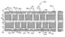
- the mid-plane 10is provided with a first side 12 and a second side 14 .
- the mid-plane 10is also provided with at least two multi-layer boards 16 , which are designated by the reference numeral 16 a and 16 b for purposes of clarity.
- Each of the multi-layer boards 16defines at least one and preferably more than one connector area 20 .
- the connector areas 20are designated for purposes of clarity by the referenced numerals 20 a , 20 b , 20 c and 20 d .
- the connector areas 20 a and 20 bare positioned adjacent to the first side 12 .
- the connector areas 20 c and 20 dare positioned adjacent to the second side 14 .
- the connector areas 20are designed to permit interconnection with connectors 22 such that the connectors 22 can be mounted on both sides, i.e., the first side 12 and the second side 14 , of the mid-plane 10 .
- the connectors 22are designated for purposes of clarity with the reference numerals 22 a , 22 b , 22 c , and 22 d .
- the connectors 22are connected to the multi-layer boards 16 by any suitable connection assembly 24 , which is illustrated in FIG. 1 by way of press fit connectors 26 by way of example. Only three of the press fit connectors 26 are labeled in FIG. 1 for purposes of clarity.
- the mid-plane 10is also provided with first and second metallic foils 30 and 32 .
- the first metallic foil 30is connected to the multi-layer board 16 a via a bonding material 34 .
- the second metallic foil 32is connected to the multi-layer board 16 b via a bonding material 36 .
- the multi-layer board 16 ais connected to the multi-layer board 16 b by way of a bonding material 38 .
- the bonding materials 34 , 36 and 38can be any suitable material capable of rigidly affixing the metallic foils 30 and 32 , and the multi-layer boards 16 a and 16 b together to form the mid-plane 10 as a rigid structure.
- the bonding materials 34 , 36 and 38can be an uncured pre-preg material.
- first and second metallic foils 30 and 32can be provided with predetermined conductive patterns thereon including vias or other types of electrical interconnections for connecting the first and second metallic foils 30 and 32 to the respective multi-layer boards 16 a and 16 b so that at least two independent circuits are formed on either side of the mid-plane 10 .
- the first metallic foil 30is electrically interconnected with the multi-layer board 16 a to form at least one independent circuit.
- the second metallic foil 32is interconnected with the multi-layer board 16 b to form at least one independent circuit.
- the circuits on the multi-layer boards 16 a and 16 bcan be interconnected, if desired, by vias or other suitable conductive paths formed in the mid-plane 10 .
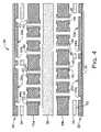
- FIGS. 2–5illustrate one method for forming the mid-plane 10 .
- FIGS. 2–5will now be described in more detail. However, it should be understood that other manners in constructing the mid-plane 10 can be used.
- the connection assembly 24 of the multi-layer board 16 aincludes a plurality of electrical connectors 40 defining a plurality of holes 42 .
- the connection assembly 24 of the multi-layer board 16 bis provided with a plurality of electrical connectors 46 defining a plurality of holes 48 .
- the electrical connectors 40 and 46are sized so that the holes 42 and 48 will matingly receive the press fit connectors 26 .
- the electrical connectors 40 and 46form a part of the connection assembly 24 referred to above in the preferred embodiment shown herein.
- the sizes of the holes 42 and 48are preferably equal to the pressfit sizes.
- the multi-layer boards 16 a and 16 bcan be characterized as buried via products complete with a surface finish (not shown) such as an ENIG finish.
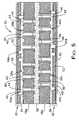
- the first and second metallic foils 30 and 32are substantially identical in construction and function. For purposes of brevity, only the first metallic foil 30 will be described in detail hereinafter.
- the first metallic foil 30is provided with a conductive layer 50 , and a dielectric layer 52 .
- the conductive layer 50is constructed of any type of suitable conductive material, such as aluminum, copper or the like. Typically, the conductive layer 50 will be constructed of copper.
- the conductive layer 50is etched or otherwise formed into the shape of a predetermined pattern for electrically connecting a variety of components and/or circuits provided in the multi-layer board 16 a .
- the dielectric layer 52can be constructed of any suitable type of dielectric material, such as FR4.
- the connector areas 20are defined in the dielectric layer 52 by creating a channel 54 about a perimeter of a connector area 20 .
- the channel 54is designated in FIG. 3 by the reference numerals 54 a , 54 b , 54 c and 54 d for purposes of clarity.
- the channels 54 a , 54 b , 54 c and 54 dserve at least two purposes.
- the first purposeis to prevent the bonding materials 34 and 36 from bleeding or flowing into the connector areas 20 a , 20 b , 20 c and 20 d .
- the other purposeis to permit removal of the first and second metallic foils 30 and 32 in the connector areas 20 a , 20 b , 20 c and 20 d in a subsequent manufacturing step, which will be discussed in more detail in FIG. 7 .
- the channels 54 a , 54 b , 54 c , and 54 dcan be formed in any suitable manner, such as with a router or a laser.
- the bonding materials 34 and 36are provided adjacent to the dielectric layer 52 and extend generally about the dielectric layer 52 , with the exception of the portions of the dielectric layer 52 provided in the connector areas 20 a , 20 b , 20 c and 20 d.
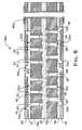
- FIG. 4Shown in FIG. 4 is a laminate stack 60 formed of the multi-layer boards 16 a and 16 b , first and second metallic foils 30 and 32 , and bonding materials 34 , 36 and 38 .
- the laminate stack 60is then subjected to conditions which causes the bonding materials 34 , 36 and 38 to bond the first and second metallic foils 30 and 32 , and the multi-layer boards 16 a and 16 b together, substantially as shown in FIG. 5 .
- the bonding materials 34 , 36 and 38are constructed of pre-preg
- the laminate stack 60is subjected to heat and pressure to form a rigid multi-layer 62 suitable for finishing.
- a rigid multi-layer 62 acan be produced, as shown in FIG. 6 .
- the rigid multi-layer 62 ais similar to the rigid multi-layer 62 except the conductive layer 50 has been removed and an electrical connector 40 a has been added.
- the rigid multi-layer 62 ais ready to be finished as standard. For example, drilling, plating, pattern outerlayers and surface finish may be utilized to finish the rigid multi-layer 62 a.
- the rigid multi-layer 62can be profiled in a well known manner, but first, the connector areas 22 a , 22 b , 22 c are opened to permit insertion of the connectors 22 a–b by cutting or removing materials adjacent to the channels 54 a–d .
- the depth toleranceis not critical because the first and second metallic foils 30 and 32 are pre-formed with the channels 54 a–d prior to formation of the rigid multi-layer 62 .
- the connector areas 22 a–dare opened by using depth control routing of the cambers.
- the mid plane 10can then be used in a well known manner. That is, the connectors 22 with the press fit connectors 26 are connected through the rigid multi-layer by inserting the press fit connectors 26 in through the holes 42 and 48 in the rigid multi-layer 62 .
- the use of mid planesis known in the art, and no more comments are believed necessary to teach one skilled in the art how to use the mid plane 10 in view of the other detailed description contained herein.
Landscapes
- Engineering & Computer Science (AREA)
- Microelectronics & Electronic Packaging (AREA)
- Manufacturing & Machinery (AREA)
- Combinations Of Printed Boards (AREA)
- Production Of Multi-Layered Print Wiring Board (AREA)
- Structure Of Printed Boards (AREA)
- Coupling Device And Connection With Printed Circuit (AREA)
- Chemical And Physical Treatments For Wood And The Like (AREA)
Abstract
Description
Claims (3)
Priority Applications (1)
| Application Number | Priority Date | Filing Date | Title |
|---|---|---|---|
| US10/887,484US7172805B2 (en) | 2003-07-08 | 2004-07-08 | Method for manufacturing a sequential backplane |
Applications Claiming Priority (2)
| Application Number | Priority Date | Filing Date | Title |
|---|---|---|---|
| US48576503P | 2003-07-08 | 2003-07-08 | |
| US10/887,484US7172805B2 (en) | 2003-07-08 | 2004-07-08 | Method for manufacturing a sequential backplane |
Publications (2)
| Publication Number | Publication Date |
|---|---|
| US20050109532A1 US20050109532A1 (en) | 2005-05-26 |
| US7172805B2true US7172805B2 (en) | 2007-02-06 |
Family
ID=33564053
Family Applications (2)
| Application Number | Title | Priority Date | Filing Date |
|---|---|---|---|
| US10/887,484Expired - Fee RelatedUS7172805B2 (en) | 2003-07-08 | 2004-07-08 | Method for manufacturing a sequential backplane |
| US10/564,215AbandonedUS20060278430A1 (en) | 2003-07-08 | 2004-07-08 | Method for manufacturing a midplane |
Family Applications After (1)
| Application Number | Title | Priority Date | Filing Date |
|---|---|---|---|
| US10/564,215AbandonedUS20060278430A1 (en) | 2003-07-08 | 2004-07-08 | Method for manufacturing a midplane |
Country Status (10)
| Country | Link |
|---|---|
| US (2) | US7172805B2 (en) |
| EP (1) | EP1647170B1 (en) |
| JP (1) | JP2007516593A (en) |
| CN (1) | CN100475012C (en) |
| AT (1) | ATE358411T1 (en) |
| AU (1) | AU2004300569A1 (en) |
| DE (1) | DE602004005598T2 (en) |
| ES (1) | ES2284031T3 (en) |
| PL (1) | PL1647170T3 (en) |
| WO (1) | WO2005004570A1 (en) |
Families Citing this family (6)
| Publication number | Priority date | Publication date | Assignee | Title |
|---|---|---|---|---|
| KR100665298B1 (en)* | 2004-06-10 | 2007-01-04 | 서울반도체 주식회사 | Light emitting device |
| FR3034219B1 (en) | 2015-03-23 | 2018-04-06 | Safran Electronics & Defense | BACKGROUND ELECTRONIC BOARD AND ELECTRONIC COMPUTER |
| DE102015113324A1 (en)* | 2015-08-12 | 2017-02-16 | Schweizer Electronic Ag | Ladder structure element with laminated inner layer substrate and method for its production |
| DE102015113322B3 (en) | 2015-08-12 | 2016-11-17 | Schweizer Electronic Ag | Radio-frequency antenna, radio-frequency substrate with radio-frequency antenna and method of production |
| US20170318673A1 (en)* | 2016-04-29 | 2017-11-02 | Arista Networks, Inc. | Connector for printed circuit board |
| FR3091136B1 (en)* | 2018-12-21 | 2022-01-21 | Safran Electronics & Defense | method of manufacturing a backplane electronic board |
Citations (25)
| Publication number | Priority date | Publication date | Assignee | Title |
|---|---|---|---|---|
| US3610811A (en)* | 1969-06-02 | 1971-10-05 | Honeywell Inf Systems | Printed circuit board with solder resist gas escape ports |
| US3756891A (en) | 1967-12-26 | 1973-09-04 | Multilayer circuit board techniques | |
| US4030190A (en) | 1976-03-30 | 1977-06-21 | International Business Machines Corporation | Method for forming a multilayer printed circuit board |
| GB2101411A (en) | 1981-06-04 | 1983-01-12 | Standard Telephones Cables Ltd | Flexi-rigid printed circuit boards |
| US4478469A (en)* | 1982-05-17 | 1984-10-23 | Zero Corporation | Card keying device |
| US4686607A (en) | 1986-01-08 | 1987-08-11 | Teradyne, Inc. | Daughter board/backplane assembly |
| US4943334A (en) | 1986-09-15 | 1990-07-24 | Compositech Ltd. | Method for making reinforced plastic laminates for use in the production of circuit boards |
| EP0438012A2 (en) | 1990-01-19 | 1991-07-24 | International Business Machines Corporation | Double-sided backplane assembly |
| US5199879A (en)* | 1992-02-24 | 1993-04-06 | International Business Machines Corporation | Electrical assembly with flexible circuit |
| US5400220A (en) | 1994-05-18 | 1995-03-21 | Dell Usa, L.P. | Mechanical printed circuit board and ball grid array interconnect apparatus |
| US5592737A (en) | 1991-06-04 | 1997-01-14 | Akzo Nobel N.V. | Method of manufacturing a multilayer printed wire board |
| US5690270A (en)* | 1993-11-08 | 1997-11-25 | Sawtek Inc. | Surface mounting stress relief device and method |
| US5826329A (en) | 1995-12-19 | 1998-10-27 | Ncr Corporation | Method of making printed circuit board using thermal transfer techniques |
| US5869356A (en) | 1996-05-29 | 1999-02-09 | International Business Machines Corporation | Method and structure for constraining the flow of incapsulant applied to an I/C chip on a substrate |
| US5904581A (en) | 1996-07-17 | 1999-05-18 | Minnesota Mining And Manufacturing Company | Electrical interconnection system and device |
| US6016598A (en) | 1995-02-13 | 2000-01-25 | Akzo Nobel N.V. | Method of manufacturing a multilayer printed wire board |
| US6174562B1 (en)* | 1996-07-09 | 2001-01-16 | Telefonaktiebolaget Lm Ericsson (Publ) | Method and device on printed boards |
| US6201305B1 (en)* | 2000-06-09 | 2001-03-13 | Amkor Technology, Inc. | Making solder ball mounting pads on substrates |
| US6456498B1 (en) | 2001-08-07 | 2002-09-24 | Hewlett-Packard Co. | CompactPCI-based computer system with mid-plane connector for equivalent front and back loading |
| US20020181217A1 (en) | 2001-06-01 | 2002-12-05 | Dorinel Patriche | Midplane for data processing apparatus |
| US6528737B1 (en) | 2000-08-16 | 2003-03-04 | Nortel Networks Limited | Midplane configuration featuring surface contact connectors |
| US6535397B2 (en) | 2001-05-31 | 2003-03-18 | Harris Corporation | Interconnect structure for interconnecting electronic modules |
| US6538899B1 (en) | 2001-01-02 | 2003-03-25 | Juniper Networks, Inc. | Traceless midplane |
| US6564450B2 (en)* | 1999-12-01 | 2003-05-20 | Leoni Bordnetz Sys Gmbh & Co | Contacting-making system for two printed circuit boards |
| US20040108137A1 (en) | 2002-12-10 | 2004-06-10 | Litton Systems, Inc. | Cross connect via for multilayer printed circuit boards |
Family Cites Families (3)
| Publication number | Priority date | Publication date | Assignee | Title |
|---|---|---|---|---|
| US5677515A (en)* | 1991-10-18 | 1997-10-14 | Trw Inc. | Shielded multilayer printed wiring board, high frequency, high isolation |
| KR100333627B1 (en)* | 2000-04-11 | 2002-04-22 | 구자홍 | Multi layer PCB and making method the same |
| US6499214B2 (en)* | 2000-05-26 | 2002-12-31 | Visteon Global Tech, Inc. | Method of making a circuit board |
- 2004
- 2004-07-08ATAT04744201Tpatent/ATE358411T1/ennot_activeIP Right Cessation
- 2004-07-08DEDE602004005598Tpatent/DE602004005598T2/ennot_activeExpired - Fee Related
- 2004-07-08JPJP2006518406Apatent/JP2007516593A/enactivePending
- 2004-07-08PLPL04744201Tpatent/PL1647170T3/enunknown
- 2004-07-08CNCNB2004800194092Apatent/CN100475012C/ennot_activeExpired - Fee Related
- 2004-07-08WOPCT/IB2004/002560patent/WO2005004570A1/enactiveIP Right Grant
- 2004-07-08AUAU2004300569Apatent/AU2004300569A1/ennot_activeAbandoned
- 2004-07-08USUS10/887,484patent/US7172805B2/ennot_activeExpired - Fee Related
- 2004-07-08USUS10/564,215patent/US20060278430A1/ennot_activeAbandoned
- 2004-07-08ESES04744201Tpatent/ES2284031T3/ennot_activeExpired - Lifetime
- 2004-07-08EPEP04744201Apatent/EP1647170B1/ennot_activeExpired - Lifetime
Patent Citations (29)
| Publication number | Priority date | Publication date | Assignee | Title |
|---|---|---|---|---|
| US3756891A (en) | 1967-12-26 | 1973-09-04 | Multilayer circuit board techniques | |
| US3610811A (en)* | 1969-06-02 | 1971-10-05 | Honeywell Inf Systems | Printed circuit board with solder resist gas escape ports |
| US4030190A (en) | 1976-03-30 | 1977-06-21 | International Business Machines Corporation | Method for forming a multilayer printed circuit board |
| GB2101411A (en) | 1981-06-04 | 1983-01-12 | Standard Telephones Cables Ltd | Flexi-rigid printed circuit boards |
| US4478469A (en)* | 1982-05-17 | 1984-10-23 | Zero Corporation | Card keying device |
| US4686607A (en) | 1986-01-08 | 1987-08-11 | Teradyne, Inc. | Daughter board/backplane assembly |
| US4943334A (en) | 1986-09-15 | 1990-07-24 | Compositech Ltd. | Method for making reinforced plastic laminates for use in the production of circuit boards |
| US5376326A (en) | 1986-09-15 | 1994-12-27 | Compositech Ltd. | Methods for making multilayer printed circuit boards |
| EP0438012A2 (en) | 1990-01-19 | 1991-07-24 | International Business Machines Corporation | Double-sided backplane assembly |
| EP0438012A3 (en) | 1990-01-19 | 1992-09-02 | International Business Machines Corporation | Double-sided backplane assembly |
| US5633072A (en) | 1991-06-04 | 1997-05-27 | Akzo Nobel N.V. | Method of manufacturing a multilayer printed wire board |
| US5592737A (en) | 1991-06-04 | 1997-01-14 | Akzo Nobel N.V. | Method of manufacturing a multilayer printed wire board |
| US5199879A (en)* | 1992-02-24 | 1993-04-06 | International Business Machines Corporation | Electrical assembly with flexible circuit |
| US5690270A (en)* | 1993-11-08 | 1997-11-25 | Sawtek Inc. | Surface mounting stress relief device and method |
| US5400220A (en) | 1994-05-18 | 1995-03-21 | Dell Usa, L.P. | Mechanical printed circuit board and ball grid array interconnect apparatus |
| US6016598A (en) | 1995-02-13 | 2000-01-25 | Akzo Nobel N.V. | Method of manufacturing a multilayer printed wire board |
| US5826329A (en) | 1995-12-19 | 1998-10-27 | Ncr Corporation | Method of making printed circuit board using thermal transfer techniques |
| US5869356A (en) | 1996-05-29 | 1999-02-09 | International Business Machines Corporation | Method and structure for constraining the flow of incapsulant applied to an I/C chip on a substrate |
| US6174562B1 (en)* | 1996-07-09 | 2001-01-16 | Telefonaktiebolaget Lm Ericsson (Publ) | Method and device on printed boards |
| US5904581A (en) | 1996-07-17 | 1999-05-18 | Minnesota Mining And Manufacturing Company | Electrical interconnection system and device |
| US6135781A (en) | 1996-07-17 | 2000-10-24 | Minnesota Mining And Manufacturing Company | Electrical interconnection system and device |
| US6564450B2 (en)* | 1999-12-01 | 2003-05-20 | Leoni Bordnetz Sys Gmbh & Co | Contacting-making system for two printed circuit boards |
| US6201305B1 (en)* | 2000-06-09 | 2001-03-13 | Amkor Technology, Inc. | Making solder ball mounting pads on substrates |
| US6528737B1 (en) | 2000-08-16 | 2003-03-04 | Nortel Networks Limited | Midplane configuration featuring surface contact connectors |
| US6538899B1 (en) | 2001-01-02 | 2003-03-25 | Juniper Networks, Inc. | Traceless midplane |
| US6535397B2 (en) | 2001-05-31 | 2003-03-18 | Harris Corporation | Interconnect structure for interconnecting electronic modules |
| US20020181217A1 (en) | 2001-06-01 | 2002-12-05 | Dorinel Patriche | Midplane for data processing apparatus |
| US6456498B1 (en) | 2001-08-07 | 2002-09-24 | Hewlett-Packard Co. | CompactPCI-based computer system with mid-plane connector for equivalent front and back loading |
| US20040108137A1 (en) | 2002-12-10 | 2004-06-10 | Litton Systems, Inc. | Cross connect via for multilayer printed circuit boards |
Also Published As
| Publication number | Publication date |
|---|---|
| DE602004005598D1 (en) | 2007-05-10 |
| US20050109532A1 (en) | 2005-05-26 |
| CN1820557A (en) | 2006-08-16 |
| EP1647170A1 (en) | 2006-04-19 |
| JP2007516593A (en) | 2007-06-21 |
| US20060278430A1 (en) | 2006-12-14 |
| CN100475012C (en) | 2009-04-01 |
| WO2005004570A1 (en) | 2005-01-13 |
| AU2004300569A1 (en) | 2005-01-13 |
| EP1647170B1 (en) | 2007-03-28 |
| DE602004005598T2 (en) | 2008-01-24 |
| ATE358411T1 (en) | 2007-04-15 |
| ES2284031T3 (en) | 2007-11-01 |
| PL1647170T3 (en) | 2007-08-31 |
Similar Documents
| Publication | Publication Date | Title |
|---|---|---|
| JP2631287B2 (en) | Manufacturing method of hybrid multilayer circuit board | |
| US9999134B2 (en) | Self-decap cavity fabrication process and structure | |
| JP2001326441A (en) | Composite wiring board and method of manufacturing the same | |
| US10321560B2 (en) | Dummy core plus plating resist restrict resin process and structure | |
| JP4246615B2 (en) | Flex-rigid printed wiring board and manufacturing method thereof | |
| US20170273195A1 (en) | Recessed cavity in printed circuit board protected by lpi | |
| US6802120B2 (en) | Method of manufacturing a printed wiring board having a non-through mounting hole | |
| US20120325531A1 (en) | Printed wiring board with improved corrosion resistance and yield | |
| US9992880B2 (en) | Rigid-bend printed circuit board fabrication | |
| US7172805B2 (en) | Method for manufacturing a sequential backplane | |
| US10772220B2 (en) | Dummy core restrict resin process and structure | |
| US6745463B1 (en) | Manufacturing method of rigid flexible printed circuit board | |
| JP3179572B2 (en) | Multilayer printed wiring board and method of manufacturing the same | |
| KR100335224B1 (en) | MDF multilayer board and its manufacturing method | |
| US8004851B2 (en) | Multi-layer flexible printed circuit board and manufacturing method thereof | |
| KR100722600B1 (en) | Method of forming through hole in multilayer printed circuit board | |
| CN215871951U (en) | circuit board assembly | |
| US20030131472A1 (en) | Method of fabricating a multi-layer circuit board assembly | |
| JPH0870183A (en) | Manufacture of multilayer printed-wiring board | |
| CN217591182U (en) | Soft and hard combined board of thick golden finger of branch tail ladder electricity | |
| US6739041B2 (en) | Circuit board and a method for making the same | |
| HK1093844A (en) | Method for manufacturing a midplane | |
| JPH0964542A (en) | Multilayered printed wiring board | |
| KR20020065261A (en) | ceramic piled components and method of manufacturing thereof | |
| JPH0750487A (en) | Multilayer printed wiring board |
Legal Events
| Date | Code | Title | Description |
|---|---|---|---|
| AS | Assignment | Owner name:VIASYSTEMS GROUP, INC., MISSOURI Free format text:ASSIGNMENT OF ASSIGNORS INTEREST;ASSIGNORS:HERMKENS, G.A.J.;THEELEN, ROGER;SMEETS, MARCEL;AND OTHERS;REEL/FRAME:023848/0044;SIGNING DATES FROM 20040830 TO 20040906 | |
| AS | Assignment | Owner name:VIASYSTEMS, INC.,MISSOURI Free format text:ASSIGNMENT OF ASSIGNORS INTEREST;ASSIGNOR:VIASYSTEMS GROUP, INC.;REEL/FRAME:023905/0147 Effective date:20100205 | |
| AS | Assignment | Owner name:WACHOVIA CAPITAL FINANCE CORPORATION (NEW ENGLAND) Free format text:SECURITY AGREEMENT;ASSIGNOR:VIASYSTEMS, INC.;REEL/FRAME:024062/0634 Effective date:20100216 | |
| REMI | Maintenance fee reminder mailed | ||
| LAPS | Lapse for failure to pay maintenance fees | ||
| STCH | Information on status: patent discontinuation | Free format text:PATENT EXPIRED DUE TO NONPAYMENT OF MAINTENANCE FEES UNDER 37 CFR 1.362 | |
| FP | Lapsed due to failure to pay maintenance fee | Effective date:20110206 | |
| AS | Assignment | Owner name:VIASYSTEMS, INC., MISSOURI Free format text:RELEASE BY SECURED PARTY;ASSIGNOR:WACHOVIA CAPITAL FINANCE CORPORATION (NEW ENGLAND);REEL/FRAME:035850/0669 Effective date:20150601 |