US7170807B2 - Data storage device and refreshing method for use with such device - Google Patents
Data storage device and refreshing method for use with such deviceDownload PDFInfo
- Publication number
- US7170807B2 US7170807B2US11/048,387US4838705AUS7170807B2US 7170807 B2US7170807 B2US 7170807B2US 4838705 AUS4838705 AUS 4838705AUS 7170807 B2US7170807 B2US 7170807B2
- Authority
- US
- United States
- Prior art keywords
- memory cell
- transistor
- electrical signals
- data state
- body region
- Prior art date
- Legal status (The legal status is an assumption and is not a legal conclusion. Google has not performed a legal analysis and makes no representation as to the accuracy of the status listed.)
- Expired - Lifetime, expires
Links
- 238000013500data storageMethods0.000titleabstractdescription28
- 238000000034methodMethods0.000titledescription13
- 230000015654memoryEffects0.000claimsabstractdescription73
- 239000004065semiconductorSubstances0.000claimsdescription26
- 230000004044responseEffects0.000claimsdescription17
- 210000000746body regionAnatomy0.000claims25
- 239000000969carrierSubstances0.000claims5
- 239000011159matrix materialSubstances0.000claims1
- 210000004027cellAnatomy0.000abstractdescription25
- 210000000352storage cellAnatomy0.000abstractdescription24
- 239000003990capacitorSubstances0.000description10
- 230000008569processEffects0.000description8
- 239000002800charge carrierSubstances0.000description4
- 230000000694effectsEffects0.000description3
- 230000005669field effectEffects0.000description3
- 238000005215recombinationMethods0.000description2
- 230000006798recombinationEffects0.000description2
- 230000007847structural defectEffects0.000description2
- 230000004075alterationEffects0.000description1
- 230000008901benefitEffects0.000description1
- 239000012212insulatorSubstances0.000description1
- 230000014759maintenance of locationEffects0.000description1
- 230000004048modificationEffects0.000description1
- 238000012986modificationMethods0.000description1
- 238000012634optical imagingMethods0.000description1
- 229910052710siliconInorganic materials0.000description1
- 239000010703siliconSubstances0.000description1
Images


Classifications
- G—PHYSICS
- G11—INFORMATION STORAGE
- G11C—STATIC STORES
- G11C11/00—Digital stores characterised by the use of particular electric or magnetic storage elements; Storage elements therefor
- G11C11/21—Digital stores characterised by the use of particular electric or magnetic storage elements; Storage elements therefor using electric elements
- G11C11/34—Digital stores characterised by the use of particular electric or magnetic storage elements; Storage elements therefor using electric elements using semiconductor devices
- G11C11/40—Digital stores characterised by the use of particular electric or magnetic storage elements; Storage elements therefor using electric elements using semiconductor devices using transistors
- G11C11/401—Digital stores characterised by the use of particular electric or magnetic storage elements; Storage elements therefor using electric elements using semiconductor devices using transistors forming cells needing refreshing or charge regeneration, i.e. dynamic cells
- G11C11/406—Management or control of the refreshing or charge-regeneration cycles
- G—PHYSICS
- G11—INFORMATION STORAGE
- G11C—STATIC STORES
- G11C11/00—Digital stores characterised by the use of particular electric or magnetic storage elements; Storage elements therefor
- G11C11/21—Digital stores characterised by the use of particular electric or magnetic storage elements; Storage elements therefor using electric elements
- G11C11/34—Digital stores characterised by the use of particular electric or magnetic storage elements; Storage elements therefor using electric elements using semiconductor devices
- G11C11/40—Digital stores characterised by the use of particular electric or magnetic storage elements; Storage elements therefor using electric elements using semiconductor devices using transistors
- G11C11/401—Digital stores characterised by the use of particular electric or magnetic storage elements; Storage elements therefor using electric elements using semiconductor devices using transistors forming cells needing refreshing or charge regeneration, i.e. dynamic cells
- G11C11/403—Digital stores characterised by the use of particular electric or magnetic storage elements; Storage elements therefor using electric elements using semiconductor devices using transistors forming cells needing refreshing or charge regeneration, i.e. dynamic cells with charge regeneration common to a multiplicity of memory cells, i.e. external refresh
- G11C11/404—Digital stores characterised by the use of particular electric or magnetic storage elements; Storage elements therefor using electric elements using semiconductor devices using transistors forming cells needing refreshing or charge regeneration, i.e. dynamic cells with charge regeneration common to a multiplicity of memory cells, i.e. external refresh with one charge-transfer gate, e.g. MOS transistor, per cell
- G—PHYSICS
- G11—INFORMATION STORAGE
- G11C—STATIC STORES
- G11C2211/00—Indexing scheme relating to digital stores characterized by the use of particular electric or magnetic storage elements; Storage elements therefor
- G11C2211/401—Indexing scheme relating to cells needing refreshing or charge regeneration, i.e. dynamic cells
- G11C2211/4016—Memory devices with silicon-on-insulator cells
- G—PHYSICS
- G11—INFORMATION STORAGE
- G11C—STATIC STORES
- G11C2211/00—Indexing scheme relating to digital stores characterized by the use of particular electric or magnetic storage elements; Storage elements therefor
- G11C2211/401—Indexing scheme relating to cells needing refreshing or charge regeneration, i.e. dynamic cells
- G11C2211/406—Refreshing of dynamic cells
- G11C2211/4065—Low level details of refresh operations
- G—PHYSICS
- G11—INFORMATION STORAGE
- G11C—STATIC STORES
- G11C2211/00—Indexing scheme relating to digital stores characterized by the use of particular electric or magnetic storage elements; Storage elements therefor
- G11C2211/401—Indexing scheme relating to cells needing refreshing or charge regeneration, i.e. dynamic cells
- G11C2211/406—Refreshing of dynamic cells
- G11C2211/4068—Voltage or leakage in refresh operations
- H—ELECTRICITY
- H01—ELECTRIC ELEMENTS
- H01L—SEMICONDUCTOR DEVICES NOT COVERED BY CLASS H10
- H01L2924/00—Indexing scheme for arrangements or methods for connecting or disconnecting semiconductor or solid-state bodies as covered by H01L24/00
- H01L2924/15—Details of package parts other than the semiconductor or other solid state devices to be connected
- H01L2924/151—Die mounting substrate
- H01L2924/153—Connection portion
- H01L2924/1531—Connection portion the connection portion being formed only on the surface of the substrate opposite to the die mounting surface
- H01L2924/15311—Connection portion the connection portion being formed only on the surface of the substrate opposite to the die mounting surface being a ball array, e.g. BGA
Definitions
- the present inventionrelates to a data storage device, and relates particularly, but not exclusively, to a semiconductor memory device.
- the inventionalso relates to a method of refreshing a data storage device.
- DRAMDynamic Random Access Memory
- each storage cellconsisting of a single transistor and a single capacitor.
- each storage cellstores a single binary data bit according to whether the associated capacitor is charged (data state “1”) or discharged (data state “0”). It is also well known that the charge stored in the charged capacitors decays with time, and that it is therefore necessary to rewrite the data to the charged storage cells by periodically recharging the capacitors.
- a conventional DRAM arrangement of this typeis shown in FIG. 1 .
- the DRAM device shown in FIG. 1is provided with m columns and n rows.
- a data storage cell 10consisting of a single transistor and a single capacitor is located at each intersection of a row and a column.
- the source of the associated transistoris connected to one terminal of a capacitor, the other terminal of which is connected to a ground terminal or a given reference voltage (not shown), the gates of the transistors of each row are connected together by a respective conductive track 12 , and the drains of the transistors of each column are connected together by a respective conductive track 14 .
- Each of the conductive tracks 12is connected to a selection circuit 16 for sequentially scanning the conductive tracks 12 of the memory device, and the conductive tracks 14 are each connected to respective writing circuits 18 i and reading circuits 20 i , where i varies from 1 to m.
- the selection circuit 16scans lines 1 to n by sequentially applying a signal to each conductive track 12 to successively switch on the transistors of all of the data storage cells 10 connected to the conductive track 12 being addressed. This in turn enables the reading circuits 20 i to determine the charge state of the associated capacitor by determining the current flowing through each transistor. In response to the determination of the charge state of each capacitor determined by the associated reading circuit 20 i , the associated writing circuit 18 i causes the capacitor to be recharged or not, depending on its previous charge state.
- Prior art DRAM devices of the type shown in FIG. 1suffer from the drawback that modern memory devices have capacities typically of the order of 1 Gb, such devices typically comprising 1048576 lines.
- the refreshing processtypically requires 10 to 50 ns for each line, as a result of which the refreshing process for a 1 Gb device typically requires 10 to 50 ms. Since the refreshing process must typically be carried out about 10 times per second, the time necessary for the refreshing process is of the same order of magnitude as that remaining for the data reading and writing operations. This results in the time required for refreshing limiting the capacity of the memory devices and requiring that special steps be taken to reduce leakage currents.
- Preferred embodiments of the present inventionseek to overcome the above disadvantages of the prior art.
- a data storage devicecomprising:
- each said cellhaving a physical parameter in use which varies with time and has one of two data representing states, each said data representing state representing a respective binary logic state;
- refreshing meansfor applying input signals to each said data storage cell to at least partially reverse variation of said physical parameter with time of at least those data storage cells in a predetermined one of said states, wherein said input signals cause a different variation in said physical parameter in cells in one of said data representing states than the variation caused in cells in the other of said data representing states.
- Data refreshing meansare provided to at least partially reverse the variation of said physical parameter with time by means of input signals causing a different variation in said physical parameter in cells in one of said data representing states than the variation caused in cells in the other of said data representing states.
- said at least partial reversal of said physical parameteroccurs to a greater extent for said cells in said predetermined one of said data representing states than in the other of said states, and said input signals are applied sufficiently frequently in use that said states remain distinguishable from each other.
- the devicemay further comprise writing means for applying input signals to each said data storage cell to adjust said physical parameter of said cell to select the binary logic state represented by each said data storage cell.
- the devicemay further comprise reading means for determining the data representing state of each said data storage cell.
- Said input signalsmay at least partially reverse variation of said physical parameter for cells in each of said data representing states.
- the data storage devicemay be a semiconductor device.
- At least some of said data storage cellseach comprise a respective field effect transistor having a first threshold voltage when in said first state and a second threshold voltage when in said second state.
- At least one said field effect transistorcomprises a respective source, a respective drain, a respective body arranged between the corresponding said source and said drain and adapted to retain an electrical charge generated in said body representing one or the other of two binary data states, and at least one respective gate adjacent the corresponding said body, wherein said refreshing means is adapted to apply voltage signals between at least one said gate and said drain of each said cell lying between said first and second threshold voltages.
- Said refreshing meansmay be adapted to also apply signals to at least partially reverse the variation of said physical parameter in the other of said data representing states.
- Said refreshing meansis preferably adapted to apply signals partially reversing the variation of said charge in the other of said data representing states by means of recombination of charge carriers with charge carriers of opposite polarity.
- the devicemay be a memory device.
- a method of refreshing data in a data storage devicecomprising a plurality of data storage cells, each said cell having a physical parameter in use which varies with time and has one of two data representing states, each said data representing state representing a respective binary logic state, the method comprising applying input signals to each said data storage cell to at least partially reverse variation of said physical parameter with time of at least those data storage cells in a predetermined one of said states, wherein said input signals cause a different variation in said physical parameter in cells in one of said data representing states than the variation caused in cells in the other of said data representing states.
- Said input signalsmay cause said at least partial reversal of said physical parameter occurs to a greater extent for said cells in said predetermined one of said data representing states than in the other of said states.
- the methodmay further comprise the step of applying signals to at least partially reverse the variation of said physical parameter in the other of said data representing states.
- the step of applying signals to at least partially reverse the variation of said physical parameter in the other of said data representing statespreferably causes recombination of charge carriers with charge carriers of opposite polarity.
- Said input signalsmay at least partially reverse variation of said physical parameter for cells in each of said data representing states.
- FIG. 1is a schematic representation of a prior art DRAM memory device
- FIG. 2is a schematic representation, corresponding to FIG. 1 , of a DRAM device embodying the present invention
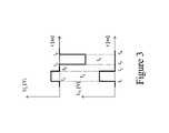
- FIG. 3shows a pulse pattern to be applied to the gates and drains of the transistors of the device of FIG. 2 during a refresh operation
- FIG. 4shows the variation of charge with time in the body of each transistor of the device of FIG. 2 in each of the two charge states.
- a DRAM devicehas an array of m columns and n lines of memory cells 10 , each of which comprises an NMOS SOI (silicon on insulator) field effect transistor, as described in greater detail in European patent application number 01810587.4 (which corresponds, at least in part, to U.S. Pat. No. 6,969.662).
- NMOS SOIsilicon on insulator
- a positive chargeis generated and stored in the body of an NMOS transistor by means of the application of a voltage between the source and drain of the transistor when in its conductive state, the voltage difference between the source and drain generating electron-hole pairs by impact ionisation.
- the electronsare then removed to the source or drain, and the holes are stored in the body of the transistor.
- the positive chargecan be removed by forward biasing the body-drain junction.
- the source of each transistoris connected to a ground terminal
- the gates of the transistors of each lineare connected to a conductive track 12
- the drains of the transistors of each columnare connected to a conductive track 14 .
- the conductive tracks 12are all connected to a selection circuit 16
- a writing circuit 18 i and reading circuit 20 iis connected to each conducting track 14 .
- a refreshing circuit 22is also provided, the refreshing circuit 22 being connected to each of the conductive tracks 12 via the selection circuit, and to each of the conductive tracks 14 via the corresponding writing circuits 18 i.
- European patent application no. 01810587.4describes how data can be written to the individual memory cells 10 of the DRAM device of FIG. 2 , and how the charge state, representing the binary data state, of each memory cell 10 can be determined.
- the “zero” and “one” binary states of each stored bitare represented by the presence or absence of a net electric charge of a predetermined polarity in the body of the transistor.
- the refreshing circuit 22causes the selection circuit 16 and writing circuit 18 i to apply pulse in to all of the lines, and pulse 12 , as shown in FIG. 3 , to all of the columns.
- Pulse I 1 beginning at time t 1 and ending at time t 2is applied to the gates of all of the transistors for a duration of some nanoseconds, and comprises a pulse of +0.6V applied to the gates, and +1.2V applied to the drains of the transistors.
- Pulse I 2which begins at time t 3 and ends at time t 4 , also having a duration of some nanoseconds, consists of the application of a pulse of ⁇ 2V to the gates alone. The times t 2 and t 3 may be coincident.
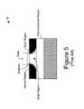
- FIG. 4which shows in detail how the charge C stored in the transistor body of each memory cell 10 varies with time for each charge state (representing binary “0” and binary “1” states respectively), the line between the two curves indicates charge level C n towards which both charge levels tend if no refreshing operation is carried out. It will be appreciated that the two charge levels chosen to represent the respective data states must be sufficiently far apart as to remain distinguishable from each other throughout the range of allowed variation of charge of each level.
- the cells 10initially have a net positive charge represented by holes stored in the body of the transistor (representing state “1”) or a much lower negative or substantially zero charge (representing state “0”), i.e. the two charged states being higher than or lower than charge level C n respectively. Without a refresh operation, the difference between these two charge levels decays generally logarithmically with time.
- the electrical properties of the SOI MOSFET transistors of each data storage cell 10vary according to the amount of charge stored in the body of the respective transistor.
- the threshold voltage of transistors in the higher charge stateis lower than that of the transistors in the lower charge state.
- the voltage applied to the gatesis arranged to be between the respective threshold voltages of the transistors in the higher and lower charge states.
- the transistor in the higher charge stateis switched to its conductive state, i.e. a conductive channel between the source and drain forms in the body of the transistor in the vicinity of the gate, and a current can flow in the channel between the source and the drain at the interface of the body and the insulating layer adjacent the gate. This current flowing in the channel creates electron and hole pairs in the vicinity of the drain by impact ionisation, the holes being stored in the body, while the electrons are removed by the drain.
- ⁇ 1is generally 2 to 3 orders of magnitude greater than ⁇ 2. It is found that electrons are trapped in structural defects in the body at its interface with the insulating film between the body and the gate generally to the same extent, regardless of whether the transistors are in the higher or lower charge state.
- the second pulse I 2begins and causes the charge in the transistors of both charge states to be reduced.
- the pulse 12consists of a voltage of ⁇ 2V applied to the gates, which attracts holes stored in the body of each transistor to the corresponding interface of the body and dielectric film, with the result that the holes recombine with electrons trapped in structural defects at the interface, reducing the net positive charge stored in the body.
- FIG. 4in this way, the charge in the higher state is reduced back to its initial level, and the charge in the lower state is restored to its previous level.
- the charge in the transistor in the upper stateis reduced by ⁇ 4, and is reduced by ⁇ 3 in the transistor in the lower state, ⁇ 4 and ⁇ 3 being approximately equal to each other.
- pulse I 1has a much more significant effect on transistors in the higher state than in the lower state
- this pulsecan be applied to all of the memory cells 10 simultaneously, with the effect that the “1” states are refreshed, without the transistors in the “0” state being converted to the “1” state and without the necessity of reading the charge state of each memory cell 10 .
Landscapes
- Engineering & Computer Science (AREA)
- Microelectronics & Electronic Packaging (AREA)
- Computer Hardware Design (AREA)
- Dram (AREA)
Abstract
Description
Claims (24)
Priority Applications (2)
| Application Number | Priority Date | Filing Date | Title |
|---|---|---|---|
| US11/048,387US7170807B2 (en) | 2002-04-18 | 2005-02-01 | Data storage device and refreshing method for use with such device |
| US11/649,945US7342842B2 (en) | 2002-04-18 | 2007-01-05 | Data storage device and refreshing method for use with such device |
Applications Claiming Priority (9)
| Application Number | Priority Date | Filing Date | Title |
|---|---|---|---|
| EP02405314.2 | 2002-04-18 | ||
| EP02405314 | 2002-04-18 | ||
| EP02405314AEP1355317A1 (en) | 2002-04-18 | 2002-04-18 | Memory refreshing device |
| EP02077116 | 2002-05-29 | ||
| EP02077116.8 | 2002-05-29 | ||
| EP02077116AEP1355316B1 (en) | 2002-04-18 | 2002-05-29 | Data storage device and refreshing method for use with such device |
| PCT/EP2003/002747WO2003088255A1 (en) | 2002-04-18 | 2003-03-17 | Data storage device and refreshing method for use with such device |
| US10/487,162US6982918B2 (en) | 2002-04-18 | 2003-03-17 | Data storage device and refreshing method for use with such device |
| US11/048,387US7170807B2 (en) | 2002-04-18 | 2005-02-01 | Data storage device and refreshing method for use with such device |
Related Parent Applications (3)
| Application Number | Title | Priority Date | Filing Date |
|---|---|---|---|
| PCT/EP2003/002747DivisionWO2003088255A1 (en) | 2002-04-18 | 2003-03-17 | Data storage device and refreshing method for use with such device |
| US10/487,162DivisionUS6982918B2 (en) | 2002-04-18 | 2003-03-17 | Data storage device and refreshing method for use with such device |
| US10487162Division | 2003-03-17 |
Related Child Applications (1)
| Application Number | Title | Priority Date | Filing Date |
|---|---|---|---|
| US11/649,945DivisionUS7342842B2 (en) | 2002-04-18 | 2007-01-05 | Data storage device and refreshing method for use with such device |
Publications (2)
| Publication Number | Publication Date |
|---|---|
| US20050128851A1 US20050128851A1 (en) | 2005-06-16 |
| US7170807B2true US7170807B2 (en) | 2007-01-30 |
Family
ID=28676391
Family Applications (3)
| Application Number | Title | Priority Date | Filing Date |
|---|---|---|---|
| US10/487,162Expired - LifetimeUS6982918B2 (en) | 2002-04-18 | 2003-03-17 | Data storage device and refreshing method for use with such device |
| US11/048,387Expired - LifetimeUS7170807B2 (en) | 2002-04-18 | 2005-02-01 | Data storage device and refreshing method for use with such device |
| US11/649,945Expired - LifetimeUS7342842B2 (en) | 2002-04-18 | 2007-01-05 | Data storage device and refreshing method for use with such device |
Family Applications Before (1)
| Application Number | Title | Priority Date | Filing Date |
|---|---|---|---|
| US10/487,162Expired - LifetimeUS6982918B2 (en) | 2002-04-18 | 2003-03-17 | Data storage device and refreshing method for use with such device |
Family Applications After (1)
| Application Number | Title | Priority Date | Filing Date |
|---|---|---|---|
| US11/649,945Expired - LifetimeUS7342842B2 (en) | 2002-04-18 | 2007-01-05 | Data storage device and refreshing method for use with such device |
Country Status (5)
| Country | Link |
|---|---|
| US (3) | US6982918B2 (en) |
| EP (1) | EP1355316B1 (en) |
| CN (1) | CN100466098C (en) |
| AU (1) | AU2003215662A1 (en) |
| WO (1) | WO2003088255A1 (en) |
Cited By (330)
| Publication number | Priority date | Publication date | Assignee | Title |
|---|---|---|---|---|
| US20060186457A1 (en)* | 2005-02-18 | 2006-08-24 | Burnett James D | Methods for programming a floating body nonvolatile memory |
| US20060186456A1 (en)* | 2005-02-18 | 2006-08-24 | Burnett James D | NVM cell on SOI and method of manufacture |
| US20070257291A1 (en)* | 2006-05-02 | 2007-11-08 | Serguei Okhonin | Semiconductor memory cell and array using punch-through to program and read same |
| US20070297252A1 (en)* | 2006-06-26 | 2007-12-27 | Anant Pratap Singh | Integrated circuit having memory array including ECC and/or column redundancy, and method of programming, controlling and/or operating same |
| US20080061631A1 (en)* | 2006-08-28 | 2008-03-13 | Fouquet Julie E | Galvanic isolator |
| US20080180206A1 (en)* | 2006-08-28 | 2008-07-31 | Avago Technologies Ecbu (Singapore) Pte.Ltd. | Coil Transducer with Reduced Arcing and Improved High Voltage Breakdown Performance Characteristics |
| US20080180995A1 (en)* | 2007-01-26 | 2008-07-31 | Serguei Okhonin | Semiconductor Device With Electrically Floating Body |
| US20080237714A1 (en)* | 2007-03-29 | 2008-10-02 | Pierre Fazan | Manufacturing Process for Zero-Capacitor Random Access Memory Circuits |
| US20080278275A1 (en)* | 2007-05-10 | 2008-11-13 | Fouquet Julie E | Miniature Transformers Adapted for use in Galvanic Isolators and the Like |
| US20080298139A1 (en)* | 2007-05-30 | 2008-12-04 | David Fisch | Integrated circuit having voltage generation circuitry for memory cell array, and method of operating and /or controlling same |
| US20080316849A1 (en)* | 2007-06-22 | 2008-12-25 | Kabushiki Kaisha Toshiba | Memory driving method and semiconductor storage device |
| US20090016118A1 (en)* | 2007-07-12 | 2009-01-15 | Silicon Storage Technology, Inc. | Non-volatile dram with floating gate and method of operation |
| US20090022003A1 (en)* | 2007-07-20 | 2009-01-22 | Song Ki-Whan | Memory cell structures, memory arrays, memory devices, memory controllers, and memory systems, and methods of manufacturing and operating the same |
| WO2009039169A1 (en)* | 2007-09-17 | 2009-03-26 | Innovative Silicon S.A. | Refreshing data of memory cells with electrically floating body transistors |
| US20090078999A1 (en)* | 2007-09-20 | 2009-03-26 | Anderson Brent A | Semiconductor device structures with floating body charge storage and methods for forming such semiconductor device structures. |
| US20090086559A1 (en)* | 2007-10-02 | 2009-04-02 | Kabushiki Kaisha Toshiba | Semiconductor memory device and driving method thereof |
| US20090097332A1 (en)* | 2007-10-10 | 2009-04-16 | Samsung Electronics Co., Ltd. | Semiconductor memory device |
| US20090108292A1 (en)* | 2007-10-26 | 2009-04-30 | Jun Liu | Floating Body Field-Effect Transistors, and Methods of Forming Floating Body Field-Effect Transistors |
| US20090141550A1 (en)* | 2006-04-07 | 2009-06-04 | Eric Carman | Memory Array Having a Programmable Word Length, and Method of Operating Same |
| US20090146219A1 (en)* | 2007-12-11 | 2009-06-11 | Danngis Liu | Integrated circuit having memory cell array, and method of manufacturing same |
| US20090200612A1 (en)* | 2008-02-08 | 2009-08-13 | Viktor Koldiaev | Integrated Circuit Having Memory Cells Including Gate Material Having High Work Function, and Method of Manufacturing Same |
| US20090206817A1 (en)* | 2008-02-15 | 2009-08-20 | Avago Technologies Ecbu (Singapore) Ple. Ltd. | High Voltage Drive Circuit Employing Capacitive Signal Coupling and Associated Devices and Methods |
| US20090206958A1 (en)* | 2008-02-15 | 2009-08-20 | Avago Technologies Ecbu (Singapore) Pte. Ltd. | High Voltage Isolation Semiconductor Capacitor Digital Communication Device and Corresponding Package |
| US20090206960A1 (en)* | 2008-02-15 | 2009-08-20 | Avago Technologies Ecbu (Singapore) Pte Ltd. | High Voltage Isolation Dual Capacitor Communication System |
| US20090231898A1 (en)* | 2006-07-11 | 2009-09-17 | David Fisch | Integrated Circuit Including Memory Array Having a Segmented Bit Line Architecture and Method of Controlling and/or Operating Same |
| US20090243783A1 (en)* | 2006-08-28 | 2009-10-01 | Avago Technologies Ecbu (Singapore) Pte. Ltd. | Minimizing Electromagnetic Interference in Coil Transducers |
| US20090243782A1 (en)* | 2006-08-28 | 2009-10-01 | Avago Technologies Ecbu (Singapore) Pte. Ltd. | High Voltage Hold-Off Coil Transducer |
| US20090251958A1 (en)* | 2008-04-04 | 2009-10-08 | Philippe Bauser | Read circuitry for an integrated circuit having memory cells and/or a memory cell array, and method of operating same |
| US20090278194A1 (en)* | 2008-05-06 | 2009-11-12 | Nam-Kyun Tak | Capacitorless one-transistor semiconductor memory device having improved data retention abilities and operation characteristics |
| US20090316492A1 (en)* | 2007-11-29 | 2009-12-24 | Yuniarto Widjaja | Memory cells, memory cell arrays, methods of using and methods of making |
| US20100020448A1 (en)* | 2006-08-28 | 2010-01-28 | Avago Technologies Ecbu Ip (Singapore) Pte. Ltd. | Galvanic isolator |
| US20100034041A1 (en)* | 2008-08-05 | 2010-02-11 | Yuniarto Widjaja | Method of operating semiconductor memory device with floating body transistor using silicon controlled rectifier principle |
| US20100046287A1 (en)* | 2008-08-22 | 2010-02-25 | Yuniarto Widjaja | Semiconductor memory having both volatile and non-volatile functionality including resistance change material and method of operating |
| US20100075471A1 (en)* | 2008-09-25 | 2010-03-25 | Innovative Silicon Isi Sa | Recessed Gate Silicon-On-Insulator Floating Body Device With Self-Aligned Lateral Isolation |
| US20100085806A1 (en)* | 2008-10-02 | 2010-04-08 | Ping Wang | Techniques for reducing a voltage swing |
| US20100091586A1 (en)* | 2008-10-15 | 2010-04-15 | Innovative Silicon Isi Sa | Techniques for simultaneously driving a plurality of source lines |
| US20100110816A1 (en)* | 2008-11-05 | 2010-05-06 | Innovative Silicon Isi Sa | Techniques for block refreshing a semiconductor memory device |
| US20100149886A1 (en)* | 2008-12-17 | 2010-06-17 | Samsung Electronics Co., Ltd. | Semiconductor memory device and method for operating the same |
| US20100159650A1 (en)* | 2008-12-18 | 2010-06-24 | Song Ho-Ju | Methods of fabricating semiconductor device having capacitorless one-transistor memory cell |
| US20100188182A1 (en)* | 2006-08-28 | 2010-07-29 | Avago Technologies Ecbu (Singapore) Pte.Ltd. | Narrowbody Coil Isolator |
| US20100210075A1 (en)* | 2009-02-18 | 2010-08-19 | Innovative Silicon Isi Sa | Techniques for providing a source line plane |
| US20100224924A1 (en)* | 2009-03-04 | 2010-09-09 | Innovative Silicon Isi Sa | Techniques for forming a contact to a buried diffusion layer in a semiconductor memory device |
| US20100246284A1 (en)* | 2007-11-29 | 2010-09-30 | Yuniarto Widjaja | Semiconductor memory having electrically floating body transistor |
| US20100246277A1 (en)* | 2007-11-29 | 2010-09-30 | Yuniarto Widjaja | Method of maintaining the state of semiconductor memory having electrically floating body transistor |
| US20100259909A1 (en)* | 2006-08-28 | 2010-10-14 | Avago Technologies Ecbu (Singapore) Pte. Ltd. | Widebody Coil Isolators |
| US20100259964A1 (en)* | 2009-03-31 | 2010-10-14 | Innovative Silicon Isi Sa | Techniques for providing a semiconductor memory device |
| US20100260003A1 (en)* | 2009-04-14 | 2010-10-14 | Young Hoon Oh | Semiconductor memory apparatus and refresh control method of the same |
| US20100271858A1 (en)* | 2009-04-27 | 2010-10-28 | Innovative Silicon Isi Sa | Techniques for providing a direct injection semiconductor memory device having ganged carrier injection lines |
| US20100277982A1 (en)* | 2009-04-30 | 2010-11-04 | Innovative Silicon Isi Sa | Semiconductor device with floating gate and electrically floating body |
| US7839711B2 (en) | 2008-01-16 | 2010-11-23 | Kabushiki Kaisha Toshiba | Semiconductor memory device and driving method thereof |
| US20100328902A1 (en)* | 2009-06-30 | 2010-12-30 | Avago Technologies Ecbu Ip (Singapore) Pte. Ltd. | Coil Transducer Isolator Packages |
| US20110007578A1 (en)* | 2009-07-10 | 2011-01-13 | Innovative Silicon Isi Sa | Techniques for providing a semiconductor memory device |
| US20110019479A1 (en)* | 2009-07-27 | 2011-01-27 | Innovative Silicon Isi Sa | Techniques for providing a direct injection semiconductor memory device |
| US20110031997A1 (en)* | 2009-04-14 | 2011-02-10 | NuPGA Corporation | Method for fabrication of a semiconductor device and structure |
| US20110044110A1 (en)* | 2007-10-24 | 2011-02-24 | Yuniarto Widjaja | Semiconductor memory having both volatile and non-volatile functionality and method of operating |
| US20110049577A1 (en)* | 2009-04-14 | 2011-03-03 | NuPGA Corporation | System comprising a semiconductor device and structure |
| US20110058436A1 (en)* | 2009-09-04 | 2011-03-10 | Innovative Silicon Isi Sa | Techniques for sensing a semiconductor memory device |
| US20110084314A1 (en)* | 2009-10-12 | 2011-04-14 | NuPGA Corporation | System comprising a semiconductor device and structure |
| US20110092030A1 (en)* | 2009-04-14 | 2011-04-21 | NuPGA Corporation | System comprising a semiconductor device and structure |
| US20110095620A1 (en)* | 2006-08-28 | 2011-04-28 | Avago Technologies Ecbu (Singapore) Pte. Ltd. | Galvanic Isolators and Coil Transducers |
| US20110108888A1 (en)* | 2009-04-14 | 2011-05-12 | NuPGA Corporation | System comprising a semiconductor device and structure |
| US20110121366A1 (en)* | 2009-04-14 | 2011-05-26 | NuPGA Corporation | System comprising a semiconductor device and structure |
| US20110141836A1 (en)* | 2009-12-16 | 2011-06-16 | Innovative Silicon Isi Sa | Techniques for reducing impact of array disturbs in a semiconductor memory device |
| WO2011097592A1 (en) | 2010-02-07 | 2011-08-11 | Zeno Semiconductor , Inc. | Semiconductor memory device having electrically floating body transistor, and having both volatile and non-volatile functionality and method |
| US20110199848A1 (en)* | 2010-02-12 | 2011-08-18 | Innovative Silicon Isi Sa | Techniques for controlling a semiconductor memory device |
| CN102169714A (en)* | 2010-02-25 | 2011-08-31 | 复旦大学 | Method for refreshing bulk-silicon floating body cell transistor memory |
| US8014195B2 (en) | 2008-02-06 | 2011-09-06 | Micron Technology, Inc. | Single transistor memory cell |
| US20110216617A1 (en)* | 2010-03-04 | 2011-09-08 | Innovative Silicon Isi Sa | Techniques for sensing a semiconductor memory device |
| US20110216608A1 (en)* | 2010-03-05 | 2011-09-08 | Innovative Silicon Isi Sa | Techniques for reading from and/or writing to a semiconductor memory device |
| US20110216605A1 (en)* | 2010-03-04 | 2011-09-08 | Innovative Silicon Isi Sa | Techniques for providing a semiconductor memory device having hierarchical bit lines |
| US8085594B2 (en) | 2007-06-01 | 2011-12-27 | Micron Technology, Inc. | Reading technique for memory cell with electrically floating body transistor |
| WO2011140033A3 (en)* | 2010-05-06 | 2012-01-19 | Micron Technology, Inc. | Techniques for refreshing a semiconductor memory device |
| US8163581B1 (en) | 2010-10-13 | 2012-04-24 | Monolith IC 3D | Semiconductor and optoelectronic devices |
| US8174886B2 (en) | 2007-11-29 | 2012-05-08 | Zeno Semiconductor, Inc. | Semiconductor memory having electrically floating body transistor |
| US8174881B2 (en) | 2009-11-24 | 2012-05-08 | Micron Technology, Inc. | Techniques for reducing disturbance in a semiconductor device |
| US8194471B2 (en) | 2010-10-04 | 2012-06-05 | Zeno Semiconductor, Inc. | Semiconductor memory device having an electrically floating body transistor |
| US8203148B2 (en) | 2010-10-11 | 2012-06-19 | Monolithic 3D Inc. | Semiconductor device and structure |
| US8213226B2 (en) | 2008-12-05 | 2012-07-03 | Micron Technology, Inc. | Vertical transistor memory cell and array |
| US8258810B2 (en) | 2010-09-30 | 2012-09-04 | Monolithic 3D Inc. | 3D semiconductor device |
| US8258911B2 (en) | 2008-03-31 | 2012-09-04 | Avago Technologies ECBU IP (Singapor) Pte. Ltd. | Compact power transformer components, devices, systems and methods |
| US8264876B2 (en) | 2010-10-04 | 2012-09-11 | Zeno Semiconductor, Inc. | Semiconductor memory device having an electrically floating body transistor |
| US8273610B2 (en) | 2010-11-18 | 2012-09-25 | Monolithic 3D Inc. | Method of constructing a semiconductor device and structure |
| US8283215B2 (en) | 2010-10-13 | 2012-10-09 | Monolithic 3D Inc. | Semiconductor and optoelectronic devices |
| US8294159B2 (en) | 2009-10-12 | 2012-10-23 | Monolithic 3D Inc. | Method for fabrication of a semiconductor device and structure |
| US8298875B1 (en) | 2011-03-06 | 2012-10-30 | Monolithic 3D Inc. | Method for fabrication of a semiconductor device and structure |
| US8362800B2 (en) | 2010-10-13 | 2013-01-29 | Monolithic 3D Inc. | 3D semiconductor device including field repairable logics |
| US8373230B1 (en) | 2010-10-13 | 2013-02-12 | Monolithic 3D Inc. | Method for fabrication of a semiconductor device and structure |
| US8373439B2 (en) | 2009-04-14 | 2013-02-12 | Monolithic 3D Inc. | 3D semiconductor device |
| US8378715B2 (en) | 2009-04-14 | 2013-02-19 | Monolithic 3D Inc. | Method to construct systems |
| US8379458B1 (en) | 2010-10-13 | 2013-02-19 | Monolithic 3D Inc. | Semiconductor device and structure |
| US8378494B2 (en) | 2009-04-14 | 2013-02-19 | Monolithic 3D Inc. | Method for fabrication of a semiconductor device and structure |
| US8384426B2 (en) | 2009-04-14 | 2013-02-26 | Monolithic 3D Inc. | Semiconductor device and structure |
| US8391066B2 (en) | 2006-11-29 | 2013-03-05 | Zeno Semiconductor, Inc. | Semiconductor memory having both volatile and non-volatile functionality and method of operating |
| US8427200B2 (en) | 2009-04-14 | 2013-04-23 | Monolithic 3D Inc. | 3D semiconductor device |
| US8440542B2 (en) | 2010-10-11 | 2013-05-14 | Monolithic 3D Inc. | Semiconductor device and structure |
| US8450804B2 (en) | 2011-03-06 | 2013-05-28 | Monolithic 3D Inc. | Semiconductor device and structure for heat removal |
| US8461035B1 (en) | 2010-09-30 | 2013-06-11 | Monolithic 3D Inc. | Method for fabrication of a semiconductor device and structure |
| US8476145B2 (en) | 2010-10-13 | 2013-07-02 | Monolithic 3D Inc. | Method of fabricating a semiconductor device and structure |
| US8492886B2 (en) | 2010-02-16 | 2013-07-23 | Monolithic 3D Inc | 3D integrated circuit with logic |
| US8498157B2 (en) | 2009-05-22 | 2013-07-30 | Micron Technology, Inc. | Techniques for providing a direct injection semiconductor memory device |
| US8514622B2 (en) | 2007-11-29 | 2013-08-20 | Zeno Semiconductor, Inc. | Compact semiconductor memory device having reduced number of contacts, methods of operating and methods of making |
| US8531878B2 (en) | 2011-05-17 | 2013-09-10 | Micron Technology, Inc. | Techniques for providing a semiconductor memory device |
| US8536628B2 (en) | 2007-11-29 | 2013-09-17 | Micron Technology, Inc. | Integrated circuit having memory cell array including barriers, and method of manufacturing same |
| US8536023B2 (en) | 2010-11-22 | 2013-09-17 | Monolithic 3D Inc. | Method of manufacturing a semiconductor device and structure |
| US8541819B1 (en) | 2010-12-09 | 2013-09-24 | Monolithic 3D Inc. | Semiconductor device and structure |
| US8547738B2 (en) | 2010-03-15 | 2013-10-01 | Micron Technology, Inc. | Techniques for providing a semiconductor memory device |
| US8557632B1 (en) | 2012-04-09 | 2013-10-15 | Monolithic 3D Inc. | Method for fabrication of a semiconductor device and structure |
| US8574929B1 (en) | 2012-11-16 | 2013-11-05 | Monolithic 3D Inc. | Method to form a 3D semiconductor device and structure |
| US8582359B2 (en) | 2010-11-16 | 2013-11-12 | Zeno Semiconductor, Inc. | Dual-port semiconductor memory and first-in first-out (FIFO) memory having electrically floating body transistor |
| US8581349B1 (en) | 2011-05-02 | 2013-11-12 | Monolithic 3D Inc. | 3D memory semiconductor device and structure |
| US8642416B2 (en) | 2010-07-30 | 2014-02-04 | Monolithic 3D Inc. | Method of forming three dimensional integrated circuit devices using layer transfer technique |
| US8669778B1 (en) | 2009-04-14 | 2014-03-11 | Monolithic 3D Inc. | Method for design and manufacturing of a 3D semiconductor device |
| US8674470B1 (en) | 2012-12-22 | 2014-03-18 | Monolithic 3D Inc. | Semiconductor device and structure |
| US8687399B2 (en) | 2011-10-02 | 2014-04-01 | Monolithic 3D Inc. | Semiconductor device and structure |
| US8686428B1 (en) | 2012-11-16 | 2014-04-01 | Monolithic 3D Inc. | Semiconductor device and structure |
| US8709880B2 (en) | 2010-07-30 | 2014-04-29 | Monolithic 3D Inc | Method for fabrication of a semiconductor device and structure |
| US8742476B1 (en) | 2012-11-27 | 2014-06-03 | Monolithic 3D Inc. | Semiconductor device and structure |
| US8773933B2 (en) | 2012-03-16 | 2014-07-08 | Micron Technology, Inc. | Techniques for accessing memory cells |
| US8803206B1 (en) | 2012-12-29 | 2014-08-12 | Monolithic 3D Inc. | 3D semiconductor device and structure |
| US8873283B2 (en) | 2005-09-07 | 2014-10-28 | Micron Technology, Inc. | Memory cell and memory cell array having an electrically floating body transistor, and methods of operating same |
| US8902663B1 (en) | 2013-03-11 | 2014-12-02 | Monolithic 3D Inc. | Method of maintaining a memory state |
| US8901613B2 (en) | 2011-03-06 | 2014-12-02 | Monolithic 3D Inc. | Semiconductor device and structure for heat removal |
| US8923052B2 (en) | 2008-04-08 | 2014-12-30 | Zeno Semiconductor, Inc. | Semiconductor memory having volatile and multi-bit, non-volatile functionality and methods of operating |
| US8957458B2 (en) | 2011-03-24 | 2015-02-17 | Zeno Semiconductor, Inc. | Asymmetric semiconductor memory device having electrically floating body transistor |
| US8975670B2 (en) | 2011-03-06 | 2015-03-10 | Monolithic 3D Inc. | Semiconductor device and structure for heat removal |
| US8994404B1 (en) | 2013-03-12 | 2015-03-31 | Monolithic 3D Inc. | Semiconductor device and structure |
| US9000557B2 (en) | 2012-03-17 | 2015-04-07 | Zvi Or-Bach | Semiconductor device and structure |
| US9025358B2 (en) | 2011-10-13 | 2015-05-05 | Zeno Semiconductor Inc | Semiconductor memory having both volatile and non-volatile functionality comprising resistive change material and method of operating |
| US9029173B2 (en) | 2011-10-18 | 2015-05-12 | Monolithic 3D Inc. | Method for fabrication of a semiconductor device and structure |
| US9029922B2 (en) | 2013-03-09 | 2015-05-12 | Zeno Semiconductor, Inc. | Memory device comprising electrically floating body transistor |
| US9099424B1 (en) | 2012-08-10 | 2015-08-04 | Monolithic 3D Inc. | Semiconductor system, device and structure with heat removal |
| US9099526B2 (en) | 2010-02-16 | 2015-08-04 | Monolithic 3D Inc. | Integrated circuit device and structure |
| US9117749B1 (en) | 2013-03-15 | 2015-08-25 | Monolithic 3D Inc. | Semiconductor device and structure |
| US9197804B1 (en) | 2011-10-14 | 2015-11-24 | Monolithic 3D Inc. | Semiconductor and optoelectronic devices |
| US9208880B2 (en) | 2013-01-14 | 2015-12-08 | Zeno Semiconductor, Inc. | Content addressable memory device having electrically floating body transistor |
| US9219005B2 (en) | 2011-06-28 | 2015-12-22 | Monolithic 3D Inc. | Semiconductor system and device |
| US9230651B2 (en) | 2012-04-08 | 2016-01-05 | Zeno Semiconductor, Inc. | Memory device having electrically floating body transitor |
| US9275723B2 (en) | 2013-04-10 | 2016-03-01 | Zeno Semiconductor, Inc. | Scalable floating body memory cell for memory compilers and method of using floating body memories with memory compilers |
| US9281022B2 (en) | 2013-07-10 | 2016-03-08 | Zeno Semiconductor, Inc. | Systems and methods for reducing standby power in floating body memory devices |
| US9368625B2 (en) | 2013-05-01 | 2016-06-14 | Zeno Semiconductor, Inc. | NAND string utilizing floating body memory cell |
| US9391079B2 (en) | 2007-11-29 | 2016-07-12 | Zeno Semiconductor, Inc. | Compact semiconductor memory device having reduced number of contacts, methods of operating and methods of making |
| US9496053B2 (en) | 2014-08-15 | 2016-11-15 | Zeno Semiconductor, Inc. | Memory device comprising electrically floating body transistor |
| US9509313B2 (en) | 2009-04-14 | 2016-11-29 | Monolithic 3D Inc. | 3D semiconductor device |
| US9548119B2 (en) | 2014-01-15 | 2017-01-17 | Zeno Semiconductor, Inc | Memory device comprising an electrically floating body transistor |
| US9559216B2 (en) | 2011-06-06 | 2017-01-31 | Micron Technology, Inc. | Semiconductor memory device and method for biasing same |
| US9577642B2 (en) | 2009-04-14 | 2017-02-21 | Monolithic 3D Inc. | Method to form a 3D semiconductor device |
| US9601493B2 (en) | 2006-11-29 | 2017-03-21 | Zeno Semiconductor, Inc | Compact semiconductor memory device having reduced number of contacts, methods of operating and methods of making |
| US9871034B1 (en) | 2012-12-29 | 2018-01-16 | Monolithic 3D Inc. | Semiconductor device and structure |
| US9922981B2 (en) | 2010-03-02 | 2018-03-20 | Zeno Semiconductor, Inc. | Compact semiconductor memory device having reduced number of contacts, methods of operating and methods of making |
| US9953925B2 (en) | 2011-06-28 | 2018-04-24 | Monolithic 3D Inc. | Semiconductor system and device |
| US10043781B2 (en) | 2009-10-12 | 2018-08-07 | Monolithic 3D Inc. | 3D semiconductor device and structure |
| US10079301B2 (en) | 2016-11-01 | 2018-09-18 | Zeno Semiconductor, Inc. | Memory device comprising an electrically floating body transistor and methods of using |
| US10115663B2 (en) | 2012-12-29 | 2018-10-30 | Monolithic 3D Inc. | 3D semiconductor device and structure |
| US10127344B2 (en) | 2013-04-15 | 2018-11-13 | Monolithic 3D Inc. | Automation for monolithic 3D devices |
| US10157909B2 (en) | 2009-10-12 | 2018-12-18 | Monolithic 3D Inc. | 3D semiconductor device and structure |
| US10217667B2 (en) | 2011-06-28 | 2019-02-26 | Monolithic 3D Inc. | 3D semiconductor device, fabrication method and system |
| US10224279B2 (en) | 2013-03-15 | 2019-03-05 | Monolithic 3D Inc. | Semiconductor device and structure |
| USRE47381E1 (en) | 2008-09-03 | 2019-05-07 | Zeno Semiconductor, Inc. | Forming semiconductor cells with regions of varying conductivity |
| US10290682B2 (en) | 2010-10-11 | 2019-05-14 | Monolithic 3D Inc. | 3D IC semiconductor device and structure with stacked memory |
| US10297586B2 (en) | 2015-03-09 | 2019-05-21 | Monolithic 3D Inc. | Methods for processing a 3D semiconductor device |
| US10325651B2 (en) | 2013-03-11 | 2019-06-18 | Monolithic 3D Inc. | 3D semiconductor device with stacked memory |
| US10340276B2 (en) | 2010-03-02 | 2019-07-02 | Zeno Semiconductor, Inc. | Method of maintaining the state of semiconductor memory having electrically floating body transistor |
| US10354995B2 (en) | 2009-10-12 | 2019-07-16 | Monolithic 3D Inc. | Semiconductor memory device and structure |
| US10366970B2 (en) | 2009-10-12 | 2019-07-30 | Monolithic 3D Inc. | 3D semiconductor device and structure |
| US10381328B2 (en) | 2015-04-19 | 2019-08-13 | Monolithic 3D Inc. | Semiconductor device and structure |
| US10388863B2 (en) | 2009-10-12 | 2019-08-20 | Monolithic 3D Inc. | 3D memory device and structure |
| US10388568B2 (en) | 2011-06-28 | 2019-08-20 | Monolithic 3D Inc. | 3D semiconductor device and system |
| US10403361B2 (en) | 2007-11-29 | 2019-09-03 | Zeno Semiconductor, Inc. | Memory cells, memory cell arrays, methods of using and methods of making |
| US10418369B2 (en) | 2015-10-24 | 2019-09-17 | Monolithic 3D Inc. | Multi-level semiconductor memory device and structure |
| US10461084B2 (en) | 2010-03-02 | 2019-10-29 | Zeno Semiconductor, Inc. | Compact semiconductor memory device having reduced number of contacts, methods of operating and methods of making |
| US10497713B2 (en) | 2010-11-18 | 2019-12-03 | Monolithic 3D Inc. | 3D semiconductor memory device and structure |
| US10515981B2 (en) | 2015-09-21 | 2019-12-24 | Monolithic 3D Inc. | Multilevel semiconductor device and structure with memory |
| US10522225B1 (en) | 2015-10-02 | 2019-12-31 | Monolithic 3D Inc. | Semiconductor device with non-volatile memory |
| US10553683B2 (en) | 2015-04-29 | 2020-02-04 | Zeno Semiconductor, Inc. | MOSFET and memory cell having improved drain current through back bias application |
| US10600888B2 (en) | 2012-04-09 | 2020-03-24 | Monolithic 3D Inc. | 3D semiconductor device |
| US10600657B2 (en) | 2012-12-29 | 2020-03-24 | Monolithic 3D Inc | 3D semiconductor device and structure |
| US10651054B2 (en) | 2012-12-29 | 2020-05-12 | Monolithic 3D Inc. | 3D semiconductor device and structure |
| US10679977B2 (en) | 2010-10-13 | 2020-06-09 | Monolithic 3D Inc. | 3D microdisplay device and structure |
| US10825779B2 (en) | 2015-04-19 | 2020-11-03 | Monolithic 3D Inc. | 3D semiconductor device and structure |
| US10833108B2 (en) | 2010-10-13 | 2020-11-10 | Monolithic 3D Inc. | 3D microdisplay device and structure |
| US10840239B2 (en) | 2014-08-26 | 2020-11-17 | Monolithic 3D Inc. | 3D semiconductor device and structure |
| US10847540B2 (en) | 2015-10-24 | 2020-11-24 | Monolithic 3D Inc. | 3D semiconductor memory device and structure |
| US10892169B2 (en) | 2012-12-29 | 2021-01-12 | Monolithic 3D Inc. | 3D semiconductor device and structure |
| US10892016B1 (en) | 2019-04-08 | 2021-01-12 | Monolithic 3D Inc. | 3D memory semiconductor devices and structures |
| US10896931B1 (en) | 2010-10-11 | 2021-01-19 | Monolithic 3D Inc. | 3D semiconductor device and structure |
| US10903089B1 (en) | 2012-12-29 | 2021-01-26 | Monolithic 3D Inc. | 3D semiconductor device and structure |
| US10910364B2 (en) | 2009-10-12 | 2021-02-02 | Monolitaic 3D Inc. | 3D semiconductor device |
| US10943934B2 (en) | 2010-10-13 | 2021-03-09 | Monolithic 3D Inc. | Multilevel semiconductor device and structure |
| US10978501B1 (en) | 2010-10-13 | 2021-04-13 | Monolithic 3D Inc. | Multilevel semiconductor device and structure with waveguides |
| US10998374B1 (en) | 2010-10-13 | 2021-05-04 | Monolithic 3D Inc. | Multilevel semiconductor device and structure |
| US11004719B1 (en) | 2010-11-18 | 2021-05-11 | Monolithic 3D Inc. | Methods for producing a 3D semiconductor memory device and structure |
| US11004694B1 (en) | 2012-12-29 | 2021-05-11 | Monolithic 3D Inc. | 3D semiconductor device and structure |
| US11011507B1 (en) | 2015-04-19 | 2021-05-18 | Monolithic 3D Inc. | 3D semiconductor device and structure |
| US11018042B1 (en) | 2010-11-18 | 2021-05-25 | Monolithic 3D Inc. | 3D semiconductor memory device and structure |
| US11018133B2 (en) | 2009-10-12 | 2021-05-25 | Monolithic 3D Inc. | 3D integrated circuit |
| US11018191B1 (en) | 2010-10-11 | 2021-05-25 | Monolithic 3D Inc. | 3D semiconductor device and structure |
| US11018156B2 (en) | 2019-04-08 | 2021-05-25 | Monolithic 3D Inc. | 3D memory semiconductor devices and structures |
| US11018116B2 (en) | 2012-12-22 | 2021-05-25 | Monolithic 3D Inc. | Method to form a 3D semiconductor device and structure |
| US11024673B1 (en) | 2010-10-11 | 2021-06-01 | Monolithic 3D Inc. | 3D semiconductor device and structure |
| US11031275B2 (en) | 2010-11-18 | 2021-06-08 | Monolithic 3D Inc. | 3D semiconductor device and structure with memory |
| US11031394B1 (en) | 2014-01-28 | 2021-06-08 | Monolithic 3D Inc. | 3D semiconductor device and structure |
| US11030371B2 (en) | 2013-04-15 | 2021-06-08 | Monolithic 3D Inc. | Automation for monolithic 3D devices |
| US11043523B1 (en) | 2010-10-13 | 2021-06-22 | Monolithic 3D Inc. | Multilevel semiconductor device and structure with image sensors |
| US11056468B1 (en) | 2015-04-19 | 2021-07-06 | Monolithic 3D Inc. | 3D semiconductor device and structure |
| US11063024B1 (en) | 2012-12-22 | 2021-07-13 | Monlithic 3D Inc. | Method to form a 3D semiconductor device and structure |
| US11063071B1 (en) | 2010-10-13 | 2021-07-13 | Monolithic 3D Inc. | Multilevel semiconductor device and structure with waveguides |
| US11087995B1 (en) | 2012-12-29 | 2021-08-10 | Monolithic 3D Inc. | 3D semiconductor device and structure |
| US11088130B2 (en) | 2014-01-28 | 2021-08-10 | Monolithic 3D Inc. | 3D semiconductor device and structure |
| US11088050B2 (en) | 2012-04-09 | 2021-08-10 | Monolithic 3D Inc. | 3D semiconductor device with isolation layers |
| US11094576B1 (en) | 2010-11-18 | 2021-08-17 | Monolithic 3D Inc. | Methods for producing a 3D semiconductor memory device and structure |
| US11107808B1 (en) | 2014-01-28 | 2021-08-31 | Monolithic 3D Inc. | 3D semiconductor device and structure |
| US11107721B2 (en) | 2010-11-18 | 2021-08-31 | Monolithic 3D Inc. | 3D semiconductor device and structure with NAND logic |
| US11114464B2 (en) | 2015-10-24 | 2021-09-07 | Monolithic 3D Inc. | 3D semiconductor device and structure |
| US11114427B2 (en) | 2015-11-07 | 2021-09-07 | Monolithic 3D Inc. | 3D semiconductor processor and memory device and structure |
| US11121021B2 (en) | 2010-11-18 | 2021-09-14 | Monolithic 3D Inc. | 3D semiconductor device and structure |
| US11133344B2 (en) | 2010-10-13 | 2021-09-28 | Monolithic 3D Inc. | Multilevel semiconductor device and structure with image sensors |
| US11158674B2 (en) | 2010-10-11 | 2021-10-26 | Monolithic 3D Inc. | Method to produce a 3D semiconductor device and structure |
| US11158652B1 (en) | 2019-04-08 | 2021-10-26 | Monolithic 3D Inc. | 3D memory semiconductor devices and structures |
| US11164811B2 (en) | 2012-04-09 | 2021-11-02 | Monolithic 3D Inc. | 3D semiconductor device with isolation layers and oxide-to-oxide bonding |
| US11164898B2 (en) | 2010-10-13 | 2021-11-02 | Monolithic 3D Inc. | Multilevel semiconductor device and structure |
| US11164770B1 (en) | 2010-11-18 | 2021-11-02 | Monolithic 3D Inc. | Method for producing a 3D semiconductor memory device and structure |
| US11163112B2 (en) | 2010-10-13 | 2021-11-02 | Monolithic 3D Inc. | Multilevel semiconductor device and structure with electromagnetic modulators |
| US11177140B2 (en) | 2012-12-29 | 2021-11-16 | Monolithic 3D Inc. | 3D semiconductor device and structure |
| US11201215B2 (en) | 2015-04-29 | 2021-12-14 | Zeno Semiconductor, Inc. | MOSFET and memory cell having improved drain current through back bias application |
| US11211279B2 (en) | 2010-11-18 | 2021-12-28 | Monolithic 3D Inc. | Method for processing a 3D integrated circuit and structure |
| US11217565B2 (en) | 2012-12-22 | 2022-01-04 | Monolithic 3D Inc. | Method to form a 3D semiconductor device and structure |
| US11227897B2 (en) | 2010-10-11 | 2022-01-18 | Monolithic 3D Inc. | Method for producing a 3D semiconductor memory device and structure |
| US11251149B2 (en) | 2016-10-10 | 2022-02-15 | Monolithic 3D Inc. | 3D memory device and structure |
| US11257867B1 (en) | 2010-10-11 | 2022-02-22 | Monolithic 3D Inc. | 3D semiconductor device and structure with oxide bonds |
| US11270055B1 (en) | 2013-04-15 | 2022-03-08 | Monolithic 3D Inc. | Automation for monolithic 3D devices |
| US11296106B2 (en) | 2019-04-08 | 2022-04-05 | Monolithic 3D Inc. | 3D memory semiconductor devices and structures |
| US11296115B1 (en) | 2015-10-24 | 2022-04-05 | Monolithic 3D Inc. | 3D semiconductor device and structure |
| US11309292B2 (en) | 2012-12-22 | 2022-04-19 | Monolithic 3D Inc. | 3D semiconductor device and structure with metal layers |
| US11315980B1 (en) | 2010-10-11 | 2022-04-26 | Monolithic 3D Inc. | 3D semiconductor device and structure with transistors |
| US11327227B2 (en) | 2010-10-13 | 2022-05-10 | Monolithic 3D Inc. | Multilevel semiconductor device and structure with electromagnetic modulators |
| US11329059B1 (en) | 2016-10-10 | 2022-05-10 | Monolithic 3D Inc. | 3D memory devices and structures with thinned single crystal substrates |
| US11341309B1 (en) | 2013-04-15 | 2022-05-24 | Monolithic 3D Inc. | Automation for monolithic 3D devices |
| US11355380B2 (en) | 2010-11-18 | 2022-06-07 | Monolithic 3D Inc. | Methods for producing 3D semiconductor memory device and structure utilizing alignment marks |
| US11355381B2 (en) | 2010-11-18 | 2022-06-07 | Monolithic 3D Inc. | 3D semiconductor memory device and structure |
| US11374118B2 (en) | 2009-10-12 | 2022-06-28 | Monolithic 3D Inc. | Method to form a 3D integrated circuit |
| US11398569B2 (en) | 2013-03-12 | 2022-07-26 | Monolithic 3D Inc. | 3D semiconductor device and structure |
| US11404419B2 (en) | 2018-04-18 | 2022-08-02 | Zeno Semiconductor, Inc. | Memory device comprising an electrically floating body transistor |
| US11404466B2 (en) | 2010-10-13 | 2022-08-02 | Monolithic 3D Inc. | Multilevel semiconductor device and structure with image sensors |
| US11410912B2 (en) | 2012-04-09 | 2022-08-09 | Monolithic 3D Inc. | 3D semiconductor device with vias and isolation layers |
| US11430668B2 (en) | 2012-12-29 | 2022-08-30 | Monolithic 3D Inc. | 3D semiconductor device and structure with bonding |
| US11430667B2 (en) | 2012-12-29 | 2022-08-30 | Monolithic 3D Inc. | 3D semiconductor device and structure with bonding |
| US11437368B2 (en) | 2010-10-13 | 2022-09-06 | Monolithic 3D Inc. | Multilevel semiconductor device and structure with oxide bonding |
| US11443971B2 (en) | 2010-11-18 | 2022-09-13 | Monolithic 3D Inc. | 3D semiconductor device and structure with memory |
| US11469271B2 (en) | 2010-10-11 | 2022-10-11 | Monolithic 3D Inc. | Method to produce 3D semiconductor devices and structures with memory |
| US11476181B1 (en) | 2012-04-09 | 2022-10-18 | Monolithic 3D Inc. | 3D semiconductor device and structure with metal layers |
| US11482439B2 (en) | 2010-11-18 | 2022-10-25 | Monolithic 3D Inc. | Methods for producing a 3D semiconductor memory device comprising charge trap junction-less transistors |
| US11482440B2 (en) | 2010-12-16 | 2022-10-25 | Monolithic 3D Inc. | 3D semiconductor device and structure with a built-in test circuit for repairing faulty circuits |
| US11482438B2 (en) | 2010-11-18 | 2022-10-25 | Monolithic 3D Inc. | Methods for producing a 3D semiconductor memory device and structure |
| US11487928B2 (en) | 2013-04-15 | 2022-11-01 | Monolithic 3D Inc. | Automation for monolithic 3D devices |
| US11495484B2 (en) | 2010-11-18 | 2022-11-08 | Monolithic 3D Inc. | 3D semiconductor devices and structures with at least two single-crystal layers |
| US11508605B2 (en) | 2010-11-18 | 2022-11-22 | Monolithic 3D Inc. | 3D semiconductor memory device and structure |
| US11521888B2 (en) | 2010-11-18 | 2022-12-06 | Monolithic 3D Inc. | 3D semiconductor device and structure with high-k metal gate transistors |
| US11569117B2 (en) | 2010-11-18 | 2023-01-31 | Monolithic 3D Inc. | 3D semiconductor device and structure with single-crystal layers |
| US11574109B1 (en) | 2013-04-15 | 2023-02-07 | Monolithic 3D Inc | Automation methods for 3D integrated circuits and devices |
| US11594473B2 (en) | 2012-04-09 | 2023-02-28 | Monolithic 3D Inc. | 3D semiconductor device and structure with metal layers and a connective path |
| US11600667B1 (en) | 2010-10-11 | 2023-03-07 | Monolithic 3D Inc. | Method to produce 3D semiconductor devices and structures with memory |
| US11600663B2 (en) | 2019-01-11 | 2023-03-07 | Zeno Semiconductor, Inc. | Memory cell and memory array select transistor |
| US11605663B2 (en) | 2010-10-13 | 2023-03-14 | Monolithic 3D Inc. | Multilevel semiconductor device and structure with image sensors and wafer bonding |
| US11610802B2 (en) | 2010-11-18 | 2023-03-21 | Monolithic 3D Inc. | Method for producing a 3D semiconductor device and structure with single crystal transistors and metal gate electrodes |
| US11616004B1 (en) | 2012-04-09 | 2023-03-28 | Monolithic 3D Inc. | 3D semiconductor device and structure with metal layers and a connective path |
| US11615977B2 (en) | 2010-11-18 | 2023-03-28 | Monolithic 3D Inc. | 3D semiconductor memory device and structure |
| US11694922B2 (en) | 2010-10-13 | 2023-07-04 | Monolithic 3D Inc. | Multilevel semiconductor device and structure with oxide bonding |
| US11694944B1 (en) | 2012-04-09 | 2023-07-04 | Monolithic 3D Inc. | 3D semiconductor device and structure with metal layers and a connective path |
| US11711928B2 (en) | 2016-10-10 | 2023-07-25 | Monolithic 3D Inc. | 3D memory devices and structures with control circuits |
| US11720736B2 (en) | 2013-04-15 | 2023-08-08 | Monolithic 3D Inc. | Automation methods for 3D integrated circuits and devices |
| US11735462B2 (en) | 2010-11-18 | 2023-08-22 | Monolithic 3D Inc. | 3D semiconductor device and structure with single-crystal layers |
| US11735501B1 (en) | 2012-04-09 | 2023-08-22 | Monolithic 3D Inc. | 3D semiconductor device and structure with metal layers and a connective path |
| US11763864B2 (en) | 2019-04-08 | 2023-09-19 | Monolithic 3D Inc. | 3D memory semiconductor devices and structures with bit-line pillars |
| US11784082B2 (en) | 2010-11-18 | 2023-10-10 | Monolithic 3D Inc. | 3D semiconductor device and structure with bonding |
| US11784169B2 (en) | 2012-12-22 | 2023-10-10 | Monolithic 3D Inc. | 3D semiconductor device and structure with metal layers |
| US11804396B2 (en) | 2010-11-18 | 2023-10-31 | Monolithic 3D Inc. | Methods for producing a 3D semiconductor device and structure with memory cells and multiple metal layers |
| US11812620B2 (en) | 2016-10-10 | 2023-11-07 | Monolithic 3D Inc. | 3D DRAM memory devices and structures with control circuits |
| US11855114B2 (en) | 2010-10-13 | 2023-12-26 | Monolithic 3D Inc. | Multilevel semiconductor device and structure with image sensors and wafer bonding |
| US11855100B2 (en) | 2010-10-13 | 2023-12-26 | Monolithic 3D Inc. | Multilevel semiconductor device and structure with oxide bonding |
| US11854857B1 (en) | 2010-11-18 | 2023-12-26 | Monolithic 3D Inc. | Methods for producing a 3D semiconductor device and structure with memory cells and multiple metal layers |
| US11862503B2 (en) | 2010-11-18 | 2024-01-02 | Monolithic 3D Inc. | Method for producing a 3D semiconductor device and structure with memory cells and multiple metal layers |
| US11869965B2 (en) | 2013-03-11 | 2024-01-09 | Monolithic 3D Inc. | 3D semiconductor device and structure with metal layers and memory cells |
| US11869915B2 (en) | 2010-10-13 | 2024-01-09 | Monolithic 3D Inc. | Multilevel semiconductor device and structure with image sensors and wafer bonding |
| US11869591B2 (en) | 2016-10-10 | 2024-01-09 | Monolithic 3D Inc. | 3D memory devices and structures with control circuits |
| US11881443B2 (en) | 2012-04-09 | 2024-01-23 | Monolithic 3D Inc. | 3D semiconductor device and structure with metal layers and a connective path |
| US11901210B2 (en) | 2010-11-18 | 2024-02-13 | Monolithic 3D Inc. | 3D semiconductor device and structure with memory |
| US11908899B2 (en) | 2009-02-20 | 2024-02-20 | Zeno Semiconductor, Inc. | MOSFET and memory cell having improved drain current through back bias application |
| US11916045B2 (en) | 2012-12-22 | 2024-02-27 | Monolithic 3D Inc. | 3D semiconductor device and structure with metal layers |
| US11923230B1 (en) | 2010-11-18 | 2024-03-05 | Monolithic 3D Inc. | 3D semiconductor device and structure with bonding |
| US11923374B2 (en) | 2013-03-12 | 2024-03-05 | Monolithic 3D Inc. | 3D semiconductor device and structure with metal layers |
| US11930648B1 (en) | 2016-10-10 | 2024-03-12 | Monolithic 3D Inc. | 3D memory devices and structures with metal layers |
| US11929372B2 (en) | 2010-10-13 | 2024-03-12 | Monolithic 3D Inc. | Multilevel semiconductor device and structure with image sensors and wafer bonding |
| US11935949B1 (en) | 2013-03-11 | 2024-03-19 | Monolithic 3D Inc. | 3D semiconductor device and structure with metal layers and memory cells |
| US11937422B2 (en) | 2015-11-07 | 2024-03-19 | Monolithic 3D Inc. | Semiconductor memory device and structure |
| US11956952B2 (en) | 2015-08-23 | 2024-04-09 | Monolithic 3D Inc. | Semiconductor memory device and structure |
| US11961827B1 (en) | 2012-12-22 | 2024-04-16 | Monolithic 3D Inc. | 3D semiconductor device and structure with metal layers |
| US11967583B2 (en) | 2012-12-22 | 2024-04-23 | Monolithic 3D Inc. | 3D semiconductor device and structure with metal layers |
| US11974425B2 (en) | 2012-02-16 | 2024-04-30 | Zeno Semiconductor, Inc. | Memory cell comprising first and second transistors and methods of operating |
| US11978731B2 (en) | 2015-09-21 | 2024-05-07 | Monolithic 3D Inc. | Method to produce a multi-level semiconductor memory device and structure |
| US11984438B2 (en) | 2010-10-13 | 2024-05-14 | Monolithic 3D Inc. | Multilevel semiconductor device and structure with oxide bonding |
| US11984445B2 (en) | 2009-10-12 | 2024-05-14 | Monolithic 3D Inc. | 3D semiconductor devices and structures with metal layers |
| US11991884B1 (en) | 2015-10-24 | 2024-05-21 | Monolithic 3D Inc. | 3D semiconductor device and structure with logic and memory |
| US12016181B2 (en) | 2015-10-24 | 2024-06-18 | Monolithic 3D Inc. | 3D semiconductor device and structure with logic and memory |
| US12027518B1 (en) | 2009-10-12 | 2024-07-02 | Monolithic 3D Inc. | 3D semiconductor devices and structures with metal layers |
| US12035531B2 (en) | 2015-10-24 | 2024-07-09 | Monolithic 3D Inc. | 3D semiconductor device and structure with logic and memory |
| US12033884B2 (en) | 2010-11-18 | 2024-07-09 | Monolithic 3D Inc. | Methods for producing a 3D semiconductor device and structure with memory cells and multiple metal layers |
| US12051674B2 (en) | 2012-12-22 | 2024-07-30 | Monolithic 3D Inc. | 3D semiconductor device and structure with metal layers |
| US12068187B2 (en) | 2010-11-18 | 2024-08-20 | Monolithic 3D Inc. | 3D semiconductor device and structure with bonding and DRAM memory cells |
| US12080743B2 (en) | 2010-10-13 | 2024-09-03 | Monolithic 3D Inc. | Multilevel semiconductor device and structure with image sensors and wafer bonding |
| US12094892B2 (en) | 2010-10-13 | 2024-09-17 | Monolithic 3D Inc. | 3D micro display device and structure |
| US12094829B2 (en) | 2014-01-28 | 2024-09-17 | Monolithic 3D Inc. | 3D semiconductor device and structure |
| US12094965B2 (en) | 2013-03-11 | 2024-09-17 | Monolithic 3D Inc. | 3D semiconductor device and structure with metal layers and memory cells |
| US12100658B2 (en) | 2015-09-21 | 2024-09-24 | Monolithic 3D Inc. | Method to produce a 3D multilayer semiconductor device and structure |
| US12100646B2 (en) | 2013-03-12 | 2024-09-24 | Monolithic 3D Inc. | 3D semiconductor device and structure with metal layers |
| US12100611B2 (en) | 2010-11-18 | 2024-09-24 | Monolithic 3D Inc. | Methods for producing a 3D semiconductor device and structure with memory cells and multiple metal layers |
| US12120880B1 (en) | 2015-10-24 | 2024-10-15 | Monolithic 3D Inc. | 3D semiconductor device and structure with logic and memory |
| US12125737B1 (en) | 2010-11-18 | 2024-10-22 | Monolithic 3D Inc. | 3D semiconductor device and structure with metal layers and memory cells |
| US12136562B2 (en) | 2010-11-18 | 2024-11-05 | Monolithic 3D Inc. | 3D semiconductor device and structure with single-crystal layers |
| US12144190B2 (en) | 2010-11-18 | 2024-11-12 | Monolithic 3D Inc. | 3D semiconductor device and structure with bonding and memory cells preliminary class |
| US12154817B1 (en) | 2010-11-18 | 2024-11-26 | Monolithic 3D Inc. | Methods for producing a 3D semiconductor memory device and structure |
| US12178055B2 (en) | 2015-09-21 | 2024-12-24 | Monolithic 3D Inc. | 3D semiconductor memory devices and structures |
| US12219769B2 (en) | 2015-10-24 | 2025-02-04 | Monolithic 3D Inc. | 3D semiconductor device and structure with logic and memory |
| US12225704B2 (en) | 2016-10-10 | 2025-02-11 | Monolithic 3D Inc. | 3D memory devices and structures with memory arrays and metal layers |
| US12243765B2 (en) | 2010-11-18 | 2025-03-04 | Monolithic 3D Inc. | 3D semiconductor device and structure with metal layers and memory cells |
| US12249538B2 (en) | 2012-12-29 | 2025-03-11 | Monolithic 3D Inc. | 3D semiconductor device and structure including power distribution grids |
| US12250830B2 (en) | 2015-09-21 | 2025-03-11 | Monolithic 3D Inc. | 3D semiconductor memory devices and structures |
| US12272586B2 (en) | 2010-11-18 | 2025-04-08 | Monolithic 3D Inc. | 3D semiconductor memory device and structure with memory and metal layers |
| US12362219B2 (en) | 2010-11-18 | 2025-07-15 | Monolithic 3D Inc. | 3D semiconductor memory device and structure |
| US12360310B2 (en) | 2010-10-13 | 2025-07-15 | Monolithic 3D Inc. | Multilevel semiconductor device and structure with oxide bonding |
| US12439611B2 (en) | 2019-03-12 | 2025-10-07 | Zeno Semiconductor, Inc. | Memory cell and memory array select transistor |
Families Citing this family (11)
| Publication number | Priority date | Publication date | Assignee | Title |
|---|---|---|---|---|
| US6912150B2 (en) | 2003-05-13 | 2005-06-28 | Lionel Portman | Reference current generator, and method of programming, adjusting and/or operating same |
| US20040228168A1 (en) | 2003-05-13 | 2004-11-18 | Richard Ferrant | Semiconductor memory device and method of operating same |
| US7335934B2 (en) | 2003-07-22 | 2008-02-26 | Innovative Silicon S.A. | Integrated circuit device, and method of fabricating same |
| US7184298B2 (en) | 2003-09-24 | 2007-02-27 | Innovative Silicon S.A. | Low power programming technique for a floating body memory transistor, memory cell, and memory array |
| US7599208B2 (en)* | 2006-07-27 | 2009-10-06 | Hynix Semiconductor Inc. | Nonvolatile ferroelectric memory device and refresh method thereof |
| US7410856B2 (en) | 2006-09-14 | 2008-08-12 | Micron Technology, Inc. | Methods of forming vertical transistors |
| US7688660B2 (en)* | 2007-04-12 | 2010-03-30 | Qimonda Ag | Semiconductor device, an electronic device and a method for operating the same |
| US7633784B2 (en) | 2007-05-17 | 2009-12-15 | Dsm Solutions, Inc. | Junction field effect dynamic random access memory cell and content addressable memory cell |
| CN101430547B (en)* | 2007-11-06 | 2010-08-11 | 上海华虹Nec电子有限公司 | Cavity selection method for multi-cavity equipment |
| KR20090075063A (en) | 2008-01-03 | 2009-07-08 | 삼성전자주식회사 | A semiconductor memory device having a memory cell array having a dynamic memory cell using a floating body transistor and a method of operating the device |
| CN106920567A (en)* | 2015-12-24 | 2017-07-04 | 北京兆易创新科技股份有限公司 | The method for refreshing and device of a kind of memory |
Citations (172)
| Publication number | Priority date | Publication date | Assignee | Title |
|---|---|---|---|---|
| US3439214A (en) | 1968-03-04 | 1969-04-15 | Fairchild Camera Instr Co | Beam-junction scan converter |
| FR2197494A5 (en) | 1972-08-25 | 1974-03-22 | Radiotechnique Compelec | |
| GB1414228A (en) | 1972-04-25 | 1975-11-19 | Ibm | Semiconductor storage devices |
| US3997799A (en) | 1975-09-15 | 1976-12-14 | Baker Roger T | Semiconductor-device for the storage of binary data |
| US4032947A (en) | 1971-10-20 | 1977-06-28 | Siemens Aktiengesellschaft | Controllable charge-coupled semiconductor device |
| US4250569A (en) | 1978-11-15 | 1981-02-10 | Fujitsu Limited | Semiconductor memory device |
| US4262340A (en) | 1978-11-14 | 1981-04-14 | Fujitsu Limited | Semiconductor memory device |
| US4298962A (en) | 1979-01-25 | 1981-11-03 | Nippon Electric Co., Ltd. | Memory |
| US4371955A (en) | 1979-02-22 | 1983-02-01 | Fujitsu Limited | Charge-pumping MOS FET memory device |
| EP0030856B1 (en) | 1979-12-13 | 1984-03-21 | Fujitsu Limited | Charge-pumping semiconductor memory cell comprising a charge-storage region and memory device using such a cell |
| US4527181A (en) | 1980-08-28 | 1985-07-02 | Fujitsu Limited | High density semiconductor memory array and method of making same |
| US4630089A (en) | 1983-09-27 | 1986-12-16 | Fujitsu Limited | Semiconductor memory device |
| JPS62272561A (en) | 1986-05-20 | 1987-11-26 | Seiko Epson Corp | 1 transistor memory cell |
| US4791610A (en) | 1985-05-24 | 1988-12-13 | Fujitsu Limited | Semiconductor memory device formed of a SOI-type transistor and a capacitor |
| EP0354348A2 (en) | 1988-08-10 | 1990-02-14 | International Business Machines Corporation | CMOS-transistor and one-capacitor dram cell and fabrication process therefor |
| JPH02294076A (en) | 1989-05-08 | 1990-12-05 | Hitachi Ltd | Semiconductor integrated circuit device |
| US4979014A (en) | 1987-08-10 | 1990-12-18 | Kabushiki Kaisha Toshiba | MOS transistor |
| EP0202515B1 (en) | 1982-11-04 | 1991-03-13 | Hitachi, Ltd. | Semiconductor memory |
| JPH03171768A (en) | 1989-11-30 | 1991-07-25 | Toshiba Corp | semiconductor storage device |
| EP0175378B1 (en) | 1984-09-21 | 1991-11-21 | Fujitsu Limited | Dynamic random access memory (dram) |
| EP0253631B1 (en) | 1986-07-14 | 1992-04-22 | Oki Electric Industry Company, Limited | Semiconductor memory device |
| US5144390A (en) | 1988-09-02 | 1992-09-01 | Texas Instruments Incorporated | Silicon-on insulator transistor with internal body node to source node connection |
| US5164805A (en) | 1988-08-22 | 1992-11-17 | Massachusetts Institute Of Technology | Near-intrinsic thin-film SOI FETS |
| EP0300157B1 (en) | 1987-07-20 | 1993-05-05 | International Business Machines Corporation | Vertical transistor capacitor memory cell structure and fabrication method therefor |
| EP0564204A2 (en) | 1992-03-30 | 1993-10-06 | Mitsubishi Denki Kabushiki Kaisha | Semiconductor device |
| US5258635A (en) | 1988-09-06 | 1993-11-02 | Kabushiki Kaisha Toshiba | MOS-type semiconductor integrated circuit device |
| EP0350057B1 (en) | 1988-07-07 | 1993-12-01 | Kabushiki Kaisha Toshiba | Semiconductor memory |
| EP0579566A2 (en) | 1992-06-17 | 1994-01-19 | International Business Machines Corporation | High-density dram structure on SOI |
| EP0362961B1 (en) | 1988-10-03 | 1994-02-16 | Interuniversitair Microelektronica Centrum Vzw | A method of operating a MOS-structure and MOS-structure therefor |
| EP0599506A1 (en) | 1992-11-27 | 1994-06-01 | International Business Machines Corporation | Semiconductor memory cell with SOI MOSFET |
| EP0359551B1 (en) | 1988-09-14 | 1994-12-28 | Kawasaki Steel Corporation | Semicoductor memory circuit |
| US5388068A (en) | 1990-05-02 | 1995-02-07 | Microelectronics & Computer Technology Corp. | Superconductor-semiconductor hybrid memory circuits with superconducting three-terminal switching devices |
| EP0366882B1 (en) | 1988-10-31 | 1995-05-24 | International Business Machines Corporation | An ultra dense DRAM cell array and its method of fabrication |
| EP0465961B1 (en) | 1990-07-09 | 1995-08-09 | Sony Corporation | Semiconductor device on a dielectric isolated substrate |
| US5446299A (en) | 1994-04-29 | 1995-08-29 | International Business Machines Corporation | Semiconductor random access memory cell on silicon-on-insulator with dual control gates |
| US5448513A (en) | 1993-12-02 | 1995-09-05 | Regents Of The University Of California | Capacitorless DRAM device on silicon-on-insulator substrate |
| EP0513923B1 (en) | 1991-05-15 | 1995-09-27 | Koninklijke Philips Electronics N.V. | Protected programmable transistor with reduced parasitic capacitances and method of fabrication |
| US5489792A (en) | 1994-04-07 | 1996-02-06 | Regents Of The University Of California | Silicon-on-insulator transistors having improved current characteristics and reduced electrostatic discharge susceptibility |
| EP0333426B1 (en) | 1988-03-15 | 1996-07-10 | Kabushiki Kaisha Toshiba | Dynamic RAM |
| JPH08213624A (en) | 1995-02-08 | 1996-08-20 | Fujitsu Ltd | Semiconductor memory device and operating method thereof |
| EP0727820A1 (en) | 1995-02-17 | 1996-08-21 | Hitachi, Ltd. | Semiconductor memory device and method of manufacturing the same |
| JPH08274277A (en) | 1995-03-31 | 1996-10-18 | Toyota Central Res & Dev Lab Inc | Semiconductor memory device and manufacturing method thereof |
| US5568356A (en) | 1995-04-18 | 1996-10-22 | Hughes Aircraft Company | Stacked module assembly including electrically interconnected switching module and plural electronic modules |
| EP0739097A2 (en) | 1995-04-21 | 1996-10-23 | Nippon Telegraph And Telephone Corporation | MOSFET circuit and CMOS logic circuit using the same |
| EP0694977A3 (en) | 1994-07-14 | 1996-11-06 | Nec Corp | SOI-type semiconductor device with suppression of extension of the depletion region |
| US5593912A (en) | 1994-10-06 | 1997-01-14 | International Business Machines Corporation | SOI trench DRAM cell for 256 MB DRAM and beyond |
| JPH0946688A (en) | 1995-07-26 | 1997-02-14 | Fujitsu Ltd | Video information provision / reception system |
| US5606188A (en) | 1995-04-26 | 1997-02-25 | International Business Machines Corporation | Fabrication process and structure for a contacted-body silicon-on-insulator dynamic random access memory |
| US5608250A (en) | 1993-11-29 | 1997-03-04 | Sgs-Thomson Microelectronics S.A. | Volatile memory cell with interface charge traps |
| JPH0982912A (en) | 1995-09-13 | 1997-03-28 | Toshiba Corp | Semiconductor memory device and manufacturing method thereof |
| EP0245515B1 (en) | 1985-11-20 | 1997-04-16 | Hitachi, Ltd. | Semiconductor device |
| US5627092A (en) | 1994-09-26 | 1997-05-06 | Siemens Aktiengesellschaft | Deep trench dram process on SOI for low leakage DRAM cell |
| US5631186A (en) | 1992-12-30 | 1997-05-20 | Samsung Electronics Co., Ltd. | Method for making a dynamic random access memory using silicon-on-insulator techniques |
| EP0788165A2 (en) | 1996-02-02 | 1997-08-06 | Siemens Aktiengesellschaft | Storage cell arrangement and method for making the same |
| US5696718A (en) | 1994-11-10 | 1997-12-09 | Commissariat A L'energie Atomique | Device having an electrically erasable non-volatile memory and process for producing such a device |
| EP0510607B1 (en) | 1991-04-23 | 1998-02-04 | Canon Kabushiki Kaisha | Semiconductor memory device |
| US5740099A (en) | 1995-02-07 | 1998-04-14 | Nec Corporation | Semiconductor memory device having peripheral circuit and interface circuit fabricated on bulk region out of silicon-on-insulator region for memory cells |
| US5778243A (en) | 1996-07-03 | 1998-07-07 | International Business Machines Corporation | Multi-threaded cell for a memory |
| US5780906A (en) | 1995-06-21 | 1998-07-14 | Micron Technology, Inc. | Static memory cell and method of manufacturing a static memory cell |
| US5784311A (en) | 1997-06-13 | 1998-07-21 | International Business Machines Corporation | Two-device memory cell on SOI for merged logic and memory applications |
| EP0858109A2 (en) | 1997-02-07 | 1998-08-12 | Nec Corporation | Semiconductor memory device and method for manufacturing thereof |
| EP0537677B1 (en) | 1991-10-16 | 1998-08-19 | Sony Corporation | Method of forming an SOI structure with a DRAM |
| EP0860878A2 (en) | 1997-02-20 | 1998-08-26 | Texas Instruments Incorporated | An integrated circuit with programmable elements |
| JPH10242470A (en) | 1997-02-28 | 1998-09-11 | Toshiba Corp | Semiconductor device and manufacturing method thereof |
| US5811283A (en) | 1996-08-13 | 1998-09-22 | United Microelectronics Corporation | Silicon on insulator (SOI) dram cell structure and process |
| EP0869511A2 (en) | 1997-04-02 | 1998-10-07 | Sony Corporation | Semiconductor memory cell and method of manufacturing the same |
| US5877978A (en) | 1996-03-04 | 1999-03-02 | Mitsubishi Denki Kabushiki Kaisha | Semiconductor memory device |
| US5886385A (en) | 1996-08-22 | 1999-03-23 | Kabushiki Kaisha Toshiba | Semiconductor device and manufacturing method thereof |
| US5886376A (en) | 1996-07-01 | 1999-03-23 | International Business Machines Corporation | EEPROM having coplanar on-insulator FET and control gate |
| JPH1187649A (en) | 1997-09-04 | 1999-03-30 | Hitachi Ltd | Semiconductor storage device |
| US5897351A (en) | 1997-02-20 | 1999-04-27 | Micron Technology, Inc. | Method for forming merged transistor structure for gain memory cell |
| EP0801427A3 (en) | 1996-04-11 | 1999-05-06 | Matsushita Electric Industrial Co., Ltd. | Field effect transistor, semiconductor storage device, method of manufacturing the same and method of driving semiconductor storage device |
| EP0920059A2 (en) | 1997-11-28 | 1999-06-02 | Siemens Aktiengesellschaft | Memory cell array and method of producing the same |
| EP0924766A2 (en) | 1997-12-17 | 1999-06-23 | Siemens Aktiengesellschaft | Memory cell array, method of its manufacture and method of its use |
| EP0642173B1 (en) | 1993-08-19 | 1999-07-14 | Hitachi, Ltd. | Semiconductor element and semiconductor memory device using the same |
| EP0878804A3 (en) | 1997-05-15 | 1999-07-14 | STMicroelectronics, Inc. | Multiple transistor dynamic random access memory array architecture with simultaneous refresh of multiple memory cells during a read operation |
| US5930648A (en) | 1996-12-30 | 1999-07-27 | Hyundai Electronics Industries Co., Ltd. | Semiconductor memory device having different substrate thickness between memory cell area and peripheral area and manufacturing method thereof |
| US5929479A (en) | 1996-10-21 | 1999-07-27 | Nec Corporation | Floating gate type non-volatile semiconductor memory for storing multi-value information |
| US5936265A (en) | 1996-03-25 | 1999-08-10 | Kabushiki Kaisha Toshiba | Semiconductor device including a tunnel effect element |
| EP0727822B1 (en) | 1995-02-14 | 1999-08-11 | Canon Kabushiki Kaisha | Semiconductor memory device |
| US5943581A (en) | 1997-11-05 | 1999-08-24 | Vanguard International Semiconductor Corporation | Method of fabricating a buried reservoir capacitor structure for high-density dynamic random access memory (DRAM) circuits |
| US5943258A (en) | 1997-12-24 | 1999-08-24 | Texas Instruments Incorporated | Memory with storage cells having SOI drive and access transistors with tied floating body connections |
| EP0951072A1 (en) | 1996-04-08 | 1999-10-20 | Hitachi, Ltd. | Semiconductor integrated circuit device |
| US5977578A (en) | 1995-12-06 | 1999-11-02 | Micron Technology, Inc. | Method of forming dynamic random access memory circuitry and dynamic random access memory |
| EP0971360A1 (en) | 1992-12-10 | 2000-01-12 | Sony Corporation | Semiconductor memory cell |
| US6018172A (en) | 1994-09-26 | 2000-01-25 | Mitsubishi Denki Kabushiki Kaisha | Semiconductor memory device including memory cell transistors formed on SOI substrate and having fixed body regions |
| EP0980101A2 (en) | 1998-08-11 | 2000-02-16 | Hitachi, Ltd. | Semiconductor integrated circuit and method for manufacturing the same |
| EP0993037A2 (en) | 1998-09-29 | 2000-04-12 | Texas Instruments Incorporated | Method for two-sided fabrication of a memory array |
| US6097056A (en) | 1998-04-28 | 2000-08-01 | International Business Machines Corporation | Field effect transistor having a floating gate |
| US6096598A (en) | 1998-10-29 | 2000-08-01 | International Business Machines Corporation | Method for forming pillar memory cells and device formed thereby |
| EP0599388B1 (en) | 1992-11-20 | 2000-08-02 | Koninklijke Philips Electronics N.V. | Semiconductor device provided with a programmable element |
| EP0689252B1 (en) | 1990-03-20 | 2000-08-02 | Nec Corporation | Semiconductor device |
| US6111778A (en) | 1999-05-10 | 2000-08-29 | International Business Machines Corporation | Body contacted dynamic memory |
| EP0682370B1 (en) | 1994-05-13 | 2000-09-06 | Canon Kabushiki Kaisha | Storage device |
| JP2000247735A (en) | 1999-03-01 | 2000-09-12 | Murata Mfg Co Ltd | Production of low-temperature sintered ceramic composition |
| JP2000274221A (en) | 1999-03-18 | 2000-10-03 | Dr Ing H C F Porsche Ag | Lubricant container for internal combustion engine |
| US6157216A (en) | 1999-04-22 | 2000-12-05 | International Business Machines Corporation | Circuit driver on SOI for merged logic and memory circuits |
| US6171923B1 (en) | 1997-11-20 | 2001-01-09 | Vanguard International Semiconductor Corporation | Method for fabricating a DRAM cell structure on an SOI wafer incorporating a two dimensional trench capacitor |
| US6177708B1 (en) | 1998-08-07 | 2001-01-23 | International Business Machines Corporation | SOI FET body contact structure |
| EP1073121A2 (en) | 1999-07-29 | 2001-01-31 | Fujitsu Limited | Semiconductor memory device and method for manufacturing the same |
| US6214694B1 (en) | 1998-11-17 | 2001-04-10 | International Business Machines Corporation | Process of making densely patterned silicon-on-insulator (SOI) region on a wafer |
| US6225158B1 (en) | 1998-05-28 | 2001-05-01 | International Business Machines Corporation | Trench storage dynamic random access memory cell with vertical transfer device |
| US6252281B1 (en) | 1995-03-27 | 2001-06-26 | Kabushiki Kaisha Toshiba | Semiconductor device having an SOI substrate |
| JP2001180633A (en) | 1999-12-27 | 2001-07-03 | Toshiba Tec Corp | Label printer |
| US6292424B1 (en) | 1995-01-20 | 2001-09-18 | Kabushiki Kaisha Toshiba | DRAM having a power supply voltage lowering circuit |
| US6297090B1 (en) | 1998-08-14 | 2001-10-02 | Samsung Electronics Co., Ltd. | Method for fabricating a high-density semiconductor memory device |
| US6320227B1 (en) | 1998-12-26 | 2001-11-20 | Hyundai Electronics Industries Co., Ltd. | Semiconductor memory device and method for fabricating the same |
| EP1162663A2 (en) | 2000-06-06 | 2001-12-12 | Infineon Technologies AG | DRAM memory cell and method of making the same |
| EP1162744A1 (en) | 2000-06-05 | 2001-12-12 | Mitsubishi Denki Kabushiki Kaisha | Semiconductor integrated circuit device operating with low power consumption |
| US6333532B1 (en) | 1999-07-16 | 2001-12-25 | International Business Machines Corporation | Patterned SOI regions in semiconductor chips |
| US20010055859A1 (en) | 2000-06-26 | 2001-12-27 | Kabushiki Kaisha Toshiba | Semiconductor device and method of fabricating the same |
| EP1179850A2 (en) | 2000-08-11 | 2002-02-13 | Fujio Masuoka | A semiconductor memory and its production process |
| US6350653B1 (en) | 2000-10-12 | 2002-02-26 | International Business Machines Corporation | Embedded DRAM on silicon-on-insulator substrate |
| US6351426B1 (en) | 1995-01-20 | 2002-02-26 | Kabushiki Kaisha Toshiba | DRAM having a power supply voltage lowering circuit |
| US20020030214A1 (en) | 2000-09-11 | 2002-03-14 | Fumio Horiguchi | Semiconductor device and method for manufacturing the same |
| US6359802B1 (en) | 2000-03-28 | 2002-03-19 | Intel Corporation | One-transistor and one-capacitor DRAM cell for logic process technology |
| US20020034855A1 (en) | 2000-09-08 | 2002-03-21 | Fumio Horiguchi | Semiconductor memory device and its manufacturing method |
| US20020036322A1 (en) | 2000-03-17 | 2002-03-28 | Ramachandra Divakauni | SOI stacked dram logic |
| US20020051378A1 (en) | 2000-08-17 | 2002-05-02 | Takashi Ohsawa | Semiconductor memory device and method of manufacturing the same |
| US6391658B1 (en) | 1999-10-26 | 2002-05-21 | International Business Machines Corporation | Formation of arrays of microelectronic elements |
| US6403435B1 (en) | 2000-07-21 | 2002-06-11 | Hyundai Electronics Industries Co., Ltd. | Method for fabricating a semiconductor device having recessed SOI structure |
| US20020072155A1 (en) | 2000-12-08 | 2002-06-13 | Chih-Cheng Liu | Method of fabricating a DRAM unit |
| US20020070411A1 (en) | 2000-09-08 | 2002-06-13 | Alcatel | Method of processing a high voltage p++/n-well junction and a device manufactured by the method |
| US20020076880A1 (en) | 2000-06-12 | 2002-06-20 | Takashi Yamada | Semiconductor device and method of fabricating the same |
| US20020086463A1 (en) | 2000-12-30 | 2002-07-04 | Houston Theodore W. | Means for forming SOI |
| US20020089038A1 (en) | 2000-10-20 | 2002-07-11 | International Business Machines Corporation | Fully-depleted-collector silicon-on-insulator (SOI) bipolar transistor useful alone or in SOI BiCMOS |
| US6421269B1 (en) | 2000-10-17 | 2002-07-16 | Intel Corporation | Low-leakage MOS planar capacitors for use within DRAM storage cells |
| US6424011B1 (en) | 1997-04-14 | 2002-07-23 | International Business Machines Corporation | Mixed memory integration with NVRAM, dram and sram cell structures on same substrate |
| US6424016B1 (en) | 1996-05-24 | 2002-07-23 | Texas Instruments Incorporated | SOI DRAM having P-doped polysilicon gate for a memory pass transistor |
| US6429477B1 (en) | 2000-10-31 | 2002-08-06 | International Business Machines Corporation | Shared body and diffusion contact structure and method for fabricating same |
| EP0744772B1 (en) | 1995-05-24 | 2002-08-14 | Infineon Technologies AG | DRAM storage cell with vertical transistor and method for production thereof |
| US20020110018A1 (en) | 2001-02-15 | 2002-08-15 | Takashi Ohsawa | Semiconductor memory device |
| EP1233454A2 (en) | 2001-02-19 | 2002-08-21 | Kabushiki Kaisha Toshiba | Semiconductor memory device and method of manufacturing the same |
| US6441436B1 (en) | 2000-11-29 | 2002-08-27 | United Microelectronics Corp. | SOI device and method of fabrication |
| US6440872B1 (en) | 2000-11-03 | 2002-08-27 | International Business Machines Corporation | Method for hybrid DRAM cell utilizing confined strap isolation |
| US6441435B1 (en) | 2001-01-31 | 2002-08-27 | Advanced Micro Devices, Inc. | SOI device with wrap-around contact to underside of body, and method of making |
| EP1241708A2 (en) | 2001-03-15 | 2002-09-18 | Kabushiki Kaisha Toshiba | Semiconductor memory device with floating body |
| EP0725402B1 (en) | 1995-01-05 | 2002-09-25 | Kabushiki Kaisha Toshiba | Semiconductor memory device |
| US6466511B2 (en) | 2000-06-30 | 2002-10-15 | Kabushiki Kaisha Toshiba | Semiconductor memory having double data rate transfer technique |
| EP1253634A2 (en) | 2001-04-26 | 2002-10-30 | Kabushiki Kaisha Toshiba | Semiconductor device |
| US6479862B1 (en) | 2000-06-22 | 2002-11-12 | Progressant Technologies, Inc. | Charge trapping device and method for implementing a transistor having a negative differential resistance mode |
| JP2002329795A (en) | 2001-04-26 | 2002-11-15 | Toshiba Corp | Semiconductor memory device and method of manufacturing the same |
| JP2002343886A (en) | 2001-03-15 | 2002-11-29 | Toshiba Corp | Semiconductor memory device |
| JP2002353080A (en) | 2001-03-21 | 2002-12-06 | Toshiba Corp | Semiconductor wafer, semiconductor device manufacturing apparatus, semiconductor device manufacturing method, and semiconductor wafer manufacturing method |
| US6492211B1 (en) | 2000-09-07 | 2002-12-10 | International Business Machines Corporation | Method for novel SOI DRAM BICMOS NPN |
| US20030015757A1 (en) | 2001-07-19 | 2003-01-23 | Takashi Ohsawa | Semiconductor memory device |
| US6518105B1 (en) | 2001-12-10 | 2003-02-11 | Taiwan Semiconductor Manufacturing Company | High performance PD SOI tunneling-biased MOSFET |
| US20030035324A1 (en) | 2001-08-17 | 2003-02-20 | Kabushiki Kaisha Toshiba | Semiconductor memory device |
| US6531754B1 (en) | 2001-12-28 | 2003-03-11 | Kabushiki Kaisha Toshiba | Manufacturing method of partial SOI wafer, semiconductor device using the partial SOI wafer and manufacturing method thereof |
| US20030057490A1 (en) | 2001-09-26 | 2003-03-27 | Kabushiki Kaisha Toshiba | Semiconductor device substrate and method of manufacturing semiconductor device substrate |
| US20030057487A1 (en) | 2001-09-27 | 2003-03-27 | Kabushiki Kaisha Toshiba | Semiconductor chip having multiple functional blocks integrated in a single chip and method for fabricating the same |
| US6549450B1 (en) | 2000-11-08 | 2003-04-15 | Ibm Corporation | Method and system for improving the performance on SOI memory arrays in an SRAM architecture system |
| US6552398B2 (en) | 2001-01-16 | 2003-04-22 | Ibm Corporation | T-Ram array having a planar cell structure and method for fabricating the same |
| US6556477B2 (en) | 2001-05-21 | 2003-04-29 | Ibm Corporation | Integrated chip having SRAM, DRAM and flash memory and method for fabricating the same |
| JP2003132682A (en) | 2001-08-17 | 2003-05-09 | Toshiba Corp | Semiconductor memory device |
| US6566177B1 (en) | 1999-10-25 | 2003-05-20 | International Business Machines Corporation | Silicon-on-insulator vertical array device trench capacitor DRAM |
| US20030102497A1 (en) | 2001-12-04 | 2003-06-05 | International Business Machines Corporation | Multiple-plane finFET CMOS |
| US20030123279A1 (en) | 2002-01-03 | 2003-07-03 | International Business Machines Corporation | Silicon-on-insulator SRAM cells with increased stability and yield |
| US20030151112A1 (en) | 2002-02-13 | 2003-08-14 | Takashi Yamada | Semiconductor device having one of patterned SOI and SON structure |
| US20030168677A1 (en) | 2002-03-11 | 2003-09-11 | Fu-Chieh Hsu | One-transistor floating-body DRAM cell in bulk CMOS process with electrically isolated charge storage region |
| US6650565B1 (en) | 2002-09-11 | 2003-11-18 | Kabushiki Kaisha Toshiba | Semiconductor memory device |
| US20030213994A1 (en) | 2002-04-10 | 2003-11-20 | Yutaka Hayashi | Thin film memory, array, and operation method and manufacture method therefor |
| US20040041208A1 (en) | 2002-08-30 | 2004-03-04 | Arup Bhattacharyya | One transistor SOI non-volatile random access memory cell |
| US20040042268A1 (en) | 2002-08-30 | 2004-03-04 | Arup Bhattacharyya | One-device non-volatile random access memory cell |
| US20040041206A1 (en) | 2002-08-30 | 2004-03-04 | Micron Technology, Inc. | One transistor SOI non-volatile random access memory cell |
| US6714436B1 (en) | 2003-03-20 | 2004-03-30 | Motorola, Inc. | Write operation for capacitorless RAM |
| US6721222B2 (en) | 2000-10-17 | 2004-04-13 | Intel Corporation | Noise suppression for open bit line DRAM architectures |
| US20040108532A1 (en) | 2002-12-04 | 2004-06-10 | Micron Technology, Inc. | Embedded DRAM gain memory cell |
| US6771546B2 (en) | 2002-09-18 | 2004-08-03 | Kabushiki Kaisha Toshiba | Semiconductor memory device and method of controlling the same |
| US6861689B2 (en) | 2002-11-08 | 2005-03-01 | Freescale Semiconductor, Inc. | One transistor DRAM cell structure and method for forming |
| US6873539B1 (en)* | 2001-06-18 | 2005-03-29 | Pierre Fazan | Semiconductor device |
| US20050141262A1 (en) | 2003-12-26 | 2005-06-30 | Takashi Yamada | Semiconductor memory device for dynamically storing data with channel body of transistor used as storage node |
Family Cites Families (12)
| Publication number | Priority date | Publication date | Assignee | Title |
|---|---|---|---|---|
| US4282340A (en)* | 1980-01-11 | 1981-08-04 | Basf Wyandotte Corporation | Polymerization process for preparation of acrylamide homopolymers with redox catalyst |
| US4395723A (en)* | 1980-05-27 | 1983-07-26 | Eliyahou Harari | Floating substrate dynamic RAM cell with lower punch-through means |
| US5901105A (en)* | 1995-04-05 | 1999-05-04 | Ong; Adrian E | Dynamic random access memory having decoding circuitry for partial memory blocks |
| US6242011B1 (en)* | 1999-08-05 | 2001-06-05 | Barry W. Cummins | Acidic composition of matter for use to destroy microorganisms |
| US5929476A (en)* | 1996-06-21 | 1999-07-27 | Prall; Kirk | Semiconductor-on-insulator transistor and memory circuitry employing semiconductor-on-insulator transistors |
| US5898718A (en)* | 1997-05-19 | 1999-04-27 | Altos Inc. | Method and apparatus for optimizing the output of a multi-peaked frequency harmonic generator |
| KR100565941B1 (en)* | 1997-06-16 | 2006-03-30 | 가부시키가이샤 히타치세이사쿠쇼 | Semiconductor integrated circuit device |
| JP3955409B2 (en)* | 1999-03-17 | 2007-08-08 | 株式会社ルネサステクノロジ | Semiconductor memory device |
| US6493259B1 (en)* | 2000-08-14 | 2002-12-10 | Micron Technology, Inc. | Pulse write techniques for magneto-resistive memories |
| US6418711B1 (en) | 2000-08-29 | 2002-07-16 | Ford Global Technologies, Inc. | Method and apparatus for estimating lean NOx trap capacity |
| EP1324584A1 (en) | 2001-12-13 | 2003-07-02 | Alcatel | Modem system and modems with tunable analog filters |
| US6731528B2 (en)* | 2002-05-03 | 2004-05-04 | Micron Technology, Inc. | Dual write cycle programmable conductor memory system and method of operation |
- 2002
- 2002-05-29EPEP02077116Apatent/EP1355316B1/ennot_activeExpired - Lifetime
- 2003
- 2003-03-17WOPCT/EP2003/002747patent/WO2003088255A1/ennot_activeApplication Discontinuation
- 2003-03-17USUS10/487,162patent/US6982918B2/ennot_activeExpired - Lifetime
- 2003-03-17CNCNB038087391Apatent/CN100466098C/ennot_activeExpired - Lifetime
- 2003-03-17AUAU2003215662Apatent/AU2003215662A1/ennot_activeAbandoned
- 2005
- 2005-02-01USUS11/048,387patent/US7170807B2/ennot_activeExpired - Lifetime
- 2007
- 2007-01-05USUS11/649,945patent/US7342842B2/ennot_activeExpired - Lifetime
Patent Citations (230)
| Publication number | Priority date | Publication date | Assignee | Title |
|---|---|---|---|---|
| US3439214A (en) | 1968-03-04 | 1969-04-15 | Fairchild Camera Instr Co | Beam-junction scan converter |
| US4032947A (en) | 1971-10-20 | 1977-06-28 | Siemens Aktiengesellschaft | Controllable charge-coupled semiconductor device |
| GB1414228A (en) | 1972-04-25 | 1975-11-19 | Ibm | Semiconductor storage devices |
| FR2197494A5 (en) | 1972-08-25 | 1974-03-22 | Radiotechnique Compelec | |
| US3997799A (en) | 1975-09-15 | 1976-12-14 | Baker Roger T | Semiconductor-device for the storage of binary data |
| US4262340A (en) | 1978-11-14 | 1981-04-14 | Fujitsu Limited | Semiconductor memory device |
| US4250569A (en) | 1978-11-15 | 1981-02-10 | Fujitsu Limited | Semiconductor memory device |
| US4298962A (en) | 1979-01-25 | 1981-11-03 | Nippon Electric Co., Ltd. | Memory |
| US4371955A (en) | 1979-02-22 | 1983-02-01 | Fujitsu Limited | Charge-pumping MOS FET memory device |
| EP0030856B1 (en) | 1979-12-13 | 1984-03-21 | Fujitsu Limited | Charge-pumping semiconductor memory cell comprising a charge-storage region and memory device using such a cell |
| US4527181A (en) | 1980-08-28 | 1985-07-02 | Fujitsu Limited | High density semiconductor memory array and method of making same |
| EP0202515B1 (en) | 1982-11-04 | 1991-03-13 | Hitachi, Ltd. | Semiconductor memory |
| US4630089A (en) | 1983-09-27 | 1986-12-16 | Fujitsu Limited | Semiconductor memory device |
| EP0175378B1 (en) | 1984-09-21 | 1991-11-21 | Fujitsu Limited | Dynamic random access memory (dram) |
| US4791610A (en) | 1985-05-24 | 1988-12-13 | Fujitsu Limited | Semiconductor memory device formed of a SOI-type transistor and a capacitor |
| EP0207619B1 (en) | 1985-05-24 | 1991-08-28 | Fujitsu Limited | Semiconductor memory device |
| EP0245515B1 (en) | 1985-11-20 | 1997-04-16 | Hitachi, Ltd. | Semiconductor device |
| JPS62272561A (en) | 1986-05-20 | 1987-11-26 | Seiko Epson Corp | 1 transistor memory cell |
| EP0253631B1 (en) | 1986-07-14 | 1992-04-22 | Oki Electric Industry Company, Limited | Semiconductor memory device |
| EP0300157B1 (en) | 1987-07-20 | 1993-05-05 | International Business Machines Corporation | Vertical transistor capacitor memory cell structure and fabrication method therefor |
| US4979014A (en) | 1987-08-10 | 1990-12-18 | Kabushiki Kaisha Toshiba | MOS transistor |
| EP0333426B1 (en) | 1988-03-15 | 1996-07-10 | Kabushiki Kaisha Toshiba | Dynamic RAM |
| EP0350057B1 (en) | 1988-07-07 | 1993-12-01 | Kabushiki Kaisha Toshiba | Semiconductor memory |
| EP0354348A2 (en) | 1988-08-10 | 1990-02-14 | International Business Machines Corporation | CMOS-transistor and one-capacitor dram cell and fabrication process therefor |
| US5164805A (en) | 1988-08-22 | 1992-11-17 | Massachusetts Institute Of Technology | Near-intrinsic thin-film SOI FETS |
| US5144390A (en) | 1988-09-02 | 1992-09-01 | Texas Instruments Incorporated | Silicon-on insulator transistor with internal body node to source node connection |
| US5258635A (en) | 1988-09-06 | 1993-11-02 | Kabushiki Kaisha Toshiba | MOS-type semiconductor integrated circuit device |
| EP0359551B1 (en) | 1988-09-14 | 1994-12-28 | Kawasaki Steel Corporation | Semicoductor memory circuit |
| EP0362961B1 (en) | 1988-10-03 | 1994-02-16 | Interuniversitair Microelektronica Centrum Vzw | A method of operating a MOS-structure and MOS-structure therefor |
| EP0366882B1 (en) | 1988-10-31 | 1995-05-24 | International Business Machines Corporation | An ultra dense DRAM cell array and its method of fabrication |
| JPH02294076A (en) | 1989-05-08 | 1990-12-05 | Hitachi Ltd | Semiconductor integrated circuit device |
| JPH03171768A (en) | 1989-11-30 | 1991-07-25 | Toshiba Corp | semiconductor storage device |
| EP0689252B1 (en) | 1990-03-20 | 2000-08-02 | Nec Corporation | Semiconductor device |
| US5388068A (en) | 1990-05-02 | 1995-02-07 | Microelectronics & Computer Technology Corp. | Superconductor-semiconductor hybrid memory circuits with superconducting three-terminal switching devices |
| EP0465961B1 (en) | 1990-07-09 | 1995-08-09 | Sony Corporation | Semiconductor device on a dielectric isolated substrate |
| EP0510607B1 (en) | 1991-04-23 | 1998-02-04 | Canon Kabushiki Kaisha | Semiconductor memory device |
| EP0513923B1 (en) | 1991-05-15 | 1995-09-27 | Koninklijke Philips Electronics N.V. | Protected programmable transistor with reduced parasitic capacitances and method of fabrication |
| EP0537677B1 (en) | 1991-10-16 | 1998-08-19 | Sony Corporation | Method of forming an SOI structure with a DRAM |
| EP0564204A2 (en) | 1992-03-30 | 1993-10-06 | Mitsubishi Denki Kabushiki Kaisha | Semiconductor device |
| EP0836194B1 (en) | 1992-03-30 | 2000-05-24 | Mitsubishi Denki Kabushiki Kaisha | Semiconductor device |
| US5466625A (en) | 1992-06-17 | 1995-11-14 | International Business Machines Corporation | Method of making a high-density DRAM structure on SOI |
| US5528062A (en) | 1992-06-17 | 1996-06-18 | International Business Machines Corporation | High-density DRAM structure on soi |
| EP0579566A2 (en) | 1992-06-17 | 1994-01-19 | International Business Machines Corporation | High-density dram structure on SOI |
| EP0599388B1 (en) | 1992-11-20 | 2000-08-02 | Koninklijke Philips Electronics N.V. | Semiconductor device provided with a programmable element |
| EP0599506A1 (en) | 1992-11-27 | 1994-06-01 | International Business Machines Corporation | Semiconductor memory cell with SOI MOSFET |
| EP0601590B1 (en) | 1992-12-10 | 2000-04-12 | Sony Corporation | Semiconductor memory cell |
| EP0971360A1 (en) | 1992-12-10 | 2000-01-12 | Sony Corporation | Semiconductor memory cell |
| US5968840A (en) | 1992-12-30 | 1999-10-19 | Samsung Electronics Co., Ltd. | Dynamic random access memory using silicon-on-insulator techniques |
| EP0606758B1 (en) | 1992-12-30 | 2000-09-06 | Samsung Electronics Co., Ltd. | Method of producing an SOI transistor DRAM |
| US5939745A (en) | 1992-12-30 | 1999-08-17 | Samsung Electronics Co., Ltd. | Dynamic access memory using silicon-on-insulator |
| US5631186A (en) | 1992-12-30 | 1997-05-20 | Samsung Electronics Co., Ltd. | Method for making a dynamic random access memory using silicon-on-insulator techniques |
| EP0844671B1 (en) | 1993-08-19 | 2002-11-27 | Hitachi, Ltd. | Semiconductor element and semiconductor memory device using the same |
| EP1204146A1 (en) | 1993-08-19 | 2002-05-08 | Hitachi, Ltd. | Semiconductor element and semiconductor memory device using the same |
| EP0933820A1 (en) | 1993-08-19 | 1999-08-04 | Hitachi, Ltd. | Semiconductor element and semiconductor memory device using the same |
| EP0642173B1 (en) | 1993-08-19 | 1999-07-14 | Hitachi, Ltd. | Semiconductor element and semiconductor memory device using the same |
| EP1204147A1 (en) | 1993-08-19 | 2002-05-08 | Hitachi, Ltd. | Semiconductor element and semiconductor memory device using the same |
| US5608250A (en) | 1993-11-29 | 1997-03-04 | Sgs-Thomson Microelectronics S.A. | Volatile memory cell with interface charge traps |
| US5448513A (en) | 1993-12-02 | 1995-09-05 | Regents Of The University Of California | Capacitorless DRAM device on silicon-on-insulator substrate |
| EP0731972B1 (en) | 1993-12-02 | 2001-11-14 | The Regents Of The University Of California | A capacitorless dram device on silicon-on-insulator substrate |
| US5982003A (en) | 1994-04-07 | 1999-11-09 | The Regents Of The University Of California | Silicon-on-insulator transistors having improved current characteristics and reduced electrostatic discharge susceptibility |
| US6300649B1 (en) | 1994-04-07 | 2001-10-09 | The Regents Of The University Of California | Silicon-on-insulator transistors having improved current characteristics and reduced electrostatic discharge susceptibility |
| US6121077A (en) | 1994-04-07 | 2000-09-19 | The Regents Of The University Of California | Silicon-on-insulator transistors having improved current characteristics and reduced electrostatic discharge susceptibility |
| US5489792A (en) | 1994-04-07 | 1996-02-06 | Regents Of The University Of California | Silicon-on-insulator transistors having improved current characteristics and reduced electrostatic discharge susceptibility |
| US5446299A (en) | 1994-04-29 | 1995-08-29 | International Business Machines Corporation | Semiconductor random access memory cell on silicon-on-insulator with dual control gates |
| EP0682370B1 (en) | 1994-05-13 | 2000-09-06 | Canon Kabushiki Kaisha | Storage device |
| EP0694977A3 (en) | 1994-07-14 | 1996-11-06 | Nec Corp | SOI-type semiconductor device with suppression of extension of the depletion region |
| US5627092A (en) | 1994-09-26 | 1997-05-06 | Siemens Aktiengesellschaft | Deep trench dram process on SOI for low leakage DRAM cell |
| US6384445B1 (en) | 1994-09-26 | 2002-05-07 | Mitsubishi Denki Kabushiki Kaisha | Semiconductor memory device including memory cell transistors formed on SOI substrate and having fixed body regions |
| US6018172A (en) | 1994-09-26 | 2000-01-25 | Mitsubishi Denki Kabushiki Kaisha | Semiconductor memory device including memory cell transistors formed on SOI substrate and having fixed body regions |
| US5593912A (en) | 1994-10-06 | 1997-01-14 | International Business Machines Corporation | SOI trench DRAM cell for 256 MB DRAM and beyond |
| US5696718A (en) | 1994-11-10 | 1997-12-09 | Commissariat A L'energie Atomique | Device having an electrically erasable non-volatile memory and process for producing such a device |
| EP0725402B1 (en) | 1995-01-05 | 2002-09-25 | Kabushiki Kaisha Toshiba | Semiconductor memory device |
| US6351426B1 (en) | 1995-01-20 | 2002-02-26 | Kabushiki Kaisha Toshiba | DRAM having a power supply voltage lowering circuit |
| US6292424B1 (en) | 1995-01-20 | 2001-09-18 | Kabushiki Kaisha Toshiba | DRAM having a power supply voltage lowering circuit |
| US5740099A (en) | 1995-02-07 | 1998-04-14 | Nec Corporation | Semiconductor memory device having peripheral circuit and interface circuit fabricated on bulk region out of silicon-on-insulator region for memory cells |
| EP0726601B1 (en) | 1995-02-07 | 2001-09-19 | Nec Corporation | Semiconductor memory device having a peripheral circuit and an interface circuit located on a bulk region and memory cells located on a semiconductor-on-insulator region |
| JPH08213624A (en) | 1995-02-08 | 1996-08-20 | Fujitsu Ltd | Semiconductor memory device and operating method thereof |
| EP0727822B1 (en) | 1995-02-14 | 1999-08-11 | Canon Kabushiki Kaisha | Semiconductor memory device |
| EP1209747A2 (en) | 1995-02-17 | 2002-05-29 | Hitachi, Ltd. | Semiconductor memory element |
| EP0727820A1 (en) | 1995-02-17 | 1996-08-21 | Hitachi, Ltd. | Semiconductor memory device and method of manufacturing the same |
| US6252281B1 (en) | 1995-03-27 | 2001-06-26 | Kabushiki Kaisha Toshiba | Semiconductor device having an SOI substrate |
| JPH08274277A (en) | 1995-03-31 | 1996-10-18 | Toyota Central Res & Dev Lab Inc | Semiconductor memory device and manufacturing method thereof |
| US5568356A (en) | 1995-04-18 | 1996-10-22 | Hughes Aircraft Company | Stacked module assembly including electrically interconnected switching module and plural electronic modules |
| EP0739097A2 (en) | 1995-04-21 | 1996-10-23 | Nippon Telegraph And Telephone Corporation | MOSFET circuit and CMOS logic circuit using the same |
| US5606188A (en) | 1995-04-26 | 1997-02-25 | International Business Machines Corporation | Fabrication process and structure for a contacted-body silicon-on-insulator dynamic random access memory |
| EP0744772B1 (en) | 1995-05-24 | 2002-08-14 | Infineon Technologies AG | DRAM storage cell with vertical transistor and method for production thereof |
| US5780906A (en) | 1995-06-21 | 1998-07-14 | Micron Technology, Inc. | Static memory cell and method of manufacturing a static memory cell |
| JPH0946688A (en) | 1995-07-26 | 1997-02-14 | Fujitsu Ltd | Video information provision / reception system |
| JPH0982912A (en) | 1995-09-13 | 1997-03-28 | Toshiba Corp | Semiconductor memory device and manufacturing method thereof |
| US5977578A (en) | 1995-12-06 | 1999-11-02 | Micron Technology, Inc. | Method of forming dynamic random access memory circuitry and dynamic random access memory |
| EP0788165A2 (en) | 1996-02-02 | 1997-08-06 | Siemens Aktiengesellschaft | Storage cell arrangement and method for making the same |
| US6081443A (en) | 1996-03-04 | 2000-06-27 | Mitsubishi Denki Kabushiki Kaisha | Semiconductor memory device |
| US5877978A (en) | 1996-03-04 | 1999-03-02 | Mitsubishi Denki Kabushiki Kaisha | Semiconductor memory device |
| US5936265A (en) | 1996-03-25 | 1999-08-10 | Kabushiki Kaisha Toshiba | Semiconductor device including a tunnel effect element |
| EP0951072A1 (en) | 1996-04-08 | 1999-10-20 | Hitachi, Ltd. | Semiconductor integrated circuit device |
| EP0801427A3 (en) | 1996-04-11 | 1999-05-06 | Matsushita Electric Industrial Co., Ltd. | Field effect transistor, semiconductor storage device, method of manufacturing the same and method of driving semiconductor storage device |
| US6424016B1 (en) | 1996-05-24 | 2002-07-23 | Texas Instruments Incorporated | SOI DRAM having P-doped polysilicon gate for a memory pass transistor |
| US20020180069A1 (en) | 1996-05-24 | 2002-12-05 | Houston Theodore W. | SOI DRAM having P-doped poly gate for a memory pass transistor |
| US5960265A (en) | 1996-07-01 | 1999-09-28 | International Business Machines Corporation | Method of making EEPROM having coplanar on-insulator FET and control gate |
| US5886376A (en) | 1996-07-01 | 1999-03-23 | International Business Machines Corporation | EEPROM having coplanar on-insulator FET and control gate |
| US5778243A (en) | 1996-07-03 | 1998-07-07 | International Business Machines Corporation | Multi-threaded cell for a memory |
| US5811283A (en) | 1996-08-13 | 1998-09-22 | United Microelectronics Corporation | Silicon on insulator (SOI) dram cell structure and process |
| US5886385A (en) | 1996-08-22 | 1999-03-23 | Kabushiki Kaisha Toshiba | Semiconductor device and manufacturing method thereof |
| US5929479A (en) | 1996-10-21 | 1999-07-27 | Nec Corporation | Floating gate type non-volatile semiconductor memory for storing multi-value information |
| US5930648A (en) | 1996-12-30 | 1999-07-27 | Hyundai Electronics Industries Co., Ltd. | Semiconductor memory device having different substrate thickness between memory cell area and peripheral area and manufacturing method thereof |
| EP0858109A2 (en) | 1997-02-07 | 1998-08-12 | Nec Corporation | Semiconductor memory device and method for manufacturing thereof |
| EP0860878A2 (en) | 1997-02-20 | 1998-08-26 | Texas Instruments Incorporated | An integrated circuit with programmable elements |
| US5897351A (en) | 1997-02-20 | 1999-04-27 | Micron Technology, Inc. | Method for forming merged transistor structure for gain memory cell |
| JPH10242470A (en) | 1997-02-28 | 1998-09-11 | Toshiba Corp | Semiconductor device and manufacturing method thereof |
| US20020098643A1 (en) | 1997-02-28 | 2002-07-25 | Kabushiki Kaisha Toshiba | Method of manufacturing SOI element having body contact |
| EP0869511A2 (en) | 1997-04-02 | 1998-10-07 | Sony Corporation | Semiconductor memory cell and method of manufacturing the same |
| US6424011B1 (en) | 1997-04-14 | 2002-07-23 | International Business Machines Corporation | Mixed memory integration with NVRAM, dram and sram cell structures on same substrate |
| EP0878804A3 (en) | 1997-05-15 | 1999-07-14 | STMicroelectronics, Inc. | Multiple transistor dynamic random access memory array architecture with simultaneous refresh of multiple memory cells during a read operation |
| US5784311A (en) | 1997-06-13 | 1998-07-21 | International Business Machines Corporation | Two-device memory cell on SOI for merged logic and memory applications |
| JPH1187649A (en) | 1997-09-04 | 1999-03-30 | Hitachi Ltd | Semiconductor storage device |
| US5943581A (en) | 1997-11-05 | 1999-08-24 | Vanguard International Semiconductor Corporation | Method of fabricating a buried reservoir capacitor structure for high-density dynamic random access memory (DRAM) circuits |
| US6171923B1 (en) | 1997-11-20 | 2001-01-09 | Vanguard International Semiconductor Corporation | Method for fabricating a DRAM cell structure on an SOI wafer incorporating a two dimensional trench capacitor |
| EP0920059A2 (en) | 1997-11-28 | 1999-06-02 | Siemens Aktiengesellschaft | Memory cell array and method of producing the same |
| EP0924766A2 (en) | 1997-12-17 | 1999-06-23 | Siemens Aktiengesellschaft | Memory cell array, method of its manufacture and method of its use |
| US5943258A (en) | 1997-12-24 | 1999-08-24 | Texas Instruments Incorporated | Memory with storage cells having SOI drive and access transistors with tied floating body connections |
| US6177300B1 (en) | 1997-12-24 | 2001-01-23 | Texas Instruments Incorporated | Memory with storage cells having SOI drive and access transistors with tied floating body connections |
| US6245613B1 (en) | 1998-04-28 | 2001-06-12 | International Business Machines Corporation | Field effect transistor having a floating gate |
| US6097056A (en) | 1998-04-28 | 2000-08-01 | International Business Machines Corporation | Field effect transistor having a floating gate |
| US6225158B1 (en) | 1998-05-28 | 2001-05-01 | International Business Machines Corporation | Trench storage dynamic random access memory cell with vertical transfer device |
| US6177708B1 (en) | 1998-08-07 | 2001-01-23 | International Business Machines Corporation | SOI FET body contact structure |
| EP0980101A2 (en) | 1998-08-11 | 2000-02-16 | Hitachi, Ltd. | Semiconductor integrated circuit and method for manufacturing the same |
| US6297090B1 (en) | 1998-08-14 | 2001-10-02 | Samsung Electronics Co., Ltd. | Method for fabricating a high-density semiconductor memory device |
| EP0993037A2 (en) | 1998-09-29 | 2000-04-12 | Texas Instruments Incorporated | Method for two-sided fabrication of a memory array |
| US6096598A (en) | 1998-10-29 | 2000-08-01 | International Business Machines Corporation | Method for forming pillar memory cells and device formed thereby |
| US6214694B1 (en) | 1998-11-17 | 2001-04-10 | International Business Machines Corporation | Process of making densely patterned silicon-on-insulator (SOI) region on a wafer |
| US6320227B1 (en) | 1998-12-26 | 2001-11-20 | Hyundai Electronics Industries Co., Ltd. | Semiconductor memory device and method for fabricating the same |
| JP2000247735A (en) | 1999-03-01 | 2000-09-12 | Murata Mfg Co Ltd | Production of low-temperature sintered ceramic composition |
| JP2000274221A (en) | 1999-03-18 | 2000-10-03 | Dr Ing H C F Porsche Ag | Lubricant container for internal combustion engine |
| US6157216A (en) | 1999-04-22 | 2000-12-05 | International Business Machines Corporation | Circuit driver on SOI for merged logic and memory circuits |
| US6111778A (en) | 1999-05-10 | 2000-08-29 | International Business Machines Corporation | Body contacted dynamic memory |
| US6333532B1 (en) | 1999-07-16 | 2001-12-25 | International Business Machines Corporation | Patterned SOI regions in semiconductor chips |
| EP1073121A2 (en) | 1999-07-29 | 2001-01-31 | Fujitsu Limited | Semiconductor memory device and method for manufacturing the same |
| US6566177B1 (en) | 1999-10-25 | 2003-05-20 | International Business Machines Corporation | Silicon-on-insulator vertical array device trench capacitor DRAM |
| US6391658B1 (en) | 1999-10-26 | 2002-05-21 | International Business Machines Corporation | Formation of arrays of microelectronic elements |
| JP2001180633A (en) | 1999-12-27 | 2001-07-03 | Toshiba Tec Corp | Label printer |
| US20020036322A1 (en) | 2000-03-17 | 2002-03-28 | Ramachandra Divakauni | SOI stacked dram logic |
| US6544837B1 (en) | 2000-03-17 | 2003-04-08 | International Business Machines Corporation | SOI stacked DRAM logic |
| US6590258B2 (en) | 2000-03-17 | 2003-07-08 | International Business Machines Corporation | SIO stacked DRAM logic |
| US6359802B1 (en) | 2000-03-28 | 2002-03-19 | Intel Corporation | One-transistor and one-capacitor DRAM cell for logic process technology |
| EP1162744A1 (en) | 2000-06-05 | 2001-12-12 | Mitsubishi Denki Kabushiki Kaisha | Semiconductor integrated circuit device operating with low power consumption |
| EP1162663A2 (en) | 2000-06-06 | 2001-12-12 | Infineon Technologies AG | DRAM memory cell and method of making the same |
| US20020076880A1 (en) | 2000-06-12 | 2002-06-20 | Takashi Yamada | Semiconductor device and method of fabricating the same |
| US6479862B1 (en) | 2000-06-22 | 2002-11-12 | Progressant Technologies, Inc. | Charge trapping device and method for implementing a transistor having a negative differential resistance mode |
| US20010055859A1 (en) | 2000-06-26 | 2001-12-27 | Kabushiki Kaisha Toshiba | Semiconductor device and method of fabricating the same |
| JP2002009081A (en) | 2000-06-26 | 2002-01-11 | Toshiba Corp | Semiconductor device and manufacturing method thereof |
| US6466511B2 (en) | 2000-06-30 | 2002-10-15 | Kabushiki Kaisha Toshiba | Semiconductor memory having double data rate transfer technique |
| US6403435B1 (en) | 2000-07-21 | 2002-06-11 | Hyundai Electronics Industries Co., Ltd. | Method for fabricating a semiconductor device having recessed SOI structure |
| EP1179850A2 (en) | 2000-08-11 | 2002-02-13 | Fujio Masuoka | A semiconductor memory and its production process |
| US6621725B2 (en) | 2000-08-17 | 2003-09-16 | Kabushiki Kaisha Toshiba | Semiconductor memory device with floating storage bulk region and method of manufacturing the same |
| US20020051378A1 (en) | 2000-08-17 | 2002-05-02 | Takashi Ohsawa | Semiconductor memory device and method of manufacturing the same |
| EP1180799A3 (en) | 2000-08-17 | 2005-09-28 | Kabushiki Kaisha Toshiba | Semiconductor memory device and method of manufacturing the same |
| US6492211B1 (en) | 2000-09-07 | 2002-12-10 | International Business Machines Corporation | Method for novel SOI DRAM BICMOS NPN |
| US20020070411A1 (en) | 2000-09-08 | 2002-06-13 | Alcatel | Method of processing a high voltage p++/n-well junction and a device manufactured by the method |
| EP1191596A2 (en) | 2000-09-08 | 2002-03-27 | Kabushiki Kaisha Toshiba | Semiconductor memory device and its manufacturing method |
| US20020034855A1 (en) | 2000-09-08 | 2002-03-21 | Fumio Horiguchi | Semiconductor memory device and its manufacturing method |
| JP2002094027A (en) | 2000-09-11 | 2002-03-29 | Toshiba Corp | Semiconductor memory device and manufacturing method thereof |
| US20020030214A1 (en) | 2000-09-11 | 2002-03-14 | Fumio Horiguchi | Semiconductor device and method for manufacturing the same |
| US6590259B2 (en) | 2000-10-12 | 2003-07-08 | International Business Machines Corporation | Semiconductor device of an embedded DRAM on SOI substrate |
| US20020064913A1 (en) | 2000-10-12 | 2002-05-30 | Adkisson James W. | Embedded dram on silicon-on-insulator substrate |
| US6350653B1 (en) | 2000-10-12 | 2002-02-26 | International Business Machines Corporation | Embedded DRAM on silicon-on-insulator substrate |
| US6721222B2 (en) | 2000-10-17 | 2004-04-13 | Intel Corporation | Noise suppression for open bit line DRAM architectures |
| US6421269B1 (en) | 2000-10-17 | 2002-07-16 | Intel Corporation | Low-leakage MOS planar capacitors for use within DRAM storage cells |
| US20020089038A1 (en) | 2000-10-20 | 2002-07-11 | International Business Machines Corporation | Fully-depleted-collector silicon-on-insulator (SOI) bipolar transistor useful alone or in SOI BiCMOS |
| US6429477B1 (en) | 2000-10-31 | 2002-08-06 | International Business Machines Corporation | Shared body and diffusion contact structure and method for fabricating same |
| US6440872B1 (en) | 2000-11-03 | 2002-08-27 | International Business Machines Corporation | Method for hybrid DRAM cell utilizing confined strap isolation |
| US6549450B1 (en) | 2000-11-08 | 2003-04-15 | Ibm Corporation | Method and system for improving the performance on SOI memory arrays in an SRAM architecture system |
| US6441436B1 (en) | 2000-11-29 | 2002-08-27 | United Microelectronics Corp. | SOI device and method of fabrication |
| JP2002176154A (en) | 2000-12-06 | 2002-06-21 | Toshiba Corp | Semiconductor device and manufacturing method thereof |
| US20020072155A1 (en) | 2000-12-08 | 2002-06-13 | Chih-Cheng Liu | Method of fabricating a DRAM unit |
| US20020086463A1 (en) | 2000-12-30 | 2002-07-04 | Houston Theodore W. | Means for forming SOI |
| US6552398B2 (en) | 2001-01-16 | 2003-04-22 | Ibm Corporation | T-Ram array having a planar cell structure and method for fabricating the same |
| US6441435B1 (en) | 2001-01-31 | 2002-08-27 | Advanced Micro Devices, Inc. | SOI device with wrap-around contact to underside of body, and method of making |
| US20020110018A1 (en) | 2001-02-15 | 2002-08-15 | Takashi Ohsawa | Semiconductor memory device |
| US6538916B2 (en) | 2001-02-15 | 2003-03-25 | Kabushiki Kaisha Toshiba | Semiconductor memory device |
| EP1237193A2 (en) | 2001-02-15 | 2002-09-04 | Kabushiki Kaisha Toshiba | Semiconductor memory device |
| JP2002246571A (en) | 2001-02-15 | 2002-08-30 | Toshiba Corp | Semiconductor memory device |
| US20030112659A1 (en) | 2001-02-15 | 2003-06-19 | Kabushiki Kaisha Toshiba | Semiconductor memory device |
| US20020114191A1 (en) | 2001-02-19 | 2002-08-22 | Yoshihisa Iwata | Semiconductor memory device and method of manufacturing the same |
| EP1233454A2 (en) | 2001-02-19 | 2002-08-21 | Kabushiki Kaisha Toshiba | Semiconductor memory device and method of manufacturing the same |
| JP2003086712A (en) | 2001-02-19 | 2003-03-20 | Toshiba Corp | Semiconductor memory device and method of manufacturing the same |
| US20020130341A1 (en) | 2001-03-15 | 2002-09-19 | Kabushiki Kaisha Toshiba | Semiconductor memory device |
| US6548848B2 (en) | 2001-03-15 | 2003-04-15 | Kabushiki Kaisha Toshiba | Semiconductor memory device |
| EP1241708A2 (en) | 2001-03-15 | 2002-09-18 | Kabushiki Kaisha Toshiba | Semiconductor memory device with floating body |
| JP2002343886A (en) | 2001-03-15 | 2002-11-29 | Toshiba Corp | Semiconductor memory device |
| JP2002353080A (en) | 2001-03-21 | 2002-12-06 | Toshiba Corp | Semiconductor wafer, semiconductor device manufacturing apparatus, semiconductor device manufacturing method, and semiconductor wafer manufacturing method |
| US20030003608A1 (en) | 2001-03-21 | 2003-01-02 | Tsunetoshi Arikado | Semiconductor wafer with ID mark, equipment for and method of manufacturing semiconductor device from them |
| EP1253634A2 (en) | 2001-04-26 | 2002-10-30 | Kabushiki Kaisha Toshiba | Semiconductor device |
| US20020160581A1 (en) | 2001-04-26 | 2002-10-31 | Shinichi Watanabe | Semiconductor device |
| US6632723B2 (en) | 2001-04-26 | 2003-10-14 | Kabushiki Kaisha Toshiba | Semiconductor device |
| JP2002329795A (en) | 2001-04-26 | 2002-11-15 | Toshiba Corp | Semiconductor memory device and method of manufacturing the same |
| US6556477B2 (en) | 2001-05-21 | 2003-04-29 | Ibm Corporation | Integrated chip having SRAM, DRAM and flash memory and method for fabricating the same |
| US6873539B1 (en)* | 2001-06-18 | 2005-03-29 | Pierre Fazan | Semiconductor device |
| EP1280205A2 (en) | 2001-07-19 | 2003-01-29 | Kabushiki Kaisha Toshiba | Semiconductor memory device |
| US6617651B2 (en) | 2001-07-19 | 2003-09-09 | Kabushiki Kaisha Toshiba | Semiconductor memory device |
| JP2003031693A (en) | 2001-07-19 | 2003-01-31 | Toshiba Corp | Semiconductor memory |
| US20030015757A1 (en) | 2001-07-19 | 2003-01-23 | Takashi Ohsawa | Semiconductor memory device |
| US6567330B2 (en) | 2001-08-17 | 2003-05-20 | Kabushiki Kaisha Toshiba | Semiconductor memory device |
| JP2003132682A (en) | 2001-08-17 | 2003-05-09 | Toshiba Corp | Semiconductor memory device |
| EP1288955A3 (en) | 2001-08-17 | 2004-09-22 | Kabushiki Kaisha Toshiba | Semiconductor memory device |
| US20030035324A1 (en) | 2001-08-17 | 2003-02-20 | Kabushiki Kaisha Toshiba | Semiconductor memory device |
| JP2003100641A (en) | 2001-09-26 | 2003-04-04 | Toshiba Corp | Method of manufacturing substrate for semiconductor device and substrate for semiconductor device |
| US20030057490A1 (en) | 2001-09-26 | 2003-03-27 | Kabushiki Kaisha Toshiba | Semiconductor device substrate and method of manufacturing semiconductor device substrate |
| US20030057487A1 (en) | 2001-09-27 | 2003-03-27 | Kabushiki Kaisha Toshiba | Semiconductor chip having multiple functional blocks integrated in a single chip and method for fabricating the same |
| JP2003100900A (en) | 2001-09-27 | 2003-04-04 | Toshiba Corp | Semiconductor device and method of manufacturing the same |
| US20030102497A1 (en) | 2001-12-04 | 2003-06-05 | International Business Machines Corporation | Multiple-plane finFET CMOS |
| US6518105B1 (en) | 2001-12-10 | 2003-02-11 | Taiwan Semiconductor Manufacturing Company | High performance PD SOI tunneling-biased MOSFET |
| JP2003203967A (en) | 2001-12-28 | 2003-07-18 | Toshiba Corp | Method for manufacturing partial SOI wafer, semiconductor device, and method for manufacturing the same |
| US20030146488A1 (en) | 2001-12-28 | 2003-08-07 | Hajime Nagano | Manufacturing method of partial SOI wafer, semiconductor device using the partial SOI wafer and manufacturing method thereof |
| US6531754B1 (en) | 2001-12-28 | 2003-03-11 | Kabushiki Kaisha Toshiba | Manufacturing method of partial SOI wafer, semiconductor device using the partial SOI wafer and manufacturing method thereof |
| US20030123279A1 (en) | 2002-01-03 | 2003-07-03 | International Business Machines Corporation | Silicon-on-insulator SRAM cells with increased stability and yield |
| US20030151112A1 (en) | 2002-02-13 | 2003-08-14 | Takashi Yamada | Semiconductor device having one of patterned SOI and SON structure |
| JP2003243528A (en) | 2002-02-13 | 2003-08-29 | Toshiba Corp | Semiconductor device |
| US6661042B2 (en) | 2002-03-11 | 2003-12-09 | Monolithic System Technology, Inc. | One-transistor floating-body DRAM cell in bulk CMOS process with electrically isolated charge storage region |
| US6913964B2 (en) | 2002-03-11 | 2005-07-05 | Monolithic System Technology, Inc. | Method of fabricating a one transistor floating-body DRAM cell in bulk CMOS process with electrically isolated charge storage region |
| US20030168677A1 (en) | 2002-03-11 | 2003-09-11 | Fu-Chieh Hsu | One-transistor floating-body DRAM cell in bulk CMOS process with electrically isolated charge storage region |
| US20030213994A1 (en) | 2002-04-10 | 2003-11-20 | Yutaka Hayashi | Thin film memory, array, and operation method and manufacture method therefor |
| US20040042268A1 (en) | 2002-08-30 | 2004-03-04 | Arup Bhattacharyya | One-device non-volatile random access memory cell |
| US20040041206A1 (en) | 2002-08-30 | 2004-03-04 | Micron Technology, Inc. | One transistor SOI non-volatile random access memory cell |
| US20040041208A1 (en) | 2002-08-30 | 2004-03-04 | Arup Bhattacharyya | One transistor SOI non-volatile random access memory cell |
| US6650565B1 (en) | 2002-09-11 | 2003-11-18 | Kabushiki Kaisha Toshiba | Semiconductor memory device |
| US6771546B2 (en) | 2002-09-18 | 2004-08-03 | Kabushiki Kaisha Toshiba | Semiconductor memory device and method of controlling the same |
| US6861689B2 (en) | 2002-11-08 | 2005-03-01 | Freescale Semiconductor, Inc. | One transistor DRAM cell structure and method for forming |
| US20040108532A1 (en) | 2002-12-04 | 2004-06-10 | Micron Technology, Inc. | Embedded DRAM gain memory cell |
| US6714436B1 (en) | 2003-03-20 | 2004-03-30 | Motorola, Inc. | Write operation for capacitorless RAM |
| US20050141262A1 (en) | 2003-12-26 | 2005-06-30 | Takashi Yamada | Semiconductor memory device for dynamically storing data with channel body of transistor used as storage node |
Non-Patent Citations (75)
| Title |
|---|
| "3-Dimensional Simulation of Turn-off Current in Partially Depleted SOI MOSFETs", Ikeda et al., IEIC Technical Report, Institute of Electronics, Information and Communication Engineers, 1998, vol. 97, No. 557, (SDM97 186-198), pp. 27-34. |
| "A 312-MHz 16-Mb Random-Cycle Embedded DRAM Macro With a Power-Down Data Retention Mode for Mobile Applications", F. Morishita et al., J. Solid-State Circuits, vol. 40, No. 1, pp. 204-212, 2005. |
| "A Capacitorless Double-Gate DRAM Cell Design for High Density Applications", Kuo et al., IEEE IEDM, Feb. 2002, pp. 843-846. |
| "A Capacitorless Double-Gate DRAM Cell for High Density Applications", Kuo et al., IEEE IEDM, 2002, pp. 843-946. |
| "A Capacitorless Double-Gate DRAM Cell", Kuo et al., IEEE Electron Device Letters, vol. 23, No. 6, Jun. 2002, pp. 345-347. |
| "A Capacitorless DRAM Cell on SOI Substrate", Wann et al., IEEE IEDM 1993, pp. 635-638. |
| "A Capacitorless DRAM Cell on SOI Substrate", Wann et al., IEEE IEDM, 1993, pp. 635-638. |
| "A Design of a Capacitorless 1-T-DRAM Cell Using Gate-Induced Drain Leakage (GIDL) Current for Low-Power and High-speed Embedded Memory", Yoshida et al., 2003 IEEE, 4 pages. |
| "A Dynamic Threshold Voltage MOSFET (DTMOS) for Ultra-Low Voltage Operation", Assaderaghi et al., IEEE Electron Device Letters, vol. 15, No. 12, Dec. 1994, pp. 510-512. |
| "A Long Data Retention SOI DRAM with the Body Refresh Function", Tomishima et al., IEICE Trans. Electron., vol. E80-C, No. 7, Jul. 1997, pp. 899-904. |
| "A Memory Using One-Transistor Gain Cell on SOI (FBC) with Performance Suitable for Embedded DRAM's", Ohsawa et al., 2003 Symposium on VLSI Circuits Digest of Technical Papers, Jun. 2003 (4 pages). |
| "A Novel Pattern Transfer Process for Bonded SOI Giga-bit DRAMs", Lee et al., Proceedings 1996 IEEE International SOI Conference, Oct. 1996, pp. 114-115. |
| "A Novel Silicon-On-Insulator (SOI) MOSFET for Ultra Low Voltage Operation", Assaderaghi et al., 1994 IEEE Symposium on Low Power Electronics, pp. 58-59. |
| "A Simple 1-Transistor Capacitor-Less Memory Cell for High Performance Embedded DRAMs", Fazan et al., IEEE 2002 Custom Integrated Circuits Conference, Jun. 2002, pp. 99-102. |
| "A SOI Current Memory for Analog Signal Processing at High Temperature", Portmann et al., 1999 IEEE International SOI Conference, Oct. 1999, pp. 18-19. |
| "Advanced TFT SRAM Cell Technology Using a Phase-Shift Lithography", Yamanaka et al., IEEE Transactions on Electron Devices, vol. 42, No. 7, Jul. 1995, pp. 1305-1313. |
| "An Analytical Model for the Misis Structure in SOI MOS Devices", Tack et al., Solid-State Electronics vol. 33, No. 3, 1990, pp. 357-364. |
| "An Experimental 2-bit/Cell Storage DRAM for Macrocell or Memory-on-Logic Application", Furuyama et al., IEEE Journal of Solid-State Circuits, vol. 24, No. 2, Apr. 1989, pp. 388-393. |
| "An SOI 4 Transistors Self-Refresh Ultra-Low-Voltage Memory Cell", Thomas et al., IEEE, Mar. 2003, pp. 401-404. |
| "An SOI-DRAM with Wide Operating Voltage Range by CMOS/SIMOX Technology", Suma et al., 1994 IEEE International Solid-State Circuits Conference, pp. 138-139. |
| "Analysis of Floating-Body-Induced Leakage Current in 0.15 mum SOI DRAM", Terauchi et al., Proceedings 1996 IEEE International SOI Conference, Oct. 1996, pp. 138-139. |
| "Capacitor-Less 1-Transistor DRAM", Fazan et al., 2002 IEEE International SOI Conference, Oct. 2002, pp. 10-13. |
| "Characteristics on Three-Dimensional Integration of MOSFET's in Small-Grain LPCVD Polycrystalline Silicon", Malhi et al., IEEE Transactions on Electron Devices, vol. ED-32, No. 2, Feb. 1985, pp. 258-281. |
| "Characterization of Front and Back Si-SiO<SUB>2 </SUB>Interfaces in Thick- and Thin-Film Silicon-on-Insulator MOS Structures by the Charge-Pumping Technique", Wouters et al., IEEE Transactions on Electron Devices, vol. 36, No. 9, Sep. 1989, pp. 1746-1750. |
| "Chip Level Reliability on SOI Embedded Memory", Kim et al., Proceedings 1998 IEEE International SOI Conference, Oct. 1998, pp. 135-139. |
| "Design Analysis of Thin-Body Silicide Source/Drain Devices", 2001 IEEE International SOI Conference, Oct. 2001, pp. 21-22. |
| "Design of a SOI Memory Cell", Stanojevic et al., IEEE Proc. 21<SUP>st </SUP>International Conference on Microelectronics (MIEL '97), vol. 1, NIS, Yugoslavis, Sep. 14-17, 1997, pp. 297-300. |
| "DRAM Design Using the Taper-Isolated Dynamic RAM Cell, Leiss et al.", IEEE Transactions on Electron Devices, vol. ED-29, No. 4, Apr. 1982, pp. 707-714. |
| "Dynamic Effects in SOI MOSFET's", Giffard et al., IEEE, 1991, pp. 160-161. |
| "Dynamic floating body control SOI CMOS for power managed multimedia ULSIs", F. Morishita et al., Proc. CICC, pp. 263-266, 1997. |
| "Dynamic Threshold-Voltage MOSFET (DTMOS) for Ultra-Low Voltage Operation", Assaderaghi et al., 1994 EEE, IEDM 94, pp. 809-812. |
| "Dynamic Threshold-Voltage MOSFET (DTMOS) for Ultra-Low Voltage VLSI", Assaderaghi et al., IEEE Transactions on Electron Devices, vol. 44, No. 3, Mar. 1997, pp. 414-422. |
| "Effects of Floating Body on Double Polysilicon Partially Depleted SOI Nonvolatile Memory Cell", Chan et al., IEEE Electron Device Letters, vol. 24, No. 2, Feb. 2003, pp. 75-77. |
| "Embedded DRAM Process Technology", M. Yamawaki, Proceedings of the Symposium on Semiconductors and Integrated Circuits Technology, 1998, vol. 55, pp. 38-43. |
| "Fully Isolated Lateral Bipolar-MOS Transistors Fabricated in Zone-Melting-Recrystallized Si Films on SiO<SUB>2", </SUB>Tsaur et al., IEEE Electron Device Letters, vol. EDL-4, No. 8, Aug. 1983, pp. 269-271. |
| "High-Endurance Ultra-Thin Tunnel Oxide in MONOS Device Structure for Dynamic Memory Application", Wann et al., IEEE Electron Device Letters, vol. 16, No. 11, Nov. 1995, pp. 491-493. |
| "High-Field Transport of Inversion-Layer Electrons and Holes Including Velocity Overshoot", Assaderaghi et al., IEEE Transactions on Electron Devices, vol. 44, No. 4, Apr. 1997, pp. 664-671. |
| "High-Performance Embedded SOI DRAM Architecture for the Low-Power Supply", Yamauchi et al., IEEE Journal of Solid-State Circuits, vol. 35, No. 8, Aug. 2000, pp. 1169-1178. |
| "Hot-Carrier Effects in Thin-Film Fully Depleted SOI MOSFET's", Ma et al., IEEE Electron Device Letters, vol. 15, No. 6, Jun. 1994, pp. 218-220. |
| "Hot-Carrier-Induced Degradation in Ultra-Thin-Film Fully-Depleted SOI MOSFETs", Yu et al., Solid-State Electronics, vol. 39, No. 12, 1996, pp. 1791-1794. |
| "In-Depth Analysis of Opposite Channel Based Charge Injection in SOI MOSFETs and Related Defect Creation and Annihilation", Sinha et al., Elsevier Science, Microelectronic Engineering 28, 1995, pp. 383-386. |
| "Interface Characterization of Fully-Depleted SOI MOSFET by a Subthreshold I-V Method", Yu et al., Proceedings 1994 IEEE International SOI Conference, Oct. 1994, pp. 63-64. |
| "Leakage Mechanism due to Floating Body and Countermeasure on Dynamic Retention Mode of SOI-DRAM", F. Morishita et al., Symposium on VLSI Technology Digest of Technical Pepers, pp. 141-142, 1995. |
| "Measurement of Transient Effects in SOI DRAM/SRAM Access Transistors", A. Wei, IEEE Electron Device Letters, vol. 17, No. 5, May 1996, pp. 193-195. |
| "Mechanisms of Charge Modulation in the Floating Body of Triple-Well NMOSFET Capacitor-less DRAMs", Villaret et al., Handout at Proceedings of INFOS 2003, Jun. 18-20, 2003, Barcelona, Spain (2 pages). |
| "Mechanisums of Charge Modulation in the Floating Body of Triple-Well nMOSFET Capacitor-less DRAMs", Villaret et al., Proceedings of the INFOS 2003, Insulating Films on Semiconductors, 13th Bi-annual Conference, Jun. 18-20, 2003, Barcelona (Spain), (4 pages). |
| "Memory Design Using a One-Transistor Gain Cell on SOI", Ohsawa et al., IEEE Journal of Solid-State Circuits, vol. 37, No. 11, Nov. 2002, pp. 1510-1522. |
| "MOSFET Design Simplifies DRAM", P. Fazan, EE Times, May 14, 2002 (3 pages). |
| "One of Application of SOI Memory Cell-Memory Array", Lon{hacek over (car et al., IEEE Proc. 22<SUP>nd </SUP>International Conference on Microelectronics (MIEL 2000), vol. 2, NI{hacek over (S, Serbia, May 14-17, 2000, pp. 455-458. |
| "Opposite Side Floating Gate SOI FLASH Memory Cell", Lin et al., IEEE, Mar. 2000, pp. 12-15. |
| "Programming and Erase with Floating-Body for High Density Low Voltage Flash EEPROM Fabricated on SOI Wafers", Chi et al., Proceedings 1995 IEEE International SOI Conference, Oct. 1995, pp. 129-130. |
| "Scalability Study on a Capacitorless 1T-DRAM: From Single-gate PD-SOI to Double-gate FINDRAM", Tanaka et al., 2004 IEEE, 4 pages. |
| "Silicon-On-Insulator Bipolar Transistors", Rodder et al., IEEE Electron Device Letters, vol. EDL-4, No. 6, Jun. 1983, pp. 193-195. |
| "Simulation of Floating Body Effect in SOI Circuits Using BSIM3SOI", Tu et al., Proceedings of Technical Papers (IEEE Cat No. 97<SUP>TH</SUP>8303), pp. 339-342, Jun. 3, 1997. |
| "Soft-Error Characteristics in Bipolar Memory Cells with Small Critical Charge", Idei et al., IEEE Transactions on Electron Devices, vol. 38, No. 11, Nov. 1991, pp. 2465-2471. |
| "SOI (Silicon-on-Insulator) for High Speed Ultra Large Scale Integration", C. Hu, Jpn. J. Appl. Phys. vol. 33 (1994) pp. 365-369, Part 1, No. 1B, Jan. 1994. |
| "SOI MOSFET Design for All-Dimensional Scaling with Short Channel, Narrow Width and Ultra-thin Films", Chan et al., IEEE IEDM, 1995, pp. 631-634. |
| "SOI MOSFET on Low Cost SPIMOX Substrate", Iyer et al., IEEE IEDM, Sep. 1998, pp. 1001-1004. |
| "Source-Bias Dependent Charge Accumulation in P+ -Poly Gate SOI Dynamic Random Access Memory Cell Transistors", Sim et al., Jpn. J. Appl. Phys. vol. 37 (1998) pp. 1260-1263, Part 1, No. 3B, Mar. 1998. |
| "Studying the Impact of Gate Tunneling on Dynamic Behaviors of Partially-Depleted SOI CMOS Using BSIMPD", Su et al., IEEE Proceedings of the International Symposium on Quality Electronic Design (ISQED '02), Apr. 2002 (5 pages). |
| "Suppression of Parasitic Bipolar Action in Ultra-Thin-Film Fully-Depleted CMOS/SIMOX Devices by Ar-Ion Implantation into Source/Drain Regions", Ohno et al., IEEE Transactions on Electron Devices, vol. 45, No. 5, May 1998, pp. 1071-1076. |
| "The Multi-Stable Behaviour of SOI-NMOS Transistors at Low Temperatures", Tack et al., Proc. 1988 SOS/SOI Technology Workshop (Sea Palms Resort, St. Simons Island, GA, Oct. 1988), p. 78. |
| "The Multistable Charge Controlled Memory Effect in SOI Transistors at Low Temperatures", Tack et al., IEEE Workshop on Low Temperature Electronics, Aug. 7-8, 1989, University of Vermont, Burlington, pp. 137-141. |
| "The Multistable Charge-Controlled Memory Effect in SOI MOS Transistors at Low Temperatures", Tack et al., IEEE Transactions on Electron Devices, vol. 37, No. 5, May 1990, pp. 1373-1382. |
| "Toshiba's DRAM Cell Piggybacks on SOI Wafer", Y. Hara, EE Times, Jun. 2003. |
| "Triple-Wel nMOSFET Evaluated as a Capacitor-Less DRAM Cell for Nanoscale Low-Cost & High Density Applications", Villaret et al., Handout at Proceedings of 2003 Silicon Nanoelectronics Workshop, Jun. 8-9, 2003, Kyoto, Japan (2 pages). |
| "Analysis of Floating-Body-Induced Leakage Current in 0.15 μm SOI DRAM", Terauchi et al., Proceedings 1996 IEEE International SOI Conference, Oct. 1996, pp. 138-139. |
| "Characterization of Front and Back Si-SiO2 Interfaces in Thick- and Thin-Film Silicon-on-Insulator MOS Structures by the Charge-Pumping Technique", Wouters et al., IEEE Transactions on Electron Devices, vol. 36, No. 9, Sep. 1989, pp. 1746-1750. |
| "Design of a SOI Memory Cell", Stanojevic et al., IEEE Proc. 21st International Conference on Microelectronics (MIEL '97), vol. 1, NIS, Yugoslavis, Sep. 14-17, 1997, pp. 297-300. |
| "Fully Isolated Lateral Bipolar-MOS Transistors Fabricated in Zone-Melting-Recrystallized Si Films on SiO2", Tsaur et al., IEEE Electron Device Letters, vol. EDL-4, No. 8, Aug. 1983, pp. 269-271. |
| "One of Application of SOI Memory Cell—Memory Array", Lon{hacek over (c)}ar et al., IEEE Proc. 22nd International Conference on Microelectronics (MIEL 2000), vol. 2, NI{hacek over (S)}, Serbia, May 14-17, 2000, pp. 455-458. |
| "Simulation of Floating Body Effect in SOI Circuits Using BSIM3SOI", Tu et al., Proceedings of Technical Papers (IEEE Cat No. 97TH8303), pp. 339-342, Jun. 3, 1997. |
| FBC (Floating Body Cell) for Embedded DRAM on SOI, Inoh et al., 2003 Symposium on VLSI Circuits Digest of Technical Papers, Jun. 2003 (2 pages). |
| Hot-Carrier Effect in Ultra-Thin-Film (UTF) Fully-Depleted SOI MOSFET's, Yu et al., 54<SUP>th </SUP>Annual Device Research Conference Digest (Cat. No. 96<SUP>TH</SUP>8193), pp. 22-23, Jun. 24, 1996. |
| Hot-Carrier Effect in Ultra-Thin-Film (UTF) Fully-Depleted SOI MOSFET's, Yu et al., 54th Annual Device Research Conference Digest (Cat. No. 96TH8193), pp. 22-23, Jun. 24, 1996. |
Cited By (682)
| Publication number | Priority date | Publication date | Assignee | Title |
|---|---|---|---|---|
| US20060186456A1 (en)* | 2005-02-18 | 2006-08-24 | Burnett James D | NVM cell on SOI and method of manufacture |
| WO2006091263A3 (en)* | 2005-02-18 | 2007-09-20 | Freescale Semiconductor Inc | Methods for programming a floating body nonvolatile memory |
| US20060186457A1 (en)* | 2005-02-18 | 2006-08-24 | Burnett James D | Methods for programming a floating body nonvolatile memory |
| US7352631B2 (en)* | 2005-02-18 | 2008-04-01 | Freescale Semiconductor, Inc. | Methods for programming a floating body nonvolatile memory |
| US8873283B2 (en) | 2005-09-07 | 2014-10-28 | Micron Technology, Inc. | Memory cell and memory cell array having an electrically floating body transistor, and methods of operating same |
| US10418091B2 (en) | 2005-09-07 | 2019-09-17 | Ovonyx Memory Technology, Llc | Memory cell and memory cell array having an electrically floating body transistor, and methods of operating same |
| US11031069B2 (en) | 2005-09-07 | 2021-06-08 | Ovonyx Memory Technology, Llc | Memory cell and memory cell array having an electrically floating body transistor, and methods of operating same |
| US8134867B2 (en) | 2006-04-07 | 2012-03-13 | Micron Technology, Inc. | Memory array having a programmable word length, and method of operating same |
| US7940559B2 (en) | 2006-04-07 | 2011-05-10 | Micron Technology, Inc. | Memory array having a programmable word length, and method of operating same |
| US20090141550A1 (en)* | 2006-04-07 | 2009-06-04 | Eric Carman | Memory Array Having a Programmable Word Length, and Method of Operating Same |
| US20110194363A1 (en)* | 2006-05-02 | 2011-08-11 | Micron Technology, Inc. | Semiconductor memory cell and array using punch-through to program and read same |
| US8295078B2 (en) | 2006-05-02 | 2012-10-23 | Micron Technology, Inc. | Semiconductor memory cell and array using punch-through to program and read same |
| US7933142B2 (en) | 2006-05-02 | 2011-04-26 | Micron Technology, Inc. | Semiconductor memory cell and array using punch-through to program and read same |
| US20070257291A1 (en)* | 2006-05-02 | 2007-11-08 | Serguei Okhonin | Semiconductor memory cell and array using punch-through to program and read same |
| US8069377B2 (en) | 2006-06-26 | 2011-11-29 | Micron Technology, Inc. | Integrated circuit having memory array including ECC and column redundancy and method of operating the same |
| US20070297252A1 (en)* | 2006-06-26 | 2007-12-27 | Anant Pratap Singh | Integrated circuit having memory array including ECC and/or column redundancy, and method of programming, controlling and/or operating same |
| US8402326B2 (en) | 2006-06-26 | 2013-03-19 | Micron Technology, Inc. | Integrated circuit having memory array including ECC and column redundancy and method of operating same |
| US7969779B2 (en) | 2006-07-11 | 2011-06-28 | Micron Technology, Inc. | Integrated circuit including memory array having a segmented bit line architecture and method of controlling and/or operating same |
| US8395937B2 (en) | 2006-07-11 | 2013-03-12 | Micron Technology, Inc. | Integrated circuit including memory array having a segmented bit line architecture and method of controlling and/or operating same |
| US20090231898A1 (en)* | 2006-07-11 | 2009-09-17 | David Fisch | Integrated Circuit Including Memory Array Having a Segmented Bit Line Architecture and Method of Controlling and/or Operating Same |
| US9019057B2 (en) | 2006-08-28 | 2015-04-28 | Avago Technologies General Ip (Singapore) Pte. Ltd. | Galvanic isolators and coil transducers |
| US20100176660A1 (en)* | 2006-08-28 | 2010-07-15 | Avago Technologies General IP (Singpore) Pte. Ltd. | Galvanic isolator |
| US20080061631A1 (en)* | 2006-08-28 | 2008-03-13 | Fouquet Julie E | Galvanic isolator |
| US20080180206A1 (en)* | 2006-08-28 | 2008-07-31 | Avago Technologies Ecbu (Singapore) Pte.Ltd. | Coil Transducer with Reduced Arcing and Improved High Voltage Breakdown Performance Characteristics |
| US20110095620A1 (en)* | 2006-08-28 | 2011-04-28 | Avago Technologies Ecbu (Singapore) Pte. Ltd. | Galvanic Isolators and Coil Transducers |
| US8385043B2 (en) | 2006-08-28 | 2013-02-26 | Avago Technologies ECBU IP (Singapoare) Pte. Ltd. | Galvanic isolator |
| US8385028B2 (en) | 2006-08-28 | 2013-02-26 | Avago Technologies General Ip (Singapore) Pte. Ltd. | Galvanic isolator |
| US7852186B2 (en) | 2006-08-28 | 2010-12-14 | Avago Technologies Ecbu Ip (Singapore) Pte. Ltd. | Coil transducer with reduced arcing and improved high voltage breakdown performance characteristics |
| US20090243783A1 (en)* | 2006-08-28 | 2009-10-01 | Avago Technologies Ecbu (Singapore) Pte. Ltd. | Minimizing Electromagnetic Interference in Coil Transducers |
| US20090243782A1 (en)* | 2006-08-28 | 2009-10-01 | Avago Technologies Ecbu (Singapore) Pte. Ltd. | High Voltage Hold-Off Coil Transducer |
| US20100259909A1 (en)* | 2006-08-28 | 2010-10-14 | Avago Technologies Ecbu (Singapore) Pte. Ltd. | Widebody Coil Isolators |
| US8061017B2 (en) | 2006-08-28 | 2011-11-22 | Avago Technologies Ecbu Ip (Singapore) Pte. Ltd. | Methods of making coil transducers |
| US7791900B2 (en) | 2006-08-28 | 2010-09-07 | Avago Technologies General Ip (Singapore) Pte. Ltd. | Galvanic isolator |
| US20100020448A1 (en)* | 2006-08-28 | 2010-01-28 | Avago Technologies Ecbu Ip (Singapore) Pte. Ltd. | Galvanic isolator |
| US20100188182A1 (en)* | 2006-08-28 | 2010-07-29 | Avago Technologies Ecbu (Singapore) Pte.Ltd. | Narrowbody Coil Isolator |
| US8427844B2 (en) | 2006-08-28 | 2013-04-23 | Avago Technologies Ecbu Ip (Singapore) Pte. Ltd. | Widebody coil isolators |
| US8436709B2 (en) | 2006-08-28 | 2013-05-07 | Avago Technologies General Ip (Singapore) Pte. Ltd. | Galvanic isolators and coil transducers |
| US8093983B2 (en) | 2006-08-28 | 2012-01-10 | Avago Technologies Ecbu Ip (Singapore) Pte. Ltd. | Narrowbody coil isolator |
| US9105391B2 (en) | 2006-08-28 | 2015-08-11 | Avago Technologies General Ip (Singapore) Pte. Ltd. | High voltage hold-off coil transducer |
| US9601493B2 (en) | 2006-11-29 | 2017-03-21 | Zeno Semiconductor, Inc | Compact semiconductor memory device having reduced number of contacts, methods of operating and methods of making |
| US8570803B2 (en) | 2006-11-29 | 2013-10-29 | Zeno Semiconductor, Inc. | Semiconductor memory having both volatile and non-volatile functionality and method of operating |
| US8391066B2 (en) | 2006-11-29 | 2013-03-05 | Zeno Semiconductor, Inc. | Semiconductor memory having both volatile and non-volatile functionality and method of operating |
| US20080180995A1 (en)* | 2007-01-26 | 2008-07-31 | Serguei Okhonin | Semiconductor Device With Electrically Floating Body |
| US8264041B2 (en) | 2007-01-26 | 2012-09-11 | Micron Technology, Inc. | Semiconductor device with electrically floating body |
| US8492209B2 (en) | 2007-01-26 | 2013-07-23 | Micron Technology, Inc. | Semiconductor device with electrically floating body |
| US8796770B2 (en) | 2007-01-26 | 2014-08-05 | Micron Technology, Inc. | Semiconductor device with electrically floating body |
| US9276000B2 (en) | 2007-03-29 | 2016-03-01 | Micron Technology, Inc. | Manufacturing process for zero-capacitor random access memory circuits |
| US20080237714A1 (en)* | 2007-03-29 | 2008-10-02 | Pierre Fazan | Manufacturing Process for Zero-Capacitor Random Access Memory Circuits |
| US8518774B2 (en) | 2007-03-29 | 2013-08-27 | Micron Technology, Inc. | Manufacturing process for zero-capacitor random access memory circuits |
| US20090153283A1 (en)* | 2007-05-10 | 2009-06-18 | Avago Technologies Ecbu Ip(Singapore) Pte. Ltd. | Miniature transformers adapted for use in galvanic isolators and the like |
| US20080278275A1 (en)* | 2007-05-10 | 2008-11-13 | Fouquet Julie E | Miniature Transformers Adapted for use in Galvanic Isolators and the Like |
| US7741943B2 (en) | 2007-05-10 | 2010-06-22 | Avago Technologies Ecbu Ip (Singapore) Pte. Ltd. | Miniature transformers adapted for use in galvanic isolators and the like |
| US8237534B2 (en) | 2007-05-10 | 2012-08-07 | Avago Technologies Ecbu Ip (Singapore) Pte. Ltd. | Miniature transformers adapted for use in galvanic isolators and the like |
| US20100148911A1 (en)* | 2007-05-10 | 2010-06-17 | Avago Technologies Ecbu Ip (Singapore) Pte. Ltd. | Miniature Transformers Adapted For Use In Galvanic Isolators And The like |
| US20080298139A1 (en)* | 2007-05-30 | 2008-12-04 | David Fisch | Integrated circuit having voltage generation circuitry for memory cell array, and method of operating and /or controlling same |
| US8064274B2 (en) | 2007-05-30 | 2011-11-22 | Micron Technology, Inc. | Integrated circuit having voltage generation circuitry for memory cell array, and method of operating and/or controlling same |
| US8659956B2 (en) | 2007-05-30 | 2014-02-25 | Micron Technology, Inc. | Integrated circuit having voltage generation circuitry for memory cell array, and method of operating and/or controlling same |
| US9257155B2 (en) | 2007-05-30 | 2016-02-09 | Micron Technology, Inc. | Integrated circuit having voltage generation circuitry for memory cell array, and method of operating and/or controlling same |
| US8659948B2 (en) | 2007-06-01 | 2014-02-25 | Micron Technology, Inc. | Techniques for reading a memory cell with electrically floating body transistor |
| US8085594B2 (en) | 2007-06-01 | 2011-12-27 | Micron Technology, Inc. | Reading technique for memory cell with electrically floating body transistor |
| US7872933B2 (en) | 2007-06-22 | 2011-01-18 | Kabushiki Kaisha Toshiba | Memory driving method and semiconductor storage device |
| US20080316849A1 (en)* | 2007-06-22 | 2008-12-25 | Kabushiki Kaisha Toshiba | Memory driving method and semiconductor storage device |
| US20090016118A1 (en)* | 2007-07-12 | 2009-01-15 | Silicon Storage Technology, Inc. | Non-volatile dram with floating gate and method of operation |
| US7969808B2 (en) | 2007-07-20 | 2011-06-28 | Samsung Electronics Co., Ltd. | Memory cell structures, memory arrays, memory devices, memory controllers, and memory systems, and methods of manufacturing and operating the same |
| US20090022003A1 (en)* | 2007-07-20 | 2009-01-22 | Song Ki-Whan | Memory cell structures, memory arrays, memory devices, memory controllers, and memory systems, and methods of manufacturing and operating the same |
| US8446794B2 (en) | 2007-09-17 | 2013-05-21 | Micron Technology, Inc. | Refreshing data of memory cells with electrically floating body transistors |
| US8194487B2 (en) | 2007-09-17 | 2012-06-05 | Micron Technology, Inc. | Refreshing data of memory cells with electrically floating body transistors |
| WO2009039169A1 (en)* | 2007-09-17 | 2009-03-26 | Innovative Silicon S.A. | Refreshing data of memory cells with electrically floating body transistors |
| US8797819B2 (en) | 2007-09-17 | 2014-08-05 | Micron Technology, Inc. | Refreshing data of memory cells with electrically floating body transistors |
| US20090078999A1 (en)* | 2007-09-20 | 2009-03-26 | Anderson Brent A | Semiconductor device structures with floating body charge storage and methods for forming such semiconductor device structures. |
| US8227301B2 (en) | 2007-09-20 | 2012-07-24 | International Business Machines Corporation | Semiconductor device structures with floating body charge storage and methods for forming such semiconductor device structures |
| US20100087037A1 (en)* | 2007-09-20 | 2010-04-08 | International Business Machines Corporation | Semiconductor device structures with floating body charge storage and methods for forming such semiconductor device structures |
| US20090086559A1 (en)* | 2007-10-02 | 2009-04-02 | Kabushiki Kaisha Toshiba | Semiconductor memory device and driving method thereof |
| US7852696B2 (en) | 2007-10-02 | 2010-12-14 | Kabushiki Kaisha Toshiba | Semiconductor memory device and driving method thereof |
| US7944759B2 (en) | 2007-10-10 | 2011-05-17 | Samsung Electronics Co., Ltd. | Semiconductor memory device including floating body transistor |
| US20090097332A1 (en)* | 2007-10-10 | 2009-04-16 | Samsung Electronics Co., Ltd. | Semiconductor memory device |
| US20110042736A1 (en)* | 2007-10-24 | 2011-02-24 | Yuniarto Widjaja | Semiconductor memory having both volatile and non-volatile functionality and method of operating |
| US8787085B2 (en) | 2007-10-24 | 2014-07-22 | Zeno Semiconductor, Inc. | Semiconductor memory having both volatile and non-volatile functionality and method of operating |
| US11862245B2 (en) | 2007-10-24 | 2024-01-02 | Zeno Semiconductor, Inc. | Semiconductor memory having both volatile and non-volatile functionality and method of operating |
| US8294193B2 (en) | 2007-10-24 | 2012-10-23 | Zeno Semiconductor, Inc. | Semiconductor memory having both volatile and non-volatile functionality and method of operating |
| US20110044110A1 (en)* | 2007-10-24 | 2011-02-24 | Yuniarto Widjaja | Semiconductor memory having both volatile and non-volatile functionality and method of operating |
| US11488665B2 (en) | 2007-10-24 | 2022-11-01 | Zeno Semiconductor, Inc. | Semiconductor memory having both volatile and non-volatile functionality and method of operating |
| US10468102B2 (en) | 2007-10-24 | 2019-11-05 | Zeno Semiconductor, Inc | Semiconductor memory having both volatile and non-volatile functionality and method of operating |
| US9460790B2 (en) | 2007-10-24 | 2016-10-04 | Zeno Semiconductor, Inc. | Semiconductor memory having both volatile and non-volatile functionality and method of operating |
| US10825520B2 (en) | 2007-10-24 | 2020-11-03 | Zeno Semiconductor, Inc. | Semiconductor memory having both volatile and non-volatile functionality and method of operating |
| US9761311B2 (en) | 2007-10-24 | 2017-09-12 | Zeno Semiconductor, Inc. | Semiconductor memory having both volatile and non-volatile functionality |
| US8472249B2 (en) | 2007-10-24 | 2013-06-25 | Zeno Semiconductor, Inc. | Semiconductor memory having both volatile and non-volatile functionality and method of operating |
| US8159878B2 (en) | 2007-10-24 | 2012-04-17 | Zeno Semiconductor, Inc. | Semiconductor memory having both volatile and non-volatile functionality and method of operating |
| US9153333B2 (en) | 2007-10-24 | 2015-10-06 | Zeno Semiconductor, Inc. | Semiconductor memory having both volatile and non-volatile functionality and method of operating |
| US20090108292A1 (en)* | 2007-10-26 | 2009-04-30 | Jun Liu | Floating Body Field-Effect Transistors, and Methods of Forming Floating Body Field-Effect Transistors |
| US8395214B2 (en) | 2007-10-26 | 2013-03-12 | Micron Technology, Inc. | Floating body field-effect transistors, and methods of forming floating body field-effect transistors |
| US7948008B2 (en) | 2007-10-26 | 2011-05-24 | Micron Technology, Inc. | Floating body field-effect transistors, and methods of forming floating body field-effect transistors |
| US8716075B2 (en) | 2007-10-26 | 2014-05-06 | Micron Technology, Inc. | Floating body field-effect transistors, and methods of forming floating body field-effect transistors |
| US20110193165A1 (en)* | 2007-10-26 | 2011-08-11 | Micron Technology, Inc. | Floating Body Field-Effect Transistors, And Methods Of Forming Floating Body Field-Effect Transistors |
| US8130548B2 (en) | 2007-11-29 | 2012-03-06 | Zeno Semiconductor, Inc. | Semiconductor memory having electrically floating body transistor |
| US8995186B2 (en) | 2007-11-29 | 2015-03-31 | Zeno Semiconductors, Inc. | Memory cells, memory cell arrays, methods of using and methods of making |
| US8514623B2 (en) | 2007-11-29 | 2013-08-20 | Zeno Semiconductor, Inc. | Method of maintaining the state of semiconductor memory having electrically floating body transistor |
| US9514803B2 (en) | 2007-11-29 | 2016-12-06 | Zeno Semiconductor, Inc. | Semiconductor memory having electrically floating body transistor |
| US9236382B2 (en) | 2007-11-29 | 2016-01-12 | Zeno Semiconductor, Inc. | Method of maintaining the state of semiconductor memory having electrically floating body transistor |
| US10403361B2 (en) | 2007-11-29 | 2019-09-03 | Zeno Semiconductor, Inc. | Memory cells, memory cell arrays, methods of using and methods of making |
| US11081486B2 (en) | 2007-11-29 | 2021-08-03 | Ovonyx Memory Technology, Llc | Integrated circuit having memory cell array including barriers, and method of manufacturing same |
| US8711622B2 (en) | 2007-11-29 | 2014-04-29 | Zeno Semiconductor, Inc. | Compact semiconductor memory device having reduced number of contacts, methods of operating and methods of making |
| US9793277B2 (en) | 2007-11-29 | 2017-10-17 | Zeno Semiconductor, Inc. | Method of maintaining the state of semiconductor memory having electrically floating body transistor |
| US9391079B2 (en) | 2007-11-29 | 2016-07-12 | Zeno Semiconductor, Inc. | Compact semiconductor memory device having reduced number of contacts, methods of operating and methods of making |
| US9847131B2 (en) | 2007-11-29 | 2017-12-19 | Zeno Semiconductor, Inc. | Memory cells, memory cell arrays, methods of using and methods of making |
| US20100246277A1 (en)* | 2007-11-29 | 2010-09-30 | Yuniarto Widjaja | Method of maintaining the state of semiconductor memory having electrically floating body transistor |
| US20100246284A1 (en)* | 2007-11-29 | 2010-09-30 | Yuniarto Widjaja | Semiconductor memory having electrically floating body transistor |
| US9209188B2 (en) | 2007-11-29 | 2015-12-08 | Zeno Semiconductor, Inc. | Compact semiconductor memory device having reduced number of contacts, methods of operating and methods of making |
| US8654583B2 (en) | 2007-11-29 | 2014-02-18 | Zeno Semiconductor, Inc. | Memory cells, memory cell arrays, methods of using and methods of making |
| US9679648B2 (en) | 2007-11-29 | 2017-06-13 | Zeno Semiconductor, Inc. | Memory cells, memory cell arrays, methods of using and methods of making |
| US10304837B2 (en) | 2007-11-29 | 2019-05-28 | Ovonyx Memory Technology, Llc | Integrated circuit having memory cell array including barriers, and method of manufacturing same |
| US9030872B2 (en) | 2007-11-29 | 2015-05-12 | Zeno Semiconductor, Inc. | Method of maintaining the state of semiconductor memory having electrically floating body transistor |
| US9653467B2 (en) | 2007-11-29 | 2017-05-16 | Zeno Semiconductor, Inc. | Method of maintaining the state of semiconductor memory having electrically floating body transistor |
| US8130547B2 (en) | 2007-11-29 | 2012-03-06 | Zeno Semiconductor, Inc. | Method of maintaining the state of semiconductor memory having electrically floating body transistor |
| US10242739B2 (en) | 2007-11-29 | 2019-03-26 | Zeno Semiconductor, Inc. | Memory cells, memory cell arrays, methods of using and methods of making |
| US9001581B2 (en) | 2007-11-29 | 2015-04-07 | Zeno Semiconductor Inc. | Compact semiconductor memory device having reduced number of contacts, methods of operating and methods of making |
| US9978450B2 (en) | 2007-11-29 | 2018-05-22 | Zeno Semiconductor, Inc. | Memory cells, memory cell arrays, methods of using and methods of making |
| US10032776B2 (en) | 2007-11-29 | 2018-07-24 | Zeno Semiconductor, Inc. | Method of maintaining the state of semiconductor memory having electrically floating body transistor |
| US9715932B2 (en) | 2007-11-29 | 2017-07-25 | Zeno Semiconductor, Inc. | Memory cells, memory cell arrays, methods of using and methods of making |
| US8514622B2 (en) | 2007-11-29 | 2013-08-20 | Zeno Semiconductor, Inc. | Compact semiconductor memory device having reduced number of contacts, methods of operating and methods of making |
| US20090316492A1 (en)* | 2007-11-29 | 2009-12-24 | Yuniarto Widjaja | Memory cells, memory cell arrays, methods of using and methods of making |
| US8174886B2 (en) | 2007-11-29 | 2012-05-08 | Zeno Semiconductor, Inc. | Semiconductor memory having electrically floating body transistor |
| US8531881B2 (en) | 2007-11-29 | 2013-09-10 | Zeno Semiconductor, Inc. | Memory cells, memory cell arrays, methods of using and methods of making |
| US10109349B2 (en) | 2007-11-29 | 2018-10-23 | Zeno Semiconductors, Inc. | Memory cells, memory cell arrays, methods of using and methods of making |
| US8208302B2 (en) | 2007-11-29 | 2012-06-26 | Zeno Semiconductor, Inc. | Method of maintaining the state of semiconductor memory having electrically floating body transistor |
| US8937834B2 (en) | 2007-11-29 | 2015-01-20 | Zeno Semiconductor, Inc. | Method of maintaining the state of semiconductor memory having electrically floating body transistor |
| US8194451B2 (en) | 2007-11-29 | 2012-06-05 | Zeno Semiconductor, Inc. | Memory cells, memory cell arrays, methods of using and methods of making |
| US8536628B2 (en) | 2007-11-29 | 2013-09-17 | Micron Technology, Inc. | Integrated circuit having memory cell array including barriers, and method of manufacturing same |
| US20090146219A1 (en)* | 2007-12-11 | 2009-06-11 | Danngis Liu | Integrated circuit having memory cell array, and method of manufacturing same |
| US8349662B2 (en) | 2007-12-11 | 2013-01-08 | Micron Technology, Inc. | Integrated circuit having memory cell array, and method of manufacturing same |
| US7839711B2 (en) | 2008-01-16 | 2010-11-23 | Kabushiki Kaisha Toshiba | Semiconductor memory device and driving method thereof |
| US9019788B2 (en) | 2008-01-24 | 2015-04-28 | Micron Technology, Inc. | Techniques for accessing memory cells |
| US8325515B2 (en) | 2008-02-06 | 2012-12-04 | Micron Technology, Inc. | Integrated circuit device |
| US8014195B2 (en) | 2008-02-06 | 2011-09-06 | Micron Technology, Inc. | Single transistor memory cell |
| US8189376B2 (en) | 2008-02-08 | 2012-05-29 | Micron Technology, Inc. | Integrated circuit having memory cells including gate material having high work function, and method of manufacturing same |
| US20090200612A1 (en)* | 2008-02-08 | 2009-08-13 | Viktor Koldiaev | Integrated Circuit Having Memory Cells Including Gate Material Having High Work Function, and Method of Manufacturing Same |
| US8188814B2 (en) | 2008-02-15 | 2012-05-29 | Avago Technologies Ecbu Ip (Singapore) Pte. Ltd. | High voltage isolation dual capacitor communication system |
| US20090206817A1 (en)* | 2008-02-15 | 2009-08-20 | Avago Technologies Ecbu (Singapore) Ple. Ltd. | High Voltage Drive Circuit Employing Capacitive Signal Coupling and Associated Devices and Methods |
| US7741935B2 (en) | 2008-02-15 | 2010-06-22 | Avago Technologies Ecbu Ip (Singapore) Pte. Ltd. | High voltage isolation semiconductor capacitor digital communication device and corresponding package |
| US7741896B2 (en) | 2008-02-15 | 2010-06-22 | Avago Technologies Ecbu Ip (Singapore) Pte. Ltd. | High voltage drive circuit employing capacitive signal coupling and associated devices and methods |
| US20090206958A1 (en)* | 2008-02-15 | 2009-08-20 | Avago Technologies Ecbu (Singapore) Pte. Ltd. | High Voltage Isolation Semiconductor Capacitor Digital Communication Device and Corresponding Package |
| US20090206960A1 (en)* | 2008-02-15 | 2009-08-20 | Avago Technologies Ecbu (Singapore) Pte Ltd. | High Voltage Isolation Dual Capacitor Communication System |
| US8258911B2 (en) | 2008-03-31 | 2012-09-04 | Avago Technologies ECBU IP (Singapor) Pte. Ltd. | Compact power transformer components, devices, systems and methods |
| US20090251958A1 (en)* | 2008-04-04 | 2009-10-08 | Philippe Bauser | Read circuitry for an integrated circuit having memory cells and/or a memory cell array, and method of operating same |
| US7957206B2 (en) | 2008-04-04 | 2011-06-07 | Micron Technology, Inc. | Read circuitry for an integrated circuit having memory cells and/or a memory cell array, and method of operating same |
| US8274849B2 (en) | 2008-04-04 | 2012-09-25 | Micron Technology, Inc. | Read circuitry for an integrated circuit having memory cells and/or a memory cell array, and method of operating same |
| US10818354B2 (en) | 2008-04-08 | 2020-10-27 | Zeno Semiconductor, Inc. | Semiconductor memory having volatile and multi-bit non-volatile functionality and method of operating |
| US9928910B2 (en) | 2008-04-08 | 2018-03-27 | Zeno Semiconductor, Inc. | Semiconductor memory having volatile and multi-bit non-volatile functionality and method of operating |
| US9257179B2 (en) | 2008-04-08 | 2016-02-09 | Zeno Semiconductor, Inc. | Semiconductor memory having volatile and multi-bit non-volatile functionality and method of operating |
| US8923052B2 (en) | 2008-04-08 | 2014-12-30 | Zeno Semiconductor, Inc. | Semiconductor memory having volatile and multi-bit, non-volatile functionality and methods of operating |
| US9646693B2 (en) | 2008-04-08 | 2017-05-09 | Zeno Semiconductor, Inc. | Semiconductor memory having volatile and multi-bit non-volatile functionality and method of operating |
| US10210934B2 (en) | 2008-04-08 | 2019-02-19 | Zeno Semiconductor, Inc. | Semiconductor memory having volatile and multi-bit non-volatile functionality and method of operating |
| US20090278194A1 (en)* | 2008-05-06 | 2009-11-12 | Nam-Kyun Tak | Capacitorless one-transistor semiconductor memory device having improved data retention abilities and operation characteristics |
| US8134202B2 (en) | 2008-05-06 | 2012-03-13 | Samsung Electronics Co., Ltd. | Capacitorless one-transistor semiconductor memory device having improved data retention abilities and operation characteristics |
| US20100034041A1 (en)* | 2008-08-05 | 2010-02-11 | Yuniarto Widjaja | Method of operating semiconductor memory device with floating body transistor using silicon controlled rectifier principle |
| US10644002B2 (en) | 2008-08-05 | 2020-05-05 | Zeno Semiconductor, Inc. | Method of operating semiconductor memory device with floating body transistor using silicon controlled rectifier principle |
| US8837247B2 (en) | 2008-08-05 | 2014-09-16 | Zeno Semiconductor, Inc. | Method of operating semiconductor memory device with floating body transistor using silicon controlled rectifier principle |
| US10991698B2 (en) | 2008-08-05 | 2021-04-27 | Zeno Semiconductor, Inc. | Method of operating semiconductor memory device with floating body transistor using silicon controlled rectifier principle |
| US10211209B2 (en) | 2008-08-05 | 2019-02-19 | Zeno Semiconductor, Inc. | Method of operating semiconductor memory device with floating body transistor using silicon controlled rectifier principle |
| US9761589B2 (en) | 2008-08-05 | 2017-09-12 | Zeno Semiconductor, Inc. | Method of operating semiconductor memory device with floating body transistor using silicon controlled rectifier principle |
| US8559257B2 (en) | 2008-08-05 | 2013-10-15 | Zeno Semiconductor, Inc. | Method of operating semiconductor memory device with floating body transistor using silicon controlled rectifier principle |
| US11404420B2 (en) | 2008-08-05 | 2022-08-02 | Zeno Semiconductor, Inc. | Method of operating semiconductor memory device with floating body transistor using silicon controlled rectifier principle |
| US8077536B2 (en) | 2008-08-05 | 2011-12-13 | Zeno Semiconductor, Inc. | Method of operating semiconductor memory device with floating body transistor using silicon controlled rectifier principle |
| US11785758B2 (en) | 2008-08-05 | 2023-10-10 | Zeno Semiconductor, Inc. | Method of operating semiconductor memory device with floating body transistor using silicon controlled rectifier principle |
| US9484082B2 (en) | 2008-08-05 | 2016-11-01 | Zeno Semiconductor, Inc. | Method of operating semiconductor memory device with floating body transistor using silicon controlled rectifier principle |
| US9230965B2 (en) | 2008-08-05 | 2016-01-05 | Zeno Semiconductor, Inc. | Method of operating semiconductor memory device with floating body transistor using silicon controlled rectifier principle |
| US9960166B2 (en) | 2008-08-05 | 2018-05-01 | Zeno Semiconductor, Inc. | Method of operating semiconductor memory device with floating body transisor using silicon controlled rectifier principle |
| US12426238B2 (en) | 2008-08-05 | 2025-09-23 | Zeno Semiconductor, Inc. | Method of operating semiconductor memory device with floating body transistor using silicon controlled rectifier principle |
| US9490012B2 (en) | 2008-08-22 | 2016-11-08 | Zeno Semiconductor, Inc. | Semiconductor memory having both volatile and non-volatile functionality including resistance change material and method of operating |
| US12148472B2 (en) | 2008-08-22 | 2024-11-19 | Zeno Semiconductor, Inc. | Semiconductor memory having both volatile and non-volatile functionality including resistance change material and method of operating |
| US11727987B2 (en) | 2008-08-22 | 2023-08-15 | Zeno Semiconductor, Inc. | Semiconductor memory having both volatile and non-volatile functionality including resistance change material and method of operating |
| US10867676B2 (en) | 2008-08-22 | 2020-12-15 | Zeno Semiconductor, Inc. | Semiconductor memory having both volatile and non-volatile functionality including resistance change material and method of operating |
| US10032514B2 (en) | 2008-08-22 | 2018-07-24 | Zeno Semiconductor, Inc. | Semiconductor memory having both volatile and non-volatile functionality including resistance change material and method of operating |
| US10340006B2 (en) | 2008-08-22 | 2019-07-02 | Zeno Semiconductor, Inc. | Semiconductor memory having both volatile and non-volatile functionality including resistance change material and method of operating |
| US8159868B2 (en) | 2008-08-22 | 2012-04-17 | Zeno Semiconductor, Inc. | Semiconductor memory having both volatile and non-volatile functionality including resistance change material and method of operating |
| US9087580B2 (en) | 2008-08-22 | 2015-07-21 | Zeno Semiconductor, Inc. | Semiconductor memory having both volatile and non-volatile functionality including resistance change material and method of operating |
| US8243499B2 (en) | 2008-08-22 | 2012-08-14 | Zeno Semiconductor, Inc. | Semiconductor memory having both volatile and non-volatile functionality including resistance change material and method of operating |
| US11295813B2 (en) | 2008-08-22 | 2022-04-05 | Zeno Semiconductor Inc. | Semiconductor memory having both volatile and non-volatile functionality including resistance change material and method of operating |
| US20110228591A1 (en)* | 2008-08-22 | 2011-09-22 | Yuniarto Widjaja | Semiconductor memory having both volatile and non-volatile functionality including resistance change material and method of operating |
| US9812203B2 (en) | 2008-08-22 | 2017-11-07 | Zeno Semiconductor, Inc. | Semiconductor memory having both volatile and non-volatile functionality including resistance change material and method of operating |
| US20100046287A1 (en)* | 2008-08-22 | 2010-02-25 | Yuniarto Widjaja | Semiconductor memory having both volatile and non-volatile functionality including resistance change material and method of operating |
| US10734076B2 (en) | 2008-09-03 | 2020-08-04 | Zeno Semiconductor, Inc. | Memory cells, memory cell arrays, methods of using and methods of making |
| US11948637B2 (en) | 2008-09-03 | 2024-04-02 | Zeno Semiconductor, Inc. | Memory cells, memory cell arrays, methods of using and methods of making |
| US10553281B2 (en) | 2008-09-03 | 2020-02-04 | Zeno Semiconductor, Inc. | Memory cells, memory cell arrays, methods of using and methods of making |
| USRE47381E1 (en) | 2008-09-03 | 2019-05-07 | Zeno Semiconductor, Inc. | Forming semiconductor cells with regions of varying conductivity |
| US11545217B2 (en) | 2008-09-03 | 2023-01-03 | Zeno Semiconductor, Inc. | Memory cells, memory cell arrays, methods of using and methods of making |
| US11011232B2 (en) | 2008-09-03 | 2021-05-18 | Zero Semiconductor, Inc. | Memory cells, memory cell arrays, methods of using and methods of making |
| US10163907B2 (en) | 2008-09-03 | 2018-12-25 | Zeno Semiconductor, Inc. | Method of maintaining the state of semiconductor memory having electrically floating body transistor |
| US7947543B2 (en) | 2008-09-25 | 2011-05-24 | Micron Technology, Inc. | Recessed gate silicon-on-insulator floating body device with self-aligned lateral isolation |
| US20110223726A1 (en)* | 2008-09-25 | 2011-09-15 | Micron Technology, Inc. | Recessed gate silicon-on-insulator floating body device with self-aligned lateral isolation |
| US20100075471A1 (en)* | 2008-09-25 | 2010-03-25 | Innovative Silicon Isi Sa | Recessed Gate Silicon-On-Insulator Floating Body Device With Self-Aligned Lateral Isolation |
| US9553186B2 (en) | 2008-09-25 | 2017-01-24 | Micron Technology, Inc. | Recessed gate silicon-on-insulator floating body device with self-aligned lateral isolation |
| US8790968B2 (en) | 2008-09-25 | 2014-07-29 | Micron Technology, Inc. | Recessed gate silicon-on-insulator floating body device with self-aligned lateral isolation |
| US20100085806A1 (en)* | 2008-10-02 | 2010-04-08 | Ping Wang | Techniques for reducing a voltage swing |
| US8315083B2 (en) | 2008-10-02 | 2012-11-20 | Micron Technology Inc. | Techniques for reducing a voltage swing |
| US7933140B2 (en) | 2008-10-02 | 2011-04-26 | Micron Technology, Inc. | Techniques for reducing a voltage swing |
| US20100091586A1 (en)* | 2008-10-15 | 2010-04-15 | Innovative Silicon Isi Sa | Techniques for simultaneously driving a plurality of source lines |
| US7924630B2 (en) | 2008-10-15 | 2011-04-12 | Micron Technology, Inc. | Techniques for simultaneously driving a plurality of source lines |
| US8223574B2 (en) | 2008-11-05 | 2012-07-17 | Micron Technology, Inc. | Techniques for block refreshing a semiconductor memory device |
| US20100110816A1 (en)* | 2008-11-05 | 2010-05-06 | Innovative Silicon Isi Sa | Techniques for block refreshing a semiconductor memory device |
| US8213226B2 (en) | 2008-12-05 | 2012-07-03 | Micron Technology, Inc. | Vertical transistor memory cell and array |
| US20100149886A1 (en)* | 2008-12-17 | 2010-06-17 | Samsung Electronics Co., Ltd. | Semiconductor memory device and method for operating the same |
| US8054693B2 (en) | 2008-12-17 | 2011-11-08 | Samsung Electronics Co., Ltd. | Capacitorless dynamic memory device capable of performing data read/restoration and method for operating the same |
| US20100159650A1 (en)* | 2008-12-18 | 2010-06-24 | Song Ho-Ju | Methods of fabricating semiconductor device having capacitorless one-transistor memory cell |
| US8039325B2 (en) | 2008-12-18 | 2011-10-18 | Samsung Electronics Co., Ltd. | Methods of fabricating semiconductor device having capacitorless one-transistor memory cell |
| US20100210075A1 (en)* | 2009-02-18 | 2010-08-19 | Innovative Silicon Isi Sa | Techniques for providing a source line plane |
| US8319294B2 (en) | 2009-02-18 | 2012-11-27 | Micron Technology, Inc. | Techniques for providing a source line plane |
| US11908899B2 (en) | 2009-02-20 | 2024-02-20 | Zeno Semiconductor, Inc. | MOSFET and memory cell having improved drain current through back bias application |
| US8710566B2 (en) | 2009-03-04 | 2014-04-29 | Micron Technology, Inc. | Techniques for forming a contact to a buried diffusion layer in a semiconductor memory device |
| US9064730B2 (en) | 2009-03-04 | 2015-06-23 | Micron Technology, Inc. | Techniques for forming a contact to a buried diffusion layer in a semiconductor memory device |
| US20100224924A1 (en)* | 2009-03-04 | 2010-09-09 | Innovative Silicon Isi Sa | Techniques for forming a contact to a buried diffusion layer in a semiconductor memory device |
| US20100259964A1 (en)* | 2009-03-31 | 2010-10-14 | Innovative Silicon Isi Sa | Techniques for providing a semiconductor memory device |
| US8748959B2 (en) | 2009-03-31 | 2014-06-10 | Micron Technology, Inc. | Semiconductor memory device |
| US9093311B2 (en) | 2009-03-31 | 2015-07-28 | Micron Technology, Inc. | Techniques for providing a semiconductor memory device |
| US8405420B2 (en) | 2009-04-14 | 2013-03-26 | Monolithic 3D Inc. | System comprising a semiconductor device and structure |
| US9711407B2 (en) | 2009-04-14 | 2017-07-18 | Monolithic 3D Inc. | Method of manufacturing a three dimensional integrated circuit by transfer of a mono-crystalline layer |
| US9509313B2 (en) | 2009-04-14 | 2016-11-29 | Monolithic 3D Inc. | 3D semiconductor device |
| US8669778B1 (en) | 2009-04-14 | 2014-03-11 | Monolithic 3D Inc. | Method for design and manufacturing of a 3D semiconductor device |
| US8987079B2 (en) | 2009-04-14 | 2015-03-24 | Monolithic 3D Inc. | Method for developing a custom device |
| US9412645B1 (en) | 2009-04-14 | 2016-08-09 | Monolithic 3D Inc. | Semiconductor devices and structures |
| US8362482B2 (en) | 2009-04-14 | 2013-01-29 | Monolithic 3D Inc. | Semiconductor device and structure |
| US8373439B2 (en) | 2009-04-14 | 2013-02-12 | Monolithic 3D Inc. | 3D semiconductor device |
| US8378715B2 (en) | 2009-04-14 | 2013-02-19 | Monolithic 3D Inc. | Method to construct systems |
| US20110049577A1 (en)* | 2009-04-14 | 2011-03-03 | NuPGA Corporation | System comprising a semiconductor device and structure |
| US8378494B2 (en) | 2009-04-14 | 2013-02-19 | Monolithic 3D Inc. | Method for fabrication of a semiconductor device and structure |
| US20110031997A1 (en)* | 2009-04-14 | 2011-02-10 | NuPGA Corporation | Method for fabrication of a semiconductor device and structure |
| US8384426B2 (en) | 2009-04-14 | 2013-02-26 | Monolithic 3D Inc. | Semiconductor device and structure |
| US9577642B2 (en) | 2009-04-14 | 2017-02-21 | Monolithic 3D Inc. | Method to form a 3D semiconductor device |
| US20110092030A1 (en)* | 2009-04-14 | 2011-04-21 | NuPGA Corporation | System comprising a semiconductor device and structure |
| US8754533B2 (en) | 2009-04-14 | 2014-06-17 | Monolithic 3D Inc. | Monolithic three-dimensional semiconductor device and structure |
| US8169847B2 (en) | 2009-04-14 | 2012-05-01 | Hynix Semiconductor Inc. | Semiconductor memory apparatus and refresh control method of the same |
| US8427200B2 (en) | 2009-04-14 | 2013-04-23 | Monolithic 3D Inc. | 3D semiconductor device |
| US20110108888A1 (en)* | 2009-04-14 | 2011-05-12 | NuPGA Corporation | System comprising a semiconductor device and structure |
| US20100260003A1 (en)* | 2009-04-14 | 2010-10-14 | Young Hoon Oh | Semiconductor memory apparatus and refresh control method of the same |
| US20110121366A1 (en)* | 2009-04-14 | 2011-05-26 | NuPGA Corporation | System comprising a semiconductor device and structure |
| US20100271857A1 (en)* | 2009-04-27 | 2010-10-28 | Innovative Silicon Isi Sa | Techniques for providing a direct injection semiconductor memory device |
| US8400811B2 (en) | 2009-04-27 | 2013-03-19 | Micron Technology, Inc. | Techniques for providing a direct injection semiconductor memory device having ganged carrier injection lines |
| US9425190B2 (en) | 2009-04-27 | 2016-08-23 | Micron Technology, Inc. | Techniques for providing a direct injection semiconductor memory device |
| US8351266B2 (en) | 2009-04-27 | 2013-01-08 | Micron Technology, Inc. | Techniques for controlling a direct injection semiconductor memory device |
| US20100271880A1 (en)* | 2009-04-27 | 2010-10-28 | Innovative Silicon Isi Sa | Techniques for controlling a direct injection semiconductor memory device |
| US8861247B2 (en) | 2009-04-27 | 2014-10-14 | Micron Technology, Inc. | Techniques for providing a direct injection semiconductor memory device |
| US8508970B2 (en) | 2009-04-27 | 2013-08-13 | Micron Technology, Inc. | Techniques for providing a direct injection semiconductor memory device |
| US8139418B2 (en) | 2009-04-27 | 2012-03-20 | Micron Technology, Inc. | Techniques for controlling a direct injection semiconductor memory device |
| US20100271858A1 (en)* | 2009-04-27 | 2010-10-28 | Innovative Silicon Isi Sa | Techniques for providing a direct injection semiconductor memory device having ganged carrier injection lines |
| US8508994B2 (en) | 2009-04-30 | 2013-08-13 | Micron Technology, Inc. | Semiconductor device with floating gate and electrically floating body |
| US9240496B2 (en) | 2009-04-30 | 2016-01-19 | Micron Technology, Inc. | Semiconductor device with floating gate and electrically floating body |
| US20100277982A1 (en)* | 2009-04-30 | 2010-11-04 | Innovative Silicon Isi Sa | Semiconductor device with floating gate and electrically floating body |
| US8792276B2 (en) | 2009-04-30 | 2014-07-29 | Micron Technology, Inc. | Semiconductor device with floating gate and electrically floating body |
| US8498157B2 (en) | 2009-05-22 | 2013-07-30 | Micron Technology, Inc. | Techniques for providing a direct injection semiconductor memory device |
| US8982633B2 (en) | 2009-05-22 | 2015-03-17 | Micron Technology, Inc. | Techniques for providing a direct injection semiconductor memory device |
| US20100328902A1 (en)* | 2009-06-30 | 2010-12-30 | Avago Technologies Ecbu Ip (Singapore) Pte. Ltd. | Coil Transducer Isolator Packages |
| US7948067B2 (en) | 2009-06-30 | 2011-05-24 | Avago Technologies Ecbu Ip (Singapore) Pte. Ltd. | Coil transducer isolator packages |
| US8537610B2 (en) | 2009-07-10 | 2013-09-17 | Micron Technology, Inc. | Techniques for providing a semiconductor memory device |
| US8817534B2 (en) | 2009-07-10 | 2014-08-26 | Micron Technology, Inc. | Techniques for providing a semiconductor memory device |
| US9331083B2 (en) | 2009-07-10 | 2016-05-03 | Micron Technology, Inc. | Techniques for providing a semiconductor memory device |
| US20110007578A1 (en)* | 2009-07-10 | 2011-01-13 | Innovative Silicon Isi Sa | Techniques for providing a semiconductor memory device |
| US9679612B2 (en) | 2009-07-27 | 2017-06-13 | Micron Technology, Inc. | Techniques for providing a direct injection semiconductor memory device |
| US8587996B2 (en) | 2009-07-27 | 2013-11-19 | Micron Technology, Inc. | Techniques for providing a direct injection semiconductor memory device |
| US8964461B2 (en) | 2009-07-27 | 2015-02-24 | Micron Technology, Inc. | Techniques for providing a direct injection semiconductor memory device |
| US20110019481A1 (en)* | 2009-07-27 | 2011-01-27 | Innovative Silicon Isi Sa | Techniques for providing a direct injection semiconductor memory device |
| US20110019482A1 (en)* | 2009-07-27 | 2011-01-27 | Innovative Silicon Isi Sa | Techniques for providing a direct injection semiconductor memory device |
| US9076543B2 (en) | 2009-07-27 | 2015-07-07 | Micron Technology, Inc. | Techniques for providing a direct injection semiconductor memory device |
| US8947965B2 (en) | 2009-07-27 | 2015-02-03 | Micron Technology Inc. | Techniques for providing a direct injection semiconductor memory device |
| US20110019479A1 (en)* | 2009-07-27 | 2011-01-27 | Innovative Silicon Isi Sa | Techniques for providing a direct injection semiconductor memory device |
| US8315099B2 (en) | 2009-07-27 | 2012-11-20 | Micron Technology, Inc. | Techniques for providing a direct injection semiconductor memory device |
| US8199595B2 (en) | 2009-09-04 | 2012-06-12 | Micron Technology, Inc. | Techniques for sensing a semiconductor memory device |
| US20110058436A1 (en)* | 2009-09-04 | 2011-03-10 | Innovative Silicon Isi Sa | Techniques for sensing a semiconductor memory device |
| US8395191B2 (en) | 2009-10-12 | 2013-03-12 | Monolithic 3D Inc. | Semiconductor device and structure |
| US11018133B2 (en) | 2009-10-12 | 2021-05-25 | Monolithic 3D Inc. | 3D integrated circuit |
| US8907442B2 (en) | 2009-10-12 | 2014-12-09 | Monolthic 3D Inc. | System comprising a semiconductor device and structure |
| US10354995B2 (en) | 2009-10-12 | 2019-07-16 | Monolithic 3D Inc. | Semiconductor memory device and structure |
| US8294159B2 (en) | 2009-10-12 | 2012-10-23 | Monolithic 3D Inc. | Method for fabrication of a semiconductor device and structure |
| US12027518B1 (en) | 2009-10-12 | 2024-07-02 | Monolithic 3D Inc. | 3D semiconductor devices and structures with metal layers |
| US10388863B2 (en) | 2009-10-12 | 2019-08-20 | Monolithic 3D Inc. | 3D memory device and structure |
| US10157909B2 (en) | 2009-10-12 | 2018-12-18 | Monolithic 3D Inc. | 3D semiconductor device and structure |
| US10043781B2 (en) | 2009-10-12 | 2018-08-07 | Monolithic 3D Inc. | 3D semiconductor device and structure |
| US9406670B1 (en) | 2009-10-12 | 2016-08-02 | Monolithic 3D Inc. | System comprising a semiconductor device and structure |
| US10366970B2 (en) | 2009-10-12 | 2019-07-30 | Monolithic 3D Inc. | 3D semiconductor device and structure |
| US11984445B2 (en) | 2009-10-12 | 2024-05-14 | Monolithic 3D Inc. | 3D semiconductor devices and structures with metal layers |
| US10910364B2 (en) | 2009-10-12 | 2021-02-02 | Monolitaic 3D Inc. | 3D semiconductor device |
| US20110084314A1 (en)* | 2009-10-12 | 2011-04-14 | NuPGA Corporation | System comprising a semiconductor device and structure |
| US8664042B2 (en) | 2009-10-12 | 2014-03-04 | Monolithic 3D Inc. | Method for fabrication of configurable systems |
| US11374118B2 (en) | 2009-10-12 | 2022-06-28 | Monolithic 3D Inc. | Method to form a 3D integrated circuit |
| US8237228B2 (en) | 2009-10-12 | 2012-08-07 | Monolithic 3D Inc. | System comprising a semiconductor device and structure |
| US8174881B2 (en) | 2009-11-24 | 2012-05-08 | Micron Technology, Inc. | Techniques for reducing disturbance in a semiconductor device |
| US9812179B2 (en) | 2009-11-24 | 2017-11-07 | Ovonyx Memory Technology, Llc | Techniques for reducing disturbance in a semiconductor memory device |
| US8760906B2 (en) | 2009-11-24 | 2014-06-24 | Micron Technology, Inc. | Techniques for reducing disturbance in a semiconductor memory device |
| US20110141836A1 (en)* | 2009-12-16 | 2011-06-16 | Innovative Silicon Isi Sa | Techniques for reducing impact of array disturbs in a semiconductor memory device |
| US8310893B2 (en) | 2009-12-16 | 2012-11-13 | Micron Technology, Inc. | Techniques for reducing impact of array disturbs in a semiconductor memory device |
| WO2011097592A1 (en) | 2010-02-07 | 2011-08-11 | Zeno Semiconductor , Inc. | Semiconductor memory device having electrically floating body transistor, and having both volatile and non-volatile functionality and method |
| US10497443B2 (en) | 2010-02-07 | 2019-12-03 | Zeno Semiconductor, Inc. | Semiconductor device having electrically floating body transistor, semiconductor device having both volatile and non-volatile functionality and method of operating |
| US11551754B2 (en) | 2010-02-07 | 2023-01-10 | Zeno Semiconductor, Inc. | Semiconductor device having electrically floating body transistor, semiconductor device having both volatile and non-volatile functionality and method of operating |
| US9614080B2 (en) | 2010-02-07 | 2017-04-04 | Zeno Semiconductor, Inc. | Semiconductor device having electrically floating body transistor, semiconductor device having both volatile and non-volatile functionality and method of operating |
| US10008266B1 (en) | 2010-02-07 | 2018-06-26 | Zeno Semiconductor, Inc | Semiconductor device having electrically floating body transistor, semiconductor device having both volatile and non-volatile functionality and method of operating |
| US10388378B2 (en) | 2010-02-07 | 2019-08-20 | Zeno Semiconductor, Inc. | Semiconductor device having electrically floating body transistor, semiconductor device having both volatile and non-volatile functionality and method of operating |
| US9153309B2 (en) | 2010-02-07 | 2015-10-06 | Zeno Semiconductor Inc. | Semiconductor memory device having electrically floating body transistor, semiconductor memory device having both volatile and non-volatile functionality and method or operating |
| US11004512B2 (en) | 2010-02-07 | 2021-05-11 | Zeno Semiconductor, Inc. | Semiconductor device having electrically floating body transistor, semiconductor device having both volatile and non-volatile functionality and method of operating |
| US11887666B2 (en) | 2010-02-07 | 2024-01-30 | Zeno Semiconductor, Inc. | Semiconductor device having electrically floating body transistor, semiconductor device having both volatile and non-volatile functionality and method of operating |
| US10204684B2 (en) | 2010-02-07 | 2019-02-12 | Zeno Semiconductor, Inc. | Semiconductor device having electrically floating body transistor, semiconductor device having both volatile and non-volatile functionality and method of operating |
| US9455262B2 (en) | 2010-02-07 | 2016-09-27 | Zeno Semiconductor, Inc. | Semiconductor device having electrically floating body transistor, semiconductor device having both volatile and non-volatile functionality and method of operating |
| US9747983B2 (en) | 2010-02-07 | 2017-08-29 | Zeno Semiconductor, Inc. | Semiconductor device having electrically floating body transistor, semiconductor device having both volatile and non-volatile functionality and method of operating |
| US10622069B2 (en) | 2010-02-07 | 2020-04-14 | Zeno Semiconductor Inc. | Semiconductor device having electrically floating body transistor, semiconductor device having both volatile and non-volatile functionality and method of operating |
| US8416636B2 (en) | 2010-02-12 | 2013-04-09 | Micron Technology, Inc. | Techniques for controlling a semiconductor memory device |
| US20110199848A1 (en)* | 2010-02-12 | 2011-08-18 | Innovative Silicon Isi Sa | Techniques for controlling a semiconductor memory device |
| US8846463B1 (en) | 2010-02-16 | 2014-09-30 | Monolithic 3D Inc. | Method to construct a 3D semiconductor device |
| US8492886B2 (en) | 2010-02-16 | 2013-07-23 | Monolithic 3D Inc | 3D integrated circuit with logic |
| US9564432B2 (en) | 2010-02-16 | 2017-02-07 | Monolithic 3D Inc. | 3D semiconductor device and structure |
| US9099526B2 (en) | 2010-02-16 | 2015-08-04 | Monolithic 3D Inc. | Integrated circuit device and structure |
| CN102169714B (en)* | 2010-02-25 | 2013-04-17 | 复旦大学 | Method for refreshing bulk-silicon floating body cell transistor memory |
| CN102169714A (en)* | 2010-02-25 | 2011-08-31 | 复旦大学 | Method for refreshing bulk-silicon floating body cell transistor memory |
| US11018136B2 (en) | 2010-03-02 | 2021-05-25 | Zeno Semiconductor, Inc. | Method of maintaining the state of semiconductor memory having electrically floating body transistor |
| US10347636B2 (en) | 2010-03-02 | 2019-07-09 | Zeno Semiconductor, Inc. | Compact semiconductor memory device having reduced number of contacts, methods of operating and methods of making |
| US10453847B2 (en) | 2010-03-02 | 2019-10-22 | Zeno Semiconductor, Inc. | Method of maintaining the state of semiconductor memory having electrically floating body transistor |
| US10461084B2 (en) | 2010-03-02 | 2019-10-29 | Zeno Semiconductor, Inc. | Compact semiconductor memory device having reduced number of contacts, methods of operating and methods of making |
| US10056387B2 (en) | 2010-03-02 | 2018-08-21 | Zeno Semiconductor, Inc. | Compact semiconductor memory device having reduced number of contacts, methods of operating and methods of making |
| US9922981B2 (en) | 2010-03-02 | 2018-03-20 | Zeno Semiconductor, Inc. | Compact semiconductor memory device having reduced number of contacts, methods of operating and methods of making |
| US9704870B2 (en) | 2010-03-02 | 2017-07-11 | Zeno Semiconductors, Inc. | Compact semiconductor memory device having reduced number of contacts, methods of operating and methods of making |
| US10340276B2 (en) | 2010-03-02 | 2019-07-02 | Zeno Semiconductor, Inc. | Method of maintaining the state of semiconductor memory having electrically floating body transistor |
| US10615163B2 (en) | 2010-03-02 | 2020-04-07 | Zeno Semiconductor, Inc. | Compact semiconductor memory device having reduced number of contacts, methods of operating and methods of making |
| US11037929B2 (en) | 2010-03-02 | 2021-06-15 | Zeno Semiconductor Inc. | Compact semiconductor memory device having reduced number of contacts, methods of operating and methods of making |
| US10204908B2 (en) | 2010-03-02 | 2019-02-12 | Zeno Semiconductor, Inc. | Compact semiconductor memory device having reduced number of contacts, methods of operating and methods of making |
| US10593675B2 (en) | 2010-03-02 | 2020-03-17 | Zeno Semiconductor, Inc. | Method of maintaining the state of semiconductor memory having electrically floating body transistor |
| US10748904B2 (en) | 2010-03-02 | 2020-08-18 | Zeno Semiconductor, Inc. | Method of maintaining the state of semiconductor memory having electrically floating body transistor |
| US11488955B2 (en) | 2010-03-02 | 2022-11-01 | Zeno Semiconductor, Inc. | Compact semiconductor memory device having reduced number of contacts, methods of operating and methods of making |
| US20110216617A1 (en)* | 2010-03-04 | 2011-09-08 | Innovative Silicon Isi Sa | Techniques for sensing a semiconductor memory device |
| US8576631B2 (en) | 2010-03-04 | 2013-11-05 | Micron Technology, Inc. | Techniques for sensing a semiconductor memory device |
| US8964479B2 (en) | 2010-03-04 | 2015-02-24 | Micron Technology, Inc. | Techniques for sensing a semiconductor memory device |
| US8411513B2 (en) | 2010-03-04 | 2013-04-02 | Micron Technology, Inc. | Techniques for providing a semiconductor memory device having hierarchical bit lines |
| US20110216605A1 (en)* | 2010-03-04 | 2011-09-08 | Innovative Silicon Isi Sa | Techniques for providing a semiconductor memory device having hierarchical bit lines |
| US20110216608A1 (en)* | 2010-03-05 | 2011-09-08 | Innovative Silicon Isi Sa | Techniques for reading from and/or writing to a semiconductor memory device |
| US8369177B2 (en) | 2010-03-05 | 2013-02-05 | Micron Technology, Inc. | Techniques for reading from and/or writing to a semiconductor memory device |
| US9524971B2 (en) | 2010-03-15 | 2016-12-20 | Micron Technology, Inc. | Techniques for providing a semiconductor memory device |
| US8547738B2 (en) | 2010-03-15 | 2013-10-01 | Micron Technology, Inc. | Techniques for providing a semiconductor memory device |
| US9019759B2 (en) | 2010-03-15 | 2015-04-28 | Micron Technology, Inc. | Techniques for providing a semiconductor memory device |
| US8411524B2 (en) | 2010-05-06 | 2013-04-02 | Micron Technology, Inc. | Techniques for refreshing a semiconductor memory device |
| US8630126B2 (en) | 2010-05-06 | 2014-01-14 | Micron Technology, Inc. | Techniques for refreshing a semiconductor memory device |
| WO2011140033A3 (en)* | 2010-05-06 | 2012-01-19 | Micron Technology, Inc. | Techniques for refreshing a semiconductor memory device |
| US9142264B2 (en) | 2010-05-06 | 2015-09-22 | Micron Technology, Inc. | Techniques for refreshing a semiconductor memory device |
| US8912052B2 (en) | 2010-07-30 | 2014-12-16 | Monolithic 3D Inc. | Semiconductor device and structure |
| US8709880B2 (en) | 2010-07-30 | 2014-04-29 | Monolithic 3D Inc | Method for fabrication of a semiconductor device and structure |
| US8642416B2 (en) | 2010-07-30 | 2014-02-04 | Monolithic 3D Inc. | Method of forming three dimensional integrated circuit devices using layer transfer technique |
| US8258810B2 (en) | 2010-09-30 | 2012-09-04 | Monolithic 3D Inc. | 3D semiconductor device |
| US8461035B1 (en) | 2010-09-30 | 2013-06-11 | Monolithic 3D Inc. | Method for fabrication of a semiconductor device and structure |
| US8703597B1 (en) | 2010-09-30 | 2014-04-22 | Monolithic 3D Inc. | Method for fabrication of a semiconductor device and structure |
| US11737258B2 (en) | 2010-10-04 | 2023-08-22 | Zeno Semiconductor, Inc. | Semiconductor memory device having an electrically floating body transistor |
| US11183498B2 (en) | 2010-10-04 | 2021-11-23 | Zeno Semiconductor, Inc. | Semiconductor memory device having an electrically floating body transistor |
| US8264876B2 (en) | 2010-10-04 | 2012-09-11 | Zeno Semiconductor, Inc. | Semiconductor memory device having an electrically floating body transistor |
| US8194471B2 (en) | 2010-10-04 | 2012-06-05 | Zeno Semiconductor, Inc. | Semiconductor memory device having an electrically floating body transistor |
| US9208840B2 (en) | 2010-10-04 | 2015-12-08 | Zeno Semiconductor, Inc. | Semiconductor memory device having an electrically floating body transistor |
| US8547756B2 (en) | 2010-10-04 | 2013-10-01 | Zeno Semiconductor, Inc. | Semiconductor memory device having an electrically floating body transistor |
| US9704869B2 (en) | 2010-10-04 | 2017-07-11 | Zeno Semiconductor, Inc. | Semiconductor memory device having an electrically floating body transistor |
| US8817548B2 (en) | 2010-10-04 | 2014-08-26 | Zeno Semiconductor, Inc. | Semiconductor memory device having an electrically floating body transistor |
| US10141315B2 (en) | 2010-10-04 | 2018-11-27 | Zeno Semiconductor, Inc. | Semiconductor memory device having an electrically floating body transistor |
| US9450090B2 (en) | 2010-10-04 | 2016-09-20 | Zeno Semiconductor, Inc. | Semiconductor memory device having an electrically floating body transistor |
| US12185523B2 (en) | 2010-10-04 | 2024-12-31 | Zeno Semiconductor, Inc. | Semiconductor memory device having an electrically floating body transistor |
| US10644001B2 (en) | 2010-10-04 | 2020-05-05 | Zeno Semiconductor, Inc. | Semiconductor memory device having an electrically floating body transistor |
| US8264875B2 (en) | 2010-10-04 | 2012-09-11 | Zeno Semiconducor, Inc. | Semiconductor memory device having an electrically floating body transistor |
| US9419031B1 (en) | 2010-10-07 | 2016-08-16 | Monolithic 3D Inc. | Semiconductor and optoelectronic devices |
| US10290682B2 (en) | 2010-10-11 | 2019-05-14 | Monolithic 3D Inc. | 3D IC semiconductor device and structure with stacked memory |
| US11469271B2 (en) | 2010-10-11 | 2022-10-11 | Monolithic 3D Inc. | Method to produce 3D semiconductor devices and structures with memory |
| US11024673B1 (en) | 2010-10-11 | 2021-06-01 | Monolithic 3D Inc. | 3D semiconductor device and structure |
| US11600667B1 (en) | 2010-10-11 | 2023-03-07 | Monolithic 3D Inc. | Method to produce 3D semiconductor devices and structures with memory |
| US9818800B2 (en) | 2010-10-11 | 2017-11-14 | Monolithic 3D Inc. | Self aligned semiconductor device and structure |
| US8956959B2 (en) | 2010-10-11 | 2015-02-17 | Monolithic 3D Inc. | Method of manufacturing a semiconductor device with two monocrystalline layers |
| US11227897B2 (en) | 2010-10-11 | 2022-01-18 | Monolithic 3D Inc. | Method for producing a 3D semiconductor memory device and structure |
| US11257867B1 (en) | 2010-10-11 | 2022-02-22 | Monolithic 3D Inc. | 3D semiconductor device and structure with oxide bonds |
| US8203148B2 (en) | 2010-10-11 | 2012-06-19 | Monolithic 3D Inc. | Semiconductor device and structure |
| US8440542B2 (en) | 2010-10-11 | 2013-05-14 | Monolithic 3D Inc. | Semiconductor device and structure |
| US11315980B1 (en) | 2010-10-11 | 2022-04-26 | Monolithic 3D Inc. | 3D semiconductor device and structure with transistors |
| US11158674B2 (en) | 2010-10-11 | 2021-10-26 | Monolithic 3D Inc. | Method to produce a 3D semiconductor device and structure |
| US10896931B1 (en) | 2010-10-11 | 2021-01-19 | Monolithic 3D Inc. | 3D semiconductor device and structure |
| US11018191B1 (en) | 2010-10-11 | 2021-05-25 | Monolithic 3D Inc. | 3D semiconductor device and structure |
| US8373230B1 (en) | 2010-10-13 | 2013-02-12 | Monolithic 3D Inc. | Method for fabrication of a semiconductor device and structure |
| US10833108B2 (en) | 2010-10-13 | 2020-11-10 | Monolithic 3D Inc. | 3D microdisplay device and structure |
| US8283215B2 (en) | 2010-10-13 | 2012-10-09 | Monolithic 3D Inc. | Semiconductor and optoelectronic devices |
| US11869915B2 (en) | 2010-10-13 | 2024-01-09 | Monolithic 3D Inc. | Multilevel semiconductor device and structure with image sensors and wafer bonding |
| US8163581B1 (en) | 2010-10-13 | 2012-04-24 | Monolith IC 3D | Semiconductor and optoelectronic devices |
| US11043523B1 (en) | 2010-10-13 | 2021-06-22 | Monolithic 3D Inc. | Multilevel semiconductor device and structure with image sensors |
| US11437368B2 (en) | 2010-10-13 | 2022-09-06 | Monolithic 3D Inc. | Multilevel semiconductor device and structure with oxide bonding |
| US11404466B2 (en) | 2010-10-13 | 2022-08-02 | Monolithic 3D Inc. | Multilevel semiconductor device and structure with image sensors |
| US11694922B2 (en) | 2010-10-13 | 2023-07-04 | Monolithic 3D Inc. | Multilevel semiconductor device and structure with oxide bonding |
| US10998374B1 (en) | 2010-10-13 | 2021-05-04 | Monolithic 3D Inc. | Multilevel semiconductor device and structure |
| US8379458B1 (en) | 2010-10-13 | 2013-02-19 | Monolithic 3D Inc. | Semiconductor device and structure |
| US11063071B1 (en) | 2010-10-13 | 2021-07-13 | Monolithic 3D Inc. | Multilevel semiconductor device and structure with waveguides |
| US11605663B2 (en) | 2010-10-13 | 2023-03-14 | Monolithic 3D Inc. | Multilevel semiconductor device and structure with image sensors and wafer bonding |
| US8753913B2 (en) | 2010-10-13 | 2014-06-17 | Monolithic 3D Inc. | Method for fabricating novel semiconductor and optoelectronic devices |
| US10978501B1 (en) | 2010-10-13 | 2021-04-13 | Monolithic 3D Inc. | Multilevel semiconductor device and structure with waveguides |
| US10943934B2 (en) | 2010-10-13 | 2021-03-09 | Monolithic 3D Inc. | Multilevel semiconductor device and structure |
| US11133344B2 (en) | 2010-10-13 | 2021-09-28 | Monolithic 3D Inc. | Multilevel semiconductor device and structure with image sensors |
| US11164898B2 (en) | 2010-10-13 | 2021-11-02 | Monolithic 3D Inc. | Multilevel semiconductor device and structure |
| US11163112B2 (en) | 2010-10-13 | 2021-11-02 | Monolithic 3D Inc. | Multilevel semiconductor device and structure with electromagnetic modulators |
| US11855114B2 (en) | 2010-10-13 | 2023-12-26 | Monolithic 3D Inc. | Multilevel semiconductor device and structure with image sensors and wafer bonding |
| US12094892B2 (en) | 2010-10-13 | 2024-09-17 | Monolithic 3D Inc. | 3D micro display device and structure |
| US11374042B1 (en) | 2010-10-13 | 2022-06-28 | Monolithic 3D Inc. | 3D micro display semiconductor device and structure |
| US8823122B2 (en) | 2010-10-13 | 2014-09-02 | Monolithic 3D Inc. | Semiconductor and optoelectronic devices |
| US11855100B2 (en) | 2010-10-13 | 2023-12-26 | Monolithic 3D Inc. | Multilevel semiconductor device and structure with oxide bonding |
| US8362800B2 (en) | 2010-10-13 | 2013-01-29 | Monolithic 3D Inc. | 3D semiconductor device including field repairable logics |
| US11327227B2 (en) | 2010-10-13 | 2022-05-10 | Monolithic 3D Inc. | Multilevel semiconductor device and structure with electromagnetic modulators |
| US12080743B2 (en) | 2010-10-13 | 2024-09-03 | Monolithic 3D Inc. | Multilevel semiconductor device and structure with image sensors and wafer bonding |
| US11929372B2 (en) | 2010-10-13 | 2024-03-12 | Monolithic 3D Inc. | Multilevel semiconductor device and structure with image sensors and wafer bonding |
| US12360310B2 (en) | 2010-10-13 | 2025-07-15 | Monolithic 3D Inc. | Multilevel semiconductor device and structure with oxide bonding |
| US10679977B2 (en) | 2010-10-13 | 2020-06-09 | Monolithic 3D Inc. | 3D microdisplay device and structure |
| US8476145B2 (en) | 2010-10-13 | 2013-07-02 | Monolithic 3D Inc. | Method of fabricating a semiconductor device and structure |
| US11984438B2 (en) | 2010-10-13 | 2024-05-14 | Monolithic 3D Inc. | Multilevel semiconductor device and structure with oxide bonding |
| US10804276B2 (en) | 2010-11-16 | 2020-10-13 | Zeno Semiconductor, Inc. | Dual-port semiconductor memory and first in first out (FIFO) memory having electrically floating body transistor |
| US8934296B2 (en) | 2010-11-16 | 2015-01-13 | Zeno Semiconductor, Inc. | Dual-port semiconductor memory and first in first out (FIFO) memory having electrically floating body transistor |
| US11348923B2 (en) | 2010-11-16 | 2022-05-31 | Zeno Semiconductor, Inc. | Dual-port semiconductor memory and first in first out (FIFO) memory having electrically floating body transistor |
| US9812456B2 (en) | 2010-11-16 | 2017-11-07 | Zeno Semiconductor, Inc. | Dual-port semiconductor memory and first in first out (FIFO) memory having electrically floating body transistor |
| US9589963B2 (en) | 2010-11-16 | 2017-03-07 | Zeno Semiconductor, Inc. | Dual-port semiconductor memory and first in first out (FIFO) memory having electrically floating body transistor |
| US10079236B2 (en) | 2010-11-16 | 2018-09-18 | Zeno Semiconductor, Inc. | Dual-port semiconductor memory and first in first out (FIFO) memory having electrically floating body transistor |
| US10515968B2 (en) | 2010-11-16 | 2019-12-24 | Zeno Semiconductor, Inc. | Dual-port semiconductor memory and first in first out (FIFO) memory having electrically floating body transistor |
| US11063048B2 (en) | 2010-11-16 | 2021-07-13 | Zeno Semiconductor, Inc. | Dual-port semiconductor memory and first in first out (FIFO) memory having electrically floating body transistor |
| US8582359B2 (en) | 2010-11-16 | 2013-11-12 | Zeno Semiconductor, Inc. | Dual-port semiconductor memory and first-in first-out (FIFO) memory having electrically floating body transistor |
| US12156397B2 (en) | 2010-11-16 | 2024-11-26 | Zeno Semiconductor, Inc. | Dual-port semiconductor memory and first in first out (FIFO) memory having electrically floating body transistor |
| US8767458B2 (en) | 2010-11-16 | 2014-07-01 | Zeno Semiconductor, Inc. | Dual-port semiconductor memory and first in first out (FIFO) memory having electrically floating body transistor |
| US11495484B2 (en) | 2010-11-18 | 2022-11-08 | Monolithic 3D Inc. | 3D semiconductor devices and structures with at least two single-crystal layers |
| US11355381B2 (en) | 2010-11-18 | 2022-06-07 | Monolithic 3D Inc. | 3D semiconductor memory device and structure |
| US11031275B2 (en) | 2010-11-18 | 2021-06-08 | Monolithic 3D Inc. | 3D semiconductor device and structure with memory |
| US11482439B2 (en) | 2010-11-18 | 2022-10-25 | Monolithic 3D Inc. | Methods for producing a 3D semiconductor memory device comprising charge trap junction-less transistors |
| US8273610B2 (en) | 2010-11-18 | 2012-09-25 | Monolithic 3D Inc. | Method of constructing a semiconductor device and structure |
| US12154817B1 (en) | 2010-11-18 | 2024-11-26 | Monolithic 3D Inc. | Methods for producing a 3D semiconductor memory device and structure |
| US12144190B2 (en) | 2010-11-18 | 2024-11-12 | Monolithic 3D Inc. | 3D semiconductor device and structure with bonding and memory cells preliminary class |
| US11443971B2 (en) | 2010-11-18 | 2022-09-13 | Monolithic 3D Inc. | 3D semiconductor device and structure with memory |
| US11735462B2 (en) | 2010-11-18 | 2023-08-22 | Monolithic 3D Inc. | 3D semiconductor device and structure with single-crystal layers |
| US11901210B2 (en) | 2010-11-18 | 2024-02-13 | Monolithic 3D Inc. | 3D semiconductor device and structure with memory |
| US10497713B2 (en) | 2010-11-18 | 2019-12-03 | Monolithic 3D Inc. | 3D semiconductor memory device and structure |
| US11018042B1 (en) | 2010-11-18 | 2021-05-25 | Monolithic 3D Inc. | 3D semiconductor memory device and structure |
| US11482438B2 (en) | 2010-11-18 | 2022-10-25 | Monolithic 3D Inc. | Methods for producing a 3D semiconductor memory device and structure |
| US12243765B2 (en) | 2010-11-18 | 2025-03-04 | Monolithic 3D Inc. | 3D semiconductor device and structure with metal layers and memory cells |
| US12136562B2 (en) | 2010-11-18 | 2024-11-05 | Monolithic 3D Inc. | 3D semiconductor device and structure with single-crystal layers |
| US11004719B1 (en) | 2010-11-18 | 2021-05-11 | Monolithic 3D Inc. | Methods for producing a 3D semiconductor memory device and structure |
| US11854857B1 (en) | 2010-11-18 | 2023-12-26 | Monolithic 3D Inc. | Methods for producing a 3D semiconductor device and structure with memory cells and multiple metal layers |
| US12362219B2 (en) | 2010-11-18 | 2025-07-15 | Monolithic 3D Inc. | 3D semiconductor memory device and structure |
| US11615977B2 (en) | 2010-11-18 | 2023-03-28 | Monolithic 3D Inc. | 3D semiconductor memory device and structure |
| US11508605B2 (en) | 2010-11-18 | 2022-11-22 | Monolithic 3D Inc. | 3D semiconductor memory device and structure |
| US11862503B2 (en) | 2010-11-18 | 2024-01-02 | Monolithic 3D Inc. | Method for producing a 3D semiconductor device and structure with memory cells and multiple metal layers |
| US11355380B2 (en) | 2010-11-18 | 2022-06-07 | Monolithic 3D Inc. | Methods for producing 3D semiconductor memory device and structure utilizing alignment marks |
| US11610802B2 (en) | 2010-11-18 | 2023-03-21 | Monolithic 3D Inc. | Method for producing a 3D semiconductor device and structure with single crystal transistors and metal gate electrodes |
| US11094576B1 (en) | 2010-11-18 | 2021-08-17 | Monolithic 3D Inc. | Methods for producing a 3D semiconductor memory device and structure |
| US11569117B2 (en) | 2010-11-18 | 2023-01-31 | Monolithic 3D Inc. | 3D semiconductor device and structure with single-crystal layers |
| US11923230B1 (en) | 2010-11-18 | 2024-03-05 | Monolithic 3D Inc. | 3D semiconductor device and structure with bonding |
| US11107721B2 (en) | 2010-11-18 | 2021-08-31 | Monolithic 3D Inc. | 3D semiconductor device and structure with NAND logic |
| US9136153B2 (en) | 2010-11-18 | 2015-09-15 | Monolithic 3D Inc. | 3D semiconductor device and structure with back-bias |
| US11121021B2 (en) | 2010-11-18 | 2021-09-14 | Monolithic 3D Inc. | 3D semiconductor device and structure |
| US11784082B2 (en) | 2010-11-18 | 2023-10-10 | Monolithic 3D Inc. | 3D semiconductor device and structure with bonding |
| US12125737B1 (en) | 2010-11-18 | 2024-10-22 | Monolithic 3D Inc. | 3D semiconductor device and structure with metal layers and memory cells |
| US12100611B2 (en) | 2010-11-18 | 2024-09-24 | Monolithic 3D Inc. | Methods for producing a 3D semiconductor device and structure with memory cells and multiple metal layers |
| US12272586B2 (en) | 2010-11-18 | 2025-04-08 | Monolithic 3D Inc. | 3D semiconductor memory device and structure with memory and metal layers |
| US11164770B1 (en) | 2010-11-18 | 2021-11-02 | Monolithic 3D Inc. | Method for producing a 3D semiconductor memory device and structure |
| US11804396B2 (en) | 2010-11-18 | 2023-10-31 | Monolithic 3D Inc. | Methods for producing a 3D semiconductor device and structure with memory cells and multiple metal layers |
| US12033884B2 (en) | 2010-11-18 | 2024-07-09 | Monolithic 3D Inc. | Methods for producing a 3D semiconductor device and structure with memory cells and multiple metal layers |
| US12068187B2 (en) | 2010-11-18 | 2024-08-20 | Monolithic 3D Inc. | 3D semiconductor device and structure with bonding and DRAM memory cells |
| US11521888B2 (en) | 2010-11-18 | 2022-12-06 | Monolithic 3D Inc. | 3D semiconductor device and structure with high-k metal gate transistors |
| US11211279B2 (en) | 2010-11-18 | 2021-12-28 | Monolithic 3D Inc. | Method for processing a 3D integrated circuit and structure |
| US8536023B2 (en) | 2010-11-22 | 2013-09-17 | Monolithic 3D Inc. | Method of manufacturing a semiconductor device and structure |
| US8541819B1 (en) | 2010-12-09 | 2013-09-24 | Monolithic 3D Inc. | Semiconductor device and structure |
| US11482440B2 (en) | 2010-12-16 | 2022-10-25 | Monolithic 3D Inc. | 3D semiconductor device and structure with a built-in test circuit for repairing faulty circuits |
| US8298875B1 (en) | 2011-03-06 | 2012-10-30 | Monolithic 3D Inc. | Method for fabrication of a semiconductor device and structure |
| US8901613B2 (en) | 2011-03-06 | 2014-12-02 | Monolithic 3D Inc. | Semiconductor device and structure for heat removal |
| US8450804B2 (en) | 2011-03-06 | 2013-05-28 | Monolithic 3D Inc. | Semiconductor device and structure for heat removal |
| US8975670B2 (en) | 2011-03-06 | 2015-03-10 | Monolithic 3D Inc. | Semiconductor device and structure for heat removal |
| US10074653B2 (en) | 2011-03-24 | 2018-09-11 | Zeno Semiconductor, Inc. | Asymmetric semiconductor memory device having electrically floating body transistor |
| US10707209B2 (en) | 2011-03-24 | 2020-07-07 | Zeno Semiconductor, Inc. | Asymmetric semiconductor memory device having electrically floating body transistor |
| US11729961B2 (en) | 2011-03-24 | 2023-08-15 | Zeno Semiconductor, Inc. | Asymmetric semiconductor memory device having electrically floating body transistor |
| US11133313B2 (en) | 2011-03-24 | 2021-09-28 | Zeno Semiconductor, Inc. | Asymmetric semiconductor memory device having electrically floating body transistor |
| US9524970B2 (en) | 2011-03-24 | 2016-12-20 | Zeno Semiconductor, Inc. | Asymmetric semiconductor memory device having electrically floating body transistor |
| US12238916B2 (en) | 2011-03-24 | 2025-02-25 | Zeno Semiconductor, Inc. | Asymmetric semiconductor memory device having electrically floating body transistor |
| US8957458B2 (en) | 2011-03-24 | 2015-02-17 | Zeno Semiconductor, Inc. | Asymmetric semiconductor memory device having electrically floating body transistor |
| US8581349B1 (en) | 2011-05-02 | 2013-11-12 | Monolithic 3D Inc. | 3D memory semiconductor device and structure |
| US8531878B2 (en) | 2011-05-17 | 2013-09-10 | Micron Technology, Inc. | Techniques for providing a semiconductor memory device |
| US9263133B2 (en) | 2011-05-17 | 2016-02-16 | Micron Technology, Inc. | Techniques for providing a semiconductor memory device |
| US9559216B2 (en) | 2011-06-06 | 2017-01-31 | Micron Technology, Inc. | Semiconductor memory device and method for biasing same |
| US10217667B2 (en) | 2011-06-28 | 2019-02-26 | Monolithic 3D Inc. | 3D semiconductor device, fabrication method and system |
| US9219005B2 (en) | 2011-06-28 | 2015-12-22 | Monolithic 3D Inc. | Semiconductor system and device |
| US10388568B2 (en) | 2011-06-28 | 2019-08-20 | Monolithic 3D Inc. | 3D semiconductor device and system |
| US9953925B2 (en) | 2011-06-28 | 2018-04-24 | Monolithic 3D Inc. | Semiconductor system and device |
| US8687399B2 (en) | 2011-10-02 | 2014-04-01 | Monolithic 3D Inc. | Semiconductor device and structure |
| US9030858B2 (en) | 2011-10-02 | 2015-05-12 | Monolithic 3D Inc. | Semiconductor device and structure |
| US10861548B2 (en) | 2011-10-13 | 2020-12-08 | Zeno Semiconductor, Inc. | Semiconductor memory having both volatile and non-volatile functionality comprising resistive change material and method of operating |
| US10529424B2 (en) | 2011-10-13 | 2020-01-07 | Zeno Semiconductor, Inc. | Semiconductor memory having both volatile and non-volatile functionality comprising resistive change material and method of operating |
| US9922711B2 (en) | 2011-10-13 | 2018-03-20 | Zeno Semiconductor, Inc. | Semiconductor memory having both volatile and non-volatile functionality comprising resistive change material and method of operating |
| US9025358B2 (en) | 2011-10-13 | 2015-05-05 | Zeno Semiconductor Inc | Semiconductor memory having both volatile and non-volatile functionality comprising resistive change material and method of operating |
| US10249368B2 (en) | 2011-10-13 | 2019-04-02 | Zeno Semiconductor, Inc. | Semiconductor memory having both volatile and non-volatile functionality comprising resistive change material and method of operating |
| US9666275B2 (en) | 2011-10-13 | 2017-05-30 | Zeno Semiconductor, Inc. | Semiconductor memory having both volatile and non-volatile functionality comprising resistive change material and method of operating |
| US9401206B2 (en) | 2011-10-13 | 2016-07-26 | Zeno Semiconductor, Inc. | Semiconductor memory having both volatile and non-volatile functionality comprising resistive change material and method of operating |
| US11211125B2 (en) | 2011-10-13 | 2021-12-28 | Zeno Semiconductor, Inc. | Semiconductor memory having both volatile and non-volatile functionality comprising resistive change material and method of operating |
| US11742022B2 (en) | 2011-10-13 | 2023-08-29 | Zeno Semiconductor Inc. | Semiconductor memory having both volatile and non-volatile functionality comprising resistive change material and method of operating |
| US12159669B2 (en) | 2011-10-13 | 2024-12-03 | Zeno Semiconductor, Inc. | Semiconductor memory having both volatile and non-volatile functionality comprising resistive change material and method of operating |
| US9197804B1 (en) | 2011-10-14 | 2015-11-24 | Monolithic 3D Inc. | Semiconductor and optoelectronic devices |
| US9029173B2 (en) | 2011-10-18 | 2015-05-12 | Monolithic 3D Inc. | Method for fabrication of a semiconductor device and structure |
| US9905564B2 (en) | 2012-02-16 | 2018-02-27 | Zeno Semiconductors, Inc. | Memory cell comprising first and second transistors and methods of operating |
| US11348922B2 (en) | 2012-02-16 | 2022-05-31 | Zeno Semiconductor, Inc. | Memory cell comprising first and second transistors and methods of operating |
| US11974425B2 (en) | 2012-02-16 | 2024-04-30 | Zeno Semiconductor, Inc. | Memory cell comprising first and second transistors and methods of operating |
| US10181471B2 (en) | 2012-02-16 | 2019-01-15 | Zeno Semiconductor, Inc. | Memory cell comprising first and second transistors and methods of operating |
| US10797055B2 (en) | 2012-02-16 | 2020-10-06 | Zeno Semiconductor, Inc. | Memory cell comprising first and second transistors and methods of operating |
| US8773933B2 (en) | 2012-03-16 | 2014-07-08 | Micron Technology, Inc. | Techniques for accessing memory cells |
| US9000557B2 (en) | 2012-03-17 | 2015-04-07 | Zvi Or-Bach | Semiconductor device and structure |
| US9230651B2 (en) | 2012-04-08 | 2016-01-05 | Zeno Semiconductor, Inc. | Memory device having electrically floating body transitor |
| US11985809B2 (en) | 2012-04-08 | 2024-05-14 | Zeno Semiconductor, Inc. | Memory device having electrically floating body transistor |
| US10192872B2 (en) | 2012-04-08 | 2019-01-29 | Zeno Semiconductor, Inc. | Memory device having electrically floating body transistor |
| US10629599B2 (en) | 2012-04-08 | 2020-04-21 | Zeno Semiconductor, Inc. | Memory device having electrically floating body transistor |
| US9893067B2 (en) | 2012-04-08 | 2018-02-13 | Zeno Semiconductor, Inc. | Memory device having electrically floating body transistor |
| US10978455B2 (en) | 2012-04-08 | 2021-04-13 | Zeno Semiconductor, Inc. | Memory device having electrically floating body transistor |
| US9576962B2 (en) | 2012-04-08 | 2017-02-21 | Zeno Semiconductor, Inc. | Memory device having electrically floating body transistor |
| US11417657B2 (en) | 2012-04-08 | 2022-08-16 | Zeno Semiconductor, Inc. | Memory device having electrically floating body transistor |
| US11594473B2 (en) | 2012-04-09 | 2023-02-28 | Monolithic 3D Inc. | 3D semiconductor device and structure with metal layers and a connective path |
| US9305867B1 (en) | 2012-04-09 | 2016-04-05 | Monolithic 3D Inc. | Semiconductor devices and structures |
| US10600888B2 (en) | 2012-04-09 | 2020-03-24 | Monolithic 3D Inc. | 3D semiconductor device |
| US11088050B2 (en) | 2012-04-09 | 2021-08-10 | Monolithic 3D Inc. | 3D semiconductor device with isolation layers |
| US11410912B2 (en) | 2012-04-09 | 2022-08-09 | Monolithic 3D Inc. | 3D semiconductor device with vias and isolation layers |
| US11476181B1 (en) | 2012-04-09 | 2022-10-18 | Monolithic 3D Inc. | 3D semiconductor device and structure with metal layers |
| US8836073B1 (en) | 2012-04-09 | 2014-09-16 | Monolithic 3D Inc. | Semiconductor device and structure |
| US11694944B1 (en) | 2012-04-09 | 2023-07-04 | Monolithic 3D Inc. | 3D semiconductor device and structure with metal layers and a connective path |
| US11616004B1 (en) | 2012-04-09 | 2023-03-28 | Monolithic 3D Inc. | 3D semiconductor device and structure with metal layers and a connective path |
| US11881443B2 (en) | 2012-04-09 | 2024-01-23 | Monolithic 3D Inc. | 3D semiconductor device and structure with metal layers and a connective path |
| US11735501B1 (en) | 2012-04-09 | 2023-08-22 | Monolithic 3D Inc. | 3D semiconductor device and structure with metal layers and a connective path |
| US11164811B2 (en) | 2012-04-09 | 2021-11-02 | Monolithic 3D Inc. | 3D semiconductor device with isolation layers and oxide-to-oxide bonding |
| US8557632B1 (en) | 2012-04-09 | 2013-10-15 | Monolithic 3D Inc. | Method for fabrication of a semiconductor device and structure |
| US9099424B1 (en) | 2012-08-10 | 2015-08-04 | Monolithic 3D Inc. | Semiconductor system, device and structure with heat removal |
| US8574929B1 (en) | 2012-11-16 | 2013-11-05 | Monolithic 3D Inc. | Method to form a 3D semiconductor device and structure |
| US8686428B1 (en) | 2012-11-16 | 2014-04-01 | Monolithic 3D Inc. | Semiconductor device and structure |
| US8742476B1 (en) | 2012-11-27 | 2014-06-03 | Monolithic 3D Inc. | Semiconductor device and structure |
| US11784169B2 (en) | 2012-12-22 | 2023-10-10 | Monolithic 3D Inc. | 3D semiconductor device and structure with metal layers |
| US11916045B2 (en) | 2012-12-22 | 2024-02-27 | Monolithic 3D Inc. | 3D semiconductor device and structure with metal layers |
| US9252134B2 (en) | 2012-12-22 | 2016-02-02 | Monolithic 3D Inc. | Semiconductor device and structure |
| US11063024B1 (en) | 2012-12-22 | 2021-07-13 | Monlithic 3D Inc. | Method to form a 3D semiconductor device and structure |
| US11018116B2 (en) | 2012-12-22 | 2021-05-25 | Monolithic 3D Inc. | Method to form a 3D semiconductor device and structure |
| US11961827B1 (en) | 2012-12-22 | 2024-04-16 | Monolithic 3D Inc. | 3D semiconductor device and structure with metal layers |
| US11217565B2 (en) | 2012-12-22 | 2022-01-04 | Monolithic 3D Inc. | Method to form a 3D semiconductor device and structure |
| US11967583B2 (en) | 2012-12-22 | 2024-04-23 | Monolithic 3D Inc. | 3D semiconductor device and structure with metal layers |
| US12278216B2 (en) | 2012-12-22 | 2025-04-15 | Monolithic 3D Inc. | 3D semiconductor device and structure with metal layers |
| US12051674B2 (en) | 2012-12-22 | 2024-07-30 | Monolithic 3D Inc. | 3D semiconductor device and structure with metal layers |
| US8921970B1 (en) | 2012-12-22 | 2014-12-30 | Monolithic 3D Inc | Semiconductor device and structure |
| US8674470B1 (en) | 2012-12-22 | 2014-03-18 | Monolithic 3D Inc. | Semiconductor device and structure |
| US11309292B2 (en) | 2012-12-22 | 2022-04-19 | Monolithic 3D Inc. | 3D semiconductor device and structure with metal layers |
| US9460978B1 (en) | 2012-12-29 | 2016-10-04 | Monolithic 3D Inc. | Semiconductor device and structure |
| US10903089B1 (en) | 2012-12-29 | 2021-01-26 | Monolithic 3D Inc. | 3D semiconductor device and structure |
| US9911627B1 (en) | 2012-12-29 | 2018-03-06 | Monolithic 3D Inc. | Method of processing a semiconductor device |
| US10600657B2 (en) | 2012-12-29 | 2020-03-24 | Monolithic 3D Inc | 3D semiconductor device and structure |
| US9871034B1 (en) | 2012-12-29 | 2018-01-16 | Monolithic 3D Inc. | Semiconductor device and structure |
| US9385058B1 (en) | 2012-12-29 | 2016-07-05 | Monolithic 3D Inc. | Semiconductor device and structure |
| US9460991B1 (en) | 2012-12-29 | 2016-10-04 | Monolithic 3D Inc. | Semiconductor device and structure |
| US11430667B2 (en) | 2012-12-29 | 2022-08-30 | Monolithic 3D Inc. | 3D semiconductor device and structure with bonding |
| US12249538B2 (en) | 2012-12-29 | 2025-03-11 | Monolithic 3D Inc. | 3D semiconductor device and structure including power distribution grids |
| US10651054B2 (en) | 2012-12-29 | 2020-05-12 | Monolithic 3D Inc. | 3D semiconductor device and structure |
| US10892169B2 (en) | 2012-12-29 | 2021-01-12 | Monolithic 3D Inc. | 3D semiconductor device and structure |
| US11430668B2 (en) | 2012-12-29 | 2022-08-30 | Monolithic 3D Inc. | 3D semiconductor device and structure with bonding |
| US11177140B2 (en) | 2012-12-29 | 2021-11-16 | Monolithic 3D Inc. | 3D semiconductor device and structure |
| US8803206B1 (en) | 2012-12-29 | 2014-08-12 | Monolithic 3D Inc. | 3D semiconductor device and structure |
| US11087995B1 (en) | 2012-12-29 | 2021-08-10 | Monolithic 3D Inc. | 3D semiconductor device and structure |
| US10115663B2 (en) | 2012-12-29 | 2018-10-30 | Monolithic 3D Inc. | 3D semiconductor device and structure |
| US11004694B1 (en) | 2012-12-29 | 2021-05-11 | Monolithic 3D Inc. | 3D semiconductor device and structure |
| US10026479B2 (en) | 2013-01-14 | 2018-07-17 | Zeno Semiconductor, Inc. | Content addressable memory device having electrically floating body transistor |
| US11594280B2 (en) | 2013-01-14 | 2023-02-28 | Zeno Semiconductor, Inc. | Content addressable memory device having electrically floating body transistor |
| US10373685B2 (en) | 2013-01-14 | 2019-08-06 | Zeno Semiconductor, Inc. | Content addressable memory device having electrically floating body transistor |
| US11100994B2 (en) | 2013-01-14 | 2021-08-24 | Zeno Semiconductor, Inc. | Content addressable memory device having electrically floating body transistor |
| US9208880B2 (en) | 2013-01-14 | 2015-12-08 | Zeno Semiconductor, Inc. | Content addressable memory device having electrically floating body transistor |
| US11881264B2 (en) | 2013-01-14 | 2024-01-23 | Zeno Semiconductor, Inc. | Content addressable memory device having electrically floating body transistor |
| US10839905B2 (en) | 2013-01-14 | 2020-11-17 | Zeno Semiconductor, Inc. | Content addressable memory device having electrically floating body transistor |
| US12080349B2 (en) | 2013-01-14 | 2024-09-03 | Zeno Semiconductor, Inc. | Content addressable memory device having electrically floating body transistor |
| US10103149B2 (en) | 2013-03-09 | 2018-10-16 | Zeno Semiconductor, Inc. | Memory device comprising electrically floating body transistor |
| US9029922B2 (en) | 2013-03-09 | 2015-05-12 | Zeno Semiconductor, Inc. | Memory device comprising electrically floating body transistor |
| US10461083B2 (en) | 2013-03-09 | 2019-10-29 | Zeno Semiconductor, Inc. | Memory device comprising electrically floating body transistor |
| US11031401B2 (en) | 2013-03-09 | 2021-06-08 | Zeno Semiconductor, Inc. | Memory device comprising electrically floating body transistor |
| US11910589B2 (en) | 2013-03-09 | 2024-02-20 | Zeno Semiconductor, Inc. | Memory device comprising electrically floating body transistor |
| US9831247B2 (en) | 2013-03-09 | 2017-11-28 | Zeno Semiconductor Inc. | Memory device comprising electrically floating body transistor |
| US9431401B2 (en) | 2013-03-09 | 2016-08-30 | Zeno Semiconductor, Inc. | Memory device comprising electrically floating body transistor |
| US10355121B2 (en) | 2013-03-11 | 2019-07-16 | Monolithic 3D Inc. | 3D semiconductor device with stacked memory |
| US12094965B2 (en) | 2013-03-11 | 2024-09-17 | Monolithic 3D Inc. | 3D semiconductor device and structure with metal layers and memory cells |
| US8902663B1 (en) | 2013-03-11 | 2014-12-02 | Monolithic 3D Inc. | Method of maintaining a memory state |
| US10964807B2 (en) | 2013-03-11 | 2021-03-30 | Monolithic 3D Inc. | 3D semiconductor device with memory |
| US11869965B2 (en) | 2013-03-11 | 2024-01-09 | Monolithic 3D Inc. | 3D semiconductor device and structure with metal layers and memory cells |
| US11515413B2 (en) | 2013-03-11 | 2022-11-29 | Monolithic 3D Inc. | 3D semiconductor device and structure with memory |
| US11004967B1 (en) | 2013-03-11 | 2021-05-11 | Monolithic 3D Inc. | 3D semiconductor device and structure with memory |
| US11121246B2 (en) | 2013-03-11 | 2021-09-14 | Monolithic 3D Inc. | 3D semiconductor device and structure with memory |
| US11935949B1 (en) | 2013-03-11 | 2024-03-19 | Monolithic 3D Inc. | 3D semiconductor device and structure with metal layers and memory cells |
| US10325651B2 (en) | 2013-03-11 | 2019-06-18 | Monolithic 3D Inc. | 3D semiconductor device with stacked memory |
| US9496271B2 (en) | 2013-03-11 | 2016-11-15 | Monolithic 3D Inc. | 3DIC system with a two stable state memory and back-bias region |
| US12100646B2 (en) | 2013-03-12 | 2024-09-24 | Monolithic 3D Inc. | 3D semiconductor device and structure with metal layers |
| US11923374B2 (en) | 2013-03-12 | 2024-03-05 | Monolithic 3D Inc. | 3D semiconductor device and structure with metal layers |
| US8994404B1 (en) | 2013-03-12 | 2015-03-31 | Monolithic 3D Inc. | Semiconductor device and structure |
| US11398569B2 (en) | 2013-03-12 | 2022-07-26 | Monolithic 3D Inc. | 3D semiconductor device and structure |
| US10224279B2 (en) | 2013-03-15 | 2019-03-05 | Monolithic 3D Inc. | Semiconductor device and structure |
| US9117749B1 (en) | 2013-03-15 | 2015-08-25 | Monolithic 3D Inc. | Semiconductor device and structure |
| US10504585B2 (en) | 2013-04-10 | 2019-12-10 | Zeno Semiconductor, Inc. | Scalable floating body memory cell for memory compilers and method of using floating body memories with memory compilers |
| US9275723B2 (en) | 2013-04-10 | 2016-03-01 | Zeno Semiconductor, Inc. | Scalable floating body memory cell for memory compilers and method of using floating body memories with memory compilers |
| US11217300B2 (en) | 2013-04-10 | 2022-01-04 | Zeno Semiconductor, Inc. | Scalable floating body memory cell for memory compilers and method of using floating body memories with memory compilers |
| US9865332B2 (en) | 2013-04-10 | 2018-01-09 | Zeno Semiconductor, Inc. | Scalable floating body memory cell for memory compilers and method of using floating body memories with memory compilers |
| US11699484B2 (en) | 2013-04-10 | 2023-07-11 | Zeno Semiconductor, Inc. | Scalable floating body memory cell for memory compilers and method of using floating body memories with memory compilers |
| US12062392B2 (en) | 2013-04-10 | 2024-08-13 | Zeno Semiconductor Inc. | Scalable floating body memory cell for memory compilers and method of using floating body memories with memory compilers |
| US11030371B2 (en) | 2013-04-15 | 2021-06-08 | Monolithic 3D Inc. | Automation for monolithic 3D devices |
| US11720736B2 (en) | 2013-04-15 | 2023-08-08 | Monolithic 3D Inc. | Automation methods for 3D integrated circuits and devices |
| US11487928B2 (en) | 2013-04-15 | 2022-11-01 | Monolithic 3D Inc. | Automation for monolithic 3D devices |
| US11341309B1 (en) | 2013-04-15 | 2022-05-24 | Monolithic 3D Inc. | Automation for monolithic 3D devices |
| US11270055B1 (en) | 2013-04-15 | 2022-03-08 | Monolithic 3D Inc. | Automation for monolithic 3D devices |
| US10127344B2 (en) | 2013-04-15 | 2018-11-13 | Monolithic 3D Inc. | Automation for monolithic 3D devices |
| US11574109B1 (en) | 2013-04-15 | 2023-02-07 | Monolithic 3D Inc | Automation methods for 3D integrated circuits and devices |
| US11818878B2 (en) | 2013-05-01 | 2023-11-14 | Zeno Semiconductor, Inc. | NAND string utilizing floating body memory cell |
| US11417658B2 (en) | 2013-05-01 | 2022-08-16 | Zeno Semiconductor, Inc. | NAND string utilizing floating body memory cell |
| US10546860B2 (en) | 2013-05-01 | 2020-01-28 | Zeno Semiconductor, Inc. | NAND string utilizing floating body memory cell |
| US12171093B2 (en) | 2013-05-01 | 2024-12-17 | Zeno Semiconductor, Inc. | NAND string utilizing floating body memory cell |
| US9704578B2 (en) | 2013-05-01 | 2017-07-11 | Zeno Semiconductor, Inc. | NAND string utilizing floating body memory cell |
| US9368625B2 (en) | 2013-05-01 | 2016-06-14 | Zeno Semiconductor, Inc. | NAND string utilizing floating body memory cell |
| US10103148B2 (en) | 2013-05-01 | 2018-10-16 | Zeno Semiconductor, Inc. | NAND string utilizing floating body memory cell |
| US10991697B2 (en) | 2013-05-01 | 2021-04-27 | Zeno Semiconductor, Inc. | NAND string utilizing floating body memory cell |
| US11342018B2 (en) | 2013-07-10 | 2022-05-24 | Zeno Semiconductor, Inc. | Systems and methods for reducing standby power in floating body memory devices |
| US9281022B2 (en) | 2013-07-10 | 2016-03-08 | Zeno Semiconductor, Inc. | Systems and methods for reducing standby power in floating body memory devices |
| US9536595B2 (en) | 2013-07-10 | 2017-01-03 | Zeno Semiconductor, Inc. | Systems and methods for reducing standby power in floating body memory devices |
| US9947387B2 (en) | 2013-07-10 | 2018-04-17 | Zeno Semiconductor, Inc. | Systems and methods for reducing standby power in floating body memory devices |
| US10157663B2 (en) | 2013-07-10 | 2018-12-18 | Zeno Semiconductor, Inc. | Systems and methods for reducing standby power in floating body memory devices |
| US11769550B2 (en) | 2013-07-10 | 2023-09-26 | Zeno Semiconductor, Inc. | Systems and methods for reducing standby power in floating body memory devices |
| US10783952B2 (en) | 2013-07-10 | 2020-09-22 | Zeno Semiconductor, Inc. | Systems and methods for reducing standby power in floating body memory devices |
| US10354718B2 (en) | 2013-07-10 | 2019-07-16 | Zeno Semiconductor, Inc. | Systems and methods for reducing standby power in floating body memory devices |
| US12176024B2 (en) | 2014-01-15 | 2024-12-24 | Zeno Semiconducter, Inc. | Memory device comprising an electrically floating body transistor |
| US9881667B2 (en) | 2014-01-15 | 2018-01-30 | Zeno Semiconductor, Inc. | Memory device comprising an electrically floating body transistor |
| US11769549B2 (en) | 2014-01-15 | 2023-09-26 | Zeno Semiconductor, Inc. | Memory device comprising an electrically floating body transistor |
| US10522213B2 (en) | 2014-01-15 | 2019-12-31 | Zeno Semiconductor, Inc. | Memory device comprising an electrically floating body transistor |
| US11328765B2 (en) | 2014-01-15 | 2022-05-10 | Zeno Semiconductor, Inc. | Memory device comprising an electrically floating body transistor |
| US10141046B2 (en) | 2014-01-15 | 2018-11-27 | Zeno Semiconductor, Inc. | Memory device comprising an electrically floating body transistor |
| US9548119B2 (en) | 2014-01-15 | 2017-01-17 | Zeno Semiconductor, Inc | Memory device comprising an electrically floating body transistor |
| US10916297B2 (en) | 2014-01-15 | 2021-02-09 | Zeno Semiconductor, Inc | Memory device comprising an electrically floating body transistor |
| US12094829B2 (en) | 2014-01-28 | 2024-09-17 | Monolithic 3D Inc. | 3D semiconductor device and structure |
| US11107808B1 (en) | 2014-01-28 | 2021-08-31 | Monolithic 3D Inc. | 3D semiconductor device and structure |
| US11031394B1 (en) | 2014-01-28 | 2021-06-08 | Monolithic 3D Inc. | 3D semiconductor device and structure |
| US11088130B2 (en) | 2014-01-28 | 2021-08-10 | Monolithic 3D Inc. | 3D semiconductor device and structure |
| US9799392B2 (en) | 2014-08-15 | 2017-10-24 | Zeno Semiconductor, Inc. | Memory device comprising electrically floating body transistor |
| US10115451B2 (en) | 2014-08-15 | 2018-10-30 | Zeno Semiconductor, Inc. | Memory device comprising electrically floating body transistor |
| US10580482B2 (en) | 2014-08-15 | 2020-03-03 | Zeno Semiconductor, Inc. | Memory device comprising electrically floating body transistor |
| US11250905B2 (en) | 2014-08-15 | 2022-02-15 | Zeno Semiconductor, Inc. | Memory device comprising electrically floating body transistor |
| US11715515B2 (en) | 2014-08-15 | 2023-08-01 | Zeno Semiconductor, Inc. | Memory device comprising electrically floating body transistor |
| US9496053B2 (en) | 2014-08-15 | 2016-11-15 | Zeno Semiconductor, Inc. | Memory device comprising electrically floating body transistor |
| US10923183B2 (en) | 2014-08-15 | 2021-02-16 | Zeno Semiconductor, Inc. | Memory device comprising electrically floating body transistor |
| US12094526B2 (en) | 2014-08-15 | 2024-09-17 | Zeno Semiconductor, Inc. | Memory device comprising electrically floating body transistor |
| US10840239B2 (en) | 2014-08-26 | 2020-11-17 | Monolithic 3D Inc. | 3D semiconductor device and structure |
| US10297586B2 (en) | 2015-03-09 | 2019-05-21 | Monolithic 3D Inc. | Methods for processing a 3D semiconductor device |
| US11056468B1 (en) | 2015-04-19 | 2021-07-06 | Monolithic 3D Inc. | 3D semiconductor device and structure |
| US11011507B1 (en) | 2015-04-19 | 2021-05-18 | Monolithic 3D Inc. | 3D semiconductor device and structure |
| US10381328B2 (en) | 2015-04-19 | 2019-08-13 | Monolithic 3D Inc. | Semiconductor device and structure |
| US10825779B2 (en) | 2015-04-19 | 2020-11-03 | Monolithic 3D Inc. | 3D semiconductor device and structure |
| US11201215B2 (en) | 2015-04-29 | 2021-12-14 | Zeno Semiconductor, Inc. | MOSFET and memory cell having improved drain current through back bias application |
| US10553683B2 (en) | 2015-04-29 | 2020-02-04 | Zeno Semiconductor, Inc. | MOSFET and memory cell having improved drain current through back bias application |
| US11956952B2 (en) | 2015-08-23 | 2024-04-09 | Monolithic 3D Inc. | Semiconductor memory device and structure |
| US12250830B2 (en) | 2015-09-21 | 2025-03-11 | Monolithic 3D Inc. | 3D semiconductor memory devices and structures |
| US12178055B2 (en) | 2015-09-21 | 2024-12-24 | Monolithic 3D Inc. | 3D semiconductor memory devices and structures |
| US11978731B2 (en) | 2015-09-21 | 2024-05-07 | Monolithic 3D Inc. | Method to produce a multi-level semiconductor memory device and structure |
| US10515981B2 (en) | 2015-09-21 | 2019-12-24 | Monolithic 3D Inc. | Multilevel semiconductor device and structure with memory |
| US12100658B2 (en) | 2015-09-21 | 2024-09-24 | Monolithic 3D Inc. | Method to produce a 3D multilayer semiconductor device and structure |
| US10522225B1 (en) | 2015-10-02 | 2019-12-31 | Monolithic 3D Inc. | Semiconductor device with non-volatile memory |
| US12120880B1 (en) | 2015-10-24 | 2024-10-15 | Monolithic 3D Inc. | 3D semiconductor device and structure with logic and memory |
| US10418369B2 (en) | 2015-10-24 | 2019-09-17 | Monolithic 3D Inc. | Multi-level semiconductor memory device and structure |
| US11296115B1 (en) | 2015-10-24 | 2022-04-05 | Monolithic 3D Inc. | 3D semiconductor device and structure |
| US12219769B2 (en) | 2015-10-24 | 2025-02-04 | Monolithic 3D Inc. | 3D semiconductor device and structure with logic and memory |
| US10847540B2 (en) | 2015-10-24 | 2020-11-24 | Monolithic 3D Inc. | 3D semiconductor memory device and structure |
| US12016181B2 (en) | 2015-10-24 | 2024-06-18 | Monolithic 3D Inc. | 3D semiconductor device and structure with logic and memory |
| US11991884B1 (en) | 2015-10-24 | 2024-05-21 | Monolithic 3D Inc. | 3D semiconductor device and structure with logic and memory |
| US12035531B2 (en) | 2015-10-24 | 2024-07-09 | Monolithic 3D Inc. | 3D semiconductor device and structure with logic and memory |
| US11114464B2 (en) | 2015-10-24 | 2021-09-07 | Monolithic 3D Inc. | 3D semiconductor device and structure |
| US11114427B2 (en) | 2015-11-07 | 2021-09-07 | Monolithic 3D Inc. | 3D semiconductor processor and memory device and structure |
| US11937422B2 (en) | 2015-11-07 | 2024-03-19 | Monolithic 3D Inc. | Semiconductor memory device and structure |
| US11329059B1 (en) | 2016-10-10 | 2022-05-10 | Monolithic 3D Inc. | 3D memory devices and structures with thinned single crystal substrates |
| US11869591B2 (en) | 2016-10-10 | 2024-01-09 | Monolithic 3D Inc. | 3D memory devices and structures with control circuits |
| US11812620B2 (en) | 2016-10-10 | 2023-11-07 | Monolithic 3D Inc. | 3D DRAM memory devices and structures with control circuits |
| US11251149B2 (en) | 2016-10-10 | 2022-02-15 | Monolithic 3D Inc. | 3D memory device and structure |
| US12225704B2 (en) | 2016-10-10 | 2025-02-11 | Monolithic 3D Inc. | 3D memory devices and structures with memory arrays and metal layers |
| US11711928B2 (en) | 2016-10-10 | 2023-07-25 | Monolithic 3D Inc. | 3D memory devices and structures with control circuits |
| US11930648B1 (en) | 2016-10-10 | 2024-03-12 | Monolithic 3D Inc. | 3D memory devices and structures with metal layers |
| US12046675B2 (en) | 2016-11-01 | 2024-07-23 | Zeno Semiconductor, Inc. | Memory device comprising an electrically floating body transistor and methods of using |
| US10854745B2 (en) | 2016-11-01 | 2020-12-01 | Zeno Semiconductor, Inc. | Memory device comprising an electrically floating body transistor and methods of using |
| US10079301B2 (en) | 2016-11-01 | 2018-09-18 | Zeno Semiconductor, Inc. | Memory device comprising an electrically floating body transistor and methods of using |
| US11489073B2 (en) | 2016-11-01 | 2022-11-01 | Zeno Semiconductor, Inc. | Memory device comprising an electrically floating body transistor and methods of operating |
| US10529853B2 (en) | 2016-11-01 | 2020-01-07 | Zeno Semiconductor, Inc. | Memory device comprising an electrically floating body transistor and methods of operating |
| US11769832B2 (en) | 2016-11-01 | 2023-09-26 | Zeno Semiconductor, Inc. | Memory device comprising an electrically floating body transistor and methods of using |
| US11404419B2 (en) | 2018-04-18 | 2022-08-02 | Zeno Semiconductor, Inc. | Memory device comprising an electrically floating body transistor |
| US11882684B2 (en) | 2018-04-18 | 2024-01-23 | Zeno Semiconductor Inc. | Memory device comprising an electrically floating body transistor |
| US11943937B2 (en) | 2019-01-11 | 2024-03-26 | Zeno Semiconductor Inc. | Memory cell and memory array select transistor |
| US11600663B2 (en) | 2019-01-11 | 2023-03-07 | Zeno Semiconductor, Inc. | Memory cell and memory array select transistor |
| US12439611B2 (en) | 2019-03-12 | 2025-10-07 | Zeno Semiconductor, Inc. | Memory cell and memory array select transistor |
| US11158652B1 (en) | 2019-04-08 | 2021-10-26 | Monolithic 3D Inc. | 3D memory semiconductor devices and structures |
| US11763864B2 (en) | 2019-04-08 | 2023-09-19 | Monolithic 3D Inc. | 3D memory semiconductor devices and structures with bit-line pillars |
| US10892016B1 (en) | 2019-04-08 | 2021-01-12 | Monolithic 3D Inc. | 3D memory semiconductor devices and structures |
| US11018156B2 (en) | 2019-04-08 | 2021-05-25 | Monolithic 3D Inc. | 3D memory semiconductor devices and structures |
| US11296106B2 (en) | 2019-04-08 | 2022-04-05 | Monolithic 3D Inc. | 3D memory semiconductor devices and structures |
Also Published As
| Publication number | Publication date |
|---|---|
| WO2003088255A1 (en) | 2003-10-23 |
| CN100466098C (en) | 2009-03-04 |
| EP1355316A1 (en) | 2003-10-22 |
| CN1647212A (en) | 2005-07-27 |
| US7342842B2 (en) | 2008-03-11 |
| EP1355316B1 (en) | 2007-02-21 |
| US20070109896A1 (en) | 2007-05-17 |
| US20050128851A1 (en) | 2005-06-16 |
| US6982918B2 (en) | 2006-01-03 |
| AU2003215662A1 (en) | 2003-10-27 |
| US20040240306A1 (en) | 2004-12-02 |
Similar Documents
| Publication | Publication Date | Title |
|---|---|---|
| US7170807B2 (en) | Data storage device and refreshing method for use with such device | |
| KR100650244B1 (en) | Gated diode memory cells | |
| JP5549899B2 (en) | Semiconductor memory array and integrated circuit device including the semiconductor memory array | |
| US7085153B2 (en) | Semiconductor memory cell, array, architecture and device, and method of operating same | |
| US7027334B2 (en) | Semiconductor memory device | |
| US7688660B2 (en) | Semiconductor device, an electronic device and a method for operating the same | |
| KR0169738B1 (en) | NVRAM with Integrated SRAM and Nonvolatile Circuits | |
| KR920001074B1 (en) | Semiconductor memory which uses the accumulation structure of multi level | |
| KR100922456B1 (en) | Memory driving method and semiconductor storage device | |
| US4425632A (en) | Nonvolatile semiconductor memory device | |
| KR100629295B1 (en) | Memory with storage means | |
| US4021788A (en) | Capacitor memory cell | |
| US4413330A (en) | Apparatus for the reduction of the short-channel effect in a single-polysilicon, one-device FET dynamic RAM array | |
| EP0223784A1 (en) | Dynamic memory with increased date retention time. | |
| US3706079A (en) | Three-line cell for random-access integrated circuit memory | |
| US4920513A (en) | Semiconductor memory device using diode-capacitor combination | |
| US7251153B2 (en) | Memory | |
| US4574365A (en) | Shared access lines memory cells | |
| US3898630A (en) | High voltage integrated driver circuit | |
| US20060044890A1 (en) | Semiconductor storage apparatus | |
| JPH0263278B2 (en) | ||
| KR100800154B1 (en) | Multi-level driving circuit of the double gate type DRAM and its driving method | |
| KR0170694B1 (en) | Sense amplifier pull-down driving circuit of semiconductor memory device | |
| KR100499407B1 (en) | Volatile semiconductor memory device | |
| JP2007172836A (en) | Memory |
Legal Events
| Date | Code | Title | Description |
|---|---|---|---|
| STCF | Information on status: patent grant | Free format text:PATENTED CASE | |
| FPAY | Fee payment | Year of fee payment:4 | |
| AS | Assignment | Owner name:MICRON TECHNOLOGY, INC., IDAHO Free format text:ASSIGNMENT OF ASSIGNORS INTEREST;ASSIGNOR:INNOVATIVE SILICON ISI S.A.;REEL/FRAME:025850/0798 Effective date:20101209 | |
| FPAY | Fee payment | Year of fee payment:8 | |
| AS | Assignment | Owner name:U.S. BANK NATIONAL ASSOCIATION, AS COLLATERAL AGENT, CALIFORNIA Free format text:SECURITY INTEREST;ASSIGNOR:MICRON TECHNOLOGY, INC.;REEL/FRAME:038669/0001 Effective date:20160426 Owner name:U.S. BANK NATIONAL ASSOCIATION, AS COLLATERAL AGEN Free format text:SECURITY INTEREST;ASSIGNOR:MICRON TECHNOLOGY, INC.;REEL/FRAME:038669/0001 Effective date:20160426 | |
| AS | Assignment | Owner name:MORGAN STANLEY SENIOR FUNDING, INC., AS COLLATERAL AGENT, MARYLAND Free format text:PATENT SECURITY AGREEMENT;ASSIGNOR:MICRON TECHNOLOGY, INC.;REEL/FRAME:038954/0001 Effective date:20160426 Owner name:MORGAN STANLEY SENIOR FUNDING, INC., AS COLLATERAL Free format text:PATENT SECURITY AGREEMENT;ASSIGNOR:MICRON TECHNOLOGY, INC.;REEL/FRAME:038954/0001 Effective date:20160426 | |
| AS | Assignment | Owner name:U.S. BANK NATIONAL ASSOCIATION, AS COLLATERAL AGENT, CALIFORNIA Free format text:CORRECTIVE ASSIGNMENT TO CORRECT THE REPLACE ERRONEOUSLY FILED PATENT #7358718 WITH THE CORRECT PATENT #7358178 PREVIOUSLY RECORDED ON REEL 038669 FRAME 0001. ASSIGNOR(S) HEREBY CONFIRMS THE SECURITY INTEREST;ASSIGNOR:MICRON TECHNOLOGY, INC.;REEL/FRAME:043079/0001 Effective date:20160426 Owner name:U.S. BANK NATIONAL ASSOCIATION, AS COLLATERAL AGEN Free format text:CORRECTIVE ASSIGNMENT TO CORRECT THE REPLACE ERRONEOUSLY FILED PATENT #7358718 WITH THE CORRECT PATENT #7358178 PREVIOUSLY RECORDED ON REEL 038669 FRAME 0001. ASSIGNOR(S) HEREBY CONFIRMS THE SECURITY INTEREST;ASSIGNOR:MICRON TECHNOLOGY, INC.;REEL/FRAME:043079/0001 Effective date:20160426 | |
| AS | Assignment | Owner name:JPMORGAN CHASE BANK, N.A., AS COLLATERAL AGENT, ILLINOIS Free format text:SECURITY INTEREST;ASSIGNORS:MICRON TECHNOLOGY, INC.;MICRON SEMICONDUCTOR PRODUCTS, INC.;REEL/FRAME:047540/0001 Effective date:20180703 Owner name:JPMORGAN CHASE BANK, N.A., AS COLLATERAL AGENT, IL Free format text:SECURITY INTEREST;ASSIGNORS:MICRON TECHNOLOGY, INC.;MICRON SEMICONDUCTOR PRODUCTS, INC.;REEL/FRAME:047540/0001 Effective date:20180703 | |
| MAFP | Maintenance fee payment | Free format text:PAYMENT OF MAINTENANCE FEE, 12TH YEAR, LARGE ENTITY (ORIGINAL EVENT CODE: M1553) Year of fee payment:12 | |
| AS | Assignment | Owner name:MICRON TECHNOLOGY, INC., IDAHO Free format text:RELEASE BY SECURED PARTY;ASSIGNOR:U.S. BANK NATIONAL ASSOCIATION, AS COLLATERAL AGENT;REEL/FRAME:047243/0001 Effective date:20180629 | |
| AS | Assignment | Owner name:MICRON TECHNOLOGY, INC., IDAHO Free format text:RELEASE BY SECURED PARTY;ASSIGNOR:MORGAN STANLEY SENIOR FUNDING, INC., AS COLLATERAL AGENT;REEL/FRAME:050937/0001 Effective date:20190731 | |
| AS | Assignment | Owner name:MICRON SEMICONDUCTOR PRODUCTS, INC., IDAHO Free format text:RELEASE BY SECURED PARTY;ASSIGNOR:JPMORGAN CHASE BANK, N.A., AS COLLATERAL AGENT;REEL/FRAME:051028/0001 Effective date:20190731 Owner name:MICRON TECHNOLOGY, INC., IDAHO Free format text:RELEASE BY SECURED PARTY;ASSIGNOR:JPMORGAN CHASE BANK, N.A., AS COLLATERAL AGENT;REEL/FRAME:051028/0001 Effective date:20190731 |