US7170126B2 - Structure of vertical strained silicon devices - Google Patents
Structure of vertical strained silicon devicesDownload PDFInfo
- Publication number
- US7170126B2 US7170126B2US10/605,227US60522703AUS7170126B2US 7170126 B2US7170126 B2US 7170126B2US 60522703 AUS60522703 AUS 60522703AUS 7170126 B2US7170126 B2US 7170126B2
- Authority
- US
- United States
- Prior art keywords
- contact
- trench
- gate electrode
- layer
- body layer
- Prior art date
- Legal status (The legal status is an assumption and is not a legal conclusion. Google has not performed a legal analysis and makes no representation as to the accuracy of the status listed.)
- Expired - Fee Related
Links
- XUIMIQQOPSSXEZ-UHFFFAOYSA-NSiliconChemical compound[Si]XUIMIQQOPSSXEZ-UHFFFAOYSA-N0.000titleclaimsabstractdescription47
- 229910052710siliconInorganic materials0.000titleclaimsabstractdescription37
- 239000010703siliconSubstances0.000titleclaimsabstractdescription37
- 229910000577Silicon-germaniumInorganic materials0.000claimsabstractdescription24
- 239000003990capacitorSubstances0.000claimsabstractdescription14
- 239000000758substrateSubstances0.000claimsdescription9
- 229910045601alloyInorganic materials0.000claimsdescription3
- 239000000956alloySubstances0.000claimsdescription3
- 239000004065semiconductorSubstances0.000claims3
- 239000000969carrierSubstances0.000claims1
- 150000004767nitridesChemical class0.000abstractdescription16
- 239000000463materialSubstances0.000description10
- 238000000151depositionMethods0.000description9
- 239000004020conductorSubstances0.000description8
- 229910021420polycrystalline siliconInorganic materials0.000description6
- 229920005591polysiliconPolymers0.000description6
- 238000005530etchingMethods0.000description5
- 238000000034methodMethods0.000description5
- 230000008021depositionEffects0.000description4
- 238000005229chemical vapour depositionMethods0.000description3
- 230000003247decreasing effectEffects0.000description3
- 239000002019doping agentSubstances0.000description3
- 239000011810insulating materialSubstances0.000description3
- 238000001020plasma etchingMethods0.000description3
- VYPSYNLAJGMNEJ-UHFFFAOYSA-NSilicium dioxideChemical compoundO=[Si]=OVYPSYNLAJGMNEJ-UHFFFAOYSA-N0.000description2
- 230000007547defectEffects0.000description2
- 229910052581Si3N4Inorganic materials0.000description1
- NRTOMJZYCJJWKI-UHFFFAOYSA-NTitanium nitrideChemical compound[Ti]#NNRTOMJZYCJJWKI-UHFFFAOYSA-N0.000description1
- 238000000137annealingMethods0.000description1
- 238000003491arrayMethods0.000description1
- 230000015572biosynthetic processEffects0.000description1
- 239000005380borophosphosilicate glassSubstances0.000description1
- 238000003486chemical etchingMethods0.000description1
- 229910052681coesiteInorganic materials0.000description1
- 239000002131composite materialSubstances0.000description1
- 238000010276constructionMethods0.000description1
- 238000002508contact lithographyMethods0.000description1
- 229910052906cristobaliteInorganic materials0.000description1
- 229910021419crystalline siliconInorganic materials0.000description1
- 230000001627detrimental effectEffects0.000description1
- 230000005669field effectEffects0.000description1
- 230000006870functionEffects0.000description1
- 239000012212insulatorSubstances0.000description1
- 238000002955isolationMethods0.000description1
- 238000004519manufacturing processMethods0.000description1
- 230000015654memoryEffects0.000description1
- 229910052751metalInorganic materials0.000description1
- 239000002184metalSubstances0.000description1
- 150000002739metalsChemical class0.000description1
- 230000001590oxidative effectEffects0.000description1
- 239000000377silicon dioxideSubstances0.000description1
- 235000012239silicon dioxideNutrition0.000description1
- 125000006850spacer groupChemical group0.000description1
- 229910052682stishoviteInorganic materials0.000description1
- 229910052905tridymiteInorganic materials0.000description1
- WFKWXMTUELFFGS-UHFFFAOYSA-NtungstenChemical compound[W]WFKWXMTUELFFGS-UHFFFAOYSA-N0.000description1
- 229910052721tungstenInorganic materials0.000description1
- 239000010937tungstenSubstances0.000description1
- WQJQOUPTWCFRMM-UHFFFAOYSA-Ntungsten disilicideChemical compound[Si]#[W]#[Si]WQJQOUPTWCFRMM-UHFFFAOYSA-N0.000description1
- 229910021342tungsten silicideInorganic materials0.000description1
Images


Classifications
- H—ELECTRICITY
- H10—SEMICONDUCTOR DEVICES; ELECTRIC SOLID-STATE DEVICES NOT OTHERWISE PROVIDED FOR
- H10B—ELECTRONIC MEMORY DEVICES
- H10B12/00—Dynamic random access memory [DRAM] devices
- H10B12/01—Manufacture or treatment
- H10B12/02—Manufacture or treatment for one transistor one-capacitor [1T-1C] memory cells
- H10B12/03—Making the capacitor or connections thereto
- H10B12/038—Making the capacitor or connections thereto the capacitor being in a trench in the substrate
- H10B12/0383—Making the capacitor or connections thereto the capacitor being in a trench in the substrate wherein the transistor is vertical
- H—ELECTRICITY
- H10—SEMICONDUCTOR DEVICES; ELECTRIC SOLID-STATE DEVICES NOT OTHERWISE PROVIDED FOR
- H10B—ELECTRONIC MEMORY DEVICES
- H10B12/00—Dynamic random access memory [DRAM] devices
- H10B12/01—Manufacture or treatment
- H10B12/02—Manufacture or treatment for one transistor one-capacitor [1T-1C] memory cells
- H10B12/03—Making the capacitor or connections thereto
- H10B12/038—Making the capacitor or connections thereto the capacitor being in a trench in the substrate
- H10B12/0385—Making a connection between the transistor and the capacitor, e.g. buried strap
- H—ELECTRICITY
- H10—SEMICONDUCTOR DEVICES; ELECTRIC SOLID-STATE DEVICES NOT OTHERWISE PROVIDED FOR
- H10B—ELECTRONIC MEMORY DEVICES
- H10B12/00—Dynamic random access memory [DRAM] devices
- H10B12/01—Manufacture or treatment
- H10B12/02—Manufacture or treatment for one transistor one-capacitor [1T-1C] memory cells
- H10B12/05—Making the transistor
- H10B12/053—Making the transistor the transistor being at least partially in a trench in the substrate
- H—ELECTRICITY
- H10—SEMICONDUCTOR DEVICES; ELECTRIC SOLID-STATE DEVICES NOT OTHERWISE PROVIDED FOR
- H10B—ELECTRONIC MEMORY DEVICES
- H10B12/00—Dynamic random access memory [DRAM] devices
- H10B12/30—DRAM devices comprising one-transistor - one-capacitor [1T-1C] memory cells
- H10B12/48—Data lines or contacts therefor
- H10B12/485—Bit line contacts
Definitions
- the field of the inventionis that of integrated circuit processing, in particular DRAM cells having vertical pass transistors.
- the formation of the capacitorremoves silicon from the trench walls in the upper part of the trench, producing an overhang of the pad nitride.
- That overhanginterferes with filling the upper part of the trench with the gate electrode, leaving voids in the gate electrode that are disadvantageous.
- bitline contacts to the upper electrode of the vertical transistoris limited.
- the removal of silicon from the upper trench wallsfurther reduces the width of the bitline contacts, extending outward from the trench walls into the silicon well.
- a feature of the inventionis compensation for the overhang of the pad nitride in a trench capacitor vertical-transistor DRAM cell by forming an epitaxial strained silicon layer on the trench walls that improves transistor mobility.
- Another feature of the inventionis that the added silicon removes voids from the poly trench fill.
- Yet another feature of the inventionis that the extra width of the added silicon reduces resistance on the bitline contact.
- Yet another feature of the inventionis that forming a vertical strained silicon channel improves the performance of the vertical device.
- FIG. 1illustrates a sample wafer after an initial step of etching a deep trench.
- FIG. 2illustrates the same area after forming the cell capacitor and the collar oxide.
- FIG. 3illustrates the cell after forming the aperture for the buried strap.
- FIG. 4illustrates the cell after forming the buried strap.
- FIG. 5illustrates the cell after forming the trench top oxide.
- FIG. 6illustrates the cell after the epi step.
- FIG. 7illustrates the cell after growing the gate oxide and filling the gate electrode.
- FIG. 8illustrates the cell after forming the array top oxide.
- FIG. 9illustrates the cell after forming gate contacts.
- FIG. 10A and FIG. 10Billustrate the cell after forming bitline contacts.
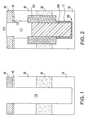
- FIG. 1shows a wafer for use in the invention, in which substrate 10 is a bulk silicon substrate, on which is formed a buffer layer 20 of SiGe alloy and a device layer 30 , also of SiGe.
- a layer of strained siliconwill be formed on the vertical face of the layer of SiGe.
- a transistor bodywill be formed within this vertical layer of strained silicon.
- Pad oxide 42 and pad nitride 45complete the structure.
- Layer 20is formed on the surface of substrate 10 to accommodate the difference in atomic spacing of the two materials. There will be dislocations and other material defects in layer 20 that would be detrimental to transistor operation.
- layer 30a fully relaxed SiGe layer, is formed to hold the transistors, not only in the cell illustrated, but also, optionally, in logic circuits containing planar transistors that are formed elsewhere in an integrated circuit that contains the DRAM cell illustrated.
- Aperture 110is a deep trench, e.g. 8 microns deep, that will contain a DRAM cell having a vertical field effect transistor (FET) for an access device, as is known in the art.
- FETvertical field effect transistor
- the inventionmay be used with a DRAM integrated circuit, or with a circuit having other functions that contains a DRAM array.
- a DRAM integrated circuitor with a circuit having other functions that contains a DRAM array.
- many composite systems that are fabricated in integrated circuit form,include memories that are formed from DRAMs.
- FIG. 2illustrates the same area after some intermediate steps that form a capacitor 100 .
- Capacitor 100has a dielectric 12 , e.g. oxide (SiO2) or a layer of oxide adjacent to a layer of nitride (Si3N4).
- a central electrode 105formed by deposition of doped polysilicon (poly) or other conducting materials such as metals, completes the capacitor and will make contact with an access transistor to be constructed in the upper part of the trench.
- a collar 107(illustratively oxide) has been formed after the completion of the initial portion of the capacitor and before the extension of the central electrode.
- Oxide collarsare conventional and are formed by oxidizing the vertical silicon (and/or the SiGe) exposed by the construction of the trench.
- the collarmay be formed on the trench sidewall by conventional deposition techniques such as chemical vapor deposition (CVD).
- CVDchemical vapor deposition
- the deposited materialis removed from the trench bottom by techniques such as reactive ion etching (RIE), leaving the collar material on the trench sidewall.
- RIEreactive ion etching
- Other insulating materialsmay also be used to form the collar.
- the central portion of the trenchis filled with a conducting material such as polysilicon, or a combination of several conducting materials such as polysilicon and titanium nitride, that is then recessed to leave a portion of the collar exposed.
- a conducting materialsuch as polysilicon, or a combination of several conducting materials such as polysilicon and titanium nitride, that is then recessed to leave a portion of the collar exposed.
- the collarextends below and above the defect-laden layer 20 , thus also protecting the other parts of the structure from being affected by defects in layer 20 .
- aperture 111now remains above the top surface of poly electrode 107 .
- the width of aperture 111 in this Figure, denoted by bracket 112will be referred to as the original trench width.
- bracket 112the width of aperture 111 in this Figure, denoted by bracket 112 .
- the process of forming the capacitor and the collarhas consumed some of the SiGe in the device layer 30 , leaving an overhang below the pad oxide 42 that is denoted by bracket 122 .
- This overhanghas presented a problem in the prior art because conventional deposition of materials such as the gate electrode will not completely fill the trench due to the overhang, so that voids tend to form in the filling material.
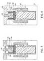
- FIG. 3shows the same cell after a step of etching the top and inner corners of collar 107 in a wet etch step to form apertures 113 extending transversely from and below the top surface of poly 105 .
- FIG. 4shows the result of filling apertures 113 in the poly and then recessing the fill material to leave the new poly only in the apertures 113 , forming buried straps 106 .
- FIG. 5shows the result of depositing a layer of insulator 132 , referred to as the trench top oxide that fills the space above the central electrode of the capacitor and isolates it from the gate electrode of the vertical transistor that will be deposited.
- an annealing stepdrives dopant from the poly 105 and/or from the deposited buried strap into the SiGe device layer to form an extended buried strap 106 ′ that extends the dopant into the device layer, making contact with an area that will be part of the lower electrode of a vertical FET.
- FIG. 6shows the result of an epitaxial deposition of silicon 134 , referred to as a body layer, which has been deposited epitaxially on the exposed surface of layer 30 .
- Layer 134will become part of the body of the vertical FET.
- Epi layer 134has been deposited to a nominal thickness equal to the length of overhang 122 , so that the new vertical surface of the transistor body is substantially aligned with the original trench width defined by the vertical face of pad nitride 45 .
- the silicon in layer 134is strained. That strain increases the mobility of the vertical transistor and therefore increases the performance of the transistor.
- the transverse dimension of the trenchis decreased by twice the thickness of layer 134 .
- the performance of a transistor in a strained silicon layeris greater than the performance of a comparable transistor in a SiGe layer. In some cases, the extra performance may not be required and it may be preferable to put down a layer of SiGe on the vertical face of the SiGe layer and to use that layer as the body of the vertical transistor.
- the transverse dimension of the trenchis decreased by twice the thickness of layer 134 .
- the dimension of the trench and the spacing between the gate electrode and the passing wordline(shown in FIG. 9 ) is fixed, so that decreasing the trench width frees up area for other purposes, as will be described below.
- FIG. 7shows the transistor area, denoted generally with numeral 150 and having the result of forming gate dielectric 152 e.g., thermally grown oxide, on layer 134 , filling the remaining aperture with conducting material 154 and then optionally etching the outer portion of the top of the conducting material 155 to form apertures 156 .
- the conducting material 154is preferred to be polysilicon.
- FIG. 8shows the result of stripping pad nitride 45 , implanting dopant in the upper portion of layer 30 to form, depending on the operation of the transistor, a drain or source 157 of the transistor and filling apertures 156 with array top insulating material 162 such as oxide 162 , separating the gate contact 155 from the drain 157 .
- Isolation trenchesmay be formed at any convenient time to isolate cells and devices in the other portion of the circuit.
- the cellis not complete until a contact has been formed to the bitline of the DRAM array (at the upper electrode of the vertical transistor) and a gate contact has been formed to the wordline of the DRAM array (at the gate of the access transistor).
- FIG. 9shows the result of an intermediate step of forming a wordline structure 175 or 177 , comprising an extension 172 of the gate contact 155 and associated cap and spacer layers.
- Polysilicon, tungsten, tungsten silicide, or any other suitable conducting materials, or any of their combinationmay be used to form the wordline structure.
- Layer 172 that is in contact with poly 155may be capped by an insulating material 176 , such as nitride.
- the wordline structuresare formed by deposition of a layer 172 of wordline material and a nitride cap.
- Gate contact lithographydefines a stack of conductive member 172 capped with nitride 176 .
- Sidewalls 174are formed on the sides of the gate stack by depositing a nitride layer or other suitable materials by a conventional process such as CVD and etching the flat portions in a directional etching process such as RIE.
- FIG. 9Three structures are shown in FIG. 9 —the wordline structure in the center, denoted by numeral 175 and two passing wordline structures 177 that are wordlines for rows of cells in front of and behind the cell illustrated, using a conventional folded wordline layout.
- the wordlinemay be offset from the center of element 155 .
- the spacing 183 between the gate contact for the illustrated cell and the passing wordline on the rightis set by the groundrules. For a given groundrule, therefore, the increase in trench width caused by the consumption of silicon reduced the space available for the bitline contact for the trench, which has to be outside the trench and not contacting the passing wordline 177 .
- FIG. 10Ashows the cell after depositing a first layer of interlevel dielectric 182 (BPSG in this case), opening a contact aperture for the bitline contact and filling the aperture with conducting materials such as W or polysilicon to form contact 185 .
- BPSGinterlevel dielectric
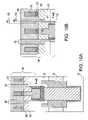
- the region of the top of the cell denoted with bracket 190is enlarged in FIG. 10B , showing section of array top dielectric 162 penetrated by gate electrode contact 155 in the center and two bitline contacts 185 on the left and right of gate contact 155 .
- a bracket labeled 185indicates the width of the bitline contact according to the invention.
- Arrow 186indicates the width in a prior art arrangement in which the layer 134 of strained silicon is not deposited, so that the distance 186 is the width available for the bitline contact—extending from the recessed trench wall on the right to the left edge of arrow 185 , which is at the location of the vertical edge of pad nitride 45 .
- the distance between the trench walls as they were recessed into the layer 30set the width of the trench and therefore by subtraction the width available for the bitline contact.
- the added width of the strained silicon 134narrows the trench aperture and therefore increases the space available for the bitline contact. With a wider contact, the resistance of the electron path in and out of the capacitor is reduced.
- bitline contact 185is in electrical contact with the top of layer 134 and with drain or source 157 .
Landscapes
- Engineering & Computer Science (AREA)
- Manufacturing & Machinery (AREA)
- Semiconductor Memories (AREA)
- Insulated Gate Type Field-Effect Transistor (AREA)
Abstract
Description
The field of the invention is that of integrated circuit processing, in particular DRAM cells having vertical pass transistors.
In the fabrication of vertical-transistor DRAM cells, both in DRAMs and in DRAM arrays in ASICs and other complex systems, the formation of the capacitor removes silicon from the trench walls in the upper part of the trench, producing an overhang of the pad nitride.
That overhang interferes with filling the upper part of the trench with the gate electrode, leaving voids in the gate electrode that are disadvantageous.
Further, for a given ground rule and inter-cell spacing, the space for bitline contacts to the upper electrode of the vertical transistor is limited. The removal of silicon from the upper trench walls further reduces the width of the bitline contacts, extending outward from the trench walls into the silicon well.
Expanding the width of the cell to accommodate a wider trench and a wider bitline contact is not an option, given the overwhelming need to reduce the transverse dimensions of the cells.
As the demand for higher performance devices increases steadily, one attractive option is the use of strained silicon to improve electron mobility.
A feature of the invention is compensation for the overhang of the pad nitride in a trench capacitor vertical-transistor DRAM cell by forming an epitaxial strained silicon layer on the trench walls that improves transistor mobility.
Another feature of the invention is that the added silicon removes voids from the poly trench fill.
Yet another feature of the invention is that the extra width of the added silicon reduces resistance on the bitline contact.
Yet another feature of the invention is that forming a vertical strained silicon channel improves the performance of the vertical device.
Aperture110 is a deep trench, e.g. 8 microns deep, that will contain a DRAM cell having a vertical field effect transistor (FET) for an access device, as is known in the art.
The invention may be used with a DRAM integrated circuit, or with a circuit having other functions that contains a DRAM array. In contemporary practice, many composite systems that are fabricated in integrated circuit form, include memories that are formed from DRAMs.
A collar107 (illustratively oxide) has been formed after the completion of the initial portion of the capacitor and before the extension of the central electrode. Oxide collars are conventional and are formed by oxidizing the vertical silicon (and/or the SiGe) exposed by the construction of the trench. Alternatively, the collar may be formed on the trench sidewall by conventional deposition techniques such as chemical vapor deposition (CVD). The deposited material is removed from the trench bottom by techniques such as reactive ion etching (RIE), leaving the collar material on the trench sidewall. Other insulating materials may also be used to form the collar.
After the collar has been formed, the central portion of the trench is filled with a conducting material such as polysilicon, or a combination of several conducting materials such as polysilicon and titanium nitride, that is then recessed to leave a portion of the collar exposed.
In this case, the collar extends below and above the defect-laden layer 20, thus also protecting the other parts of the structure from being affected by defects inlayer 20.
Anaperture 111 now remains above the top surface ofpoly electrode 107. The width ofaperture 111 in this Figure, denoted bybracket 112, will be referred to as the original trench width. As can be seen inFIG. 2 , the process of forming the capacitor and the collar has consumed some of the SiGe in thedevice layer 30, leaving an overhang below thepad oxide 42 that is denoted bybracket 122. This overhang has presented a problem in the prior art because conventional deposition of materials such as the gate electrode will not completely fill the trench due to the overhang, so that voids tend to form in the filling material.
At any convenient time, an annealing step drives dopant from thepoly 105 and/or from the deposited buried strap into the SiGe device layer to form an extended buriedstrap 106′ that extends the dopant into the device layer, making contact with an area that will be part of the lower electrode of a vertical FET.
The process of depositing oxide in the aperture and etching any material that has adhered to the trench walls will increase the extent ofoverhang 122.
Since the inter-atomic distance in SiGe is greater than the corresponding distance in crystalline silicon, the silicon inlayer 134 is strained. That strain increases the mobility of the vertical transistor and therefore increases the performance of the transistor.
The transverse dimension of the trench is decreased by twice the thickness oflayer 134. The performance of a transistor in a strained silicon layer is greater than the performance of a comparable transistor in a SiGe layer. In some cases, the extra performance may not be required and it may be preferable to put down a layer of SiGe on the vertical face of the SiGe layer and to use that layer as the body of the vertical transistor.
The transverse dimension of the trench is decreased by twice the thickness oflayer 134. For a given ground rule, the dimension of the trench and the spacing between the gate electrode and the passing wordline (shown inFIG. 9 ) is fixed, so that decreasing the trench width frees up area for other purposes, as will be described below.
The cell is not complete until a contact has been formed to the bitline of the DRAM array (at the upper electrode of the vertical transistor) and a gate contact has been formed to the wordline of the DRAM array (at the gate of the access transistor).
The wordline structures are formed by deposition of alayer 172 of wordline material and a nitride cap. Gate contact lithography defines a stack ofconductive member 172 capped withnitride 176.
Three structures are shown in FIG.9—the wordline structure in the center, denoted bynumeral 175 and two passing wordlinestructures 177 that are wordlines for rows of cells in front of and behind the cell illustrated, using a conventional folded wordline layout. Alternatively (not shown), the wordline may be offset from the center ofelement 155.
The spacing183 between the gate contact for the illustrated cell and the passing wordline on the right is set by the groundrules. For a given groundrule, therefore, the increase in trench width caused by the consumption of silicon reduced the space available for the bitline contact for the trench, which has to be outside the trench and not contacting the passingwordline 177.
The region of the top of the cell denoted withbracket 190 is enlarged inFIG. 10B , showing section of array top dielectric162 penetrated bygate electrode contact 155 in the center and twobitline contacts 185 on the left and right ofgate contact 155.
Above the right bitline contact185 a bracket labeled185 indicates the width of the bitline contact according to the invention.Arrow 186 indicates the width in a prior art arrangement in which thelayer 134 of strained silicon is not deposited, so that thedistance 186 is the width available for the bitline contact—extending from the recessed trench wall on the right to the left edge ofarrow 185, which is at the location of the vertical edge ofpad nitride 45.
In the past, the distance between the trench walls as they were recessed into thelayer 30 set the width of the trench and therefore by subtraction the width available for the bitline contact.
In a cell according to the invention, the added width of thestrained silicon 134 narrows the trench aperture and therefore increases the space available for the bitline contact. With a wider contact, the resistance of the electron path in and out of the capacitor is reduced.
The bottom ofbitline contact 185 is in electrical contact with the top oflayer 134 and with drain orsource 157.
While the invention has been described in terms of a single preferred embodiment, those skilled in the art will recognize that the invention can be practiced in various versions within the spirit and scope of the following claims.
Claims (14)
1. An integrated circuit structure comprising a vertical transistor comprising:
a semiconductor wafer having a layer of SiGe alloy above and substantially parallel to a bulk semiconductor substrate;
said wafer having a trench etched through the layer of SiGe into the bulk substrate;
an isolating collar formed within the trench;
a lower contact for the vertical transistor formed above the isolating collar, the lower contact being in contact with a portion of the SiGe layer above the isolating collar;
a vertical body layer of strained silicon formed on an exposed vertical surface of the SiGe layer within the trench, said exposed vertical surface being recessed transversely from an original trench width, and said body layer extending upward substantially at said original trench width from the top surface of the lower contact, whereby the body layer of silicon is strained;
a gate dielectric layer formed on an exposed vertical surface of the silicon body layer within the trench, thereby isolating the body layer from the trench interior;
a gate electrode formed within the trench and separated from the body layer of silicon by the gate dielectric layer; and
an upper electrode of the transistor formed in contact with the body layer of silicon, thereby establishing a path for conducting carriers from said lower contact to said upper contact through said vertical body layer.
2. A structure according toclaim 1 , in which said SiGe layer is a fully relaxed layer separated from a silicon bulk substrate by a buffer layer of SiGe.
3. A structure according toclaim 1 , in which said body layer of silicon is formed under an overhang of a pad dielectric and extending out into said trench to said original trench width;
further comprising a portion of said gate electrode extending up to a wafer surface thereby leaving a central gate electrode of width less than said original trench width, said central gate electrode having at least one aperture adjacent thereto that extends outward to said original trench width and down to make contact with said upper electrode; and
dielectric filling said aperture adjacent to said central gate electrode to isolate said central gate electrode.
4. A structure according toclaim 3 , further comprising a gate contact formed on said central gate electrode, capped by a gate contact cap and bracketed by gate contact sidewalls; and
an aperture for a drain contact formed adjacent to one of said gate contact sidewalls, said aperture being located transversely with respect to said central gate electrode to make contact with said vertical body layer and with said drain.
5. A structure according toclaim 2 , in which said body layer of silicon is formed under an overhang of a pad dielectric and extending out into said trench to said original trench width;
further comprising a portion of said gate electrode extending up to a wafer surface thereby leaving a central gate electrode of width less than said original trench width, said central gate electrode having at least one aperture adjacent thereto that extends outward to said original trench width and down to make contact with said upper electrode; and
dielectric filling said aperture adjacent to said central gate electrode to isolate said central gate electrode.
6. A structure according toclaim 5 , further comprising a gate contact formed on said central gate electrode, capped by a gate contact cap and bracketed by gate contact sidewalls; and
an aperture for a drain contact formed adjacent to one of said gate contact sidewalls, said aperture being located transversely with respect to said central gate electrode to make contact with said vertical body layer and with said drain.
7. An integrated circuit containing at least one DRAM cell having a vertical transistor comprising:
a wafer having a layer of SiGe alloy above a bulk semiconductor substrate;
a trench having an original trench width extending down through the layer of SiGe into the bulk substrate;
a capacitor formed within a lower portion of said trench;
an isolating collar formed within said trench above said capacitor;
a lower contact for the vertical transistor formed above said isolating collar, said lower contact being in contact with a portion of the SiGe layer above the isolating collar;
an isolating layer formed within the trench overlapping vertically the lower contact, thereby separating said capacitor from an upper portion of said trench;
a vertical body layer of strained silicon disposed on an exposed vertical surface of said SiGe layer within the trench, said exposed vertical surface being recessed transversely from an original trench width, and extending upward substantially at said original trench width from the top surface of the isolating layer, whereby said body layer of silicon is strained;
a gate dielectric formed on an exposed vertical surface of said silicon body layer within the trench, thereby isolating said silicon body layer from the trench interior;
a gate electrode formed within the trench and separated from said body layer of silicon by said gate dielectric layer; and
an upper electrode of a FET transistor in contact with said body layer of silicon, thereby establishing a path for electrons from said lower contact to said upper contact through said vertical body layer.
8. A structure according toclaim 7 , in which said SiGe layer is a fully relaxed layer separated from a silicon bulk substrate by a buffer layer of SiGe.
9. A circuit according toclaim 7 , in which said body layer of silicon is formed under an overhang of a pad dielectric and extending out into said trench to said original trench width;
further comprising a portion of said gate electrode extending up to a wafer surface thereby leaving a central gate electrode of width less than said original trench width, said central gate electrode having at least one aperture adjacent thereto that extends outward to said original trench width and down to make contact with said upper electrode; and
dielectric filling said aperture adjacent to said central gate electrode to isolate said central gate electrode.
10. A circuit according toclaim 9 , further comprising a gate contact formed on said central gate electrode, capped by a gate contact cap and bracketed by gate contact sidewalls; and
an aperture for a drain contact fanned adjacent to one of said gate contact sidewalls, said aperture being located transversely with respect to said central gate electrode to make contact with said vertical body layer and with said drain.
11. A circuit according toclaim 8 , in which said body layer of silicon is formed under an overhang of a pad dielectric and extending out into said trench to said original trench width;
further comprising a portion of said gate electrode extending up to a wafer surface thereby leaving a central gate electrode of width less than said original trench width, said central gate electrode having at least one aperture adjacent thereto that extends outward to said original trench width and down to make contact with said upper electrode; and
dielectric tilling said aperture adjacent to said central gate electrode to isolate said central gate electrode.
12. A circuit according toclaim 11 , further comprising a gate contact formed on said central gate electrode, capped by a gate contact cap and bracketed by gate contact sidewalls; and
an aperture for a drain contact formed adjacent to one of said gate contact sidewalk, said aperture being located transversely with respect to said central gate electrode to make contact with said vertical body layer and with said drain.
13. A circuit according toclaim 7 , in which said at least one DRAM cell comprises an array of DRAM cells.
14. A circuit according toclaim 13 , in which said circuit comprises a dynamic random access memory having an array of DRAM cells.
Priority Applications (2)
| Application Number | Priority Date | Filing Date | Title |
|---|---|---|---|
| US10/605,227US7170126B2 (en) | 2003-09-16 | 2003-09-16 | Structure of vertical strained silicon devices |
| JP2004266297AJP4160942B2 (en) | 2003-09-16 | 2004-09-14 | Method for forming vertical transistor, method for forming DRAM with vertical transistor, integrated circuit structure with vertical transistor, and integrated circuit including at least one DRAM cell with vertical transistor |
Applications Claiming Priority (1)
| Application Number | Priority Date | Filing Date | Title |
|---|---|---|---|
| US10/605,227US7170126B2 (en) | 2003-09-16 | 2003-09-16 | Structure of vertical strained silicon devices |
Publications (2)
| Publication Number | Publication Date |
|---|---|
| US20050059214A1 US20050059214A1 (en) | 2005-03-17 |
| US7170126B2true US7170126B2 (en) | 2007-01-30 |
Family
ID=34273185
Family Applications (1)
| Application Number | Title | Priority Date | Filing Date |
|---|---|---|---|
| US10/605,227Expired - Fee RelatedUS7170126B2 (en) | 2003-09-16 | 2003-09-16 | Structure of vertical strained silicon devices |
Country Status (2)
| Country | Link |
|---|---|
| US (1) | US7170126B2 (en) |
| JP (1) | JP4160942B2 (en) |
Cited By (8)
| Publication number | Priority date | Publication date | Assignee | Title |
|---|---|---|---|---|
| US20080169494A1 (en)* | 2006-04-04 | 2008-07-17 | Kangguo Cheng | Self-aligned body contact for a semiconductor-on-insulator trench device and method of fabricating same |
| US20090184356A1 (en)* | 2008-01-18 | 2009-07-23 | International Business Machines Corporation | Deep trench capacitor in a soi substrate having a laterally protruding buried strap |
| US20100207245A1 (en)* | 2009-02-13 | 2010-08-19 | International Business Machines Corporation | Highly scalable trench capacitor |
| US9871055B1 (en) | 2016-08-05 | 2018-01-16 | Samsung Electronics Co., Ltd. | Vertical-type memory device |
| US10395982B2 (en) | 2017-07-07 | 2019-08-27 | Samsung Electronics Co., Ltd. | Three-dimensional semiconductor device and method of fabricating the same |
| US10395988B1 (en) | 2018-04-10 | 2019-08-27 | International Business Machines Corporation | Vertical FET transistor with reduced source/drain contact resistance |
| US10916582B2 (en)* | 2017-12-30 | 2021-02-09 | Spin Memory, Inc. | Vertically-strained silicon device for use with a perpendicular magnetic tunnel junction (PMTJ) |
| US12382672B2 (en) | 2021-11-09 | 2025-08-05 | Samsung Electronics Co., Ltd. | Epitaxial wafer and semiconductor memory device using the same |
Families Citing this family (40)
| Publication number | Priority date | Publication date | Assignee | Title |
|---|---|---|---|---|
| WO2003017336A2 (en)* | 2001-08-13 | 2003-02-27 | Amberwave Systems Corporation | Dram trench capacitor and method of making the same |
| US7456476B2 (en) | 2003-06-27 | 2008-11-25 | Intel Corporation | Nonplanar semiconductor device with partially or fully wrapped around gate electrode and methods of fabrication |
| US6909151B2 (en) | 2003-06-27 | 2005-06-21 | Intel Corporation | Nonplanar device with stress incorporation layer and method of fabrication |
| US7268058B2 (en)* | 2004-01-16 | 2007-09-11 | Intel Corporation | Tri-gate transistors and methods to fabricate same |
| US7154118B2 (en)* | 2004-03-31 | 2006-12-26 | Intel Corporation | Bulk non-planar transistor having strained enhanced mobility and methods of fabrication |
| US20050285175A1 (en)* | 2004-06-23 | 2005-12-29 | International Business Machines Corporation | Vertical SOI Device |
| US7042009B2 (en) | 2004-06-30 | 2006-05-09 | Intel Corporation | High mobility tri-gate devices and methods of fabrication |
| US7348284B2 (en) | 2004-08-10 | 2008-03-25 | Intel Corporation | Non-planar pMOS structure with a strained channel region and an integrated strained CMOS flow |
| US7422946B2 (en)* | 2004-09-29 | 2008-09-09 | Intel Corporation | Independently accessed double-gate and tri-gate transistors in same process flow |
| US7332439B2 (en)* | 2004-09-29 | 2008-02-19 | Intel Corporation | Metal gate transistors with epitaxial source and drain regions |
| US7361958B2 (en)* | 2004-09-30 | 2008-04-22 | Intel Corporation | Nonplanar transistors with metal gate electrodes |
| US20060086977A1 (en) | 2004-10-25 | 2006-04-27 | Uday Shah | Nonplanar device with thinned lower body portion and method of fabrication |
| US7518196B2 (en) | 2005-02-23 | 2009-04-14 | Intel Corporation | Field effect transistor with narrow bandgap source and drain regions and method of fabrication |
| US20060202266A1 (en)* | 2005-03-14 | 2006-09-14 | Marko Radosavljevic | Field effect transistor with metal source/drain regions |
| US7858481B2 (en) | 2005-06-15 | 2010-12-28 | Intel Corporation | Method for fabricating transistor with thinned channel |
| US7547637B2 (en) | 2005-06-21 | 2009-06-16 | Intel Corporation | Methods for patterning a semiconductor film |
| US7279375B2 (en)* | 2005-06-30 | 2007-10-09 | Intel Corporation | Block contact architectures for nanoscale channel transistors |
| US7402875B2 (en)* | 2005-08-17 | 2008-07-22 | Intel Corporation | Lateral undercut of metal gate in SOI device |
| US20070090416A1 (en)* | 2005-09-28 | 2007-04-26 | Doyle Brian S | CMOS devices with a single work function gate electrode and method of fabrication |
| US7479421B2 (en)* | 2005-09-28 | 2009-01-20 | Intel Corporation | Process for integrating planar and non-planar CMOS transistors on a bulk substrate and article made thereby |
| US20070090408A1 (en)* | 2005-09-29 | 2007-04-26 | Amlan Majumdar | Narrow-body multiple-gate FET with dominant body transistor for high performance |
| US7485503B2 (en) | 2005-11-30 | 2009-02-03 | Intel Corporation | Dielectric interface for group III-V semiconductor device |
| US20070152266A1 (en)* | 2005-12-29 | 2007-07-05 | Intel Corporation | Method and structure for reducing the external resistance of a three-dimensional transistor through use of epitaxial layers |
| US7473593B2 (en)* | 2006-01-11 | 2009-01-06 | International Business Machines Corporation | Semiconductor transistors with expanded top portions of gates |
| US7795661B2 (en)* | 2006-03-07 | 2010-09-14 | International Business Machines Corporation | Vertical SOI transistor memory cell |
| US8143646B2 (en) | 2006-08-02 | 2012-03-27 | Intel Corporation | Stacking fault and twin blocking barrier for integrating III-V on Si |
| US7563670B2 (en)* | 2006-11-13 | 2009-07-21 | International Business Machines Corporation | Method for etching single-crystal semiconductor selective to amorphous/polycrystalline semiconductor and structure formed by same |
| US20080157225A1 (en)* | 2006-12-29 | 2008-07-03 | Suman Datta | SRAM and logic transistors with variable height multi-gate transistor architecture |
| TW200913159A (en)* | 2007-09-12 | 2009-03-16 | Nanya Technology Corp | Semiconductor devices and fabrication methods thereof |
| KR101320518B1 (en)* | 2007-10-24 | 2013-12-19 | 삼성전자주식회사 | Integrated circuit semiconductor device having stacked level transistors portion and fabrication method thereof |
| ES2489615T3 (en)* | 2007-12-11 | 2014-09-02 | Apoteknos Para La Piel, S.L. | Use of a compound derived from p-hydroxyphenyl propionic acid for the treatment of psoriasis |
| US8362566B2 (en) | 2008-06-23 | 2013-01-29 | Intel Corporation | Stress in trigate devices using complimentary gate fill materials |
| TWI478341B (en)* | 2011-10-31 | 2015-03-21 | 茂達電子股份有限公司 | Power transistor device and manufacturing method thereof |
| TWI462295B (en)* | 2011-11-15 | 2014-11-21 | Anpec Electronics Corp | Ditch type power transistor component and manufacturing method thereof |
| KR102512718B1 (en)* | 2016-03-17 | 2023-03-23 | 삼성디스플레이 주식회사 | Thin film transistor substrate, organic light emitting display using the same, method for manufacturing thin film transistor substrate |
| KR102620596B1 (en) | 2016-08-22 | 2024-01-04 | 삼성전자주식회사 | Semiconductor device |
| US9647112B1 (en)* | 2016-09-22 | 2017-05-09 | International Business Machines Corporation | Fabrication of strained vertical P-type field effect transistors by bottom condensation |
| KR102395987B1 (en)* | 2017-04-05 | 2022-05-10 | 삼성전자주식회사 | Vertical stack memory device |
| US11164816B2 (en)* | 2019-09-05 | 2021-11-02 | Nanya Technology Corporation | Semiconductor device and method for fabricating the same |
| CN114256153B (en)* | 2020-09-23 | 2024-06-07 | 长鑫存储技术有限公司 | Semiconductor structure forming method and semiconductor structure |
Citations (80)
| Publication number | Priority date | Publication date | Assignee | Title |
|---|---|---|---|---|
| US3602841A (en) | 1970-06-18 | 1971-08-31 | Ibm | High frequency bulk semiconductor amplifiers and oscillators |
| US4665415A (en) | 1985-04-24 | 1987-05-12 | International Business Machines Corporation | Semiconductor device with hole conduction via strained lattice |
| US4853076A (en) | 1983-12-29 | 1989-08-01 | Massachusetts Institute Of Technology | Semiconductor thin films |
| US4855245A (en) | 1985-09-13 | 1989-08-08 | Siemens Aktiengesellschaft | Method of manufacturing integrated circuit containing bipolar and complementary MOS transistors on a common substrate |
| US4952524A (en) | 1989-05-05 | 1990-08-28 | At&T Bell Laboratories | Semiconductor device manufacture including trench formation |
| US4958213A (en) | 1987-12-07 | 1990-09-18 | Texas Instruments Incorporated | Method for forming a transistor base region under thick oxide |
| US5006913A (en) | 1988-11-05 | 1991-04-09 | Mitsubishi Denki Kabushiki Kaisha | Stacked type semiconductor device |
| US5060030A (en) | 1990-07-18 | 1991-10-22 | Raytheon Company | Pseudomorphic HEMT having strained compensation layer |
| US5081513A (en) | 1991-02-28 | 1992-01-14 | Xerox Corporation | Electronic device with recovery layer proximate to active layer |
| US5108843A (en) | 1988-11-30 | 1992-04-28 | Ricoh Company, Ltd. | Thin film semiconductor and process for producing the same |
| US5134085A (en) | 1991-11-21 | 1992-07-28 | Micron Technology, Inc. | Reduced-mask, split-polysilicon CMOS process, incorporating stacked-capacitor cells, for fabricating multi-megabit dynamic random access memories |
| US5256550A (en) | 1988-11-29 | 1993-10-26 | Hewlett-Packard Company | Fabricating a semiconductor device with strained Si1-x Gex layer |
| US5310446A (en) | 1990-01-10 | 1994-05-10 | Ricoh Company, Ltd. | Method for producing semiconductor film |
| US5354695A (en) | 1992-04-08 | 1994-10-11 | Leedy Glenn J | Membrane dielectric isolation IC fabrication |
| US5371399A (en) | 1991-06-14 | 1994-12-06 | International Business Machines Corporation | Compound semiconductor having metallic inclusions and devices fabricated therefrom |
| US5391510A (en) | 1992-02-28 | 1995-02-21 | International Business Machines Corporation | Formation of self-aligned metal gate FETs using a benignant removable gate material during high temperature steps |
| US5459346A (en) | 1988-06-28 | 1995-10-17 | Ricoh Co., Ltd. | Semiconductor substrate with electrical contact in groove |
| US5461243A (en) | 1993-10-29 | 1995-10-24 | International Business Machines Corporation | Substrate for tensilely strained semiconductor |
| US5557122A (en) | 1995-05-12 | 1996-09-17 | Alliance Semiconductors Corporation | Semiconductor electrode having improved grain structure and oxide growth properties |
| US5561302A (en) | 1994-09-26 | 1996-10-01 | Motorola, Inc. | Enhanced mobility MOSFET device and method |
| US5670798A (en) | 1995-03-29 | 1997-09-23 | North Carolina State University | Integrated heterostructures of Group III-V nitride semiconductor materials including epitaxial ohmic contact non-nitride buffer layer and methods of fabricating same |
| US5679965A (en) | 1995-03-29 | 1997-10-21 | North Carolina State University | Integrated heterostructures of Group III-V nitride semiconductor materials including epitaxial ohmic contact, non-nitride buffer layer and methods of fabricating same |
| US5847419A (en)* | 1996-09-17 | 1998-12-08 | Kabushiki Kaisha Toshiba | Si-SiGe semiconductor device and method of fabricating the same |
| US5861651A (en) | 1997-02-28 | 1999-01-19 | Lucent Technologies Inc. | Field effect devices and capacitors with improved thin film dielectrics and method for making same |
| US5880040A (en) | 1996-04-15 | 1999-03-09 | Macronix International Co., Ltd. | Gate dielectric based on oxynitride grown in N2 O and annealed in NO |
| US5940736A (en) | 1997-03-11 | 1999-08-17 | Lucent Technologies Inc. | Method for forming a high quality ultrathin gate oxide layer |
| US5940716A (en) | 1996-03-15 | 1999-08-17 | Samsung Electronics Co., Ltd. | Methods of forming trench isolation regions using repatterned trench masks |
| US5960297A (en) | 1997-07-02 | 1999-09-28 | Kabushiki Kaisha Toshiba | Shallow trench isolation structure and method of forming the same |
| US5989978A (en) | 1998-07-16 | 1999-11-23 | Chartered Semiconductor Manufacturing, Ltd. | Shallow trench isolation of MOSFETS with reduced corner parasitic currents |
| US6008126A (en) | 1992-04-08 | 1999-12-28 | Elm Technology Corporation | Membrane dielectric isolation IC fabrication |
| US6025280A (en) | 1997-04-28 | 2000-02-15 | Lucent Technologies Inc. | Use of SiD4 for deposition of ultra thin and controllable oxides |
| US6066545A (en) | 1997-12-09 | 2000-05-23 | Texas Instruments Incorporated | Birdsbeak encroachment using combination of wet and dry etch for isolation nitride |
| US6090684A (en) | 1998-07-31 | 2000-07-18 | Hitachi, Ltd. | Method for manufacturing semiconductor device |
| US6107143A (en) | 1998-03-02 | 2000-08-22 | Samsung Electronics Co., Ltd. | Method for forming a trench isolation structure in an integrated circuit |
| US6117722A (en) | 1999-02-18 | 2000-09-12 | Taiwan Semiconductor Manufacturing Company | SRAM layout for relaxing mechanical stress in shallow trench isolation technology and method of manufacture thereof |
| US6133071A (en) | 1997-10-15 | 2000-10-17 | Nec Corporation | Semiconductor device with plate heat sink free from cracks due to thermal stress and process for assembling it with package |
| US6165383A (en) | 1998-04-10 | 2000-12-26 | Organic Display Technology | Useful precursors for organic electroluminescent materials and devices made from such materials |
| US6221735B1 (en) | 2000-02-15 | 2001-04-24 | Philips Semiconductors, Inc. | Method for eliminating stress induced dislocations in CMOS devices |
| US6228694B1 (en) | 1999-06-28 | 2001-05-08 | Intel Corporation | Method of increasing the mobility of MOS transistors by use of localized stress regions |
| US6255169B1 (en) | 1999-02-22 | 2001-07-03 | Advanced Micro Devices, Inc. | Process for fabricating a high-endurance non-volatile memory device |
| US6261964B1 (en) | 1997-03-14 | 2001-07-17 | Micron Technology, Inc. | Material removal method for forming a structure |
| US6265317B1 (en) | 2001-01-09 | 2001-07-24 | Taiwan Semiconductor Manufacturing Company | Top corner rounding for shallow trench isolation |
| US20010009784A1 (en) | 1998-01-09 | 2001-07-26 | Yanjun Ma | Structure and method of making a sub-micron MOS transistor |
| US6274444B1 (en) | 1999-07-30 | 2001-08-14 | United Microelectronics Corp. | Method for forming mosfet |
| US6281532B1 (en) | 1999-06-28 | 2001-08-28 | Intel Corporation | Technique to obtain increased channel mobilities in NMOS transistors by gate electrode engineering |
| US6284626B1 (en) | 1999-04-06 | 2001-09-04 | Vantis Corporation | Angled nitrogen ion implantation for minimizing mechanical stress on side walls of an isolation trench |
| US6284623B1 (en) | 1999-10-25 | 2001-09-04 | Peng-Fei Zhang | Method of fabricating semiconductor devices using shallow trench isolation with reduced narrow channel effect |
| US6313486B1 (en) | 2000-06-15 | 2001-11-06 | Board Of Regents, The University Of Texas System | Floating gate transistor having buried strained silicon germanium channel layer |
| US6319794B1 (en) | 1998-10-14 | 2001-11-20 | International Business Machines Corporation | Structure and method for producing low leakage isolation devices |
| US6335239B1 (en)* | 1998-12-04 | 2002-01-01 | International Business Machines Corporation | Manufacturing a DRAM cell having an annular signal transfer region |
| US6362082B1 (en) | 1999-06-28 | 2002-03-26 | Intel Corporation | Methodology for control of short channel effects in MOS transistors |
| US6361885B1 (en) | 1998-04-10 | 2002-03-26 | Organic Display Technology | Organic electroluminescent materials and device made from such materials |
| US6368931B1 (en) | 2000-03-27 | 2002-04-09 | Intel Corporation | Thin tensile layers in shallow trench isolation and method of making same |
| US20020063292A1 (en) | 2000-11-29 | 2002-05-30 | Mark Armstrong | CMOS fabrication process utilizing special transistor orientation |
| US6403975B1 (en) | 1996-04-09 | 2002-06-11 | Max-Planck Gesellschaft Zur Forderung Der Wissenschafteneev | Semiconductor components, in particular photodetectors, light emitting diodes, optical modulators and waveguides with multilayer structures grown on silicon substrates |
| US6403486B1 (en) | 2001-04-30 | 2002-06-11 | Taiwan Semiconductor Manufacturing Company | Method for forming a shallow trench isolation |
| US6406973B1 (en) | 1999-06-29 | 2002-06-18 | Hyundai Electronics Industries Co., Ltd. | Transistor in a semiconductor device and method of manufacturing the same |
| US20020086472A1 (en) | 2000-12-29 | 2002-07-04 | Brian Roberds | Technique to obtain high mobility channels in MOS transistors by forming a strain layer on an underside of a channel |
| US20020086497A1 (en) | 2000-12-30 | 2002-07-04 | Kwok Siang Ping | Beaker shape trench with nitride pull-back for STI |
| US20020090791A1 (en) | 1999-06-28 | 2002-07-11 | Brian S. Doyle | Method for reduced capacitance interconnect system using gaseous implants into the ild |
| US6429061B1 (en) | 2000-07-26 | 2002-08-06 | International Business Machines Corporation | Method to fabricate a strained Si CMOS structure using selective epitaxial deposition of Si after device isolation formation |
| US6461936B1 (en) | 2002-01-04 | 2002-10-08 | Infineon Technologies Ag | Double pullback method of filling an isolation trench |
| US6476462B2 (en) | 1999-12-28 | 2002-11-05 | Texas Instruments Incorporated | MOS-type semiconductor device and method for making same |
| US6483171B1 (en) | 1999-08-13 | 2002-11-19 | Micron Technology, Inc. | Vertical sub-micron CMOS transistors on (110), (111), (311), (511), and higher order surfaces of bulk, SOI and thin film structures and method of forming same |
| US6493497B1 (en) | 2000-09-26 | 2002-12-10 | Motorola, Inc. | Electro-optic structure and process for fabricating same |
| US6498358B1 (en) | 2001-07-20 | 2002-12-24 | Motorola, Inc. | Structure and method for fabricating an electro-optic system having an electrochromic diffraction grating |
| US6501121B1 (en) | 2000-11-15 | 2002-12-31 | Motorola, Inc. | Semiconductor structure |
| US6503833B1 (en) | 2000-11-15 | 2003-01-07 | International Business Machines Corporation | Self-aligned silicide (salicide) process for strained silicon MOSFET ON SiGe and structure formed thereby |
| US6506652B2 (en) | 1998-11-13 | 2003-01-14 | Intel Corporation | Method of recessing spacers to improved salicide resistance on polysilicon gates |
| US20030032261A1 (en) | 2001-08-08 | 2003-02-13 | Ling-Yen Yeh | Method of preventing threshold voltage of MOS transistor from being decreased by shallow trench isolation formation |
| US6524935B1 (en) | 2000-09-29 | 2003-02-25 | International Business Machines Corporation | Preparation of strained Si/SiGe on insulator by hydrogen induced layer transfer technique |
| US20030040158A1 (en) | 2001-08-21 | 2003-02-27 | Nec Corporation | Semiconductor device and method of fabricating the same |
| US6531740B2 (en) | 2001-07-17 | 2003-03-11 | Motorola, Inc. | Integrated impedance matching and stability network |
| US6531369B1 (en) | 2000-03-01 | 2003-03-11 | Applied Micro Circuits Corporation | Heterojunction bipolar transistor (HBT) fabrication using a selectively deposited silicon germanium (SiGe) |
| US20030057184A1 (en) | 2001-09-22 | 2003-03-27 | Shiuh-Sheng Yu | Method for pull back SiN to increase rounding effect in a shallow trench isolation process |
| US20030067035A1 (en) | 2001-09-28 | 2003-04-10 | Helmut Tews | Gate processing method with reduced gate oxide corner and edge thinning |
| US6586300B1 (en)* | 2002-04-18 | 2003-07-01 | Infineon Technologies Ag | Spacer assisted trench top isolation for vertical DRAM's |
| US6621392B1 (en) | 2002-04-25 | 2003-09-16 | International Business Machines Corporation | Micro electromechanical switch having self-aligned spacers |
| US6635506B2 (en) | 2001-11-07 | 2003-10-21 | International Business Machines Corporation | Method of fabricating micro-electromechanical switches on CMOS compatible substrates |
| US6660582B2 (en)* | 2001-10-12 | 2003-12-09 | Infineon Technologies Ag | Method of forming a vertical field-effect transistor device |
- 2003
- 2003-09-16USUS10/605,227patent/US7170126B2/ennot_activeExpired - Fee Related
- 2004
- 2004-09-14JPJP2004266297Apatent/JP4160942B2/ennot_activeExpired - Fee Related
Patent Citations (93)
| Publication number | Priority date | Publication date | Assignee | Title |
|---|---|---|---|---|
| US3602841A (en) | 1970-06-18 | 1971-08-31 | Ibm | High frequency bulk semiconductor amplifiers and oscillators |
| US4853076A (en) | 1983-12-29 | 1989-08-01 | Massachusetts Institute Of Technology | Semiconductor thin films |
| US4665415A (en) | 1985-04-24 | 1987-05-12 | International Business Machines Corporation | Semiconductor device with hole conduction via strained lattice |
| US4855245A (en) | 1985-09-13 | 1989-08-08 | Siemens Aktiengesellschaft | Method of manufacturing integrated circuit containing bipolar and complementary MOS transistors on a common substrate |
| US4958213A (en) | 1987-12-07 | 1990-09-18 | Texas Instruments Incorporated | Method for forming a transistor base region under thick oxide |
| US5565697A (en) | 1988-06-28 | 1996-10-15 | Ricoh Company, Ltd. | Semiconductor structure having island forming grooves |
| US5459346A (en) | 1988-06-28 | 1995-10-17 | Ricoh Co., Ltd. | Semiconductor substrate with electrical contact in groove |
| US5006913A (en) | 1988-11-05 | 1991-04-09 | Mitsubishi Denki Kabushiki Kaisha | Stacked type semiconductor device |
| US5256550A (en) | 1988-11-29 | 1993-10-26 | Hewlett-Packard Company | Fabricating a semiconductor device with strained Si1-x Gex layer |
| US5108843A (en) | 1988-11-30 | 1992-04-28 | Ricoh Company, Ltd. | Thin film semiconductor and process for producing the same |
| US4952524A (en) | 1989-05-05 | 1990-08-28 | At&T Bell Laboratories | Semiconductor device manufacture including trench formation |
| US5310446A (en) | 1990-01-10 | 1994-05-10 | Ricoh Company, Ltd. | Method for producing semiconductor film |
| US5060030A (en) | 1990-07-18 | 1991-10-22 | Raytheon Company | Pseudomorphic HEMT having strained compensation layer |
| US5081513A (en) | 1991-02-28 | 1992-01-14 | Xerox Corporation | Electronic device with recovery layer proximate to active layer |
| US5471948A (en) | 1991-06-14 | 1995-12-05 | International Business Machines Corporation | Method of making a compound semiconductor having metallic inclusions |
| US5371399A (en) | 1991-06-14 | 1994-12-06 | International Business Machines Corporation | Compound semiconductor having metallic inclusions and devices fabricated therefrom |
| US5134085A (en) | 1991-11-21 | 1992-07-28 | Micron Technology, Inc. | Reduced-mask, split-polysilicon CMOS process, incorporating stacked-capacitor cells, for fabricating multi-megabit dynamic random access memories |
| US5391510A (en) | 1992-02-28 | 1995-02-21 | International Business Machines Corporation | Formation of self-aligned metal gate FETs using a benignant removable gate material during high temperature steps |
| US5840593A (en) | 1992-04-08 | 1998-11-24 | Elm Technology Corporation | Membrane dielectric isolation IC fabrication |
| US6008126A (en) | 1992-04-08 | 1999-12-28 | Elm Technology Corporation | Membrane dielectric isolation IC fabrication |
| US5354695A (en) | 1992-04-08 | 1994-10-11 | Leedy Glenn J | Membrane dielectric isolation IC fabrication |
| US5571741A (en) | 1992-04-08 | 1996-11-05 | Leedy; Glenn J. | Membrane dielectric isolation IC fabrication |
| US5592018A (en) | 1992-04-08 | 1997-01-07 | Leedy; Glenn J. | Membrane dielectric isolation IC fabrication |
| US5592007A (en) | 1992-04-08 | 1997-01-07 | Leedy; Glenn J. | Membrane dielectric isolation transistor fabrication |
| US5946559A (en) | 1992-04-08 | 1999-08-31 | Elm Technology Corporation | Membrane dielectric isolation IC fabrication |
| US5461243A (en) | 1993-10-29 | 1995-10-24 | International Business Machines Corporation | Substrate for tensilely strained semiconductor |
| US5683934A (en) | 1994-09-26 | 1997-11-04 | Motorola, Inc. | Enhanced mobility MOSFET device and method |
| US5561302A (en) | 1994-09-26 | 1996-10-01 | Motorola, Inc. | Enhanced mobility MOSFET device and method |
| US5679965A (en) | 1995-03-29 | 1997-10-21 | North Carolina State University | Integrated heterostructures of Group III-V nitride semiconductor materials including epitaxial ohmic contact, non-nitride buffer layer and methods of fabricating same |
| US5670798A (en) | 1995-03-29 | 1997-09-23 | North Carolina State University | Integrated heterostructures of Group III-V nitride semiconductor materials including epitaxial ohmic contact non-nitride buffer layer and methods of fabricating same |
| US6046464A (en) | 1995-03-29 | 2000-04-04 | North Carolina State University | Integrated heterostructures of group III-V nitride semiconductor materials including epitaxial ohmic contact comprising multiple quantum well |
| US5557122A (en) | 1995-05-12 | 1996-09-17 | Alliance Semiconductors Corporation | Semiconductor electrode having improved grain structure and oxide growth properties |
| US5940716A (en) | 1996-03-15 | 1999-08-17 | Samsung Electronics Co., Ltd. | Methods of forming trench isolation regions using repatterned trench masks |
| US6403975B1 (en) | 1996-04-09 | 2002-06-11 | Max-Planck Gesellschaft Zur Forderung Der Wissenschafteneev | Semiconductor components, in particular photodetectors, light emitting diodes, optical modulators and waveguides with multilayer structures grown on silicon substrates |
| US5880040A (en) | 1996-04-15 | 1999-03-09 | Macronix International Co., Ltd. | Gate dielectric based on oxynitride grown in N2 O and annealed in NO |
| US5847419A (en)* | 1996-09-17 | 1998-12-08 | Kabushiki Kaisha Toshiba | Si-SiGe semiconductor device and method of fabricating the same |
| US5861651A (en) | 1997-02-28 | 1999-01-19 | Lucent Technologies Inc. | Field effect devices and capacitors with improved thin film dielectrics and method for making same |
| US6246095B1 (en) | 1997-03-11 | 2001-06-12 | Agere Systems Guardian Corp. | System and method for forming a uniform thin gate oxide layer |
| US5940736A (en) | 1997-03-11 | 1999-08-17 | Lucent Technologies Inc. | Method for forming a high quality ultrathin gate oxide layer |
| US6261964B1 (en) | 1997-03-14 | 2001-07-17 | Micron Technology, Inc. | Material removal method for forming a structure |
| US6025280A (en) | 1997-04-28 | 2000-02-15 | Lucent Technologies Inc. | Use of SiD4 for deposition of ultra thin and controllable oxides |
| US5960297A (en) | 1997-07-02 | 1999-09-28 | Kabushiki Kaisha Toshiba | Shallow trench isolation structure and method of forming the same |
| US6133071A (en) | 1997-10-15 | 2000-10-17 | Nec Corporation | Semiconductor device with plate heat sink free from cracks due to thermal stress and process for assembling it with package |
| US6066545A (en) | 1997-12-09 | 2000-05-23 | Texas Instruments Incorporated | Birdsbeak encroachment using combination of wet and dry etch for isolation nitride |
| US20010009784A1 (en) | 1998-01-09 | 2001-07-26 | Yanjun Ma | Structure and method of making a sub-micron MOS transistor |
| US6107143A (en) | 1998-03-02 | 2000-08-22 | Samsung Electronics Co., Ltd. | Method for forming a trench isolation structure in an integrated circuit |
| US6361885B1 (en) | 1998-04-10 | 2002-03-26 | Organic Display Technology | Organic electroluminescent materials and device made from such materials |
| US6165383A (en) | 1998-04-10 | 2000-12-26 | Organic Display Technology | Useful precursors for organic electroluminescent materials and devices made from such materials |
| US5989978A (en) | 1998-07-16 | 1999-11-23 | Chartered Semiconductor Manufacturing, Ltd. | Shallow trench isolation of MOSFETS with reduced corner parasitic currents |
| US6090684A (en) | 1998-07-31 | 2000-07-18 | Hitachi, Ltd. | Method for manufacturing semiconductor device |
| US6319794B1 (en) | 1998-10-14 | 2001-11-20 | International Business Machines Corporation | Structure and method for producing low leakage isolation devices |
| US6506652B2 (en) | 1998-11-13 | 2003-01-14 | Intel Corporation | Method of recessing spacers to improved salicide resistance on polysilicon gates |
| US6509618B2 (en) | 1998-11-13 | 2003-01-21 | Intel Corporation | Device having thin first spacers and partially recessed thick second spacers for improved salicide resistance on polysilicon gates |
| US6521964B1 (en) | 1998-11-13 | 2003-02-18 | Intel Corporation | Device having spacers for improved salicide resistance on polysilicon gates |
| US6335239B1 (en)* | 1998-12-04 | 2002-01-01 | International Business Machines Corporation | Manufacturing a DRAM cell having an annular signal transfer region |
| US6117722A (en) | 1999-02-18 | 2000-09-12 | Taiwan Semiconductor Manufacturing Company | SRAM layout for relaxing mechanical stress in shallow trench isolation technology and method of manufacture thereof |
| US6255169B1 (en) | 1999-02-22 | 2001-07-03 | Advanced Micro Devices, Inc. | Process for fabricating a high-endurance non-volatile memory device |
| US6284626B1 (en) | 1999-04-06 | 2001-09-04 | Vantis Corporation | Angled nitrogen ion implantation for minimizing mechanical stress on side walls of an isolation trench |
| US6228694B1 (en) | 1999-06-28 | 2001-05-08 | Intel Corporation | Method of increasing the mobility of MOS transistors by use of localized stress regions |
| US6362082B1 (en) | 1999-06-28 | 2002-03-26 | Intel Corporation | Methodology for control of short channel effects in MOS transistors |
| US20020090791A1 (en) | 1999-06-28 | 2002-07-11 | Brian S. Doyle | Method for reduced capacitance interconnect system using gaseous implants into the ild |
| US6281532B1 (en) | 1999-06-28 | 2001-08-28 | Intel Corporation | Technique to obtain increased channel mobilities in NMOS transistors by gate electrode engineering |
| US20020074598A1 (en) | 1999-06-28 | 2002-06-20 | Doyle Brian S. | Methodology for control of short channel effects in MOS transistors |
| US6406973B1 (en) | 1999-06-29 | 2002-06-18 | Hyundai Electronics Industries Co., Ltd. | Transistor in a semiconductor device and method of manufacturing the same |
| US6274444B1 (en) | 1999-07-30 | 2001-08-14 | United Microelectronics Corp. | Method for forming mosfet |
| US6483171B1 (en) | 1999-08-13 | 2002-11-19 | Micron Technology, Inc. | Vertical sub-micron CMOS transistors on (110), (111), (311), (511), and higher order surfaces of bulk, SOI and thin film structures and method of forming same |
| US6284623B1 (en) | 1999-10-25 | 2001-09-04 | Peng-Fei Zhang | Method of fabricating semiconductor devices using shallow trench isolation with reduced narrow channel effect |
| US6476462B2 (en) | 1999-12-28 | 2002-11-05 | Texas Instruments Incorporated | MOS-type semiconductor device and method for making same |
| US6221735B1 (en) | 2000-02-15 | 2001-04-24 | Philips Semiconductors, Inc. | Method for eliminating stress induced dislocations in CMOS devices |
| US6531369B1 (en) | 2000-03-01 | 2003-03-11 | Applied Micro Circuits Corporation | Heterojunction bipolar transistor (HBT) fabrication using a selectively deposited silicon germanium (SiGe) |
| US6368931B1 (en) | 2000-03-27 | 2002-04-09 | Intel Corporation | Thin tensile layers in shallow trench isolation and method of making same |
| US6313486B1 (en) | 2000-06-15 | 2001-11-06 | Board Of Regents, The University Of Texas System | Floating gate transistor having buried strained silicon germanium channel layer |
| US6429061B1 (en) | 2000-07-26 | 2002-08-06 | International Business Machines Corporation | Method to fabricate a strained Si CMOS structure using selective epitaxial deposition of Si after device isolation formation |
| US6493497B1 (en) | 2000-09-26 | 2002-12-10 | Motorola, Inc. | Electro-optic structure and process for fabricating same |
| US6524935B1 (en) | 2000-09-29 | 2003-02-25 | International Business Machines Corporation | Preparation of strained Si/SiGe on insulator by hydrogen induced layer transfer technique |
| US6501121B1 (en) | 2000-11-15 | 2002-12-31 | Motorola, Inc. | Semiconductor structure |
| US6503833B1 (en) | 2000-11-15 | 2003-01-07 | International Business Machines Corporation | Self-aligned silicide (salicide) process for strained silicon MOSFET ON SiGe and structure formed thereby |
| US20020063292A1 (en) | 2000-11-29 | 2002-05-30 | Mark Armstrong | CMOS fabrication process utilizing special transistor orientation |
| US20020086472A1 (en) | 2000-12-29 | 2002-07-04 | Brian Roberds | Technique to obtain high mobility channels in MOS transistors by forming a strain layer on an underside of a channel |
| US20020086497A1 (en) | 2000-12-30 | 2002-07-04 | Kwok Siang Ping | Beaker shape trench with nitride pull-back for STI |
| US6265317B1 (en) | 2001-01-09 | 2001-07-24 | Taiwan Semiconductor Manufacturing Company | Top corner rounding for shallow trench isolation |
| US6403486B1 (en) | 2001-04-30 | 2002-06-11 | Taiwan Semiconductor Manufacturing Company | Method for forming a shallow trench isolation |
| US6531740B2 (en) | 2001-07-17 | 2003-03-11 | Motorola, Inc. | Integrated impedance matching and stability network |
| US6498358B1 (en) | 2001-07-20 | 2002-12-24 | Motorola, Inc. | Structure and method for fabricating an electro-optic system having an electrochromic diffraction grating |
| US20030032261A1 (en) | 2001-08-08 | 2003-02-13 | Ling-Yen Yeh | Method of preventing threshold voltage of MOS transistor from being decreased by shallow trench isolation formation |
| US20030040158A1 (en) | 2001-08-21 | 2003-02-27 | Nec Corporation | Semiconductor device and method of fabricating the same |
| US20030057184A1 (en) | 2001-09-22 | 2003-03-27 | Shiuh-Sheng Yu | Method for pull back SiN to increase rounding effect in a shallow trench isolation process |
| US20030067035A1 (en) | 2001-09-28 | 2003-04-10 | Helmut Tews | Gate processing method with reduced gate oxide corner and edge thinning |
| US6660582B2 (en)* | 2001-10-12 | 2003-12-09 | Infineon Technologies Ag | Method of forming a vertical field-effect transistor device |
| US6635506B2 (en) | 2001-11-07 | 2003-10-21 | International Business Machines Corporation | Method of fabricating micro-electromechanical switches on CMOS compatible substrates |
| US6461936B1 (en) | 2002-01-04 | 2002-10-08 | Infineon Technologies Ag | Double pullback method of filling an isolation trench |
| US6586300B1 (en)* | 2002-04-18 | 2003-07-01 | Infineon Technologies Ag | Spacer assisted trench top isolation for vertical DRAM's |
| US6621392B1 (en) | 2002-04-25 | 2003-09-16 | International Business Machines Corporation | Micro electromechanical switch having self-aligned spacers |
Non-Patent Citations (16)
Cited By (15)
| Publication number | Priority date | Publication date | Assignee | Title |
|---|---|---|---|---|
| US7935998B2 (en)* | 2006-04-04 | 2011-05-03 | International Business Machines Corporation | Self-aligned body contact for a semiconductor-on-insulator trench device and method of fabricating same |
| US20080169494A1 (en)* | 2006-04-04 | 2008-07-17 | Kangguo Cheng | Self-aligned body contact for a semiconductor-on-insulator trench device and method of fabricating same |
| US8198169B2 (en) | 2008-01-18 | 2012-06-12 | International Business Machines Corporation | Deep trench capacitor in a SOI substrate having a laterally protruding buried strap |
| US7888723B2 (en) | 2008-01-18 | 2011-02-15 | International Business Machines Corporation | Deep trench capacitor in a SOI substrate having a laterally protruding buried strap |
| US20110092043A1 (en)* | 2008-01-18 | 2011-04-21 | International Business Machines Corporation | Deep trench capacitor in a soi substrate having a laterally protruding buried strap |
| US20090184356A1 (en)* | 2008-01-18 | 2009-07-23 | International Business Machines Corporation | Deep trench capacitor in a soi substrate having a laterally protruding buried strap |
| US20100207245A1 (en)* | 2009-02-13 | 2010-08-19 | International Business Machines Corporation | Highly scalable trench capacitor |
| US8492817B2 (en) | 2009-02-13 | 2013-07-23 | International Business Machines Corporation | Highly scalable trench capacitor |
| US8932932B2 (en) | 2009-02-13 | 2015-01-13 | International Business Machines Corporation | Highly scalable trench capacitor |
| US9871055B1 (en) | 2016-08-05 | 2018-01-16 | Samsung Electronics Co., Ltd. | Vertical-type memory device |
| US10395982B2 (en) | 2017-07-07 | 2019-08-27 | Samsung Electronics Co., Ltd. | Three-dimensional semiconductor device and method of fabricating the same |
| US10727115B2 (en) | 2017-07-07 | 2020-07-28 | Samsung Electronics Co., Ltd. | Three-dimensional semiconductor device and method of fabricating the same |
| US10916582B2 (en)* | 2017-12-30 | 2021-02-09 | Spin Memory, Inc. | Vertically-strained silicon device for use with a perpendicular magnetic tunnel junction (PMTJ) |
| US10395988B1 (en) | 2018-04-10 | 2019-08-27 | International Business Machines Corporation | Vertical FET transistor with reduced source/drain contact resistance |
| US12382672B2 (en) | 2021-11-09 | 2025-08-05 | Samsung Electronics Co., Ltd. | Epitaxial wafer and semiconductor memory device using the same |
Also Published As
| Publication number | Publication date |
|---|---|
| JP4160942B2 (en) | 2008-10-08 |
| JP2005094005A (en) | 2005-04-07 |
| US20050059214A1 (en) | 2005-03-17 |
Similar Documents
| Publication | Publication Date | Title |
|---|---|---|
| US7170126B2 (en) | Structure of vertical strained silicon devices | |
| US8188552B2 (en) | Transistor structure | |
| US7952162B2 (en) | Semiconductor device and method for manufacturing the same | |
| US8053823B2 (en) | Simplified buried plate structure and process for semiconductor-on-insulator chip | |
| US7009237B2 (en) | Out of the box vertical transistor for eDRAM on SOI | |
| US20050285175A1 (en) | Vertical SOI Device | |
| US20060054958A1 (en) | Fabricating a memory cell array | |
| US6080618A (en) | Controllability of a buried device layer | |
| JP2000031427A (en) | Semiconductor integrated circuit | |
| US20060292789A1 (en) | Structure and method for collar self-aligned to buried plate | |
| JP2000323684A (en) | Method for manufacturing dynamic random access memory | |
| US20080111194A1 (en) | Semiconductor device including a finfet | |
| US6853025B2 (en) | Trench capacitor with buried strap | |
| US20090014802A1 (en) | Semiconductor device and method for manufacturing the same | |
| US7719056B2 (en) | Semiconductor memory device having a floating body and a plate electrode | |
| US20070215916A1 (en) | Semiconductor device and manufacturing method thereof | |
| US6541810B2 (en) | Modified vertical MOSFET and methods of formation thereof | |
| US7879672B2 (en) | eDRAM memory cell structure and method of fabricating | |
| US6703274B1 (en) | Buried strap with limited outdiffusion and vertical transistor DRAM | |
| US20070284612A1 (en) | Semiconductor devices with one-sided buried straps | |
| US7078756B2 (en) | Collarless trench DRAM device | |
| US20080237681A1 (en) | Semiconductor device and manufacturing method thereof | |
| US20030062562A1 (en) | Method for fabricating gate oxides in surrounding gate DRAM concepts | |
| US20080087980A1 (en) | Semiconductor device and method for fabricating a semiconductor device | |
| KR100955175B1 (en) | Vertical semiconductor device and manufacturing method thereof |
Legal Events
| Date | Code | Title | Description |
|---|---|---|---|
| AS | Assignment | Owner name:INTERNATIONAL BUSINESS MACHINES CORPORATION, NEW Y Free format text:ASSIGNMENT OF ASSIGNORS INTEREST;ASSIGNORS:CHENG, KANGGUO;CHIDAMBARRAO, DURESETI;DIVAKARUNI, RAMA;AND OTHERS;REEL/FRAME:013983/0581;SIGNING DATES FROM 20030909 TO 20030915 | |
| FEPP | Fee payment procedure | Free format text:PAYOR NUMBER ASSIGNED (ORIGINAL EVENT CODE: ASPN); ENTITY STATUS OF PATENT OWNER: LARGE ENTITY | |
| REMI | Maintenance fee reminder mailed | ||
| LAPS | Lapse for failure to pay maintenance fees | ||
| STCH | Information on status: patent discontinuation | Free format text:PATENT EXPIRED DUE TO NONPAYMENT OF MAINTENANCE FEES UNDER 37 CFR 1.362 | |
| FP | Lapsed due to failure to pay maintenance fee | Effective date:20110130 |