US7169666B2 - Method of forming a device having a gate with a selected electron affinity - Google Patents
Method of forming a device having a gate with a selected electron affinityDownload PDFInfo
- Publication number
- US7169666B2 US7169666B2US10/231,687US23168702AUS7169666B2US 7169666 B2US7169666 B2US 7169666B2US 23168702 AUS23168702 AUS 23168702AUS 7169666 B2US7169666 B2US 7169666B2
- Authority
- US
- United States
- Prior art keywords
- forming
- gate
- floating gate
- insulator
- substrate
- Prior art date
- Legal status (The legal status is an assumption and is not a legal conclusion. Google has not performed a legal analysis and makes no representation as to the accuracy of the status listed.)
- Expired - Fee Related, expires
Links
- 238000000034methodMethods0.000titleclaimsdescription108
- 239000012212insulatorSubstances0.000claimsabstractdescription255
- 230000004888barrier functionEffects0.000claimsabstractdescription124
- 230000015654memoryEffects0.000claimsabstractdescription118
- 230000014759maintenance of locationEffects0.000claimsabstractdescription25
- 239000000463materialSubstances0.000claimsdescription136
- 239000000758substrateSubstances0.000claimsdescription99
- VYPSYNLAJGMNEJ-UHFFFAOYSA-NSilicium dioxideChemical compoundO=[Si]=OVYPSYNLAJGMNEJ-UHFFFAOYSA-N0.000claimsdescription83
- HBMJWWWQQXIZIP-UHFFFAOYSA-Nsilicon carbideChemical compound[Si+]#[C-]HBMJWWWQQXIZIP-UHFFFAOYSA-N0.000claimsdescription49
- 239000000377silicon dioxideSubstances0.000claimsdescription45
- 229910010271silicon carbideInorganic materials0.000claimsdescription38
- XUIMIQQOPSSXEZ-UHFFFAOYSA-NSiliconChemical compound[Si]XUIMIQQOPSSXEZ-UHFFFAOYSA-N0.000claimsdescription29
- 229910052710siliconInorganic materials0.000claimsdescription29
- 239000010703siliconSubstances0.000claimsdescription29
- 239000004065semiconductorSubstances0.000claimsdescription22
- JMASRVWKEDWRBT-UHFFFAOYSA-NGallium nitrideChemical compound[Ga]#NJMASRVWKEDWRBT-UHFFFAOYSA-N0.000claimsdescription21
- 229910006992Si1-xCxInorganic materials0.000claimsdescription18
- 235000012239silicon dioxideNutrition0.000claimsdescription13
- 229910021417amorphous siliconInorganic materials0.000claimsdescription12
- GYHNNYVSQQEPJS-UHFFFAOYSA-NGalliumChemical compound[Ga]GYHNNYVSQQEPJS-UHFFFAOYSA-N0.000claimsdescription9
- PMHQVHHXPFUNSP-UHFFFAOYSA-Mcopper(1+);methylsulfanylmethane;bromideChemical compoundBr[Cu].CSCPMHQVHHXPFUNSP-UHFFFAOYSA-M0.000claimsdescription9
- 229910052733galliumInorganic materials0.000claimsdescription9
- 239000004020conductorSubstances0.000claimsdescription7
- 210000004027cellAnatomy0.000description76
- 239000003990capacitorSubstances0.000description35
- 229910021420polycrystalline siliconInorganic materials0.000description32
- 229920005591polysiliconPolymers0.000description27
- 238000003860storageMethods0.000description24
- 239000010408filmSubstances0.000description22
- QZZYPHBVOQMBAT-JTQLQIEISA-N(2s)-2-amino-3-[4-(2-fluoroethoxy)phenyl]propanoic acidChemical compoundOC(=O)[C@@H](N)CC1=CC=C(OCCF)C=C1QZZYPHBVOQMBAT-JTQLQIEISA-N0.000description21
- 230000005641tunnelingEffects0.000description21
- 239000000203mixtureSubstances0.000description16
- 229910002601GaNInorganic materials0.000description13
- 230000005689Fowler Nordheim tunnelingEffects0.000description12
- 230000008569processEffects0.000description11
- 238000005229chemical vapour depositionMethods0.000description10
- 230000005684electric fieldEffects0.000description10
- 239000010410layerSubstances0.000description9
- 238000010586diagramMethods0.000description8
- 238000001020plasma etchingMethods0.000description8
- 229910052681coesiteInorganic materials0.000description7
- 229910052906cristobaliteInorganic materials0.000description7
- 230000003247decreasing effectEffects0.000description7
- 229910052682stishoviteInorganic materials0.000description7
- 229910052905tridymiteInorganic materials0.000description7
- IJGRMHOSHXDMSA-UHFFFAOYSA-NAtomic nitrogenChemical compoundN#NIJGRMHOSHXDMSA-UHFFFAOYSA-N0.000description6
- 238000013500data storageMethods0.000description6
- 238000000151depositionMethods0.000description6
- 239000007789gasSubstances0.000description6
- 238000010884ion-beam techniqueMethods0.000description6
- 238000004519manufacturing processMethods0.000description6
- 230000015572biosynthetic processEffects0.000description5
- 230000008021depositionEffects0.000description5
- 238000004518low pressure chemical vapour depositionMethods0.000description5
- 230000005055memory storageEffects0.000description5
- 238000012545processingMethods0.000description5
- QGZKDVFQNNGYKY-UHFFFAOYSA-NAmmoniaChemical compoundNQGZKDVFQNNGYKY-UHFFFAOYSA-N0.000description4
- -1GALLIUM ALUMINUMChemical compound0.000description4
- 238000005516engineering processMethods0.000description4
- 238000002347injectionMethods0.000description4
- 239000007924injectionSubstances0.000description4
- 238000005468ion implantationMethods0.000description4
- VNWKTOKETHGBQD-UHFFFAOYSA-NmethaneChemical compoundCVNWKTOKETHGBQD-UHFFFAOYSA-N0.000description4
- 238000001451molecular beam epitaxyMethods0.000description4
- XCZXGTMEAKBVPV-UHFFFAOYSA-NtrimethylgalliumChemical compoundC[Ga](C)CXCZXGTMEAKBVPV-UHFFFAOYSA-N0.000description4
- 230000008901benefitEffects0.000description3
- 230000008859changeEffects0.000description3
- 230000005669field effectEffects0.000description3
- 230000004907fluxEffects0.000description3
- 229910052757nitrogenInorganic materials0.000description3
- 238000004544sputter depositionMethods0.000description3
- 239000010409thin filmSubstances0.000description3
- JLTRXTDYQLMHGR-UHFFFAOYSA-NtrimethylaluminiumChemical compoundC[Al](C)CJLTRXTDYQLMHGR-UHFFFAOYSA-N0.000description3
- XKRFYHLGVUSROY-UHFFFAOYSA-NArgonChemical compound[Ar]XKRFYHLGVUSROY-UHFFFAOYSA-N0.000description2
- 239000004285Potassium sulphiteSubstances0.000description2
- 229910008062Si-SiO2Inorganic materials0.000description2
- BLRPTPMANUNPDV-UHFFFAOYSA-NSilaneChemical compound[SiH4]BLRPTPMANUNPDV-UHFFFAOYSA-N0.000description2
- 229910006403Si—SiO2Inorganic materials0.000description2
- 238000007796conventional methodMethods0.000description2
- 238000000354decomposition reactionMethods0.000description2
- 238000013461designMethods0.000description2
- 230000000694effectsEffects0.000description2
- 239000002784hot electronSubstances0.000description2
- 239000001257hydrogenSubstances0.000description2
- 229910052739hydrogenInorganic materials0.000description2
- 238000007735ion beam assisted depositionMethods0.000description2
- 150000002500ionsChemical class0.000description2
- 238000001755magnetron sputter depositionMethods0.000description2
- 239000004311natamycinSubstances0.000description2
- 229910000069nitrogen hydrideInorganic materials0.000description2
- 238000000623plasma-assisted chemical vapour depositionMethods0.000description2
- 238000001289rapid thermal chemical vapour depositionMethods0.000description2
- 229910000077silaneInorganic materials0.000description2
- 229910017083AlNInorganic materials0.000description1
- PIGFYZPCRLYGLF-UHFFFAOYSA-NAluminum nitrideChemical compound[Al]#NPIGFYZPCRLYGLF-UHFFFAOYSA-N0.000description1
- JBRZTFJDHDCESZ-UHFFFAOYSA-NAsGaChemical compound[As]#[Ga]JBRZTFJDHDCESZ-UHFFFAOYSA-N0.000description1
- OKTJSMMVPCPJKN-UHFFFAOYSA-NCarbonChemical compound[C]OKTJSMMVPCPJKN-UHFFFAOYSA-N0.000description1
- UFHFLCQGNIYNRP-UHFFFAOYSA-NHydrogenChemical compound[H][H]UFHFLCQGNIYNRP-UHFFFAOYSA-N0.000description1
- 229910007159Si(CH3)4Inorganic materials0.000description1
- 238000002679ablationMethods0.000description1
- 230000006978adaptationEffects0.000description1
- 229910021529ammoniaInorganic materials0.000description1
- 229910052786argonInorganic materials0.000description1
- 239000012159carrier gasSubstances0.000description1
- 239000000919ceramicSubstances0.000description1
- 239000002800charge carrierSubstances0.000description1
- 230000002860competitive effectEffects0.000description1
- 230000000295complement effectEffects0.000description1
- 239000013078crystalSubstances0.000description1
- 229910021419crystalline siliconInorganic materials0.000description1
- 230000007423decreaseEffects0.000description1
- 238000001514detection methodMethods0.000description1
- 229910003460diamondInorganic materials0.000description1
- 239000010432diamondSubstances0.000description1
- 239000003989dielectric materialSubstances0.000description1
- 238000010790dilutionMethods0.000description1
- 239000012895dilutionSubstances0.000description1
- 238000005530etchingMethods0.000description1
- 230000005284excitationEffects0.000description1
- 230000006870functionEffects0.000description1
- 229910002804graphiteInorganic materials0.000description1
- 239000010439graphiteSubstances0.000description1
- 150000002431hydrogenChemical class0.000description1
- 238000011065in-situ storageMethods0.000description1
- 238000009616inductively coupled plasmaMethods0.000description1
- 238000001659ion-beam spectroscopyMethods0.000description1
- 238000000608laser ablationMethods0.000description1
- 238000005499laser crystallizationMethods0.000description1
- 238000001459lithographyMethods0.000description1
- 230000007246mechanismEffects0.000description1
- 229910052751metalInorganic materials0.000description1
- 239000002184metalSubstances0.000description1
- 229910021424microcrystalline siliconInorganic materials0.000description1
- 230000003071parasitic effectEffects0.000description1
- 238000000059patterningMethods0.000description1
- 230000000737periodic effectEffects0.000description1
- 230000009467reductionEffects0.000description1
- 230000004044responseEffects0.000description1
- 238000005070samplingMethods0.000description1
- 229910052594sapphireInorganic materials0.000description1
- 239000010980sapphireSubstances0.000description1
- 238000001228spectrumMethods0.000description1
- 238000010561standard procedureMethods0.000description1
- 210000000352storage cellAnatomy0.000description1
- 230000007847structural defectEffects0.000description1
- 239000002344surface layerSubstances0.000description1
- 238000003786synthesis reactionMethods0.000description1
- 239000013077target materialSubstances0.000description1
- CZDYPVPMEAXLPK-UHFFFAOYSA-NtetramethylsilaneChemical compoundC[Si](C)(C)CCZDYPVPMEAXLPK-UHFFFAOYSA-N0.000description1
- 238000012876topographyMethods0.000description1
Images


Classifications
- H—ELECTRICITY
- H10—SEMICONDUCTOR DEVICES; ELECTRIC SOLID-STATE DEVICES NOT OTHERWISE PROVIDED FOR
- H10D—INORGANIC ELECTRIC SEMICONDUCTOR DEVICES
- H10D30/00—Field-effect transistors [FET]
- H10D30/01—Manufacture or treatment
- H10D30/021—Manufacture or treatment of FETs having insulated gates [IGFET]
- H10D30/0411—Manufacture or treatment of FETs having insulated gates [IGFET] of FETs having floating gates
- H—ELECTRICITY
- H10—SEMICONDUCTOR DEVICES; ELECTRIC SOLID-STATE DEVICES NOT OTHERWISE PROVIDED FOR
- H10D—INORGANIC ELECTRIC SEMICONDUCTOR DEVICES
- H10D64/00—Electrodes of devices having potential barriers
- H10D64/01—Manufacture or treatment
- H10D64/031—Manufacture or treatment of data-storage electrodes
- H10D64/035—Manufacture or treatment of data-storage electrodes comprising conductor-insulator-conductor-insulator-semiconductor structures
- H—ELECTRICITY
- H10—SEMICONDUCTOR DEVICES; ELECTRIC SOLID-STATE DEVICES NOT OTHERWISE PROVIDED FOR
- H10B—ELECTRONIC MEMORY DEVICES
- H10B12/00—Dynamic random access memory [DRAM] devices
- H10B12/01—Manufacture or treatment
- H10B12/02—Manufacture or treatment for one transistor one-capacitor [1T-1C] memory cells
- H10B12/05—Making the transistor
- H—ELECTRICITY
- H10—SEMICONDUCTOR DEVICES; ELECTRIC SOLID-STATE DEVICES NOT OTHERWISE PROVIDED FOR
- H10B—ELECTRONIC MEMORY DEVICES
- H10B12/00—Dynamic random access memory [DRAM] devices
- H10B12/30—DRAM devices comprising one-transistor - one-capacitor [1T-1C] memory cells
Definitions
- the present inventionrelates generally to integrated circuit technology, including dynamic random access memories (DRAMs) and electrically erasable and programmable read only memories (EEPROMS), and particularly to a floating gate transistor memory that is dynamically electrically alterable and programmable, and methods of fabrication and use.
- DRAMsdynamic random access memories
- EEPROMSelectrically erasable and programmable read only memories
- DRAMsDynamic random access memories are data storage devices that store data as charge on a storage capacitor.
- a DRAMtypically includes an array of memory cells. Each memory cell includes a storage capacitor and an access transistor for transferring charge to and from the storage capacitor. Each memory cell is addressed by a word line and accessed by a bit line. The word line controls the access transistor such that the access transistor controllably couples and decouples the storage capacitor to and from the bit line for writing and reading data to and from the memory cell.
- the storage capacitormust have a capacitance that is large enough to retain a charge sufficient to withstand the effects of parasitic capacitances, noise due to circuit operation, and access transistor reverse-bias junction leakage currents between periodic data refreshes. Such effects can result in erroneous data.
- Obtaining a large capacitancetypically requires a storage capacitor having a large area.
- a major goal in DRAM designis to minimize the area of a DRAM memory cell to allow cells to be more densely packed on an integrated circuit die so that more data can be stored on smaller integrated circuits.
- a “stacked storage cell” designcan increase the cell density to some degree.
- two or more capacitor conductive plate layerssuch as polycrystalline silicon (polysilicon or poly) are deposited over a memory cell access transistor on a semiconductor wafer.
- a high dielectric constant materialis sandwiched between these capacitor plate layers.
- Such a capacitor structureis known as a stacked capacitor cell (STC) because the storage capacitor plates are stacked on top of the access transistor.
- STCstacked capacitor cell
- formation of stacked capacitorstypically requires complicated process steps. Stacked capacitors also typically increase topographical features of the integrated circuit die, making subsequent lithography and processing, such as for interconnection formation, more difficult.
- storage capacitorscan be formed in deep trenches in the semiconductor substrate, but such trench storage capacitors also require additional process complexity. There is a need in the art to further increase memory storage density without adding process complexity or additional topography.
- EEPROMsElectrically erasable and programmable read only memories
- FETsfield-effect transistors
- a gate dielectricis interposed between the floating gate and an underlying channel region between source and drain regions.
- a control gateis provided adjacent to the floating gate, separated therefrom by an intergate dielectric.
- datais represented by charge stored on the polysilicon floating gates, such as by hot electron injection or Fowler-Nordheim tunneling during a write operation.
- Fowler-Nordheim tunnelingis typically used to remove charge from the polysilicon floating gate during an erase operation.
- the relatively large electron affinity of the polysilicon floating gatepresents a relatively large tunneling barrier energy at its interface with the underlying gate dielectric.
- the large tunneling barrier energyprovides longer data retention times than realistically needed. For example, a data charge retention time at 85° C. is estimated to be in millions of years for some floating gate memory devices.
- the large tunneling barrier energyalso increases the voltages and time needed to store and remove charge to and from the polysilicon floating gate.
- Flash EEPROMswhich have an architecture that allows the simultaneous erasure of many floating gate transistor memory cells, require even longer erasure times to accomplish this simultaneous erasure.
- the large erasure voltages neededcan result in hole injection into the gate dielectric. This can cause erratic overerasure, damage to the gate dielectric, and introduction of trapping states in the gate dielectric.
- the high electric fields that result from the large erasure voltagescan also result in reliability problems, leading to device failure. There is a need in the art to obtain floating gate transistors that allow the use of lower programming and erasure voltages and shorter programming and erasure times.
- the present inventionincludes a memory cell that allows the use of lower programming and erasure voltages and shorter programming and erasure times by providing a storage electrode for storing charge and providing an adjacent insulator having a barrier energy with the storage electrode of less than approximately 3.3 eV.
- the barrier energycan be established at a predetermined value by selecting various materials for the storage electrode and the insulator, such as to obtain a desired data charge retention time, an erase time, or an erase voltage.
- the insulatorhas a larger electron affinity than silicon dioxide.
- the storage electrodehas a smaller electron affinity than polycrystalline silicon.
- the memory cellincludes a floating gate transistor, having a barrier energy between the floating gate and an insulator of less than approximately 3.3 eV, such as obtained by selecting the materials of the floating gate and the insulator.
- the transistoris adapted for dynamic refreshing of charge stored on the floating gate.
- a refresh circuitallows dynamic refreshing of charge stored on the floating gate.
- the barrier energycan be lowered to a desired value by selecting the appropriate material composition of the floating gate. As a result, lower programming and erasure voltages and shorter programming and erasure times are obtained.
- Another aspect of the present inventionprovides a method of using a floating gate transistor having a barrier energy of less than approximately 3.3 eV at an interface between a floating gate electrode and an adjacent insulator.
- Datais stored by changing the charge of the floating gate.
- Datais refreshed based on a data charge retention time established by the barrier energy.
- Datais read by detecting a conductance between a source and a drain.
- the large transconductance gain of the memory cell of the present inventionprovides a more easily detected signal and reduces the required data storage capacitance value and memory cell size when compared to a conventional dynamic random access memory (DRAM) cell.
- DRAMdynamic random access memory
- the present inventionalso includes a method of forming a floating gate transistor. Source and drain regions are formed. Materials are selected for a floating gate and a gate insulator such that a barrier energy at an interface therebetween is less than approximately 3.3 eV. A gate insulator is formed from the gate insulator material. A floating gate is formed from the gate material, such that the floating gate is isolated from conductors and semiconductors. According to one aspect of the present invention, the floating gate and gate insulator materials are selected based on a desired data charge retention time. If the charge stored on the floating gate is refreshed, the floating gate and gate insulator materials can be selected to obtain a relatively short data charge retention time, thereby obtaining the advantages of shorter write/programming and erase times. The shorter write/programming and erase times make operation of the present memory speed competitive with a DRAM.
- the present inventionalso includes a memory device that is capable of providing short programming and erase times, low programming and erase voltages, and lower electric fields in the memory cell for improved reliability.
- the memory deviceincludes a plurality of memory cells. Each memory cell includes a transistor. Each transistor includes a source region, a drain region, a channel region between the source and drain regions, and a floating gate that is separated from the channel region by an insulator. An interfacial barrier energy between the floating gate and the insulator is less than approximately 3.3 eV.
- the transistoralso includes a control gate located adjacent to the floating gate and separated therefrom by an intergate dielectric.
- the memory deviceincludes flash electrically erasable and programmable read only memory (EEPROM), dynamic random access memory (DRAM), and dynamically electrically alterable and programmable read only memory (DEAPROM) embodiments.
- EEPROMelectrically erasable and programmable read only memory
- DRAMdynamic random access memory
- DEAPROMdynamically electrically alterable and programmable read only memory
- the memory cell of the present inventionhaving a barrier energy between the floating electrode and the insulator that is lower than the barrier energy between polysilicon and SiO 2 , provides large transconductance gain, an easily detected signal, and reduces the required data storage capacitance value and memory cell size.
- the lower barrier energyincreases tunneling current and also advantageously reduces the voltage required for writing and erasing the floating gate transistor memory cells.
- conventional polysilicon floating gate transistorstypically require complicated and noisy on-chip charge pump circuits to generate the large erasure voltage, which typically far exceeds other voltages required on the integrated circuit.
- the present inventionallows the use of lower erasure voltages that are more easily provided by simpler on-chip circuits.
- the thickness of the gate insulatorcan be increased from the typical thickness of a silicon dioxide gate insulator to improve reliability or simplify processing, since the lower barrier energy allows easier transport of charge across the gate insulator by Fowler-Nordheim tunneling.
- the shorter retention time of data charges on the floating electrode, resulting from the smaller barrier energyis accommodated by refreshing the data charges on the floating electrode.
- the write and erase operationscan be several orders of magnitude faster.
- the memoryoperates similar to a memory cell in DRAM, but avoids the process complexity, additional space needed, and other limitations of forming stacked or trench DRAM capacitors.
- the memory cell of the present inventioncan be made smaller than a conventional DRAM memory cell. Moreover, because the storage capacitor of the present invention is integrally formed as part of the transistor, rather than requiring complex and costly non-CMOS stacked and trench capacitor process steps, the memory of the present invention should be cheaper to fabricate than DRAM memory cells, and should more easily scale downward as CMOS technology advances.
- FIG. 1is a simplified schematic/block diagram illustrating generally one embodiment of a memory including reduced barrier energy floating electrode memory cells.
- FIG. 2is a cross-sectional view that illustrates generally a floating gate transistor embodiment of a memory cell provided by the present invention.
- FIG. 3is an energy band diagram that illustrates generally conduction band energy levels in a floating gate transistor provided by the present invention.
- FIG. 4is a graph comparing barrier energy vs. tunneling distance for a conventional floating gate transistor and one embodiment of a the present invention having a lower barrier energy.
- FIG. 5is a graph that illustrates generally the relationship between Fowler-Nordheim tunneling current density vs. the barrier energy ⁇ GI at various parameterized values E 1 ⁇ E 2 ⁇ E 3 of an electric field.
- FIG. 6illustrates generally how the barrier energy affects the time needed to perform write and erase operations by Fowler-Nordheim tunneling for a particular voltage.
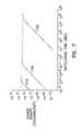
- FIG. 7is a graph that illustrates generally charge density vs. write/erase time for three different embodiments of a floating gate FET.
- FIG. 8is a cross-sectional view, similar to FIG. 2 , but having a larger area control gate—floating gate capacitor than the floating gate—substrate capacitor.
- FIG. 9Ais a schematic diagram, labeled prior art, that illustrates generally a conventional DRAM memory cell.
- FIG. 9Bis a schematic diagram that illustrates generally one embodiment of a floating gate FET memory cell according to the present invention.
- wafer and substrate used in the following descriptioninclude any semiconductor-based structure having an exposed surface with which to form the integrated circuit structure of the invention. Wafer and substrate are used interchangeably to refer to semiconductor structures during processing, and may include other layers that have been fabricated thereupon.
- Both wafer and substrateinclude doped and undoped semiconductors, epitaxial semiconductor layers supported by a base semiconductor or insulator, as well as other semiconductor structures well known to one skilled in the art.
- doped and undoped semiconductorsepitaxial semiconductor layers supported by a base semiconductor or insulator, as well as other semiconductor structures well known to one skilled in the art.
- the following detailed descriptionis, therefore, not to be taken in a limiting sense, and the scope of the present invention is defined only by the appended claims.
- the present inventiondiscloses a memory cell such as, for example, a dynamic electrically alterable programmable read only memory (DEAPROM) cell.
- the memory cellhas a floating electrode, which is defined as an electrode that is “electrically isolated” from conductors and semiconductors by an insulator such that charge storage upon and removal from the floating electrode depends on charge conduction through the insulator.
- the floating electrodeis a floating gate electrode in a floating gate field-effect transistor, such as used in flash electrically erasable and programmable read only memories (EEPROMs).
- EEPROMselectrically erasable and programmable read only memories
- EEPROMselectrically erasable and programmable read only memories
- a capacitor or any other structure having a floating electrode and adjacent insulatorcould also be used according to the techniques of the present invention described below.
- a barrier energy between the floating electrode and the insulatoris lower than the barrier energy between polycrystalline silicon (polysilicon) and silicon dioxide (SiO 2 ), which is approximately 3.3 eV.
- the shorter retention time of data charges on the floating electrode, resulting from the smaller barrier energyis accommodated by refreshing the data charges on the floating electrode.
- the memoryoperates similar to a memory cell in a dynamic random access memory (DRAM).
- FIG. 1is a simplified schematic/block diagram illustrating generally one embodiment of a memory 100 according to one aspect of the present invention, in which reduced barrier energy floating electrode memory cells are incorporated.
- Memory 100is referred to as a dynamic electrically alterable programmable read only memory (DEAPROM) in this application, but it is understood that memory 100 possesses certain characteristics that are similar to DRAMs and flash EEPROMs, as explained below.
- DRAMsdynamic electrically alterable programmable read only memory
- flash EEPROMflash EEPROM
- Memory 100includes a memory array 105 of multiple memory cells 110 .
- Row decoder 115 and column decoder 120decode addresses provided on address lines 125 to access the addressed memory cells in memory array 105 .
- Command and control circuitry 130controls the operation of memory 100 in response to control signals received on control lines 135 from a processor 140 or other memory controller during read, write, refresh, and erase operations.
- Command and control circuitry 130includes a refresh circuit for periodically refreshing the data stored on floating gate transistor or other floating electrode memory cells 110 .
- Voltage control 150provides appropriate voltages to the memory cells during read, write, refresh, and erase operations.
- Memory 100as illustrated in FIG. 1 , has been simplified for the purpose of illustrating the present invention and is not intended to be a complete description. Only the substantial differences between DEAPROM memory 100 and conventional DRAM and flash EEPROM memories are discussed below.
- FIG. 2is a cross-sectional view that illustrates generally, by way of example, but not by way of limitation, one floating gate transistor embodiment of a memory cell 110 .
- Other structural arrangements of floating gate transistorsare included within the present invention.
- any memory cellsthat incorporate a floating electrode (such as a floating electrode capacitor) having, at an interface between the floating electrode an adjacent insulator, a barrier energy that is less than the barrier energy at a polysilicon-SiO 2 interface.
- memory cell 110includes a floating gate FET 200 , which is illustrated as an n-channel FET, but understood to include a p-channel FET embodiment as well.
- FET 200includes a source 205 , a drain 210 , a floating gate 215 electrode, and a control gate 220 electrode.
- a gate insulator 225is interposed between floating gate 215 and substrate 230 .
- An intergate insulator 235is interposed between floating gate 215 and control gate 220 .
- substrate 230is a bulk semiconductor, such as silicon.
- substrate 230includes a thin semiconductor surface layer formed on an underlying insulating portion, such as in a semiconductor-on-insulator (SOI) or other thin film transistor technology.
- Source 205 and drain 210are formed by conventional complementary metal-oxide-semiconductor (CMOS) processing techniques.
- Source 205 and drain 210are separated by a predetermined length for forming an inversion channel 240 therebetween.
- CMOScomplementary metal-oxide-semiconductor
- FIG. 3is an energy band diagram that illustrates generally the conduction band energy levels in floating gate 215 , gate insulator 225 , and substrate 230 .
- Electron affinities ⁇ 215 , ⁇ 225 , and ⁇ 230describe floating gate 215 , gate insulator 225 , and substrate 230 , respectively, when measured with respect to a vacuum level 300 .
- a barrier energy ⁇ GIwhich describes the barrier energy at the interface between floating gate 215 and gate insulator 225 , is given by a difference in electron affinities, as illustrated in Equation 1.
- ⁇ GI⁇ 215 ⁇ 225 (1)
- a barrier energy ⁇ SGwhich describes the barrier energy at the interface between substrate 230 and gate insulator 225 , is given by a difference in electron affinities, as illustrated in Equation 2.
- ⁇ SG⁇ 230 ⁇ 225 (2)
- Silicon (monocrystalline or polycrystalline Si)has an electron affinity ⁇ 215 ⁇ 4.2 eV.
- Silicon dioxide (SiO 2 )has an electron affinity, ⁇ 225 , of about 0.9 eV.
- the resulting barrier energy at a conventional Si—SiO 2 interface between a floating gate and a gate insulatoris approximately equal to 3.3 eV.
- One aspect of the present inventionprovides a barrier energy ⁇ GI that is less than the 3.3 eV barrier energy of a conventional Si—SiO 2 interface.
- the interface between floating gate 215 and gate insulator 225provides a smaller barrier energy ⁇ GI than the 3.3 eV barrier energy at an interface between polysilicon and silicon dioxide, such as by an appropriate selection of the material composition of one or both of floating gate 215 and gate insulator 225 .
- the smaller barrier energy ⁇ GIis obtained by forming floating gate 215 from a material having a smaller electron affinity ⁇ 215 than polysilicon.
- polycrystalline or microcrystalline silicon carbide (SiC)is used as the material for forming floating gate 215 .
- the smaller barrier energy ⁇ GIis obtained by forming gate insulator 225 from a material having a higher electron affinity ⁇ 225 than SiO 2 .
- amorphous SiCis used as the material for forming gate insulator 225 .
- the smaller barrier energy ⁇ GIis obtained by a combination of forming floating gate 215 from a material having a smaller electron affinity ⁇ 215 than polysilicon and also forming gate insulator 225 from a material having a higher electron affinity ⁇ 225 than SiO 2 .
- the smaller barrier energy ⁇ GIprovides current conduction across gate insulator 225 that is easier than for a polysilicon-SiO 2 interface.
- the present inventionincludes any mechanism of providing such easier current conduction across gate insulator 225 , including, but not limited to “hot” electron injection, thermionic emission, Schottky emission, Frenkel-Poole emission, and Fowler-Nordheim tunneling.
- Such techniques for transporting charge carriers across an insulator, such as gate insulator 225are all enhanced by providing a smaller barrier energy ⁇ GI according to the techniques of the present invention.
- FIG. 4is a graph illustrating generally barrier energy versus tunneling distance for a conventional polysilicon-SiO 2 interface having a 3.3 eV barrier energy.
- FIG. 4also illustrates barrier energy versus tunneling distance for an interface according to the present invention that has a barrier energy of ⁇ GI ⁇ 1.08 eV, which is selected as an illustrative example, and not by way of limitation.
- the smaller barrier energy ⁇ GIreduces the energy to which the electrons must be excited to be stored on or removed from the floating gate 215 , such as by thermal emission over the barrier.
- the smaller barrier energy ⁇ GIalso reduces the distance that electrons have to traverse, such as by Fowler-Nordheim tunneling, to be stored upon or removed from floating gate 215 .
- “do”represents the tunneling distance of a conventional floating gate transistor due to the 3.3 eV barrier energy represented by the dashed line “OLD”.
- the tunneling distance “dn”corresponds to a floating gate transistor according to the present invention and its smaller barrier energy, such as ⁇ GI ⁇ 1.08 eV, for example, represented by the dashed line “NEW”.
- Even a small reduction in the tunneling distanceresults in a large increase in the tunneling probability, as described below, because the tunneling probability is an exponential function of the reciprocal of the tunneling distance.
- Equation 3The Fowler-Nordheim tunneling current density in gate insulator 225 illustrated approximately by Equation 3 below.
- JAE 2 e ( ⁇ B/E) (3)
- Equation 3J is the current density in units of amperes/cm 2
- Eis the electric field in gate insulator 225 in units of volts/cm
- a and Bare constants, which are particular to the material of gate insulator 225 , that depend on the effective electron mass in the gate insulator 225 material and on the barrier energy ⁇ GI .
- the constants A and Bscale with the barrier energy ⁇ GI , as illustrated approximately by Equations 4 and 5.
- One aspect of the present inventionincludes selecting a smaller barrier energy ⁇ GI such as, by way of example, but not by way of limitation, ⁇ GI ⁇ 1.08 eV.
- the constants A and B for ⁇ GI ⁇ 1.08 eVcan be extrapolated from the constants A and B for the 3.3 eV polysilicon-SiO 2 barrier energy using Equations 4 and 5.
- FIG. 5is a graph that illustrates generally the relationship between Fowler-Nordheim tunneling current density vs. the barrier energy ⁇ GI , such as at various parameterized values E 1 ⁇ E 2 ⁇ E 3 of an electric field in gate insulator 225 .
- the tunneling current densityincreases as electric field is increased.
- the tunneling currentalso increases by orders of magnitude as the barrier energy ⁇ GI is decreased, such as by selecting the materials for floating gate 215 and gate insulator 225 or otherwise reducing the barrier energy ⁇ GI according to the techniques of the present invention.
- FIG. 5is a graph that illustrates generally the relationship between Fowler-Nordheim tunneling current density vs. the barrier energy ⁇ GI , such as at various parameterized values E 1 ⁇ E 2 ⁇ E 3 of an electric field in gate insulator 225 .
- the tunneling current densityincreases as electric field is increased.
- the tunneling currentalso increases by orders of magnitude as the barrier energy ⁇ GI is decreased, such as
- FIG. 5illustrates a comparison between tunneling current densities at the 3.3 eV barrier energy of a conventional polysilicon-SiO 2 interface and at the illustrative example barrier energy ⁇ GI ⁇ 1.08 eV for which constants A and B were extrapolated above. Reducing the 3.3 eV barrier energy to ⁇ GI ⁇ 1.08 eV increases the tunneling current density by several orders of magnitude.
- FIG. 6is a conceptual diagram, using rough order of magnitude estimates, that illustrates generally how the barrier energy affects the time needed to perform write and erase operations by Fowler-Nordheim tunneling for a particular voltage, such as across gate insulator 225 .
- FIG. 6also illustrates how the barrier energy affects data charge retention time, such as on floating gate 215 at a temperature of 250 degrees Celsius.
- Both write and erase time 600 and data charge retention time 605are decreased by orders of magnitude as the barrier energy is decreased, according to the present invention, from the conventional polysilicon-SiO 2 interface barrier energy of 3.3 eV to the illustrative example lower barrier energy ⁇ GI ⁇ 1.08 eV for which constants A and B were extrapolated above.
- the lower barrier energy ⁇ GI and increased tunneling currentadvantageously provides faster write and erase times. This is particularly advantageous for “flash” EEPROMs or DEAPROMs in which many floating gate transistor memory cells must be erased simultaneously, requiring a longer time to transport the larger quantity of charge.
- flash EEPROMs or DEAPROMsin which many floating gate transistor memory cells must be erased simultaneously, requiring a longer time to transport the larger quantity of charge.
- the simultaneous erasure of a block of memory cellsrequires a time that is on the order of milliseconds.
- the write and erase time of the floating gate FET 200is illustrated approximately by Equation 6.
- Equation 6t is the write/erase time, J 225 and J 235 are the respective tunneling current densities in gate dielectric 225 and intergate dielectric 235 , Q is the charge density in Coulombs/cm 2 on floating gate 215 . Equation 6 is evaluated for a specific voltage on control gate 220 using Equations 7 and 8.
- E 225V 220 [ d 225 + d 235 ⁇ ( ⁇ 225 ⁇ 235 ) ] - Q [ ⁇ 225 + ⁇ 235 ⁇ ( d 225 d 235 ) ] ( 7 )
- E 235V 220 [ d 235 + d 225 ⁇ ( ⁇ 235 ⁇ 225 ) ] + Q [ ⁇ 235 + ⁇ 225 ⁇ ( d 235 d 225 ) ] ( 8 )
- V 220is the voltage on control gate 220
- E 225 and E 235are the respective electric fields in gate insulator 225 and intergate insulator 235
- d 225 and d 235are the respective thicknesses of gate insulator 225 and intergate insulator 235
- ⁇ 225 and ⁇ 235are the respective permittivities of gate insulator 225 and intergate insulator 235 .
- FIG. 7is a graph that illustrates generally charge density vs. write/erase time for three different embodiments of the floating gate FET 200 , each of which have a polysilicon floating gate 215 , by way of illustrative example.
- Line 700illustrates generally, by way of example, but not by way of limitation, the charge density vs. write/erase time obtained for a floating gate FET 200 having a 100 ⁇ SiO 2 gate insulator 225 and a 150 ⁇ SiO 2 (or thinner oxynitride equivalent capacitance) intergate insulator 235 .
- Line 705is similar to line 700 in all respects except that line 705 illustrates a floating gate FET 200 in which gate insulator 225 comprises a material having a higher electron affinity ⁇ 225 than SiO 2 , thereby providing a lower barrier energy ⁇ GI at the interface between polysilicon floating gate 215 and gate insulator 225 .
- the increased tunneling currentresults in shorter write/erase times than those illustrated by line 700 .
- Line 710is similar to line 705 in all respects except that line 710 illustrates a floating gate FET 200 in which gate insulator 225 has a lower barrier energy ⁇ GI than for line 705 , or intergate insulator 235 has a higher permittivity ⁇ 235 than for line 705 , or control gate 220 has a larger area than floating gate 215 , such as illustrated by way of example by the floating gate FET 800 in the cross-sectional view of FIG. 8 . As seen in FIG.
- the area of a capacitor formed by the control gate 220 , the floating gate 215 , and the intergate insulator 235is larger than the area of a capacitor formed by the floating gate 215 , the gate insulator 225 , and the inversion channel 240 underlying gate insulator 225 .
- the intergate insulator 235can have a higher permittivity than the permittivity of silicon dioxide.
- the barrier energy ⁇ GIcan be selected to reduce the write/erase time.
- the barrier energy ⁇ GIis selected to obtain a write/erase time of less than or equal to 1 second, as illustrated in FIG. 7 .
- the barrier energy ⁇ GIis selected to obtain a write/erase time of less than or equal to 1 millisecond, as illustrated in FIG. 7 .
- Other values of write/erase timecan also be obtained by selecting the appropriate value of the barrier energy ⁇ GI .
- the lower barrier energy ⁇ GI and increased tunneling currentalso advantageously reduces the voltage required for writing and erasing the floating gate transistor memory cells 110 .
- conventional polysilicon floating gate transistorstypically require complicated and noisy on-chip charge pump circuits to generate the large erasure voltage, which typically far exceeds other voltages required on the integrated circuit.
- the present inventionallows the use of lower erasure voltages that are more easily provided by simpler on-chip circuits. Reducing the erasure voltage also lowers the electric fields, minimizing reliability problems that can lead to device failure, and better accommodating downward scaling of device dimensions.
- the barrier energy ⁇ GIis selected, as described above, to obtain an erase voltage of less than the 12 Volts required by typical EEPROM memory cells.
- the thickness of the gate insulator 225can be increased from the typical thickness of a silicon dioxide gate insulator to improve reliability or simplify processing, since the lower barrier energy ⁇ GI allows easier transport of charge across the gate insulator 225 by Fowler-Nordheim tunneling.
- the lower barrier energy ⁇ GIalso decreases the data charge retention time of the charge stored on the floating gate 215 , such as from increased thermal excitation of stored charge over the lower barrier ⁇ GI .
- conventional polysilicon floating gates and adjacent SiO 2 insulatorse.g., 90 ⁇ thick
- the barrier energy ⁇ GIis lowered to ⁇ GI ⁇ 1.08 eV by appropriately selecting the composition of the materials of floating gate 215 and gate insulator 225 , as described below.
- an estimated data charge retention timeof approximately 40 seconds at a high temperature, such as 250 degrees C., is obtained.
- the data stored on the DEAPROM floating gate memory cell 110is periodically refreshed at an interval that is shorter than the data charge retention time.
- the datais refreshed every few seconds, such as for an embodiment having a high temperature retention time of approximately 40 seconds for ⁇ GI ⁇ 1.08 eV.
- the exact refresh ratecan be experimentally determined and tailored to a particular process of fabricating the DEAPROM. By decreasing the data charge retention time and periodically refreshing the data, the write and erase operations can be several orders of magnitude faster, as described above with respect to FIG. 7 .
- FIGS. 9A and 9Bare schematic diagrams that respectively illustrate generally a conventional DRAM memory cell and the present invention's floating gate FET 200 embodiment of memory cell 110 .
- the DRAM memory cellincludes an access FET 900 and stacked or trench storage capacitor 905 .
- Datais stored as charge on storage capacitor 905 by providing a control voltage on control line 910 to activate FET 900 for conducting charge.
- Data line 915provides a write voltage to conduct charge across FET 900 for storage on storage capacitor 905 .
- Datais read by providing a control voltage on control line 910 to activate FET 900 for conducting charge from storage capacitor 905 , thereby incrementally changing a preinitialized voltage on data line 915 .
- the resulting small change in voltage on data line 915must be amplified by a sense amplifier for detection.
- the DRAM memory cell of FIG. 9Ainherently provides only a small data signal. The small data signal is difficult to detect.
- the DEAPROM memory cell 110includes floating gate FET 200 , having source 205 coupled to a ground voltage or other reference potential. Data is stored as charge on floating gate 215 by providing a control voltage on control line 920 and a write voltage on data line 925 for hot electron injection or Fowler-Nordheim tunneling. This is similar to conventional EEPROM techniques, but advantageously uses the reduced voltages and/or a shorter write time of the present invention.
- the DEAPROM memory cell 110can be smaller than the DRAM memory cell of FIG. 9A , allowing higher density data storage.
- the leakage of charge from floating gate 215can be made less than the reverse-bias junction leakage from storage capacitor 905 of the DRAM memory cell by tailoring the barrier energy ⁇ GI according to the techniques of the present invention.
- the DEAPROM memory celladvantageously uses the large transconductance gain of the floating gate FET 200 .
- the conventional DRAM memory cell of FIG. 9Aprovides no such gain; it is read by directly transferring the data charge from storage capacitor 905 .
- the DEAPROM memory cell 110is read by placing a read voltage on control line 920 , and detecting the current conducted through FET 200 , such as at data line 925 .
- the current conducted through FET 200changes significantly in the presence or absence of charge stored on floating gate 215 .
- the present inventionadvantageously provides an large data signal that is easy to detect, unlike the small data signal provided by the conventional DRAM memory cell of FIG. 9A
- Equation 9the current for floating gate FET 200 operating in the saturation region can be approximated by Equation 9.
- I D ⁇ ⁇ S1 2 ⁇ ⁇ ⁇ ⁇ C o ⁇ ( W L ) ⁇ ( V G - V T ) 2 ( 9 )
- I DSis the current between drain 210 and source 205
- C 0is the capacitance per unit area of the gate insulator 225
- W/Lis the width/length aspect ratio of FET 200
- V Gis the gate voltage applied to control gate 220
- V Tis the turn-on threshold voltage of FET 200 .
- sufficient chargeis stored on floating gate 215 to change the effective threshold voltage V T by approximately 1.4 Volts, thereby changing the current I DS by approximately 100 microamperes.
- This significant change in currentcan easily be detected, such as by sampling or integrating over a time period of approximately 10 nanoseconds, for example, to obtain a detected data charge signal of 1000 fC.
- the DEAPROM memory cell 110is capable of yielding a detected data charge signal that is approximately an order of magnitude larger than the typical 30 fC to 100 fC data charges typically stored on DRAM stacked or trench capacitors. Since DEAPROM memory cell 110 requires a smaller capacitance value than a conventional DRAM memory cell, DEAPROM memory cell 110 can be made smaller than a conventional DRAM memory cell. Moreover, because the CMOS-compatible DEAPROM storage capacitor is integrally formed as part of the transistor, rather than requiring complex and costly non-CMOS stacked and trench capacitor process steps, the DEAPROM memory of the present invention should be cheaper to fabricate than DRAM memory cells, and should more easily scale downward as CMOS technology advances.
- the present inventionprovides a DEAPROM having a storage element including a gate insulator 225 that includes an amorphous silicon carbide (a-SiC).
- a-SiCamorphous silicon carbide
- a-SiCamorphous silicon carbide
- FIG. 1A block diagram illustrating an exemplary computing environment in accordance with the present invention.
- FIG. 1A block diagram illustrating an exemplary computing environment in accordance with a-SiC gate 225.
- the a-SiC inclusive gate insulator 225provides a higher electron affinity ⁇ 225 than the approximately 0.9 eV electron affinity of SiO 2 .
- the a-SiC inclusive gate insulator 225can provide an electron affinity ⁇ 225 ⁇ 3.24 eV.
- gate insulator 225can also be formed using other techniques.
- gate insulator 225includes a hydrogenated a-SiC material synthesized by ion-implantation of C 2 H 2 into a silicon substrate 230 .
- gate insulator 225includes an a-SiC film that is deposited by laser ablation at room temperature using a pulsed laser in an ultrahigh vacuum or nitrogen environment.
- gate insulator 225includes an a-SiC film that is formed by low-energy ion-beam assisted deposition to minimize structural defects and provide better electrical characteristics in the semiconductor substrate 230 .
- the ion beamcan be generated by electron cyclotron resonance from an ultra high purity argon (Ar) plasma.
- get insulator 225includes an a-SiC film that is synthesized at low temperature by ion beam sputtering in a reactive gas environment with concurrent ion irradiation.
- more than one ion beamsuch as an Ar ion beam, are used.
- a first Ar ion beamis directed at as Si target material to provide a Si flux for forming SiC gate insulator 225 .
- a second Ar ion beamis directed at a graphite target to provide a C flux for forming SiC gate insulator 225 .
- the resulting a-SiC gate insulator 225is formed by sputtering on substrate 230 .
- gate insulator 225includes an SiC film that is deposited on substrate 230 by DC magnetron sputtering at room temperature using a conductive, dense ceramic target.
- gate insulator 225includes a thin a-Si 1-x C x :H film that is formed by HF plasma ion sputtering of a fused SiC target in an Ar—H atmosphere.
- radio frequency (RF) sputteringis used to produce a-SiC films.
- Bandgaps of a-Si, a-SiC, a-Si:H, and a-SiC:Hhave been found to be 1.22 eV, 1.52 eV, 1.87 eV, and 2.2 eV respectively.
- gate insulator 225is formed by chemical vapor deposition (CVD) and includes an a-SiC material.
- gate insulator 225includes a-Si 1-x C x :H deposited by plasma enhanced chemical vapor deposition (PECVD).
- PECVDplasma enhanced chemical vapor deposition
- mixed gases of silane and methanecan be used to form a-Si 1-x C x :H gate insulator 225 .
- the source gascan include silane in methane with additional dilution in hydrogen.
- gate insulator 225includes a clean a-Si 1-x C x material formed by hot-filament assisted CVD.
- gate insulator 225includes a-SiC formed on a crystalline Si substrate 230 by inductively coupled plasma CVD, such as at 450 degrees Celsius, which can yield a-SiC rather than epitaxially grown polycrystalline or microcrystalline SiC.
- the resulting a-SiC inclusive gate insulator 225can provide an electron affinity ⁇ 255 ⁇ 3.24 eV, which is significantly larger than the 0.9 eV electron affinity obtainable from a conventional SiO 2 gate insulator.
- Gate insulator 225can be etched by RF plasma etching using CF 4 O 2 in SF 6 O 2 .
- Self-aligned source 205 and drain 210can then be formed using conventional techniques for forming a FET 200 having a floating (electrically isolated) gate 215 , or in an alternate embodiment, an electrically interconnected (driven) gate.
- the present inventionprovides a DEAPROM having a memory cell 110 that includes a FET 200 having an at least partially crystalline (e.g., monocrystalline, polycrystalline, microcrystalline, nanocrystalline, or combination thereof) SiC floating gate 215 .
- a memory cell 110 that includes a memory storage element having a polycrystalline or microcrystalline SiC floating gate 215is described in Forbes et al.
- U.S. patent application Ser. No. 08/903,486 entitled SILICON CARBIDE GATE TRANSISTORnow U.S. Pat. No. 6,936,849, filed on the same day as the present patent application, and which disclosure is herein incorporated by reference.
- the SiC floating gate 215provides a lower electron affinity ⁇ 3.7 to 3.8 eV and smaller resulting barrier energy ⁇ GI than a polysilicon gate material having an electron affinity ⁇ 215 ⁇ 4.2 eV.
- a barrier energy ⁇ GI ⁇ 2.6 to 2.7 eVobtained using an SiC floating gate 225 , as compared to a barrier energy ⁇ GI ⁇ 3.3 eV for a conventional polysilicon floating gate material at an interface with an SiO 2 gate insulator 225 .
- floating gate 225is formed from a silicon carbide compound Si 1-x C x in which the material composition x is varied.
- a memory storage element having a variable SiC composition floating gate 225is described in Forbes et al.
- an SiC composition of about 0.75 ⁇ 1.0yields an electron affinity of approximately between 1.7 eV ⁇ 215 ⁇ 0.4 eV.
- a barrier 0.8 eV ⁇ GI ⁇ 1.3 eVis obtained.
- floating gate FET 200provides a data charge retention time on the order of seconds.
- floating gate 215is formed by CVD of polycrystalline or microcrystalline SiC, which can be either in situ conductively doped during deposition, or conductively doped during a subsequent ion-implantation step.
- floating gate 215is formed of an SiC film that is deposited using low-pressure chemical vapor deposition (LPCVD).
- LPCVDlow-pressure chemical vapor deposition
- the LPCVD processuses either a hot-wall reactor or a cold-wall reactor with a reactive gas, such as a mixture of Si(CH 3 ) 4 and Ar. Examples of such processes have been disclosed.
- floating gate 215is formed of an SiC film that is deposited using other techniques such as, for example, enhanced CVD techniques known to those skilled in the art including low pressure rapid thermal chemical vapor deposition (LP-RTCVD), or by decomposition of hexamethyl disalene using ArF excimer laser irradiation, or by low temperature molecular beam epitaxy (MBE).
- LP-RTCVDlow pressure rapid thermal chemical vapor deposition
- MBElow temperature molecular beam epitaxy
- Other examples of forming SiC film floating gate 215include reactive magnetron sputtering, DC plasma discharge, ion-beam assisted deposition, ion-beam synthesis of amorphous SiC films, laser crystallization of amorphous SiC, laser reactive ablation deposition, and epitaxial growth by vacuum anneal.
- the conductivity of the SiC film of floating gate 215can be changed by ion implantation during subsequent process steps, such as during the self-aligned formation of source/drain
- SiC filmis patterned using standard techniques and is etched using plasma etching, reactive ion etching (RIE) or a combination of these or other suitable methods.
- RIEreactive ion etching
- the SiC filmcan be etched by RIB in a distributed cyclotron resonance reactor using a SF 6 /O 2 gas mixture using SiO 2 as a mask with a selectivity of 6.5. Such process is known in the art and is disclosed.
- the SiC filmcan be etched by RIB using the mixture SF 6 and O 2 and F 2 /Ar/O 2 .
- etch rate of the SiC filmcan be significantly increased by using magnetron enhanced RIB.
- Self-aligned source 205 and drain 210 regionscan then be formed using conventional techniques for forming a FET 200 having a floating (electrically isolated) gate 215 , or in an alternate embodiment, an electrically interconnected (driven) gate.
- the present inventionprovides a DEAPROM having a memory cell 110 that includes a FET 200 having an at least partially crystalline (e.g., monocrystalline, polycrystalline, microcrystalline, or nanocrystalline) silicon oxycarbide (SiOC) floating gate 215 .
- a memory cell 110that includes a storage element having a polycrystalline or microcrystalline SiOC floating gate 215 is described in Forbes et al.
- U.S. patent application Ser. No. 08/902,132 entitled TRANSISTOR WITH SILICON OXYCARBIDE GATE AND METHODS OF FABRICATION AND USEnow U.S. Pat. No. 5,886,368, filde on the same day as the present patent application, and which disclosure is herein incorporated by reference.
- a material composition w of the SiO (2-2w) C w floating gate 215is selected such that floating gate 215 provides a lower electron affinity approximately between 0.9 eV ⁇ 215 ⁇ 3.7 eV and smaller resulting barrier energy ⁇ GI than a polysilicon gate material having an electron affinity ⁇ 215 ⁇ 4.2 eV.
- a barrier energy approximately between 0 eV ⁇ GI ⁇ 2.8 eVis obtained for an SiOC floating gate 215 as the SiOC composition w varies between w ⁇ 1 (i.e., approximately SiC) and w ⁇ 0 (i.e., approximately SiO 2 ).
- a conventional polysilicon floating gate materialprovides a barrier energy ⁇ GI ⁇ 3.3 eV at an interface with an SiO 2 gate insulator 225 .
- floating gate 215is formed of a monocrystalline, polycrystalline, microcrystalline, or nanocrystalline, SiOC thin film that is CVD deposited, such as by a Two Consecutive Decomposition and Deposition Chamber (TCDDC) system.
- CVDTwo Consecutive Decomposition and Deposition Chamber
- the SiOC filmis deposited using other techniques such as, for example, low pressure chemical vapor deposition (LPCVD), or enhanced CVD techniques known to those skilled in the art including low pressure rapid thermal chemical vapor deposition (LP-RTCVD).
- LPCVDlow pressure chemical vapor deposition
- LP-RTCVDlow pressure rapid thermal chemical vapor deposition
- the conductivity of the SiOC film floating gate 215can be changed by ion implantation during subsequent process steps, such as during the self-aligned formation of source/drain regions for the n-channel and p-channel FETs.
- the SiOC filmcan be patterned and etched, together with the underlying gate insulator 225 , such as by using plasma etching, reactive ion etching (RIE) or a combination of these or other suitable methods.
- RIEreactive ion etching
- the etch rate of SiOC filmcan be significantly increased by using magnetron enhanced RIE.
- the present inventionprovides a DEAPROM having a memory cell 110 including a FET 200 having an at least partially crystalline (e.g., monocrystalline, polycrystalline, microcrystalline, nanocrystalline, or combination thereof) gallium nitride (GaN) or gallium aluminum nitride (GaAlN) floating gate 215 .
- a memory storage element having a GaN or GaAlN floating gate 215is described in Forbes et al.
- U.S. patent application Ser. NO. 08/902,098 entitled DEAPROM AND TRANSISTOR WITH GALLIUM NITRIDE OR GALLIUM ALUMINUM NITRIDE GATEnow U.S. patent No. 6,031,263, filed on the same day as the present patent application, and which disclosure is herein incorporated by reference.
- a composition ⁇ of a polycrystalline Ga 1 ⁇ Al ⁇ N floating gate 215is selected approximately between 0 ⁇ 1 to obtain a desired barrier energy, as described below.
- the GaAlN floating gate 225provides a lower electron affinity than polysilicon.
- the GaAlN floating gate 225 electron affinitycan be approximately between 0.6 eV ⁇ 215 ⁇ 2.7 eV as the GaAlN composition variable ⁇ is decreased from 1 to 0.
- the GaAlN floating gate 215provides a smaller resulting barrier energy ⁇ GI than a polysilicon gate material having an electron affinity ⁇ 215 ⁇ 4.2 eV.
- a barrier energy approximately between ⁇ 0.3 eV ⁇ GI ⁇ 1.8 eVis obtained using an GaAlN floating gate 215 as the GaAlN composition ⁇ varies between ⁇ 1 (i.e., approximately AlN) and ⁇ 0 (i.e., approximately GaN).
- a conventional polysilicon floating gate materialprovides a barrier energy ⁇ GI ⁇ 3.3 eV at an interface with an SiO 2 gate insulator 225 .
- substrate 230is bulk silicon, although other bulk semiconductor and semiconductor-on-insulator (SOI) materials could also be used for substrate 230 such as, for example, sapphire, gallium arsenide (GaAs), GaN, AlN, and diamond.
- gate insulator 225is SiO 2 , although other dielectric materials could also be used for gate insulator 225 , as described above, such as amorphous insulating GaN (a-GaN), and amorphous insulating AlN (a-AlN).
- the FET 200 using a GaAlN floating gate 215has mobility and turn-on threshold voltage (V T ) magnitude parameters that are advantageously influenced less by charge at SiO 2 -GaAlN interface surface states than at a conventional SiO 2 —polysilicon interface.
- V Tturn-on threshold voltage
- floating gate 215is formed of a polycrystalline, microcrystalline, or nanocrystalline, GaN thin film that is CVD deposited on a thin (e.g., 500 ⁇ thick) AlN buffer layer, such as by metal organic chemical vapor deposition (MOCVD), which advantageously yields improved crystal quality and reduced microscopic fluctuation of crystallite orientation.
- MOCVDmetal organic chemical vapor deposition
- floating gate 215is formed from a GaN film grown in a horizontal reactor operating at atmospheric pressure.
- Trimethyl gallium (TMG), trimethylaluminum (TMA), and ammonia (NH 3 )are used as source gases, and hydrogen (H 2 ) is used as a carrier gas.
- the TMG, TNM, and NH 3are mixed just before the reactor, and the mixture is fed at high velocity (e.g., 110 cm/s) to a slanted substrate 230 through a delivery tube.
- the desired GaAlN composition ⁇is obtained by controlling the concentration ratio of TMG to TMA.
- a 500 ⁇ AlN buffer layeris obtained by growth at 600 degrees Celsius at a deposition rate of 100 ⁇ /minute for approximately 5 minutes, then a epitaxial crystalline or polycrystalline layer of GaN is deposited at 1000 degrees Celsius.
- PEMBEplasma-enhanced molecular beam epitaxy
- ECRelectron cyclotron resonance
- the background pressure in the MBE chamberis typically less than 10 ⁇ 10 torr.
- Ga flux(e.g., 99.99999% pure) is supplied by a conventional Knudsen effusion cell.
- the semiconductor substrates 230are heated to a temperature of approximately 850 degrees Celsius, and exposed to a nitrogen plasma (e.g., 35 Watt plasma power level) to clean the surface of the substrate 230 and form a thin AlN layer thereupon.
- the temperatureis then lowered to approximately 550 degrees Celsius for growth of a thin (e.g., 300 ⁇ ) GaN buffer layer (e.g., using 20 Watt plasma power level for growth in a low active nitrogen overpressure environment).
- the temperatureis then increased, such as to approximately 800 degrees Celsius, to form the remainder of the GaN or GaAlN film forming floating gate 225 , such as at a deposition rate of approximately 0.22 microns/hour.
- Each memory cell described hereinhas a floating electrode, such as a floating gate electrode in a floating gate field-effect transistor.
- a barrier energy between the floating electrode and the insulatoris lower than the barrier energy between polysilicon and SiO 2 , which is approximately 3.3 eV.
- Each memory cellalso provides large transconductance gain, which provides a more easily detected signal and reduces the required data storage capacitance value.
- the shorter retention time of data charges on the floating electrode, resulting from the smaller barrier energyis accommodated by refreshing the data charges on the floating electrode. By decreasing the data charge retention time and periodically refreshing the data, the write and erase operations can be several orders of magnitude faster.
- each memoryoperates similar to a memory cell in DRAM, but avoids the process complexity, additional space needed, and other limitations of forming stacked or trench DRAM capacitors.
Landscapes
- Non-Volatile Memory (AREA)
- Semiconductor Memories (AREA)
Abstract
Description
- 1. S. M. Sze, “Physics of Semiconductor Devices,” John Wiley & Sons, New York (1969), p. 496.
- 2. S. R. Pollack et al., “Electron Transport Through Insulating Thin Films,” Applied Solid State Science, Vol. 1, Academic Press, New York, (1969), p. 354.
- 3. D. A. Baglee. “Characteristics and Reliability of 100 Å Oxides,” Proc. 22nd Reliability Symposium, (1984), p. 152.
- 4. G. Comapagnini et al. “Spectroscopic Characterization of Annealed Si1-xCxFilms Synthesized by Ion Implantation,” J. of Materials Research, Vol. 11, No. 9, pp. 2269–73, (1996).
- 5. A. L. Yee et al. “The Effect of Nitrogen on Pulsed Laser Deposition of Amorphous Silicon Carbide Films: Properties and Structure,” J. Of Materials Research, Vol. 11, No. 8, pp. 1979–86 (1996).
- 6. C. D. Tucker et al. “Ion-beam Assisted Deposition of Nonhydrogenated a-Si:C films,” Canadian J. Of Physics. Vol. 74, No. 3–4. pp. 97–10 1 (1996).
- 7. H. Zhang et al., “Ion-beam Assisted Deposition of Si-Carbide Films,” Thin Solid Films, Vol. 260, No. 1, pp. 32–37 (1995).
- 8. S. P. Baker et al. “D-C Magnetron Sputtered Silicon Carbide,” Thin Films, Stresses and Mechanical Properties V. Symposium, pp. Xix+901, 227–32 (1995).
- 9. N. N. Svirkova et al. “Deposition Conditions and Density-of-States Spectrum of a-Si1-xCx:H Films Obtained by Sputtering,” Semiconductors, Vol. 28, No. 12, pp. 1164–9 (1994).
- 10. Y. Suzaki et al. “Quantum Size Effects of a-Si(:H)/a-SiC(:H) Multilayer Films Prepared by RF Sputtering,” J. Of Japan Soc. Of Precision Engineering, Vol. 60, No. 3, pp. 110–18 (1996).
- 11. I. Pereyra et al. “Wide Gap a-Si1-xCx:H Thin Films Obtained Under Starving Plasma Deposition Conditions.” J. Of Non-crystalline Solids, Vol. 201. No. 1–2, pp. 110–118 (1995).
- 12. A. S. Kumbhar et al. “Growth of Clean Amorphous Silicon Carbon Alloy Films By Hot-Filament Assisted Chemical Vapor Deposition Technique,” Appl. Phys. Letters, Vol. 66, No. 14, pp. 1741–3 (1995).
- 13. J. H. Thomas et al. “Plasma Etching and Surface Analysis of a-SiC:H Films Deposited by Low Temperature Plasma Enhanced Vapor Deposition,” Gas-phase and Surface Chemistry in Electronic Materials Processing Symposium, Materials Research Soc., pp. Xv+556, 445–50 (1994).
- 14. Y. Yamaguchi et al., “Properties of Heteroepitaxial 3C-SiC Films Grown by LPCVD”, in the 8th International Conference on Solid-State Sensors and Actuators and Eurosensors IX, Digest of Technical Papers, page 3. vol. (934+1030+85), pages 190–3, Vol. 2, 1995.
- 15. M. Andrieux. et al., “Interface and Adhesion of PECVD SiC Based Films on Metals”, in supplement Le Vide Science, Technique et Applications, (France), No. 279, pages 212–214, 1996.
- 16. F. Lanois, entitled “Angle Etch Control for Silicon Power Devices”, which appeared in Applied Physics Letters, Vol 69, No. 2, pages 236–238, July 1996.
- 17. N. J. Dartnell, et al., entitled “Reactive Ion Etching of Silicon Carbide” in Vacuum. Vol. 46, No. 4, pages 349–355, 1955.
- 18. R. Martins et al., “Transport Properties of Doped Silicon Oxycarbide Microcrystalline Films Produced By Spatial Separation Techniques,” Solar Energy Materials and Solar Cells, Vol. 41–42, pp. 493–517, June 1996.
- 19. R. Martins et al., “Wide band-gap microcrystalline silicon thin films,” Diffusion and Defect Data Part B (Solid State Phenomena), Vol. 44–46, Pt. 2, pp. 299–346, 1995.
- 20. V. M. Bermudez et al. “The Growth and Properties of Al and AlN films on GaN” J. Appl. Physics, Vol. 79, No. 1, pp. 110–119 (1996).
- 21. I. Akasaki et al. “Effects of AlN Buffer Layer on Crystallographic Structure and On Electrical and Optical Properties of GaN and Ga1-xAlxN Films Grown on Sapphire Substrate by MOVPE,” J. Of Crystal Growth, Vol. 98, pp. 209–19, North Holland, Amsterdam (1989).
ΦGI=χ215−χ225 (1)
A barrier energy ΦSG, which describes the barrier energy at the interface between
ΦSG=χ230−χ225 (2)
Silicon (monocrystalline or polycrystalline Si) has an electron affinity χ215≈4.2 eV. Silicon dioxide (SiO2) has an electron affinity, χ225, of about 0.9 eV. The resulting barrier energy at a conventional Si—SiO2interface between a floating gate and a gate insulator is approximately equal to 3.3 eV. One aspect of the present invention provides a barrier energy ΦGIthat is less than the 3.3 eV barrier energy of a conventional Si—SiO2interface.
J=AE2e(−B/E) (3)
In Equation 3, J is the current density in units of amperes/cm2, E is the electric field in
Aα(1/ΦGI) (4)
Bα(1/ΦGI) (5)
For a conventional floating gate FET having a 3.3 eV barrier energy at the interface between the polysilicon floating gate and the SiO2gate insulator, A=5.5×10⁻¹⁶amperes/volt2and B=7.07×10⁷Volts/cm. One aspect of the present invention includes selecting a smaller barrier energy ΦGIsuch as, by way of example, but not by way of limitation, ΦGI≈1.08 eV. The constants A and B for ΦGI≈1.08 eV can be extrapolated from the constants A and B for the 3.3 eV polysilicon-SiO2barrier energy using Equations 4 and 5. The barrier energy ΦGI≈1.08 eV yields the resulting constants A=1.76×10⁻¹⁵amperes/volt2and B=1.24×10⁷Volts/cm.
For a conventional floating gate FET having a 3.3 eV barrier energy at the interface between the polysilicon floating gate and the SiO2gate insulator, A=5.5×10⁻¹⁶amperes/Volt2and B=7.07×10⁷Volts/cm, as disclosed in D. A. Baglee, “Characteristics and Reliability of 100 Å Oxides,” Proc. 22nd Reliability Symposium, (1984), p. 152. One aspect of the present invention includes selecting a smaller barrier energy ΦGIsuch as, by way of example, but not by way of limitation, ΦGI≈1.08 eV. The constants A and B for ΦGI≈1.08 eV can be extrapolated from the constants A and B for the 3.3 eV polysilicon-SiO2barrier energy using Equations 4 and 5. The barrier energy ΦGI26 1.08 eV yields the resulting constants A=1.76×10⁻¹⁵amperes/Volt2and B=1.24×10⁷Volts/cm.
In Equation 6, t is the write/erase time, J225and J235are the respective tunneling current densities in
In
In Equation 9, IDSis the current between
Claims (53)
Priority Applications (1)
| Application Number | Priority Date | Filing Date | Title |
|---|---|---|---|
| US10/231,687US7169666B2 (en) | 1997-07-29 | 2002-08-29 | Method of forming a device having a gate with a selected electron affinity |
Applications Claiming Priority (2)
| Application Number | Priority Date | Filing Date | Title |
|---|---|---|---|
| US08/902,133US7154153B1 (en) | 1997-07-29 | 1997-07-29 | Memory device |
| US10/231,687US7169666B2 (en) | 1997-07-29 | 2002-08-29 | Method of forming a device having a gate with a selected electron affinity |
Related Parent Applications (1)
| Application Number | Title | Priority Date | Filing Date |
|---|---|---|---|
| US08/902,133DivisionUS7154153B1 (en) | 1997-07-29 | 1997-07-29 | Memory device |
Publications (2)
| Publication Number | Publication Date |
|---|---|
| US20030001191A1 US20030001191A1 (en) | 2003-01-02 |
| US7169666B2true US7169666B2 (en) | 2007-01-30 |
Family
ID=25415344
Family Applications (4)
| Application Number | Title | Priority Date | Filing Date |
|---|---|---|---|
| US08/902,133Expired - Fee RelatedUS7154153B1 (en) | 1997-07-29 | 1997-07-29 | Memory device |
| US10/231,687Expired - Fee RelatedUS7169666B2 (en) | 1997-07-29 | 2002-08-29 | Method of forming a device having a gate with a selected electron affinity |
| US10/461,593Expired - Fee RelatedUS7242049B2 (en) | 1997-07-29 | 2003-06-11 | Memory device |
| US10/789,203Expired - Fee RelatedUS7109548B2 (en) | 1997-07-29 | 2004-02-27 | Operating a memory device |
Family Applications Before (1)
| Application Number | Title | Priority Date | Filing Date |
|---|---|---|---|
| US08/902,133Expired - Fee RelatedUS7154153B1 (en) | 1997-07-29 | 1997-07-29 | Memory device |
Family Applications After (2)
| Application Number | Title | Priority Date | Filing Date |
|---|---|---|---|
| US10/461,593Expired - Fee RelatedUS7242049B2 (en) | 1997-07-29 | 2003-06-11 | Memory device |
| US10/789,203Expired - Fee RelatedUS7109548B2 (en) | 1997-07-29 | 2004-02-27 | Operating a memory device |
Country Status (1)
| Country | Link |
|---|---|
| US (4) | US7154153B1 (en) |
Cited By (4)
| Publication number | Priority date | Publication date | Assignee | Title |
|---|---|---|---|---|
| US20090258464A1 (en)* | 2008-04-09 | 2009-10-15 | International Business Machines Corporation | Methods for manufacturing a high voltage junction field effect transistor using a hybrid orientation technology wafer |
| US20090256174A1 (en)* | 2008-04-09 | 2009-10-15 | International Business Machines Corporation | Device structures for a high voltage junction field effect transistor manufactured using a hybrid orientation technology wafer and design structures for a high voltage integrated circuit |
| US20110132448A1 (en)* | 2010-02-08 | 2011-06-09 | Suniva, Inc. | Solar cells and methods of fabrication thereof |
| US20120280233A1 (en)* | 2011-05-03 | 2012-11-08 | Jae Hoon Lee | Nitride-based heterostructure field effect transistor having high efficiency |
Families Citing this family (57)
| Publication number | Priority date | Publication date | Assignee | Title |
|---|---|---|---|---|
| US8253183B2 (en) | 2001-06-28 | 2012-08-28 | Samsung Electronics Co., Ltd. | Charge trapping nonvolatile memory devices with a high-K blocking insulation layer |
| US7253467B2 (en)* | 2001-06-28 | 2007-08-07 | Samsung Electronics Co., Ltd. | Non-volatile semiconductor memory devices |
| US20060180851A1 (en)* | 2001-06-28 | 2006-08-17 | Samsung Electronics Co., Ltd. | Non-volatile memory devices and methods of operating the same |
| US7473959B2 (en)* | 2001-06-28 | 2009-01-06 | Samsung Electronics Co., Ltd. | Non-volatile semiconductor memory devices and methods of fabricating the same |
| DE10228768A1 (en)* | 2001-06-28 | 2003-01-16 | Samsung Electronics Co Ltd | Non-volatile floating trap storage device comprises a semiconductor substrate, a tunnel insulation layer on the substrate, a charge storage layer, a barrier insulation layer, and a gate electrode |
| US7009663B2 (en) | 2003-12-17 | 2006-03-07 | Planar Systems, Inc. | Integrated optical light sensitive active matrix liquid crystal display |
| US7053967B2 (en) | 2002-05-23 | 2006-05-30 | Planar Systems, Inc. | Light sensitive display |
| AU2002336341A1 (en) | 2002-02-20 | 2003-09-09 | Planar Systems, Inc. | Light sensitive display |
| US7224024B2 (en)* | 2002-08-29 | 2007-05-29 | Micron Technology, Inc. | Single transistor vertical memory gain cell |
| US6838723B2 (en)* | 2002-08-29 | 2005-01-04 | Micron Technology, Inc. | Merged MOS-bipolar capacitor memory cell |
| DE10248722A1 (en)* | 2002-10-18 | 2004-05-06 | Infineon Technologies Ag | Integrated circuit arrangement with capacitor and manufacturing process |
| US6804142B2 (en)* | 2002-11-12 | 2004-10-12 | Micron Technology, Inc. | 6F2 3-transistor DRAM gain cell |
| US20080084374A1 (en) | 2003-02-20 | 2008-04-10 | Planar Systems, Inc. | Light sensitive display |
| US6956256B2 (en)* | 2003-03-04 | 2005-10-18 | Micron Technology Inc. | Vertical gain cell |
| JP4382748B2 (en)* | 2003-03-19 | 2009-12-16 | 独立行政法人科学技術振興機構 | Semiconductor crystal growth method |
| US6936518B2 (en)* | 2004-01-21 | 2005-08-30 | Intel Corporation | Creating shallow junction transistors |
| US7773139B2 (en)* | 2004-04-16 | 2010-08-10 | Apple Inc. | Image sensor with photosensitive thin film transistors |
| US7598134B2 (en)* | 2004-07-28 | 2009-10-06 | Micron Technology, Inc. | Memory device forming methods |
| FR2881272B1 (en)* | 2005-01-27 | 2007-08-10 | Commissariat Energie Atomique | ELABORATION OF A TUNNEL OXIDE FOR THE MANUFACTURE OF A NON-VOLATILE MEMORY IN LOW TEMPERATURE FLOTOX TECHNOLOGY |
| US20070045707A1 (en)* | 2005-08-31 | 2007-03-01 | Szu-Yu Wang | Memory device and manufacturing method thereof |
| US20080258133A1 (en)* | 2005-10-29 | 2008-10-23 | Samsung Electronics Co., Ltd. | Semiconductor Device and Method of Fabricating the Same |
| JP5583344B2 (en)* | 2005-12-09 | 2014-09-03 | セムイクウィップ・インコーポレーテッド | System and method for manufacturing semiconductor devices by implantation of carbon clusters |
| US7588982B2 (en)* | 2006-08-29 | 2009-09-15 | Micron Technology, Inc. | Methods of forming semiconductor constructions and flash memory cells |
| JP2008066593A (en)* | 2006-09-08 | 2008-03-21 | Toshiba Corp | Nonvolatile semiconductor memory and manufacturing method thereof |
| KR100851553B1 (en)* | 2006-10-02 | 2008-08-11 | 삼성전자주식회사 | Image sensor and method of driving the same |
| US20080105946A1 (en)* | 2006-10-24 | 2008-05-08 | Atmel Corporation | Solid state field emission charge storage |
| US7919402B2 (en)* | 2006-12-06 | 2011-04-05 | Semequip, Inc. | Cluster ion implantation for defect engineering |
| WO2008128039A2 (en)* | 2007-04-11 | 2008-10-23 | Semequip, Inc. | Cluster ion implantation for defect engineering |
| KR101338158B1 (en)* | 2007-07-16 | 2013-12-06 | 삼성전자주식회사 | Non-volatile memory devices and methods of forming the same |
| US20090200494A1 (en)* | 2008-02-11 | 2009-08-13 | Varian Semiconductor Equipment Associates, Inc. | Techniques for cold implantation of carbon-containing species |
| US8003957B2 (en)* | 2008-02-11 | 2011-08-23 | Varian Semiconductor Equipment Associates, Inc. | Ethane implantation with a dilution gas |
| DE102008029385B4 (en)* | 2008-06-23 | 2014-11-27 | Carl Von Ossietzky Universität Oldenburg | A process for producing rare earth metal oxide layers and transition metal oxide layers, use of an apparatus for producing rare earth metal oxide layers and transition metal oxide layers, and use of a metal nitrate |
| CN101620991B (en)* | 2008-07-02 | 2011-08-17 | 中芯国际集成电路制造(上海)有限公司 | Growth of atomic layer deposition epitaxial silicon of TFT flash memory cell |
| CN101621008A (en) | 2008-07-03 | 2010-01-06 | 中芯国际集成电路制造(上海)有限公司 | TFT floating gate memory cell structure |
| US9059302B2 (en)* | 2009-04-06 | 2015-06-16 | Infineon Technologies Ag | Floating gate memory device with at least partially surrounding control gate |
| US8941171B2 (en) | 2010-07-02 | 2015-01-27 | Micron Technology, Inc. | Flatband voltage adjustment in a semiconductor device |
| US20120101731A1 (en)* | 2010-10-21 | 2012-04-26 | Baker Hughes Incorporated | Extending Data Retention of a Data Storage Device Downhole |
| US9310923B2 (en) | 2010-12-03 | 2016-04-12 | Apple Inc. | Input device for touch sensitive devices |
| US9673823B2 (en)* | 2011-05-18 | 2017-06-06 | Semiconductor Energy Laboratory Co., Ltd. | Semiconductor device and method of driving semiconductor device |
| US8928635B2 (en) | 2011-06-22 | 2015-01-06 | Apple Inc. | Active stylus |
| US9329703B2 (en) | 2011-06-22 | 2016-05-03 | Apple Inc. | Intelligent stylus |
| US8638320B2 (en) | 2011-06-22 | 2014-01-28 | Apple Inc. | Stylus orientation detection |
| WO2013010161A2 (en)* | 2011-07-14 | 2013-01-17 | University Of South Florida | Long-term implantable silicon carbide neural interface device using the electrical field effect |
| US9557845B2 (en) | 2012-07-27 | 2017-01-31 | Apple Inc. | Input device for and method of communication with capacitive devices through frequency variation |
| US9176604B2 (en) | 2012-07-27 | 2015-11-03 | Apple Inc. | Stylus device |
| US9652090B2 (en) | 2012-07-27 | 2017-05-16 | Apple Inc. | Device for digital communication through capacitive coupling |
| US10048775B2 (en) | 2013-03-14 | 2018-08-14 | Apple Inc. | Stylus detection and demodulation |
| US10067580B2 (en) | 2013-07-31 | 2018-09-04 | Apple Inc. | Active stylus for use with touch controller architecture |
| CN105242871B (en)* | 2014-06-06 | 2018-06-05 | 华为技术有限公司 | A kind of method for writing data and device |
| US9263586B2 (en) | 2014-06-06 | 2016-02-16 | Taiwan Semiconductor Manufacturing Company, Ltd. | Quantum well fin-like field effect transistor (QWFinFET) having a two-section combo QW structure |
| US10067618B2 (en) | 2014-12-04 | 2018-09-04 | Apple Inc. | Coarse scan and targeted active mode scan for touch |
| US10474277B2 (en) | 2016-05-31 | 2019-11-12 | Apple Inc. | Position-based stylus communication |
| US9953839B2 (en)* | 2016-08-18 | 2018-04-24 | International Business Machines Corporation | Gate-stack structure with a diffusion barrier material |
| GB201907540D0 (en)* | 2019-05-29 | 2019-07-10 | Univ Of Lancaster | Improvements relating to electronic memory devices |
| KR102795919B1 (en) | 2019-12-30 | 2025-04-16 | 삼성전자주식회사 | Capacitor structure, method of manufacturing the same, semiconductor device including the capacitor structure and method of manufacturing the same |
| US12153764B1 (en) | 2020-09-25 | 2024-11-26 | Apple Inc. | Stylus with receive architecture for position determination |
| KR20220091162A (en) | 2020-12-23 | 2022-06-30 | 삼성전자주식회사 | Memory device and method for refreshing operation irrelevant to refresh rate multipliers for temperatatures |
Citations (135)
| Publication number | Priority date | Publication date | Assignee | Title |
|---|---|---|---|---|
| US3792465A (en) | 1971-12-30 | 1974-02-12 | Texas Instruments Inc | Charge transfer solid state display |
| US4019197A (en) | 1975-01-17 | 1977-04-19 | U.S. Philips Corporation | Semiconductor floating gate storage device with lateral electrode system |
| US4113515A (en) | 1975-06-04 | 1978-09-12 | U.S. Philips Corporation | Semiconductor manufacturing method using buried nitride formed by a nitridation treatment in the presence of active nitrogen |
| US4118795A (en) | 1976-08-27 | 1978-10-03 | Texas Instruments Incorporated | Two-phase CCD regenerator - I/O circuits |
| JPS57126175U (en) | 1981-01-27 | 1982-08-06 | ||
| US4384349A (en) | 1979-10-01 | 1983-05-17 | Texas Instruments Incorporated | High density electrically erasable floating gate dual-injection programmable memory device |
| US4460670A (en) | 1981-11-26 | 1984-07-17 | Canon Kabushiki Kaisha | Photoconductive member with α-Si and C, N or O and dopant |
| US4462150A (en) | 1981-11-10 | 1984-07-31 | Tokyo Shibaura Denki Kabushiki Kaisha | Method of forming energy beam activated conductive regions between circuit elements |
| US4473836A (en) | 1982-05-03 | 1984-09-25 | Dalsa Inc. | Integrable large dynamic range photodetector element for linear and area integrated circuit imaging arrays |
| US4507673A (en) | 1979-10-13 | 1985-03-26 | Tokyo Shibaura Denki Kabushiki Kaisha | Semiconductor memory device |
| JPS6024678Y2 (en) | 1980-12-01 | 1985-07-24 | 株式会社ダイフク | Conveyance device using a trolley |
| JPS60242678A (en) | 1984-05-17 | 1985-12-02 | Seiko Epson Corp | semiconductor storage device |
| JPS60184681U (en) | 1984-05-16 | 1985-12-07 | 株式会社 キングジム | slip holder |
| US4598305A (en) | 1984-06-18 | 1986-07-01 | Xerox Corporation | Depletion mode thin film semiconductor photodetectors |
| US4657699A (en) | 1984-12-17 | 1987-04-14 | E. I. Du Pont De Nemours And Company | Resistor compositions |
| JPS6286867U (en) | 1985-11-19 | 1987-06-03 | ||
| JPS62122275U (en) | 1986-01-24 | 1987-08-03 | ||
| US4736317A (en) | 1985-07-17 | 1988-04-05 | Syracuse University | Microprogram-coupled multiple-microprocessor module with 32-bit byte width formed of 8-bit byte width microprocessors |
| US4738729A (en) | 1984-10-19 | 1988-04-19 | Toshihiko Yoshida | Amorphous silicon semiconductor solar cell |
| JPS63128760U (en) | 1987-02-13 | 1988-08-23 | ||
| US4768072A (en) | 1984-01-20 | 1988-08-30 | Fuji Electric Corporate Research And Development Co., Ltd. | Multilayer semiconductor device having an amorphous carbon and silicon layer |
| US4769686A (en) | 1983-04-01 | 1988-09-06 | Hitachi, Ltd. | Semiconductor device |
| JPS63219172A (en) | 1987-03-06 | 1988-09-12 | Hosiden Electronics Co Ltd | Thin-film transistor |
| JPS63181473U (en) | 1987-05-12 | 1988-11-22 | ||
| US4816883A (en) | 1986-07-10 | 1989-03-28 | Sgs Microelettronica S.P.A. | Nonvolatile, semiconductor memory device |
| JPH01115162A (en) | 1987-10-29 | 1989-05-08 | Matsushita Electric Ind Co Ltd | Thin film transistor and its manufacturing method |
| US4841349A (en) | 1984-11-16 | 1989-06-20 | Fujitsu Limited | Semiconductor photodetector device with light responsive PN junction gate |
| US4849797A (en) | 1987-01-23 | 1989-07-18 | Hosiden Electronics Co., Ltd. | Thin film transistor |
| US4893273A (en) | 1985-03-28 | 1990-01-09 | Kabushiki Kaisha Toshiba | Semiconductor memory device for storing image data |
| US4897710A (en) | 1986-08-18 | 1990-01-30 | Sharp Kabushiki Kaisha | Semiconductor device |
| US4929985A (en) | 1988-05-18 | 1990-05-29 | Fujitsu Limited | Compound semiconductor device |
| JPH02203564A (en) | 1989-01-31 | 1990-08-13 | Sharp Corp | Silicon carbide semiconductor device |
| US4980303A (en) | 1987-08-19 | 1990-12-25 | Fujitsu Limited | Manufacturing method of a Bi-MIS semiconductor device |
| US4994401A (en) | 1987-01-16 | 1991-02-19 | Hosiden Electronics Co., Ltd. | Method of making a thin film transistor |
| US5032883A (en) | 1987-09-09 | 1991-07-16 | Casio Computer Co., Ltd. | Thin film transistor and method of manufacturing the same |
| US5049950A (en) | 1987-07-14 | 1991-09-17 | Sharp Kabushiki Kaisha | MIS structure photosensor |
| JPH03222367A (en) | 1990-01-26 | 1991-10-01 | Fujitsu Ltd | Insulated gate type field effect transistor |
| US5111430A (en) | 1989-06-22 | 1992-05-05 | Nippon Telegraph And Telephone Corporation | Non-volatile memory with hot carriers transmitted to floating gate through control gate |
| US5145741A (en) | 1989-06-05 | 1992-09-08 | Quick Nathaniel R | Converting ceramic materials to electrical conductors and semiconductors |
| JPH0456769B2 (en) | 1985-09-27 | 1992-09-09 | Ube Industries | |
| US5189504A (en) | 1989-12-11 | 1993-02-23 | Nippon Telegraph And Telephone Corporation | Semiconductor device of MOS structure having p-type gate electrode |
| EP0291951B1 (en) | 1987-05-22 | 1993-08-04 | Fujitsu Limited | A semiconductor field effect transistor using single crystalline silicon carbide as a gate insulating layer |
| US5235195A (en) | 1990-08-08 | 1993-08-10 | Minnesota Mining And Manufacturing Company | Solid state electromagnetic radiation detector with planarization layer |
| US5260593A (en) | 1991-12-10 | 1993-11-09 | Micron Technology, Inc. | Semiconductor floating gate device having improved channel-floating gate interaction |
| US5293560A (en) | 1988-06-08 | 1994-03-08 | Eliyahou Harari | Multi-state flash EEPROM system using incremental programing and erasing methods |
| US5298796A (en) | 1992-07-08 | 1994-03-29 | The United States Of America As Represented By The Administrator Of The National Aeronautics And Space Administration | Nonvolatile programmable neural network synaptic array |
| JPH0613626Y2 (en) | 1988-12-23 | 1994-04-13 | 有限会社河島農具製作所 | Fertilizer bag holder |
| US5317535A (en) | 1992-06-19 | 1994-05-31 | Intel Corporation | Gate/source disturb protection for sixteen-bit flash EEPROM memory arrays |
| US5336361A (en) | 1990-03-23 | 1994-08-09 | Matsushita Electric Industrial Co., Ltd. | Method of manufacturing an MIS-type semiconductor device |
| JPH06224431A (en) | 1993-01-26 | 1994-08-12 | Sharp Corp | Thin-film transistor and liquid crystal display panel |
| JPH06302828A (en) | 1993-04-14 | 1994-10-28 | Matsushita Electric Ind Co Ltd | Nonvolatile semiconductor memory device |
| US5360491A (en) | 1993-04-07 | 1994-11-01 | The United States Of America As Represented By The United States Department Of Energy | β-silicon carbide protective coating and method for fabricating same |
| US5367306A (en) | 1993-06-04 | 1994-11-22 | Hollon Blake D | GPS integrated ELT system |
| US5366713A (en) | 1992-06-03 | 1994-11-22 | Showa Shell Sekiyu K.K. | Method of forming p-type silicon carbide |
| US5369040A (en) | 1992-05-18 | 1994-11-29 | Westinghouse Electric Corporation | Method of making transparent polysilicon gate for imaging arrays |
| US5371383A (en) | 1993-05-14 | 1994-12-06 | Kobe Steel Usa Inc. | Highly oriented diamond film field-effect transistor |
| US5388069A (en) | 1992-03-19 | 1995-02-07 | Fujitsu Limited | Nonvolatile semiconductor memory device for preventing erroneous operation caused by over-erase phenomenon |
| US5393999A (en) | 1993-02-22 | 1995-02-28 | Texas Instruments Incorporated | SiC power MOSFET device structure |
| US5407845A (en) | 1992-10-15 | 1995-04-18 | Fujitsu Limited | Method of manufacturing thin film transistors in a liquid crystal display apparatus |
| US5409501A (en) | 1991-07-15 | 1995-04-25 | Henkel Kommanditgesellschaft Auf Aktien | Dilutable aluminum triformate tanning agents in the form of highly concentrated, storable aqueous solutions and their use |
| US5415126A (en) | 1993-08-16 | 1995-05-16 | Dow Corning Corporation | Method of forming crystalline silicon carbide coatings at low temperatures |
| US5424993A (en) | 1993-11-15 | 1995-06-13 | Micron Technology, Inc. | Programming method for the selective healing of over-erased cells on a flash erasable programmable read-only memory device |
| US5425860A (en) | 1993-04-07 | 1995-06-20 | The Regents Of The University Of California | Pulsed energy synthesis and doping of silicon carbide |
| US5438211A (en) | 1993-03-31 | 1995-08-01 | Kabushiki Kaisha Toshiba | Charge-transfer device having an improved charge-sensing section |
| US5438544A (en) | 1993-03-19 | 1995-08-01 | Fujitsu Limited | Non-volatile semiconductor memory device with function of bringing memory cell transistors to overerased state, and method of writing data in the device |
| US5441901A (en) | 1993-10-05 | 1995-08-15 | Motorola, Inc. | Method for forming a carbon doped silicon semiconductor device having a narrowed bandgap characteristic |
| JPH07226507A (en) | 1994-02-10 | 1995-08-22 | Fujitsu Ltd | Semiconductor device and manufacturing method thereof |
| US5449941A (en) | 1991-10-29 | 1995-09-12 | Semiconductor Energy Laboratory Co., Ltd. | Semiconductor memory device |
| US5455432A (en) | 1994-10-11 | 1995-10-03 | Kobe Steel Usa | Diamond semiconductor device with carbide interlayer |
| US5465249A (en) | 1991-11-26 | 1995-11-07 | Cree Research, Inc. | Nonvolatile random access memory device having transistor and capacitor made in silicon carbide substrate |
| EP0681333A1 (en) | 1994-04-29 | 1995-11-08 | International Business Machines Corporation | Low voltage memory |
| US5467306A (en) | 1993-10-04 | 1995-11-14 | Texas Instruments Incorporated | Method of using source bias to increase threshold voltages and/or to correct for over-erasure of flash eproms |
| JPH07115191B2 (en) | 1988-02-18 | 1995-12-13 | 松下電器産業株式会社 | Plasma cutting machine |
| US5477485A (en) | 1995-02-22 | 1995-12-19 | National Semiconductor Corporation | Method for programming a single EPROM or FLASH memory cell to store multiple levels of data that utilizes a floating substrate |
| US5493140A (en) | 1993-07-05 | 1996-02-20 | Sharp Kabushiki Kaisha | Nonvolatile memory cell and method of producing the same |
| US5530581A (en) | 1995-05-31 | 1996-06-25 | Eic Laboratories, Inc. | Protective overlayer material and electro-optical coating using same |
| US5546351A (en) | 1991-12-19 | 1996-08-13 | Kabushiki Kaisha Toshiba | Non-volatile semiconductor memory device and memory system using the same |
| US5557122A (en) | 1995-05-12 | 1996-09-17 | Alliance Semiconductors Corporation | Semiconductor electrode having improved grain structure and oxide growth properties |
| US5557114A (en) | 1995-01-12 | 1996-09-17 | International Business Machines Corporation | Optical fet |
| JPH08255878A (en) | 1995-03-16 | 1996-10-01 | Fujitsu Ltd | Floating gate transistor and manufacturing method thereof |
| US5562769A (en) | 1991-12-20 | 1996-10-08 | Kobe Steel Usa, Inc. | Methods of forming diamond semiconductor devices and layers on nondiamond substrates |
| US5604357A (en) | 1994-07-12 | 1997-02-18 | Matsushita Electric Industrial Co., Ltd. | Semiconductor nonvolatile memory with resonance tunneling |
| US5614748A (en) | 1992-06-09 | 1997-03-25 | Sony Corporation | Nonvolatile memory device and process for production of the same |
| US5623160A (en) | 1995-09-14 | 1997-04-22 | Liberkowski; Janusz B. | Signal-routing or interconnect substrate, structure and apparatus |
| US5623442A (en) | 1993-07-13 | 1997-04-22 | Nkk Corporation | Memory cells and memory devices with a storage capacitor of parasitic capacitance and information storing method using the same |
| US5654208A (en) | 1995-04-10 | 1997-08-05 | Abb Research Ltd. | Method for producing a semiconductor device having a semiconductor layer of SiC comprising a masking step |
| US5661312A (en) | 1995-03-30 | 1997-08-26 | Motorola | Silicon carbide MOSFET |
| US5670790A (en) | 1995-09-21 | 1997-09-23 | Kabushikik Kaisha Toshiba | Electronic device |
| US5672889A (en) | 1995-03-15 | 1997-09-30 | General Electric Company | Vertical channel silicon carbide metal-oxide-semiconductor field effect transistor with self-aligned gate for microwave and power applications, and method of making |
| US5698879A (en) | 1994-08-19 | 1997-12-16 | Kabushiki Kaisha Toshiba | Nonvolatile semiconductor memory device |
| US5698869A (en) | 1994-09-13 | 1997-12-16 | Kabushiki Kaisha Toshiba | Insulated-gate transistor having narrow-bandgap-source |
| US5714766A (en) | 1995-09-29 | 1998-02-03 | International Business Machines Corporation | Nano-structure memory device |
| US5719410A (en) | 1993-12-28 | 1998-02-17 | Kabushiki Kaisha Toshiba | Semiconductor device wiring or electrode |
| US5734181A (en) | 1995-09-14 | 1998-03-31 | Kabushiki Kaisha Toshiba | Semiconductor device and manufacturing method therefor |
| US5738731A (en) | 1993-11-19 | 1998-04-14 | Mega Chips Corporation | Photovoltaic device |
| US5740104A (en) | 1997-01-29 | 1998-04-14 | Micron Technology, Inc. | Multi-state flash memory cell and method for programming single electron differences |
| US5754477A (en) | 1997-01-29 | 1998-05-19 | Micron Technology, Inc. | Differential flash memory cell and method for programming |
| US5774400A (en) | 1995-12-26 | 1998-06-30 | Nvx Corporation | Structure and method to prevent over erasure of nonvolatile memory transistors |
| US5786250A (en) | 1997-03-14 | 1998-07-28 | Micron Technology, Inc. | Method of making a capacitor |
| US5798548A (en) | 1995-05-18 | 1998-08-25 | Sanyo Electric Co., Ltd. | Semiconductor device having multiple control gates |
| US5801401A (en) | 1997-01-29 | 1998-09-01 | Micron Technology, Inc. | Flash memory with microcrystalline silicon carbide film floating gate |
| US5808336A (en) | 1994-05-13 | 1998-09-15 | Canon Kabushiki Kaisha | Storage device |
| US5828101A (en)* | 1995-03-30 | 1998-10-27 | Kabushiki Kaisha Toshiba | Three-terminal semiconductor device and related semiconductor devices |
| US5846859A (en) | 1995-03-14 | 1998-12-08 | Samsung Electronics Co., Ltd. | Method for manufacturing a semiconductor memory device having capacitive storage |
| US5858811A (en) | 1994-11-28 | 1999-01-12 | Nec Corporation | Method for fabricating charge coupled device (CCD) as semiconductor device of MOS structure |
| US5861346A (en) | 1995-07-27 | 1999-01-19 | Regents Of The University Of California | Process for forming silicon carbide films and microcomponents |
| US5877041A (en) | 1997-06-30 | 1999-03-02 | Harris Corporation | Self-aligned power field effect transistor in silicon carbide |
| US5886379A (en) | 1996-05-16 | 1999-03-23 | Lg Semicon Co., Ltd. | Semiconductor memory device with increased coupling ratio |
| US5886368A (en) | 1997-07-29 | 1999-03-23 | Micron Technology, Inc. | Transistor with silicon oxycarbide gate and methods of fabrication and use |
| US5886376A (en) | 1996-07-01 | 1999-03-23 | International Business Machines Corporation | EEPROM having coplanar on-insulator FET and control gate |
| US5898197A (en) | 1996-06-06 | 1999-04-27 | Sanyo Electric Co., Ltd. | Non-volatile semiconductor memory devices |
| US5907775A (en) | 1997-04-11 | 1999-05-25 | Vanguard International Semiconductor Corporation | Non-volatile memory device with high gate coupling ratio and manufacturing process therefor |
| US5910665A (en) | 1995-12-29 | 1999-06-08 | Texas Instruments Incorporated | Low capacitance power VFET method and device |
| US5912837A (en) | 1996-10-28 | 1999-06-15 | Micron Technology, Inc. | Bitline disturb reduction |
| US5926740A (en) | 1997-10-27 | 1999-07-20 | Micron Technology, Inc. | Graded anti-reflective coating for IC lithography |
| US5976926A (en) | 1996-11-12 | 1999-11-02 | Micron Technology, Inc. | Static memory cell and method of manufacturing a static memory cell |
| US5990531A (en) | 1995-12-28 | 1999-11-23 | Philips Electronics N.A. Corporation | Methods of making high voltage GaN-AlN based semiconductor devices and semiconductor devices made |
| US6018166A (en) | 1996-12-31 | 2000-01-25 | Industrial Technology Research Institute | Polysilicon carbon source/drain heterojunction thin-film transistor |
| US6031263A (en) | 1997-07-29 | 2000-02-29 | Micron Technology, Inc. | DEAPROM and transistor with gallium nitride or gallium aluminum nitride gate |
| US6034001A (en) | 1991-10-16 | 2000-03-07 | Kulite Semiconductor Products, Inc. | Method for etching of silicon carbide semiconductor using selective etching of different conductivity types |
| US6049091A (en)* | 1996-07-01 | 2000-04-11 | Nec Corporation | High electron mobility transistor |
| US6075259A (en) | 1994-11-14 | 2000-06-13 | North Carolina State University | Power semiconductor devices that utilize buried insulating regions to achieve higher than parallel-plane breakdown voltages |
| US6084248A (en) | 1996-06-28 | 2000-07-04 | Seiko Epson Corporation | Thin film transistor, manufacturing method thereof, and circuit and liquid crystal display device using the thin film transistor |
| US6093937A (en) | 1996-02-23 | 2000-07-25 | Semiconductor Energy Laboratory Co. Ltd. | Semiconductor thin film, semiconductor device and manufacturing method thereof |
| US6099574A (en) | 1996-12-19 | 2000-08-08 | Kabushiki Kaisha Toshiba | Method and apparatus for obtaining structure of semiconductor devices and memory for storing program for obtaining the same |
| US6130147A (en) | 1994-04-07 | 2000-10-10 | Sdl, Inc. | Methods for forming group III-V arsenide-nitride semiconductor materials |
| US6144581A (en) | 1996-07-24 | 2000-11-07 | California Institute Of Technology | pMOS EEPROM non-volatile data storage |
| US6163066A (en) | 1997-02-07 | 2000-12-19 | Micron Technology, Inc. | Porous silicon dioxide insulator |
| US6166768A (en) | 1994-01-28 | 2000-12-26 | California Institute Of Technology | Active pixel sensor array with simple floating gate pixels |
| US6271566B1 (en) | 1997-03-25 | 2001-08-07 | Toshiba Corporation | Semiconductor device having a carbon containing insulation layer formed under the source/drain |
| US6365919B1 (en) | 1998-09-02 | 2002-04-02 | Infineon Technologies Ag | Silicon carbide junction field effect transistor |
| US6835638B1 (en) | 1997-07-29 | 2004-12-28 | Micron Technology, Inc. | Silicon carbide gate transistor and fabrication process |
| US20050146934A1 (en) | 1997-07-29 | 2005-07-07 | Micron Technology, Inc. | Transistor with variable electron affinity gate and methods of fabrication and use |
| US20060017095A1 (en) | 1997-07-29 | 2006-01-26 | Micron Technology, Inc. | Carburized silicon gate insulators for integrated circuits |
| US20060024878A1 (en) | 1997-07-29 | 2006-02-02 | Micron Technology, Inc. | Deaprom having amorphous silicon carbide gate insulator |
Family Cites Families (4)
| Publication number | Priority date | Publication date | Assignee | Title |
|---|---|---|---|---|
| JPS5656677U (en) | 1979-10-02 | 1981-05-16 | ||
| JPS57126175A (en) | 1981-01-29 | 1982-08-05 | Kanegafuchi Chem Ind Co Ltd | Amorphous silicon carbide/amorophous silicon hetero junction optoelectric element |
| JPS60184681A (en) | 1984-03-02 | 1985-09-20 | Sharp Corp | Method for forming amorphous silicon carbide film for coating |
| JPH0613626A (en)* | 1992-06-29 | 1994-01-21 | Oki Electric Ind Co Ltd | Semiconductor memory device |
- 1997
- 1997-07-29USUS08/902,133patent/US7154153B1/ennot_activeExpired - Fee Related
- 2002
- 2002-08-29USUS10/231,687patent/US7169666B2/ennot_activeExpired - Fee Related
- 2003
- 2003-06-11USUS10/461,593patent/US7242049B2/ennot_activeExpired - Fee Related
- 2004
- 2004-02-27USUS10/789,203patent/US7109548B2/ennot_activeExpired - Fee Related
Patent Citations (150)
| Publication number | Priority date | Publication date | Assignee | Title |
|---|---|---|---|---|
| US3792465A (en) | 1971-12-30 | 1974-02-12 | Texas Instruments Inc | Charge transfer solid state display |
| US4019197A (en) | 1975-01-17 | 1977-04-19 | U.S. Philips Corporation | Semiconductor floating gate storage device with lateral electrode system |
| US4113515A (en) | 1975-06-04 | 1978-09-12 | U.S. Philips Corporation | Semiconductor manufacturing method using buried nitride formed by a nitridation treatment in the presence of active nitrogen |
| US4118795A (en) | 1976-08-27 | 1978-10-03 | Texas Instruments Incorporated | Two-phase CCD regenerator - I/O circuits |
| US4384349A (en) | 1979-10-01 | 1983-05-17 | Texas Instruments Incorporated | High density electrically erasable floating gate dual-injection programmable memory device |
| US4507673A (en) | 1979-10-13 | 1985-03-26 | Tokyo Shibaura Denki Kabushiki Kaisha | Semiconductor memory device |
| JPS6024678Y2 (en) | 1980-12-01 | 1985-07-24 | 株式会社ダイフク | Conveyance device using a trolley |
| JPS57126175U (en) | 1981-01-27 | 1982-08-06 | ||
| US4462150A (en) | 1981-11-10 | 1984-07-31 | Tokyo Shibaura Denki Kabushiki Kaisha | Method of forming energy beam activated conductive regions between circuit elements |
| US4460670A (en) | 1981-11-26 | 1984-07-17 | Canon Kabushiki Kaisha | Photoconductive member with α-Si and C, N or O and dopant |
| US4473836A (en) | 1982-05-03 | 1984-09-25 | Dalsa Inc. | Integrable large dynamic range photodetector element for linear and area integrated circuit imaging arrays |
| US4769686A (en) | 1983-04-01 | 1988-09-06 | Hitachi, Ltd. | Semiconductor device |
| US4768072A (en) | 1984-01-20 | 1988-08-30 | Fuji Electric Corporate Research And Development Co., Ltd. | Multilayer semiconductor device having an amorphous carbon and silicon layer |
| JPS60184681U (en) | 1984-05-16 | 1985-12-07 | 株式会社 キングジム | slip holder |
| JPS60242678A (en) | 1984-05-17 | 1985-12-02 | Seiko Epson Corp | semiconductor storage device |
| US4598305A (en) | 1984-06-18 | 1986-07-01 | Xerox Corporation | Depletion mode thin film semiconductor photodetectors |
| US4738729A (en) | 1984-10-19 | 1988-04-19 | Toshihiko Yoshida | Amorphous silicon semiconductor solar cell |
| US4841349A (en) | 1984-11-16 | 1989-06-20 | Fujitsu Limited | Semiconductor photodetector device with light responsive PN junction gate |
| US4657699A (en) | 1984-12-17 | 1987-04-14 | E. I. Du Pont De Nemours And Company | Resistor compositions |
| US4893273A (en) | 1985-03-28 | 1990-01-09 | Kabushiki Kaisha Toshiba | Semiconductor memory device for storing image data |
| US4736317A (en) | 1985-07-17 | 1988-04-05 | Syracuse University | Microprogram-coupled multiple-microprocessor module with 32-bit byte width formed of 8-bit byte width microprocessors |
| JPH0456769B2 (en) | 1985-09-27 | 1992-09-09 | Ube Industries | |
| JPS6286867U (en) | 1985-11-19 | 1987-06-03 | ||
| JPS62122275U (en) | 1986-01-24 | 1987-08-03 | ||
| US4816883A (en) | 1986-07-10 | 1989-03-28 | Sgs Microelettronica S.P.A. | Nonvolatile, semiconductor memory device |
| US4897710A (en) | 1986-08-18 | 1990-01-30 | Sharp Kabushiki Kaisha | Semiconductor device |
| US4994401A (en) | 1987-01-16 | 1991-02-19 | Hosiden Electronics Co., Ltd. | Method of making a thin film transistor |
| US4849797A (en) | 1987-01-23 | 1989-07-18 | Hosiden Electronics Co., Ltd. | Thin film transistor |
| JPS63128760U (en) | 1987-02-13 | 1988-08-23 | ||
| JPS63219172A (en) | 1987-03-06 | 1988-09-12 | Hosiden Electronics Co Ltd | Thin-film transistor |
| JPS63181473U (en) | 1987-05-12 | 1988-11-22 | ||
| EP0291951B1 (en) | 1987-05-22 | 1993-08-04 | Fujitsu Limited | A semiconductor field effect transistor using single crystalline silicon carbide as a gate insulating layer |
| US5049950A (en) | 1987-07-14 | 1991-09-17 | Sharp Kabushiki Kaisha | MIS structure photosensor |
| US4980303A (en) | 1987-08-19 | 1990-12-25 | Fujitsu Limited | Manufacturing method of a Bi-MIS semiconductor device |
| US5032883A (en) | 1987-09-09 | 1991-07-16 | Casio Computer Co., Ltd. | Thin film transistor and method of manufacturing the same |
| JPH01115162A (en) | 1987-10-29 | 1989-05-08 | Matsushita Electric Ind Co Ltd | Thin film transistor and its manufacturing method |
| JPH07115191B2 (en) | 1988-02-18 | 1995-12-13 | 松下電器産業株式会社 | Plasma cutting machine |
| US4929985A (en) | 1988-05-18 | 1990-05-29 | Fujitsu Limited | Compound semiconductor device |
| US5293560A (en) | 1988-06-08 | 1994-03-08 | Eliyahou Harari | Multi-state flash EEPROM system using incremental programing and erasing methods |
| JPH0613626Y2 (en) | 1988-12-23 | 1994-04-13 | 有限会社河島農具製作所 | Fertilizer bag holder |
| JPH02203564A (en) | 1989-01-31 | 1990-08-13 | Sharp Corp | Silicon carbide semiconductor device |
| US5145741A (en) | 1989-06-05 | 1992-09-08 | Quick Nathaniel R | Converting ceramic materials to electrical conductors and semiconductors |
| US5111430A (en) | 1989-06-22 | 1992-05-05 | Nippon Telegraph And Telephone Corporation | Non-volatile memory with hot carriers transmitted to floating gate through control gate |
| US5189504A (en) | 1989-12-11 | 1993-02-23 | Nippon Telegraph And Telephone Corporation | Semiconductor device of MOS structure having p-type gate electrode |
| JPH03222367A (en) | 1990-01-26 | 1991-10-01 | Fujitsu Ltd | Insulated gate type field effect transistor |
| US5336361A (en) | 1990-03-23 | 1994-08-09 | Matsushita Electric Industrial Co., Ltd. | Method of manufacturing an MIS-type semiconductor device |
| US5235195A (en) | 1990-08-08 | 1993-08-10 | Minnesota Mining And Manufacturing Company | Solid state electromagnetic radiation detector with planarization layer |
| US5409501A (en) | 1991-07-15 | 1995-04-25 | Henkel Kommanditgesellschaft Auf Aktien | Dilutable aluminum triformate tanning agents in the form of highly concentrated, storable aqueous solutions and their use |
| US6034001A (en) | 1991-10-16 | 2000-03-07 | Kulite Semiconductor Products, Inc. | Method for etching of silicon carbide semiconductor using selective etching of different conductivity types |
| US5449941A (en) | 1991-10-29 | 1995-09-12 | Semiconductor Energy Laboratory Co., Ltd. | Semiconductor memory device |
| US5629222A (en) | 1991-10-29 | 1997-05-13 | Semiconductor Energy Laboratory Co., Ltd. | Method of forming semiconductor memory device by selectively forming an insulating film on the drain region |
| US5465249A (en) | 1991-11-26 | 1995-11-07 | Cree Research, Inc. | Nonvolatile random access memory device having transistor and capacitor made in silicon carbide substrate |
| US5260593A (en) | 1991-12-10 | 1993-11-09 | Micron Technology, Inc. | Semiconductor floating gate device having improved channel-floating gate interaction |
| US5546351A (en) | 1991-12-19 | 1996-08-13 | Kabushiki Kaisha Toshiba | Non-volatile semiconductor memory device and memory system using the same |
| US5580380A (en) | 1991-12-20 | 1996-12-03 | North Carolina State University | Method for forming a diamond coated field emitter and device produced thereby |
| US5562769A (en) | 1991-12-20 | 1996-10-08 | Kobe Steel Usa, Inc. | Methods of forming diamond semiconductor devices and layers on nondiamond substrates |
| US5388069A (en) | 1992-03-19 | 1995-02-07 | Fujitsu Limited | Nonvolatile semiconductor memory device for preventing erroneous operation caused by over-erase phenomenon |
| US5369040A (en) | 1992-05-18 | 1994-11-29 | Westinghouse Electric Corporation | Method of making transparent polysilicon gate for imaging arrays |
| US5366713A (en) | 1992-06-03 | 1994-11-22 | Showa Shell Sekiyu K.K. | Method of forming p-type silicon carbide |
| US5614748A (en) | 1992-06-09 | 1997-03-25 | Sony Corporation | Nonvolatile memory device and process for production of the same |
| US5317535A (en) | 1992-06-19 | 1994-05-31 | Intel Corporation | Gate/source disturb protection for sixteen-bit flash EEPROM memory arrays |
| US5298796A (en) | 1992-07-08 | 1994-03-29 | The United States Of America As Represented By The Administrator Of The National Aeronautics And Space Administration | Nonvolatile programmable neural network synaptic array |
| US5407845A (en) | 1992-10-15 | 1995-04-18 | Fujitsu Limited | Method of manufacturing thin film transistors in a liquid crystal display apparatus |
| JPH06224431A (en) | 1993-01-26 | 1994-08-12 | Sharp Corp | Thin-film transistor and liquid crystal display panel |
| US5393999A (en) | 1993-02-22 | 1995-02-28 | Texas Instruments Incorporated | SiC power MOSFET device structure |
| US5438544A (en) | 1993-03-19 | 1995-08-01 | Fujitsu Limited | Non-volatile semiconductor memory device with function of bringing memory cell transistors to overerased state, and method of writing data in the device |
| US5438211A (en) | 1993-03-31 | 1995-08-01 | Kabushiki Kaisha Toshiba | Charge-transfer device having an improved charge-sensing section |
| US5360491A (en) | 1993-04-07 | 1994-11-01 | The United States Of America As Represented By The United States Department Of Energy | β-silicon carbide protective coating and method for fabricating same |
| US5425860A (en) | 1993-04-07 | 1995-06-20 | The Regents Of The University Of California | Pulsed energy synthesis and doping of silicon carbide |
| JPH06302828A (en) | 1993-04-14 | 1994-10-28 | Matsushita Electric Ind Co Ltd | Nonvolatile semiconductor memory device |
| US5371383A (en) | 1993-05-14 | 1994-12-06 | Kobe Steel Usa Inc. | Highly oriented diamond film field-effect transistor |
| US5367306A (en) | 1993-06-04 | 1994-11-22 | Hollon Blake D | GPS integrated ELT system |
| US5493140A (en) | 1993-07-05 | 1996-02-20 | Sharp Kabushiki Kaisha | Nonvolatile memory cell and method of producing the same |
| US5623442A (en) | 1993-07-13 | 1997-04-22 | Nkk Corporation | Memory cells and memory devices with a storage capacitor of parasitic capacitance and information storing method using the same |
| US5415126A (en) | 1993-08-16 | 1995-05-16 | Dow Corning Corporation | Method of forming crystalline silicon carbide coatings at low temperatures |
| US5467306A (en) | 1993-10-04 | 1995-11-14 | Texas Instruments Incorporated | Method of using source bias to increase threshold voltages and/or to correct for over-erasure of flash eproms |
| US5441901A (en) | 1993-10-05 | 1995-08-15 | Motorola, Inc. | Method for forming a carbon doped silicon semiconductor device having a narrowed bandgap characteristic |
| US5424993A (en) | 1993-11-15 | 1995-06-13 | Micron Technology, Inc. | Programming method for the selective healing of over-erased cells on a flash erasable programmable read-only memory device |
| US6177706B1 (en) | 1993-11-19 | 2001-01-23 | Mega Chips Corporation | Field-effect thin-film transistor device |
| US5738731A (en) | 1993-11-19 | 1998-04-14 | Mega Chips Corporation | Photovoltaic device |
| US6100193A (en) | 1993-12-28 | 2000-08-08 | Kabushiki Kaisha Toshiba | Method of manufacturing a semiconductor device |
| US5719410A (en) | 1993-12-28 | 1998-02-17 | Kabushiki Kaisha Toshiba | Semiconductor device wiring or electrode |
| US6166768A (en) | 1994-01-28 | 2000-12-26 | California Institute Of Technology | Active pixel sensor array with simple floating gate pixels |
| JPH07226507A (en) | 1994-02-10 | 1995-08-22 | Fujitsu Ltd | Semiconductor device and manufacturing method thereof |
| US6130147A (en) | 1994-04-07 | 2000-10-10 | Sdl, Inc. | Methods for forming group III-V arsenide-nitride semiconductor materials |
| US5508543A (en) | 1994-04-29 | 1996-04-16 | International Business Machines Corporation | Low voltage memory |
| EP0681333A1 (en) | 1994-04-29 | 1995-11-08 | International Business Machines Corporation | Low voltage memory |
| US5808336A (en) | 1994-05-13 | 1998-09-15 | Canon Kabushiki Kaisha | Storage device |
| US6324101B1 (en) | 1994-05-13 | 2001-11-27 | Canon Kabushiki Kaisha | Storage method involving change of resistance state |
| US5604357A (en) | 1994-07-12 | 1997-02-18 | Matsushita Electric Industrial Co., Ltd. | Semiconductor nonvolatile memory with resonance tunneling |
| US5698879A (en) | 1994-08-19 | 1997-12-16 | Kabushiki Kaisha Toshiba | Nonvolatile semiconductor memory device |
| US5698869A (en) | 1994-09-13 | 1997-12-16 | Kabushiki Kaisha Toshiba | Insulated-gate transistor having narrow-bandgap-source |
| US5455432A (en) | 1994-10-11 | 1995-10-03 | Kobe Steel Usa | Diamond semiconductor device with carbide interlayer |
| US6075259A (en) | 1994-11-14 | 2000-06-13 | North Carolina State University | Power semiconductor devices that utilize buried insulating regions to achieve higher than parallel-plane breakdown voltages |
| US5858811A (en) | 1994-11-28 | 1999-01-12 | Nec Corporation | Method for fabricating charge coupled device (CCD) as semiconductor device of MOS structure |
| US5557114A (en) | 1995-01-12 | 1996-09-17 | International Business Machines Corporation | Optical fet |
| US5789276A (en) | 1995-01-12 | 1998-08-04 | International Business Machines Corporation | Optical FET |
| US5477485A (en) | 1995-02-22 | 1995-12-19 | National Semiconductor Corporation | Method for programming a single EPROM or FLASH memory cell to store multiple levels of data that utilizes a floating substrate |
| US5846859A (en) | 1995-03-14 | 1998-12-08 | Samsung Electronics Co., Ltd. | Method for manufacturing a semiconductor memory device having capacitive storage |
| US5672889A (en) | 1995-03-15 | 1997-09-30 | General Electric Company | Vertical channel silicon carbide metal-oxide-semiconductor field effect transistor with self-aligned gate for microwave and power applications, and method of making |
| JPH08255878A (en) | 1995-03-16 | 1996-10-01 | Fujitsu Ltd | Floating gate transistor and manufacturing method thereof |
| US5828101A (en)* | 1995-03-30 | 1998-10-27 | Kabushiki Kaisha Toshiba | Three-terminal semiconductor device and related semiconductor devices |
| US5661312A (en) | 1995-03-30 | 1997-08-26 | Motorola | Silicon carbide MOSFET |
| US5654208A (en) | 1995-04-10 | 1997-08-05 | Abb Research Ltd. | Method for producing a semiconductor device having a semiconductor layer of SiC comprising a masking step |
| US5557122A (en) | 1995-05-12 | 1996-09-17 | Alliance Semiconductors Corporation | Semiconductor electrode having improved grain structure and oxide growth properties |
| US5798548A (en) | 1995-05-18 | 1998-08-25 | Sanyo Electric Co., Ltd. | Semiconductor device having multiple control gates |
| US5530581A (en) | 1995-05-31 | 1996-06-25 | Eic Laboratories, Inc. | Protective overlayer material and electro-optical coating using same |
| US5861346A (en) | 1995-07-27 | 1999-01-19 | Regents Of The University Of California | Process for forming silicon carbide films and microcomponents |
| US5623160A (en) | 1995-09-14 | 1997-04-22 | Liberkowski; Janusz B. | Signal-routing or interconnect substrate, structure and apparatus |
| US5734181A (en) | 1995-09-14 | 1998-03-31 | Kabushiki Kaisha Toshiba | Semiconductor device and manufacturing method therefor |
| US5670790A (en) | 1995-09-21 | 1997-09-23 | Kabushikik Kaisha Toshiba | Electronic device |
| US5714766A (en) | 1995-09-29 | 1998-02-03 | International Business Machines Corporation | Nano-structure memory device |
| US5774400A (en) | 1995-12-26 | 1998-06-30 | Nvx Corporation | Structure and method to prevent over erasure of nonvolatile memory transistors |
| US5990531A (en) | 1995-12-28 | 1999-11-23 | Philips Electronics N.A. Corporation | Methods of making high voltage GaN-AlN based semiconductor devices and semiconductor devices made |
| US5910665A (en) | 1995-12-29 | 1999-06-08 | Texas Instruments Incorporated | Low capacitance power VFET method and device |
| US6093937A (en) | 1996-02-23 | 2000-07-25 | Semiconductor Energy Laboratory Co. Ltd. | Semiconductor thin film, semiconductor device and manufacturing method thereof |
| US5886379A (en) | 1996-05-16 | 1999-03-23 | Lg Semicon Co., Ltd. | Semiconductor memory device with increased coupling ratio |
| US5898197A (en) | 1996-06-06 | 1999-04-27 | Sanyo Electric Co., Ltd. | Non-volatile semiconductor memory devices |
| US6084248A (en) | 1996-06-28 | 2000-07-04 | Seiko Epson Corporation | Thin film transistor, manufacturing method thereof, and circuit and liquid crystal display device using the thin film transistor |
| US5886376A (en) | 1996-07-01 | 1999-03-23 | International Business Machines Corporation | EEPROM having coplanar on-insulator FET and control gate |
| US6049091A (en)* | 1996-07-01 | 2000-04-11 | Nec Corporation | High electron mobility transistor |
| US6144581A (en) | 1996-07-24 | 2000-11-07 | California Institute Of Technology | pMOS EEPROM non-volatile data storage |
| US5912837A (en) | 1996-10-28 | 1999-06-15 | Micron Technology, Inc. | Bitline disturb reduction |
| US5976926A (en) | 1996-11-12 | 1999-11-02 | Micron Technology, Inc. | Static memory cell and method of manufacturing a static memory cell |
| US6099574A (en) | 1996-12-19 | 2000-08-08 | Kabushiki Kaisha Toshiba | Method and apparatus for obtaining structure of semiconductor devices and memory for storing program for obtaining the same |
| US6018166A (en) | 1996-12-31 | 2000-01-25 | Industrial Technology Research Institute | Polysilicon carbon source/drain heterojunction thin-film transistor |
| US5754477A (en) | 1997-01-29 | 1998-05-19 | Micron Technology, Inc. | Differential flash memory cell and method for programming |
| US5740104A (en) | 1997-01-29 | 1998-04-14 | Micron Technology, Inc. | Multi-state flash memory cell and method for programming single electron differences |
| US5801401A (en) | 1997-01-29 | 1998-09-01 | Micron Technology, Inc. | Flash memory with microcrystalline silicon carbide film floating gate |
| US5989958A (en) | 1997-01-29 | 1999-11-23 | Micron Technology, Inc. | Flash memory with microcrystalline silicon carbide film floating gate |
| US6166401A (en) | 1997-01-29 | 2000-12-26 | Micron Technology, Inc. | Flash memory with microcrystalline silicon carbide film floating gate |
| US6163066A (en) | 1997-02-07 | 2000-12-19 | Micron Technology, Inc. | Porous silicon dioxide insulator |
| US5786250A (en) | 1997-03-14 | 1998-07-28 | Micron Technology, Inc. | Method of making a capacitor |
| US6271566B1 (en) | 1997-03-25 | 2001-08-07 | Toshiba Corporation | Semiconductor device having a carbon containing insulation layer formed under the source/drain |
| US5907775A (en) | 1997-04-11 | 1999-05-25 | Vanguard International Semiconductor Corporation | Non-volatile memory device with high gate coupling ratio and manufacturing process therefor |
| US5877041A (en) | 1997-06-30 | 1999-03-02 | Harris Corporation | Self-aligned power field effect transistor in silicon carbide |
| US6031263A (en) | 1997-07-29 | 2000-02-29 | Micron Technology, Inc. | DEAPROM and transistor with gallium nitride or gallium aluminum nitride gate |
| US6936849B1 (en) | 1997-07-29 | 2005-08-30 | Micron Technology, Inc. | Silicon carbide gate transistor |
| US7005344B2 (en) | 1997-07-29 | 2006-02-28 | Micron Technology, Inc. | Method of forming a device with a gallium nitride or gallium aluminum nitride gate |
| US6297521B1 (en) | 1997-07-29 | 2001-10-02 | Micron Technology, Inc. | Graded anti-reflective coating for IC lithography |
| US6307775B1 (en) | 1997-07-29 | 2001-10-23 | Micron Technology, Inc. | Deaprom and transistor with gallium nitride or gallium aluminum nitride gate |
| US6309907B1 (en) | 1997-07-29 | 2001-10-30 | Micron Technology, Inc. | Method of fabricating transistor with silicon oxycarbide gate |
| US6249020B1 (en) | 1997-07-29 | 2001-06-19 | Micron Technology, Inc. | DEAPROM and transistor with gallium nitride or gallium aluminum nitride gate |
| US20060024878A1 (en) | 1997-07-29 | 2006-02-02 | Micron Technology, Inc. | Deaprom having amorphous silicon carbide gate insulator |
| US6835638B1 (en) | 1997-07-29 | 2004-12-28 | Micron Technology, Inc. | Silicon carbide gate transistor and fabrication process |
| US20050146934A1 (en) | 1997-07-29 | 2005-07-07 | Micron Technology, Inc. | Transistor with variable electron affinity gate and methods of fabrication and use |
| US5886368A (en) | 1997-07-29 | 1999-03-23 | Micron Technology, Inc. | Transistor with silicon oxycarbide gate and methods of fabrication and use |
| US20060017095A1 (en) | 1997-07-29 | 2006-01-26 | Micron Technology, Inc. | Carburized silicon gate insulators for integrated circuits |
| US5926740A (en) | 1997-10-27 | 1999-07-20 | Micron Technology, Inc. | Graded anti-reflective coating for IC lithography |
| US6365919B1 (en) | 1998-09-02 | 2002-04-02 | Infineon Technologies Ag | Silicon carbide junction field effect transistor |
Non-Patent Citations (119)
| Title |
|---|
| Akasaki, I., et al., "Effects of AIN Buffer Layer on Crystallographic Structure and on Electrical and Optical Properties of GaN and Ga(1-x)Al(x)N [0<x (< or =) 0.4] Films Grown on Sapphire Substrate by MOVPE", J. Crystal Growth, 98, (1989), pp. 209-219. |
| Alok, D., et al., "Electrical Properties of Thermal Oxide Grown on N-type 6H-Silicon Carbide", Applied Physcis Letters, 64, (May 23, 1994), pp. 2845-2846. |
| Andrieux, M., et al., "Interface and Adhesion of PACVD SiC Based Films on Metals", Supp. Le Vide: science, technique et applications, 279, (1996), pp. 212-214. |
| Bachmann, P., et al., "Influence on Surface Modifications on the Electronic Properties of CVD Diamond Films", Diamond and Related Materials, 5, (1996), 1378-1383. |
| Baglee, D., "Characteristics & Reliability of 100 Angstrom Oxides", IEEE 22nd Annual Proc.: Reliability Physics, Las Vegas,(Apr. 3-5, 1984), 152-155. |
| Beheim, G., et al., "Magnetron Plasma Etching of SIC for Microstructures", Proc: SPIE-Integrated Optics and Microstructures III, San Jose, CA,(Jan. 29, 1996), 82-86. |
| Beltram, F., et al., "GaAlAs/GaAs Floating-Gate Memory Devices with Graded-Gap Injector Grown by Molecular-Beam Epitaxy", IEEE Transactions on Electron Devices, 35, Abstract No. VA-7,(Dec. 1988), 2451. |
| Beltram, F., et al., "Memory phenomena in heterojunction structures: Evidence for suppressed thermionic emission", Appl. Phys. Lett., 53(5), (1988), pp. 376-378. |
| Bengtsson, S. ,et al., "Applications of Aluminum Nitride Films Deposited by Reactive Sputtering to Silicon-On-Insulator Materials", Japanese J. Applied Physics, 35, (1996), 4175-4181. |
| Benjamin, M., et al., "UV Photoemission Study of Heteroepitaxial AlGaN Films Grown on 6H-SiC", Applied Surface Science, 104/105, (1996), 455-460. |
| Bermudez, V., et al., "The Growth and Properties of Al and AlN Films on GaN(0001)-(1 x 1)", J. Applied Physics, 79, (Jan. 1996),110-119. |
| Boeringer, Daniel.W., et al., "Avalanche amplificaiton of multiple resonant tunneling through parallel silicon microcrystallites", Physical Rev. B, 51, (1995), 13337-13343. |
| Burns, S., et al., In: Principles of Electronic Circuits, West Publishing Company,(1987), p. 380. |
| Burns, S.G, et al., In: Principles of Electronic Circuits, West Publishing Company, St. Paul, MN,(1987), 382-383. |
| Capasso, F., et al., "New Floating-Gate AlGaAs/GaAs Memory Devices with Graded-Gap Electron Injector and Long Retention Times", IEEE Electron Device Letters, (1988), pp. 377-379. |
| Casey, H., et al., "Low Interface Trap Density for Remote Plasma Deposited SiO2 on n-type GaN", Applied Phys. Lett., 68, (Mar. 1996), 1850-1852. |
| Chang, C., et al., "Novel Passivation Dielectrics-The Boron- or Phosphorus-Doped Hydrogenated Amorphous Silicon Carbide Films", Journal of the Electrochemical Society, 132, (Feb. 1985), 418-422. |
| Choi, J., et al., "Effect of Deposition Conditions and Pretreatments on the Microstructure of MPECVD Diamond Thin Films", Materials Chemistry and Physics, 45, (1996), 176-179. |
| Clarke, G.,et al. , "The Infrared Properties of Magnetron-Sputtered Diamond-Like Thin Films", Thin Solid Films, 280, (1996),130-135. |
| Compagnini, G.,et al.,, "Spectroscopic Characterization of Annealed Si(1-x)C(x) Films", J. Materials Res., 11, (Sep. 1996),2269-2273. |
| Dartnell, N., et al. , "Reactive Ion Etching of Silicon Carbide (Si(x)C(1-x))", Vacuum, 46(1995),349-355. |
| DeMichelis, F., et al. , "Influence of Doping on the Structural and Optoelectronic Properties of Amorphous and Microcrystalline Silicon Carbide", Journal of Applied Physics, 72, (Aug. 15, 1992),1327-1333. |
| DeMichelis, F., et al. , "Physical Properties of Undoped and Doped Microcrystalline SiC:H Deposited By PECVD", Materials Research Society Symposium Proceedings, 219, Anaheim, CA,(Apr. 30-May 3, 1991),413-418. |
| Dipert, Brian., et al. , "Flash Memory Goes Mainstream", IEEE Spectrum, 30, (Oct. 1993),pp. 48-52. |
| Edelberg, E.,et al. , "Visible Luminescence from Nanocrystalline silicon films produced by plasma enhanced chemical vapor deposition", Appl. Phys. Lett., 68, (1996),1415-1417. |
| Fissel, A., et al. , "Epitaxial Growth of SiC Thin Films on Si-stabilized alpha-SiC (0001) at Low Temperatures by Solid-source Molecular Beam Epitaxy", Journal of Crystal Growth, 154, (1995),72-80. |
| Freitas, Robert A., "Nanomedicine, vol. I: Basic Capabilities, Appendix A", Landes Bioscience, Georgetown, TX, http://www.nanomedicine.com/NMI/AppendixA.htm, (1999), 23 pages. |
| Friedrichs, P..,et al. , "Interface Properties of Metal-Oxide-Semiconductor Structures on N-Type 6H and 4H-SiC", J. Applied Physics, 79, (May 15, 1996),7814-7819. |
| Fujii, T..,et al. , "Bonding Structures in Highly Photoconductive a-SiC:H Films Deposited by Hybrid-Plasma Chemical Vapor Deposition", Journal of Non-Crystalline Solids, 198-200, (1996),577-581. |
| Goetzberger, A..,et al. , Applied Solid State Science: Advances in Materials and Device Research, R. Wolfe, ed., Academic Press, New York,(1969),Including p. 233. |
| Graul, J..,et al. , "Growth Mechanism of Polycrystalline beta-SiC Layers on Silicon Substrate", Applied Phys. Lett., 21, (Jul. 1972),67-69. |
| Hamakawa, Y..,et al. , "Optoelectronics and Photovoltaic Applications of Microcrystalline SiC", Materials Research Society Symposium Proceedings, 164, Boston, MA,(Nov. 29-Dec. 1, 1989),291-301. |
| He, Z..,et al. , "Ion-beam-assisted Deposition of Si-carbide Films", Thin Solid Films, 260, (1995),32-37. |
| Hu, G..,et al. , "Will Flash Memory Replace Hard Disk Drive?", 1994 IEEE International Electron Device Meeting, Panel Discussion, Session 24, Outline,(Dec. 1994),2 pages. |
| Hwang, J..,et al. , "High Mobility beta-SiC Epilayer Prepared by Low-pressure Rapid Thermal Chemical Vapor Deposition on a (100) Silicon Substrate", Thin Solid Films, 272, (1996),4-6. |
| Hybertsen, Mark.S. , "Absorption and Emission of Light in Nanoscale Silicon Structures", Phys. Rev. Lett., 72, (1994),1514-1517. |
| Jou, S..,et al. , "Electron Emission Characterization of Diamond Thin Films Grown from a Solid Carbon Source", Thin Solid Films, 280, (1996),256-261. |
| Kato, Masataka,et al. , "Read-Disturb Degradation Mechanism due to Electron Trapping in the Tunnel Oxide for Low-voltage Flash Memories", IEEE Electron Device Meeting, (1994),45-48. |
| Kothandaraman, M..,et al. , "Reactive Ion Etching of Trenches in 6H-SiC", J. Electronic Materials, 25, (1996),875-878. |
| Kumbhar, A.,et al. , "Growth of Clean Amorphous Silicon-Carbon Alloy Films by Hot-Filament Assisted Chemical Vapor Deposition Technique", Applied Phys. Lett, 66, (Apr. 1995),1741-1743. |
| Lakshmi, E.., et al. , "Interface-State Characteristics of GaN/GaAs MIS Capacitors", Solid-State Electronics, 25, (1982),811-815. |
| Lanois, F..,et al. , "Angle-Etch Control for Silicon Carbide Power Devices", Applied Phys. Lett., 69, (Jul. 1996),236-238. |
| Lau, S..,et al. , "Optoelectronic Properties of Highly Conductive Microcrystalline SiC Produced by Laser Crystallization of Amorphous SiC", J. of Non-Crystalline Solids, 198-200, (1996),907-910. |
| Leggieri, G..,et al. , "Laser Ablation Deposition of Silicon Carbide Films", Applied Surface Science, 96-98, (1996),866-869. |
| Lei, T..,et al. , "Epitaxial Growth and Characterization of Zinc-Blende Gallium Nitride on (001) Silicon", J. Appl. Phys., 71, (May 1992),4933-4943. |
| Lin, B..,et al. , "Dramatic Reduction of Sidegating in MODFET's", IEEE Transactions on Electron Devices, 35, Abstract No. VA-6,(1988),p. 2451. |
| Liu, J..,et al. , "Formation of SiC Films on Silicon Field Emitters", Materials Res. Soc. Symp. Proc., 311, San Francisco, CA,(Apr. 13-15, 1993). |
| Liu, J..,et al. , "Modification of Si Field Emitter Surfaces by Chemical Conversion to SiC", J. Vac. Sci. Technology, B 12, (1994),717-721. |
| Lott, J..,et al. , "Anisotropic thermionic emission of electrons contained in GaAs/AlAs floating gate device structures", Appl. Phys. Lett., 55(12), (1989),pp. 1226-1228. |
| Lott, J..A. ,et al. , "Charge Storage in InAlAs/InGaAs/InP Floating Gate Heterostructures", Electronics Letters, 26, (Jul. 5, 1990),972-973. |
| Luo, J..,et al. , "Localized Epitaxial Growth of Hexagonal and Cubic SiC Films on Si by Vacuum Annealing", Applied Phys. Lett., 69, (Aug. 1996),916-918. |
| Madelung, O. , "Semiconductors-Basic Data", Springer-Verlag, Second Revised Edition, ISBN: 3-540-53150-5,(1996),49-53. |
| Martins, R.,et al. , "Transport Properties of Doped Silicon Oxycarbide Microcrystalline Films Produced by Spatial Separation Techniques", Solar Energy Materials and Solar Cells, 41-42, (1996),493-517. |
| Martins, R..,et al. , "Wide Band Gap Microcrystalline Silicon Thin Films", Diffusion and Defect Data : Solid State Phenomena, 44-46, Part 1, Scitec Publications,(1995),299-346. |
| Maury, F..,et al. , "Chemical Vapor Co-Deposition of C and SiC at Moderate Temperature for the Synthesis of Compositionally Modulated Si(x)C(1-x) Ceramic Layers", Surface and Coatings Technology, 76-77, (1995),119-125. |
| McLane, G..,et al. , "High Etch Rates of SiC in Magnetron Enhanced SF(6) Plasmas", Applied Phys. Lett., 68, (Jun. 1996),3755-3757. |
| Michaelson, Herbert B., "The work function of the elements and its periodicity", Journal of Applied Physics, 48(11), (Nov. 1977),4729-4733. |
| Mogab, C..,et al. , "Conversion of Si to Epitaxial SiC by Reaction with C(2)H(2)", J. Applied Physics, 45, (Mar. 1974),1075-1084. |
| Mohammad, S..N. ,et al. , "Emerging Gallium Nitride Based Devices", Proceedings of the IEEE, 83, (Oct. 1995),1306-1355. |
| Molnar, R..,et al. , "Growth of Gallium Nitride by Electron-Cyclotron Resonance Plasma-Assisted Molecular-Beam Epitaxy: The Role of Charged Species", J. Appl. Phys., 76, (1994),4587-4595. |
| Muller, K..,et al. , "Trench Storage Node Technology for Gigabit DRAM Generations", Digest IEEE International Electron Devices Meeting, San Francisco, CA,(Dec. 1996),507-510. |
| Nakamura, J. , et al., "CMOS Active Pixel Image Sensor with Simple Floating Gate Pixels", IEEE Transactions on Electron Devices, 42, (1995), 1693-1694. |
| Nemanich, P.,et al. , "Diamond Negative Electron Affinity Surfaces, Structures and Devices", Proc. : Third International Conference on Applications of Diamond Films and Related Materials, 1, Gaithersburg, MD,(1995),17-24. |
| Nemanich, R..,et al. , "Negative Electron Affinity Surfaces of Aluminum Nitride and Diamond", Diamond and Related Materials, 5, (1996),790-796. |
| Neudeck, P..,et al. , "Electrical Characterization of a JFET-Accessed GaAs Dynamic RAM Cell", IEEE Electron Device Letters, 10(11), (1989),pp. 477-480. |
| Ng, K.., In: Complete Guide To Semiconductor Devices, McGraw-Hill, Inc. New York,(1995),pp. 322-328, 605-608. |
| Ouyang, M..,et al. , "Deposition of Diamond-Like Carbon Films via Excimer Laser Ablation of Polybutadiene"; Materials Science and Engineering, B39, (1996),228-231. |
| Pankove, J.., "Photoelectric Emission", In: Optical Processes in Semiconductors, Dover Publications Inc., New York,(1971),287-301. |
| Pankove, J..,et al. , "Photoemission from GaN", Applied Phys. Lett., 25, (1974),53-55. |
| Papadas, C..,et al. , "Modeling of the Intrinsic Retention Characteristics of FLOTOX EEPROM Cells Under Elevated Temperature Conditions", IEEE Transaction on Electron Devices, 42, (Apr. 1995),678-682. |
| Patuwathavithane, C..,et al. , "Oxidation Studies for 6H-SiC", Proc: 4th Int. Conf. on Amorphous and Crystalline Silicon Carbide IV, Santa Clara, CA,(Oct. 9-11, 1991), 163-169. |
| Pereyra, I..,et al. ,"Wide Gap a-Si(1-x)C(x): H Thin Films Obtained Under Starving Plasma Deposition Conditions", J. Non-Crystalline Solids, 201, (1996),110-118. |
| Pierret, Robert F., "Field Effect Devices", Modular Series on Solid State Devices, vol. IV, Addison-Wesley Publishing Company, Reading, MA, (1983), pp. 23, 63. |
| Pollack, S.., "Electron Transport Through Insulating Thin Films", Appl. Solid-State Science, 1, (1969),345-355. |
| Prendergast, Jim., "FLASH or DRAM: Memory Choice for the Future", IEEE Electron Device Meeting, Session 25, Phoenix, AZ,(1995). |
| Qian, Q..,et al. ,"Multi-Day Dynamic Storage of Holes at the AlAs/GaAs Interface", IEEE Electron Device Letters, EDL-7(11), (1986),pp. 607-609. |
| Rahman, M..,et al. , "Preparation and Electrical Properties of An Amorphous SiC/ Crystalline Si p(+)n Heterostructure", Japanese J. Applied Physics, 23, (May 1984),515-524. |
| Renlund, G.,et al. , "Silicon Oxycarbide Glasses: Part I. Preparation and Chemistry", Journal of Materials Research, 6, (Dec. 1991),2716-2722. |
| Renlund, G..,et al. , "Silicon Oxycarbide Glasses: Part II. Structure and Properties", Journal of Materials Research, 6, (Dec. 1991),2723-2734. |
| Robertson, John , "Band offsets of wide-band-gap oxides and implications for future electronic devices", Journal of Vacuum Science & Technology B: Microelectronics and Nanometer Structures, 18(3), (May 2000), 1785-1791. |
| Ruska, W. S., "Microelectronic Processing", McGraw-Hill Book Co., (1987),281. |
| Sakata et al. (Amorphous silicon/amorphous silicon carbide heterojunctions applied to memory device structures, Electronic Letters, vol. 30 No. 9, Apr. 28, 1994).* |
| Sakata, I..,et al. , "Amorphous Silicon/Amorphous Silicon Carbide Heterojunctions Applied to Memory-Device Structures", Electronics Letters, 30(9), (1994),688-689. |
| Schmidt, I..,et al. , "Low Temperature Diamond Growth Using Fluorinated Hydrocarbons", Diamond and Related Materials, 5, (1996),1318-1322. |
| Schoenfeld, O..,et al. , "Formation of Si Quantum dots in Nanocrystalline silicon", Proc. 7th Int. Conf. on Modulated Semiconductor Structures, Madrid, (1995),605-608. |
| Serre, C..,et al. ,"Ion-Beam Synthesis of Amorphous SiC Films: Structural Analysis and Recrystallization", J. Appl. Phys., 79, (May 1996),6907-6913. |
| Sharma, B..,et al. , "Heterojunction Devices", In: Semiconductor Heterojunctions, Pergamon Press, New York,(1974),pp. 133-137. |
| Sim, S..,et al. , "A New Planar Stacked Technology (PST) for Scaled and Embedded DRAMs", Digest IEEE Int. Electron Devices Meeting, San Francisco, CA,(Dec. 1996),504-507. |
| Streetman, B.., In: Solid State Electronic Devices, 4th Edition, Prentice Hall, New Jersey,(1995),pp. 217-219, 392-394. |
| Suzaki, Y.,et al. , "Quantum Size Effects of a-Si(:H)/a-SiC(:H) Multilayer Films Prepared by rf Sputtering", Abstracts of Papers Published in the Int. J. Japenese Soc. for Precision Engineering, 28, Abstract of Paper in vol. 60,(Jun. 1994),182. |
| Svirkova, N..,et al. ,"Deposition Conditions and Density-of-States Spectrum of a-Si(1-x)C(x) :H Films Obtained by Sputtering", Semiconductors, 28, (Dec. 1994),1164-1169. |
| Sze, S.., Physics of Semiconductors, 2nd Edition., John Wiley & Sons, Pub., New York, ISBN 0471056618,(1981). |
| Sze, S..M. , In: Physics of Semiconductor Devices, Wiley-Interscience, New York,(1969),p. 496-497. |
| Sze, S..M. , In: Physics of Semiconductor Devices. 2nd Edition, John Wiley & Sons, New York,(1981),pp. 122-129,700-703, 708-710,763-765. |
| Tarui, Y..,"Flash Memory Features Simple Structure, Superior Integration", JEE, 30,(Sep. 1993),84-87. |
| Taylor, K. J., et al., "UPS of Negative Aluminum Clusters", Chemical Physics Letters, 152 (4.5), Elsevier Science Publishers B.V,(Nov. 18, 1988), 347-352. |
| Tenhover, M..,et al. ,"DC-Magnetron Sputtered Silicon Carbide", Materials Res. Soc. Symp. Proc., 356, Boston, MA,(Nov. 28-Dec. 2, 1994),227-232. |
| Thomas, J..,et al. ,"Plasma Etching and Surface Analysis of a-SiC :H Films Deposited by Low Temperature Plasma Enhanced Chemical Vapor Deposition", Materials Res. Soc. Symp. Proc., 334, Boston, MA,(Nov. 29, Dec. 2, 1993),445-450. |
| Tiwari, S..,et al. , "A silicon nanocrystal based memory", Appl. Physics Lett., 68, (1996),1377-1379. |
| Tiwari, Sandip.,et al. , "Volatile and Non-Volatile Memories in Silicon with Nano-Crystal Storage", Int'l Electron Devices Meeting: Technical Digest, Washington, DC,(Dec. 1995),521-524. |
| Tsu, R..,et al. ,"Tunneling in Nanoscale Silicon Particles Embedded in an a-SiO2 Matrix", Abstract, IEEE Device Research Conference, (1996),pp. 178-179. |
| Tsu, Raphael.,et al. ,"Slow Conductance oscillations in nanoscale silicon clusters of quantum dots", Appl. Phys. Lett., 65, (1994),842-844. |
| Tucker, C..,et al. ,"Ion-beam-assisted Deposition of Nonhydrogenated a-Si:C Films", Can. J. Physics, 74, (1996),97-101. |
| Van Der Weide, J.,et al. ,"Negative-electron-affinity Effects on the Diamond (100) Surface", Physical Review B'[Condensed Matter], 50, (Aug. 15, 1994),5803-5806. |
| Vodakov, Y..,et al. ,"Diffusion and Solubility of Impurities in Silicon Carbide", In: Silicon Carbide, R.C. Marshall, et al., eds., Univ. of South Carolina Press,(1973),508-519. |
| Wahab, Q..,et al. ,"3C-SiC / Si / 3C-SiC Epitaxial Trilayer Films Deposited on Si (111) Substrates by Reactive Magnetron Sputtering", J. Materials Res., 10, (Jun. 1995),1349-1351. |
| Watanabe, A.,et al. ,"SiC Thin Film Preparation by ArF Excimer Laser Chemical Vapor Deposition. Part 1: Rate of Photolysis Alkylsilanes by ArF Excimer Laser and their Decomposition Products", Thin Solid Films, 274, (1996),70-75. |
| Wolf, S. , Silicon Processing for the VLSI Era, vol. 3, Lattice Press, Sunset Beach, CA,(1995),311-312. |
| Wolf, S..,"Semiconductor Memory Process Integration", Silicon Processing for the VLSI Era, vol. 2: Process Integration, (1990),pp. 623-628. |
| Wolf,"Semiconductor Memory Process Integration", Silicon Processing for the VLSI Era vol. 2: Process Integration, Lattice Press, California,(1990),623-626. |
| Wolter, S..,et al. ,"Textured Growth of Diamond on Silicon via in situ Carburization and Bias-Enhanced Nucleation", Appl. Phys. Lett., 62, (Mar. 1993),1215-1217. |
| Wu, K..,et al. ,"The Growth and Characterization of Silicon/Silicon Carbide Heteroepitaxial Films on Silicon Substrates by Rapid Thermal Chemical Vapor Deposition", Japanese J. Appl. Phys., 35, (1996),3836-3840. |
| Yamaguchi, Y..,et al. ,"Properties of Heteroepitaxial 3C-SiC Films Grown by LPCVD", Digest of Tech. Papers: 8th Int. Conf. on Solid-State Sensors and Actuators and Eurosensors IX, vol. 2, Stockholm, Sweden,(Jun. 1995),190-193. |
| Yamanashi, H..,et al. ,"Deposition of Silicon Compound Thin Films in DC Discharge Plasma Using Hydrogen-Hexamethyldisilane Gas Mixture", Proc.: Int. Symp. on Surfaces and Thin Films of Electronic Materials. Bull. of the Res. Institute of Electronics, Shizuoka University, 30, (1995),95-98. |
| Ye, Qiu-YI.,et al. ,"Resonant Tunneling via Microcrystalline-silicon quantum confinement", Physical Rev. B, 44, (1991),1806-1811. |
| Yee, A..,et al. ,"The Effect of Nitrogen on Pulsed Laser Deposition of Amorphous Silicon Carbide Films: Properties and Structure", J. Materials Research, 11, (1996),1979-1986. |
| Yoder, M.,"Wide Bandgap Semiconductor Materials and Devices", IEEE Transactions on Electron Devices, 43, (Oct. 1996),1633-1636. |
| Zhao, X..,et al. ,"Nanocrystalline Si: a material constructed by Si quantum dots", 1st Int. Conf. on Low Dimensional Structures and Devices, Singapore, (1995),467-471. |
| Zirinsky, S,.,et al. ,"Electrical Resistivity of Amorphous Silicon Resistor Films", Extended Abstracts of the Spring Meeting of the Electrochemical Society, Washington, DC,(1971),pp. 147-149. |
Cited By (7)
| Publication number | Priority date | Publication date | Assignee | Title |
|---|---|---|---|---|
| US20090258464A1 (en)* | 2008-04-09 | 2009-10-15 | International Business Machines Corporation | Methods for manufacturing a high voltage junction field effect transistor using a hybrid orientation technology wafer |
| US20090256174A1 (en)* | 2008-04-09 | 2009-10-15 | International Business Machines Corporation | Device structures for a high voltage junction field effect transistor manufactured using a hybrid orientation technology wafer and design structures for a high voltage integrated circuit |
| US7791105B2 (en) | 2008-04-09 | 2010-09-07 | International Business Machines Corporation | Device structures for a high voltage junction field effect transistor manufactured using a hybrid orientation technology wafer and design structures for a high voltage integrated circuit |
| US20110132448A1 (en)* | 2010-02-08 | 2011-06-09 | Suniva, Inc. | Solar cells and methods of fabrication thereof |
| US8241945B2 (en) | 2010-02-08 | 2012-08-14 | Suniva, Inc. | Solar cells and methods of fabrication thereof |
| US20120280233A1 (en)* | 2011-05-03 | 2012-11-08 | Jae Hoon Lee | Nitride-based heterostructure field effect transistor having high efficiency |
| US8963151B2 (en)* | 2011-05-03 | 2015-02-24 | Samsung Electronics Co., Ltd. | Nitride-based heterostructure field effect transistor having high efficiency |
Also Published As
| Publication number | Publication date |
|---|---|
| US7154153B1 (en) | 2006-12-26 |
| US20040164341A1 (en) | 2004-08-26 |
| US7109548B2 (en) | 2006-09-19 |
| US20030205754A1 (en) | 2003-11-06 |
| US7242049B2 (en) | 2007-07-10 |
| US20030001191A1 (en) | 2003-01-02 |
Similar Documents
| Publication | Publication Date | Title |
|---|---|---|
| US7169666B2 (en) | Method of forming a device having a gate with a selected electron affinity | |
| US7005344B2 (en) | Method of forming a device with a gallium nitride or gallium aluminum nitride gate | |
| US7494873B2 (en) | Memory utilizing oxide-nitride nanolaminates | |
| US7221586B2 (en) | Memory utilizing oxide nanolaminates | |
| US6955968B2 (en) | Graded composition gate insulators to reduce tunneling barriers in flash memory devices | |
| US6794255B1 (en) | Carburized silicon gate insulators for integrated circuits | |
| US7583534B2 (en) | Memory utilizing oxide-conductor nanolaminates | |
| US6746893B1 (en) | Transistor with variable electron affinity gate and methods of fabrication and use | |
| US6309907B1 (en) | Method of fabricating transistor with silicon oxycarbide gate | |
| US6303942B1 (en) | Multi-layer charge injection barrier and uses thereof | |
| US6936849B1 (en) | Silicon carbide gate transistor | |
| US20030042527A1 (en) | Programmable array logic or memory devices with asymmetrical tunnel barriers | |
| KR100754264B1 (en) | Semiconductor ferroelectric storage device and its manufacturing method | |
| US6965123B1 (en) | Transistor with variable electron affinity gate and methods of fabrication and use | |
| US8022466B2 (en) | Non-volatile memory cells having a polysilicon-containing, multi-layer insulating structure, memory arrays including the same and methods of operating the same | |
| JP4792620B2 (en) | Nonvolatile semiconductor memory device and manufacturing method thereof | |
| US7196929B1 (en) | Method for operating a memory device having an amorphous silicon carbide gate insulator | |
| JPH07273298A (en) | Semiconductor memory device and its manufacture |
Legal Events
| Date | Code | Title | Description |
|---|---|---|---|
| FEPP | Fee payment procedure | Free format text:PAYOR NUMBER ASSIGNED (ORIGINAL EVENT CODE: ASPN); ENTITY STATUS OF PATENT OWNER: LARGE ENTITY | |
| CC | Certificate of correction | ||
| FPAY | Fee payment | Year of fee payment:4 | |
| FPAY | Fee payment | Year of fee payment:8 | |
| AS | Assignment | Owner name:U.S. BANK NATIONAL ASSOCIATION, AS COLLATERAL AGENT, CALIFORNIA Free format text:SECURITY INTEREST;ASSIGNOR:MICRON TECHNOLOGY, INC.;REEL/FRAME:038669/0001 Effective date:20160426 Owner name:U.S. BANK NATIONAL ASSOCIATION, AS COLLATERAL AGEN Free format text:SECURITY INTEREST;ASSIGNOR:MICRON TECHNOLOGY, INC.;REEL/FRAME:038669/0001 Effective date:20160426 | |
| AS | Assignment | Owner name:MORGAN STANLEY SENIOR FUNDING, INC., AS COLLATERAL AGENT, MARYLAND Free format text:PATENT SECURITY AGREEMENT;ASSIGNOR:MICRON TECHNOLOGY, INC.;REEL/FRAME:038954/0001 Effective date:20160426 Owner name:MORGAN STANLEY SENIOR FUNDING, INC., AS COLLATERAL Free format text:PATENT SECURITY AGREEMENT;ASSIGNOR:MICRON TECHNOLOGY, INC.;REEL/FRAME:038954/0001 Effective date:20160426 | |
| AS | Assignment | Owner name:U.S. BANK NATIONAL ASSOCIATION, AS COLLATERAL AGENT, CALIFORNIA Free format text:CORRECTIVE ASSIGNMENT TO CORRECT THE REPLACE ERRONEOUSLY FILED PATENT #7358718 WITH THE CORRECT PATENT #7358178 PREVIOUSLY RECORDED ON REEL 038669 FRAME 0001. ASSIGNOR(S) HEREBY CONFIRMS THE SECURITY INTEREST;ASSIGNOR:MICRON TECHNOLOGY, INC.;REEL/FRAME:043079/0001 Effective date:20160426 Owner name:U.S. BANK NATIONAL ASSOCIATION, AS COLLATERAL AGEN Free format text:CORRECTIVE ASSIGNMENT TO CORRECT THE REPLACE ERRONEOUSLY FILED PATENT #7358718 WITH THE CORRECT PATENT #7358178 PREVIOUSLY RECORDED ON REEL 038669 FRAME 0001. ASSIGNOR(S) HEREBY CONFIRMS THE SECURITY INTEREST;ASSIGNOR:MICRON TECHNOLOGY, INC.;REEL/FRAME:043079/0001 Effective date:20160426 | |
| AS | Assignment | Owner name:MICRON TECHNOLOGY, INC., IDAHO Free format text:RELEASE BY SECURED PARTY;ASSIGNOR:U.S. BANK NATIONAL ASSOCIATION, AS COLLATERAL AGENT;REEL/FRAME:047243/0001 Effective date:20180629 | |
| FEPP | Fee payment procedure | Free format text:MAINTENANCE FEE REMINDER MAILED (ORIGINAL EVENT CODE: REM.); ENTITY STATUS OF PATENT OWNER: LARGE ENTITY | |
| LAPS | Lapse for failure to pay maintenance fees | Free format text:PATENT EXPIRED FOR FAILURE TO PAY MAINTENANCE FEES (ORIGINAL EVENT CODE: EXP.); ENTITY STATUS OF PATENT OWNER: LARGE ENTITY | |
| STCH | Information on status: patent discontinuation | Free format text:PATENT EXPIRED DUE TO NONPAYMENT OF MAINTENANCE FEES UNDER 37 CFR 1.362 | |
| FP | Lapsed due to failure to pay maintenance fee | Effective date:20190130 | |
| AS | Assignment | Owner name:MICRON TECHNOLOGY, INC., IDAHO Free format text:RELEASE BY SECURED PARTY;ASSIGNOR:MORGAN STANLEY SENIOR FUNDING, INC., AS COLLATERAL AGENT;REEL/FRAME:050937/0001 Effective date:20190731 |