US7168013B2 - Memory with element redundancy - Google Patents
Memory with element redundancyDownload PDFInfo
- Publication number
- US7168013B2 US7168013B2US10/932,496US93249604AUS7168013B2US 7168013 B2US7168013 B2US 7168013B2US 93249604 AUS93249604 AUS 93249604AUS 7168013 B2US7168013 B2US 7168013B2
- Authority
- US
- United States
- Prior art keywords
- row
- column
- address
- redundant
- rows
- Prior art date
- Legal status (The legal status is an assumption and is not a legal conclusion. Google has not performed a legal analysis and makes no representation as to the accuracy of the status listed.)
- Expired - Lifetime, expires
Links
Images


Classifications
- G—PHYSICS
- G11—INFORMATION STORAGE
- G11C—STATIC STORES
- G11C29/00—Checking stores for correct operation ; Subsequent repair; Testing stores during standby or offline operation
- G11C29/70—Masking faults in memories by using spares or by reconfiguring
- G11C29/78—Masking faults in memories by using spares or by reconfiguring using programmable devices
- G11C29/80—Masking faults in memories by using spares or by reconfiguring using programmable devices with improved layout
- G11C29/816—Masking faults in memories by using spares or by reconfiguring using programmable devices with improved layout for an application-specific layout
- G11C29/82—Masking faults in memories by using spares or by reconfiguring using programmable devices with improved layout for an application-specific layout for EEPROMs
- G—PHYSICS
- G11—INFORMATION STORAGE
- G11C—STATIC STORES
- G11C29/00—Checking stores for correct operation ; Subsequent repair; Testing stores during standby or offline operation
- G11C29/04—Detection or location of defective memory elements, e.g. cell constructio details, timing of test signals
- G11C29/08—Functional testing, e.g. testing during refresh, power-on self testing [POST] or distributed testing
- G11C29/12—Built-in arrangements for testing, e.g. built-in self testing [BIST] or interconnection details
- G11C29/46—Test trigger logic
Definitions
- the present inventionrelates generally to memory devices and in particular the present invention relates to a memory with redundancy elements and their operation.
- RAMrandom access memory
- main memorymain memory in a computer environment.
- Most RAMis volatile. That is, RAM generally requires a steady flow of electricity to maintain its contents. As soon as the power is turned off, all data stored in the RAM is lost.
- a non-volatile memoryis a type of memory that retains stored data when power is turned off.
- a flash memoryis a type of non-volatile memory. An important feature of a flash memory is that it can be erased and reprogrammed in blocks instead of one byte at a time. Each block of memory in a memory array of the flash memory comprises rows and columns of memory cells. Many modern computers have their basic I/O system (BIOS) stored on flash memory chips.
- BIOSbasic I/O system
- defectscan occur during the manufacture of a flash memory array having rows and columns of memory cells. Typical defects can include bad memory cells, open circuits, shorts between a pair of rows and shorts between a row and column. Shorts typically occur because of the large number of rows and columns of memory cells that have to be placed in close proximity to each other on an integrated circuit wafer. Defects can reduce the yield of the flash memory device.
- a way to resolve this problem, without discarding the memory device,is to incorporate redundant elements in the memory that selectively replace the defective elements. For example, redundant columns are a common form of redundant elements used in flash memory to replace defective memory cells coupled to a primary column. Redundant rows are another common form of redundant elements used in flash memory to replace defective memory cells coupled to a primary row.
- redundant circuitry or redundant fuse circuitryis used to selectively route address requests directed to the defected elements to the redundant elements.
- Redundant circuitrycan comprise registers of banks of multiple electrical fuses that are selectively “blown” (i.e. open circuited) to store the address of the defective elements in the primary array. Thereafter, the redundant circuitry compares each address request with addresses stored in the banks of electrical fuses. When the redundant circuitry discovers an address request that matches an address in a bank of electric fuses, the address request is redirected to an associated redundant element instead of the defective element in the primary array.
- the electrical fusesare generally blown by one of two methods to store the address of the defective elements.
- the firstis known as the Ohm heating method. This method involves driving a substantial current through a fuse to melt the fuse's conductive material.
- the other methodis known as the laser method.
- the laser methoduses a laser to cut a fuse's conductive material.
- Anti-fuse circuitry having anti-fuse registerscan also be used to store the address of defective elements in the primary array. Anti-fuses are normally open and short circuited (closed) when programmed.
- Some memory devicesutilize registers of non-volatile memory to store addresses of defective elements in the primary array.
- the non-volatile registersare generally contained in redundant circuitry or a redundant circuit.
- the redundant circuitcompares address requests to addresses stored in the registers. If an address request matches an address stored in a register, the redundant circuit directs or maps the address request to an associated redundant element instead of the defective element.
- redundant elementsworks well, however, problems can occur if the defect involves shorts between two rows or shorts between a row and a column in a primary memory block array. This is because, even though a redundant row or column is read to or written to instead of the defective row or column, the short is still embedded in the primary memory array and the defect can effect other elements in the primary array. For example, a row that is shorted to another row may result in problems during the pre-program and soft program cycles of an erase operation. A method is needed to determine the type of defect the redundant elements are designated to replace and to selectively deal with the specific type of defect during an erase operation.
- the present inventionprovides a flash memory device having a memory array with primary and redundant cells and redundant fuse circuitry.
- the redundant fuse circuitryis used to replace primary memory cells with the redundant memory cells.
- the redundant fuse circuitrystores an error code indicating a type of defect.
- a flash memory devicecomprises at least one register and a state machine.
- the at least one registeris used to store an address of a defective element in a primary memory array.
- the registerfurther has at least one data bit to store an error code.
- the state machineis used to execute an algorithm based on the error code stored in the register.
- a flash memory devicecomprises a memory array, redundant array elements, a register for each redundant array element, a redundant circuit and control circuitry.
- Each registeris used to store an address of a defective element in the memory array.
- Each registeris further used to store an error code.
- the redundant circuitredirects address requests from the defective element to an associated redundant array element.
- the control circuitryis used to execute an algorithm based on the error code stored in the register.
- a flash memory devicecomprises, a memory array having memory cells arranged in columns and rows, at least one redundant row and a register for each redundant row.
- Each redundant rowis coupled to the memory array to replace an associated defective row in the memory array.
- Each registerstores the address of an associated defective row.
- each registerfurther stores an error code that indicates the type of error the redundant row is used to correct.
- a flash memory devicecomprises a memory array, at least one redundant column and a register for each redundant column.
- the memory arrayhas memory cells arranged in columns and rows.
- the at least one redundant columnis mapped to the memory array to replace an associated defective column in the memory array.
- Each registeris used to store the address of the associated defective column.
- each registerhas at least one extra bit to store an error code.
- the error codeindicates the type of error in the at least one defective column.
- a flash memory devicecomprises a memory array having memory cells arranged in columns and rows, at least one redundant row, a register for each redundant row, a redundant circuit and control circuitry.
- the at least one redundant rowis used to replace an associated defective row in the memory array.
- Each registeris used to store the address of an associated defective row.
- Each registerfurther has at least one bit to store an error code that indicates the type of defect in the associated defective row.
- the a redundant circuitcompares address requests to the addresses in the registers and directs address requests matching addresses in the registers to the associated redundant row instead of the defective row in the memory array.
- the control circuitryis used to execute an erase operation algorithm based on the error code stored in each register.
- a flash memory devicecomprises a memory array having memory cells arranged in columns and rows, at least one redundant row, at least one redundant column and a register for each redundant row and each redundant column.
- Each redundant rowis used to replace an associated defective row in the memory array.
- Each redundant columnis used to replace an associated defective column in the memory array.
- Each registeris used to store the addresses of associated defective rows and columns.
- each registerhas at least one bit to store an error code. The error code indicates the type of defect the redundant row or column is used to correct.
- a flash memory systemcomprises a processor to provide data, a memory array to store data from the processor, at least one redundant element, a register for each redundant element, a redundant circuit and control circuitry.
- the at least one redundant elementis used to replace an associated defective element in the memory array.
- Each registerstores the address of an associated defective element.
- each registerhas at least one extra bit to store an error code.
- the error codeindicates the type of defect in an associated defective element.
- the redundant circuitcompares address requests to the addresses in the registers and directs address requests matching addresses in the registers to the associated redundant element instead of the defective element in the memory array.
- the control circuitryis used to execute an erase operation algorithm based on the error code stored in a register.
- a flash memory systemcomprises a processor to provide data, a memory array to store data from the processor, at least one redundant row, at least one redundant column, a register for each redundant row and each redundant column, a redundant circuit and a state machine.
- the memory arrayhas memory cells arranged in columns and rows.
- the at least one redundant rowis used to replace an associated defective row in the memory array.
- the at least one redundant columnis used to replace an associated defective column in the memory array.
- Each a registeris used to store the address of each associated defective row and each associated defective column.
- Each registerhas at least extra one bit to store an error code that indicates the type of defect in the respective defective row or column.
- the redundant circuitis used to compare address requests to the addresses in the registers and direct address requests matching addresses in the registers to the associated redundant row or column instead of the defective row or column in the memory array.
- the state machineis used to execute an erase operation algorithm based on the error code stored in each register.
- a method of operating a flash memorycomprising, initiating an erase operation on a memory array having redundant elements, matching a requested address with an address of a defective element stored in a register associated with a redundant element, reading an error code stored in the register and executing an erase operation algorithm based on the error code.
- a method of performing a pre-program cycle of an erase operation on a flash memory having a row to row short in the primary array and a pair of redundant rows to replace the rows shorted togethercomprising, reading an error code that indicates a row to row short, pre-programming the redundant rows, setting the row address to the first address of the primary array, pre-programming each row in the primary array incrementally until a row address matches a redundant row address, disabling a redundant circuit that redirects address requests from the shorted rows to the redundant rows, pre-programming the current row and the following row simultaneously, incrementing the row address to skip over the following shorted row and pre-programming the remaining rows in the primary array.
- a method of performing a soft program cycle of an erase operation on a flash memory having a row to row short in the primary array and a pair of redundant rows to replace the rows shorted togethercomprising, reading an error code that indicates a row to row short, setting column address to beginning of primary array, monitoring each column incrementally for a current level above a threshold level that would indicate an over-erased cell is coupled to the column, when a current level above the threshold level is detected in a column, applying a soft program pulse to the redundant rows coupled to the column, verifying if the current level in the column is still above the threshold level, when current level is still above the threshold level, applying a soft program pulse to the rows in the primary array incrementally until the current level in the column is below the threshold level or until a row address matches an address in a register associated with a redundant row, when a row address matches an address in the register, disabling a redundant circuit that redirects address requests from the shorted rows to the redundant rows, activating the shorted rows together, applying a soft program pulse
- Another method of operating a flash memorycomprising, storing an address of a redundant element in a register, storing an error code in the register that corresponds to the type of error the redundant element is used to correct, reading the error code and performing an erase operation based on the error code.
- a method of manufacturing a flash memorycomprising, testing the memory array for defective elements, adding redundant elements to selectively replace the defective elements, mapping redundant elements to the memory array, storing addresses of redundant elements in a register and storing an error code in each register that indicates the type of defect the redundant element is being used to correct.
- Another method of manufacturing a flash memorycomprising, identifying a defective primary element and programming a redundant fuse circuit, wherein the redundant fuse circuit stores a defective code.
- FIG. 1is a block diagram of one embodiment of the present invention.
- FIG. 2is an illustration of a block of memory containing rows of word lines and columns of bit lines in the prior art.
- FIG. 3is a block diagram of one embodiment of the present invention.
- FIG. 4is an illustration of a block of memory including redundant rows and columns of the present invention.
- FIG. 5is an illustration of a redundant circuit and register of the present invention.
- Embodiments of the present inventionuse registers to store addresses of defective rows and columns in a primary array.
- Each registercan also store an error code that describes the nature of the defect in the defective row or column.
- An algorithmcan then use the error code to adjust an erase operation for the type of defect indicated. This avoids problems associated with erase operations of memory arrays with row to row or row to column shorts.
- the registerscould comprise non-volatile memory cells, a fuse block, an anti-fuse block or any other device capable of storing an address and error code and that the registers of the present invention are not limited to a fuse, anti-fuse or non-volatile memory cells.
- a flash memory arrayis made up of blocks of rows and columns of memory cells (cells) 30 .
- drains D of cells 30 located in a columnare coupled to a common bit line BL.
- bit lines BLcomprise bit lines BL 0 through BLN.
- Control gates 32 of cells 30 located in a roware coupled to a common word line WL.
- word lines WLcomprise word lines WL 0 through WLN.
- a source line SLis coupled to each source S of each memory cell in each block of cells 30 .
- a block of cellsis erased by putting a negative voltage on each word line WL in the block and taking the source SL of the block up to Vcc or higher. This action creates an electronic field that forces electrons from a floating gate 34 of each cell 30 to the source S of the cell 30 .
- a common problem encountered in erasing a cell 30 in flash memoryis over erasure.
- a cellbecomes over-erased if too many electrons are removed from its floating gate 43 .
- An over-erased cell 30is a problem because it can leak current in its drain D and into the bit line BL the drain D is coupled to, even when an associated word line WL is not activated. This is a potential problem because an over-erased cell 30 coupled to a bit line BL of cells 30 can falsely convey, during a read operation, that all the cells 30 coupled to the bit line BL are erased even though they may be programmed.
- An erase operation 20is an algorithm designed to prevent over-erased cells.
- An erase operation 20typically comprises a pre-program cycle 22 , followed by an erase cycle 24 , which is then followed by a soft program cycle 26 .
- the pre-program cycle 22puts each memory cell in a programmed state. This is accomplished by applying a program pulse to each memory cell to store a charge on the cell's 30 floating gate 34 .
- the purpose of pre-program cycle 22is to ensure each cell 30 in the memory array has charge on its floating gate 34 before the erase cycle 24 is performed on the block. This eliminates or at least reduces the chance of removing too many electrons from the floating gates 34 of the memory cells during the erase cycle 24 .
- the erase cycle 24is performed.
- the erase cyclebegins by erasing the block of cells 30 .
- An erase verifyis then performed.
- An erase verifyreads each cell 30 of the block to determine if it is in an erased state. If a cell is discovered that is not in an erased state during erase verify, the whole block of cells 30 is further erased. The process is repeated until all the cells 30 in the block are in an erased state.
- the soft program cycle 26 or heal cyclecorrects any over-erased memory cells after the erase cycle has been completed.
- the soft program cyclestarts by monitoring each bit line BL for a current level that would indicate an over-erased cell is coupled to the bit line BL.
- a current level that would indicate an over-erased cellis a current level that is above a predetermined threshold level when all the word lines WL coupled to the bit line BL are un-activated. If a current level is found in a bit line that would indicate an over-erased cell, a soft program pulse or program pulse is applied to the word lines WL coupled to the Bit Line incrementally until the current can no longer be detected.
- the soft program cycle 26is complete when a current level indicating an over-erased call cannot be detected in any of the bit lines BL.
- the soft program cycle 26can also be called a Vt (threshold voltage) distribution tightening cycle.
- the program pulsecan be called a Vt tightening pulse.
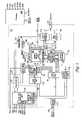
- FIG. 1One embodiment of the present invention is illustrated in FIG. 1 .
- first and second redundant circuits 150 , 152are coupled to an array of non-volatile memory cells 102 in a synchronous flash memory device 100 .
- a synchronous flash memorycombines the non-volatile storage capacities of flash memory with a SDRAM compatible interface.
- this embodimentdeals with a synchronous flash memory, it will be appreciated by those in the art, that the present invention can be applied to other flash memory systems and that the present invention is not limited to synchronous flash memory systems.
- the memory device 100 of this embodimentincludes an array of non-volatile flash memory cells 102 .
- the arrayis arranged in a plurality of addressable banks.
- the memorycontains four memory banks 104 , 106 , 108 and 110 .
- Each memory bankcontains addressable sectors of memory cells.
- Command execution logic 130is provided to control the basic operations of the memory device.
- a state machine 132is also provided to control specific operations performed on the memory array and cells.
- the command execution logic 130 and/or state machine 132can be generally referred to as control circuitry 138 to control read, write and other memory operations. More importantly for the present invention, the state machine 132 or control circuitry 138 controls the erase operation algorithm of the array of non-volatile flash memory cells 102 .
- a status register 134 and an identification register 136can also be provided to output data.
- the data connections (DQ) 143are typically used for bi-directional data communication.
- the memorycan be coupled to an external processor 200 for operation or testing.
- the data stored in the memorycan be accessed using externally provided location addresses received by address register 112 via address signal connections 133 .
- the row addressesare decoded using row address multiplexer circuitry 114 .
- the addressesare also decoded using bank control logic 116 and row address latch and decode circuitry 118 .
- column address counter and latch circuitry 120couples the received addresses to column decode circuitry 122 .
- Circuit 124provides input/output gating, data mask logic, read data latch circuitry and write driver circuitry. Data is input through data input registers 126 and output through data output registers 128 via data connections.
- the synchronous flash memory array architectureis designed to allow blocks of memory cells to be erased without disturbing the rest of the array.
- the arrayis divided into 16 addressable blocks that are independently erasable. By erasing blocks rather than the entire array, the total device endurance is enhanced, as is system flexibility.
- the arrayis equally divided into four banks 104 , 106 , 108 and 110 of four blocks each (16 blocks).
- the four bankshave simultaneous read-while-write functionality. That is, a WRITE or ERASE operation to any bank can occur simultaneously to a READ operation to any other bank.
- FIG. 3A simplified illustration of one embodiment of the first redundant circuit 150 and the second redundant circuit 152 is illustrated in FIG. 3 .
- the first redundant circuit 150 and the second redundant circuit 152are coupled to a primary array 154 .
- the respective first or second redundant circuit 150 , 152compares the requested address to the addresses stored in the registers, if a match is found the respective redundant row or column is pointed to instead of a defected row or column in the primary array 154 .
- FIG. 3illustrates a first and second redundant circuit 150 , 152 , it will be realized by those in the art that the first and second redundant circuit 150 , 152 could be combined into one circuit and that the present invention is not limited to a first and second redundant circuit 150 , 152 .
- the reference to a redundant circuit 156 used in this descriptionshall mean a first and second redundant circuit 150 , 152 .
- FIG. 4A simplified illustration of how the redundant row and columns are mapped or coupled to the primary array is illustrated in FIG. 4 .
- FIG. 4is illustrated with a primary array 154 of rows or word lines WL 0 through WLN and columns or bit lines BL 0 through BLN.
- the rows and columns in the primary array 154are coupled to redundant rows BLR 0 through BLN and redundant columns WLR 0 through WLRN.
- the first or second redundant circuit 150 , 152redirects the address request from the defective row or column to an associated redundant row or column. For example, if row WL 0 is found to be defective the second redundant circuit 152 redirects an address request directed to word line WL 0 to redundant word line WLR 0 . Likewise, if column BL 0 is found to be defective the first redundant circuit 150 redirects an address request directed to column BL 0 to redundant column BLR 0 .
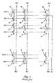
- FIG. 5A redundant circuit 156 and a register 40 of one embodiment of the present invention is illustrated in FIG. 5 .
- the register 40stores an address of an associated defective element in the primary array 154 .
- the register 40also has at least one extra memory cell or bit to store an error code.
- the error codedesignates the type of defect in the defective element. That is, the error code describes the defect in the element in the primary array that is corrected by the redundant element.
- FIG. 5illustrates four registers 40 each having 2-bits of error code.
- the number of registers 40 usedwill depend on the number of redundant elements used to repair defective elements in a primary memory array and the present invention is not limited to four registers.
- the number of bits used to store the error code in each registerwill depend on the number of different types of errors tracked in the defective elements and the present invention is not limited to registers with two bits to store error codes.
- a redundant circuit 156determines an address request matches an address in a register 40 , the redundant circuit 156 relays the error code from the register 40 to the state machine 132 or control circuitry 138 .
- the state machine 132executes an erase operation algorithm that is specific to each error code. For example, an error code could indicate an isolated defected, a row to Column short or a row-to-row short. The state machine 132 would then implement an erase operation algorithm to specifically deal with an isolated defect, a row to column short or a row-to-row short.
- a typical erase operationis implemented on a block of memory cells 30 until an address is discovered that matches an address in a register 40 .
- the error code in the register 40is then read and the appropriate erase operation is applied. If the error code indicates an isolated defect, a typical erase operation is continued. If the error code indicates a row to column short, a row to column erase operation is performed. In addition, if the error code indicates a row-to-row short, a row-to-row erase operation will be performed.
- the algorithm of the present inventiondirects the address decoder to point to the redundant row or column instead of the defective row or column during the pre-program cycle.
- the redundant row or columnis then pre-programmed. Once the redundant row or column is pre-programmed, the address in the next row or column of the primary array is selected and pre-programmed.
- the pre-program cyclecontinues until all addresses of the primary array have been accessed. An erase cycle is then performed. A typical erase cycle is performed in the same manner as previously described.
- the over-erase check operationbegins by monitoring the current levels in each column for a current that would indicate an over-erased cell is coupled to the bit line BL. If a current level is discovered that indicates an over-erase cell coupled to a column or bit line BL, a soft program pulse is applied to each row or word line WL until the current level indicating an over-erased cell is no longer detected. When an address matches an address in a register 40 , a soft program pulse is applied to the redundant elements associated to the register 40 instead of the defective elements.
- An example of an isolated defectwould be a bad memory cell, a broken word line WL or a broken bit line BL.
- the pre-program cyclestarts by pre-programming the redundant rows and columns. Once the redundant rows and columns have been pre-programmed, the pre-program cycle is performed on the primary array 154 . The pre-program cycle is performed incrementally until an address of a row or column matches the address in a register associated with a redundant row or column. The algorithm then disables the redundant circuit 156 (the respective first or second redundant circuit 150 , 152 ) and pre-programs the memory cells in the row or column in the primary array 154 . An erase cycle is then performed. An erase cycle in a row to column erase operation is performed in the same manner as previously described.
- the soft programming cycleis performed. If a current level is detected in a bit line BL or column that would indicate an over-erased cell is coupled to the column, a soft program pulse is applied to the word lines WL or rows coupled to the suspect column starting with the redundant rows and then proceeding incrementally through the rows of the primary array. After a soft program pulse is applied to a row, the bit line is checked for current. If the current level indicates an over-erased cell is no longer detected, it is assumed that the depleted cell was recovered and the state machine moves on to the next bit line BL. If the current level still indicates an over-erased cell is coupled to the column, a soft program pulse is applied to the following row.
- the algorithmdisables the redundant circuit and applies a soft program pulse to the row in the primary array. If a current level that would indicate an over-erased cell is no longer detected in the bit line after the soft program pulse, the state machine moves on to the next column. If, however, the current level still indicates that an over-erased cell is coupled to the column, the state machine applies a soft program pulse to the next row and so forth until the current level indicates an over-erased cell is no longer detected in the column.
- the algorithmdisables the redundant matching circuitry and applies the soft program pulses to the memory cells coupled to the column.
- the state machineproceeds through the remaining columns.
- the pre-program cycle of a row-to-row erase operationbegins with pre-programming the redundant memory elements in the redundant memory rows. Thereafter, the memory cells in each block of the memory array are pre-programmed incrementally by row and column addresses. If the redundant circuit comes upon a row address that matches an address in a register 40 and the error code in the register indicates a row-to-row short, the redundant circuit is disabled. The algorithm in the state machine then instructs the decoder to select the current row (row S) and the next row (row S+1) at the same time. The algorithm assumes that row S is shorted to row S+1. Row S and row S+1 are activated together and then programmed simultaneously.
- the algorithmcauses the address counter to jump forward a row, thereby skipping over S+1. This process is continued with the rest of the rows until all the memory cells 30 in the block of memory are programmed.
- An erase cycleis performed once the pre-program cycle has been completed.
- An erase cycle in a row to column erase operationis performed in the same manner as previously described.
- the soft programming cyclebegins.
- the algorithmdirects the state machine to check each bit line for a current level, with all the word lines off, that would indicate an over-erased cell is coupled to the column.
- the state machinestarts with the first column or bit line BL and proceeds incrementally. If current level is detected above the threshold value in column, a soft program pulse is applied to the rows coupled to the suspect column starting with the redundant rows and then proceeding incrementally through the rows of the primary array 154 . After a soft program pulse is applied to a row, the current level in the bit line is once again checked. If the current level indicates an over-erased cell is no longer detected, it is assumed that the depleted cell was recovered and the state machine moves on to the next bit line BL. If the current level still indicates an over-erased cell is coupled to the column, the soft program is applied to the next row.
- the algorithmdisables the redundant matching circuitry and activates row S and row S+1.
- a soft program pulseis then applied to the cells at row S and row S+1 simultaneously. If the current level no longer indicates an over-erased cell is coupled to the column after row S and row S+1 are simultaneously applied a soft program pulse, the state machine moves on to the next column. If, however, the current level still indicates an over-erased cell is coupled to the column, the state machine increments the row address to skip over S+1 and applies soft program pulse to the next row. The state machine will then proceed through all the remaining rows in the effected column until a current level that indicates an over-erased memory cell is no longer detected.
- a memory device to perform an erase operation algorithm that specifically deals with different types of defects in a memory arrayhas been described.
- the memory array of one embodiment of the present inventionhas primary and redundant elements.
- a registeris used for each redundant element to store the address of a defective primary element and an error code that indicates the type of defect in the defective primary element.
- Control circuitryis used to control memory operations to the memory array. The control circuitry performs an erase operation algorithm that is specific to an error code when a defective primary element is addressed during an erase operation.
Landscapes
- For Increasing The Reliability Of Semiconductor Memories (AREA)
- Read Only Memory (AREA)
Abstract
Description
Claims (17)
Priority Applications (1)
| Application Number | Priority Date | Filing Date | Title |
|---|---|---|---|
| US10/932,496US7168013B2 (en) | 2001-04-19 | 2004-09-02 | Memory with element redundancy |
Applications Claiming Priority (2)
| Application Number | Priority Date | Filing Date | Title |
|---|---|---|---|
| US09/838,764US7162668B2 (en) | 2001-04-19 | 2001-04-19 | Memory with element redundancy |
| US10/932,496US7168013B2 (en) | 2001-04-19 | 2004-09-02 | Memory with element redundancy |
Related Parent Applications (1)
| Application Number | Title | Priority Date | Filing Date |
|---|---|---|---|
| US09/838,764DivisionUS7162668B2 (en) | 2001-04-09 | 2001-04-19 | Memory with element redundancy |
Publications (2)
| Publication Number | Publication Date |
|---|---|
| US20050024982A1 US20050024982A1 (en) | 2005-02-03 |
| US7168013B2true US7168013B2 (en) | 2007-01-23 |
Family
ID=25277989
Family Applications (4)
| Application Number | Title | Priority Date | Filing Date |
|---|---|---|---|
| US09/838,764Expired - LifetimeUS7162668B2 (en) | 2001-04-09 | 2001-04-19 | Memory with element redundancy |
| US10/932,968Expired - Fee RelatedUS7047455B2 (en) | 2001-04-09 | 2004-09-02 | Memory with element redundancy |
| US10/932,948Expired - LifetimeUS7076702B2 (en) | 2001-04-09 | 2004-09-02 | Memory with element redundancy |
| US10/932,496Expired - LifetimeUS7168013B2 (en) | 2001-04-19 | 2004-09-02 | Memory with element redundancy |
Family Applications Before (3)
| Application Number | Title | Priority Date | Filing Date |
|---|---|---|---|
| US09/838,764Expired - LifetimeUS7162668B2 (en) | 2001-04-09 | 2001-04-19 | Memory with element redundancy |
| US10/932,968Expired - Fee RelatedUS7047455B2 (en) | 2001-04-09 | 2004-09-02 | Memory with element redundancy |
| US10/932,948Expired - LifetimeUS7076702B2 (en) | 2001-04-09 | 2004-09-02 | Memory with element redundancy |
Country Status (1)
| Country | Link |
|---|---|
| US (4) | US7162668B2 (en) |
Cited By (4)
| Publication number | Priority date | Publication date | Assignee | Title |
|---|---|---|---|---|
| US20060107130A1 (en)* | 2004-11-04 | 2006-05-18 | Sigmatel, Inc. | System and method of reading non-volatile computer memory |
| US20100080074A1 (en)* | 2008-09-30 | 2010-04-01 | Semiconductor Energy Laboratory Co., Ltd. | Semiconductor memory device |
| US20110058415A1 (en)* | 2009-09-08 | 2011-03-10 | Lsi Corporation | Systems and Methods for Increasing Bit Density in a Memory Cell |
| US8937845B2 (en) | 2012-10-31 | 2015-01-20 | Freescale Semiconductor, Inc. | Memory device redundancy management system |
Families Citing this family (30)
| Publication number | Priority date | Publication date | Assignee | Title |
|---|---|---|---|---|
| US6711056B2 (en) | 2001-03-12 | 2004-03-23 | Micron Technology, Inc. | Memory with row redundancy |
| US6865702B2 (en)* | 2001-04-09 | 2005-03-08 | Micron Technology, Inc. | Synchronous flash memory with test code input |
| US20030051193A1 (en)* | 2001-09-10 | 2003-03-13 | Dell Products L.P. | Computer system with improved error detection |
| JP4028301B2 (en)* | 2002-06-11 | 2007-12-26 | 富士通株式会社 | Nonvolatile semiconductor memory device and erase method thereof |
| US7123512B2 (en)* | 2002-07-19 | 2006-10-17 | Micron Technology, Inc. | Contiguous block addressing scheme |
| US6941411B2 (en) | 2002-08-21 | 2005-09-06 | Micron Technology, Inc. | Non-contiguous address erasable blocks and command in flash memory |
| TW578160B (en)* | 2002-11-29 | 2004-03-01 | Via Tech Inc | Memory modeling circuit with fault tolerant |
| US6771545B1 (en)* | 2003-01-29 | 2004-08-03 | Advanced Micro Devices Inc. | Method for reading a non-volatile memory cell adjacent to an inactive region of a non-volatile memory cell array |
| DE10334520B4 (en)* | 2003-07-29 | 2008-08-21 | Infineon Technologies Ag | Method and device for error correction in a digital memory |
| US7053647B2 (en)* | 2004-05-07 | 2006-05-30 | Taiwan Semiconductor Manufacturing Co., Ltd. | Method of detecting potential bridging effects between conducting lines in an integrated circuit |
| US7630258B2 (en)* | 2004-09-30 | 2009-12-08 | Texas Instruments Incorporated | Decoder based set associative repair cache systems and methods |
| US7275190B2 (en) | 2004-11-08 | 2007-09-25 | Micron Technology, Inc. | Memory block quality identification in a memory device |
| US7761773B2 (en)* | 2005-06-30 | 2010-07-20 | Sigmatel, Inc. | Semiconductor device including a unique identifier and error correction code |
| US7551498B2 (en)* | 2006-12-15 | 2009-06-23 | Atmel Corporation | Implementation of column redundancy for a flash memory with a high write parallelism |
| US9373362B2 (en)* | 2007-08-14 | 2016-06-21 | Dell Products L.P. | System and method for implementing a memory defect map |
| US7945815B2 (en) | 2007-08-14 | 2011-05-17 | Dell Products L.P. | System and method for managing memory errors in an information handling system |
| US7694195B2 (en) | 2007-08-14 | 2010-04-06 | Dell Products L.P. | System and method for using a memory mapping function to map memory defects |
| US7949913B2 (en)* | 2007-08-14 | 2011-05-24 | Dell Products L.P. | Method for creating a memory defect map and optimizing performance using the memory defect map |
| US8321726B2 (en)* | 2008-06-18 | 2012-11-27 | Arm Limited | Repairing memory arrays |
| TWI482168B (en)* | 2010-10-08 | 2015-04-21 | Macronix Int Co Ltd | Method and apparatus for memory repair with redundant columns |
| TWI459393B (en)* | 2011-01-19 | 2014-11-01 | Phison Electronics Corp | Data writing method for a non-volatile memory module, memory controller and memory storage apparatus |
| US8724408B2 (en) | 2011-11-29 | 2014-05-13 | Kingtiger Technology (Canada) Inc. | Systems and methods for testing and assembling memory modules |
| US9117552B2 (en) | 2012-08-28 | 2015-08-25 | Kingtiger Technology(Canada), Inc. | Systems and methods for testing memory |
| US8971137B2 (en)* | 2013-03-07 | 2015-03-03 | Intel Corporation | Bit based fuse repair |
| JP5657079B1 (en)* | 2013-10-24 | 2015-01-21 | ウィンボンド エレクトロニクス コーポレーション | Semiconductor memory device |
| US9274888B2 (en)* | 2013-11-15 | 2016-03-01 | Qualcomm Incorporated | Method and apparatus for multiple-bit DRAM error recovery |
| FR3014688B1 (en)* | 2013-12-12 | 2016-12-16 | Laboratoires Inneov S N C | COMPOSITION BASED ON POLYUNSATURATED FATTY ACID AND CAROTENOID FOR ORAL ADMINISTRATION TO ENHANCE THE QUALITY OF THE HAIR |
| CN104900269B (en)* | 2014-03-04 | 2018-01-05 | 华邦电子股份有限公司 | Semiconductor memory device and redundancy method thereof |
| KR102402406B1 (en)* | 2016-03-17 | 2022-05-27 | 에스케이하이닉스 주식회사 | Semiconductor device |
| US10635246B2 (en)* | 2017-03-10 | 2020-04-28 | Cypress Semiconductor Corporation | Capacitance sensing and inductance sensing in different modes |
Citations (29)
| Publication number | Priority date | Publication date | Assignee | Title |
|---|---|---|---|---|
| US4899342A (en) | 1988-02-01 | 1990-02-06 | Thinking Machines Corporation | Method and apparatus for operating multi-unit array of memories |
| US5077736A (en) | 1988-06-28 | 1991-12-31 | Storage Technology Corporation | Disk drive memory |
| US5128944A (en)* | 1989-05-26 | 1992-07-07 | Texas Instruments Incorporated | Apparatus and method for providing notification of bit-cell failure in a redundant-bit-cell memory |
| US5233559A (en)* | 1991-02-11 | 1993-08-03 | Intel Corporation | Row redundancy for flash memories |
| US5243570A (en)* | 1992-01-31 | 1993-09-07 | Nec Corporation | Semiconductor memory device having redundant memory cell columns concurrently accessible together with regular memory cell arrays |
| US5329488A (en) | 1991-12-27 | 1994-07-12 | Nec Corporation | Nonvolatile semiconductor memory device with redundancy circuit |
| US5359569A (en) | 1991-10-29 | 1994-10-25 | Hitachi Ltd. | Semiconductor memory |
| US5377147A (en)* | 1992-04-21 | 1994-12-27 | Intel Corporation | Method and circuitry for preconditioning shorted rows in a nonvolatile semiconductor memory incorporating row redundancy |
| US5392292A (en) | 1991-06-27 | 1995-02-21 | Cray Research, Inc. | Configurable spare memory chips |
| US5428621A (en)* | 1992-09-21 | 1995-06-27 | Sundisk Corporation | Latent defect handling in EEPROM devices |
| US5517634A (en)* | 1992-06-23 | 1996-05-14 | Quantum Corporation | Disk drive system including a DRAM array and associated method for programming initial information into the array |
| US5559742A (en) | 1995-02-23 | 1996-09-24 | Micron Technology, Inc. | Flash memory having transistor redundancy |
| US5602987A (en) | 1989-04-13 | 1997-02-11 | Sandisk Corporation | Flash EEprom system |
| US5671239A (en)* | 1993-09-20 | 1997-09-23 | Fujitsu Limited | Semiconductor memory of xN type having error correcting circuit by parity |
| US5761128A (en)* | 1996-03-28 | 1998-06-02 | Nec Corporation | Non-volatile semiconductor memory device |
| US5774396A (en)* | 1996-03-29 | 1998-06-30 | Aplus Integrated Circuits, Inc. | Flash memory with row redundancy |
| US5796653A (en) | 1994-02-23 | 1998-08-18 | Sgs-Thomson Microelectronics, S.A. | Circuit for the selection of redundant memory elements and flash EEPROM memory comprising said circuit |
| US5883903A (en)* | 1993-09-20 | 1999-03-16 | Fujitsu Limited | Semiconductor memory of XN type having parity corresponding to n×m bits |
| US5917838A (en) | 1998-01-05 | 1999-06-29 | General Dynamics Information Systems, Inc. | Fault tolerant memory system |
| US5920508A (en)* | 1997-02-26 | 1999-07-06 | Kabushiki Kaisha Toshiba | Semiconductor memory device |
| US5995413A (en) | 1998-01-09 | 1999-11-30 | Information Storage Devices, Inc. | Trimbit circuit for flash memory integrated circuits |
| US6034891A (en) | 1997-12-01 | 2000-03-07 | Micron Technology, Inc. | Multi-state flash memory defect management |
| US6078534A (en) | 1997-09-25 | 2000-06-20 | Siemens Aktiengesellschaft | Semiconductor memory having redundancy circuit |
| US6108250A (en)* | 1999-04-15 | 2000-08-22 | Alliance Semiconductor Corporation | Fast redundancy scheme for high density, high speed memories |
| US6351412B1 (en) | 1999-04-26 | 2002-02-26 | Hitachi, Ltd. | Memory card |
| US6469932B2 (en)* | 2001-03-12 | 2002-10-22 | Micron Technology, Inc. | Memory with row redundancy |
| US6505306B1 (en) | 1999-09-15 | 2003-01-07 | International Business Machines Corporation | Redundant bit steering mechanism with delayed switchover of fetch operations during redundant device initialization |
| US6711056B2 (en)* | 2001-03-12 | 2004-03-23 | Micron Technology, Inc. | Memory with row redundancy |
| US6771541B1 (en)* | 2003-02-25 | 2004-08-03 | Nexflash Technologies, Inc. | Method and apparatus for providing row redundancy in nonvolatile semiconductor memory |
Family Cites Families (8)
| Publication number | Priority date | Publication date | Assignee | Title |
|---|---|---|---|---|
| JPH0498342A (en)* | 1990-08-09 | 1992-03-31 | Mitsubishi Electric Corp | semiconductor storage device |
| US5550394A (en)* | 1993-06-18 | 1996-08-27 | Texas Instruments Incorporated | Semiconductor memory device and defective memory cell correction circuit |
| US5329569A (en)* | 1993-02-18 | 1994-07-12 | Sandia Corporation | X-ray transmissive debris shield |
| JP3249871B2 (en)* | 1993-12-22 | 2002-01-21 | 三菱電機株式会社 | Semiconductor storage device |
| JPH1011993A (en)* | 1996-06-27 | 1998-01-16 | Mitsubishi Electric Corp | Semiconductor storage device |
| US6496425B1 (en)* | 2000-08-21 | 2002-12-17 | Micron Technology, Inc | Multiple bit line column redundancy |
| US6333882B1 (en)* | 2000-08-25 | 2001-12-25 | Micron Technology, Inc. | Equilibration/pre-charge circuit for a memory device |
| US6816420B1 (en)* | 2003-07-29 | 2004-11-09 | Xilinx, Inc. | Column redundancy scheme for serially programmable integrated circuits |
- 2001
- 2001-04-19USUS09/838,764patent/US7162668B2/ennot_activeExpired - Lifetime
- 2004
- 2004-09-02USUS10/932,968patent/US7047455B2/ennot_activeExpired - Fee Related
- 2004-09-02USUS10/932,948patent/US7076702B2/ennot_activeExpired - Lifetime
- 2004-09-02USUS10/932,496patent/US7168013B2/ennot_activeExpired - Lifetime
Patent Citations (32)
| Publication number | Priority date | Publication date | Assignee | Title |
|---|---|---|---|---|
| US4899342A (en) | 1988-02-01 | 1990-02-06 | Thinking Machines Corporation | Method and apparatus for operating multi-unit array of memories |
| US5077736A (en) | 1988-06-28 | 1991-12-31 | Storage Technology Corporation | Disk drive memory |
| US6149316A (en) | 1989-04-13 | 2000-11-21 | Sandisk Corporation | Flash EEprom system |
| US5602987A (en) | 1989-04-13 | 1997-02-11 | Sandisk Corporation | Flash EEprom system |
| US5128944A (en)* | 1989-05-26 | 1992-07-07 | Texas Instruments Incorporated | Apparatus and method for providing notification of bit-cell failure in a redundant-bit-cell memory |
| US5233559A (en)* | 1991-02-11 | 1993-08-03 | Intel Corporation | Row redundancy for flash memories |
| US5392292A (en) | 1991-06-27 | 1995-02-21 | Cray Research, Inc. | Configurable spare memory chips |
| US5359569A (en) | 1991-10-29 | 1994-10-25 | Hitachi Ltd. | Semiconductor memory |
| US5329488A (en) | 1991-12-27 | 1994-07-12 | Nec Corporation | Nonvolatile semiconductor memory device with redundancy circuit |
| US5243570A (en)* | 1992-01-31 | 1993-09-07 | Nec Corporation | Semiconductor memory device having redundant memory cell columns concurrently accessible together with regular memory cell arrays |
| US5377147A (en)* | 1992-04-21 | 1994-12-27 | Intel Corporation | Method and circuitry for preconditioning shorted rows in a nonvolatile semiconductor memory incorporating row redundancy |
| US5517634A (en)* | 1992-06-23 | 1996-05-14 | Quantum Corporation | Disk drive system including a DRAM array and associated method for programming initial information into the array |
| US5428621A (en)* | 1992-09-21 | 1995-06-27 | Sundisk Corporation | Latent defect handling in EEPROM devices |
| US5671239A (en)* | 1993-09-20 | 1997-09-23 | Fujitsu Limited | Semiconductor memory of xN type having error correcting circuit by parity |
| US5883903A (en)* | 1993-09-20 | 1999-03-16 | Fujitsu Limited | Semiconductor memory of XN type having parity corresponding to n×m bits |
| US5796653A (en) | 1994-02-23 | 1998-08-18 | Sgs-Thomson Microelectronics, S.A. | Circuit for the selection of redundant memory elements and flash EEPROM memory comprising said circuit |
| US5559742A (en) | 1995-02-23 | 1996-09-24 | Micron Technology, Inc. | Flash memory having transistor redundancy |
| US5748527A (en)* | 1995-02-23 | 1998-05-05 | Micron Technology, Inc. | Nonvolatile memory having transistor redundancy |
| US5761128A (en)* | 1996-03-28 | 1998-06-02 | Nec Corporation | Non-volatile semiconductor memory device |
| US5774396A (en)* | 1996-03-29 | 1998-06-30 | Aplus Integrated Circuits, Inc. | Flash memory with row redundancy |
| US5920508A (en)* | 1997-02-26 | 1999-07-06 | Kabushiki Kaisha Toshiba | Semiconductor memory device |
| US6078534A (en) | 1997-09-25 | 2000-06-20 | Siemens Aktiengesellschaft | Semiconductor memory having redundancy circuit |
| US6034891A (en) | 1997-12-01 | 2000-03-07 | Micron Technology, Inc. | Multi-state flash memory defect management |
| US5917838A (en) | 1998-01-05 | 1999-06-29 | General Dynamics Information Systems, Inc. | Fault tolerant memory system |
| US5995413A (en) | 1998-01-09 | 1999-11-30 | Information Storage Devices, Inc. | Trimbit circuit for flash memory integrated circuits |
| US6108250A (en)* | 1999-04-15 | 2000-08-22 | Alliance Semiconductor Corporation | Fast redundancy scheme for high density, high speed memories |
| US6351412B1 (en) | 1999-04-26 | 2002-02-26 | Hitachi, Ltd. | Memory card |
| US6359806B1 (en) | 1999-04-26 | 2002-03-19 | Hitachi, Ltd. | Memory device |
| US6505306B1 (en) | 1999-09-15 | 2003-01-07 | International Business Machines Corporation | Redundant bit steering mechanism with delayed switchover of fetch operations during redundant device initialization |
| US6469932B2 (en)* | 2001-03-12 | 2002-10-22 | Micron Technology, Inc. | Memory with row redundancy |
| US6711056B2 (en)* | 2001-03-12 | 2004-03-23 | Micron Technology, Inc. | Memory with row redundancy |
| US6771541B1 (en)* | 2003-02-25 | 2004-08-03 | Nexflash Technologies, Inc. | Method and apparatus for providing row redundancy in nonvolatile semiconductor memory |
Cited By (6)
| Publication number | Priority date | Publication date | Assignee | Title |
|---|---|---|---|---|
| US20060107130A1 (en)* | 2004-11-04 | 2006-05-18 | Sigmatel, Inc. | System and method of reading non-volatile computer memory |
| US7409623B2 (en)* | 2004-11-04 | 2008-08-05 | Sigmatel, Inc. | System and method of reading non-volatile computer memory |
| US20100080074A1 (en)* | 2008-09-30 | 2010-04-01 | Semiconductor Energy Laboratory Co., Ltd. | Semiconductor memory device |
| US20110058415A1 (en)* | 2009-09-08 | 2011-03-10 | Lsi Corporation | Systems and Methods for Increasing Bit Density in a Memory Cell |
| US8243536B2 (en)* | 2009-09-08 | 2012-08-14 | Lsi Corporation | Systems and methods for increasing bit density in a memory cell |
| US8937845B2 (en) | 2012-10-31 | 2015-01-20 | Freescale Semiconductor, Inc. | Memory device redundancy management system |
Also Published As
| Publication number | Publication date |
|---|---|
| US7162668B2 (en) | 2007-01-09 |
| US20050024982A1 (en) | 2005-02-03 |
| US7047455B2 (en) | 2006-05-16 |
| US20050028054A1 (en) | 2005-02-03 |
| US20050028053A1 (en) | 2005-02-03 |
| US7076702B2 (en) | 2006-07-11 |
| US20020157048A1 (en) | 2002-10-24 |
Similar Documents
| Publication | Publication Date | Title |
|---|---|---|
| US7168013B2 (en) | Memory with element redundancy | |
| US6553510B1 (en) | Memory device including redundancy routine for correcting random errors | |
| US6646930B2 (en) | Non-volatile semiconductor memory | |
| US7437625B2 (en) | Memory with element redundancy | |
| JP3941149B2 (en) | Semiconductor nonvolatile memory device | |
| US6381174B1 (en) | Non-volatile memory device with redundant columns | |
| US7359243B2 (en) | Memory cell repair using fuse programming method in a flash memory device | |
| JP3672435B2 (en) | Nonvolatile memory device | |
| US8023341B2 (en) | Method and apparatus for address allotting and verification in a semiconductor device | |
| KR100315321B1 (en) | Nonvolatile semiconductor memory device and erase verify method therefor | |
| US7336537B2 (en) | Handling defective memory blocks of NAND memory devices | |
| US5590075A (en) | Method for testing an electrically erasable and programmable memory device | |
| KR20100040288A (en) | Programmable chip enable and chip address in semiconductor memory | |
| US6469932B2 (en) | Memory with row redundancy | |
| JP4439539B2 (en) | Nonvolatile semiconductor memory and test method thereof | |
| US6711056B2 (en) | Memory with row redundancy | |
| US7640465B2 (en) | Memory with element redundancy | |
| US7200049B2 (en) | Methods for accelerated erase operations in non-volatile memory devices and related devices | |
| JP2005018983A (en) | Semiconductor nonvolatile memory device and memory system | |
| JP2006004478A (en) | Nonvolatile semiconductor memory device | |
| JP2004039179A (en) | Nonvolatile semiconductor memory device and redundant replacement method for nonvolatile semiconductor memory device |
Legal Events
| Date | Code | Title | Description |
|---|---|---|---|
| FEPP | Fee payment procedure | Free format text:PAYOR NUMBER ASSIGNED (ORIGINAL EVENT CODE: ASPN); ENTITY STATUS OF PATENT OWNER: LARGE ENTITY | |
| STCF | Information on status: patent grant | Free format text:PATENTED CASE | |
| FPAY | Fee payment | Year of fee payment:4 | |
| FPAY | Fee payment | Year of fee payment:8 | |
| AS | Assignment | Owner name:U.S. BANK NATIONAL ASSOCIATION, AS COLLATERAL AGENT, CALIFORNIA Free format text:SECURITY INTEREST;ASSIGNOR:MICRON TECHNOLOGY, INC.;REEL/FRAME:038669/0001 Effective date:20160426 Owner name:U.S. BANK NATIONAL ASSOCIATION, AS COLLATERAL AGEN Free format text:SECURITY INTEREST;ASSIGNOR:MICRON TECHNOLOGY, INC.;REEL/FRAME:038669/0001 Effective date:20160426 | |
| AS | Assignment | Owner name:MORGAN STANLEY SENIOR FUNDING, INC., AS COLLATERAL AGENT, MARYLAND Free format text:PATENT SECURITY AGREEMENT;ASSIGNOR:MICRON TECHNOLOGY, INC.;REEL/FRAME:038954/0001 Effective date:20160426 Owner name:MORGAN STANLEY SENIOR FUNDING, INC., AS COLLATERAL Free format text:PATENT SECURITY AGREEMENT;ASSIGNOR:MICRON TECHNOLOGY, INC.;REEL/FRAME:038954/0001 Effective date:20160426 | |
| AS | Assignment | Owner name:U.S. BANK NATIONAL ASSOCIATION, AS COLLATERAL AGENT, CALIFORNIA Free format text:CORRECTIVE ASSIGNMENT TO CORRECT THE REPLACE ERRONEOUSLY FILED PATENT #7358718 WITH THE CORRECT PATENT #7358178 PREVIOUSLY RECORDED ON REEL 038669 FRAME 0001. ASSIGNOR(S) HEREBY CONFIRMS THE SECURITY INTEREST;ASSIGNOR:MICRON TECHNOLOGY, INC.;REEL/FRAME:043079/0001 Effective date:20160426 Owner name:U.S. BANK NATIONAL ASSOCIATION, AS COLLATERAL AGEN Free format text:CORRECTIVE ASSIGNMENT TO CORRECT THE REPLACE ERRONEOUSLY FILED PATENT #7358718 WITH THE CORRECT PATENT #7358178 PREVIOUSLY RECORDED ON REEL 038669 FRAME 0001. ASSIGNOR(S) HEREBY CONFIRMS THE SECURITY INTEREST;ASSIGNOR:MICRON TECHNOLOGY, INC.;REEL/FRAME:043079/0001 Effective date:20160426 | |
| MAFP | Maintenance fee payment | Free format text:PAYMENT OF MAINTENANCE FEE, 12TH YEAR, LARGE ENTITY (ORIGINAL EVENT CODE: M1553) Year of fee payment:12 | |
| AS | Assignment | Owner name:JPMORGAN CHASE BANK, N.A., AS COLLATERAL AGENT, ILLINOIS Free format text:SECURITY INTEREST;ASSIGNORS:MICRON TECHNOLOGY, INC.;MICRON SEMICONDUCTOR PRODUCTS, INC.;REEL/FRAME:047540/0001 Effective date:20180703 Owner name:JPMORGAN CHASE BANK, N.A., AS COLLATERAL AGENT, IL Free format text:SECURITY INTEREST;ASSIGNORS:MICRON TECHNOLOGY, INC.;MICRON SEMICONDUCTOR PRODUCTS, INC.;REEL/FRAME:047540/0001 Effective date:20180703 | |
| AS | Assignment | Owner name:MICRON TECHNOLOGY, INC., IDAHO Free format text:RELEASE BY SECURED PARTY;ASSIGNOR:U.S. BANK NATIONAL ASSOCIATION, AS COLLATERAL AGENT;REEL/FRAME:047243/0001 Effective date:20180629 | |
| AS | Assignment | Owner name:MICRON TECHNOLOGY, INC., IDAHO Free format text:RELEASE BY SECURED PARTY;ASSIGNOR:MORGAN STANLEY SENIOR FUNDING, INC., AS COLLATERAL AGENT;REEL/FRAME:050937/0001 Effective date:20190731 | |
| AS | Assignment | Owner name:MICRON TECHNOLOGY, INC., IDAHO Free format text:RELEASE BY SECURED PARTY;ASSIGNOR:JPMORGAN CHASE BANK, N.A., AS COLLATERAL AGENT;REEL/FRAME:051028/0001 Effective date:20190731 Owner name:MICRON SEMICONDUCTOR PRODUCTS, INC., IDAHO Free format text:RELEASE BY SECURED PARTY;ASSIGNOR:JPMORGAN CHASE BANK, N.A., AS COLLATERAL AGENT;REEL/FRAME:051028/0001 Effective date:20190731 |