US7166524B2 - Method for ion implanting insulator material to reduce dielectric constant - Google Patents
Method for ion implanting insulator material to reduce dielectric constantDownload PDFInfo
- Publication number
- US7166524B2 US7166524B2US11/003,000US300004AUS7166524B2US 7166524 B2US7166524 B2US 7166524B2US 300004 AUS300004 AUS 300004AUS 7166524 B2US7166524 B2US 7166524B2
- Authority
- US
- United States
- Prior art keywords
- species
- dielectric
- layer
- dielectric layer
- film
- Prior art date
- Legal status (The legal status is an assumption and is not a legal conclusion. Google has not performed a legal analysis and makes no representation as to the accuracy of the status listed.)
- Expired - Fee Related, expires
Links
- 238000000034methodMethods0.000titleclaimsdescription113
- 239000000463materialSubstances0.000titleabstractdescription65
- 239000012212insulatorSubstances0.000titledescription35
- 238000005468ion implantationMethods0.000claimsabstractdescription104
- 239000003989dielectric materialSubstances0.000claimsabstractdescription38
- 239000007789gasSubstances0.000claimsdescription137
- 150000002500ionsChemical class0.000claimsdescription104
- 230000008569processEffects0.000claimsdescription67
- 239000007943implantSubstances0.000claimsdescription31
- 239000011148porous materialSubstances0.000claimsdescription31
- 239000004065semiconductorSubstances0.000claimsdescription27
- 229910052734heliumInorganic materials0.000claimsdescription26
- SWQJXJOGLNCZEY-UHFFFAOYSA-Nhelium atomChemical compound[He]SWQJXJOGLNCZEY-UHFFFAOYSA-N0.000claimsdescription25
- 125000004429atomChemical group0.000claimsdescription24
- 239000001307heliumSubstances0.000claimsdescription22
- 238000000151depositionMethods0.000claimsdescription21
- 238000002513implantationMethods0.000claimsdescription21
- 229910052739hydrogenInorganic materials0.000claimsdescription17
- 239000001257hydrogenSubstances0.000claimsdescription16
- ZOXJGFHDIHLPTG-UHFFFAOYSA-NBoronChemical compound[B]ZOXJGFHDIHLPTG-UHFFFAOYSA-N0.000claimsdescription15
- 229910052796boronInorganic materials0.000claimsdescription15
- 238000007654immersionMethods0.000claimsdescription15
- 230000001105regulatory effectEffects0.000claimsdescription15
- IJGRMHOSHXDMSA-UHFFFAOYSA-NAtomic nitrogenChemical compoundN#NIJGRMHOSHXDMSA-UHFFFAOYSA-N0.000claimsdescription14
- 229910052760oxygenInorganic materials0.000claimsdescription14
- 239000001301oxygenSubstances0.000claimsdescription14
- OAICVXFJPJFONN-UHFFFAOYSA-NPhosphorusChemical compound[P]OAICVXFJPJFONN-UHFFFAOYSA-N0.000claimsdescription13
- QVGXLLKOCUKJST-UHFFFAOYSA-Natomic oxygenChemical compound[O]QVGXLLKOCUKJST-UHFFFAOYSA-N0.000claimsdescription13
- 230000008021depositionEffects0.000claimsdescription13
- 239000011574phosphorusSubstances0.000claimsdescription13
- 229910052698phosphorusInorganic materials0.000claimsdescription13
- OKTJSMMVPCPJKN-UHFFFAOYSA-NCarbonChemical compound[C]OKTJSMMVPCPJKN-UHFFFAOYSA-N0.000claimsdescription11
- 229910052799carbonInorganic materials0.000claimsdescription11
- BLRPTPMANUNPDV-UHFFFAOYSA-NSilaneChemical compound[SiH4]BLRPTPMANUNPDV-UHFFFAOYSA-N0.000claimsdescription10
- 239000002243precursorSubstances0.000claimsdescription10
- 229910000077silaneInorganic materials0.000claimsdescription10
- XKRFYHLGVUSROY-UHFFFAOYSA-NArgonChemical compound[Ar]XKRFYHLGVUSROY-UHFFFAOYSA-N0.000claimsdescription8
- 229910052757nitrogenInorganic materials0.000claimsdescription7
- 229910052786argonInorganic materials0.000claimsdescription6
- 229910052724xenonInorganic materials0.000claimsdescription6
- 229910052785arsenicInorganic materials0.000claimsdescription5
- RQNWIZPPADIBDY-UHFFFAOYSA-Narsenic atomChemical compound[As]RQNWIZPPADIBDY-UHFFFAOYSA-N0.000claimsdescription5
- 230000002708enhancing effectEffects0.000claimsdescription5
- 229910052732germaniumInorganic materials0.000claimsdescription5
- GNPVGFCGXDBREM-UHFFFAOYSA-Ngermanium atomChemical compound[Ge]GNPVGFCGXDBREM-UHFFFAOYSA-N0.000claimsdescription5
- 239000000615nonconductorSubstances0.000claimsdescription5
- FHNFHKCVQCLJFQ-UHFFFAOYSA-Nxenon atomChemical compound[Xe]FHNFHKCVQCLJFQ-UHFFFAOYSA-N0.000claimsdescription5
- 230000008878couplingEffects0.000claimsdescription4
- 238000010168coupling processMethods0.000claimsdescription4
- 238000005859coupling reactionMethods0.000claimsdescription4
- 230000003247decreasing effectEffects0.000claimsdescription4
- 239000000203mixtureSubstances0.000claimsdescription4
- 229910001423beryllium ionInorganic materials0.000claimsdescription3
- 229910052743kryptonInorganic materials0.000claimsdescription3
- DNNSSWSSYDEUBZ-UHFFFAOYSA-Nkrypton atomChemical compound[Kr]DNNSSWSSYDEUBZ-UHFFFAOYSA-N0.000claimsdescription3
- 229910052754neonInorganic materials0.000claimsdescription3
- GKAOGPIIYCISHV-UHFFFAOYSA-Nneon atomChemical compound[Ne]GKAOGPIIYCISHV-UHFFFAOYSA-N0.000claimsdescription3
- WKBOTKDWSSQWDR-UHFFFAOYSA-NBromine atomChemical compound[Br]WKBOTKDWSSQWDR-UHFFFAOYSA-N0.000claimsdescription2
- ZAMOUSCENKQFHK-UHFFFAOYSA-NChlorine atomChemical compound[Cl]ZAMOUSCENKQFHK-UHFFFAOYSA-N0.000claimsdescription2
- PXGOKWXKJXAPGV-UHFFFAOYSA-NFluorineChemical compoundFFPXGOKWXKJXAPGV-UHFFFAOYSA-N0.000claimsdescription2
- 229910004014SiF4Inorganic materials0.000claimsdescription2
- GDTBXPJZTBHREO-UHFFFAOYSA-NbromineSubstancesBrBrGDTBXPJZTBHREO-UHFFFAOYSA-N0.000claimsdescription2
- 229910052794bromiumInorganic materials0.000claimsdescription2
- 239000000460chlorineSubstances0.000claimsdescription2
- 229910052801chlorineInorganic materials0.000claimsdescription2
- 229910052731fluorineInorganic materials0.000claimsdescription2
- 239000011737fluorineSubstances0.000claimsdescription2
- PNDPGZBMCMUPRI-UHFFFAOYSA-NiodineChemical compoundIIPNDPGZBMCMUPRI-UHFFFAOYSA-N0.000claimsdescription2
- ABTOQLMXBSRXSM-UHFFFAOYSA-Nsilicon tetrafluorideChemical compoundF[Si](F)(F)FABTOQLMXBSRXSM-UHFFFAOYSA-N0.000claimsdescription2
- 239000010408filmSubstances0.000claims35
- 125000004435hydrogen atomChemical class[H]*0.000claims1
- 239000010409thin filmSubstances0.000claims1
- 229910052751metalInorganic materials0.000abstractdescription8
- 239000002184metalSubstances0.000abstractdescription8
- 238000004377microelectronicMethods0.000abstractdescription2
- VYPSYNLAJGMNEJ-UHFFFAOYSA-NSilicium dioxideChemical compoundO=[Si]=OVYPSYNLAJGMNEJ-UHFFFAOYSA-N0.000description98
- 235000012239silicon dioxideNutrition0.000description49
- 239000000377silicon dioxideSubstances0.000description49
- 238000009413insulationMethods0.000description40
- NJPPVKZQTLUDBO-UHFFFAOYSA-NnovaluronChemical compoundC1=C(Cl)C(OC(F)(F)C(OC(F)(F)F)F)=CC=C1NC(=O)NC(=O)C1=C(F)C=CC=C1FNJPPVKZQTLUDBO-UHFFFAOYSA-N0.000description16
- 239000011810insulating materialSubstances0.000description14
- 230000015572biosynthetic processEffects0.000description13
- 239000000126substanceSubstances0.000description12
- 239000004020conductorSubstances0.000description11
- UFHFLCQGNIYNRP-UHFFFAOYSA-NHydrogenChemical compound[H][H]UFHFLCQGNIYNRP-UHFFFAOYSA-N0.000description10
- XUIMIQQOPSSXEZ-UHFFFAOYSA-NSiliconChemical compound[Si]XUIMIQQOPSSXEZ-UHFFFAOYSA-N0.000description9
- 238000005498polishingMethods0.000description9
- 230000009467reductionEffects0.000description9
- RYGMFSIKBFXOCR-UHFFFAOYSA-NCopperChemical compound[Cu]RYGMFSIKBFXOCR-UHFFFAOYSA-N0.000description8
- 239000012774insulation materialSubstances0.000description8
- 229910052710siliconInorganic materials0.000description8
- 229910052802copperInorganic materials0.000description7
- 239000010949copperSubstances0.000description7
- 230000004888barrier functionEffects0.000description6
- 230000007423decreaseEffects0.000description6
- 238000000280densificationMethods0.000description6
- 238000010586diagramMethods0.000description6
- 230000006872improvementEffects0.000description6
- 239000011159matrix materialSubstances0.000description6
- 239000010703siliconSubstances0.000description6
- 229910021341titanium silicideInorganic materials0.000description6
- 229910052581Si3N4Inorganic materials0.000description5
- 239000010432diamondSubstances0.000description5
- 238000009826distributionMethods0.000description5
- 230000004907fluxEffects0.000description5
- 150000002431hydrogenChemical class0.000description5
- HQVNEWCFYHHQES-UHFFFAOYSA-Nsilicon nitrideChemical compoundN12[Si]34N5[Si]62N3[Si]51N64HQVNEWCFYHHQES-UHFFFAOYSA-N0.000description5
- 238000000137annealingMethods0.000description4
- 230000032798delaminationEffects0.000description4
- 230000005012migrationEffects0.000description4
- 238000013508migrationMethods0.000description4
- 239000005368silicate glassSubstances0.000description4
- 239000000758substrateSubstances0.000description4
- 230000001276controlling effectEffects0.000description3
- 238000013461designMethods0.000description3
- 238000011049fillingMethods0.000description3
- 125000004430oxygen atomChemical groupO*0.000description3
- ATJFFYVFTNAWJD-UHFFFAOYSA-NTinChemical compound[Sn]ATJFFYVFTNAWJD-UHFFFAOYSA-N0.000description2
- 238000013459approachMethods0.000description2
- 239000010941cobaltSubstances0.000description2
- 229910017052cobaltInorganic materials0.000description2
- GUTLYIVDDKVIGB-UHFFFAOYSA-Ncobalt atomChemical compound[Co]GUTLYIVDDKVIGB-UHFFFAOYSA-N0.000description2
- 230000000694effectsEffects0.000description2
- 238000005530etchingMethods0.000description2
- 238000002347injectionMethods0.000description2
- 239000007924injectionSubstances0.000description2
- 238000004519manufacturing processMethods0.000description2
- VNWKTOKETHGBQD-UHFFFAOYSA-NmethaneChemical compoundCVNWKTOKETHGBQD-UHFFFAOYSA-N0.000description2
- 230000007935neutral effectEffects0.000description2
- -1oxygen ionsChemical class0.000description2
- 238000000623plasma-assisted chemical vapour depositionMethods0.000description2
- 238000007517polishing processMethods0.000description2
- 229910021420polycrystalline siliconInorganic materials0.000description2
- 230000000630rising effectEffects0.000description2
- 229910021332silicideInorganic materials0.000description2
- FVBUAEGBCNSCDD-UHFFFAOYSA-Nsilicide(4-)Chemical compound[Si-4]FVBUAEGBCNSCDD-UHFFFAOYSA-N0.000description2
- 229910052715tantalumInorganic materials0.000description2
- GUVRBAGPIYLISA-UHFFFAOYSA-Ntantalum atomChemical compound[Ta]GUVRBAGPIYLISA-UHFFFAOYSA-N0.000description2
- 238000005054agglomerationMethods0.000description1
- 230000002776aggregationEffects0.000description1
- HSFWRNGVRCDJHI-UHFFFAOYSA-Nalpha-acetyleneNatural productsC#CHSFWRNGVRCDJHI-UHFFFAOYSA-N0.000description1
- 239000007833carbon precursorSubstances0.000description1
- 238000005229chemical vapour depositionMethods0.000description1
- 239000000470constituentSubstances0.000description1
- 238000005336crackingMethods0.000description1
- 230000001186cumulative effectEffects0.000description1
- 238000005137deposition processMethods0.000description1
- 238000009792diffusion processMethods0.000description1
- 238000010494dissociation reactionMethods0.000description1
- 230000005593dissociationsEffects0.000description1
- 125000002534ethynyl groupChemical group[H]C#C*0.000description1
- 230000005284excitationEffects0.000description1
- 238000002474experimental methodMethods0.000description1
- QUZPNFFHZPRKJD-UHFFFAOYSA-NgermaneChemical compound[GeH4]QUZPNFFHZPRKJD-UHFFFAOYSA-N0.000description1
- 229910052986germanium hydrideInorganic materials0.000description1
- 239000011261inert gasSubstances0.000description1
- 230000010354integrationEffects0.000description1
- 230000003993interactionEffects0.000description1
- 238000002955isolationMethods0.000description1
- 230000008018meltingEffects0.000description1
- 238000002844meltingMethods0.000description1
- 238000012986modificationMethods0.000description1
- 230000004048modificationEffects0.000description1
- 125000004437phosphorous atomChemical group0.000description1
- 239000012688phosphorus precursorSubstances0.000description1
- 238000005086pumpingMethods0.000description1
- 239000012686silicon precursorSubstances0.000description1
- 239000007787solidSubstances0.000description1
- 238000005728strengtheningMethods0.000description1
- MZLGASXMSKOWSE-UHFFFAOYSA-Ntantalum nitrideChemical compound[Ta]#NMZLGASXMSKOWSE-UHFFFAOYSA-N0.000description1
- 230000008719thickeningEffects0.000description1
- 230000007704transitionEffects0.000description1
Images


Classifications
- H—ELECTRICITY
- H01—ELECTRIC ELEMENTS
- H01J—ELECTRIC DISCHARGE TUBES OR DISCHARGE LAMPS
- H01J37/00—Discharge tubes with provision for introducing objects or material to be exposed to the discharge, e.g. for the purpose of examination or processing thereof
- H01J37/32—Gas-filled discharge tubes
- H01J37/32009—Arrangements for generation of plasma specially adapted for examination or treatment of objects, e.g. plasma sources
- H01J37/32082—Radio frequency generated discharge
- H01J37/321—Radio frequency generated discharge the radio frequency energy being inductively coupled to the plasma
- H—ELECTRICITY
- H01—ELECTRIC ELEMENTS
- H01L—SEMICONDUCTOR DEVICES NOT COVERED BY CLASS H10
- H01L21/00—Processes or apparatus adapted for the manufacture or treatment of semiconductor or solid state devices or of parts thereof
- H01L21/70—Manufacture or treatment of devices consisting of a plurality of solid state components formed in or on a common substrate or of parts thereof; Manufacture of integrated circuit devices or of parts thereof
- H01L21/71—Manufacture of specific parts of devices defined in group H01L21/70
- H01L21/76—Making of isolation regions between components
- H01L21/762—Dielectric regions, e.g. EPIC dielectric isolation, LOCOS; Trench refilling techniques, SOI technology, use of channel stoppers
- H01L21/7624—Dielectric regions, e.g. EPIC dielectric isolation, LOCOS; Trench refilling techniques, SOI technology, use of channel stoppers using semiconductor on insulator [SOI] technology
- H01L21/76251—Dielectric regions, e.g. EPIC dielectric isolation, LOCOS; Trench refilling techniques, SOI technology, use of channel stoppers using semiconductor on insulator [SOI] technology using bonding techniques
- H01L21/76254—Dielectric regions, e.g. EPIC dielectric isolation, LOCOS; Trench refilling techniques, SOI technology, use of channel stoppers using semiconductor on insulator [SOI] technology using bonding techniques with separation/delamination along an ion implanted layer, e.g. Smart-cut, Unibond
Definitions
- the next generationmay employ 35 nm design rules and may have as many as 12 to 14 insulated interconnect layers.
- These interconnect layerscan have completely different conductor patterns and are connected to one another and to the transistor layer at different locations through contact vias extending vertically between the horizontal layers. It is the formation of the contact vias with which the present invention is concerned.
- the interconnect layersaccount for a significant proportion if not a majority of the total power losses in the integrated circuit.
- the interconnect layers and the contact viastypically employ copper as the principal conductor and silicon dioxide as the insulator. Because copper tends to diffuse through the silicon dioxide insulator material, a barrier layer is placed between the copper material and the silicon dioxide material wherever the two materials interface in the integrated circuit.
- the barrier layeris typically formed of an underlying tantalum nitride layer contacting the silicon dioxide insulator, and overlying pure (or nearly pure) tantalum layer and, finally, a copper seed layer over the pure tantalum layer.
- the copper conductoris deposited on the copper seed layer. Such a barrier layer prevents migration or diffusion of copper atoms into the silicon dioxide insulator material.
- Silicon dioxidecan be employed because it has superior mechanical properties. However, silicon dioxide has a relatively high dielectric constant (about 4.0) and is therefore not ideal. It has been found that combining silicon dioxide with a species such as boron or phosphorus produces a glassy material having a lower dielectric constant. For example, combining silicon dioxide with boron produces boron silicate glass (BSG). BSG has a dielectric constant of 3.2.
- insulator materialshave been developed having even lower dielectric constants, such as insulation material sold by Applied Materials, Inc., the present assignee, under the trademarks Black Diamond I (dielectric constant of ⁇ 3.0) and Black Diamond II (dielectric constant of ⁇ 2.6). These materials with such low dielectric constants provide very good electrical performance with minimum capacitive coupling between interconnect layers. Unfortunately, their mechanical properties are inferior to those of silicon dioxide because these materials tend to be porous and therefore are not as hard as silicon dioxide. This is a particularly difficult problem because the insulator layer deposited over an interconnect layer tends to form a very uneven top surface and must therefore be smoothed to a plane surface by chemical mechanical polishing. While silicon dioxide is a sufficiently hard material to be relatively impervious to flaking or cracking during chemical mechanical polishing, porous materials with low dielectric constant can be susceptible to damage during chemical mechanical polishing.
- a hard insulator material having a low dielectric constantthat can reliably withstand chemical mechanical polishing.
- insulator materials suitable for use in multiple interconnect layers of integrated circuitsare either porous and weak or else have a relatively high dielectric constant.
- An integrated microelectronic circuithas a multi-layer interconnect structure overlying the transistors consisting of stacked metal pattern layers and insulating layers separating adjacent ones of said metal pattern layers.
- Each of the insulating layersis a dielectric material with plural gas bubbles distributed within the volume of the dielectric material to reduce its dielectric constant, the gas bubbles being formed by ion implantation of a gaseous species into the dielectric material.
- the methodcan include regulating the average diameter of the gas bubbles by regulating the energy of the ions of the gaseous species during the step of ion implanting, or by regulating the temperature of the workpiece during the ion implanting step or by regulating the ion implantation dose of the ion implantation step, or by ion implanting a bubble-enhancing species.
- the gaseous speciescan be a light, heavy or combination of light and heavy gaseous species (e.g, H, He, Ar, Xe, H and He, He and Xe, F and Xe, H and Ar, etc).
- the step of ion implantingcan be carried out by plasma immersion ion implantation in a torroidal source plasma reactor having at least one external reentrant conduit, by introducing a process gas comprising a precursor of the gaseous species to be ion implanted, and then coupling RF power to process gases in the reentrant conduit to generate an oscillating plasma current in a torroidal path that includes the reentrant conduit and a process zone adjacent the surface of the workpiece.
- the ion energy and implant depth profileis controlled by applying RF plasma bias power to the workpiece.
- FIG. 1is a diagram of a torroidal source plasma reactor adapted to carry out a process of an embodiment of the present invention.
- FIGS. 2A , 2 B and 2 Care successive cross-sectional views of an integrated circuit illustrating a process sequence in the fabrication of a multi-layer interconnect structure of an integrated circuit in accordance with one aspect.
- FIG. 3Ais a cross-sectional view of a dielectric layer of an integrated circuit and depicts migration or congregating (or agglomeration) of implanted gaseous species in a dielectric material or lattice to form a gas bubble.
- FIG. 3Bis a graph showing the dependency of the material's dielectric constant (vertical axis) on the proportion of the dielectric material occupied by ion implanted gas bubbles.
- FIGS. 4A and 4Bare cross-sectional side views of a portion of an integrated circuit illustrating successive steps in the formation of a multi-layer interconnect structure.
- FIG. 4Cis a top view corresponding to FIG. 4B .
- FIG. 5is a graph illustrating the dependency of ion implanted gas bubble average size on ion implantation energy.
- FIG. 6is a graph illustrating the dependency of ion implanted gas bubble average size on ion implantation dose.
- FIG. 7is a graph illustrating the dependency of ion implanted gas bubble average size on workpiece temperature.
- FIG. 8is a graph illustrating the dependency of ion implanted gas bubble average size on the atomic weight or number of the gaseous species.
- FIG. 9is a diagram depicting the simultaneous ion implantation of a light gaseous species and a bubble-enhancing species into a silicon dioxide atomic lattice or material.
- FIGS. 10A through 10Fare successive cross-sectional side views of a workpiece illustrating the formation of a thick dielectric layer ion implanted with a gaseous species with an ion implantation profile that is very shallow relative to the final dielectric layer thickness by successive deposition and implantation of many thin dielectric layers.
- FIG. 10Gis a graph depicting the ion implantation depth profile employed in the process of FIGS. 10A through 10F , in which the vertical axis is implanted ion density in atoms per cubic centimeter and the horizontal axis is implantation depth below the top surface of the dielectric material.
- FIGS. 11A through 11Care successive cross-sectional side views of an workpiece illustrating simultaneous deposition of a dielectric layer and ion implantation of a gaseous species.
- FIGS. 12A through 12Eare successive views of a workpiece illustrating simultaneous dielectric layer deposition and very shallow gaseous species ion implantation.
- FIGS. 13A through 13Care successive cross-sectional side views of a porous dielectric material showing the hardening of such material by ion implantation of a gas species to fill each pore with gas.
- FIGS. 14 , 15 , 16 and 17are flow diagrams illustrating different embodiments of a process of the invention.
- an insulating material having excellent mechanical properties but poor electrical propertiesis subject to ion implantation of a light gaseous species such as hydrogen or helium.
- a light gaseous speciessuch as hydrogen or helium.
- the ion energy and dosage of the implantation process and the temperature of the insulating materialare selected so that implanted atoms of the gaseous species inside the insulating material migrate or coalesce toward one another to form small gas bubbles throughout the insulating material.
- the gas bubbles within the insulating materialhave a very low dielectric constant (e.g., about 1.04). The result is that the total dielectric constant of the insulating layer is significantly reduced due to the presence of the bubbles.
- the dielectric constantmay be as low as 3.5.
- the reduction in dielectric constantdepends upon the proportion of the volume within the insulating material occupied by the gas bubbles.
- bubble-enhancing speciesboth gaseous and non-gaseous, may be implanted in addition to the gaseous species.
- the “enhancing” speciesmay promote small bubble size.
- the “enhancing” speciesmay promote bubble stability within the insulator (to avoid bubble growth or conjoining of adjacent bubbles). Small bubble size is desirable in order to ensure a smooth insulator material surface after etching or chemical mechanical polishing. Good bubble stability is desirable to permit close spacing between bubbles and a concomitantly higher bubble density within the insulating material for greater reduction in dielectric constant.
- materials having superior electrical properties but inferior mechanical properties relative to silicon dioxidecan have their mechanical properties improved without compromising their superior electrical properties.
- examples of such materialsinclude carbon-doped silicon dioxide, formed in a plasma containing silicon dioxide precursors (silane and oxygen) and a carbon precursor. Such materials tend to be porous and therefore mechanically weaker. Their superior electrical property is a dielectric constant (electrical permittivity) that is lower than that of silicon dioxide.
- Such materialsmay have their mechanical properties improved by ion implantation of a light gaseous species. In this process, ion implant dosage and energy and material temperature are selected so that the implanted gaseous species atoms gather within the empty pores of the insulator material to form a pressurized gas inside each pore.
- the compressive strength or hardness of the insulator materialis enhanced.
- Such a processmay in some cases be referred to as a “hardening ion implantation” step. Ion implantation can also reduce tensile stress in the film (making it more compressive) through bond breaking and formation of damage.
- the porous material that has been mechanically improved by the foregoing “hardening ion implantation” stepmay also be electrically improved by the bubble-forming ion implantation step previously described.
- a light gaseous speciesis implanted in the insulator material with the implant energy and dosage and material temperature adjusted so that the implanted gaseous atoms migrate toward one another within local regions to form gas bubbles within the material.
- These gas bubblesmay be about 1–5 nm in diameter, which may be about the same size or smaller than the pores of the porous material.
- This addition of gas bubbles into the porous insulator materialreduces its dielectric constant from its nominal value (e.g., ⁇ 3.0 or ⁇ 2.6 for carbon-doped silicon dioxide) to a lower level.
- the “hardening ion implantation” step and the bubble-formation ion implantation stepmay be one and the same ion implantation step or may be performed as part of the same ion implantation process, with the process parameters being changed during implantation to perform bubble formation, and then (or beforehand) hardening.
- the preferred way of performing the bubble-forming ion implantation stepis to employ a torroidal source plasma ion immersion implantation reactor described in the above-referenced parent application. This is because such a reactor is capable of very high maximum ion flux and a very low minimum ion energy.
- the minimum plasma source power level in such a reactoris extremely low, relative to other plasma immersion ion implantation reactors.
- the temperature of the insulator material during ion implantationcan be significantly reduced to achieve a minimum bubble size.
- FIG. 1Such a reactor, adapted particularly for bubble-forming ion implantation, is illustrated in FIG. 1 .
- a torroidal source plasma immersion ion implantation (“P3I”) reactorof the type disclosed in the above-reference parent application has a cylindrical vacuum chamber 10 defined by a cylindrical side wall 12 and a disk-shaped ceiling 14 .
- a wafer support pedestal 16 at the floor of the chambersupports a semi-conductor wafer 18 to be processed.
- a gas distribution plate or showerhead 20 on the ceiling 14receives process gas in its gas manifold 22 from a gas distribution panel 24 whose gas output can be any one of or mixtures of gases from individual gas supplies 26 a – 26 j of hydrogen, helium, phosphorus-containing gas, boron-containing gas, a carbon-containing gas, nitrogen, silane, germanium-hydride gas, krypton, xenon, argon, respectively.
- a vacuum pump 28is coupled to a pumping annulus 30 defined between the wafer support pedestal 16 and the sidewall 12 .
- a process region 32is defined between the wafer 18 and the gas distribution plate 20 .
- a pair of external reentrant conduits 34 , 36establish reentrant torroidal paths for plasma currents passing through the process region, the torroidal paths intersecting in the process region 32 .
- Each of the conduits 34 , 36has a pair of ends 38 coupled to opposite sides of the chamber.
- Each conduit 34 , 36is a hollow conductive tube.
- Each conduit 34 , 36has a D.C. insulation ring 40 preventing the formation of a closed loop conductive path between the two ends of the conduit.
- each conduit 34 , 36is surrounded by an annular magnetic core 42 .
- An excitation coil 44 surrounding the core 42is coupled to an RF power source 46 through an impedance match device 48 .
- the two RF power sources 46 coupled to respective ones of the cores 44may be of two slightly different frequencies.
- the RF power coupled from the RF power generators 46produces plasma ion currents in closed torroidal paths extending through the respective conduit 34 , 36 and through the process region 32 . These ion currents oscillate at the frequency of the respective RF power source 34 , 36 .
- Bias poweris applied to the wafer support pedestal 16 by a bias power generator 49 through an impedance match circuit 50 .
- Plasma immersion ion implantation of the wafer 18is performed by introducing a gas or multiple of gases containing the species to be ion implanted into the chamber 32 through the gas distribution plate 20 and applying sufficient source power from the generators 46 to the reentrant conduits 34 , 36 to create torroidal plasma currents in the conduits and in the process region 32 .
- the ion implantation depthis determined by the wafer bias voltage applied by the RF bias power generator 49 .
- the ion implantation rate or flux(number of ions implanted per square cm per second) is determined by the plasma density, which is controlled by the level of RF power applied by the RF source power generators 46 .
- the cumulative implant dose (ions/square cm) in the wafer 18is determined by both the flux and the total time over which the flux is maintained.
- a buried electrode 52is provided within an insulating plate 54 of the wafer support pedestal, and the buried electrode 52 is coupled to the bias power generator 49 through the impedance match circuit 50 .
- the wafer support pedestal 16may be of the type disclosed in FIGS. 97 and 98 of the above-referenced parent application.
- the dielectric constant (electrical permittivity) of an insulating layer on a semiconductor waferis reduced by placing the wafer 18 on the wafer support pedestal 16 , introducing a gaseous species into the chamber 10 and striking a plasma so that the gaseous species is ion implanted into the insulating layer.
- the wafer bias voltage delivered by the RF bias power generator 49is adjusted so that the implant depth of the gaseous species is within the insulating layer.
- the gaseous speciesmay be any one of or combination of hydrogen, helium, nitrogen, neon, argon, krypton, xenon, fluorine, chlorine, iodine, bromine, oxygen.
- FIG. 2Ais a cross-sectional side view of an integrated circuit formed on the wafer 18 of FIG. 1 .
- the transistor and interconnection structure of the circuit of FIG. 2Ais conventional, with the exception of gaseous bubbles in the Insulated layer formed by ion implantation.
- the circuit of FIG. 2Aincludes an active semiconductor layer 100 .
- the active semiconductor layer 100may be the bulk semiconductor material of the wafer 18 , or, preferably, is a silicon island (not shown) formed on an insulating layer over the wafer.
- CMOS transistor 202consists of a pair of transistors, namely a PMOS transistor 102 formed in a lightly n-doped region 100 a of the active layer 100 , and an NMOS transistor 202 formed in a lightly p-doped region 100 b of the active layer 100 .
- the p- and n-doped regions 100 a , 100 bare insulated from one another by a shallow isolation trench 106 dug into the active layer and filled with an insulating material such as silicon dioxide.
- the PMOS transistor 102includes heavily p-doped source and drain regions 108 a , 108 b in the active layer and heavily p-doped source and drain extensions 110 a , 110 b separated by an n-doped channel 112 .
- a polycrystalline silicon gate electrode 114overlies the channel 112 and is separated from it by a thin gate silicon dioxide layer 116 .
- a titanium silicide (or cobalt silicide) gate contact 118overlies the gate electrode 114 .
- a titanium silicide (or cobalt silicide) source contact region 120is formed in the source region 108 a .
- a silicon nitride insulation layer 122overlies the source and drain region 108 a , 108 b and surrounds the gate electrode structure 114 , 116 , 118 . Silicon dioxide islands 124 lie within the insulation layer 122 .
- a thin silicon nitride etch stop layer 126overlies the PMOS transistor 102 .
- the bottom insulation layer 130 of what will become an overlying multiple interconnect layer 132overlies the etch stop layer 126 . After the insulation layer 130 is formed, it is subjected to a chemical mechanical polishing process to render its top surface 130 a perfectly flat as illustrated in FIG. 2A .
- a metallic (e.g., tin) source contact 134extends vertically through the insulation layer 130 and through the etch stop layer 126 to the titanium silicide source contact region 120 .
- the insulation layermay be silicon dioxide (SiO2), or silicon dioxide-containing combinations such as phosphorus silicate glass (PSG), boron silicate glass (BSG) or carbon-doped silicate glass (CSG).
- PSGphosphorus silicate glass
- BSGboron silicate glass
- CSGcarbon-doped silicate glass
- Such combinationscan be formed in a plasma-enhanced deposition process using a process gas containing a silicon precursor (e.g., silane), oxygen and a phosphorus precursor gas (PH 3 ) or a boron precursor gas (B2H6) or a carbon-containing gas.
- the NMOS transistor 202includes heavily n-doped source and drain regions 208 a , 208 b in the active layer and heavily n-doped source and drain extensions 210 a , 210 b separated by a p-doped channel 212 .
- a polycrystalline silicon gate electrode 214overlies the channel 212 and is separated from it by a thin gate silicon dioxide layer 216 .
- a titanium silicide gate contact 218overlies the gate electrode 214 .
- a titanium silicide source contact region 220is formed in the source region 208 a .
- a silicon nitride insulation layer 222overlies the source and drain region 208 a , 208 b and surrounds the gate electrode structure 214 , 216 , 218 .
- Silicon dioxide islands 224lie within the insulation layer 222 .
- a thin silicon nitride etch stop layer 226overlies the NMOS transistor 202 .
- the bottom insulation layer 130 of the overlying multiple interconnect layer 132overlies the etch stop layer 226 .
- a metallic (e.g., TiN) drain contact 234extends vertically through the insulation layer 130 and through the etch stop layer 226 to the titanium silicide source contact region 220 .
- the insulating layer 130(which may be, for example, PSG, BSG, CSG or SiO2) is unique in that it holds a three-dimensional matrix of gas bubbles formed by ion implantation of a gaseous species.
- FIG. 2Adepicts the performance of this ion implantation step, as carried out (preferably) in the torroidal source P3i reactor of FIG. 1 .
- the first insulation layer 130 of the multiple interconnect layer 132has been deposited, and is completely exposed.
- the plasmaconsists of ions 140 of a light gaseous species, such as hydrogen or helium, for example.
- the ions 140are accelerated down to the wafer 18 to be implanted in the insulator layer 130 by the wafer bias voltage from the RF bias power generator 49 of FIG. 1 applied to the support pedestal electrode 52 .
- the implanted gaseous species atoms within the insulator layermigrate toward one another to gather in many small gas bubbles 142 distributed throughout the insulator layer 130 .
- the gas bubbles 142are very small (about 1–5 nm in diameter) and are distributed uniformly throughout the insulator layer 130 as a three-dimensional matrix of gas bubbles.
- the implanted gas speciesmay evolve out of the material or coalesce to form larger gas bubbles. Such bubbles are very stable and may not burst till reaching the melting temperature of the materials. These bubbles represent regions of lower dielectric constant relative to the solid portions of the film.
- FIG. 2Bdepicts the next step, which follows the deposition of a first layer of interconnection metal conductors (such as the conductors 150 , 152 ) on the top surface of the insulation layer 130 .
- This next stepconsists of the formation of a second insulation layer 154 and ion implantation of a gaseous species (e.g., hydrogen, helium) into the second insulation layer 154 to form the same type of gas bubble matrix as was formed in the step of FIG. 2A .
- a gaseous speciese.g., hydrogen, helium
- the deposition of the insulation layer (such as the insulation layer 154 ) and the ion implantation of the bubble-forming gaseous speciescan be carried out at separate times, or may be performed simultaneously.
- the ion implantation depthis adjusted (by adjusting the power level of the bias power generator 49 , which adjusts the wafer bias voltage) so that the implant depth or profile corresponds to the thickness of the insulation layer 154 .
- FIG. 2Cillustrates the final result, showing the presence of gas bubbles 142 distributed through the first and second insulation layers 130 , 154 .
- the foregoing stepsare repeated several times, depending upon the number of layers to be formed in the multiple interconnect layer 132 .
- FIG. 3depicts the implantation of gaseous species ions 310 into an insulating material 320 , and the migration of the ions 310 within the insulating material 320 to form gas bubbles.
- each ion 310follows a vertical trajectory A from the plasma, passing through the top surface 320 a of the insulating material 320 .
- the different ions 310stop within the insulating material at different locations B depending upon their point of entry C in the top surface 320 a and depending upon their individual kinetic energies.
- the gaseous species ions 310upon stopping at their respective locations B within the insulating material 320 , have become neutral atoms.
- the gaseous species atoms 310 that have come to rest within the insulating layer 320are attracted to one another, and therefore migrate through the insulating layer 320 along paths D toward centers of concentration E of the gaseous species atoms. This migration continues until at least nearly all gaseous species atoms 310 have accumulated in respective centers of concentration.
- the gaseous species atoms gathering within each center of concentration Edraw sufficiently close together until the center of concentration E becomes a gas bubble 330 .
- the spacing or density of the gas bubbles 330 within the insulating layer 320determines the reduction of the dielectric constant of the insulating layer 320 . This is because the reduction in the dielectric constant of the insulating layer 320 is determined at least in large part by the proportion of volume within the insulating layer 320 occupied by all the gas bubbles. This is depicted in the graph of FIG. 3B , showing how the dielectric constant, k, is 4 in the case of pure silicon dioxide, and is slight over 1 in the case of pure helium gas. As the total volume occupied by the gas bubbles within the insulating layer 320 increases from zero towards 50%, the dielectric constant, k, decreases from 4 to about 2.5. Therefore the smaller the spacing S between bubbles 330 , the greater the volume occupied by gas in the insulator layer, and therefore the more the dielectric constant is decreased.
- FIG. 4Ais an enlarged view of an insulation material 410 impregnated with many small gas bubbles 420 to form a three-dimensional matrix of gas bubbles 420 in accordance with the above-described processes.
- the spacing S or density of the bubbles 420 within the material 410determines the reduction in dielectric constant of the insulation material 410 .
- the average diameter D of the bubblesmust be controlled to ensure good mechanical properties of the material. Specifically, the average bubble diameter D is preferably minimized to avoid potentially undesirable material properties arising from an etch process or a chemical mechanical polishing process.
- the insulator layer 410initially has a rough or non-planar surface 410 a immediately following its formation, as indicated in dashed line.
- itIn order to form a high quality conductor pattern over the insulator, it must first be chemically mechanically polished. This removes a top layer 410 b of the material 410 to form a smooth planar surface 410 c .
- some of the gas bubbles 420lay across the boundary that eventually became the planar surface 410 c , and may be referred to as boundary gas bubbles 420 ′.
- the boundary gas bubbles 420 ′are cut open and become small holes upon removal of the top layer 410 b .
- the otherwise smooth surface 410 chas holes in it. These holes have no effect upon subsequent process steps (e.g., deposition of a metal conductor pattern on the top surface 410 c ) provided the hole size (bubble diameter D) is small.
- the bubble diameteris preferably within a range of 1–5 nm.
- FIGS. 4B and 4Care side and top cross-sectional views of two layers of a multiple interconnect layer that includes the insulator layer 410 of FIG. 4A .
- a copper conductor 430 partially surrounded by a barrier layer 435is deposited on the insulator top surface 410 c , and then a second insulator layer 440 is deposited over the conductor 430 and the exposed portion of the top surface 410 c .
- the top surface 440 a of the second insulator layer 440is smoothed by chemical mechanical polishing.
- the second layer 440is implanted with a gaseous species to form gas bubbles 420 therein in the manner described above.
- This ion implantation stepmay be performed either before or after the second layer top surface 440 a has been smoothed.
- a vertical contact via opening 450is etched through the second insulator layer 440 , which opens those bubbles 420 ′ at the surface formed by the etching process.
- a barrier layer 455 and an upper level conductor pattern 460are deposited in the contact via opening and on the top surface 440 a of the second insulator layer 440 .
- a third insulator layer 470is formed over the conductor pattern 460 and over the exposed portion of the second insulator layer top surface 440 a .
- the third layer 470is ion implanted with a gaseous species to form a matrix of gas bubbles 420 in the third layer 470 .
- a top surfacesuch as, for example, the top surface 440 a
- an openingsuch as, for example, the opening or via 450
- an insulator layersuch as, for example, the insulator layer 440
- some of the gas bubblesnamely, the boundary gas bubbles 420 ′
- the exposed holesare reliably filled upon the deposition of a barrier layer 435 or 455 or metal pattern 460 .
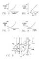
- the graph of FIG. 5indicates that the average gas bubble diameter D tends to decrease as ion implantation energy (ion kinetic energy) is decreased. Since it is important to minimize the average gas bubble diameter D, use of the torroidal source P3i reactor of FIG. 1 provides the best results, because this reactor is capable of very high implant dose rates at very low ion kinetic energy. Thus, one way of regulating the gas bubbles to a small average diameter is by using a relatively small bias power level for a small ion energy.
- the graph of FIG. 6indicates that the average gas bubble diameter D tends to decrease as the ion implantation dose (implanted atoms per square centimeter) is decreased. Therefore, another way of regulating the average gas bubble diameter D is to limit the ion implant dose of the gaseous species atoms. However, the decrease in implant dose may diminish the desired reduction in dielectric constant of the implanted insulation material, and therefore only a limited reduction in implant dosage may be preferred.
- the graph of FIG. 7indicates that the average gas bubble diameter D decreases with the temperature of the insulation layer. Therefore, it is desirable to minimize the amount of heat load on the wafer, which is readily accomplished by reducing the RF plasma source power.
- most plasma reactorshave relatively high source power threshold levels for maintaining a plasma, preventing a significant reduction in heat load.
- This problemis solved by employing the torroidal source P 3 i reactor of FIG. 1 , because this reactor can maintain a relatively dense plasma in the process region at an extremely low source power level (e.g., about 100 Watts). Accordingly, the average gas bubble diameter D is reduced by carrying out the gaseous species ion implantation in the torroidal source P 3 i reactor of FIG. 1 and using a very low source power level, as low as 100 Watts for example.
- the graph of FIG. 8indicates that the gas bubble average diameter D is less for ion implanted gas species of lesser atomic numbers. Therefore, the gas bubble average diameter D may be minimized by employing the lightest gas species for the gas bubble-forming implant step. For example, P 3 i ion implantation of the lightest gaseous species, such as hydrogen or helium, minimizes bubble diameter. However, it may be possible to achieve reasonable gas bubble sizes with heavier gaseous species, such as xenon or nitrogen, or combination of species and therefore the invention may not be limited to the lightest gaseous species.
- the foregoing parametersmay be selected to favor a smaller average gas bubble diameter D, with some of these parameters playing a larger role than others. For example, it may not be desirable to radically reduce ion dose, since that might diminish the improvement (reduction) in dielectric constant.
- the other parametersmay be optimized to the maximum, by employing a low ion energy, a low source power level (for small heat load) and using the lightest gas species (hydrogen or helium).
- FIG. 9illustrates a co-implantation process in which ion implantation of the primary species (the bubble-forming gaseous species such as hydrogen or helium) is carried out simultaneously with ion implantation of a secondary species.
- the secondary speciesmay be gaseous or non-gaseous, and enhances the properties of the ion implanted bubbles in the insulation material. Such enhancement may be promotion of a smaller average gas bubble diameter D in the insulation material or an improvement in gas bubble stability.
- An improvement in gas bubble stabilityrefers to the tendency of a bubble to migrate to and/or join another gas bubble.
- the secondary speciesmay be any one of a number of process compatible species.
- the co-implantationis achieved by introducing a precursor gas into the reactor chamber 10 containing the desired secondary species, along with the primary or gaseous species.
- the insulation materialis silicon dioxide, as indicated by the bonds between each silicon atom and pair of oxygen atoms.
- FIG. 9depicts the dielectric material as an atomic lattice of silicon atoms and oxygen atoms, each silicon atom being bound to a pair of oxygen atoms. This lattice may be referred to as the dielectric material, the dielectric layer or the insulation layer.
- Atoms of the implanted gaseous species(helium in the illustrated example of FIG. 9 ) come to rest in various locations and then migrate through the insulation layer to combine into gas bubbles 420 .
- the implanted secondary species for enhancing the gas bubble propertiesreside in distributed locations throughout the insulation material.
- the helium and phosphorus atomsmust be implanted within the same depth range, corresponding to the thickness of the insulation layer.
- the bias power (voltage) applied to the wafer support pedestalmay be shifted within a range that spans the desired implant depth range for both atomic species. This is not limited to helium and phosphorus, and combinations of species other than helium and phosphorus may be employed.
- FIGS. 10A through 10FA substrate 510 shown in FIG. 10A receives a thin (1500 angstrom) insulation layer 520 shown in FIG. 10B .
- Gas bubbles 512are formed in the thin layer 520 by ion implantation of a light gaseous species, as shown in FIG. 10C . Then, the next thin insulation layer 525 is formed over the current thin insulation layer 520 , as shown in FIG. 10D . Gas bubbles 512 are formed in the second thin insulation layer 520 by ion implantation of a light gaseous species. The process is repeated as necessary until a required number of thin layers have been deposited, each having implanted gas bubbles 512 . In this way, only a very low ion energy is required, corresponding an ion implant depth profile spanning 1500 angstroms. Such a depth profile is depicted in the graph of FIG. 10G , showing implanted gaseous species ion density in the insulation layer as a function of depth.
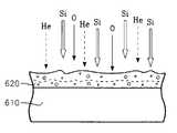
- FIGS. 11A through 11CA substrate 610 shown in FIG. 11A is exposed to a plasma formed from silane, oxygen and helium gases (other gases are possible such as SiF4, O2, He and Xe).
- the silane and oxygen gasesdissociate in the plasma into silicon, oxygen and hydrogen, the silicon and oxygen ions combining to form silicon dioxide which deposits on the top surface of the substrate of FIG. 11A to grow a silicon dioxide insulating layer 620 , as shown in FIG. 11B .
- the helium ionspenetrate the surface of the silicon dioxide layer 620 to be implanted within the silicon dioxide layer 620 .
- the heliumis implanted in a depth profile spanning a thickness of about 1500 angstroms.
- the growth rate of the silicon dioxide and the dose rate of the helium ion implantationare adjusted so that as each 1500 angstroms of the growing silicon dioxide layer receives the desired helium dose, the insulation layer has grown by about 1500 angstroms, so that the desired dose of helium atoms is implanted continuously as the insulation layer grows.
- This situationis depicted in the sequence illustrated in FIGS. 12A through 12E , showing how the silicon dioxide layer increases in thickness while the top 1500 angstroms of that layer continues to be implanted with helium atoms.
- the top surface of the insulating layercontinues to receive new silicon dioxide material and therefore is continuously rising during the helium ion implantation.
- the implanted helium atomsgather together in many small bubbles to form a matrix of gas bubbles throughout the insulation layer.
- the ion implantation processcan be employed to enhance the adhesion of an upper film of one material onto a lower film or substrate of a different material. This is because the ion implantation process carries some of the atoms of each of the two materials across the interface between the two layers.
- ion implantation of a gaseous speciesmay be used to harden a porous dielectric material, such as (for example) Black Diamond I and Black Diamond II dielectric material sold by Applied Materials, Inc, the present assignee. “Black Diamond” is a trademark of Applied Materials, Inc.
- a porous dielectric materialsuch as (for example) Black Diamond I and Black Diamond II dielectric material sold by Applied Materials, Inc, the present assignee. “Black Diamond” is a trademark of Applied Materials, Inc.
- Such porous materialshave a lower dielectric constant than silicon dioxide or other dielectrics. However, the presence of empty pores distributed throughout the material tends to reduce its mechanical hardness or strength. What is needed is a way of strengthening a porous dielectric material (increase hardness and modulus) while retaining its superior electrical characteristics (low dielectric constant).
- FIG. 13Ais a cross-sectional view of a portion of a porous dielectric material 700 having many empty pores 705 distributed throughout the volume of the material 700 .
- the porous dielectric material 700is subject to an ion implantation process in which ions 710 of a gaseous species are implanted in the material 700 .
- the implanted ions 710become neutral atoms in the dielectric material 700 and tend to migrate toward and congregate within the pores 705 . They do this to relieve stress in the lattice of the dielectric material 700 .
- the implanted gaseous species atoms 710 congregating within each pore 705form a gas 715 , as indicated in FIG. 13C .
- implanted helium atoms migrating into a porecan join together as He2 molecules within each pore 705 .
- the implanted gaseous species atoms 710are directed into the pores 705 with such a great force by the lattice strain that a significant gas pressure is created within each of the pores 705 .
- Hardening of the porous dielectric materialcan enhance its ability to withstand chemical mechanical polishing or other stressful processes. Hardening occurs as a result of densification of the low K (dielectric constant) materials. Densification tends to increase K, but because gas bubble injection reduces K, the tendency of ion implantation to increase K is cancelled.
- densificationrefers to the breaking up of pores in the porous dielectric material into smaller pores. It is believed the size of the pores in a doped low-K dielectric material (such as carbon-doped silicon dioxide) prior to densification is on the order of nanometers. The breaking up of such pores into smaller pores is the result of the impact of the implanted ions and their interaction with the bonds in the dielectric material.
- a doped low-K dielectric materialsuch as carbon-doped silicon dioxide
- Treatment of such a porous dielectric materialcan include the formation of gas bubbles as in the process depicted in FIG. 3A (to further reduce its dielectric constant), or the filling of pores with implanted gaseous species (to make it harder or stronger), as depicted in FIG. 13C .
- the same ion implantation stepcan accomplish both results, namely the formation of gas bubbles and the filling of pre-existing pores in the material.
- a co-implantation stepmay be performed as in FIG. 9 to enhance the properties of the gas bubbles. This co-implantation step is carried out in accordance with the description of FIG.
- This co-implantation stepmay be carried out before, during or after the ion implantation of the bubble-forming gaseous species.
- Ion implantationcan reduce tensile stress in the film. This is accomplished through bond breaking within the film by the implanted ions. Making the film less tensile and more compressive reduces problems such as film flaking or delamination. Therefore, ion implantation of the gaseous species to enhance the material hardness can simultaneously reduce the tensile stress of the material. Reducing the tensile stress provides better adhesion of the treated film to underlying layers, making it more resistant to delamination. In one experiment, we have found that such ion implantation can increase the hardness by as much as 50% while changing the stress from tensile (e.g., at +80 megaPascals) to compressive (e.g., at ⁇ 40 megaPascals). All this may be accomplished without increasing the dielectric constant of the treated layer. In fact, a slight improvement (decrease) in dielectric constant may be attained simultaneously with the foregoing improvements in hardness and stress.
- tensilee.g., at +80 megaPasca
- FIG. 14is a block flow diagram depicting a process sequence in accordance with an embodiment in which the dielectric layer is deposited and the bubble-forming implantation and bubble-enhancing implantation steps are performed at different times.
- the first stepis to deposit the dielectric layer (block 1410 ). This can be carried out by plasma enhanced chemical vapor deposition of silicon dioxide on a wafer in a plasma of silane and oxygen, for example.
- the next stepis to ion implant a gaseous species (e.g., hydrogen or helium) into the dielectric layer formed in the previous step.
- Another step (block 1420 )is to implant a bubble-enhancing species (e.g., boron or phosphorus) into the dielectric layer.
- a gaseous speciese.g., hydrogen or helium
- a bubble-enhancing speciese.g., boron or phosphorus
- FIG. 15is a block flow diagram depicting a process sequence in accordance with an embodiment in which gaseous bubble-forming species and the bubble-enhancing species are ion implanted in the dielectric layer simultaneously.
- the first stepis to deposit a dielectric layer (block 1510 ).
- the next stepis to introduce a process gas consisting of the gaseous bubble-forming species and a bubble-enhancing species into the plasma reactor chamber (block 1515 ).
- the next stepis to ion implant both species (block 1520 ).
- the ion implantation depth profile of each speciesmay be narrower than the thickness of the dielectric layer that is to be treated. Therefore, in the step of block 1525 , the plasma bias power is changed or swept over a continuous range so that the ion implantation depth of each of the species is swept over a range corresponding to the thickness of the dielectric layer that is to be treated.
- FIG. 16is a block flow diagram depicting a process sequence in accordance with an embodiment in which the plasma bias power is minimized, making the ion implantation depth shallow, and thin successively deposited dielectric sub-layers are deposited and ion implanted in succession.
- the successive sub-layerscan accumulate to form a thick dielectric layer.
- a very thick dielectric layermay be formed having ion implanted gas bubble-forming species using a very low ion energy (very shallow implant profile) to minimize the bubble size.
- the first stepis to deposit a thin sub-layer of dielectric material (block 1610 ).
- a gas bubble-forming speciesand optionally a bubble-enhancing species, are ion implanted into the thin dielectric sub-layer (block 1615 ).
- the next thin dielectric sub-layeris deposited over the preceding one (block 1620 ) and the ion implantation step is repeated (block 1625 ).
- the steps of 1620 and 1625are repeated in successive cycles until the desired dielectric layer thickness has been attained. The result corresponds to the illustration of FIG. 10F .
- FIG. 17illustrates another approach to minimizing ion implant energy where the final dielectric layer thickness exceeds the implant depth.
- the process of FIG. 17corresponds to the method illustrated in FIGS. 12A–12E in which the dielectric layer deposition and the bubble-forming ion implantation are performed simultaneously.
- the dielectric material precursor gasesare introduced into the plasma reactor chamber (block 1710 ). These gases may be silane and oxygen, for example, if the dielectric layer is to be silicon dioxide. Also, the gaseous (bubble-forming) species is introduced along with (optionally) a bubble-enhancing species (block 1715 ).
- a plasmais maintained in the chamber (block 1720 ), so that the dielectric material is deposited (block 1725 ) while, simultaneously, the gaseous bubble-forming species (and, optionally, the bubble-enhancing species) are implanted below the ever-rising surface of the dielectric material (block 1730 ).
- the ion energyis such that the implant ion profile is concentrated near the ever-rising surface of the dielectric layer, so that as the layer grows it is implanted throughout its entire thickness. The process continues until the desired dielectric material thickness is attained (block 1735 ).
- the overlying filmmay be a dielectric film formed on a metal film.
- the dielectric filmmay be a hard film such as SiO2, PSG or BSG, or it may be a porous film such as CSG.
- the properties of a porous dielectric film such as CSGmay be enhanced by ion implantation.
- the pores of a porous film such as CSGmay be filled with a gas by ion implantation of one of the gaseous species referred to above in this specification. This process enhances the hardness of the film. Hardening occurs as a result of densification of the low K (dielectric constant) materials. Densification tends to increase K, but because gas bubble injection reduces K, the tendency of ion implantation to increase K is cancelled or reduced. As a result, hardening of the material can be carried out without increasing the dielectric constant of the material.
- porous dielectric filmAnother property of a porous dielectric film that may be enhanced by ion implantation is stress. Specifically, porous films tend to have relatively high tensile stress, and as a result are susceptible to flaking and delamination. Ion implantation tends to break a small proportion of the atomic bonds within the porous layer, which changes the stress within the layer from tensile to compressive. The transition reduces the porous film's susceptibility to flaking or delamination.
- the ion implantation process for improving the mechanical properties of a porous dielectric layerhas been described with reference to ion implantation of a gaseous species such as hydrogen, nitrogen or one of the inert gas species.
- a gaseous speciessuch as hydrogen, nitrogen or one of the inert gas species.
- a non-gaseous speciesmay be employed in such a process.
- the non-gaseous speciesis preferably a process-compatible semiconductor species, such as (for example) germanium, silicon, carbon, or non-conductor species such as (for example) boron, arsenic, phosphorus, and the like.
- the entire processconsists of, first, obtaining a dielectric layer that has been doped so as to reduce its dielectric constant.
- Thismay be accomplished, for example, by forming a silicon dioxide layer doped with carbon, using chemical vapor deposition or other suitable techniques.
- a silicon dioxide layer doped with carbontends to be porous and tends to have significant tensile stress. Then, the hardness of the material is improved and the tensile stress of the material is reduced by ion implanting one of the non-gaseous species listed immediately above.
- a porous low-dielectric constant materialsuch as carbon-doped silicon dioxide
- enhancing the hardness of that materialcan be accomplished simultaneously in a single ion implantation step.
- a pure (or nearly pure) dielectric layersuch as silicon dioxide
- the dielectric layere.g., SiO2
- a first speciese.g., carbon
- a second speciese.g., hydrogen
- Such a simultaneous ion implantation processmay be carried out by plasma immersion ion implantation using a process gas whose constituents are the first and second species.
- Ion implantation of the first speciese.g., carbon
- ion implantation of the second speciese.g., hydrogen
- Such a process gasmay contain carbon and hydrogen as the first and second species, respectively (in which case the process gas could be methane or acetylene).
- the first speciesmay be another species such as boron, for example, so that the process gas could consist of boron and hydrogen (B2H6), for example.
- the dielectric material that is treated in this mannermay be silicon dioxide or silicon nitride, for example.
- the second species that enhances the mechanical properties of the dielectric layermay be a non-gaseous species of the type listed above (germanium, silicon, carbon, boron, arsenic, phosphorus, and the like).
- This ion implantation processmay be followed immediately by a post-implant annealing step in which the wafer temperature is raised to an elevated temperature less than about 400 degrees C. It is believed that such an elevated temperature promotes the formation of the optimum molecular species for reducing the dielectric constant K of the implanted dielectric material.
- Each of the ion implantation steps described abovemay be followed by post-implant annealing at temperatures less than 400 degrees C. to stabilize the effects of ion implantation. Such temperatures do not distort the process because in standard integration thermal processes, such temperatures are used for various processes such as CVD film deposition.
- Post-implant annealingis not needed if the ion implantation is performed at a high wafer temperature (e.g., above 500 degrees C.).
- a high wafer temperaturee.g., above 500 degrees C.
- a slight penaltyis incurred because the tensile stress increases (slightly). In one example, this increase was from ⁇ 40 megaPascal to ⁇ 10 megaPascal, which nevertheless left a great improvement from the pre-implant stress level of the material (+80 megaPascal).
Landscapes
- Engineering & Computer Science (AREA)
- Physics & Mathematics (AREA)
- Plasma & Fusion (AREA)
- Chemical & Material Sciences (AREA)
- Analytical Chemistry (AREA)
- Condensed Matter Physics & Semiconductors (AREA)
- General Physics & Mathematics (AREA)
- Manufacturing & Machinery (AREA)
- Computer Hardware Design (AREA)
- Microelectronics & Electronic Packaging (AREA)
- Power Engineering (AREA)
- Internal Circuitry In Semiconductor Integrated Circuit Devices (AREA)
Abstract
Description
This application is a continuation-in-part of U.S. application Ser. No. 10/838,052 filed May 3, 2004 entitled LOW TEMPERATURE CVD PROCESS WITH CONFORMALITY, STRESS AND COMPOSITION by Hiroji Hanawa, et al., the disclosure of which is incorporated herein by reference and of which is a continuation-in-part of U.S. patent application Ser. No. 10/786,410 filed Feb. 24, 2004 now U.S. Pat. 6,893,907 entitled FABRICATION OF SILICON-ON-INSULATOR STRUCTURE USING PLASMA IMMERSION ION IMPLANTATION by Dan Maydan et al., which is a continuation-in-part of U.S. patent application Ser. No. 10/646,533 filed Aug. 22, 2003 entitled PLASMA IMMERSION ION IMPLANTATION PROCESS USING A PLASMA SOURCE HAVING LOW DISSOCIATION AND LOW MINIMUM PLASMA VOLTAGE by Kenneth Collins et al., which is a continuation-in-part of U.S. patent application Ser. No. 10/164,327 filed Jun. 5, 2003 now U.S. Pat. No. 6,939,434 entitled EXTERNALLY EXCITED TORROIDAL PLASMA SOURCE WITH MAGNETIC CONTROL OF ION DISTRIBUTION by Kenneth Collins et al., which is a continuation-inpart of U.S. patent application Ser. No. 09/636,435 filed Aug. 11, 2000 entitled EXTERNALLY EXCITED MULTIPLE TORROIDAL PLASMA SOURCE by Hiroji Hanawa et al., now issued as U.S. Pat. No. 6,494,986 B1, all of which are assigned to the present assignee.
With recent advances in integrated circuit design, there are now as many as six to ten insulated interconnect layers overlying the semiconductor transistors for devices using the current 90 nm design rules. The next generation may employ 35 nm design rules and may have as many as 12 to 14 insulated interconnect layers. These interconnect layers can have completely different conductor patterns and are connected to one another and to the transistor layer at different locations through contact vias extending vertically between the horizontal layers. It is the formation of the contact vias with which the present invention is concerned.
Due to the large number of interconnect layers and the total electrical path length they represent, the interconnect layers account for a significant proportion if not a majority of the total power losses in the integrated circuit.
To reduce resistive power losses in the integrated circuit, the interconnect layers and the contact vias typically employ copper as the principal conductor and silicon dioxide as the insulator. Because copper tends to diffuse through the silicon dioxide insulator material, a barrier layer is placed between the copper material and the silicon dioxide material wherever the two materials interface in the integrated circuit. The barrier layer is typically formed of an underlying tantalum nitride layer contacting the silicon dioxide insulator, and overlying pure (or nearly pure) tantalum layer and, finally, a copper seed layer over the pure tantalum layer. The copper conductor is deposited on the copper seed layer. Such a barrier layer prevents migration or diffusion of copper atoms into the silicon dioxide insulator material.
In order to reduce power losses and interference by capacitive coupling between adjacent interconnect layers, it is desirable to employ an insulating material with the lowest possible dielectric constant. Silicon dioxide can be employed because it has superior mechanical properties. However, silicon dioxide has a relatively high dielectric constant (about 4.0) and is therefore not ideal. It has been found that combining silicon dioxide with a species such as boron or phosphorus produces a glassy material having a lower dielectric constant. For example, combining silicon dioxide with boron produces boron silicate glass (BSG). BSG has a dielectric constant of 3.2. Other insulator materials have been developed having even lower dielectric constants, such as insulation material sold by Applied Materials, Inc., the present assignee, under the trademarks Black Diamond I (dielectric constant of <3.0) and Black Diamond II (dielectric constant of <2.6). These materials with such low dielectric constants provide very good electrical performance with minimum capacitive coupling between interconnect layers. Unfortunately, their mechanical properties are inferior to those of silicon dioxide because these materials tend to be porous and therefore are not as hard as silicon dioxide. This is a particularly difficult problem because the insulator layer deposited over an interconnect layer tends to form a very uneven top surface and must therefore be smoothed to a plane surface by chemical mechanical polishing. While silicon dioxide is a sufficiently hard material to be relatively impervious to flaking or cracking during chemical mechanical polishing, porous materials with low dielectric constant can be susceptible to damage during chemical mechanical polishing.
Therefore, what is needed is a hard insulator material having a low dielectric constant that can reliably withstand chemical mechanical polishing. Currently available insulator materials suitable for use in multiple interconnect layers of integrated circuits are either porous and weak or else have a relatively high dielectric constant.
An integrated microelectronic circuit has a multi-layer interconnect structure overlying the transistors consisting of stacked metal pattern layers and insulating layers separating adjacent ones of said metal pattern layers. Each of the insulating layers is a dielectric material with plural gas bubbles distributed within the volume of the dielectric material to reduce its dielectric constant, the gas bubbles being formed by ion implantation of a gaseous species into the dielectric material.
The method can include regulating the average diameter of the gas bubbles by regulating the energy of the ions of the gaseous species during the step of ion implanting, or by regulating the temperature of the workpiece during the ion implanting step or by regulating the ion implantation dose of the ion implantation step, or by ion implanting a bubble-enhancing species. The gaseous species can be a light, heavy or combination of light and heavy gaseous species (e.g, H, He, Ar, Xe, H and He, He and Xe, F and Xe, H and Ar, etc).
The step of ion implanting can be carried out by plasma immersion ion implantation in a torroidal source plasma reactor having at least one external reentrant conduit, by introducing a process gas comprising a precursor of the gaseous species to be ion implanted, and then coupling RF power to process gases in the reentrant conduit to generate an oscillating plasma current in a torroidal path that includes the reentrant conduit and a process zone adjacent the surface of the workpiece. The ion energy and implant depth profile is controlled by applying RF plasma bias power to the workpiece.
In the present invention, an insulating material having excellent mechanical properties but poor electrical properties (a relatively high dielectric constant) is subject to ion implantation of a light gaseous species such as hydrogen or helium. The ion energy and dosage of the implantation process and the temperature of the insulating material are selected so that implanted atoms of the gaseous species inside the insulating material migrate or coalesce toward one another to form small gas bubbles throughout the insulating material. The gas bubbles within the insulating material have a very low dielectric constant (e.g., about 1.04). The result is that the total dielectric constant of the insulating layer is significantly reduced due to the presence of the bubbles. In the case of silicon dioxide containing bubbles formed by ion implantation of a gaseous species, the dielectric constant may be as low as 3.5. The reduction in dielectric constant depends upon the proportion of the volume within the insulating material occupied by the gas bubbles.
Other “bubble-enhancing” species, both gaseous and non-gaseous, may be implanted in addition to the gaseous species. The “enhancing” species may promote small bubble size. Also or alternatively, the “enhancing” species may promote bubble stability within the insulator (to avoid bubble growth or conjoining of adjacent bubbles). Small bubble size is desirable in order to ensure a smooth insulator material surface after etching or chemical mechanical polishing. Good bubble stability is desirable to permit close spacing between bubbles and a concomitantly higher bubble density within the insulating material for greater reduction in dielectric constant.
In accordance with another aspect of the invention, materials having superior electrical properties but inferior mechanical properties relative to silicon dioxide can have their mechanical properties improved without compromising their superior electrical properties. Examples of such materials include carbon-doped silicon dioxide, formed in a plasma containing silicon dioxide precursors (silane and oxygen) and a carbon precursor. Such materials tend to be porous and therefore mechanically weaker. Their superior electrical property is a dielectric constant (electrical permittivity) that is lower than that of silicon dioxide. Such materials may have their mechanical properties improved by ion implantation of a light gaseous species. In this process, ion implant dosage and energy and material temperature are selected so that the implanted gaseous species atoms gather within the empty pores of the insulator material to form a pressurized gas inside each pore. With each pore thus internally pressurized, the compressive strength or hardness of the insulator material is enhanced. Such a process may in some cases be referred to as a “hardening ion implantation” step. Ion implantation can also reduce tensile stress in the film (making it more compressive) through bond breaking and formation of damage.
In accordance with a yet further aspect of the invention, the porous material that has been mechanically improved by the foregoing “hardening ion implantation” step may also be electrically improved by the bubble-forming ion implantation step previously described. In this ion implantation step, a light gaseous species is implanted in the insulator material with the implant energy and dosage and material temperature adjusted so that the implanted gaseous atoms migrate toward one another within local regions to form gas bubbles within the material. These gas bubbles may be about 1–5 nm in diameter, which may be about the same size or smaller than the pores of the porous material. This addition of gas bubbles into the porous insulator material reduces its dielectric constant from its nominal value (e.g., <3.0 or <2.6 for carbon-doped silicon dioxide) to a lower level.
In a related aspect, the “hardening ion implantation” step and the bubble-formation ion implantation step may be one and the same ion implantation step or may be performed as part of the same ion implantation process, with the process parameters being changed during implantation to perform bubble formation, and then (or beforehand) hardening.
An important aspect is the ability to control both ion implantation dosage and ion energy in order to control bubble size. A lower ion energy enables the process to form smaller and more numerous bubbles. On the other hand, an entire wafer must be implanted, and therefore a large ion flux is necessary to complete the implantation process within a reasonable amount of time. In view of these requirements, the preferred way of performing the bubble-forming ion implantation step is to employ a torroidal source plasma ion immersion implantation reactor described in the above-referenced parent application. This is because such a reactor is capable of very high maximum ion flux and a very low minimum ion energy. In addition, in order to minimize the material temperature during ion implantation (to minimize bubble size), the minimum plasma source power level in such a reactor is extremely low, relative to other plasma immersion ion implantation reactors. By minimizing plasma source power, the temperature of the insulator material during ion implantation can be significantly reduced to achieve a minimum bubble size. Such a reactor, adapted particularly for bubble-forming ion implantation, is illustrated inFIG. 1 .
Referring now toFIG. 1 , a torroidal source plasma immersion ion implantation (“P3I”) reactor of the type disclosed in the above-reference parent application has acylindrical vacuum chamber 10 defined by acylindrical side wall 12 and a disk-shapedceiling 14. Awafer support pedestal 16 at the floor of the chamber supports asemi-conductor wafer 18 to be processed. A gas distribution plate orshowerhead 20 on theceiling 14 receives process gas in itsgas manifold 22 from agas distribution panel 24 whose gas output can be any one of or mixtures of gases from individual gas supplies26a–26jof hydrogen, helium, phosphorus-containing gas, boron-containing gas, a carbon-containing gas, nitrogen, silane, germanium-hydride gas, krypton, xenon, argon, respectively. Avacuum pump 28 is coupled to a pumpingannulus 30 defined between thewafer support pedestal 16 and thesidewall 12. Aprocess region 32 is defined between thewafer 18 and thegas distribution plate 20.
A pair of externalreentrant conduits process region 32. Each of theconduits ends 38 coupled to opposite sides of the chamber. Eachconduit conduit D.C. insulation ring 40 preventing the formation of a closed loop conductive path between the two ends of the conduit.
An annular portion of eachconduit magnetic core 42. Anexcitation coil 44 surrounding thecore 42 is coupled to anRF power source 46 through animpedance match device 48. The twoRF power sources 46 coupled to respective ones of thecores 44 may be of two slightly different frequencies. The RF power coupled from theRF power generators 46 produces plasma ion currents in closed torroidal paths extending through therespective conduit process region 32. These ion currents oscillate at the frequency of the respectiveRF power source wafer support pedestal 16 by abias power generator 49 through animpedance match circuit 50.
Plasma immersion ion implantation of thewafer 18 is performed by introducing a gas or multiple of gases containing the species to be ion implanted into thechamber 32 through thegas distribution plate 20 and applying sufficient source power from thegenerators 46 to thereentrant conduits process region 32. The ion implantation depth is determined by the wafer bias voltage applied by the RFbias power generator 49. The ion implantation rate or flux (number of ions implanted per square cm per second) is determined by the plasma density, which is controlled by the level of RF power applied by the RFsource power generators 46. The cumulative implant dose (ions/square cm) in thewafer 18 is determined by both the flux and the total time over which the flux is maintained.
If thewafer support pedestal 16 is an electrostatic chuck, then a buriedelectrode 52 is provided within an insulatingplate 54 of the wafer support pedestal, and the buriedelectrode 52 is coupled to thebias power generator 49 through theimpedance match circuit 50. Thewafer support pedestal 16 may be of the type disclosed inFIGS. 97 and 98 of the above-referenced parent application.
The dielectric constant (electrical permittivity) of an insulating layer on a semiconductor wafer is reduced by placing thewafer 18 on thewafer support pedestal 16, introducing a gaseous species into thechamber 10 and striking a plasma so that the gaseous species is ion implanted into the insulating layer. The wafer bias voltage delivered by the RFbias power generator 49 is adjusted so that the implant depth of the gaseous species is within the insulating layer. The gaseous species may be any one of or combination of hydrogen, helium, nitrogen, neon, argon, krypton, xenon, fluorine, chlorine, iodine, bromine, oxygen.
ThePMOS transistor 102 includes heavily p-doped source and drainregions extensions channel 112. A polycrystalline silicon gate electrode114 overlies thechannel 112 and is separated from it by a thin gatesilicon dioxide layer 116. A titanium silicide (or cobalt silicide) gate contact118 overlies the gate electrode114. A titanium silicide (or cobalt silicide)source contact region 120 is formed in thesource region 108a. A siliconnitride insulation layer 122 overlies the source and drainregion gate electrode structure 114,116,118.Silicon dioxide islands 124 lie within theinsulation layer 122. A thin silicon nitrideetch stop layer 126 overlies thePMOS transistor 102. Thebottom insulation layer 130 of what will become an overlyingmultiple interconnect layer 132 overlies theetch stop layer 126. After theinsulation layer 130 is formed, it is subjected to a chemical mechanical polishing process to render itstop surface 130aperfectly flat as illustrated inFIG. 2A . A metallic (e.g., tin)source contact 134 extends vertically through theinsulation layer 130 and through theetch stop layer 126 to the titanium silicidesource contact region 120. The insulation layer may be silicon dioxide (SiO2), or silicon dioxide-containing combinations such as phosphorus silicate glass (PSG), boron silicate glass (BSG) or carbon-doped silicate glass (CSG). Such combinations can be formed in a plasma-enhanced deposition process using a process gas containing a silicon precursor (e.g., silane), oxygen and a phosphorus precursor gas (PH3) or a boron precursor gas (B2H6) or a carbon-containing gas.
TheNMOS transistor 202 includes heavily n-doped source and drainregions extensions channel 212. A polycrystallinesilicon gate electrode 214 overlies thechannel 212 and is separated from it by a thin gatesilicon dioxide layer 216. A titaniumsilicide gate contact 218 overlies thegate electrode 214. A titanium silicidesource contact region 220 is formed in thesource region 208a. A siliconnitride insulation layer 222 overlies the source and drainregion gate electrode structure Silicon dioxide islands 224 lie within theinsulation layer 222. A thin silicon nitrideetch stop layer 226 overlies theNMOS transistor 202. Thebottom insulation layer 130 of the overlyingmultiple interconnect layer 132 overlies theetch stop layer 226. A metallic (e.g., TiN)drain contact 234 extends vertically through theinsulation layer 130 and through theetch stop layer 226 to the titanium silicidesource contact region 220.
The insulating layer130 (which may be, for example, PSG, BSG, CSG or SiO2) is unique in that it holds a three-dimensional matrix of gas bubbles formed by ion implantation of a gaseous species.FIG. 2A depicts the performance of this ion implantation step, as carried out (preferably) in the torroidal source P3i reactor ofFIG. 1 . In this step, thefirst insulation layer 130 of themultiple interconnect layer 132 has been deposited, and is completely exposed. The plasma consists ofions 140 of a light gaseous species, such as hydrogen or helium, for example. Theions 140 are accelerated down to thewafer 18 to be implanted in theinsulator layer 130 by the wafer bias voltage from the RFbias power generator 49 ofFIG. 1 applied to thesupport pedestal electrode 52. The implanted gaseous species atoms within the insulator layer migrate toward one another to gather in many small gas bubbles142 distributed throughout theinsulator layer 130. Ideally, the gas bubbles142 are very small (about 1–5 nm in diameter) and are distributed uniformly throughout theinsulator layer 130 as a three-dimensional matrix of gas bubbles. Depending upon the temperature of the post-implantation anneal process, the implanted gas species may evolve out of the material or coalesce to form larger gas bubbles. Such bubbles are very stable and may not burst till reaching the melting temperature of the materials. These bubbles represent regions of lower dielectric constant relative to the solid portions of the film.
The spacing or density of the gas bubbles330 within the insulatinglayer 320 determines the reduction of the dielectric constant of the insulatinglayer 320. This is because the reduction in the dielectric constant of the insulatinglayer 320 is determined at least in large part by the proportion of volume within the insulatinglayer 320 occupied by all the gas bubbles. This is depicted in the graph ofFIG. 3B , showing how the dielectric constant, k, is 4 in the case of pure silicon dioxide, and is slight over 1 in the case of pure helium gas. As the total volume occupied by the gas bubbles within the insulatinglayer 320 increases from zero towards 50%, the dielectric constant, k, decreases from 4 to about 2.5. Therefore the smaller the spacing S betweenbubbles 330, the greater the volume occupied by gas in the insulator layer, and therefore the more the dielectric constant is decreased.
With regard to chemical mechanical polishing, theinsulator layer 410 initially has a rough ornon-planar surface 410aimmediately following its formation, as indicated in dashed line. In order to form a high quality conductor pattern over the insulator, it must first be chemically mechanically polished. This removes atop layer 410bof the material410 to form a smooth planar surface410c. However, prior to the chemical mechanical polishing step that removed thetop layer 410b, some of the gas bubbles420 lay across the boundary that eventually became the planar surface410c, and may be referred to as boundary gas bubbles420′. The boundary gas bubbles420′ are cut open and become small holes upon removal of thetop layer 410b. As a result, the otherwise smooth surface410chas holes in it. These holes have no effect upon subsequent process steps (e.g., deposition of a metal conductor pattern on the top surface410c) provided the hole size (bubble diameter D) is small. For this purpose, the bubble diameter is preferably within a range of 1–5 nm.
There are several ways for regulating the average bubble size. These include selecting ion energy (by selecting plasma bias power), controlling ion implant dose (by controlling plasma ion density and process time), controlling the wafer temperature and selecting a gas species of a particular atomic number, and co-implanting non-gaseous or gaseous species that promotes bubble stability and/or small bubble size. Each of these approaches will now be discussed.
The graph ofFIG. 5 indicates that the average gas bubble diameter D tends to decrease as ion implantation energy (ion kinetic energy) is decreased. Since it is important to minimize the average gas bubble diameter D, use of the torroidal source P3i reactor ofFIG. 1 provides the best results, because this reactor is capable of very high implant dose rates at very low ion kinetic energy. Thus, one way of regulating the gas bubbles to a small average diameter is by using a relatively small bias power level for a small ion energy.
The graph ofFIG. 6 indicates that the average gas bubble diameter D tends to decrease as the ion implantation dose (implanted atoms per square centimeter) is decreased. Therefore, another way of regulating the average gas bubble diameter D is to limit the ion implant dose of the gaseous species atoms. However, the decrease in implant dose may diminish the desired reduction in dielectric constant of the implanted insulation material, and therefore only a limited reduction in implant dosage may be preferred.
The graph ofFIG. 7 indicates that the average gas bubble diameter D decreases with the temperature of the insulation layer. Therefore, it is desirable to minimize the amount of heat load on the wafer, which is readily accomplished by reducing the RF plasma source power. However, most plasma reactors have relatively high source power threshold levels for maintaining a plasma, preventing a significant reduction in heat load. This problem is solved by employing the torroidal source P3i reactor ofFIG. 1 , because this reactor can maintain a relatively dense plasma in the process region at an extremely low source power level (e.g., about 100 Watts). Accordingly, the average gas bubble diameter D is reduced by carrying out the gaseous species ion implantation in the torroidal source P3i reactor ofFIG. 1 and using a very low source power level, as low as 100 Watts for example.
The graph ofFIG. 8 indicates that the gas bubble average diameter D is less for ion implanted gas species of lesser atomic numbers. Therefore, the gas bubble average diameter D may be minimized by employing the lightest gas species for the gas bubble-forming implant step. For example, P3i ion implantation of the lightest gaseous species, such as hydrogen or helium, minimizes bubble diameter. However, it may be possible to achieve reasonable gas bubble sizes with heavier gaseous species, such as xenon or nitrogen, or combination of species and therefore the invention may not be limited to the lightest gaseous species.
The foregoing parameters (ion energy, ion dose, wafer temperature and atomic weight) may be selected to favor a smaller average gas bubble diameter D, with some of these parameters playing a larger role than others. For example, it may not be desirable to radically reduce ion dose, since that might diminish the improvement (reduction) in dielectric constant. The other parameters may be optimized to the maximum, by employing a low ion energy, a low source power level (for small heat load) and using the lightest gas species (hydrogen or helium).
InFIG. 9 , the insulation material is silicon dioxide, as indicated by the bonds between each silicon atom and pair of oxygen atoms.FIG. 9 depicts the dielectric material as an atomic lattice of silicon atoms and oxygen atoms, each silicon atom being bound to a pair of oxygen atoms. This lattice may be referred to as the dielectric material, the dielectric layer or the insulation layer. Atoms of the implanted gaseous species (helium in the illustrated example ofFIG. 9 ) come to rest in various locations and then migrate through the insulation layer to combine into gas bubbles420. The implanted secondary species for enhancing the gas bubble properties (phosphorus in the illustrated example ofFIG. 9 ) reside in distributed locations throughout the insulation material. The helium and phosphorus atoms must be implanted within the same depth range, corresponding to the thickness of the insulation layer. In order to ensure that the heavier secondary atoms and the light primary atoms are implanted in the same depth range (corresponding to the thickness of the insulation layer), the bias power (voltage) applied to the wafer support pedestal may be shifted within a range that spans the desired implant depth range for both atomic species. This is not limited to helium and phosphorus, and combinations of species other than helium and phosphorus may be employed.
In order to help minimize the gas bubble average diameter D, the ion energy should be reduced or minimized. But this limits the ion implantation depth profile. In attempting to form gas bubbles in a very thick insulation layer, the layer thickness may exceed the implant depth range for a very low energy ion implantation process. One way around this problem is to form the thick insulation layer by successive depositions of very thin insulation layers, and conduct a bubble-forming gas species ion implantation step after the formation of each of the successive thin insulation layers. Such a procedure is depicted inFIGS. 10A through 10F . Asubstrate 510 shown inFIG. 10A receives a thin (1500 angstrom)insulation layer 520 shown inFIG. 10B . Gas bubbles512 are formed in thethin layer 520 by ion implantation of a light gaseous species, as shown inFIG. 10C . Then, the nextthin insulation layer 525 is formed over the currentthin insulation layer 520, as shown inFIG. 10D . Gas bubbles512 are formed in the secondthin insulation layer 520 by ion implantation of a light gaseous species. The process is repeated as necessary until a required number of thin layers have been deposited, each having implanted gas bubbles512. In this way, only a very low ion energy is required, corresponding an ion implant depth profile spanning 1500 angstroms. Such a depth profile is depicted in the graph ofFIG. 10G , showing implanted gaseous species ion density in the insulation layer as a function of depth.
Another procedure for minimizing the required ion energy to form gas bubbles by ion implantation of a very thick insulation layer is to form the thick insulation layer by deposition of the insulator material (e.g., silicon dioxide) at a controlled rate. Simultaneously with the deposition, gaseous species are implanted at a shallow depth below the surface of the continuously thickening insulation layer, so that the surface is continually rising. In this way, the implantation depth profile can be extremely shallow regardless of the ultimate thickness of the deposited insulation layer. Such a procedure is illustrated inFIGS. 11A through 11C . Asubstrate 610 shown inFIG. 11A is exposed to a plasma formed from silane, oxygen and helium gases (other gases are possible such as SiF4, O2, He and Xe). The silane and oxygen gases dissociate in the plasma into silicon, oxygen and hydrogen, the silicon and oxygen ions combining to form silicon dioxide which deposits on the top surface of the substrate ofFIG. 11A to grow a silicondioxide insulating layer 620, as shown inFIG. 11B . Simultaneously, the helium ions penetrate the surface of thesilicon dioxide layer 620 to be implanted within thesilicon dioxide layer 620. The helium is implanted in a depth profile spanning a thickness of about 1500 angstroms. The growth rate of the silicon dioxide and the dose rate of the helium ion implantation are adjusted so that as each 1500 angstroms of the growing silicon dioxide layer receives the desired helium dose, the insulation layer has grown by about 1500 angstroms, so that the desired dose of helium atoms is implanted continuously as the insulation layer grows. This situation is depicted in the sequence illustrated inFIGS. 12A through 12E , showing how the silicon dioxide layer increases in thickness while the top 1500 angstroms of that layer continues to be implanted with helium atoms. The top surface of the insulating layer continues to receive new silicon dioxide material and therefore is continuously rising during the helium ion implantation. The implanted helium atoms gather together in many small bubbles to form a matrix of gas bubbles throughout the insulation layer.
The ion implantation process can be employed to enhance the adhesion of an upper film of one material onto a lower film or substrate of a different material. This is because the ion implantation process carries some of the atoms of each of the two materials across the interface between the two layers.
In accordance with another aspect, ion implantation of a gaseous species may be used to harden a porous dielectric material, such as (for example) Black Diamond I and Black Diamond II dielectric material sold by Applied Materials, Inc, the present assignee. “Black Diamond” is a trademark of Applied Materials, Inc. Such porous materials have a lower dielectric constant than silicon dioxide or other dielectrics. However, the presence of empty pores distributed throughout the material tends to reduce its mechanical hardness or strength. What is needed is a way of strengthening a porous dielectric material (increase hardness and modulus) while retaining its superior electrical characteristics (low dielectric constant).
Treatment of such a porous dielectric material can include the formation of gas bubbles as in the process depicted inFIG. 3A (to further reduce its dielectric constant), or the filling of pores with implanted gaseous species (to make it harder or stronger), as depicted inFIG. 13C . Alternatively, the same ion implantation step can accomplish both results, namely the formation of gas bubbles and the filling of pre-existing pores in the material. In conjunction with gas bubble-forming ion implantation in a porous material, a co-implantation step may performed as inFIG. 9 to enhance the properties of the gas bubbles. This co-implantation step is carried out in accordance with the description ofFIG. 9 , in which a material such as phosphorus, boron or Xe is ion implanted in the dielectric material. This co-implantation step may be carried out before, during or after the ion implantation of the bubble-forming gaseous species.
Ion implantation can reduce tensile stress in the film. This is accomplished through bond breaking within the film by the implanted ions. Making the film less tensile and more compressive reduces problems such as film flaking or delamination. Therefore, ion implantation of the gaseous species to enhance the material hardness can simultaneously reduce the tensile stress of the material. Reducing the tensile stress provides better adhesion of the treated film to underlying layers, making it more resistant to delamination. In one experiment, we have found that such ion implantation can increase the hardness by as much as 50% while changing the stress from tensile (e.g., at +80 megaPascals) to compressive (e.g., at −40 megaPascals). All this may be accomplished without increasing the dielectric constant of the treated layer. In fact, a slight improvement (decrease) in dielectric constant may be attained simultaneously with the foregoing improvements in hardness and stress.
Enhancement of Film Properties by Ion Implantation:
Adhesion between films is enhanced by ion implantation. Kinetic energy of the incident ions moves a portion of the atoms in each of the adjacent layers across the boundary between the two layers. This increases the thickness of the boundary region (straddling the interface between the two layer) occupied by atoms of the two different layers, thereby increasing the number of bonds between atoms of the two different layers. The result is a stronger bond between the two layers. Such adhesion-enhancement can be obtained using any of the ion implantation processes described above in this specification. Such results are described in the above-referenced parent application with reference toFIGS. 118A through 118C and119A through119C. The overlying film may be a dielectric film formed on a metal film. The dielectric film may be a hard film such as SiO2, PSG or BSG, or it may be a porous film such as CSG.
The properties of a porous dielectric film such as CSG may be enhanced by ion implantation. As described above with reference toFIGS. 13A through 13C , the pores of a porous film such as CSG may be filled with a gas by ion implantation of one of the gaseous species referred to above in this specification. This process enhances the hardness of the film. Hardening occurs as a result of densification of the low K (dielectric constant) materials. Densification tends to increase K, but because gas bubble injection reduces K, the tendency of ion implantation to increase K is cancelled or reduced. As a result, hardening of the material can be carried out without increasing the dielectric constant of the material.
Another property of a porous dielectric film that may be enhanced by ion implantation is stress. Specifically, porous films tend to have relatively high tensile stress, and as a result are susceptible to flaking and delamination. Ion implantation tends to break a small proportion of the atomic bonds within the porous layer, which changes the stress within the layer from tensile to compressive. The transition reduces the porous film's susceptibility to flaking or delamination.
The ion implantation process for improving the mechanical properties of a porous dielectric layer, (e.g., by increasing its hardness or reducing its tensile stress), has been described with reference to ion implantation of a gaseous species such as hydrogen, nitrogen or one of the inert gas species. However, a non-gaseous species may be employed in such a process. The non-gaseous species is preferably a process-compatible semiconductor species, such as (for example) germanium, silicon, carbon, or non-conductor species such as (for example) boron, arsenic, phosphorus, and the like. The entire process consists of, first, obtaining a dielectric layer that has been doped so as to reduce its dielectric constant. This may be accomplished, for example, by forming a silicon dioxide layer doped with carbon, using chemical vapor deposition or other suitable techniques. Such a low-K material tends to be porous and tends to have significant tensile stress. Then, the hardness of the material is improved and the tensile stress of the material is reduced by ion implanting one of the non-gaseous species listed immediately above.
Formation of a porous low-dielectric constant material (such as carbon-doped silicon dioxide) and enhancing the hardness of that material can be accomplished simultaneously in a single ion implantation step. First, a pure (or nearly pure) dielectric layer (such as silicon dioxide) is deposited using a process such as plasma enhanced chemical vapor deposition. Then, using plasma immersion ion implantation of the type described above, the dielectric layer (e.g., SiO2) is implanted with a first species (e.g., carbon) that reduces its dielectric constant and simultaneously implanted with a second species (e.g., hydrogen) that improves its mechanical properties (increasing hardness and reducing tensile stress). Such a simultaneous ion implantation process may be carried out by plasma immersion ion implantation using a process gas whose constituents are the first and second species. Ion implantation of the first species (e.g., carbon) reduces the dielectric constant through changes in the chemical properties of the dielectric material, while ion implantation of the second species (e.g., hydrogen) changes the material through mechanical changes in the dielectric material (e.g., the filling of voids with the second species). Such a process gas may contain carbon and hydrogen as the first and second species, respectively (in which case the process gas could be methane or acetylene). The first species may be another species such as boron, for example, so that the process gas could consist of boron and hydrogen (B2H6), for example. The dielectric material that is treated in this manner may be silicon dioxide or silicon nitride, for example. Moreover, as discussed in the preceding paragraph, the second species that enhances the mechanical properties of the dielectric layer may be a non-gaseous species of the type listed above (germanium, silicon, carbon, boron, arsenic, phosphorus, and the like). This ion implantation process may be followed immediately by a post-implant annealing step in which the wafer temperature is raised to an elevated temperature less than about 400 degrees C. It is believed that such an elevated temperature promotes the formation of the optimum molecular species for reducing the dielectric constant K of the implanted dielectric material.
Each of the ion implantation steps described above may be followed by post-implant annealing at temperatures less than 400 degrees C. to stabilize the effects of ion implantation. Such temperatures do not distort the process because in standard integration thermal processes, such temperatures are used for various processes such as CVD film deposition. Post-implant annealing, however, is not needed if the ion implantation is performed at a high wafer temperature (e.g., above 500 degrees C.). When such post-implant annealing is performed immediately following an implantation process for reducing tensile stress (described above in this specification), a slight penalty is incurred because the tensile stress increases (slightly). In one example, this increase was from −40 megaPascal to −10 megaPascal, which nevertheless left a great improvement from the pre-implant stress level of the material (+80 megaPascal).
While the invention has been described in detail by specific reference to preferred embodiments, it is understood that variations and modifications thereof may be made without departing from the true spirit and scope of the invention.
Claims (38)
1. A method of forming a low dielectric constant insulating film on a workpiece, comprising:
forming a dielectric layer on said workpiece; and ion implanting a gaseous species into said dielectric layer so as to form gas bubbles in said dielectric layer;
regulating the average diameter of said gas bubbles by regulating the energy of the ions of said gaseous species during the step of ion implanting.
2. A method of forming a low dielectric constant insulating film on a workpiece, comprising:
forming a dielectric layer on said workpiece; and
ion implanting a gaseous species into said dielectric layer so as to form gas bubbles in said dielectric layer;
regulating the average diameter of said gas bubbles by regulating the temperature of said workpiece during the ion implanting step.
3. A method of forming a low dielectric constant insulating film on a workpiece, comprising:
forming a dielectric layer on said workpiece; and
ion implanting a gaseous species into said dielectric layer so as to form gas bubbles in said dielectric layer;
regulating the average diameter of said bubbles by regulating the ion implantation dose of the ion implantation step.
4. A method of forming a low dielectric constant insulating film on a workpiece, comprising:
forming a dielectric layer on said workpiece; and
ion implanting a gaseous species into said dielectric layer so as to form gas bubbles in said dielectric layer;
regulating the average diameter of said bubbles by ion implanting a bubble-enhancing species.
5. The method ofclaim 4 wherein said bubble-enhancing species comprises one of boron, phosphorus, arsenic, carbon, germanium.
6. The method ofclaim 5 wherein said gaseous species comprises one or combination of hydrogen, helium, nitrogen, argon, xenon, neon, krypton, fluorine, chlorine, iodine, bromine, oxygen.
7. A method of forming a low dielectric constant insulating film on a workpiece, comprising:
forming a dielectric layer on said workpiece; and
ion implanting a gaseous species into said dielectric layer so as to form gas bubbles in said dielectric layer;
causing the gas in said bubbles to evolve from said bubbles so that each bubble contains a vacuum.
8. The method ofclaim 7 wherein the step of causing the gas to evolve from the bubbles comprises performing a post-implantation anneal step.
9. A method of forming a low dielectric constant insulating film on a workpiece, comprising:
forming a dielectric layer on said workpiece;
ion implanting a gaseous species into said dielectric layer so as to form gas bubbles in said dielectric layer wherein the step of ion implanting comprises:
placing said workpiece in a vacuum chamber having at least one external reentrant conduit;
introducing a process gas comprising a precursor of the gaseous species to be ion implanted; and
coupling RF power to process gases in said reentrant conduit to generate an oscillating plasma current in a torroidal path that includes said reentrant conduit and a process zone adjacent the surface of the workpiece.
10. The method ofclaim 9 further comprising applying RF plasma bias power to said workpiece.
11. The method ofclaim 9 wherein said process gas further comprises a bubble-enhancing species.
12. The method ofclaim 9 wherein said precursor comprises a molecular form of said gaseous species.
13. The method ofclaim 9 wherein said process gas further comprises a bubble-enhancing species.
14. The method ofclaim 13 wherein said bubble-enhancing species tends to limit the average size of said gas bubbles.
15. The method ofclaim 13 wherein said bubble-enhancing species tends to improve the stability of said gas bubbles.
16. The method ofclaim 13 wherein said bubble-enhancing species comprises one of boron, phosphorus, arsenic, carbon, germanium.
17. The method ofclaim 1 wherein the step of forming a dielectric layer and the step of ion implanting are carried out contemporaneously.
18. The method ofclaim 9 wherein the step of forming a dielectric layer and the step of ion implanting are carried out contemporaneously, and wherein said process gas further comprises a precursor of the dielectric material of said dielectric layer.
19. The method ofclaim 18 wherein said precursor of said dielectric material is a gas mixture comprising silane and oxygen or SiF4 and oxygen.
20. The method ofclaim 18 wherein said precursor of said dielectric material is a gas mixture comprising silane and nitrogen, or silane and oxygen.
21. The method ofclaim 18 further comprising applying an RF bias voltage to said workpiece corresponding to an implant depth profile relative to a top surface of said dielectric layer that is less than the final thickness of said dielectric layer.
22. The method ofclaim 21 wherein the top surface of said dielectric layer rises during the contemporaneous deposition and implantation steps, whereby said implant depth profile rises contemporaneously.
23. The method ofclaim 2 wherein:
said ion energy corresponds to a shallow ion implantation depth profile relative to a desired final thickness of said dielectric layer;
the step of depositing a dielectric layer deposits a thin dielectric layer corresponding to said shallow ion implantation depth profile whereby to implant substantially the entire thin dielectric layer; and
the steps of depositing and implanting are repeated in alternating sequence to form a stack of thin dielectric layers each ion implanted with the gaseous species to form gas bubbles therein.
24. A method of forming a thin film on a semiconductor structure with enhanced adhesion, comprising:
depositing an overlying dielectric film on an underlying layer of a semiconductor structure; and
performing plasma immersion ion implantation on said semiconductor structure to form a boundary layer at the interface between the dielectric film and the underlying layer containing atoms from both said dielectric layer and said underlying layer.
25. A method of forming a porous dielectric film of a semiconductor structure with enhanced hardness of the porous dielectric film, comprising:
depositing an overlying porous dielectric film on an underlying layer of a semiconductor structure; and
performing plasma immersion ion implantation of a gaseous species on said semiconductor structure to fill pores of said porous film with gas.
26. A method of forming a porous dielectric film on a semiconductor structure having reduced tensile stress, comprising:
depositing an overlying porous dielectric film on an underlying layer of a semiconductor structure; and
performing plasma immersion ion implantation on said semiconductor structure to break atomic bonds within said porous film.
27. A method of forming a porous dielectric film on an underlying layer of a semiconductor structure having enhanced adhesion with the underlying layer, reduced tensile stress and enhanced hardness, comprising:
depositing an overlying porous dielectric film on an underlying layer of a semiconductor structure; and
performing plasma immersion ion implantation on said semiconductor structure of a gaseous species to break atomic bonds within said porous film, to form a boundary layer at the interface between the dielectric film and the underlying layer containing atoms from both said dielectric layer and said underlying layer, and to fill pores of said porous film with gas.
28. A method of forming a dielectric film on an underlying layer of a semiconductor structure having reduced dielectric constant, reduced tensile stress and enhanced hardness, comprising:
depositing an overlying dielectric film on an underlying layer of a semiconductor structure, and doping the dielectric film with a first species that reduces the dielectric constant of the dielectric film; and
increasing the hardness of said dielectric film by ion implanting a second species into said dielectric film.
29. The method ofclaim 28 wherein the step of doping said dielectric film creates pores in said dielectric film and wherein the step of ion implanting said second species breaks said pores into smaller pores with said second species.
30. The method ofclaim 28 wherein said first species comprises one of (a) a semiconductor species, (b) a non-conductor species.
31. : The method ofclaim 30 wherein said second species comprises a gaseous species.
32. The method ofclaim 30 wherein said second species comprises a non-gaseous species that is one of (a) a semiconductor species, (b) a non-conductor species.
33. A method of forming a dielectric film on an underlying layer of a semiconductor structure having reduced dielectric constant, reduced tensile stress and enhanced hardness, comprising:
depositing an overlying dielectric film on an underlying layer of a semiconductor structure; and
decreasing the dielectric constant of said dielectric film by ion implanting a first species into said dielectric film so as to dope said dielectric film with said first species, while simultaneously enhancing the hardness of the doped dielectric film by ion implanting a second species into said dielectric film.
34. The method ofclaim 33 wherein said first species comprises one of (a) a semiconductor species, (b) a non-conductor species.
35. The method ofclaim 34 wherein said second species comprises a gaseous species.
36. The method ofclaim 34 wherein said second species comprises a non-gaseous species that is one of (a) a semiconductor species, (b) a nonconductor species.
37. The method ofclaim 1 wherein the step of ion implanting is a carried out by plasma immersion ion implantation.
38. The method ofclaim 37 wherein the step of plasma immersion ion implantation is carried out in a chamber having an external reentrant conduit completing a toroidal path extending through a plasma process zone of the chamber and generating an oscillating RE plasma current in the toroidal path.
Priority Applications (2)
| Application Number | Priority Date | Filing Date | Title |
|---|---|---|---|
| US11/003,000US7166524B2 (en) | 2000-08-11 | 2004-12-01 | Method for ion implanting insulator material to reduce dielectric constant |
| US11/551,196US20070042580A1 (en) | 2000-08-10 | 2006-10-19 | Ion implanted insulator material with reduced dielectric constant |
Applications Claiming Priority (6)
| Application Number | Priority Date | Filing Date | Title |
|---|---|---|---|
| US09/636,435US6494986B1 (en) | 2000-08-11 | 2000-08-11 | Externally excited multiple torroidal plasma source |
| US10/164,327US6939434B2 (en) | 2000-08-11 | 2002-06-05 | Externally excited torroidal plasma source with magnetic control of ion distribution |
| US10/646,533US7700465B2 (en) | 2002-06-05 | 2003-08-22 | Plasma immersion ion implantation process using a plasma source having low dissociation and low minimum plasma voltage |
| US10/786,410US6893907B2 (en) | 2002-06-05 | 2004-02-24 | Fabrication of silicon-on-insulator structure using plasma immersion ion implantation |
| US10/838,052US7223676B2 (en) | 2002-06-05 | 2004-05-03 | Very low temperature CVD process with independently variable conformality, stress and composition of the CVD layer |
| US11/003,000US7166524B2 (en) | 2000-08-11 | 2004-12-01 | Method for ion implanting insulator material to reduce dielectric constant |
Related Parent Applications (1)
| Application Number | Title | Priority Date | Filing Date |
|---|---|---|---|
| US10/838,052Continuation-In-PartUS7223676B2 (en) | 2000-08-10 | 2004-05-03 | Very low temperature CVD process with independently variable conformality, stress and composition of the CVD layer |
Related Child Applications (1)
| Application Number | Title | Priority Date | Filing Date |
|---|---|---|---|
| US11/551,196DivisionUS20070042580A1 (en) | 2000-08-10 | 2006-10-19 | Ion implanted insulator material with reduced dielectric constant |
Publications (2)
| Publication Number | Publication Date |
|---|---|
| US20050191828A1 US20050191828A1 (en) | 2005-09-01 |
| US7166524B2true US7166524B2 (en) | 2007-01-23 |
Family
ID=34382239
Family Applications (1)
| Application Number | Title | Priority Date | Filing Date |
|---|---|---|---|
| US11/003,000Expired - Fee RelatedUS7166524B2 (en) | 2000-08-10 | 2004-12-01 | Method for ion implanting insulator material to reduce dielectric constant |
Country Status (1)
| Country | Link |
|---|---|
| US (1) | US7166524B2 (en) |
Cited By (26)
| Publication number | Priority date | Publication date | Assignee | Title |
|---|---|---|---|---|
| US20040107909A1 (en)* | 2002-06-05 | 2004-06-10 | Applied Materials, Inc. | Plasma immersion ion implantation process using a plasma source having low dissociation and low minimum plasma voltage |
| US20050230047A1 (en)* | 2000-08-11 | 2005-10-20 | Applied Materials, Inc. | Plasma immersion ion implantation apparatus |
| US20060081558A1 (en)* | 2000-08-11 | 2006-04-20 | Applied Materials, Inc. | Plasma immersion ion implantation process |
| US20070004176A1 (en)* | 2005-05-20 | 2007-01-04 | Aurelie Tauzin | Thin film splitting method |
| US20070042580A1 (en)* | 2000-08-10 | 2007-02-22 | Amir Al-Bayati | Ion implanted insulator material with reduced dielectric constant |
| US20080044960A1 (en)* | 2000-08-11 | 2008-02-21 | Applied Materials, Inc. | Semiconductor on insulator vertical transistor fabrication and doping process |
| US20080182403A1 (en)* | 2007-01-26 | 2008-07-31 | Atif Noori | Uv curing of pecvd-deposited sacrificial polymer films for air-gap ild |
| US20080182404A1 (en)* | 2007-01-29 | 2008-07-31 | Demos Alexandros T | Novel air gap integration scheme |
| US20090026879A1 (en)* | 2005-10-25 | 2009-01-29 | Prelas Mark A | Micro-Scale Power Source |
| US20090093112A1 (en)* | 2007-10-09 | 2009-04-09 | Applied Materials, Inc. | Methods and apparatus of creating airgap in dielectric layers for the reduction of rc delay |
| US20090093100A1 (en)* | 2007-10-09 | 2009-04-09 | Li-Qun Xia | Method for forming an air gap in multilevel interconnect structure |
| US20090194235A1 (en)* | 2004-07-26 | 2009-08-06 | Hiroyuki Kobayashi | Plasma processing apparatus |
| US20090232981A1 (en)* | 2008-03-11 | 2009-09-17 | Varian Semiconductor Equipment Associates, Inc. | Cooled cleaving implant |
| US20090324849A1 (en)* | 2007-12-28 | 2009-12-31 | Varian Semiconductor Equipement Associates, Inc. | Method for sealing pores in a porous substrate |
| US20100078814A1 (en)* | 2008-09-29 | 2010-04-01 | Roy Alok Nandini | System and method for using porous low dielectric films |
| US20100200954A1 (en)* | 2009-02-06 | 2010-08-12 | Applied Materials, Inc. | Ion implanted substrate having capping layer and method |
| US20100255675A1 (en)* | 2007-02-23 | 2010-10-07 | Fujitsu Microelectronics Limited | Semiconductor device and method for manufacturing the same |
| US20100267224A1 (en)* | 2009-04-20 | 2010-10-21 | Applied Materials, Inc. | Enhanced scavenging of residual fluorine radicals using silicon coating on process chamber walls |
| US20110039034A1 (en)* | 2009-08-11 | 2011-02-17 | Helen Maynard | Pulsed deposition and recrystallization and tandem solar cell design utilizing crystallized/amorphous material |
| US20110101490A1 (en)* | 2003-12-16 | 2011-05-05 | International Business Machines Corporation | Contoured insulator layer of silicon-on-insulator wafers and process of manufacture |
| US8008175B1 (en)* | 2010-11-19 | 2011-08-30 | Coring Incorporated | Semiconductor structure made using improved simultaneous multiple ion implantation process |
| US8350236B2 (en) | 2010-01-12 | 2013-01-08 | Axcelis Technologies, Inc. | Aromatic molecular carbon implantation processes |
| US9284210B2 (en) | 2014-03-31 | 2016-03-15 | Corning Incorporated | Methods and apparatus for material processing using dual source cyclonic plasma reactor |
| US9533909B2 (en) | 2014-03-31 | 2017-01-03 | Corning Incorporated | Methods and apparatus for material processing using atmospheric thermal plasma reactor |
| US9550694B2 (en) | 2014-03-31 | 2017-01-24 | Corning Incorporated | Methods and apparatus for material processing using plasma thermal source |
| US10167220B2 (en) | 2015-01-08 | 2019-01-01 | Corning Incorporated | Method and apparatus for adding thermal energy to a glass melt |
Families Citing this family (431)
| Publication number | Priority date | Publication date | Assignee | Title |
|---|---|---|---|---|
| US7804115B2 (en) | 1998-02-25 | 2010-09-28 | Micron Technology, Inc. | Semiconductor constructions having antireflective portions |
| US6274292B1 (en) | 1998-02-25 | 2001-08-14 | Micron Technology, Inc. | Semiconductor processing methods |
| US6268282B1 (en)* | 1998-09-03 | 2001-07-31 | Micron Technology, Inc. | Semiconductor processing methods of forming and utilizing antireflective material layers, and methods of forming transistor gate stacks |
| US7067414B1 (en)* | 1999-09-01 | 2006-06-27 | Micron Technology, Inc. | Low k interlevel dielectric layer fabrication methods |
| US6440860B1 (en)* | 2000-01-18 | 2002-08-27 | Micron Technology, Inc. | Semiconductor processing methods of transferring patterns from patterned photoresists to materials, and structures comprising silicon nitride |
| DE102006004870A1 (en)* | 2006-02-02 | 2007-08-16 | Siltronic Ag | Semiconductor layer structure and method for producing a semiconductor layer structure |
| JP4911984B2 (en)* | 2006-02-08 | 2012-04-04 | 東京エレクトロン株式会社 | Gas supply apparatus, substrate processing apparatus, gas supply method, and shower head |
| US8093597B2 (en)* | 2007-06-25 | 2012-01-10 | International Rectifier Corporation | In situ dopant implantation and growth of a III-nitride semiconductor body |
| US8395132B2 (en)* | 2007-06-25 | 2013-03-12 | International Rectifier Corporation | Ion implanting while growing a III-nitride layer |
| US9218991B2 (en) | 2007-06-25 | 2015-12-22 | Infineon Technologies Americas Corp. | Ion implantation at high temperature surface equilibrium conditions |
| US8187948B2 (en)* | 2008-02-18 | 2012-05-29 | Taiwan Semiconductor Manufacturing Company, Ltd. | Hybrid gap-fill approach for STI formation |
| US7767583B2 (en) | 2008-03-04 | 2010-08-03 | Varian Semiconductor Equipment Associates, Inc. | Method to improve uniformity of chemical mechanical polishing planarization |
| US9735110B2 (en)* | 2008-09-26 | 2017-08-15 | Rohm Co., Ltd. | Semiconductor device and semiconductor device manufacturing method |
| US10378106B2 (en) | 2008-11-14 | 2019-08-13 | Asm Ip Holding B.V. | Method of forming insulation film by modified PEALD |
| US9394608B2 (en) | 2009-04-06 | 2016-07-19 | Asm America, Inc. | Semiconductor processing reactor and components thereof |
| US20100323113A1 (en)* | 2009-06-18 | 2010-12-23 | Ramappa Deepak A | Method to Synthesize Graphene |
| US8802201B2 (en) | 2009-08-14 | 2014-08-12 | Asm America, Inc. | Systems and methods for thin-film deposition of metal oxides using excited nitrogen-oxygen species |
| US9312155B2 (en) | 2011-06-06 | 2016-04-12 | Asm Japan K.K. | High-throughput semiconductor-processing apparatus equipped with multiple dual-chamber modules |
| US9793148B2 (en) | 2011-06-22 | 2017-10-17 | Asm Japan K.K. | Method for positioning wafers in multiple wafer transport |
| US10364496B2 (en) | 2011-06-27 | 2019-07-30 | Asm Ip Holding B.V. | Dual section module having shared and unshared mass flow controllers |
| US10854498B2 (en) | 2011-07-15 | 2020-12-01 | Asm Ip Holding B.V. | Wafer-supporting device and method for producing same |
| US20130023129A1 (en) | 2011-07-20 | 2013-01-24 | Asm America, Inc. | Pressure transmitter for a semiconductor processing environment |
| US8551892B2 (en)* | 2011-07-27 | 2013-10-08 | Asm Japan K.K. | Method for reducing dielectric constant of film using direct plasma of hydrogen |
| US9017481B1 (en) | 2011-10-28 | 2015-04-28 | Asm America, Inc. | Process feed management for semiconductor substrate processing |
| US8946830B2 (en) | 2012-04-04 | 2015-02-03 | Asm Ip Holdings B.V. | Metal oxide protective layer for a semiconductor device |
| US9558931B2 (en) | 2012-07-27 | 2017-01-31 | Asm Ip Holding B.V. | System and method for gas-phase sulfur passivation of a semiconductor surface |
| US9659799B2 (en) | 2012-08-28 | 2017-05-23 | Asm Ip Holding B.V. | Systems and methods for dynamic semiconductor process scheduling |
| US9021985B2 (en) | 2012-09-12 | 2015-05-05 | Asm Ip Holdings B.V. | Process gas management for an inductively-coupled plasma deposition reactor |
| US9324811B2 (en) | 2012-09-26 | 2016-04-26 | Asm Ip Holding B.V. | Structures and devices including a tensile-stressed silicon arsenic layer and methods of forming same |
| US10714315B2 (en) | 2012-10-12 | 2020-07-14 | Asm Ip Holdings B.V. | Semiconductor reaction chamber showerhead |
| US9640416B2 (en) | 2012-12-26 | 2017-05-02 | Asm Ip Holding B.V. | Single-and dual-chamber module-attachable wafer-handling chamber |
| US20160376700A1 (en) | 2013-02-01 | 2016-12-29 | Asm Ip Holding B.V. | System for treatment of deposition reactor |
| US9589770B2 (en) | 2013-03-08 | 2017-03-07 | Asm Ip Holding B.V. | Method and systems for in-situ formation of intermediate reactive species |
| US9484191B2 (en) | 2013-03-08 | 2016-11-01 | Asm Ip Holding B.V. | Pulsed remote plasma method and system |
| US8993054B2 (en) | 2013-07-12 | 2015-03-31 | Asm Ip Holding B.V. | Method and system to reduce outgassing in a reaction chamber |
| US9018111B2 (en) | 2013-07-22 | 2015-04-28 | Asm Ip Holding B.V. | Semiconductor reaction chamber with plasma capabilities |
| US9793115B2 (en) | 2013-08-14 | 2017-10-17 | Asm Ip Holding B.V. | Structures and devices including germanium-tin films and methods of forming same |
| US9240412B2 (en) | 2013-09-27 | 2016-01-19 | Asm Ip Holding B.V. | Semiconductor structure and device and methods of forming same using selective epitaxial process |
| US9556516B2 (en) | 2013-10-09 | 2017-01-31 | ASM IP Holding B.V | Method for forming Ti-containing film by PEALD using TDMAT or TDEAT |
| US10179947B2 (en) | 2013-11-26 | 2019-01-15 | Asm Ip Holding B.V. | Method for forming conformal nitrided, oxidized, or carbonized dielectric film by atomic layer deposition |
| US10683571B2 (en) | 2014-02-25 | 2020-06-16 | Asm Ip Holding B.V. | Gas supply manifold and method of supplying gases to chamber using same |
| US10167557B2 (en) | 2014-03-18 | 2019-01-01 | Asm Ip Holding B.V. | Gas distribution system, reactor including the system, and methods of using the same |
| US9447498B2 (en) | 2014-03-18 | 2016-09-20 | Asm Ip Holding B.V. | Method for performing uniform processing in gas system-sharing multiple reaction chambers |
| US11015245B2 (en) | 2014-03-19 | 2021-05-25 | Asm Ip Holding B.V. | Gas-phase reactor and system having exhaust plenum and components thereof |
| US9404587B2 (en) | 2014-04-24 | 2016-08-02 | ASM IP Holding B.V | Lockout tagout for semiconductor vacuum valve |
| US10858737B2 (en) | 2014-07-28 | 2020-12-08 | Asm Ip Holding B.V. | Showerhead assembly and components thereof |
| US9543180B2 (en) | 2014-08-01 | 2017-01-10 | Asm Ip Holding B.V. | Apparatus and method for transporting wafers between wafer carrier and process tool under vacuum |
| US9890456B2 (en) | 2014-08-21 | 2018-02-13 | Asm Ip Holding B.V. | Method and system for in situ formation of gas-phase compounds |
| US20160079034A1 (en)* | 2014-09-12 | 2016-03-17 | Applied Materials Inc. | Flowable film properties tuning using implantation |
| US10941490B2 (en) | 2014-10-07 | 2021-03-09 | Asm Ip Holding B.V. | Multiple temperature range susceptor, assembly, reactor and system including the susceptor, and methods of using the same |
| US9657845B2 (en) | 2014-10-07 | 2017-05-23 | Asm Ip Holding B.V. | Variable conductance gas distribution apparatus and method |
| US10224233B2 (en)* | 2014-11-18 | 2019-03-05 | Globalwafers Co., Ltd. | High resistivity silicon-on-insulator substrate comprising a charge trapping layer formed by He-N2 co-implantation |
| KR102300403B1 (en) | 2014-11-19 | 2021-09-09 | 에이에스엠 아이피 홀딩 비.브이. | Method of depositing thin film |
| KR102263121B1 (en) | 2014-12-22 | 2021-06-09 | 에이에스엠 아이피 홀딩 비.브이. | Semiconductor device and manufacuring method thereof |
| US9777378B2 (en)* | 2015-01-07 | 2017-10-03 | Applied Materials, Inc. | Advanced process flow for high quality FCVD films |
| US9478415B2 (en) | 2015-02-13 | 2016-10-25 | Asm Ip Holding B.V. | Method for forming film having low resistance and shallow junction depth |
| US10529542B2 (en) | 2015-03-11 | 2020-01-07 | Asm Ip Holdings B.V. | Cross-flow reactor and method |
| US10276355B2 (en) | 2015-03-12 | 2019-04-30 | Asm Ip Holding B.V. | Multi-zone reactor, system including the reactor, and method of using the same |
| US10458018B2 (en) | 2015-06-26 | 2019-10-29 | Asm Ip Holding B.V. | Structures including metal carbide material, devices including the structures, and methods of forming same |
| US10600673B2 (en) | 2015-07-07 | 2020-03-24 | Asm Ip Holding B.V. | Magnetic susceptor to baseplate seal |
| US9899291B2 (en) | 2015-07-13 | 2018-02-20 | Asm Ip Holding B.V. | Method for protecting layer by forming hydrocarbon-based extremely thin film |
| US10043661B2 (en) | 2015-07-13 | 2018-08-07 | Asm Ip Holding B.V. | Method for protecting layer by forming hydrocarbon-based extremely thin film |
| US10083836B2 (en) | 2015-07-24 | 2018-09-25 | Asm Ip Holding B.V. | Formation of boron-doped titanium metal films with high work function |
| US10087525B2 (en) | 2015-08-04 | 2018-10-02 | Asm Ip Holding B.V. | Variable gap hard stop design |
| US9647114B2 (en) | 2015-08-14 | 2017-05-09 | Asm Ip Holding B.V. | Methods of forming highly p-type doped germanium tin films and structures and devices including the films |
| US9711345B2 (en) | 2015-08-25 | 2017-07-18 | Asm Ip Holding B.V. | Method for forming aluminum nitride-based film by PEALD |
| US9960072B2 (en) | 2015-09-29 | 2018-05-01 | Asm Ip Holding B.V. | Variable adjustment for precise matching of multiple chamber cavity housings |
| US9909214B2 (en) | 2015-10-15 | 2018-03-06 | Asm Ip Holding B.V. | Method for depositing dielectric film in trenches by PEALD |
| US10211308B2 (en) | 2015-10-21 | 2019-02-19 | Asm Ip Holding B.V. | NbMC layers |
| US10322384B2 (en) | 2015-11-09 | 2019-06-18 | Asm Ip Holding B.V. | Counter flow mixer for process chamber |
| US9455138B1 (en) | 2015-11-10 | 2016-09-27 | Asm Ip Holding B.V. | Method for forming dielectric film in trenches by PEALD using H-containing gas |
| US9905420B2 (en) | 2015-12-01 | 2018-02-27 | Asm Ip Holding B.V. | Methods of forming silicon germanium tin films and structures and devices including the films |
| US9607837B1 (en) | 2015-12-21 | 2017-03-28 | Asm Ip Holding B.V. | Method for forming silicon oxide cap layer for solid state diffusion process |
| US9627221B1 (en) | 2015-12-28 | 2017-04-18 | Asm Ip Holding B.V. | Continuous process incorporating atomic layer etching |
| US9735024B2 (en) | 2015-12-28 | 2017-08-15 | Asm Ip Holding B.V. | Method of atomic layer etching using functional group-containing fluorocarbon |
| US11139308B2 (en) | 2015-12-29 | 2021-10-05 | Asm Ip Holding B.V. | Atomic layer deposition of III-V compounds to form V-NAND devices |
| US9754779B1 (en) | 2016-02-19 | 2017-09-05 | Asm Ip Holding B.V. | Method for forming silicon nitride film selectively on sidewalls or flat surfaces of trenches |
| US10468251B2 (en) | 2016-02-19 | 2019-11-05 | Asm Ip Holding B.V. | Method for forming spacers using silicon nitride film for spacer-defined multiple patterning |
| US10529554B2 (en) | 2016-02-19 | 2020-01-07 | Asm Ip Holding B.V. | Method for forming silicon nitride film selectively on sidewalls or flat surfaces of trenches |
| US10501866B2 (en) | 2016-03-09 | 2019-12-10 | Asm Ip Holding B.V. | Gas distribution apparatus for improved film uniformity in an epitaxial system |
| US10343920B2 (en) | 2016-03-18 | 2019-07-09 | Asm Ip Holding B.V. | Aligned carbon nanotubes |
| US9892913B2 (en) | 2016-03-24 | 2018-02-13 | Asm Ip Holding B.V. | Radial and thickness control via biased multi-port injection settings |
| US10865475B2 (en) | 2016-04-21 | 2020-12-15 | Asm Ip Holding B.V. | Deposition of metal borides and silicides |
| US10087522B2 (en) | 2016-04-21 | 2018-10-02 | Asm Ip Holding B.V. | Deposition of metal borides |
| US10190213B2 (en) | 2016-04-21 | 2019-01-29 | Asm Ip Holding B.V. | Deposition of metal borides |
| US10032628B2 (en) | 2016-05-02 | 2018-07-24 | Asm Ip Holding B.V. | Source/drain performance through conformal solid state doping |
| US10367080B2 (en) | 2016-05-02 | 2019-07-30 | Asm Ip Holding B.V. | Method of forming a germanium oxynitride film |
| KR102592471B1 (en) | 2016-05-17 | 2023-10-20 | 에이에스엠 아이피 홀딩 비.브이. | Method of forming metal interconnection and method of fabricating semiconductor device using the same |
| US11453943B2 (en) | 2016-05-25 | 2022-09-27 | Asm Ip Holding B.V. | Method for forming carbon-containing silicon/metal oxide or nitride film by ALD using silicon precursor and hydrocarbon precursor |
| CN105895826B (en)* | 2016-06-17 | 2019-01-25 | 深圳市华星光电技术有限公司 | A kind of self-luminous device, preparation method and display device |
| US10388509B2 (en) | 2016-06-28 | 2019-08-20 | Asm Ip Holding B.V. | Formation of epitaxial layers via dislocation filtering |
| US10612137B2 (en) | 2016-07-08 | 2020-04-07 | Asm Ip Holdings B.V. | Organic reactants for atomic layer deposition |
| US9859151B1 (en) | 2016-07-08 | 2018-01-02 | Asm Ip Holding B.V. | Selective film deposition method to form air gaps |
| US9793135B1 (en) | 2016-07-14 | 2017-10-17 | ASM IP Holding B.V | Method of cyclic dry etching using etchant film |
| US10714385B2 (en) | 2016-07-19 | 2020-07-14 | Asm Ip Holding B.V. | Selective deposition of tungsten |
| KR102354490B1 (en) | 2016-07-27 | 2022-01-21 | 에이에스엠 아이피 홀딩 비.브이. | Method of processing a substrate |
| US9887082B1 (en) | 2016-07-28 | 2018-02-06 | Asm Ip Holding B.V. | Method and apparatus for filling a gap |
| US10177025B2 (en) | 2016-07-28 | 2019-01-08 | Asm Ip Holding B.V. | Method and apparatus for filling a gap |
| US10395919B2 (en) | 2016-07-28 | 2019-08-27 | Asm Ip Holding B.V. | Method and apparatus for filling a gap |
| US9812320B1 (en) | 2016-07-28 | 2017-11-07 | Asm Ip Holding B.V. | Method and apparatus for filling a gap |
| KR102532607B1 (en) | 2016-07-28 | 2023-05-15 | 에이에스엠 아이피 홀딩 비.브이. | Substrate processing apparatus and method of operating the same |
| US10090316B2 (en) | 2016-09-01 | 2018-10-02 | Asm Ip Holding B.V. | 3D stacked multilayer semiconductor memory using doped select transistor channel |
| US10410943B2 (en) | 2016-10-13 | 2019-09-10 | Asm Ip Holding B.V. | Method for passivating a surface of a semiconductor and related systems |
| US10643826B2 (en) | 2016-10-26 | 2020-05-05 | Asm Ip Holdings B.V. | Methods for thermally calibrating reaction chambers |
| US11532757B2 (en) | 2016-10-27 | 2022-12-20 | Asm Ip Holding B.V. | Deposition of charge trapping layers |
| US10435790B2 (en) | 2016-11-01 | 2019-10-08 | Asm Ip Holding B.V. | Method of subatmospheric plasma-enhanced ALD using capacitively coupled electrodes with narrow gap |
| US10229833B2 (en) | 2016-11-01 | 2019-03-12 | Asm Ip Holding B.V. | Methods for forming a transition metal nitride film on a substrate by atomic layer deposition and related semiconductor device structures |
| US10714350B2 (en) | 2016-11-01 | 2020-07-14 | ASM IP Holdings, B.V. | Methods for forming a transition metal niobium nitride film on a substrate by atomic layer deposition and related semiconductor device structures |
| US10643904B2 (en) | 2016-11-01 | 2020-05-05 | Asm Ip Holdings B.V. | Methods for forming a semiconductor device and related semiconductor device structures |
| US10134757B2 (en) | 2016-11-07 | 2018-11-20 | Asm Ip Holding B.V. | Method of processing a substrate and a device manufactured by using the method |
| KR102546317B1 (en) | 2016-11-15 | 2023-06-21 | 에이에스엠 아이피 홀딩 비.브이. | Gas supply unit and substrate processing apparatus including the same |
| TW201840903A (en)* | 2016-11-20 | 2018-11-16 | 美商應用材料股份有限公司 | Methods to selectively deposit corrosion-free metal contacts |
| US10340135B2 (en) | 2016-11-28 | 2019-07-02 | Asm Ip Holding B.V. | Method of topologically restricted plasma-enhanced cyclic deposition of silicon or metal nitride |
| KR102762543B1 (en) | 2016-12-14 | 2025-02-05 | 에이에스엠 아이피 홀딩 비.브이. | Substrate processing apparatus |
| US11581186B2 (en) | 2016-12-15 | 2023-02-14 | Asm Ip Holding B.V. | Sequential infiltration synthesis apparatus |
| US9916980B1 (en) | 2016-12-15 | 2018-03-13 | Asm Ip Holding B.V. | Method of forming a structure on a substrate |
| US11447861B2 (en) | 2016-12-15 | 2022-09-20 | Asm Ip Holding B.V. | Sequential infiltration synthesis apparatus and a method of forming a patterned structure |
| KR102700194B1 (en) | 2016-12-19 | 2024-08-28 | 에이에스엠 아이피 홀딩 비.브이. | Substrate processing apparatus |
| US10269558B2 (en) | 2016-12-22 | 2019-04-23 | Asm Ip Holding B.V. | Method of forming a structure on a substrate |
| US10867788B2 (en) | 2016-12-28 | 2020-12-15 | Asm Ip Holding B.V. | Method of forming a structure on a substrate |
| US11390950B2 (en) | 2017-01-10 | 2022-07-19 | Asm Ip Holding B.V. | Reactor system and method to reduce residue buildup during a film deposition process |
| US10655221B2 (en) | 2017-02-09 | 2020-05-19 | Asm Ip Holding B.V. | Method for depositing oxide film by thermal ALD and PEALD |
| US10468261B2 (en) | 2017-02-15 | 2019-11-05 | Asm Ip Holding B.V. | Methods for forming a metallic film on a substrate by cyclical deposition and related semiconductor device structures |
| US10224224B2 (en) | 2017-03-10 | 2019-03-05 | Micromaterials, LLC | High pressure wafer processing systems and related methods |
| US10283353B2 (en) | 2017-03-29 | 2019-05-07 | Asm Ip Holding B.V. | Method of reforming insulating film deposited on substrate with recess pattern |
| US10529563B2 (en) | 2017-03-29 | 2020-01-07 | Asm Ip Holdings B.V. | Method for forming doped metal oxide films on a substrate by cyclical deposition and related semiconductor device structures |
| US10103040B1 (en) | 2017-03-31 | 2018-10-16 | Asm Ip Holding B.V. | Apparatus and method for manufacturing a semiconductor device |
| USD830981S1 (en) | 2017-04-07 | 2018-10-16 | Asm Ip Holding B.V. | Susceptor for semiconductor substrate processing apparatus |
| KR102457289B1 (en) | 2017-04-25 | 2022-10-21 | 에이에스엠 아이피 홀딩 비.브이. | Method for depositing a thin film and manufacturing a semiconductor device |
| US10892156B2 (en) | 2017-05-08 | 2021-01-12 | Asm Ip Holding B.V. | Methods for forming a silicon nitride film on a substrate and related semiconductor device structures |
| US10770286B2 (en) | 2017-05-08 | 2020-09-08 | Asm Ip Holdings B.V. | Methods for selectively forming a silicon nitride film on a substrate and related semiconductor device structures |
| US10446393B2 (en) | 2017-05-08 | 2019-10-15 | Asm Ip Holding B.V. | Methods for forming silicon-containing epitaxial layers and related semiconductor device structures |
| US10622214B2 (en) | 2017-05-25 | 2020-04-14 | Applied Materials, Inc. | Tungsten defluorination by high pressure treatment |
| US10504742B2 (en) | 2017-05-31 | 2019-12-10 | Asm Ip Holding B.V. | Method of atomic layer etching using hydrogen plasma |
| CN110678973B (en) | 2017-06-02 | 2023-09-19 | 应用材料公司 | Dry stripping of boron carbide hard masks |
| US10886123B2 (en) | 2017-06-02 | 2021-01-05 | Asm Ip Holding B.V. | Methods for forming low temperature semiconductor layers and related semiconductor device structures |
| US12040200B2 (en) | 2017-06-20 | 2024-07-16 | Asm Ip Holding B.V. | Semiconductor processing apparatus and methods for calibrating a semiconductor processing apparatus |
| US11306395B2 (en) | 2017-06-28 | 2022-04-19 | Asm Ip Holding B.V. | Methods for depositing a transition metal nitride film on a substrate by atomic layer deposition and related deposition apparatus |
| US10685834B2 (en) | 2017-07-05 | 2020-06-16 | Asm Ip Holdings B.V. | Methods for forming a silicon germanium tin layer and related semiconductor device structures |
| US10269571B2 (en) | 2017-07-12 | 2019-04-23 | Applied Materials, Inc. | Methods for fabricating nanowire for semiconductor applications |
| US10179941B1 (en) | 2017-07-14 | 2019-01-15 | Applied Materials, Inc. | Gas delivery system for high pressure processing chamber |
| KR20190009245A (en) | 2017-07-18 | 2019-01-28 | 에이에스엠 아이피 홀딩 비.브이. | Methods for forming a semiconductor device structure and related semiconductor device structures |
| US11374112B2 (en) | 2017-07-19 | 2022-06-28 | Asm Ip Holding B.V. | Method for depositing a group IV semiconductor and related semiconductor device structures |
| US11018002B2 (en) | 2017-07-19 | 2021-05-25 | Asm Ip Holding B.V. | Method for selectively depositing a Group IV semiconductor and related semiconductor device structures |
| US10541333B2 (en) | 2017-07-19 | 2020-01-21 | Asm Ip Holding B.V. | Method for depositing a group IV semiconductor and related semiconductor device structures |
| US10590535B2 (en) | 2017-07-26 | 2020-03-17 | Asm Ip Holdings B.V. | Chemical treatment, deposition and/or infiltration apparatus and method for using the same |
| US10312055B2 (en) | 2017-07-26 | 2019-06-04 | Asm Ip Holding B.V. | Method of depositing film by PEALD using negative bias |
| US10605530B2 (en) | 2017-07-26 | 2020-03-31 | Asm Ip Holding B.V. | Assembly of a liner and a flange for a vertical furnace as well as the liner and the vertical furnace |
| TWI815813B (en) | 2017-08-04 | 2023-09-21 | 荷蘭商Asm智慧財產控股公司 | Showerhead assembly for distributing a gas within a reaction chamber |
| US10770336B2 (en) | 2017-08-08 | 2020-09-08 | Asm Ip Holding B.V. | Substrate lift mechanism and reactor including same |
| US10692741B2 (en) | 2017-08-08 | 2020-06-23 | Asm Ip Holdings B.V. | Radiation shield |
| US11769682B2 (en) | 2017-08-09 | 2023-09-26 | Asm Ip Holding B.V. | Storage apparatus for storing cassettes for substrates and processing apparatus equipped therewith |
| US10249524B2 (en) | 2017-08-09 | 2019-04-02 | Asm Ip Holding B.V. | Cassette holder assembly for a substrate cassette and holding member for use in such assembly |
| US11139191B2 (en) | 2017-08-09 | 2021-10-05 | Asm Ip Holding B.V. | Storage apparatus for storing cassettes for substrates and processing apparatus equipped therewith |
| WO2019036157A1 (en) | 2017-08-18 | 2019-02-21 | Applied Materials, Inc. | High pressure and high temperature anneal chamber |
| US10276411B2 (en) | 2017-08-18 | 2019-04-30 | Applied Materials, Inc. | High pressure and high temperature anneal chamber |
| US10236177B1 (en) | 2017-08-22 | 2019-03-19 | ASM IP Holding B.V.. | Methods for depositing a doped germanium tin semiconductor and related semiconductor device structures |
| USD900036S1 (en) | 2017-08-24 | 2020-10-27 | Asm Ip Holding B.V. | Heater electrical connector and adapter |
| US11830730B2 (en) | 2017-08-29 | 2023-11-28 | Asm Ip Holding B.V. | Layer forming method and apparatus |
| US11056344B2 (en) | 2017-08-30 | 2021-07-06 | Asm Ip Holding B.V. | Layer forming method |
| KR102491945B1 (en) | 2017-08-30 | 2023-01-26 | 에이에스엠 아이피 홀딩 비.브이. | Substrate processing apparatus |
| US11295980B2 (en) | 2017-08-30 | 2022-04-05 | Asm Ip Holding B.V. | Methods for depositing a molybdenum metal film over a dielectric surface of a substrate by a cyclical deposition process and related semiconductor device structures |
| KR102401446B1 (en) | 2017-08-31 | 2022-05-24 | 에이에스엠 아이피 홀딩 비.브이. | Substrate processing apparatus |
| JP7274461B2 (en) | 2017-09-12 | 2023-05-16 | アプライド マテリアルズ インコーポレイテッド | Apparatus and method for manufacturing semiconductor structures using protective barrier layers |
| US10607895B2 (en) | 2017-09-18 | 2020-03-31 | Asm Ip Holdings B.V. | Method for forming a semiconductor device structure comprising a gate fill metal |
| KR102630301B1 (en) | 2017-09-21 | 2024-01-29 | 에이에스엠 아이피 홀딩 비.브이. | Method of sequential infiltration synthesis treatment of infiltrateable material and structures and devices formed using same |
| US10844484B2 (en) | 2017-09-22 | 2020-11-24 | Asm Ip Holding B.V. | Apparatus for dispensing a vapor phase reactant to a reaction chamber and related methods |
| US10658205B2 (en) | 2017-09-28 | 2020-05-19 | Asm Ip Holdings B.V. | Chemical dispensing apparatus and methods for dispensing a chemical to a reaction chamber |
| US10403504B2 (en) | 2017-10-05 | 2019-09-03 | Asm Ip Holding B.V. | Method for selectively depositing a metallic film on a substrate |
| US10319588B2 (en) | 2017-10-10 | 2019-06-11 | Asm Ip Holding B.V. | Method for depositing a metal chalcogenide on a substrate by cyclical deposition |
| US10923344B2 (en) | 2017-10-30 | 2021-02-16 | Asm Ip Holding B.V. | Methods for forming a semiconductor structure and related semiconductor structures |
| US10643867B2 (en) | 2017-11-03 | 2020-05-05 | Applied Materials, Inc. | Annealing system and method |
| CN117936420A (en) | 2017-11-11 | 2024-04-26 | 微材料有限责任公司 | Gas delivery system for high pressure processing chamber |
| JP7330181B2 (en) | 2017-11-16 | 2023-08-21 | アプライド マテリアルズ インコーポレイテッド | High-pressure steam annealing treatment equipment |
| US10910262B2 (en) | 2017-11-16 | 2021-02-02 | Asm Ip Holding B.V. | Method of selectively depositing a capping layer structure on a semiconductor device structure |
| KR102443047B1 (en) | 2017-11-16 | 2022-09-14 | 에이에스엠 아이피 홀딩 비.브이. | Method of processing a substrate and a device manufactured by the same |
| KR20200075892A (en) | 2017-11-17 | 2020-06-26 | 어플라이드 머티어리얼스, 인코포레이티드 | Condenser system for high pressure treatment systems |
| US11022879B2 (en) | 2017-11-24 | 2021-06-01 | Asm Ip Holding B.V. | Method of forming an enhanced unexposed photoresist layer |
| WO2019103613A1 (en) | 2017-11-27 | 2019-05-31 | Asm Ip Holding B.V. | A storage device for storing wafer cassettes for use with a batch furnace |
| CN111344522B (en) | 2017-11-27 | 2022-04-12 | 阿斯莫Ip控股公司 | Including clean mini-environment device |
| US10290508B1 (en) | 2017-12-05 | 2019-05-14 | Asm Ip Holding B.V. | Method for forming vertical spacers for spacer-defined patterning |
| US10872771B2 (en) | 2018-01-16 | 2020-12-22 | Asm Ip Holding B. V. | Method for depositing a material film on a substrate within a reaction chamber by a cyclical deposition process and related device structures |
| KR102695659B1 (en) | 2018-01-19 | 2024-08-14 | 에이에스엠 아이피 홀딩 비.브이. | Method for depositing a gap filling layer by plasma assisted deposition |
| TWI799494B (en) | 2018-01-19 | 2023-04-21 | 荷蘭商Asm 智慧財產控股公司 | Deposition method |
| USD903477S1 (en) | 2018-01-24 | 2020-12-01 | Asm Ip Holdings B.V. | Metal clamp |
| KR102649241B1 (en) | 2018-01-24 | 2024-03-18 | 어플라이드 머티어리얼스, 인코포레이티드 | Seam healing using high pressure annealing |
| US11018047B2 (en) | 2018-01-25 | 2021-05-25 | Asm Ip Holding B.V. | Hybrid lift pin |
| USD880437S1 (en) | 2018-02-01 | 2020-04-07 | Asm Ip Holding B.V. | Gas supply plate for semiconductor manufacturing apparatus |
| US10535516B2 (en) | 2018-02-01 | 2020-01-14 | Asm Ip Holdings B.V. | Method for depositing a semiconductor structure on a surface of a substrate and related semiconductor structures |
| US11081345B2 (en) | 2018-02-06 | 2021-08-03 | Asm Ip Holding B.V. | Method of post-deposition treatment for silicon oxide film |
| WO2019158960A1 (en) | 2018-02-14 | 2019-08-22 | Asm Ip Holding B.V. | A method for depositing a ruthenium-containing film on a substrate by a cyclical deposition process |
| US10896820B2 (en) | 2018-02-14 | 2021-01-19 | Asm Ip Holding B.V. | Method for depositing a ruthenium-containing film on a substrate by a cyclical deposition process |
| US10731249B2 (en) | 2018-02-15 | 2020-08-04 | Asm Ip Holding B.V. | Method of forming a transition metal containing film on a substrate by a cyclical deposition process, a method for supplying a transition metal halide compound to a reaction chamber, and related vapor deposition apparatus |
| KR102636427B1 (en) | 2018-02-20 | 2024-02-13 | 에이에스엠 아이피 홀딩 비.브이. | Substrate processing method and apparatus |
| US10658181B2 (en) | 2018-02-20 | 2020-05-19 | Asm Ip Holding B.V. | Method of spacer-defined direct patterning in semiconductor fabrication |
| US10975470B2 (en) | 2018-02-23 | 2021-04-13 | Asm Ip Holding B.V. | Apparatus for detecting or monitoring for a chemical precursor in a high temperature environment |
| US11473195B2 (en) | 2018-03-01 | 2022-10-18 | Asm Ip Holding B.V. | Semiconductor processing apparatus and a method for processing a substrate |
| SG11202008256WA (en) | 2018-03-09 | 2020-09-29 | Applied Materials Inc | High pressure annealing process for metal containing materials |
| US11629406B2 (en) | 2018-03-09 | 2023-04-18 | Asm Ip Holding B.V. | Semiconductor processing apparatus comprising one or more pyrometers for measuring a temperature of a substrate during transfer of the substrate |
| US11114283B2 (en) | 2018-03-16 | 2021-09-07 | Asm Ip Holding B.V. | Reactor, system including the reactor, and methods of manufacturing and using same |
| KR102646467B1 (en) | 2018-03-27 | 2024-03-11 | 에이에스엠 아이피 홀딩 비.브이. | Method of forming an electrode on a substrate and a semiconductor device structure including an electrode |
| US11088002B2 (en) | 2018-03-29 | 2021-08-10 | Asm Ip Holding B.V. | Substrate rack and a substrate processing system and method |
| US10510536B2 (en) | 2018-03-29 | 2019-12-17 | Asm Ip Holding B.V. | Method of depositing a co-doped polysilicon film on a surface of a substrate within a reaction chamber |
| US11230766B2 (en) | 2018-03-29 | 2022-01-25 | Asm Ip Holding B.V. | Substrate processing apparatus and method |
| KR102501472B1 (en) | 2018-03-30 | 2023-02-20 | 에이에스엠 아이피 홀딩 비.브이. | Substrate processing method |
| US10714331B2 (en) | 2018-04-04 | 2020-07-14 | Applied Materials, Inc. | Method to fabricate thermally stable low K-FinFET spacer |
| KR102600229B1 (en) | 2018-04-09 | 2023-11-10 | 에이에스엠 아이피 홀딩 비.브이. | Substrate supporting device, substrate processing apparatus including the same and substrate processing method |
| TWI811348B (en) | 2018-05-08 | 2023-08-11 | 荷蘭商Asm 智慧財產控股公司 | Methods for depositing an oxide film on a substrate by a cyclical deposition process and related device structures |
| US10950429B2 (en) | 2018-05-08 | 2021-03-16 | Applied Materials, Inc. | Methods of forming amorphous carbon hard mask layers and hard mask layers formed therefrom |
| US12025484B2 (en) | 2018-05-08 | 2024-07-02 | Asm Ip Holding B.V. | Thin film forming method |
| US12272527B2 (en) | 2018-05-09 | 2025-04-08 | Asm Ip Holding B.V. | Apparatus for use with hydrogen radicals and method of using same |
| KR20190129718A (en) | 2018-05-11 | 2019-11-20 | 에이에스엠 아이피 홀딩 비.브이. | Methods for forming a doped metal carbide film on a substrate and related semiconductor device structures |
| US10566188B2 (en) | 2018-05-17 | 2020-02-18 | Applied Materials, Inc. | Method to improve film stability |
| KR102596988B1 (en) | 2018-05-28 | 2023-10-31 | 에이에스엠 아이피 홀딩 비.브이. | Method of processing a substrate and a device manufactured by the same |
| US10704141B2 (en) | 2018-06-01 | 2020-07-07 | Applied Materials, Inc. | In-situ CVD and ALD coating of chamber to control metal contamination |
| US11718913B2 (en) | 2018-06-04 | 2023-08-08 | Asm Ip Holding B.V. | Gas distribution system and reactor system including same |
| TWI840362B (en) | 2018-06-04 | 2024-05-01 | 荷蘭商Asm Ip私人控股有限公司 | Wafer handling chamber with moisture reduction |
| US11286562B2 (en) | 2018-06-08 | 2022-03-29 | Asm Ip Holding B.V. | Gas-phase chemical reactor and method of using same |
| KR102568797B1 (en) | 2018-06-21 | 2023-08-21 | 에이에스엠 아이피 홀딩 비.브이. | Substrate processing system |
| US10797133B2 (en) | 2018-06-21 | 2020-10-06 | Asm Ip Holding B.V. | Method for depositing a phosphorus doped silicon arsenide film and related semiconductor device structures |
| KR102854019B1 (en) | 2018-06-27 | 2025-09-02 | 에이에스엠 아이피 홀딩 비.브이. | Periodic deposition method for forming a metal-containing material and films and structures comprising the metal-containing material |
| TWI873894B (en) | 2018-06-27 | 2025-02-21 | 荷蘭商Asm Ip私人控股有限公司 | Cyclic deposition methods for forming metal-containing material and films and structures including the metal-containing material |
| US10612136B2 (en) | 2018-06-29 | 2020-04-07 | ASM IP Holding, B.V. | Temperature-controlled flange and reactor system including same |
| KR102686758B1 (en) | 2018-06-29 | 2024-07-18 | 에이에스엠 아이피 홀딩 비.브이. | Method for depositing a thin film and manufacturing a semiconductor device |
| US10755922B2 (en) | 2018-07-03 | 2020-08-25 | Asm Ip Holding B.V. | Method for depositing silicon-free carbon-containing film as gap-fill layer by pulse plasma-assisted deposition |
| US10388513B1 (en) | 2018-07-03 | 2019-08-20 | Asm Ip Holding B.V. | Method for depositing silicon-free carbon-containing film as gap-fill layer by pulse plasma-assisted deposition |
| US10767789B2 (en) | 2018-07-16 | 2020-09-08 | Asm Ip Holding B.V. | Diaphragm valves, valve components, and methods for forming valve components |
| US10748783B2 (en) | 2018-07-25 | 2020-08-18 | Applied Materials, Inc. | Gas delivery module |
| US10483099B1 (en) | 2018-07-26 | 2019-11-19 | Asm Ip Holding B.V. | Method for forming thermally stable organosilicon polymer film |
| US11053591B2 (en) | 2018-08-06 | 2021-07-06 | Asm Ip Holding B.V. | Multi-port gas injection system and reactor system including same |
| US10675581B2 (en) | 2018-08-06 | 2020-06-09 | Applied Materials, Inc. | Gas abatement apparatus |
| US10883175B2 (en) | 2018-08-09 | 2021-01-05 | Asm Ip Holding B.V. | Vertical furnace for processing substrates and a liner for use therein |
| US10829852B2 (en) | 2018-08-16 | 2020-11-10 | Asm Ip Holding B.V. | Gas distribution device for a wafer processing apparatus |
| US11430674B2 (en) | 2018-08-22 | 2022-08-30 | Asm Ip Holding B.V. | Sensor array, apparatus for dispensing a vapor phase reactant to a reaction chamber and related methods |
| KR102707956B1 (en) | 2018-09-11 | 2024-09-19 | 에이에스엠 아이피 홀딩 비.브이. | Method for deposition of a thin film |
| US11024523B2 (en) | 2018-09-11 | 2021-06-01 | Asm Ip Holding B.V. | Substrate processing apparatus and method |
| US11049751B2 (en) | 2018-09-14 | 2021-06-29 | Asm Ip Holding B.V. | Cassette supply system to store and handle cassettes and processing apparatus equipped therewith |
| CN110970344B (en) | 2018-10-01 | 2024-10-25 | Asmip控股有限公司 | Substrate holding apparatus, system comprising the same and method of using the same |
| US11232963B2 (en) | 2018-10-03 | 2022-01-25 | Asm Ip Holding B.V. | Substrate processing apparatus and method |
| KR102592699B1 (en) | 2018-10-08 | 2023-10-23 | 에이에스엠 아이피 홀딩 비.브이. | Substrate support unit and apparatuses for depositing thin film and processing the substrate including the same |
| US10847365B2 (en) | 2018-10-11 | 2020-11-24 | Asm Ip Holding B.V. | Method of forming conformal silicon carbide film by cyclic CVD |
| US10811256B2 (en) | 2018-10-16 | 2020-10-20 | Asm Ip Holding B.V. | Method for etching a carbon-containing feature |
| KR102605121B1 (en) | 2018-10-19 | 2023-11-23 | 에이에스엠 아이피 홀딩 비.브이. | Substrate processing apparatus and substrate processing method |
| KR102546322B1 (en) | 2018-10-19 | 2023-06-21 | 에이에스엠 아이피 홀딩 비.브이. | Substrate processing apparatus and substrate processing method |
| USD948463S1 (en) | 2018-10-24 | 2022-04-12 | Asm Ip Holding B.V. | Susceptor for semiconductor substrate supporting apparatus |
| US10381219B1 (en) | 2018-10-25 | 2019-08-13 | Asm Ip Holding B.V. | Methods for forming a silicon nitride film |
| US12378665B2 (en) | 2018-10-26 | 2025-08-05 | Asm Ip Holding B.V. | High temperature coatings for a preclean and etch apparatus and related methods |
| CN112640065B (en) | 2018-10-30 | 2024-10-01 | 应用材料公司 | Method for etching structures for semiconductor applications |
| US11087997B2 (en) | 2018-10-31 | 2021-08-10 | Asm Ip Holding B.V. | Substrate processing apparatus for processing substrates |
| KR102748291B1 (en) | 2018-11-02 | 2024-12-31 | 에이에스엠 아이피 홀딩 비.브이. | Substrate support unit and substrate processing apparatus including the same |
| US11572620B2 (en) | 2018-11-06 | 2023-02-07 | Asm Ip Holding B.V. | Methods for selectively depositing an amorphous silicon film on a substrate |
| US11031242B2 (en) | 2018-11-07 | 2021-06-08 | Asm Ip Holding B.V. | Methods for depositing a boron doped silicon germanium film |
| WO2020101935A1 (en) | 2018-11-16 | 2020-05-22 | Applied Materials, Inc. | Film deposition using enhanced diffusion process |
| US10818758B2 (en) | 2018-11-16 | 2020-10-27 | Asm Ip Holding B.V. | Methods for forming a metal silicate film on a substrate in a reaction chamber and related semiconductor device structures |
| US10847366B2 (en) | 2018-11-16 | 2020-11-24 | Asm Ip Holding B.V. | Methods for depositing a transition metal chalcogenide film on a substrate by a cyclical deposition process |
| US10559458B1 (en) | 2018-11-26 | 2020-02-11 | Asm Ip Holding B.V. | Method of forming oxynitride film |
| US12040199B2 (en) | 2018-11-28 | 2024-07-16 | Asm Ip Holding B.V. | Substrate processing apparatus for processing substrates |
| US11217444B2 (en) | 2018-11-30 | 2022-01-04 | Asm Ip Holding B.V. | Method for forming an ultraviolet radiation responsive metal oxide-containing film |
| KR102636428B1 (en) | 2018-12-04 | 2024-02-13 | 에이에스엠 아이피 홀딩 비.브이. | A method for cleaning a substrate processing apparatus |
| WO2020117462A1 (en) | 2018-12-07 | 2020-06-11 | Applied Materials, Inc. | Semiconductor processing system |
| US11158513B2 (en) | 2018-12-13 | 2021-10-26 | Asm Ip Holding B.V. | Methods for forming a rhenium-containing film on a substrate by a cyclical deposition process and related semiconductor device structures |
| TWI874340B (en) | 2018-12-14 | 2025-03-01 | 荷蘭商Asm Ip私人控股有限公司 | Method of forming device structure, structure formed by the method and system for performing the method |
| TWI866480B (en) | 2019-01-17 | 2024-12-11 | 荷蘭商Asm Ip 私人控股有限公司 | Methods of forming a transition metal containing film on a substrate by a cyclical deposition process |
| KR102727227B1 (en) | 2019-01-22 | 2024-11-07 | 에이에스엠 아이피 홀딩 비.브이. | Semiconductor processing device |
| CN111524788B (en) | 2019-02-01 | 2023-11-24 | Asm Ip私人控股有限公司 | Method for forming topologically selective films of silicon oxide |
| TWI845607B (en) | 2019-02-20 | 2024-06-21 | 荷蘭商Asm Ip私人控股有限公司 | Cyclical deposition method and apparatus for filling a recess formed within a substrate surface |
| TWI873122B (en) | 2019-02-20 | 2025-02-21 | 荷蘭商Asm Ip私人控股有限公司 | Method of filling a recess formed within a surface of a substrate, semiconductor structure formed according to the method, and semiconductor processing apparatus |
| TWI838458B (en) | 2019-02-20 | 2024-04-11 | 荷蘭商Asm Ip私人控股有限公司 | Apparatus and methods for plug fill deposition in 3-d nand applications |
| KR102626263B1 (en) | 2019-02-20 | 2024-01-16 | 에이에스엠 아이피 홀딩 비.브이. | Cyclical deposition method including treatment step and apparatus for same |
| TWI842826B (en) | 2019-02-22 | 2024-05-21 | 荷蘭商Asm Ip私人控股有限公司 | Substrate processing apparatus and method for processing substrate |
| KR102858005B1 (en) | 2019-03-08 | 2025-09-09 | 에이에스엠 아이피 홀딩 비.브이. | Method for Selective Deposition of Silicon Nitride Layer and Structure Including Selectively-Deposited Silicon Nitride Layer |
| US11742198B2 (en) | 2019-03-08 | 2023-08-29 | Asm Ip Holding B.V. | Structure including SiOCN layer and method of forming same |
| KR102782593B1 (en) | 2019-03-08 | 2025-03-14 | 에이에스엠 아이피 홀딩 비.브이. | Structure Including SiOC Layer and Method of Forming Same |
| JP2020167398A (en) | 2019-03-28 | 2020-10-08 | エーエスエム・アイピー・ホールディング・ベー・フェー | Door openers and substrate processing equipment provided with door openers |
| KR102809999B1 (en) | 2019-04-01 | 2025-05-19 | 에이에스엠 아이피 홀딩 비.브이. | Method of manufacturing semiconductor device |
| KR20200123380A (en) | 2019-04-19 | 2020-10-29 | 에이에스엠 아이피 홀딩 비.브이. | Layer forming method and apparatus |
| KR20200125453A (en) | 2019-04-24 | 2020-11-04 | 에이에스엠 아이피 홀딩 비.브이. | Gas-phase reactor system and method of using same |
| KR20200130121A (en) | 2019-05-07 | 2020-11-18 | 에이에스엠 아이피 홀딩 비.브이. | Chemical source vessel with dip tube |
| US11289326B2 (en) | 2019-05-07 | 2022-03-29 | Asm Ip Holding B.V. | Method for reforming amorphous carbon polymer film |
| KR20200130652A (en) | 2019-05-10 | 2020-11-19 | 에이에스엠 아이피 홀딩 비.브이. | Method of depositing material onto a surface and structure formed according to the method |
| JP7598201B2 (en) | 2019-05-16 | 2024-12-11 | エーエスエム・アイピー・ホールディング・ベー・フェー | Wafer boat handling apparatus, vertical batch furnace and method |
| JP7612342B2 (en) | 2019-05-16 | 2025-01-14 | エーエスエム・アイピー・ホールディング・ベー・フェー | Wafer boat handling apparatus, vertical batch furnace and method |
| USD975665S1 (en) | 2019-05-17 | 2023-01-17 | Asm Ip Holding B.V. | Susceptor shaft |
| USD947913S1 (en) | 2019-05-17 | 2022-04-05 | Asm Ip Holding B.V. | Susceptor shaft |
| USD935572S1 (en) | 2019-05-24 | 2021-11-09 | Asm Ip Holding B.V. | Gas channel plate |
| USD922229S1 (en) | 2019-06-05 | 2021-06-15 | Asm Ip Holding B.V. | Device for controlling a temperature of a gas supply unit |
| KR20200141002A (en) | 2019-06-06 | 2020-12-17 | 에이에스엠 아이피 홀딩 비.브이. | Method of using a gas-phase reactor system including analyzing exhausted gas |
| KR20200141931A (en) | 2019-06-10 | 2020-12-21 | 에이에스엠 아이피 홀딩 비.브이. | Method for cleaning quartz epitaxial chambers |
| KR20200143254A (en) | 2019-06-11 | 2020-12-23 | 에이에스엠 아이피 홀딩 비.브이. | Method of forming an electronic structure using an reforming gas, system for performing the method, and structure formed using the method |
| USD944946S1 (en) | 2019-06-14 | 2022-03-01 | Asm Ip Holding B.V. | Shower plate |
| USD931978S1 (en) | 2019-06-27 | 2021-09-28 | Asm Ip Holding B.V. | Showerhead vacuum transport |
| KR20210005515A (en) | 2019-07-03 | 2021-01-14 | 에이에스엠 아이피 홀딩 비.브이. | Temperature control assembly for substrate processing apparatus and method of using same |
| JP7499079B2 (en) | 2019-07-09 | 2024-06-13 | エーエスエム・アイピー・ホールディング・ベー・フェー | Plasma device using coaxial waveguide and substrate processing method |
| CN112216646A (en) | 2019-07-10 | 2021-01-12 | Asm Ip私人控股有限公司 | Substrate supporting assembly and substrate processing device comprising same |
| KR20210010307A (en) | 2019-07-16 | 2021-01-27 | 에이에스엠 아이피 홀딩 비.브이. | Substrate processing apparatus |
| KR20210010816A (en) | 2019-07-17 | 2021-01-28 | 에이에스엠 아이피 홀딩 비.브이. | Radical assist ignition plasma system and method |
| KR102860110B1 (en) | 2019-07-17 | 2025-09-16 | 에이에스엠 아이피 홀딩 비.브이. | Methods of forming silicon germanium structures |
| US11643724B2 (en) | 2019-07-18 | 2023-05-09 | Asm Ip Holding B.V. | Method of forming structures using a neutral beam |
| KR20210010817A (en) | 2019-07-19 | 2021-01-28 | 에이에스엠 아이피 홀딩 비.브이. | Method of Forming Topology-Controlled Amorphous Carbon Polymer Film |
| TWI839544B (en) | 2019-07-19 | 2024-04-21 | 荷蘭商Asm Ip私人控股有限公司 | Method of forming topology-controlled amorphous carbon polymer film |
| TWI851767B (en) | 2019-07-29 | 2024-08-11 | 荷蘭商Asm Ip私人控股有限公司 | Methods for selective deposition utilizing n-type dopants and/or alternative dopants to achieve high dopant incorporation |
| US12169361B2 (en) | 2019-07-30 | 2024-12-17 | Asm Ip Holding B.V. | Substrate processing apparatus and method |
| CN112309900A (en) | 2019-07-30 | 2021-02-02 | Asm Ip私人控股有限公司 | Substrate processing apparatus |
| CN112309899A (en) | 2019-07-30 | 2021-02-02 | Asm Ip私人控股有限公司 | Substrate processing apparatus |
| US11227782B2 (en) | 2019-07-31 | 2022-01-18 | Asm Ip Holding B.V. | Vertical batch furnace assembly |
| US11587815B2 (en) | 2019-07-31 | 2023-02-21 | Asm Ip Holding B.V. | Vertical batch furnace assembly |
| US11587814B2 (en) | 2019-07-31 | 2023-02-21 | Asm Ip Holding B.V. | Vertical batch furnace assembly |
| CN112323048B (en) | 2019-08-05 | 2024-02-09 | Asm Ip私人控股有限公司 | Liquid level sensor for chemical source container |
| CN112342526A (en) | 2019-08-09 | 2021-02-09 | Asm Ip私人控股有限公司 | Heater assembly including cooling device and method of using same |
| USD965044S1 (en) | 2019-08-19 | 2022-09-27 | Asm Ip Holding B.V. | Susceptor shaft |
| USD965524S1 (en) | 2019-08-19 | 2022-10-04 | Asm Ip Holding B.V. | Susceptor support |
| JP2021031769A (en) | 2019-08-21 | 2021-03-01 | エーエスエム アイピー ホールディング ビー.ブイ. | Production apparatus of mixed gas of film deposition raw material and film deposition apparatus |
| USD949319S1 (en) | 2019-08-22 | 2022-04-19 | Asm Ip Holding B.V. | Exhaust duct |
| USD930782S1 (en) | 2019-08-22 | 2021-09-14 | Asm Ip Holding B.V. | Gas distributor |
| USD979506S1 (en) | 2019-08-22 | 2023-02-28 | Asm Ip Holding B.V. | Insulator |
| KR20210024423A (en) | 2019-08-22 | 2021-03-05 | 에이에스엠 아이피 홀딩 비.브이. | Method for forming a structure with a hole |
| USD940837S1 (en) | 2019-08-22 | 2022-01-11 | Asm Ip Holding B.V. | Electrode |
| KR20210024420A (en) | 2019-08-23 | 2021-03-05 | 에이에스엠 아이피 홀딩 비.브이. | Method for depositing silicon oxide film having improved quality by peald using bis(diethylamino)silane |
| US11286558B2 (en) | 2019-08-23 | 2022-03-29 | Asm Ip Holding B.V. | Methods for depositing a molybdenum nitride film on a surface of a substrate by a cyclical deposition process and related semiconductor device structures including a molybdenum nitride film |
| KR102806450B1 (en) | 2019-09-04 | 2025-05-12 | 에이에스엠 아이피 홀딩 비.브이. | Methods for selective deposition using a sacrificial capping layer |
| KR102733104B1 (en) | 2019-09-05 | 2024-11-22 | 에이에스엠 아이피 홀딩 비.브이. | Substrate processing apparatus |
| US11562901B2 (en) | 2019-09-25 | 2023-01-24 | Asm Ip Holding B.V. | Substrate processing method |
| CN112593212B (en) | 2019-10-02 | 2023-12-22 | Asm Ip私人控股有限公司 | Method for forming topologically selective silicon oxide film by cyclic plasma enhanced deposition process |
| TWI846953B (en) | 2019-10-08 | 2024-07-01 | 荷蘭商Asm Ip私人控股有限公司 | Substrate processing device |
| TW202128273A (en) | 2019-10-08 | 2021-08-01 | 荷蘭商Asm Ip私人控股有限公司 | Gas injection system, reactor system, and method of depositing material on surface of substratewithin reaction chamber |
| KR20210042810A (en) | 2019-10-08 | 2021-04-20 | 에이에스엠 아이피 홀딩 비.브이. | Reactor system including a gas distribution assembly for use with activated species and method of using same |
| TWI846966B (en) | 2019-10-10 | 2024-07-01 | 荷蘭商Asm Ip私人控股有限公司 | Method of forming a photoresist underlayer and structure including same |
| US12009241B2 (en) | 2019-10-14 | 2024-06-11 | Asm Ip Holding B.V. | Vertical batch furnace assembly with detector to detect cassette |
| TWI834919B (en) | 2019-10-16 | 2024-03-11 | 荷蘭商Asm Ip私人控股有限公司 | Method of topology-selective film formation of silicon oxide |
| US11637014B2 (en) | 2019-10-17 | 2023-04-25 | Asm Ip Holding B.V. | Methods for selective deposition of doped semiconductor material |
| KR102845724B1 (en) | 2019-10-21 | 2025-08-13 | 에이에스엠 아이피 홀딩 비.브이. | Apparatus and methods for selectively etching films |
| KR20210050453A (en) | 2019-10-25 | 2021-05-07 | 에이에스엠 아이피 홀딩 비.브이. | Methods for filling a gap feature on a substrate surface and related semiconductor structures |
| US11646205B2 (en) | 2019-10-29 | 2023-05-09 | Asm Ip Holding B.V. | Methods of selectively forming n-type doped material on a surface, systems for selectively forming n-type doped material, and structures formed using same |
| KR20210054983A (en) | 2019-11-05 | 2021-05-14 | 에이에스엠 아이피 홀딩 비.브이. | Structures with doped semiconductor layers and methods and systems for forming same |
| US11501968B2 (en) | 2019-11-15 | 2022-11-15 | Asm Ip Holding B.V. | Method for providing a semiconductor device with silicon filled gaps |
| KR102861314B1 (en) | 2019-11-20 | 2025-09-17 | 에이에스엠 아이피 홀딩 비.브이. | Method of depositing carbon-containing material on a surface of a substrate, structure formed using the method, and system for forming the structure |
| US11450529B2 (en) | 2019-11-26 | 2022-09-20 | Asm Ip Holding B.V. | Methods for selectively forming a target film on a substrate comprising a first dielectric surface and a second metallic surface |
| CN112951697B (en) | 2019-11-26 | 2025-07-29 | Asmip私人控股有限公司 | Substrate processing apparatus |
| CN112885692B (en) | 2019-11-29 | 2025-08-15 | Asmip私人控股有限公司 | Substrate processing apparatus |
| CN120432376A (en) | 2019-11-29 | 2025-08-05 | Asm Ip私人控股有限公司 | Substrate processing apparatus |
| JP7527928B2 (en) | 2019-12-02 | 2024-08-05 | エーエスエム・アイピー・ホールディング・ベー・フェー | Substrate processing apparatus and substrate processing method |
| KR20210070898A (en) | 2019-12-04 | 2021-06-15 | 에이에스엠 아이피 홀딩 비.브이. | Substrate processing apparatus |
| KR20210078405A (en) | 2019-12-17 | 2021-06-28 | 에이에스엠 아이피 홀딩 비.브이. | Method of forming vanadium nitride layer and structure including the vanadium nitride layer |
| KR20210080214A (en) | 2019-12-19 | 2021-06-30 | 에이에스엠 아이피 홀딩 비.브이. | Methods for filling a gap feature on a substrate and related semiconductor structures |
| JP7730637B2 (en) | 2020-01-06 | 2025-08-28 | エーエスエム・アイピー・ホールディング・ベー・フェー | Gas delivery assembly, components thereof, and reactor system including same |
| JP7636892B2 (en) | 2020-01-06 | 2025-02-27 | エーエスエム・アイピー・ホールディング・ベー・フェー | Channeled Lift Pins |
| US11993847B2 (en) | 2020-01-08 | 2024-05-28 | Asm Ip Holding B.V. | Injector |
| KR20210093163A (en) | 2020-01-16 | 2021-07-27 | 에이에스엠 아이피 홀딩 비.브이. | Method of forming high aspect ratio features |
| KR102675856B1 (en) | 2020-01-20 | 2024-06-17 | 에이에스엠 아이피 홀딩 비.브이. | Method of forming thin film and method of modifying surface of thin film |
| TWI889744B (en) | 2020-01-29 | 2025-07-11 | 荷蘭商Asm Ip私人控股有限公司 | Contaminant trap system, and baffle plate stack |
| TW202513845A (en) | 2020-02-03 | 2025-04-01 | 荷蘭商Asm Ip私人控股有限公司 | Semiconductor structures and methods for forming the same |
| KR20210100010A (en) | 2020-02-04 | 2021-08-13 | 에이에스엠 아이피 홀딩 비.브이. | Method and apparatus for transmittance measurements of large articles |
| US11776846B2 (en) | 2020-02-07 | 2023-10-03 | Asm Ip Holding B.V. | Methods for depositing gap filling fluids and related systems and devices |
| KR20210103956A (en) | 2020-02-13 | 2021-08-24 | 에이에스엠 아이피 홀딩 비.브이. | Substrate processing apparatus including light receiving device and calibration method of light receiving device |
| TW202146691A (en) | 2020-02-13 | 2021-12-16 | 荷蘭商Asm Ip私人控股有限公司 | Gas distribution assembly, shower plate assembly, and method of adjusting conductance of gas to reaction chamber |
| US11901222B2 (en) | 2020-02-17 | 2024-02-13 | Applied Materials, Inc. | Multi-step process for flowable gap-fill film |
| TWI855223B (en) | 2020-02-17 | 2024-09-11 | 荷蘭商Asm Ip私人控股有限公司 | Method for growing phosphorous-doped silicon layer |
| CN113410160A (en) | 2020-02-28 | 2021-09-17 | Asm Ip私人控股有限公司 | System specially used for cleaning parts |
| KR20210113043A (en) | 2020-03-04 | 2021-09-15 | 에이에스엠 아이피 홀딩 비.브이. | Alignment fixture for a reactor system |
| US11876356B2 (en) | 2020-03-11 | 2024-01-16 | Asm Ip Holding B.V. | Lockout tagout assembly and system and method of using same |
| KR20210116240A (en) | 2020-03-11 | 2021-09-27 | 에이에스엠 아이피 홀딩 비.브이. | Substrate handling device with adjustable joints |
| KR102775390B1 (en) | 2020-03-12 | 2025-02-28 | 에이에스엠 아이피 홀딩 비.브이. | Method for Fabricating Layer Structure Having Target Topological Profile |
| US12173404B2 (en) | 2020-03-17 | 2024-12-24 | Asm Ip Holding B.V. | Method of depositing epitaxial material, structure formed using the method, and system for performing the method |
| KR102755229B1 (en) | 2020-04-02 | 2025-01-14 | 에이에스엠 아이피 홀딩 비.브이. | Thin film forming method |
| TWI887376B (en) | 2020-04-03 | 2025-06-21 | 荷蘭商Asm Ip私人控股有限公司 | Method for manufacturing semiconductor device |
| TWI888525B (en) | 2020-04-08 | 2025-07-01 | 荷蘭商Asm Ip私人控股有限公司 | Apparatus and methods for selectively etching silcon oxide films |
| US11821078B2 (en) | 2020-04-15 | 2023-11-21 | Asm Ip Holding B.V. | Method for forming precoat film and method for forming silicon-containing film |
| KR20210128343A (en) | 2020-04-15 | 2021-10-26 | 에이에스엠 아이피 홀딩 비.브이. | Method of forming chromium nitride layer and structure including the chromium nitride layer |
| US11996289B2 (en) | 2020-04-16 | 2024-05-28 | Asm Ip Holding B.V. | Methods of forming structures including silicon germanium and silicon layers, devices formed using the methods, and systems for performing the methods |
| KR20210130646A (en) | 2020-04-21 | 2021-11-01 | 에이에스엠 아이피 홀딩 비.브이. | Method for processing a substrate |
| KR20210132612A (en) | 2020-04-24 | 2021-11-04 | 에이에스엠 아이피 홀딩 비.브이. | Methods and apparatus for stabilizing vanadium compounds |
| KR102866804B1 (en) | 2020-04-24 | 2025-09-30 | 에이에스엠 아이피 홀딩 비.브이. | Vertical batch furnace assembly comprising a cooling gas supply |
| TW202208671A (en) | 2020-04-24 | 2022-03-01 | 荷蘭商Asm Ip私人控股有限公司 | Methods of forming structures including vanadium boride and vanadium phosphide layers |
| CN113555279A (en) | 2020-04-24 | 2021-10-26 | Asm Ip私人控股有限公司 | Methods of forming vanadium nitride-containing layers and structures comprising the same |
| KR20210132600A (en) | 2020-04-24 | 2021-11-04 | 에이에스엠 아이피 홀딩 비.브이. | Methods and systems for depositing a layer comprising vanadium, nitrogen, and a further element |
| KR102783898B1 (en) | 2020-04-29 | 2025-03-18 | 에이에스엠 아이피 홀딩 비.브이. | Solid source precursor vessel |
| KR20210134869A (en) | 2020-05-01 | 2021-11-11 | 에이에스엠 아이피 홀딩 비.브이. | Fast FOUP swapping with a FOUP handler |
| JP7726664B2 (en) | 2020-05-04 | 2025-08-20 | エーエスエム・アイピー・ホールディング・ベー・フェー | Substrate processing system for processing a substrate |
| KR102788543B1 (en) | 2020-05-13 | 2025-03-27 | 에이에스엠 아이피 홀딩 비.브이. | Laser alignment fixture for a reactor system |
| TW202146699A (en) | 2020-05-15 | 2021-12-16 | 荷蘭商Asm Ip私人控股有限公司 | Method of forming a silicon germanium layer, semiconductor structure, semiconductor device, method of forming a deposition layer, and deposition system |
| KR20210143653A (en) | 2020-05-19 | 2021-11-29 | 에이에스엠 아이피 홀딩 비.브이. | Substrate processing apparatus |
| KR102795476B1 (en) | 2020-05-21 | 2025-04-11 | 에이에스엠 아이피 홀딩 비.브이. | Structures including multiple carbon layers and methods of forming and using same |
| KR20210145079A (en) | 2020-05-21 | 2021-12-01 | 에이에스엠 아이피 홀딩 비.브이. | Flange and apparatus for processing substrates |
| TWI873343B (en) | 2020-05-22 | 2025-02-21 | 荷蘭商Asm Ip私人控股有限公司 | Reaction system for forming thin film on substrate |
| KR20210146802A (en) | 2020-05-26 | 2021-12-06 | 에이에스엠 아이피 홀딩 비.브이. | Method for depositing boron and gallium containing silicon germanium layers |
| TWI876048B (en) | 2020-05-29 | 2025-03-11 | 荷蘭商Asm Ip私人控股有限公司 | Substrate processing device |
| TW202212620A (en) | 2020-06-02 | 2022-04-01 | 荷蘭商Asm Ip私人控股有限公司 | Apparatus for processing substrate, method of forming film, and method of controlling apparatus for processing substrate |
| TW202208659A (en) | 2020-06-16 | 2022-03-01 | 荷蘭商Asm Ip私人控股有限公司 | Method for depositing boron containing silicon germanium layers |
| TW202218133A (en) | 2020-06-24 | 2022-05-01 | 荷蘭商Asm Ip私人控股有限公司 | Method for forming a layer provided with silicon |
| TWI873359B (en) | 2020-06-30 | 2025-02-21 | 荷蘭商Asm Ip私人控股有限公司 | Substrate processing method |
| US12431354B2 (en) | 2020-07-01 | 2025-09-30 | Asm Ip Holding B.V. | Silicon nitride and silicon oxide deposition methods using fluorine inhibitor |
| TW202202649A (en) | 2020-07-08 | 2022-01-16 | 荷蘭商Asm Ip私人控股有限公司 | Substrate processing method |
| KR20220010438A (en) | 2020-07-17 | 2022-01-25 | 에이에스엠 아이피 홀딩 비.브이. | Structures and methods for use in photolithography |
| TWI878570B (en) | 2020-07-20 | 2025-04-01 | 荷蘭商Asm Ip私人控股有限公司 | Method and system for depositing molybdenum layers |
| KR20220011092A (en) | 2020-07-20 | 2022-01-27 | 에이에스엠 아이피 홀딩 비.브이. | Method and system for forming structures including transition metal layers |
| US12322591B2 (en) | 2020-07-27 | 2025-06-03 | Asm Ip Holding B.V. | Thin film deposition process |
| KR20220021863A (en) | 2020-08-14 | 2022-02-22 | 에이에스엠 아이피 홀딩 비.브이. | Method for processing a substrate |
| US12040177B2 (en) | 2020-08-18 | 2024-07-16 | Asm Ip Holding B.V. | Methods for forming a laminate film by cyclical plasma-enhanced deposition processes |
| TW202228863A (en) | 2020-08-25 | 2022-08-01 | 荷蘭商Asm Ip私人控股有限公司 | Method for cleaning a substrate, method for selectively depositing, and reaction system |
| US11725280B2 (en) | 2020-08-26 | 2023-08-15 | Asm Ip Holding B.V. | Method for forming metal silicon oxide and metal silicon oxynitride layers |
| TW202229601A (en) | 2020-08-27 | 2022-08-01 | 荷蘭商Asm Ip私人控股有限公司 | Method of forming patterned structures, method of manipulating mechanical property, device structure, and substrate processing system |
| TW202217045A (en) | 2020-09-10 | 2022-05-01 | 荷蘭商Asm Ip私人控股有限公司 | Methods for depositing gap filing fluids and related systems and devices |
| USD990534S1 (en) | 2020-09-11 | 2023-06-27 | Asm Ip Holding B.V. | Weighted lift pin |
| KR20220036866A (en) | 2020-09-16 | 2022-03-23 | 에이에스엠 아이피 홀딩 비.브이. | Silicon oxide deposition method |
| USD1012873S1 (en) | 2020-09-24 | 2024-01-30 | Asm Ip Holding B.V. | Electrode for semiconductor processing apparatus |
| TWI889903B (en) | 2020-09-25 | 2025-07-11 | 荷蘭商Asm Ip私人控股有限公司 | Semiconductor processing method |
| US12009224B2 (en) | 2020-09-29 | 2024-06-11 | Asm Ip Holding B.V. | Apparatus and method for etching metal nitrides |
| KR20220045900A (en) | 2020-10-06 | 2022-04-13 | 에이에스엠 아이피 홀딩 비.브이. | Deposition method and an apparatus for depositing a silicon-containing material |
| CN114293174A (en) | 2020-10-07 | 2022-04-08 | Asm Ip私人控股有限公司 | Gas supply unit and substrate processing apparatus including the same |
| TW202229613A (en) | 2020-10-14 | 2022-08-01 | 荷蘭商Asm Ip私人控股有限公司 | Method of depositing material on stepped structure |
| TW202232565A (en) | 2020-10-15 | 2022-08-16 | 荷蘭商Asm Ip私人控股有限公司 | Method of manufacturing semiconductor device, and substrate treatment apparatus using ether-cat |
| TW202217037A (en) | 2020-10-22 | 2022-05-01 | 荷蘭商Asm Ip私人控股有限公司 | Method of depositing vanadium metal, structure, device and a deposition assembly |
| TW202223136A (en) | 2020-10-28 | 2022-06-16 | 荷蘭商Asm Ip私人控股有限公司 | Method for forming layer on substrate, and semiconductor processing system |
| TW202229620A (en) | 2020-11-12 | 2022-08-01 | 特文特大學 | Deposition system, method for controlling reaction condition, method for depositing |
| TW202229795A (en) | 2020-11-23 | 2022-08-01 | 荷蘭商Asm Ip私人控股有限公司 | A substrate processing apparatus with an injector |
| TW202235649A (en) | 2020-11-24 | 2022-09-16 | 荷蘭商Asm Ip私人控股有限公司 | Methods for filling a gap and related systems and devices |
| TW202235675A (en) | 2020-11-30 | 2022-09-16 | 荷蘭商Asm Ip私人控股有限公司 | Injector, and substrate processing apparatus |
| US12255053B2 (en) | 2020-12-10 | 2025-03-18 | Asm Ip Holding B.V. | Methods and systems for depositing a layer |
| TW202233884A (en) | 2020-12-14 | 2022-09-01 | 荷蘭商Asm Ip私人控股有限公司 | Method of forming structures for threshold voltage control |
| US11946137B2 (en) | 2020-12-16 | 2024-04-02 | Asm Ip Holding B.V. | Runout and wobble measurement fixtures |
| TW202232639A (en) | 2020-12-18 | 2022-08-16 | 荷蘭商Asm Ip私人控股有限公司 | Wafer processing apparatus with a rotatable table |
| TW202231903A (en) | 2020-12-22 | 2022-08-16 | 荷蘭商Asm Ip私人控股有限公司 | Transition metal deposition method, transition metal layer, and deposition assembly for depositing transition metal on substrate |
| TW202242184A (en) | 2020-12-22 | 2022-11-01 | 荷蘭商Asm Ip私人控股有限公司 | Precursor capsule, precursor vessel, vapor deposition assembly, and method of loading solid precursor into precursor vessel |
| TW202226899A (en) | 2020-12-22 | 2022-07-01 | 荷蘭商Asm Ip私人控股有限公司 | Plasma treatment device having matching box |
| USD1023959S1 (en) | 2021-05-11 | 2024-04-23 | Asm Ip Holding B.V. | Electrode for substrate processing apparatus |
| USD980813S1 (en) | 2021-05-11 | 2023-03-14 | Asm Ip Holding B.V. | Gas flow control plate for substrate processing apparatus |
| USD980814S1 (en) | 2021-05-11 | 2023-03-14 | Asm Ip Holding B.V. | Gas distributor for substrate processing apparatus |
| USD981973S1 (en) | 2021-05-11 | 2023-03-28 | Asm Ip Holding B.V. | Reactor wall for substrate processing apparatus |
| USD990441S1 (en) | 2021-09-07 | 2023-06-27 | Asm Ip Holding B.V. | Gas flow control plate |
| USD1060598S1 (en) | 2021-12-03 | 2025-02-04 | Asm Ip Holding B.V. | Split showerhead cover |
| CN115863395A (en)* | 2023-01-04 | 2023-03-28 | 长鑫存储技术有限公司 | Semiconductor structure, method and device for preparing semiconductor structure |
Citations (163)
| Publication number | Priority date | Publication date | Assignee | Title |
|---|---|---|---|---|
| US2344138A (en) | 1940-05-20 | 1944-03-14 | Chemical Developments Corp | Coating method |
| US3109100A (en) | 1960-05-19 | 1963-10-29 | Automatic Canteen Co | Photosensitive currency testing device |
| US3576685A (en) | 1968-03-15 | 1971-04-27 | Itt | Doping semiconductors with elemental dopant impurity |
| US3907616A (en) | 1972-11-15 | 1975-09-23 | Texas Instruments Inc | Method of forming doped dielectric layers utilizing reactive plasma deposition |
| US4116791A (en) | 1976-05-19 | 1978-09-26 | Battelle Memorial Institute | Method and apparatus for forming a deposit by means of ion plating using a magnetron cathode target as source of coating material |
| US4176003A (en) | 1978-02-22 | 1979-11-27 | Ncr Corporation | Method for enhancing the adhesion of photoresist to polysilicon |
| US4382099A (en) | 1981-10-26 | 1983-05-03 | Motorola, Inc. | Dopant predeposition from high pressure plasma source |
| US4385946A (en) | 1981-06-19 | 1983-05-31 | Bell Telephone Laboratories, Incorporated | Rapid alteration of ion implant dopant species to create regions of opposite conductivity |
| US4434036A (en) | 1981-05-12 | 1984-02-28 | Siemens Aktiengesellschaft | Method and apparatus for doping semiconductor material |
| JPS5986214U (en) | 1983-09-08 | 1984-06-11 | 日立機電工業株式会社 | Screen scum cleaning device |
| US4465529A (en) | 1981-06-05 | 1984-08-14 | Mitsubishi Denki Kabushiki Kaisha | Method of producing semiconductor device |
| US4481229A (en) | 1982-06-25 | 1984-11-06 | Hitachi, Ltd. | Method for growing silicon-including film by employing plasma deposition |
| JPS59218728A (en) | 1983-05-26 | 1984-12-10 | Fuji Electric Corp Res & Dev Ltd | Impurity introduction into semiconductor substrate |
| US4500563A (en) | 1982-12-15 | 1985-02-19 | Pacific Western Systems, Inc. | Independently variably controlled pulsed R.F. plasma chemical vapor processing |
| US4521441A (en) | 1983-12-19 | 1985-06-04 | Motorola, Inc. | Plasma enhanced diffusion process |
| US4539217A (en) | 1984-06-27 | 1985-09-03 | Eaton Corporation | Dose control method |
| US4565588A (en) | 1984-01-20 | 1986-01-21 | Fuji Electric Corporate Research And Development Ltd. | Method for diffusion of impurities |
| US4579618A (en) | 1984-01-06 | 1986-04-01 | Tegal Corporation | Plasma reactor apparatus |
| US4584026A (en) | 1984-07-25 | 1986-04-22 | Rca Corporation | Ion-implantation of phosphorus, arsenic or boron by pre-amorphizing with fluorine ions |
| JPS62120041A (en) | 1985-11-20 | 1987-06-01 | Fujitsu Ltd | Manufacture of semiconductor device |
| US4698104A (en) | 1984-12-06 | 1987-10-06 | Xerox Corporation | Controlled isotropic doping of semiconductor materials |
| JPS62290885A (en) | 1986-06-10 | 1987-12-17 | Toshiba Corp | Reactive ion etching device |
| US4764394A (en) | 1987-01-20 | 1988-08-16 | Wisconsin Alumni Research Foundation | Method and apparatus for plasma source ion implantation |
| US4778561A (en) | 1987-10-30 | 1988-10-18 | Veeco Instruments, Inc. | Electron cyclotron resonance plasma source |
| US4867859A (en) | 1986-08-06 | 1989-09-19 | Mitsubishi Denki Kabushiki Kaisha | Apparatus for forming a thin film |
| US4871421A (en) | 1988-09-15 | 1989-10-03 | Lam Research Corporation | Split-phase driver for plasma etch system |
| US4892753A (en) | 1986-12-19 | 1990-01-09 | Applied Materials, Inc. | Process for PECVD of silicon oxide using TEOS decomposition |
| US4912065A (en) | 1987-05-28 | 1990-03-27 | Matsushita Electric Industrial Co., Ltd. | Plasma doping method |
| US4937205A (en) | 1987-08-05 | 1990-06-26 | Matsushita Electric Industrial Co., Ltd. | Plasma doping process and apparatus therefor |
| US4948458A (en) | 1989-08-14 | 1990-08-14 | Lam Research Corporation | Method and apparatus for producing magnetically-coupled planar plasma |
| US5040046A (en) | 1990-10-09 | 1991-08-13 | Micron Technology, Inc. | Process for forming highly conformal dielectric coatings in the manufacture of integrated circuits and product produced thereby |
| US5061838A (en) | 1989-06-23 | 1991-10-29 | Massachusetts Institute Of Technology | Toroidal electron cyclotron resonance reactor |
| US5074456A (en) | 1990-09-18 | 1991-12-24 | Lam Research Corporation | Composite electrode for plasma processes |
| US5107201A (en) | 1990-12-11 | 1992-04-21 | Ogle John S | High voltage oscilloscope probe with wide frequency response |
| US5106827A (en) | 1989-09-18 | 1992-04-21 | The Perkin Elmer Corporation | Plasma assisted oxidation of perovskites for forming high temperature superconductors using inductively coupled discharges |
| JPH04318168A (en) | 1991-04-17 | 1992-11-09 | Ishikawajima Harima Heavy Ind Co Ltd | Ion composite cvd method and device therefor |
| EP0546852A1 (en) | 1991-12-13 | 1993-06-16 | Hughes Aircraft Company | Methods and apparatus for generating a plasma for "downstream" rapid shaping of surfaces of substrates and films |
| US5229305A (en) | 1992-02-03 | 1993-07-20 | Motorola, Inc. | Method for making intrinsic gettering sites in bonded substrates |
| WO1993018201A1 (en) | 1992-03-02 | 1993-09-16 | Varian Associates, Inc. | Plasma implantation process and equipment |
| US5270250A (en) | 1991-10-08 | 1993-12-14 | M. Setek Co., Ltd. | Method of fabricating semiconductor substrate having very shallow impurity diffusion layer |
| US5277751A (en) | 1992-06-18 | 1994-01-11 | Ogle John S | Method and apparatus for producing low pressure planar plasma using a coil with its axis parallel to the surface of a coupling window |
| US5288650A (en) | 1991-01-25 | 1994-02-22 | Ibis Technology Corporation | Prenucleation process for simox device fabrication |
| US5312778A (en) | 1989-10-03 | 1994-05-17 | Applied Materials, Inc. | Method for plasma processing using magnetically enhanced plasma chemical vapor deposition |
| US5354381A (en) | 1993-05-07 | 1994-10-11 | Varian Associates, Inc. | Plasma immersion ion implantation (PI3) apparatus |
| JPH07130496A (en) | 1993-11-02 | 1995-05-19 | Hitachi Ltd | Ion implanter |
| US5423945A (en) | 1992-09-08 | 1995-06-13 | Applied Materials, Inc. | Selectivity for etching an oxide over a nitride |
| US5435881A (en) | 1994-03-17 | 1995-07-25 | Ogle; John S. | Apparatus for producing planar plasma using varying magnetic poles |
| US5505780A (en) | 1992-03-18 | 1996-04-09 | International Business Machines Corporation | High-density plasma-processing tool with toroidal magnetic field |
| US5510011A (en) | 1992-11-09 | 1996-04-23 | Canon Kabushiki Kaisha | Method for forming a functional deposited film by bias sputtering process at a relatively low substrate temperature |
| US5514603A (en) | 1993-05-07 | 1996-05-07 | Sony Corporation | Manufacturing method for diamond semiconductor device |
| US5520209A (en) | 1993-12-03 | 1996-05-28 | The Dow Chemical Company | Fluid relief device |
| US5542559A (en) | 1993-02-16 | 1996-08-06 | Tokyo Electron Kabushiki Kaisha | Plasma treatment apparatus |
| US5561072A (en) | 1993-11-22 | 1996-10-01 | Nec Corporation | Method for producing shallow junction in surface region of semiconductor substrate using implantation of plasma ions |
| US5569363A (en) | 1994-10-25 | 1996-10-29 | Sony Corporation | Inductively coupled plasma sputter chamber with conductive material sputtering capabilities |
| US5572038A (en) | 1993-05-07 | 1996-11-05 | Varian Associates, Inc. | Charge monitor for high potential pulse current dose measurement apparatus and method |
| US5587038A (en) | 1994-06-16 | 1996-12-24 | Princeton University | Apparatus and process for producing high density axially extending plasmas |
| US5627435A (en) | 1993-07-12 | 1997-05-06 | The Boc Group, Inc. | Hollow cathode array and method of cleaning sheet stock therewith |
| US5643838A (en) | 1988-03-31 | 1997-07-01 | Lucent Technologies Inc. | Low temperature deposition of silicon oxides for device fabrication |
| JPH09186337A (en) | 1996-01-08 | 1997-07-15 | Advanced Display:Kk | Method of manufacturing thin film transistor and electro-optic display unit formed by this method |
| US5648701A (en) | 1992-09-01 | 1997-07-15 | The University Of North Carolina At Chapel Hill | Electrode designs for high pressure magnetically assisted inductively coupled plasmas |
| US5653811A (en) | 1995-07-19 | 1997-08-05 | Chan; Chung | System for the plasma treatment of large area substrates |
| US5654043A (en) | 1996-10-10 | 1997-08-05 | Eaton Corporation | Pulsed plate plasma implantation system and method |
| US5660895A (en) | 1996-04-24 | 1997-08-26 | Board Of Supervisors Of Louisiana State University And Agricultural And Mechanical College | Low-temperature plasma-enhanced chemical vapor deposition of silicon oxide films and fluorinated silicon oxide films using disilane as a silicon precursor |
| US5665640A (en) | 1994-06-03 | 1997-09-09 | Sony Corporation | Method for producing titanium-containing thin films by low temperature plasma-enhanced chemical vapor deposition using a rotating susceptor reactor |
| US5674321A (en) | 1995-04-28 | 1997-10-07 | Applied Materials, Inc. | Method and apparatus for producing plasma uniformity in a magnetic field-enhanced plasma reactor |
| US5683517A (en) | 1995-06-07 | 1997-11-04 | Applied Materials, Inc. | Plasma reactor with programmable reactant gas distribution |
| US5711812A (en) | 1995-06-06 | 1998-01-27 | Varian Associates, Inc. | Apparatus for obtaining dose uniformity in plasma doping (PLAD) ion implantation processes |
| US5718798A (en) | 1993-05-26 | 1998-02-17 | Deregibus A. & A. S.P.A. | Machine for manufacturing vulcanized-rubber tubes |
| EP0836218A2 (en) | 1996-10-08 | 1998-04-15 | Applied Materials, Inc. | Active shield for generating a plasma for sputtering |
| US5770982A (en) | 1996-10-29 | 1998-06-23 | Sematech, Inc. | Self isolating high frequency saturable reactor |
| WO1999000832A1 (en) | 1997-06-27 | 1999-01-07 | Lam Research Corporation | Methods and apparatus for improving microloading while etching a substrate |
| US5885358A (en) | 1996-07-09 | 1999-03-23 | Applied Materials, Inc. | Gas injection slit nozzle for a plasma process reactor |
| US5888413A (en) | 1995-06-06 | 1999-03-30 | Matsushita Electric Industrial Co., Ltd. | Plasma processing method and apparatus |
| US5897752A (en) | 1997-05-20 | 1999-04-27 | Applied Materials, Inc. | Wafer bias ring in a sustained self-sputtering reactor |
| US5897713A (en) | 1995-09-18 | 1999-04-27 | Kabushiki Kaisha Toshiba | Plasma generating apparatus |
| US5911832A (en) | 1996-10-10 | 1999-06-15 | Eaton Corporation | Plasma immersion implantation with pulsed anode |
| US5935077A (en) | 1997-08-14 | 1999-08-10 | Ogle; John Seldon | Noninvasive blood flow sensor using magnetic field parallel to skin |
| US5944942A (en) | 1998-03-04 | 1999-08-31 | Ogle; John Seldon | Varying multipole plasma source |
| US5948168A (en) | 1995-06-23 | 1999-09-07 | Applied Materials, Inc. | Distributed microwave plasma reactor for semiconductor processing |
| US5958140A (en) | 1995-07-27 | 1999-09-28 | Tokyo Electron Limited | One-by-one type heat-processing apparatus |
| US5985742A (en) | 1997-05-12 | 1999-11-16 | Silicon Genesis Corporation | Controlled cleavage process and device for patterned films |
| US5994236A (en) | 1998-01-23 | 1999-11-30 | Ogle; John Seldon | Plasma source with process nonuniformity improved using ferromagnetic cores |
| US5998933A (en) | 1998-04-06 | 1999-12-07 | Shun'ko; Evgeny V. | RF plasma inductor with closed ferrite core |
| US6000360A (en) | 1996-07-03 | 1999-12-14 | Tokyo Electron Limited | Plasma processing apparatus |
| EP0964074A2 (en) | 1998-05-13 | 1999-12-15 | Eaton Corporation | Ion implantation control using optical emission spectroscopy |
| US6020592A (en) | 1998-08-03 | 2000-02-01 | Varian Semiconductor Equipment Associates, Inc. | Dose monitor for plasma doping system |
| US6041735A (en) | 1998-03-02 | 2000-03-28 | Ball Semiconductor, Inc. | Inductively coupled plasma powder vaporization for fabricating integrated circuits |
| US6050218A (en) | 1998-09-28 | 2000-04-18 | Eaton Corporation | Dosimetry cup charge collection in plasma immersion ion implantation |
| JP2000150908A (en) | 1993-06-24 | 2000-05-30 | Semiconductor Energy Lab Co Ltd | Semiconductor device and its manufacture |
| US6076483A (en) | 1997-03-27 | 2000-06-20 | Mitsubishi Denki Kabushiki Kaisha | Plasma processing apparatus using a partition panel |
| US6096661A (en) | 1998-12-15 | 2000-08-01 | Advanced Micro Devices, Inc. | Method for depositing silicon dioxide using low temperatures |
| US6103599A (en) | 1997-07-25 | 2000-08-15 | Silicon Genesis Corporation | Planarizing technique for multilayered substrates |
| US6101971A (en) | 1998-05-13 | 2000-08-15 | Axcelis Technologies, Inc. | Ion implantation control using charge collection, optical emission spectroscopy and mass analysis |
| US6121161A (en) | 1997-06-11 | 2000-09-19 | Applied Materials, Inc. | Reduction of mobile ion and metal contamination in HDP-CVD chambers using chamber seasoning film depositions |
| US6132552A (en) | 1998-02-19 | 2000-10-17 | Micron Technology, Inc. | Method and apparatus for controlling the temperature of a gas distribution plate in a process reactor |
| US6139697A (en) | 1997-01-31 | 2000-10-31 | Applied Materials, Inc. | Low temperature integrated via and trench fill process and apparatus |
| US6150628A (en) | 1997-06-26 | 2000-11-21 | Applied Science And Technology, Inc. | Toroidal low-field reactive gas source |
| EP1054433A1 (en) | 1999-05-14 | 2000-11-22 | Canon Sales Co., Inc. | Plasma doping system and plasma doping method |
| US6153524A (en) | 1997-07-29 | 2000-11-28 | Silicon Genesis Corporation | Cluster tool method using plasma immersion ion implantation |
| US6155090A (en) | 1996-10-31 | 2000-12-05 | Assa Ab | Cylinder lock |
| US6165376A (en) | 1997-01-16 | 2000-12-26 | Nissin Electric Co., Ltd. | Work surface treatment method and work surface treatment apparatus |
| US6164241A (en) | 1998-06-30 | 2000-12-26 | Lam Research Corporation | Multiple coil antenna for inductively-coupled plasma generation systems |
| US6174450B1 (en) | 1997-04-16 | 2001-01-16 | Lam Research Corporation | Methods and apparatus for controlling ion energy and plasma density in a plasma processing system |
| US6174743B1 (en) | 1998-12-08 | 2001-01-16 | Advanced Micro Devices, Inc. | Method of reducing incidence of stress-induced voiding in semiconductor interconnect lines |
| US6180496B1 (en) | 1997-08-29 | 2001-01-30 | Silicon Genesis Corporation | In situ plasma wafer bonding method |
| US6182604B1 (en) | 1999-10-27 | 2001-02-06 | Varian Semiconductor Equipment Associates, Inc. | Hollow cathode for plasma doping system |
| WO2001011650A1 (en) | 1999-08-06 | 2001-02-15 | Advanced Energy Industries, Inc. | Inductively coupled ring-plasma source apparatus for processing gases and materials and method thereof |
| US6239553B1 (en) | 1999-04-22 | 2001-05-29 | Applied Materials, Inc. | RF plasma source for material processing |
| US6237527B1 (en) | 1999-08-06 | 2001-05-29 | Axcelis Technologies, Inc. | System for improving energy purity and implant consistency, and for minimizing charge accumulation of an implanted substrate |
| US6248642B1 (en) | 1999-06-24 | 2001-06-19 | Ibis Technology Corporation | SIMOX using controlled water vapor for oxygen implants |
| EP1111084A1 (en) | 1999-12-22 | 2001-06-27 | Axcelis Technologies, Inc. | Pretreatment process for plasma immersion ion implantation |
| US6265328B1 (en) | 1998-01-30 | 2001-07-24 | Silicon Genesis Corporation | Wafer edge engineering method and device |
| US6291939B1 (en) | 1998-08-26 | 2001-09-18 | Mitsubishi Denki Kabushiki Kaisha | Ion source device |
| US6291313B1 (en) | 1997-05-12 | 2001-09-18 | Silicon Genesis Corporation | Method and device for controlled cleaving process |
| US6300643B1 (en) | 1998-08-03 | 2001-10-09 | Varian Semiconductor Equipment Associates, Inc. | Dose monitor for plasma doping system |
| US6303519B1 (en) | 2000-07-20 | 2001-10-16 | United Microelectronics Corp. | Method of making low K fluorinated silicon oxide |
| US6305316B1 (en) | 2000-07-20 | 2001-10-23 | Axcelis Technologies, Inc. | Integrated power oscillator RF source of plasma immersion ion implantation system |
| EP1158071A2 (en) | 2000-05-25 | 2001-11-28 | Applied Materials, Inc. | Method for depositing a layer on a surface of a substrate |
| US6335536B1 (en) | 1999-10-27 | 2002-01-01 | Varian Semiconductor Equipment Associates, Inc. | Method and apparatus for low voltage plasma doping using dual pulses |
| US6339297B1 (en) | 1998-07-23 | 2002-01-15 | Nissin Inc. | Plasma density information measuring method, probe used for measuring plasma density information, and plasma density information measuring apparatus |
| US6341574B1 (en) | 1999-11-15 | 2002-01-29 | Lam Research Corporation | Plasma processing systems |
| US6348126B1 (en) | 2000-08-11 | 2002-02-19 | Applied Materials, Inc. | Externally excited torroidal plasma source |
| US6350697B1 (en) | 1999-12-22 | 2002-02-26 | Lam Research Corporation | Method of cleaning and conditioning plasma reaction chamber |
| EP1191121A1 (en) | 2000-09-25 | 2002-03-27 | Varian Medical Systems, Inc. | Radioactive medical implant and method of manufacturing |
| WO2002025694A2 (en) | 2000-09-18 | 2002-03-28 | Axcelis Technologies, Inc. | System and method for controlling sputtering and deposition effects in a plasma immersion implantation device |
| US6375790B1 (en) | 1999-07-19 | 2002-04-23 | Epion Corporation | Adaptive GCIB for smoothing surfaces |
| US6387719B1 (en) | 2001-02-28 | 2002-05-14 | Lexmark International, Inc. | Method for improving adhesion |
| US6392351B1 (en) | 1999-05-03 | 2002-05-21 | Evgeny V. Shun'ko | Inductive RF plasma source with external discharge bridge |
| US6395150B1 (en) | 1998-04-01 | 2002-05-28 | Novellus Systems, Inc. | Very high aspect ratio gapfill using HDP |
| US6403453B1 (en) | 2000-07-27 | 2002-06-11 | Sharp Laboratories Of America, Inc. | Dose control technique for plasma doping in ultra-shallow junction formations |
| US6410449B1 (en) | 2000-08-11 | 2002-06-25 | Applied Materials, Inc. | Method of processing a workpiece using an externally excited torroidal plasma source |
| US6413321B1 (en) | 2000-12-07 | 2002-07-02 | Applied Materials, Inc. | Method and apparatus for reducing particle contamination on wafer backside during CVD process |
| US6417078B1 (en) | 2000-05-03 | 2002-07-09 | Ibis Technology Corporation | Implantation process using sub-stoichiometric, oxygen doses at different energies |
| US6418874B1 (en) | 2000-05-25 | 2002-07-16 | Applied Materials, Inc. | Toroidal plasma source for plasma processing |
| US6426015B1 (en) | 1999-12-14 | 2002-07-30 | Applied Materials, Inc. | Method of reducing undesired etching of insulation due to elevated boron concentrations |
| US6433553B1 (en) | 1999-10-27 | 2002-08-13 | Varian Semiconductor Equipment Associates, Inc. | Method and apparatus for eliminating displacement current from current measurements in a plasma processing system |
| US6453842B1 (en) | 2000-08-11 | 2002-09-24 | Applied Materials Inc. | Externally excited torroidal plasma source using a gas distribution plate |
| US6461972B1 (en) | 2000-12-22 | 2002-10-08 | Lsi Logic Corporation | Integrated circuit fabrication dual plasma process with separate introduction of different gases into gas flow |
| US6468388B1 (en) | 2000-08-11 | 2002-10-22 | Applied Materials, Inc. | Reactor chamber for an externally excited torroidal plasma source with a gas distribution plate |
| US6492612B1 (en) | 1998-12-28 | 2002-12-10 | Tokyo Electron Limited | Plasma apparatus and lower electrode thereof |
| US6494986B1 (en) | 2000-08-11 | 2002-12-17 | Applied Materials, Inc. | Externally excited multiple torroidal plasma source |
| US20030013260A1 (en) | 2001-07-16 | 2003-01-16 | Gossmann Hans-Joachim Ludwig | Increasing the electrical activation of ion-implanted dopants |
| US20030013314A1 (en) | 2001-07-06 | 2003-01-16 | Chentsau Ying | Method of reducing particulates in a plasma etch chamber during a metal etch process |
| US6514838B2 (en) | 1998-02-17 | 2003-02-04 | Silicon Genesis Corporation | Method for non mass selected ion implant profile control |
| US6513538B2 (en) | 2000-07-18 | 2003-02-04 | Samsung Electronics Co., Ltd. | Method of removing contaminants from integrated circuit substrates using cleaning solutions |
| US20030029567A1 (en) | 2001-08-08 | 2003-02-13 | Rajinder Dhindsa | Dual frequency plasma processor |
| US6551446B1 (en) | 2000-08-11 | 2003-04-22 | Applied Materials Inc. | Externally excited torroidal plasma source with a gas distribution plate |
| US20030085205A1 (en) | 2001-04-20 | 2003-05-08 | Applied Materials, Inc. | Multi-core transformer plasma source |
| US6579805B1 (en) | 1999-01-05 | 2003-06-17 | Ronal Systems Corp. | In situ chemical generator and method |
| US6582999B2 (en) | 1997-05-12 | 2003-06-24 | Silicon Genesis Corporation | Controlled cleavage process using pressurized fluid |
| US6593173B1 (en) | 2000-11-28 | 2003-07-15 | Ibis Technology Corporation | Low defect density, thin-layer, SOI substrates |
| US6643557B1 (en) | 2000-06-09 | 2003-11-04 | Advanced Micro Devices, Inc. | Method and apparatus for using scatterometry to perform feedback and feed-forward control |
| US20030211705A1 (en) | 2000-02-16 | 2003-11-13 | Ziptronix, Inc. | Method for low temperature bonding and bonded structure |
| US6656822B2 (en)* | 1999-06-28 | 2003-12-02 | Intel Corporation | Method for reduced capacitance interconnect system using gaseous implants into the ILD |
| US6679981B1 (en) | 2000-05-11 | 2004-01-20 | Applied Materials, Inc. | Inductive plasma loop enhancing magnetron sputtering |
| US20040036038A1 (en) | 2002-07-11 | 2004-02-26 | Tomohiro Okumura | Method and apparatus for plasma doping |
| US20040092084A1 (en) | 2002-10-30 | 2004-05-13 | Olivier Rayssac | Method for treating a semiconductor material for subsequent bonding |
| US6747243B1 (en) | 2002-12-24 | 2004-06-08 | Novellus Systems, Inc. | Spot cleaning of particles after inspection |
| US20040126993A1 (en) | 2002-12-30 | 2004-07-01 | Chan Kevin K. | Low temperature fusion bonding with high surface energy using a wet chemical treatment |
| US6780759B2 (en) | 2001-05-09 | 2004-08-24 | Silicon Genesis Corporation | Method for multi-frequency bonding |
| US6811448B1 (en) | 2003-07-15 | 2004-11-02 | Advanced Micro Devices, Inc. | Pre-cleaning for silicidation in an SMOS process |
| US6838695B2 (en) | 2002-11-25 | 2005-01-04 | International Business Machines Corporation | CMOS device structure with improved PFET gate electrode |
| US6887341B2 (en) | 2001-11-13 | 2005-05-03 | Tokyo Electron Limited | Plasma processing apparatus for spatial control of dissociation and ionization |
- 2004
- 2004-12-01USUS11/003,000patent/US7166524B2/ennot_activeExpired - Fee Related
Patent Citations (176)
| Publication number | Priority date | Publication date | Assignee | Title |
|---|---|---|---|---|
| US2344138A (en) | 1940-05-20 | 1944-03-14 | Chemical Developments Corp | Coating method |
| US3109100A (en) | 1960-05-19 | 1963-10-29 | Automatic Canteen Co | Photosensitive currency testing device |
| US3576685A (en) | 1968-03-15 | 1971-04-27 | Itt | Doping semiconductors with elemental dopant impurity |
| US3907616A (en) | 1972-11-15 | 1975-09-23 | Texas Instruments Inc | Method of forming doped dielectric layers utilizing reactive plasma deposition |
| US4116791A (en) | 1976-05-19 | 1978-09-26 | Battelle Memorial Institute | Method and apparatus for forming a deposit by means of ion plating using a magnetron cathode target as source of coating material |
| US4176003A (en) | 1978-02-22 | 1979-11-27 | Ncr Corporation | Method for enhancing the adhesion of photoresist to polysilicon |
| US4434036A (en) | 1981-05-12 | 1984-02-28 | Siemens Aktiengesellschaft | Method and apparatus for doping semiconductor material |
| US4465529A (en) | 1981-06-05 | 1984-08-14 | Mitsubishi Denki Kabushiki Kaisha | Method of producing semiconductor device |
| US4385946A (en) | 1981-06-19 | 1983-05-31 | Bell Telephone Laboratories, Incorporated | Rapid alteration of ion implant dopant species to create regions of opposite conductivity |
| US4382099A (en) | 1981-10-26 | 1983-05-03 | Motorola, Inc. | Dopant predeposition from high pressure plasma source |
| US4481229A (en) | 1982-06-25 | 1984-11-06 | Hitachi, Ltd. | Method for growing silicon-including film by employing plasma deposition |
| US4500563A (en) | 1982-12-15 | 1985-02-19 | Pacific Western Systems, Inc. | Independently variably controlled pulsed R.F. plasma chemical vapor processing |
| JPS59218728A (en) | 1983-05-26 | 1984-12-10 | Fuji Electric Corp Res & Dev Ltd | Impurity introduction into semiconductor substrate |
| JPS5986214U (en) | 1983-09-08 | 1984-06-11 | 日立機電工業株式会社 | Screen scum cleaning device |
| US4521441A (en) | 1983-12-19 | 1985-06-04 | Motorola, Inc. | Plasma enhanced diffusion process |
| US4579618A (en) | 1984-01-06 | 1986-04-01 | Tegal Corporation | Plasma reactor apparatus |
| US4565588A (en) | 1984-01-20 | 1986-01-21 | Fuji Electric Corporate Research And Development Ltd. | Method for diffusion of impurities |
| US4539217A (en) | 1984-06-27 | 1985-09-03 | Eaton Corporation | Dose control method |
| US4584026A (en) | 1984-07-25 | 1986-04-22 | Rca Corporation | Ion-implantation of phosphorus, arsenic or boron by pre-amorphizing with fluorine ions |
| US4698104A (en) | 1984-12-06 | 1987-10-06 | Xerox Corporation | Controlled isotropic doping of semiconductor materials |
| JPS62120041A (en) | 1985-11-20 | 1987-06-01 | Fujitsu Ltd | Manufacture of semiconductor device |
| JPS62290885A (en) | 1986-06-10 | 1987-12-17 | Toshiba Corp | Reactive ion etching device |
| US4867859A (en) | 1986-08-06 | 1989-09-19 | Mitsubishi Denki Kabushiki Kaisha | Apparatus for forming a thin film |
| US4892753A (en) | 1986-12-19 | 1990-01-09 | Applied Materials, Inc. | Process for PECVD of silicon oxide using TEOS decomposition |
| US4764394A (en) | 1987-01-20 | 1988-08-16 | Wisconsin Alumni Research Foundation | Method and apparatus for plasma source ion implantation |
| US4912065A (en) | 1987-05-28 | 1990-03-27 | Matsushita Electric Industrial Co., Ltd. | Plasma doping method |
| US4937205A (en) | 1987-08-05 | 1990-06-26 | Matsushita Electric Industrial Co., Ltd. | Plasma doping process and apparatus therefor |
| US4778561A (en) | 1987-10-30 | 1988-10-18 | Veeco Instruments, Inc. | Electron cyclotron resonance plasma source |
| US5643838A (en) | 1988-03-31 | 1997-07-01 | Lucent Technologies Inc. | Low temperature deposition of silicon oxides for device fabrication |
| US4871421A (en) | 1988-09-15 | 1989-10-03 | Lam Research Corporation | Split-phase driver for plasma etch system |
| US5061838A (en) | 1989-06-23 | 1991-10-29 | Massachusetts Institute Of Technology | Toroidal electron cyclotron resonance reactor |
| US4948458A (en) | 1989-08-14 | 1990-08-14 | Lam Research Corporation | Method and apparatus for producing magnetically-coupled planar plasma |
| US5106827A (en) | 1989-09-18 | 1992-04-21 | The Perkin Elmer Corporation | Plasma assisted oxidation of perovskites for forming high temperature superconductors using inductively coupled discharges |
| US5312778A (en) | 1989-10-03 | 1994-05-17 | Applied Materials, Inc. | Method for plasma processing using magnetically enhanced plasma chemical vapor deposition |
| US5074456A (en) | 1990-09-18 | 1991-12-24 | Lam Research Corporation | Composite electrode for plasma processes |
| US5040046A (en) | 1990-10-09 | 1991-08-13 | Micron Technology, Inc. | Process for forming highly conformal dielectric coatings in the manufacture of integrated circuits and product produced thereby |
| US5107201A (en) | 1990-12-11 | 1992-04-21 | Ogle John S | High voltage oscilloscope probe with wide frequency response |
| US5288650A (en) | 1991-01-25 | 1994-02-22 | Ibis Technology Corporation | Prenucleation process for simox device fabrication |
| JPH04318168A (en) | 1991-04-17 | 1992-11-09 | Ishikawajima Harima Heavy Ind Co Ltd | Ion composite cvd method and device therefor |
| US5270250A (en) | 1991-10-08 | 1993-12-14 | M. Setek Co., Ltd. | Method of fabricating semiconductor substrate having very shallow impurity diffusion layer |
| US5290382A (en) | 1991-12-13 | 1994-03-01 | Hughes Aircraft Company | Methods and apparatus for generating a plasma for "downstream" rapid shaping of surfaces of substrates and films |
| EP0546852A1 (en) | 1991-12-13 | 1993-06-16 | Hughes Aircraft Company | Methods and apparatus for generating a plasma for "downstream" rapid shaping of surfaces of substrates and films |
| US5229305A (en) | 1992-02-03 | 1993-07-20 | Motorola, Inc. | Method for making intrinsic gettering sites in bonded substrates |
| WO1993018201A1 (en) | 1992-03-02 | 1993-09-16 | Varian Associates, Inc. | Plasma implantation process and equipment |
| US5505780A (en) | 1992-03-18 | 1996-04-09 | International Business Machines Corporation | High-density plasma-processing tool with toroidal magnetic field |
| US5277751A (en) | 1992-06-18 | 1994-01-11 | Ogle John S | Method and apparatus for producing low pressure planar plasma using a coil with its axis parallel to the surface of a coupling window |
| US5648701A (en) | 1992-09-01 | 1997-07-15 | The University Of North Carolina At Chapel Hill | Electrode designs for high pressure magnetically assisted inductively coupled plasmas |
| US5423945A (en) | 1992-09-08 | 1995-06-13 | Applied Materials, Inc. | Selectivity for etching an oxide over a nitride |
| US5510011A (en) | 1992-11-09 | 1996-04-23 | Canon Kabushiki Kaisha | Method for forming a functional deposited film by bias sputtering process at a relatively low substrate temperature |
| US5542559A (en) | 1993-02-16 | 1996-08-06 | Tokyo Electron Kabushiki Kaisha | Plasma treatment apparatus |
| US5514603A (en) | 1993-05-07 | 1996-05-07 | Sony Corporation | Manufacturing method for diamond semiconductor device |
| US5354381A (en) | 1993-05-07 | 1994-10-11 | Varian Associates, Inc. | Plasma immersion ion implantation (PI3) apparatus |
| US5572038A (en) | 1993-05-07 | 1996-11-05 | Varian Associates, Inc. | Charge monitor for high potential pulse current dose measurement apparatus and method |
| US5718798A (en) | 1993-05-26 | 1998-02-17 | Deregibus A. & A. S.P.A. | Machine for manufacturing vulcanized-rubber tubes |
| JP2000150908A (en) | 1993-06-24 | 2000-05-30 | Semiconductor Energy Lab Co Ltd | Semiconductor device and its manufacture |
| US5627435A (en) | 1993-07-12 | 1997-05-06 | The Boc Group, Inc. | Hollow cathode array and method of cleaning sheet stock therewith |
| JPH07130496A (en) | 1993-11-02 | 1995-05-19 | Hitachi Ltd | Ion implanter |
| US5561072A (en) | 1993-11-22 | 1996-10-01 | Nec Corporation | Method for producing shallow junction in surface region of semiconductor substrate using implantation of plasma ions |
| US5520209A (en) | 1993-12-03 | 1996-05-28 | The Dow Chemical Company | Fluid relief device |
| US5435881A (en) | 1994-03-17 | 1995-07-25 | Ogle; John S. | Apparatus for producing planar plasma using varying magnetic poles |
| US5665640A (en) | 1994-06-03 | 1997-09-09 | Sony Corporation | Method for producing titanium-containing thin films by low temperature plasma-enhanced chemical vapor deposition using a rotating susceptor reactor |
| US5587038A (en) | 1994-06-16 | 1996-12-24 | Princeton University | Apparatus and process for producing high density axially extending plasmas |
| US5569363A (en) | 1994-10-25 | 1996-10-29 | Sony Corporation | Inductively coupled plasma sputter chamber with conductive material sputtering capabilities |
| US5674321A (en) | 1995-04-28 | 1997-10-07 | Applied Materials, Inc. | Method and apparatus for producing plasma uniformity in a magnetic field-enhanced plasma reactor |
| US5711812A (en) | 1995-06-06 | 1998-01-27 | Varian Associates, Inc. | Apparatus for obtaining dose uniformity in plasma doping (PLAD) ion implantation processes |
| US5888413A (en) | 1995-06-06 | 1999-03-30 | Matsushita Electric Industrial Co., Ltd. | Plasma processing method and apparatus |
| US5683517A (en) | 1995-06-07 | 1997-11-04 | Applied Materials, Inc. | Plasma reactor with programmable reactant gas distribution |
| US5948168A (en) | 1995-06-23 | 1999-09-07 | Applied Materials, Inc. | Distributed microwave plasma reactor for semiconductor processing |
| US5653811A (en) | 1995-07-19 | 1997-08-05 | Chan; Chung | System for the plasma treatment of large area substrates |
| US5958140A (en) | 1995-07-27 | 1999-09-28 | Tokyo Electron Limited | One-by-one type heat-processing apparatus |
| US5897713A (en) | 1995-09-18 | 1999-04-27 | Kabushiki Kaisha Toshiba | Plasma generating apparatus |
| JPH09186337A (en) | 1996-01-08 | 1997-07-15 | Advanced Display:Kk | Method of manufacturing thin film transistor and electro-optic display unit formed by this method |
| US5660895A (en) | 1996-04-24 | 1997-08-26 | Board Of Supervisors Of Louisiana State University And Agricultural And Mechanical College | Low-temperature plasma-enhanced chemical vapor deposition of silicon oxide films and fluorinated silicon oxide films using disilane as a silicon precursor |
| US6000360A (en) | 1996-07-03 | 1999-12-14 | Tokyo Electron Limited | Plasma processing apparatus |
| US5885358A (en) | 1996-07-09 | 1999-03-23 | Applied Materials, Inc. | Gas injection slit nozzle for a plasma process reactor |
| EP0836218A2 (en) | 1996-10-08 | 1998-04-15 | Applied Materials, Inc. | Active shield for generating a plasma for sputtering |
| US5911832A (en) | 1996-10-10 | 1999-06-15 | Eaton Corporation | Plasma immersion implantation with pulsed anode |
| US5654043A (en) | 1996-10-10 | 1997-08-05 | Eaton Corporation | Pulsed plate plasma implantation system and method |
| US5770982A (en) | 1996-10-29 | 1998-06-23 | Sematech, Inc. | Self isolating high frequency saturable reactor |
| US6155090A (en) | 1996-10-31 | 2000-12-05 | Assa Ab | Cylinder lock |
| US6165376A (en) | 1997-01-16 | 2000-12-26 | Nissin Electric Co., Ltd. | Work surface treatment method and work surface treatment apparatus |
| US6139697A (en) | 1997-01-31 | 2000-10-31 | Applied Materials, Inc. | Low temperature integrated via and trench fill process and apparatus |
| US6076483A (en) | 1997-03-27 | 2000-06-20 | Mitsubishi Denki Kabushiki Kaisha | Plasma processing apparatus using a partition panel |
| US6174450B1 (en) | 1997-04-16 | 2001-01-16 | Lam Research Corporation | Methods and apparatus for controlling ion energy and plasma density in a plasma processing system |
| US6582999B2 (en) | 1997-05-12 | 2003-06-24 | Silicon Genesis Corporation | Controlled cleavage process using pressurized fluid |
| US6013567A (en) | 1997-05-12 | 2000-01-11 | Silicon Genesis Corporation | Controlled cleavage process using pressurized fluid |
| US6528391B1 (en) | 1997-05-12 | 2003-03-04 | Silicon Genesis, Corporation | Controlled cleavage process and device for patterned films |
| US5994207A (en) | 1997-05-12 | 1999-11-30 | Silicon Genesis Corporation | Controlled cleavage process using pressurized fluid |
| US6187110B1 (en) | 1997-05-12 | 2001-02-13 | Silicon Genesis Corporation | Device for patterned films |
| US5985742A (en) | 1997-05-12 | 1999-11-16 | Silicon Genesis Corporation | Controlled cleavage process and device for patterned films |
| US6511899B1 (en) | 1997-05-12 | 2003-01-28 | Silicon Genesis Corporation | Controlled cleavage process using pressurized fluid |
| US6291313B1 (en) | 1997-05-12 | 2001-09-18 | Silicon Genesis Corporation | Method and device for controlled cleaving process |
| US5897752A (en) | 1997-05-20 | 1999-04-27 | Applied Materials, Inc. | Wafer bias ring in a sustained self-sputtering reactor |
| US6121161A (en) | 1997-06-11 | 2000-09-19 | Applied Materials, Inc. | Reduction of mobile ion and metal contamination in HDP-CVD chambers using chamber seasoning film depositions |
| US6559408B2 (en) | 1997-06-26 | 2003-05-06 | Applied Science & Technology, Inc. | Toroidal low-field reactive gas source |
| US6150628A (en) | 1997-06-26 | 2000-11-21 | Applied Science And Technology, Inc. | Toroidal low-field reactive gas source |
| WO1999000832A1 (en) | 1997-06-27 | 1999-01-07 | Lam Research Corporation | Methods and apparatus for improving microloading while etching a substrate |
| US6103599A (en) | 1997-07-25 | 2000-08-15 | Silicon Genesis Corporation | Planarizing technique for multilayered substrates |
| US6153524A (en) | 1997-07-29 | 2000-11-28 | Silicon Genesis Corporation | Cluster tool method using plasma immersion ion implantation |
| US6207005B1 (en) | 1997-07-29 | 2001-03-27 | Silicon Genesis Corporation | Cluster tool apparatus using plasma immersion ion implantation |
| US5935077A (en) | 1997-08-14 | 1999-08-10 | Ogle; John Seldon | Noninvasive blood flow sensor using magnetic field parallel to skin |
| US6645828B1 (en) | 1997-08-29 | 2003-11-11 | Silicon Genesis Corporation | In situ plasma wafer bonding method |
| US6180496B1 (en) | 1997-08-29 | 2001-01-30 | Silicon Genesis Corporation | In situ plasma wafer bonding method |
| US5994236A (en) | 1998-01-23 | 1999-11-30 | Ogle; John Seldon | Plasma source with process nonuniformity improved using ferromagnetic cores |
| US6265328B1 (en) | 1998-01-30 | 2001-07-24 | Silicon Genesis Corporation | Wafer edge engineering method and device |
| US6514838B2 (en) | 1998-02-17 | 2003-02-04 | Silicon Genesis Corporation | Method for non mass selected ion implant profile control |
| US6132552A (en) | 1998-02-19 | 2000-10-17 | Micron Technology, Inc. | Method and apparatus for controlling the temperature of a gas distribution plate in a process reactor |
| US6041735A (en) | 1998-03-02 | 2000-03-28 | Ball Semiconductor, Inc. | Inductively coupled plasma powder vaporization for fabricating integrated circuits |
| US5944942A (en) | 1998-03-04 | 1999-08-31 | Ogle; John Seldon | Varying multipole plasma source |
| US6395150B1 (en) | 1998-04-01 | 2002-05-28 | Novellus Systems, Inc. | Very high aspect ratio gapfill using HDP |
| US5998933A (en) | 1998-04-06 | 1999-12-07 | Shun'ko; Evgeny V. | RF plasma inductor with closed ferrite core |
| US6101971A (en) | 1998-05-13 | 2000-08-15 | Axcelis Technologies, Inc. | Ion implantation control using charge collection, optical emission spectroscopy and mass analysis |
| EP0964074A2 (en) | 1998-05-13 | 1999-12-15 | Eaton Corporation | Ion implantation control using optical emission spectroscopy |
| US6164241A (en) | 1998-06-30 | 2000-12-26 | Lam Research Corporation | Multiple coil antenna for inductively-coupled plasma generation systems |
| US6339297B1 (en) | 1998-07-23 | 2002-01-15 | Nissin Inc. | Plasma density information measuring method, probe used for measuring plasma density information, and plasma density information measuring apparatus |
| US20020047543A1 (en) | 1998-07-23 | 2002-04-25 | Nissin Inc. | Plasma density information measuring method, probe used for measuring plasma density information, and plasma density information measuring apparatus |
| US6020592A (en) | 1998-08-03 | 2000-02-01 | Varian Semiconductor Equipment Associates, Inc. | Dose monitor for plasma doping system |
| US6300643B1 (en) | 1998-08-03 | 2001-10-09 | Varian Semiconductor Equipment Associates, Inc. | Dose monitor for plasma doping system |
| US20010042827A1 (en) | 1998-08-03 | 2001-11-22 | Varian Semiconductor Equipment Associates, Inc. | Dose monitor for plasma doping system |
| US6291939B1 (en) | 1998-08-26 | 2001-09-18 | Mitsubishi Denki Kabushiki Kaisha | Ion source device |
| US6050218A (en) | 1998-09-28 | 2000-04-18 | Eaton Corporation | Dosimetry cup charge collection in plasma immersion ion implantation |
| US6174743B1 (en) | 1998-12-08 | 2001-01-16 | Advanced Micro Devices, Inc. | Method of reducing incidence of stress-induced voiding in semiconductor interconnect lines |
| US6096661A (en) | 1998-12-15 | 2000-08-01 | Advanced Micro Devices, Inc. | Method for depositing silicon dioxide using low temperatures |
| US6492612B1 (en) | 1998-12-28 | 2002-12-10 | Tokyo Electron Limited | Plasma apparatus and lower electrode thereof |
| US6579805B1 (en) | 1999-01-05 | 2003-06-17 | Ronal Systems Corp. | In situ chemical generator and method |
| US6800559B2 (en) | 1999-01-05 | 2004-10-05 | Ronal Systems Corporation | Method and apparatus for generating H20 to be used in a wet oxidation process to form SiO2 on a silicon surface |
| US6239553B1 (en) | 1999-04-22 | 2001-05-29 | Applied Materials, Inc. | RF plasma source for material processing |
| US6392351B1 (en) | 1999-05-03 | 2002-05-21 | Evgeny V. Shun'ko | Inductive RF plasma source with external discharge bridge |
| EP1054433A1 (en) | 1999-05-14 | 2000-11-22 | Canon Sales Co., Inc. | Plasma doping system and plasma doping method |
| US6248642B1 (en) | 1999-06-24 | 2001-06-19 | Ibis Technology Corporation | SIMOX using controlled water vapor for oxygen implants |
| US6656822B2 (en)* | 1999-06-28 | 2003-12-02 | Intel Corporation | Method for reduced capacitance interconnect system using gaseous implants into the ILD |
| US6375790B1 (en) | 1999-07-19 | 2002-04-23 | Epion Corporation | Adaptive GCIB for smoothing surfaces |
| US6237527B1 (en) | 1999-08-06 | 2001-05-29 | Axcelis Technologies, Inc. | System for improving energy purity and implant consistency, and for minimizing charge accumulation of an implanted substrate |
| US6432260B1 (en) | 1999-08-06 | 2002-08-13 | Advanced Energy Industries, Inc. | Inductively coupled ring-plasma source apparatus for processing gases and materials and method thereof |
| WO2001011650A1 (en) | 1999-08-06 | 2001-02-15 | Advanced Energy Industries, Inc. | Inductively coupled ring-plasma source apparatus for processing gases and materials and method thereof |
| US6335536B1 (en) | 1999-10-27 | 2002-01-01 | Varian Semiconductor Equipment Associates, Inc. | Method and apparatus for low voltage plasma doping using dual pulses |
| US6182604B1 (en) | 1999-10-27 | 2001-02-06 | Varian Semiconductor Equipment Associates, Inc. | Hollow cathode for plasma doping system |
| US6433553B1 (en) | 1999-10-27 | 2002-08-13 | Varian Semiconductor Equipment Associates, Inc. | Method and apparatus for eliminating displacement current from current measurements in a plasma processing system |
| US6341574B1 (en) | 1999-11-15 | 2002-01-29 | Lam Research Corporation | Plasma processing systems |
| US6426015B1 (en) | 1999-12-14 | 2002-07-30 | Applied Materials, Inc. | Method of reducing undesired etching of insulation due to elevated boron concentrations |
| EP1111084A1 (en) | 1999-12-22 | 2001-06-27 | Axcelis Technologies, Inc. | Pretreatment process for plasma immersion ion implantation |
| US6350697B1 (en) | 1999-12-22 | 2002-02-26 | Lam Research Corporation | Method of cleaning and conditioning plasma reaction chamber |
| US20030211705A1 (en) | 2000-02-16 | 2003-11-13 | Ziptronix, Inc. | Method for low temperature bonding and bonded structure |
| US6417078B1 (en) | 2000-05-03 | 2002-07-09 | Ibis Technology Corporation | Implantation process using sub-stoichiometric, oxygen doses at different energies |
| US6679981B1 (en) | 2000-05-11 | 2004-01-20 | Applied Materials, Inc. | Inductive plasma loop enhancing magnetron sputtering |
| US6418874B1 (en) | 2000-05-25 | 2002-07-16 | Applied Materials, Inc. | Toroidal plasma source for plasma processing |
| EP1158071A2 (en) | 2000-05-25 | 2001-11-28 | Applied Materials, Inc. | Method for depositing a layer on a surface of a substrate |
| US6643557B1 (en) | 2000-06-09 | 2003-11-04 | Advanced Micro Devices, Inc. | Method and apparatus for using scatterometry to perform feedback and feed-forward control |
| US6513538B2 (en) | 2000-07-18 | 2003-02-04 | Samsung Electronics Co., Ltd. | Method of removing contaminants from integrated circuit substrates using cleaning solutions |
| US6305316B1 (en) | 2000-07-20 | 2001-10-23 | Axcelis Technologies, Inc. | Integrated power oscillator RF source of plasma immersion ion implantation system |
| US6303519B1 (en) | 2000-07-20 | 2001-10-16 | United Microelectronics Corp. | Method of making low K fluorinated silicon oxide |
| US6403453B1 (en) | 2000-07-27 | 2002-06-11 | Sharp Laboratories Of America, Inc. | Dose control technique for plasma doping in ultra-shallow junction formations |
| US6468388B1 (en) | 2000-08-11 | 2002-10-22 | Applied Materials, Inc. | Reactor chamber for an externally excited torroidal plasma source with a gas distribution plate |
| US6453842B1 (en) | 2000-08-11 | 2002-09-24 | Applied Materials Inc. | Externally excited torroidal plasma source using a gas distribution plate |
| US6410449B1 (en) | 2000-08-11 | 2002-06-25 | Applied Materials, Inc. | Method of processing a workpiece using an externally excited torroidal plasma source |
| US6348126B1 (en) | 2000-08-11 | 2002-02-19 | Applied Materials, Inc. | Externally excited torroidal plasma source |
| US6551446B1 (en) | 2000-08-11 | 2003-04-22 | Applied Materials Inc. | Externally excited torroidal plasma source with a gas distribution plate |
| US6494986B1 (en) | 2000-08-11 | 2002-12-17 | Applied Materials, Inc. | Externally excited multiple torroidal plasma source |
| WO2002025694A2 (en) | 2000-09-18 | 2002-03-28 | Axcelis Technologies, Inc. | System and method for controlling sputtering and deposition effects in a plasma immersion implantation device |
| EP1191121A1 (en) | 2000-09-25 | 2002-03-27 | Varian Medical Systems, Inc. | Radioactive medical implant and method of manufacturing |
| US6593173B1 (en) | 2000-11-28 | 2003-07-15 | Ibis Technology Corporation | Low defect density, thin-layer, SOI substrates |
| US6413321B1 (en) | 2000-12-07 | 2002-07-02 | Applied Materials, Inc. | Method and apparatus for reducing particle contamination on wafer backside during CVD process |
| US6461972B1 (en) | 2000-12-22 | 2002-10-08 | Lsi Logic Corporation | Integrated circuit fabrication dual plasma process with separate introduction of different gases into gas flow |
| US6387719B1 (en) | 2001-02-28 | 2002-05-14 | Lexmark International, Inc. | Method for improving adhesion |
| US20030085205A1 (en) | 2001-04-20 | 2003-05-08 | Applied Materials, Inc. | Multi-core transformer plasma source |
| US6780759B2 (en) | 2001-05-09 | 2004-08-24 | Silicon Genesis Corporation | Method for multi-frequency bonding |
| US20030013314A1 (en) | 2001-07-06 | 2003-01-16 | Chentsau Ying | Method of reducing particulates in a plasma etch chamber during a metal etch process |
| US20030013260A1 (en) | 2001-07-16 | 2003-01-16 | Gossmann Hans-Joachim Ludwig | Increasing the electrical activation of ion-implanted dopants |
| US20030029567A1 (en) | 2001-08-08 | 2003-02-13 | Rajinder Dhindsa | Dual frequency plasma processor |
| US6887341B2 (en) | 2001-11-13 | 2005-05-03 | Tokyo Electron Limited | Plasma processing apparatus for spatial control of dissociation and ionization |
| US20040036038A1 (en) | 2002-07-11 | 2004-02-26 | Tomohiro Okumura | Method and apparatus for plasma doping |
| US20040092084A1 (en) | 2002-10-30 | 2004-05-13 | Olivier Rayssac | Method for treating a semiconductor material for subsequent bonding |
| US6838695B2 (en) | 2002-11-25 | 2005-01-04 | International Business Machines Corporation | CMOS device structure with improved PFET gate electrode |
| US6747243B1 (en) | 2002-12-24 | 2004-06-08 | Novellus Systems, Inc. | Spot cleaning of particles after inspection |
| US20040126993A1 (en) | 2002-12-30 | 2004-07-01 | Chan Kevin K. | Low temperature fusion bonding with high surface energy using a wet chemical treatment |
| US6811448B1 (en) | 2003-07-15 | 2004-11-02 | Advanced Micro Devices, Inc. | Pre-cleaning for silicidation in an SMOS process |
Non-Patent Citations (6)
| Title |
|---|
| Chediak, Alex, et al., "SIMOX-The "Winner" for 300 mm SOI Wafer Fabrication", TICS 5, Apr. 26, 2002, pp. 1-6. |
| Hu, C.-K., et al., "A process for improved Al(cu) reactive ion etching", Journal of Vacuum Science and Technology, May 1, 1989, pp. 682-685, vol. 7, No. 3, American Institute of Physics, New York, U.S. |
| U.S. Appl. No. 09/638,075, filed Aug. 11, 2000, entitled, "Externally Excited Torroidal Plasma Source," By Hanwa, et al. |
| Van de Ven, Evert P., Connick, I-Wen, and Harrus, Alain S., "Advantages of Dual Frequency PECVD for Deposition of ILD and Passivation Films", IEEE, Proceedings of VMIC Conference, Jun. 12-13, 1990, pp. 194-201. |
| Wolf, Stanley and Taubner, Richard, "Silicon Processing for the VLSI Era", 2000, Lattice Press, vol. 1, pp. 303-308. |
| Zhang, B.C., and Cross, R.C., "A high power radio frequency transformer for plasma production," Rev. Sci. Instrum., vol. 69, No. 1, pp. 101-108, Jan. 1998. |
Cited By (46)
| Publication number | Priority date | Publication date | Assignee | Title |
|---|---|---|---|---|
| US20070042580A1 (en)* | 2000-08-10 | 2007-02-22 | Amir Al-Bayati | Ion implanted insulator material with reduced dielectric constant |
| US20050230047A1 (en)* | 2000-08-11 | 2005-10-20 | Applied Materials, Inc. | Plasma immersion ion implantation apparatus |
| US20060081558A1 (en)* | 2000-08-11 | 2006-04-20 | Applied Materials, Inc. | Plasma immersion ion implantation process |
| US20070119546A1 (en)* | 2000-08-11 | 2007-05-31 | Applied Materials, Inc. | Plasma immersion ion implantation apparatus including a capacitively coupled plasma source having low dissociation and low minimum plasma voltage |
| US20080044960A1 (en)* | 2000-08-11 | 2008-02-21 | Applied Materials, Inc. | Semiconductor on insulator vertical transistor fabrication and doping process |
| US7642180B2 (en) | 2000-08-11 | 2010-01-05 | Applied Materials, Inc. | Semiconductor on insulator vertical transistor fabrication and doping process |
| US7465478B2 (en)* | 2000-08-11 | 2008-12-16 | Applied Materials, Inc. | Plasma immersion ion implantation process |
| US20040107909A1 (en)* | 2002-06-05 | 2004-06-10 | Applied Materials, Inc. | Plasma immersion ion implantation process using a plasma source having low dissociation and low minimum plasma voltage |
| US7700465B2 (en)* | 2002-06-05 | 2010-04-20 | Applied Materials, Inc. | Plasma immersion ion implantation process using a plasma source having low dissociation and low minimum plasma voltage |
| US20110101490A1 (en)* | 2003-12-16 | 2011-05-05 | International Business Machines Corporation | Contoured insulator layer of silicon-on-insulator wafers and process of manufacture |
| US8405150B2 (en)* | 2003-12-16 | 2013-03-26 | International Business Machines Corporation | Contoured insulator layer of silicon-on-insulator wafers and process of manufacture |
| US20140231015A1 (en)* | 2004-07-26 | 2014-08-21 | Hitachi High-Technologies Corporation | Plasma processing apparatus |
| US8733282B2 (en)* | 2004-07-26 | 2014-05-27 | Hitachi High-Technologies Corporation | Plasma processing apparatus |
| US20130199728A1 (en)* | 2004-07-26 | 2013-08-08 | Hiroyuki Kobayashi | Plasma processing apparatus |
| US20090194235A1 (en)* | 2004-07-26 | 2009-08-06 | Hiroyuki Kobayashi | Plasma processing apparatus |
| US8397668B2 (en)* | 2004-07-26 | 2013-03-19 | Hitachi High-Technologies Corporation | Plasma processing apparatus |
| US9038567B2 (en)* | 2004-07-26 | 2015-05-26 | Hitachi High-Technologies Corporation | Plasma processing apparatus |
| US7439092B2 (en)* | 2005-05-20 | 2008-10-21 | Commissariat A L'energie Atomique | Thin film splitting method |
| US20070004176A1 (en)* | 2005-05-20 | 2007-01-04 | Aurelie Tauzin | Thin film splitting method |
| US20090026879A1 (en)* | 2005-10-25 | 2009-01-29 | Prelas Mark A | Micro-Scale Power Source |
| US8552616B2 (en)* | 2005-10-25 | 2013-10-08 | The Curators Of The University Of Missouri | Micro-scale power source |
| US20080182403A1 (en)* | 2007-01-26 | 2008-07-31 | Atif Noori | Uv curing of pecvd-deposited sacrificial polymer films for air-gap ild |
| US20080182404A1 (en)* | 2007-01-29 | 2008-07-31 | Demos Alexandros T | Novel air gap integration scheme |
| US7670924B2 (en) | 2007-01-29 | 2010-03-02 | Applied Materials, Inc. | Air gap integration scheme |
| US20100255675A1 (en)* | 2007-02-23 | 2010-10-07 | Fujitsu Microelectronics Limited | Semiconductor device and method for manufacturing the same |
| US8598045B2 (en) | 2007-02-23 | 2013-12-03 | Fujitsu Semiconductor Limited | Semiconductor device and method for manufacturing the same |
| US20090093100A1 (en)* | 2007-10-09 | 2009-04-09 | Li-Qun Xia | Method for forming an air gap in multilevel interconnect structure |
| US20090093112A1 (en)* | 2007-10-09 | 2009-04-09 | Applied Materials, Inc. | Methods and apparatus of creating airgap in dielectric layers for the reduction of rc delay |
| US7879683B2 (en) | 2007-10-09 | 2011-02-01 | Applied Materials, Inc. | Methods and apparatus of creating airgap in dielectric layers for the reduction of RC delay |
| US20110104891A1 (en)* | 2007-10-09 | 2011-05-05 | Amir Al-Bayati | Methods and apparatus of creating airgap in dielectric layers for the reduction of rc delay |
| US20090324849A1 (en)* | 2007-12-28 | 2009-12-31 | Varian Semiconductor Equipement Associates, Inc. | Method for sealing pores in a porous substrate |
| US8329260B2 (en) | 2008-03-11 | 2012-12-11 | Varian Semiconductor Equipment Associates, Inc. | Cooled cleaving implant |
| US20090232981A1 (en)* | 2008-03-11 | 2009-09-17 | Varian Semiconductor Equipment Associates, Inc. | Cooled cleaving implant |
| US20100078814A1 (en)* | 2008-09-29 | 2010-04-01 | Roy Alok Nandini | System and method for using porous low dielectric films |
| US20100200954A1 (en)* | 2009-02-06 | 2010-08-12 | Applied Materials, Inc. | Ion implanted substrate having capping layer and method |
| US7858503B2 (en) | 2009-02-06 | 2010-12-28 | Applied Materials, Inc. | Ion implanted substrate having capping layer and method |
| US8642128B2 (en)* | 2009-04-20 | 2014-02-04 | Applied Materials, Inc. | Enhanced scavenging of residual fluorine radicals using silicon coating on process chamber walls |
| US20100267224A1 (en)* | 2009-04-20 | 2010-10-21 | Applied Materials, Inc. | Enhanced scavenging of residual fluorine radicals using silicon coating on process chamber walls |
| US20110039034A1 (en)* | 2009-08-11 | 2011-02-17 | Helen Maynard | Pulsed deposition and recrystallization and tandem solar cell design utilizing crystallized/amorphous material |
| US8350236B2 (en) | 2010-01-12 | 2013-01-08 | Axcelis Technologies, Inc. | Aromatic molecular carbon implantation processes |
| US8008175B1 (en)* | 2010-11-19 | 2011-08-30 | Coring Incorporated | Semiconductor structure made using improved simultaneous multiple ion implantation process |
| US9284210B2 (en) | 2014-03-31 | 2016-03-15 | Corning Incorporated | Methods and apparatus for material processing using dual source cyclonic plasma reactor |
| US9533909B2 (en) | 2014-03-31 | 2017-01-03 | Corning Incorporated | Methods and apparatus for material processing using atmospheric thermal plasma reactor |
| US9550694B2 (en) | 2014-03-31 | 2017-01-24 | Corning Incorporated | Methods and apparatus for material processing using plasma thermal source |
| US9908804B2 (en) | 2014-03-31 | 2018-03-06 | Corning Incorporated | Methods and apparatus for material processing using atmospheric thermal plasma reactor |
| US10167220B2 (en) | 2015-01-08 | 2019-01-01 | Corning Incorporated | Method and apparatus for adding thermal energy to a glass melt |
Also Published As
| Publication number | Publication date |
|---|---|
| US20050191828A1 (en) | 2005-09-01 |
Similar Documents
| Publication | Publication Date | Title |
|---|---|---|
| US7166524B2 (en) | Method for ion implanting insulator material to reduce dielectric constant | |
| US20070042580A1 (en) | Ion implanted insulator material with reduced dielectric constant | |
| US6417092B1 (en) | Low dielectric constant etch stop films | |
| US5872064A (en) | DSAD process for deposition of inter layer dielectric | |
| US7393765B2 (en) | Low temperature CVD process with selected stress of the CVD layer on CMOS devices | |
| US6022802A (en) | Low dielectric constant intermetal dielectric (IMD) by formation of air gap between metal lines | |
| US7514375B1 (en) | Pulsed bias having high pulse frequency for filling gaps with dielectric material | |
| US7294563B2 (en) | Semiconductor on insulator vertical transistor fabrication and doping process | |
| US7163889B2 (en) | Film for copper diffusion barrier | |
| US6699784B2 (en) | Method for depositing a low k dielectric film (K>3.5) for hard mask application | |
| US5872058A (en) | High aspect ratio gapfill process by using HDP | |
| US6808748B2 (en) | Hydrogen assisted HDP-CVD deposition process for aggressive gap-fill technology | |
| US6211040B1 (en) | Two-step, low argon, HDP CVD oxide deposition process | |
| US7294205B1 (en) | Method for reducing the intrinsic stress of high density plasma films | |
| US7858503B2 (en) | Ion implanted substrate having capping layer and method | |
| JP4731670B2 (en) | Low-K dielectric composite layer for integrated circuit structures providing void-free low-k dielectric material between metal lines while mitigating via poisoning | |
| US20020052119A1 (en) | In-situ flowing bpsg gap fill process using hdp | |
| US20020048969A1 (en) | Method of forming film, method of manufacturing semiconductor device, and film forming apparatus | |
| US6926926B2 (en) | Silicon carbide deposited by high density plasma chemical-vapor deposition with bias | |
| US9478437B2 (en) | Methods for repairing low-k dielectrics using carbon plasma immersion | |
| US6982207B2 (en) | Methods for filling high aspect ratio trenches in semiconductor layers | |
| US7094681B2 (en) | Semiconductor device fabrication method | |
| JP4738349B2 (en) | Gradient deposition of low K CVD material | |
| WO2013163081A1 (en) | Methods for filling high aspect ratio features on substrates |
Legal Events
| Date | Code | Title | Description |
|---|---|---|---|
| AS | Assignment | Owner name:APPLIED MATERIALS, INC., CALIFORNIA Free format text:ASSIGNMENT OF ASSIGNORS INTEREST;ASSIGNORS:AL-BAYATI, AMIR;ROBERTS, RICK J.;MACWILLIAMS, KEN;AND OTHERS;REEL/FRAME:015820/0386;SIGNING DATES FROM 20050112 TO 20050121 | |
| FPAY | Fee payment | Year of fee payment:4 | |
| FPAY | Fee payment | Year of fee payment:8 | |
| FEPP | Fee payment procedure | Free format text:MAINTENANCE FEE REMINDER MAILED (ORIGINAL EVENT CODE: REM.); ENTITY STATUS OF PATENT OWNER: LARGE ENTITY | |
| LAPS | Lapse for failure to pay maintenance fees | Free format text:PATENT EXPIRED FOR FAILURE TO PAY MAINTENANCE FEES (ORIGINAL EVENT CODE: EXP.); ENTITY STATUS OF PATENT OWNER: LARGE ENTITY | |
| STCH | Information on status: patent discontinuation | Free format text:PATENT EXPIRED DUE TO NONPAYMENT OF MAINTENANCE FEES UNDER 37 CFR 1.362 | |
| FP | Lapsed due to failure to pay maintenance fee | Effective date:20190123 |