US7163898B2 - Method for manufacturing semiconductor integrated circuit structures - Google Patents
Method for manufacturing semiconductor integrated circuit structuresDownload PDFInfo
- Publication number
- US7163898B2 US7163898B2US10/631,463US63146303AUS7163898B2US 7163898 B2US7163898 B2US 7163898B2US 63146303 AUS63146303 AUS 63146303AUS 7163898 B2US7163898 B2US 7163898B2
- Authority
- US
- United States
- Prior art keywords
- protective layer
- layer
- openings
- width
- protective
- Prior art date
- Legal status (The legal status is an assumption and is not a legal conclusion. Google has not performed a legal analysis and makes no representation as to the accuracy of the status listed.)
- Expired - Lifetime, expires
Links
Images


Classifications
- H—ELECTRICITY
- H01—ELECTRIC ELEMENTS
- H01L—SEMICONDUCTOR DEVICES NOT COVERED BY CLASS H10
- H01L21/00—Processes or apparatus adapted for the manufacture or treatment of semiconductor or solid state devices or of parts thereof
- H01L21/02—Manufacture or treatment of semiconductor devices or of parts thereof
- H01L21/027—Making masks on semiconductor bodies for further photolithographic processing not provided for in group H01L21/18 or H01L21/34
- H01L21/033—Making masks on semiconductor bodies for further photolithographic processing not provided for in group H01L21/18 or H01L21/34 comprising inorganic layers
- H01L21/0334—Making masks on semiconductor bodies for further photolithographic processing not provided for in group H01L21/18 or H01L21/34 comprising inorganic layers characterised by their size, orientation, disposition, behaviour, shape, in horizontal or vertical plane
- H01L21/0337—Making masks on semiconductor bodies for further photolithographic processing not provided for in group H01L21/18 or H01L21/34 comprising inorganic layers characterised by their size, orientation, disposition, behaviour, shape, in horizontal or vertical plane characterised by the process involved to create the mask, e.g. lift-off masks, sidewalls, or to modify the mask, e.g. pre-treatment, post-treatment
- H—ELECTRICITY
- H01—ELECTRIC ELEMENTS
- H01L—SEMICONDUCTOR DEVICES NOT COVERED BY CLASS H10
- H01L21/00—Processes or apparatus adapted for the manufacture or treatment of semiconductor or solid state devices or of parts thereof
- H01L21/02—Manufacture or treatment of semiconductor devices or of parts thereof
- H01L21/027—Making masks on semiconductor bodies for further photolithographic processing not provided for in group H01L21/18 or H01L21/34
- H01L21/033—Making masks on semiconductor bodies for further photolithographic processing not provided for in group H01L21/18 or H01L21/34 comprising inorganic layers
- H01L21/0334—Making masks on semiconductor bodies for further photolithographic processing not provided for in group H01L21/18 or H01L21/34 comprising inorganic layers characterised by their size, orientation, disposition, behaviour, shape, in horizontal or vertical plane
- H01L21/0338—Process specially adapted to improve the resolution of the mask
- H—ELECTRICITY
- H01—ELECTRIC ELEMENTS
- H01L—SEMICONDUCTOR DEVICES NOT COVERED BY CLASS H10
- H01L21/00—Processes or apparatus adapted for the manufacture or treatment of semiconductor or solid state devices or of parts thereof
- H01L21/02—Manufacture or treatment of semiconductor devices or of parts thereof
- H01L21/04—Manufacture or treatment of semiconductor devices or of parts thereof the devices having potential barriers, e.g. a PN junction, depletion layer or carrier concentration layer
- H01L21/18—Manufacture or treatment of semiconductor devices or of parts thereof the devices having potential barriers, e.g. a PN junction, depletion layer or carrier concentration layer the devices having semiconductor bodies comprising elements of Group IV of the Periodic Table or AIIIBV compounds with or without impurities, e.g. doping materials
- H01L21/30—Treatment of semiconductor bodies using processes or apparatus not provided for in groups H01L21/20 - H01L21/26
- H01L21/31—Treatment of semiconductor bodies using processes or apparatus not provided for in groups H01L21/20 - H01L21/26 to form insulating layers thereon, e.g. for masking or by using photolithographic techniques; After treatment of these layers; Selection of materials for these layers
- H01L21/3205—Deposition of non-insulating-, e.g. conductive- or resistive-, layers on insulating layers; After-treatment of these layers
- H01L21/321—After treatment
- H01L21/3213—Physical or chemical etching of the layers, e.g. to produce a patterned layer from a pre-deposited extensive layer
- H01L21/32139—Physical or chemical etching of the layers, e.g. to produce a patterned layer from a pre-deposited extensive layer using masks
Definitions
- the present inventionrelates to a method for manufacturing circuit structures integrated in a semiconductor substrate, in particular lines of a conductive material in sub-micron circuit structures.
- the inventionrelates to a method for manufacturing circuit structures integrated in a semiconductor substrate, comprising isolation regions, the method comprising the steps of:
- the inventionrelates to a method of forming lines of a conductive material on a semiconductor substrate, wherein the line spacing is closer than that allowed by conventional photolithography techniques and continuously variable.
- a first prior solution to the problem of bringing the spacing of structures patterned on silicon down to a value below that allowed by conventional photolithography techniquesis based on the controlled oxidation of a silicon oxide mask, used for patterning a layer beneath.
- This solutionis advantageous under different points of view, it presents several shortcomings. This solution comes out to be particularly crucial if structures of a conductive material, such as conductive lines, are to be formed. This because the realization of the silicon oxide mask, while effectively achieving a high mask-to-conductive material selectivity, often harms the interfacing oxide layers as the mask is removed.
- conductive or “hybrid” materialssuch as polysilicon, silicon nitride (Si 3 N 4 ), silicon oxynitride (SiON), or silicide layers employed to realize the mask, guarantees the integrity of the beneath oxide layers, but it does not allow to optimize the mask-to-conductive material selectivity.
- a second prior solution to realize closely spaced lines of a conductive materialprovides for spacers to be formed along the lithographic mask sides for narrower gaps between the conductor material lines.
- the underlying technical problem of the present inventionis to provide a method of forming lines of a conductive material in integrated circuits, which method has suitable structural features such to allow the lines of conductive material to be formed very closed to each other, without damaging any structures previously formed in the layers beneath, thereby to overcome the shortcomings of manufacturing methods according to the prior art.
- An embodiment of this inventionuses two successive masks made of different dielectric materials in order to define closely spaced lines of a conductive material.
- the embodimentcomprises forming spacers along the sidewalls of the first mask.
- FIGS. 1 to 8are schematic cross-section views of a portion of circuit integrated during different steps of the manufacturing method according to the invention.
- FIGS. 9 and 10are schematic cross-section views of a portion of a circuit integrated at different steps of a modified embodiment of the manufacturing method according to the invention.
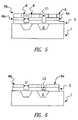
- FIG. 1Shown best in FIG. 1 is a semiconductor substrate 1 including an isolation region 2 that is for example oxide.
- This regionis provided in the semiconductor substrate 1 as shown, or is formed thereon as an insulative layer, for example.
- a conductive layer 3for example of polycrystalline silicon, a first protective layer 4 , for example of silicon nitride, and a second protective layer 5 , for example of oxide, are formed on the semiconductor substrate 1 in this order.
- the conductive layer 3 and second protective layer 5are highly selectively etchable to each other, whereas the selectivity of the first protective layer 4 lies in between.
- a photoresist layer 6is then deposited onto the second protective layer 5 .
- the photoresist layer 6is exposed and developed to uncover portions of the second protective layer 5 having a width A.
- Lines 5 aare defined by plasma etching in the second protective layer 5 , which are mutually separated by first openings 10 , having a width equal to the first width A.
- the photoresist layer 6is then removed as shown in FIG. 2 .
- spacers 8are formed inside the first openings 10 .
- these spacers 8are formed by first depositing a third protective layer 7 , e.g. of the same material as the second protective layer 5 , having a thickness B as shown in FIG. 3 .
- Spacers 8 of a protective materialcan be defined by a plasma etch.
- the width of the second openings 11can be adjusted to far less than is allowed by conventional lithographic techniques.
- the first mask 5 b of this inventionis then used as a screen to fully etch and remove the first protective layer 4 aligned with of the openings 11 , and partly remove the conductive layer 3 to leave it formed with grooves 13 , as shown in FIG. 5 .
- the first mask 5 bis removed by using conventional techniques like wet etching.
- the conductive layer 3is not completely removed by the previous partial etch, so that it will be protecting the isolation regions 2 provided on the substrate 1 that otherwise would be damaged by the step of removing the first protective layer 4 .
- the first protective layer 4there are defined lines 4 a at spacings of C as shown in FIG. 6 .
- the lines 4 aform a second mask 4 b.
- the layer 3 etching stepis completed.
- the conductive layer 3has a plurality of conductive lines 3 a patterned thereon.
- the second mask 4 bcomprises a material that is highly selective to the material of the isolation regions 2 .
- the isolation regions 2 provided on the substrate 1are safeguarded during the final etching of the conductive layer 3 as shown in FIG. 7 .
- the process for defining closely spaced conductive lines 3 a according to the inventionis then completed with removing the first mask 4 b that is selective to both the conductive layer 3 and the isolation regions 2 , as shown in FIG. 8 .
- FIGS. 9 and 10illustrate a modified embodiment of the manufacturing method according to this invention.
- a conductive layer 3 , a first protective layer 4 and a second layer 5are formed on the semiconductor substrate 1 .
- the second protective layer 5is subjected to a polymerizing plasma etching step whereby openings 12 , having sloping sidewalls, are formed as shown in FIG. 9 .
- a mask 5 bis thus provided, wherein the vertical cross-section width of the opening 12 is not constant and decreases in a direction toward the first protective layer 4 . Accordingly, the section of these openings 12 will pass from a first width A to a second width C, that is smaller than the first, close to the protective layer. This because the polymerizing etching step results in spacers 8 a being formed within the opening 12 to provide it with flared sidewalls.
- These spacers 8 aare formed from the polymer material that is present in the polymerizing plasma employed to make the openings 12 .
- the methodcomprises using a double mask, comprising first and second overlaid masks 5 b and 4 b that are employed to pattern a conductive layer 3 on which they have been formed.
- the first protective mask 5 bmade from a layer of an insulating material (e.g., silicon oxide), is formed with openings 11 , 12 to uncover portions of the underlying layer which are smaller than those allowed by conventional photolithographic techniques.
- the first mask 5 bis employed to carry out an etching step of the second mask 4 b beneath and a step of partly etching the conductive layer 3 .
- the second mask 4 bis made from a material of intermediate selectivity in comparison with the layers 5 and 3 in which it is formed.
- the first mask 5 bis then removed.
- the isolation regions 2are undamaged by the removal of the first mask 5 b because they are protected by the layer 3 of conductive material having only been removed in part by the previous etching step.
- the second mask 4 bis subsequently employed to just etch away the conductive layer 3 left over.
- the thickness of the remaining conductive layer 3can be controlled as desired such that a etch of high mask-to-layer selectivity will have no effect on the vertical opening profiles in the layer 3 of conductive material.
- the above-described methodsuits especially the patterning of gate structures of a memory or transistors to provide a dimension pitch that is smaller than that defined by conventional photolithographic techniques.
- a double mask of an insulating materialin particular a dielectric material
- a relatively simple and controllable processcan be developed in order to define sub-lithographic pitches which will safeguard isolation structures previously formed in the wafer, such as interfacing oxides, isolation regions of the LOCOS and STI types, or any being defined.
Landscapes
- Engineering & Computer Science (AREA)
- Physics & Mathematics (AREA)
- Condensed Matter Physics & Semiconductors (AREA)
- General Physics & Mathematics (AREA)
- Manufacturing & Machinery (AREA)
- Computer Hardware Design (AREA)
- Microelectronics & Electronic Packaging (AREA)
- Power Engineering (AREA)
- Chemical & Material Sciences (AREA)
- Inorganic Chemistry (AREA)
- Internal Circuitry In Semiconductor Integrated Circuit Devices (AREA)
Abstract
Description
Claims (36)
Applications Claiming Priority (2)
| Application Number | Priority Date | Filing Date | Title |
|---|---|---|---|
| EP02425505.1AEP1387395B1 (en) | 2002-07-31 | 2002-07-31 | Method for manufacturing semiconductor integrated circuit structures |
| EP02425505.1 | 2002-07-31 |
Publications (2)
| Publication Number | Publication Date |
|---|---|
| US20040132292A1 US20040132292A1 (en) | 2004-07-08 |
| US7163898B2true US7163898B2 (en) | 2007-01-16 |
Family
ID=30011322
Family Applications (1)
| Application Number | Title | Priority Date | Filing Date |
|---|---|---|---|
| US10/631,463Expired - LifetimeUS7163898B2 (en) | 2002-07-31 | 2003-07-30 | Method for manufacturing semiconductor integrated circuit structures |
Country Status (2)
| Country | Link |
|---|---|
| US (1) | US7163898B2 (en) |
| EP (1) | EP1387395B1 (en) |
Cited By (14)
| Publication number | Priority date | Publication date | Assignee | Title |
|---|---|---|---|---|
| US20070262389A1 (en)* | 2004-01-16 | 2007-11-15 | Robert Chau | Tri-gate transistors and methods to fabricate same |
| US20080258207A1 (en)* | 2005-06-30 | 2008-10-23 | Marko Radosavljevic | Block Contact Architectures for Nanoscale Channel Transistors |
| US20110062520A1 (en)* | 2005-06-15 | 2011-03-17 | Brask Justin K | Method for fabricating transistor with thinned channel |
| US20110156145A1 (en)* | 2004-09-29 | 2011-06-30 | Marko Radosavljevic | Fabrication of channel wraparound gate structure for field-effect transistor |
| US20110180851A1 (en)* | 2005-09-28 | 2011-07-28 | Doyle Brian S | Cmos devices with a single work function gate electrode and method of fabrication |
| US7989280B2 (en) | 2005-11-30 | 2011-08-02 | Intel Corporation | Dielectric interface for group III-V semiconductor device |
| US8071983B2 (en) | 2005-06-21 | 2011-12-06 | Intel Corporation | Semiconductor device structures and methods of forming semiconductor structures |
| US8084818B2 (en) | 2004-06-30 | 2011-12-27 | Intel Corporation | High mobility tri-gate devices and methods of fabrication |
| US8183646B2 (en) | 2005-02-23 | 2012-05-22 | Intel Corporation | Field effect transistor with narrow bandgap source and drain regions and method of fabrication |
| US8273626B2 (en) | 2003-06-27 | 2012-09-25 | Intel Corporationn | Nonplanar semiconductor device with partially or fully wrapped around gate electrode and methods of fabrication |
| US8362566B2 (en) | 2008-06-23 | 2013-01-29 | Intel Corporation | Stress in trigate devices using complimentary gate fill materials |
| US8502351B2 (en) | 2004-10-25 | 2013-08-06 | Intel Corporation | Nonplanar device with thinned lower body portion and method of fabrication |
| US8617945B2 (en) | 2006-08-02 | 2013-12-31 | Intel Corporation | Stacking fault and twin blocking barrier for integrating III-V on Si |
| US20150332932A1 (en)* | 2014-05-14 | 2015-11-19 | Tokyo Electron Limited | Method for etching etching target layer |
Families Citing this family (8)
| Publication number | Priority date | Publication date | Assignee | Title |
|---|---|---|---|---|
| ITMI20022785A1 (en) | 2002-12-30 | 2004-06-30 | St Microelectronics Srl | PROCESS FOR THE MANUFACTURE OF MEMORY CELLS |
| ITMI20022784A1 (en) | 2002-12-30 | 2004-06-30 | St Microelectronics Srl | PROCESS FOR THE MANUFACTURE OF MEMORY CELLS |
| US7985687B1 (en)* | 2005-07-22 | 2011-07-26 | Advanced Micro Devices, Inc. | System and method for improving reliability in a semiconductor device |
| US9337261B2 (en)* | 2013-04-10 | 2016-05-10 | GlobalFoundries, Inc. | Method of forming microelectronic or micromechanical structures |
| US20140363963A1 (en)* | 2013-06-07 | 2014-12-11 | Kabushiki Kaisha Toshiba | Method of manufacturing semiconductor device |
| CN108369899B (en)* | 2015-11-20 | 2023-11-17 | 东京毅力科创株式会社 | Method of forming an etch mask for sub-resolution substrate patterning |
| US10068912B1 (en)* | 2017-06-05 | 2018-09-04 | Cypress Semiconductor Corporation | Method of reducing charge loss in non-volatile memories |
| US10566194B2 (en)* | 2018-05-07 | 2020-02-18 | Lam Research Corporation | Selective deposition of etch-stop layer for enhanced patterning |
Citations (7)
| Publication number | Priority date | Publication date | Assignee | Title |
|---|---|---|---|---|
| US5358893A (en)* | 1993-06-10 | 1994-10-25 | Samsung Electronics Co., Ltd. | Isolation method for semiconductor device |
| US5893748A (en) | 1997-02-10 | 1999-04-13 | Advanced Micro Devices, Inc. | Method for producing semiconductor devices with small contacts, vias, or damascene trenches |
| US5998287A (en)* | 1994-06-13 | 1999-12-07 | United Microelectronics Corp. | Process for producing very narrow buried bit lines for non-volatile memory devices |
| US6242795B1 (en) | 1997-10-08 | 2001-06-05 | Winbond Electronics Corp. | Metal line structure and method of manufacturing the same |
| US20010015454A1 (en)* | 1999-12-13 | 2001-08-23 | Samsung Electronics Co., Ltd | Nonvolatile semiconductor memory device and manufacturing method thereof |
| US20010041309A1 (en) | 1999-02-04 | 2001-11-15 | Applied Materials, Inc. | Construction of built-up structures on the surface of patterned masking used for polysilicon etch |
| US6670260B1 (en)* | 1998-11-06 | 2003-12-30 | Advanced Micro Devices, Inc. | Transistor with local insulator structure |
- 2002
- 2002-07-31EPEP02425505.1Apatent/EP1387395B1/ennot_activeExpired - Lifetime
- 2003
- 2003-07-30USUS10/631,463patent/US7163898B2/ennot_activeExpired - Lifetime
Patent Citations (7)
| Publication number | Priority date | Publication date | Assignee | Title |
|---|---|---|---|---|
| US5358893A (en)* | 1993-06-10 | 1994-10-25 | Samsung Electronics Co., Ltd. | Isolation method for semiconductor device |
| US5998287A (en)* | 1994-06-13 | 1999-12-07 | United Microelectronics Corp. | Process for producing very narrow buried bit lines for non-volatile memory devices |
| US5893748A (en) | 1997-02-10 | 1999-04-13 | Advanced Micro Devices, Inc. | Method for producing semiconductor devices with small contacts, vias, or damascene trenches |
| US6242795B1 (en) | 1997-10-08 | 2001-06-05 | Winbond Electronics Corp. | Metal line structure and method of manufacturing the same |
| US6670260B1 (en)* | 1998-11-06 | 2003-12-30 | Advanced Micro Devices, Inc. | Transistor with local insulator structure |
| US20010041309A1 (en) | 1999-02-04 | 2001-11-15 | Applied Materials, Inc. | Construction of built-up structures on the surface of patterned masking used for polysilicon etch |
| US20010015454A1 (en)* | 1999-12-13 | 2001-08-23 | Samsung Electronics Co., Ltd | Nonvolatile semiconductor memory device and manufacturing method thereof |
Cited By (40)
| Publication number | Priority date | Publication date | Assignee | Title |
|---|---|---|---|---|
| US8273626B2 (en) | 2003-06-27 | 2012-09-25 | Intel Corporationn | Nonplanar semiconductor device with partially or fully wrapped around gate electrode and methods of fabrication |
| US20070262389A1 (en)* | 2004-01-16 | 2007-11-15 | Robert Chau | Tri-gate transistors and methods to fabricate same |
| US8084818B2 (en) | 2004-06-30 | 2011-12-27 | Intel Corporation | High mobility tri-gate devices and methods of fabrication |
| US20110156145A1 (en)* | 2004-09-29 | 2011-06-30 | Marko Radosavljevic | Fabrication of channel wraparound gate structure for field-effect transistor |
| US10236356B2 (en) | 2004-10-25 | 2019-03-19 | Intel Corporation | Nonplanar device with thinned lower body portion and method of fabrication |
| US9741809B2 (en) | 2004-10-25 | 2017-08-22 | Intel Corporation | Nonplanar device with thinned lower body portion and method of fabrication |
| US9190518B2 (en) | 2004-10-25 | 2015-11-17 | Intel Corporation | Nonplanar device with thinned lower body portion and method of fabrication |
| US8749026B2 (en) | 2004-10-25 | 2014-06-10 | Intel Corporation | Nonplanar device with thinned lower body portion and method of fabrication |
| US8502351B2 (en) | 2004-10-25 | 2013-08-06 | Intel Corporation | Nonplanar device with thinned lower body portion and method of fabrication |
| US8816394B2 (en) | 2005-02-23 | 2014-08-26 | Intel Corporation | Field effect transistor with narrow bandgap source and drain regions and method of fabrication |
| US9614083B2 (en) | 2005-02-23 | 2017-04-04 | Intel Corporation | Field effect transistor with narrow bandgap source and drain regions and method of fabrication |
| US10121897B2 (en) | 2005-02-23 | 2018-11-06 | Intel Corporation | Field effect transistor with narrow bandgap source and drain regions and method of fabrication |
| US9748391B2 (en) | 2005-02-23 | 2017-08-29 | Intel Corporation | Field effect transistor with narrow bandgap source and drain regions and method of fabrication |
| US8368135B2 (en) | 2005-02-23 | 2013-02-05 | Intel Corporation | Field effect transistor with narrow bandgap source and drain regions and method of fabrication |
| US8183646B2 (en) | 2005-02-23 | 2012-05-22 | Intel Corporation | Field effect transistor with narrow bandgap source and drain regions and method of fabrication |
| US9368583B2 (en) | 2005-02-23 | 2016-06-14 | Intel Corporation | Field effect transistor with narrow bandgap source and drain regions and method of fabrication |
| US9048314B2 (en) | 2005-02-23 | 2015-06-02 | Intel Corporation | Field effect transistor with narrow bandgap source and drain regions and method of fabrication |
| US8664694B2 (en) | 2005-02-23 | 2014-03-04 | Intel Corporation | Field effect transistor with narrow bandgap source and drain regions and method of fabrication |
| US20110062520A1 (en)* | 2005-06-15 | 2011-03-17 | Brask Justin K | Method for fabricating transistor with thinned channel |
| US11978799B2 (en) | 2005-06-15 | 2024-05-07 | Tahoe Research, Ltd. | Method for fabricating transistor with thinned channel |
| US9806195B2 (en) | 2005-06-15 | 2017-10-31 | Intel Corporation | Method for fabricating transistor with thinned channel |
| US9337307B2 (en) | 2005-06-15 | 2016-05-10 | Intel Corporation | Method for fabricating transistor with thinned channel |
| US9385180B2 (en) | 2005-06-21 | 2016-07-05 | Intel Corporation | Semiconductor device structures and methods of forming semiconductor structures |
| US8071983B2 (en) | 2005-06-21 | 2011-12-06 | Intel Corporation | Semiconductor device structures and methods of forming semiconductor structures |
| US9761724B2 (en) | 2005-06-21 | 2017-09-12 | Intel Corporation | Semiconductor device structures and methods of forming semiconductor structures |
| US8581258B2 (en) | 2005-06-21 | 2013-11-12 | Intel Corporation | Semiconductor device structures and methods of forming semiconductor structures |
| US8933458B2 (en) | 2005-06-21 | 2015-01-13 | Intel Corporation | Semiconductor device structures and methods of forming semiconductor structures |
| US20080258207A1 (en)* | 2005-06-30 | 2008-10-23 | Marko Radosavljevic | Block Contact Architectures for Nanoscale Channel Transistors |
| US7898041B2 (en)* | 2005-06-30 | 2011-03-01 | Intel Corporation | Block contact architectures for nanoscale channel transistors |
| US20110180851A1 (en)* | 2005-09-28 | 2011-07-28 | Doyle Brian S | Cmos devices with a single work function gate electrode and method of fabrication |
| US8294180B2 (en) | 2005-09-28 | 2012-10-23 | Intel Corporation | CMOS devices with a single work function gate electrode and method of fabrication |
| US7989280B2 (en) | 2005-11-30 | 2011-08-02 | Intel Corporation | Dielectric interface for group III-V semiconductor device |
| US8617945B2 (en) | 2006-08-02 | 2013-12-31 | Intel Corporation | Stacking fault and twin blocking barrier for integrating III-V on Si |
| US8362566B2 (en) | 2008-06-23 | 2013-01-29 | Intel Corporation | Stress in trigate devices using complimentary gate fill materials |
| US9224754B2 (en) | 2008-06-23 | 2015-12-29 | Intel Corporation | Stress in trigate devices using complimentary gate fill materials |
| US9806193B2 (en) | 2008-06-23 | 2017-10-31 | Intel Corporation | Stress in trigate devices using complimentary gate fill materials |
| US9450092B2 (en) | 2008-06-23 | 2016-09-20 | Intel Corporation | Stress in trigate devices using complimentary gate fill materials |
| US8741733B2 (en) | 2008-06-23 | 2014-06-03 | Intel Corporation | Stress in trigate devices using complimentary gate fill materials |
| US20150332932A1 (en)* | 2014-05-14 | 2015-11-19 | Tokyo Electron Limited | Method for etching etching target layer |
| US9418863B2 (en)* | 2014-05-14 | 2016-08-16 | Tokyo Electron Limited | Method for etching etching target layer |
Also Published As
| Publication number | Publication date |
|---|---|
| EP1387395A1 (en) | 2004-02-04 |
| EP1387395B1 (en) | 2016-11-23 |
| US20040132292A1 (en) | 2004-07-08 |
Similar Documents
| Publication | Publication Date | Title |
|---|---|---|
| US7163898B2 (en) | Method for manufacturing semiconductor integrated circuit structures | |
| US6579757B2 (en) | Method for fabricating semiconductor device which prevents gates of a peripheral region from being oxidized | |
| US6773998B1 (en) | Modified film stack and patterning strategy for stress compensation and prevention of pattern distortion in amorphous carbon gate patterning | |
| US6716761B2 (en) | Method of forming fine patterns | |
| US5667940A (en) | Process for creating high density integrated circuits utilizing double coating photoresist mask | |
| CN100583390C (en) | Method of forming micro pattern in semiconductor device | |
| CN110739210A (en) | Semiconductor structure and forming method thereof | |
| US6596609B2 (en) | Method of fabricating a feature in an integrated circuit using two edge definition layers and a spacer | |
| US7084071B1 (en) | Use of multilayer amorphous carbon ARC stack to eliminate line warpage phenomenon | |
| KR100190261B1 (en) | Method of fabricating gate stack having a reduced height | |
| US20090068842A1 (en) | Method for forming micropatterns in semiconductor device | |
| US6989332B1 (en) | Ion implantation to modulate amorphous carbon stress | |
| US6849530B2 (en) | Method for semiconductor gate line dimension reduction | |
| CN101320712B (en) | Manufacturing method of semiconductor device | |
| US7186614B2 (en) | Method for manufacturing high density flash memory and high performance logic on a single die | |
| KR20070113604A (en) | Method of forming fine pattern of semiconductor device | |
| US6828198B2 (en) | System-on-chip (SOC) solutions with multiple devices by multiple poly gate trimming process | |
| KR20050070320A (en) | Method for forming gate electrode in semiconductor device | |
| US7125775B1 (en) | Method for forming hybrid device gates | |
| US6828082B2 (en) | Method to pattern small features by using a re-flowable hard mask | |
| US7268066B2 (en) | Method for semiconductor gate line dimension reduction | |
| US6812077B1 (en) | Method for patterning narrow gate lines | |
| KR20090001080A (en) | Method of forming fine pattern of semiconductor device | |
| KR100257770B1 (en) | Fine conductive film pattern formation method of semiconductor device | |
| TW502335B (en) | Method for controlling the line width of polysilicon gate by an etching process of a hard mask layer |
Legal Events
| Date | Code | Title | Description |
|---|---|---|---|
| AS | Assignment | Owner name:STMICROELECTRONICS S.R.L., ITALY Free format text:ASSIGNMENT OF ASSIGNORS INTEREST;ASSIGNORS:MARIANI, MARCELLO;BEGHIN, LORENA;REEL/FRAME:014287/0531 Effective date:20040107 | |
| FEPP | Fee payment procedure | Free format text:PAYOR NUMBER ASSIGNED (ORIGINAL EVENT CODE: ASPN); ENTITY STATUS OF PATENT OWNER: LARGE ENTITY | |
| STCF | Information on status: patent grant | Free format text:PATENTED CASE | |
| FPAY | Fee payment | Year of fee payment:4 | |
| AS | Assignment | Owner name:MICRON TECHNOLOGY, INC., IDAHO Free format text:ASSIGNMENT OF ASSIGNORS INTEREST;ASSIGNOR:NUMONYX B.V.;REEL/FRAME:027075/0682 Effective date:20110930 | |
| FEPP | Fee payment procedure | Free format text:PAYER NUMBER DE-ASSIGNED (ORIGINAL EVENT CODE: RMPN); ENTITY STATUS OF PATENT OWNER: LARGE ENTITY Free format text:PAYOR NUMBER ASSIGNED (ORIGINAL EVENT CODE: ASPN); ENTITY STATUS OF PATENT OWNER: LARGE ENTITY | |
| AS | Assignment | Owner name:NUMONYX BV, SWITZERLAND Free format text:ASSIGNMENT OF ASSIGNORS INTEREST;ASSIGNOR:STMICROELECTRONICS NV;REEL/FRAME:032148/0068 Effective date:20120425 Owner name:STMICROELECTRONICS NV, SWITZERLAND Free format text:ASSIGNMENT OF ASSIGNORS INTEREST;ASSIGNOR:STMICROELECTRONICS S.R.L.;REEL/FRAME:032146/0367 Effective date:20080206 | |
| FPAY | Fee payment | Year of fee payment:8 | |
| AS | Assignment | Owner name:U.S. BANK NATIONAL ASSOCIATION, AS COLLATERAL AGENT, CALIFORNIA Free format text:SECURITY INTEREST;ASSIGNOR:MICRON TECHNOLOGY, INC.;REEL/FRAME:038669/0001 Effective date:20160426 Owner name:U.S. BANK NATIONAL ASSOCIATION, AS COLLATERAL AGEN Free format text:SECURITY INTEREST;ASSIGNOR:MICRON TECHNOLOGY, INC.;REEL/FRAME:038669/0001 Effective date:20160426 | |
| AS | Assignment | Owner name:MORGAN STANLEY SENIOR FUNDING, INC., AS COLLATERAL AGENT, MARYLAND Free format text:PATENT SECURITY AGREEMENT;ASSIGNOR:MICRON TECHNOLOGY, INC.;REEL/FRAME:038954/0001 Effective date:20160426 Owner name:MORGAN STANLEY SENIOR FUNDING, INC., AS COLLATERAL Free format text:PATENT SECURITY AGREEMENT;ASSIGNOR:MICRON TECHNOLOGY, INC.;REEL/FRAME:038954/0001 Effective date:20160426 | |
| AS | Assignment | Owner name:U.S. BANK NATIONAL ASSOCIATION, AS COLLATERAL AGENT, CALIFORNIA Free format text:CORRECTIVE ASSIGNMENT TO CORRECT THE REPLACE ERRONEOUSLY FILED PATENT #7358718 WITH THE CORRECT PATENT #7358178 PREVIOUSLY RECORDED ON REEL 038669 FRAME 0001. ASSIGNOR(S) HEREBY CONFIRMS THE SECURITY INTEREST;ASSIGNOR:MICRON TECHNOLOGY, INC.;REEL/FRAME:043079/0001 Effective date:20160426 Owner name:U.S. BANK NATIONAL ASSOCIATION, AS COLLATERAL AGEN Free format text:CORRECTIVE ASSIGNMENT TO CORRECT THE REPLACE ERRONEOUSLY FILED PATENT #7358718 WITH THE CORRECT PATENT #7358178 PREVIOUSLY RECORDED ON REEL 038669 FRAME 0001. ASSIGNOR(S) HEREBY CONFIRMS THE SECURITY INTEREST;ASSIGNOR:MICRON TECHNOLOGY, INC.;REEL/FRAME:043079/0001 Effective date:20160426 | |
| MAFP | Maintenance fee payment | Free format text:PAYMENT OF MAINTENANCE FEE, 12TH YEAR, LARGE ENTITY (ORIGINAL EVENT CODE: M1553) Year of fee payment:12 | |
| AS | Assignment | Owner name:JPMORGAN CHASE BANK, N.A., AS COLLATERAL AGENT, ILLINOIS Free format text:SECURITY INTEREST;ASSIGNORS:MICRON TECHNOLOGY, INC.;MICRON SEMICONDUCTOR PRODUCTS, INC.;REEL/FRAME:047540/0001 Effective date:20180703 Owner name:JPMORGAN CHASE BANK, N.A., AS COLLATERAL AGENT, IL Free format text:SECURITY INTEREST;ASSIGNORS:MICRON TECHNOLOGY, INC.;MICRON SEMICONDUCTOR PRODUCTS, INC.;REEL/FRAME:047540/0001 Effective date:20180703 | |
| AS | Assignment | Owner name:MICRON TECHNOLOGY, INC., IDAHO Free format text:RELEASE BY SECURED PARTY;ASSIGNOR:U.S. BANK NATIONAL ASSOCIATION, AS COLLATERAL AGENT;REEL/FRAME:047243/0001 Effective date:20180629 | |
| AS | Assignment | Owner name:MICRON TECHNOLOGY, INC., IDAHO Free format text:RELEASE BY SECURED PARTY;ASSIGNOR:MORGAN STANLEY SENIOR FUNDING, INC., AS COLLATERAL AGENT;REEL/FRAME:050937/0001 Effective date:20190731 | |
| AS | Assignment | Owner name:MICRON SEMICONDUCTOR PRODUCTS, INC., IDAHO Free format text:RELEASE BY SECURED PARTY;ASSIGNOR:JPMORGAN CHASE BANK, N.A., AS COLLATERAL AGENT;REEL/FRAME:051028/0001 Effective date:20190731 Owner name:MICRON TECHNOLOGY, INC., IDAHO Free format text:RELEASE BY SECURED PARTY;ASSIGNOR:JPMORGAN CHASE BANK, N.A., AS COLLATERAL AGENT;REEL/FRAME:051028/0001 Effective date:20190731 |