US7160805B1 - Inter-layer interconnection structure for large electrical connections - Google Patents
Inter-layer interconnection structure for large electrical connectionsDownload PDFInfo
- Publication number
- US7160805B1 US7160805B1US10/623,082US62308203AUS7160805B1US 7160805 B1US7160805 B1US 7160805B1US 62308203 AUS62308203 AUS 62308203AUS 7160805 B1US7160805 B1US 7160805B1
- Authority
- US
- United States
- Prior art keywords
- elongate
- layer
- copper
- forming
- pad layer
- Prior art date
- Legal status (The legal status is an assumption and is not a legal conclusion. Google has not performed a legal analysis and makes no representation as to the accuracy of the status listed.)
- Expired - Lifetime, expires
Links
Images


Classifications
- H—ELECTRICITY
- H01—ELECTRIC ELEMENTS
- H01L—SEMICONDUCTOR DEVICES NOT COVERED BY CLASS H10
- H01L23/00—Details of semiconductor or other solid state devices
- H01L23/52—Arrangements for conducting electric current within the device in operation from one component to another, i.e. interconnections, e.g. wires, lead frames
- H01L23/522—Arrangements for conducting electric current within the device in operation from one component to another, i.e. interconnections, e.g. wires, lead frames including external interconnections consisting of a multilayer structure of conductive and insulating layers inseparably formed on the semiconductor body
- H01L23/5226—Via connections in a multilevel interconnection structure
- H—ELECTRICITY
- H01—ELECTRIC ELEMENTS
- H01L—SEMICONDUCTOR DEVICES NOT COVERED BY CLASS H10
- H01L23/00—Details of semiconductor or other solid state devices
- H01L23/52—Arrangements for conducting electric current within the device in operation from one component to another, i.e. interconnections, e.g. wires, lead frames
- H01L23/522—Arrangements for conducting electric current within the device in operation from one component to another, i.e. interconnections, e.g. wires, lead frames including external interconnections consisting of a multilayer structure of conductive and insulating layers inseparably formed on the semiconductor body
- H01L23/532—Arrangements for conducting electric current within the device in operation from one component to another, i.e. interconnections, e.g. wires, lead frames including external interconnections consisting of a multilayer structure of conductive and insulating layers inseparably formed on the semiconductor body characterised by the materials
- H01L23/53204—Conductive materials
- H01L23/53209—Conductive materials based on metals, e.g. alloys, metal silicides
- H01L23/53228—Conductive materials based on metals, e.g. alloys, metal silicides the principal metal being copper
- H01L23/53238—Additional layers associated with copper layers, e.g. adhesion, barrier, cladding layers
- H—ELECTRICITY
- H01—ELECTRIC ELEMENTS
- H01L—SEMICONDUCTOR DEVICES NOT COVERED BY CLASS H10
- H01L2924/00—Indexing scheme for arrangements or methods for connecting or disconnecting semiconductor or solid-state bodies as covered by H01L24/00
- H01L2924/0001—Technical content checked by a classifier
- H01L2924/0002—Not covered by any one of groups H01L24/00, H01L24/00 and H01L2224/00
Definitions
- the invention described hereinrelates generally to electrical interconnections in semiconductor devices.
- the inventionrelates to an improved electrical interconnection for large bond pads, bus lines, and other large or wide electrical connections.
- the inventionalso addresses methods for forming such interconnections.
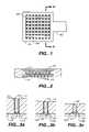
- FIG. 1is a schematic top down representation of one such structure as conventionally known in the art.
- a copper bond pad 101is formed on a semiconductor substrate and electrically connected to a current line 102 .
- the bond pad 101is connected to a complementary bond pad (not shown in this view) formed on an overlying dielectric layer.
- the bond pad 101has a number of slots 103 formed therein.
- the slots 103are stress relief grooves formed in the bond pads 101 . These stress relief grooves segment the larger metal masses into smaller areas, thereby avoiding metal “creep” and other stress related issues. Commonly, these slots 103 pass completely through the bond pads 101 such that the underlying substrate is exposed.
- a dielectric layeris then formed over the bond pads 101 .
- the complementary bond padsare formed in the dielectric layer.
- a multiplicity of dot vias 104are formed in the dielectric layer. These dot vias 104 (called dot vias because of their substantially circular shape) are filled with copper material to provide a conduction path between the bond pad 101 and the overlying complementary bond pad.
- the multiplicity of dot vias 104is often referred to as a sea of vias.
- FIG. 2The cross-section A–A′ is depicted in FIG. 2 which illustrates the conduction paths between the bond pad 101 and the overlying complementary bond pad 111 .
- the slots 103 in the bond pad 101which are now filled with deposited dielectric material, are clearly depicted.
- Side views of sample dot vias 104are well illustrated in this view.
- FIG. 3( a )is a close-up view of the bottom portion of a single representative dot via 104 as it makes an electrical connection with the underlying bond pad 101 .
- the dot via 104is lined with a diffusion barrier 112 and electrically contacts the underlying bond pad 101 through its bottom surface 113 .
- the dot via 104is encapsulated by the surrounding dielectric material 114 . Because copper has a high diffusivity through the dielectric and silicon materials (e.g., dielectric layer 114 ), it is supplied with the barrier layer 112 . This prevents the copper from diffusing into the surrounding dielectric materials and affecting dielectric leakage and potentially causing a host of copper contamination issues.
- FIG. 3( b )illustrates one manifestation of a typical electromigration problem.
- the electrical connection from bottom 104 b of the dot via 104 to the underlying bond pad 101is broken by the formation of a void 120 in the underlying copper bond pad 101 .
- This relatively common occurrenceis precipitated by the electromigration of copper in the bond pad 101 away from the material of the barrier layer 112 .
- the depicted problemis especially troublesome because it causes a complete electrical disconnection between the dot via 104 and the underlying bond pad 101 .
- Such electrical failuresare so prevalent that they are factored in to the final size of the bond pad 101 and the number of dot vias 104 .
- the desired amount of current that must pass through the bond padis determined.
- the number and size of dot vias necessary to carry the currentare calculated, based upon the known dot via failure rates versus current density of vias.
- the predicted number of dot via failuresare then factored in to obtain a final number of vias.
- This final number of viasis then used to determine the size of the bond pad. Therefore, in such conventional approaches, the bond pads are always larger than the minimum possible size.
- the bond padsare made even larger due to the need for the stress relief slots formed in the bond pads. Thus, in existing technologies, excessive surface area is taken up by the overly large electrical connectors (e.g., bond pads).
- FIG. 3( c )depicts another type electromigration problem present in conventional interconnection structures.
- the electrical connection from bottom 104 b of the dot via 104 to the underlying bond pad 101is broken by the formation of a void 121 in the bottom portion of the dot via 104 . This is precipitated by the electromigration of copper in the dot via 104 away from the material of the barrier layer 112 .
- the depicted problemcauses a substantial electrical disconnection between the dot via 104 and the underlying bond pad 101 , thereby choking the amount of current that can pass through the via 104 down to a minimum.
- larger than necessary bond padsare used to address the problem.
- an apparatus and method for fabricating a large electrical interconnection structure for use in semiconductor devicesis disclosed.
- Embodiments of the inventioninclude an electrical interconnection structure for connection to large electrical contacts.
- This electrical interconnectionincludes a semiconductor substrate having a conductive interconnect pad formed thereon.
- a dielectric layer having a plurality of elongate openingsis formed over the conductive interconnect pad.
- the elongate openings of the dielectric layerextend through the dielectric layer to the underlying pad.
- Elongate conductive contactsare formed in the elongate openings to establish electrical connections to the underlying pad.
- the electrical interconnection structureincludes a semiconductor substrate having a copper pad layer formed with a plurality of elongate slots formed therein.
- the slotsextend into the pad layer and have a long axis, a short axis, and sidewalls.
- a dielectric layer having a plurality of elongate bar trenchesoverlies the copper pad. The bar trenches extend through the dielectric layer.
- Elongate conductive contactsare formed in the plurality of elongate openings to establish electrical connections to the underlying copper pad layer. In some embodiments, the elongate conductive contacts are configured to electrically connect to the sidewalls of the copper pads.
- the long axes of the plurality of elongate bar trenchescan be arranged substantially parallel to the long axes of the plurality of the slots formed in the copper pad.
- the long axes of the plurality of elongate bar trenchescan be arranged transversely to the long axes of the plurality of the slots formed in the copper pad.
- FIGS. 1 , 2 , 3 ( a )– 3 ( c )describe conventional approaches and problems in known electrical interconnect structures.
- FIG. 1is a simplified plan view that depicts a conventional bond pad and sea of dot vias.
- FIG. 2is a cross-sectional view that schematically depicts a portion of the electrical interconnection structure shown in FIG. 1 .
- FIG. 3( a )is a schematic cross-sectional view of a dot via constructed in accordance with conventional processes.
- FIG. 3( b )is a schematic cross-sectional view of the dot via depicted in FIG. 3( a ) showing one instance of under-voiding caused by electromigration.
- FIG. 3( c )is another schematic cross-sectional view of the dot via depicted in FIG. 3( a ) showing the formation of a void in the dot via caused by electromigration.
- FIGS. 4( a )– 4 ( d )depict various views of an embodiment of an electrical interconnection structure that include transverse bar contacts formed over the slots of an underlying pad layer in accordance with the principles of the present invention.
- FIGS. 5( a )– 5 ( c )depict various views of an embodiment of an electrical interconnection structure that include bar contacts formed substantially parallel to and over the slots of an underlying pad layer in accordance with the principles of the present invention.
- FIG. 6is a flow diagram describing one embodiment of a suitable method for constructing a electrical interconnect structure in accordance with the principles of the present invention.
- FIG. 4( a )is a schematic top down representation of an electrical interconnect embodiment 400 constructed in accordance with the principles of the present invention.
- a conductive pad layer 402is formed on a semiconductor substrate 401 .
- the conductive pad layer 402is connected to a current line 404 and includes a plurality of slots 403 .
- Overlying the slots 403 and pad layer 402is an elongate bar contact 405 .
- the bar contact 405makes electrical contact with the underlying pad layer 402 .
- Typical embodiments of the elongate bar contact 405have a long dimension in the range of about 0.5–15 ⁇ m with the short dimension of about 5 ⁇ m or less.
- the minimum size of the short dimension of the bar contactis defined by the minimum feature size. In some cases, this can be as small as 0.18 ⁇ m, 0.08 ⁇ m, or even less. In common implementations, the ratio of long dimension to short dimension is about 3:1 or greater. As is known to those having ordinary skill in the art, lower ratios are possible.
- Typical embodimentsutilize a single row of elongate bar contacts 405 to make the electrical connections to the underlying pad layer 402 . The inventors contemplate that, in other embodiments, several rows of elongate bar contacts 405 can be used to make electrical connections to the underlying pad layer 402 .
- the semiconductor substrate 401is a silicon wafer.
- the conductive pad layer 402can comprise bond pads, bus lines, or other wide metal line connections. Such pad layers 402 can be used to form a wide variety of other power distribution nodes or high current lines.
- the pad layers 402can also be used as inter-layer power distribution sites or bond pads for taking power on and off a chip. Pad layers 402 of the present invention can be used to accomplish a wide variety of high current applications. Although depicted here with slots 403 , the inventors contemplate embodiments where pad layers 402 without slots 403 can be used.
- Typical pad layers 402are formed using copper-containing materials (e.g., copper laminate structures, copper alloys, or copper compounds). In the depicted embodiment, the pad layer 402 is simply formed of copper. Such pad layers 402 can be of any size, but preferably range from about 20 ⁇ (micron) ⁇ 20 ⁇ to about 80 ⁇ 80 ⁇ or sometimes larger.
- the depicted pad layer 402includes a number of elongate slots 403 .
- the slots 403are grooves formed in the pad layer 402 to relieve stress. Commonly, these slots 403 pass completely through the pad layer 402 such that the underlying substrate 401 is exposed.
- the elongate openings 430 of the embodimentshave a long axis 431 that extends in the direction parallel to a longer dimension of the elongate opening 430 .
- the elongate openings 430have a short axis 432 that extends in a direction parallel to a shorter axis of the elongate opening 430 .
- a dielectric layer(depicted in other views) is formed over the pad layer 402 .
- elongate openings(or trenches) are formed in the dielectric layer. It is into these trenches that conductive materials are deposited to form the depicted electrical bar contacts 405 .
- the trenchesare configured such that the electrical bar contacts 405 form electrical connections to the underlying pad layer 402 . Methods and techniques of forming these trenches are well known to those having ordinary skill in the art.
- the elongate electrical bar contacts 405are arranged so that the long axes of the contacts 405 are transverse to the long axis of the slots 403 .
- FIG. 4( c )is a cross-sectional view of FIG. 4( a ) taken along line X–X′.
- a pad layer 402is formed on the semiconductor substrate 401 .
- a dielectric layer 407is formed on the pad layer 402 .
- the dielectric layers 407can be formed of a wide range of dielectric materials known to those having ordinary skill in the art.
- a trench 408is formed in the dielectric layer 407 . In one embodiment, the trench 408 is formed by simply selectively etching the dielectric layer 407 to form the depicted trench 408 .
- the trench 408is typically formed such that substrate pad layer 402 is exposed in the slots 403 .
- the underlying substrate 401is also exposed.
- the trench 408exposes the pad layer 402 such that substantial portions of the sidewalls 402 s of the slots 403 are exposed.
- barrier layers 410are typically formed in the trench 408 to prevent subsequently deposited copper materials from diffusing into the dielectric layer 407 .
- Methods of forming such barrier layers 410are known to those having ordinary skill in the art. Typically, refractory metals or refractory metals in combination with other materials are used for barrier layers.
- An electrically conducting contact 411is then formed in the trench 408 .
- the contact 411is formed of copper-containing materials. In the depicted embodiment, the copper-containing material is copper. Methods of forming such contacts are well known to persons having ordinary skill in the art.
- the top of the electrical contacts 411can be planarized, for example, chemical mechanical polishing (CMP) techniques can be used. Additionally, the tops of the electrical contacts 411 can be capped with barrier materials if desired. Techniques and materials similar to those used to form the barrier layers can also be employed. The tops of the electrical contacts 411 can also be electrically connected to other circuit elements if desired.
- CMPchemical mechanical polishing
- the depicted configurationhas substantial advantages over the prior art. For one, electrical contact is now made through the heretofore unused side portions 402 s of the pad layer 402 . This substantially increases the electrical contact area between the electrical contacts 411 and the pad layer 402 . Additionally, because this approach does not lead to open voids from electromigration, this approach offers a much increased electromigration lifetime.
- FIGS. 5( a )– 5 ( c )depict another embodiment of the present invention.
- the elongate trenches formed in the dielectric layerare formed over the elongate slots formed in the underlying conductive pad layer.
- the elongate trenches formed in the dielectric layerare arranged so that the long axes of the elongate trenches are substantially parallel to the long axes of the elongate slots formed in the underlying conductive pad layer.
- Conductive contactsare then formed in the trenches such that they can electrically contact the underlying pad layer.
- FIG. 5( a )is a schematic top down representation of an electrical interconnect embodiment 500 constructed in accordance with the principles of the present invention.
- a conductive pad layer 502is formed on a semiconductor substrate 501 .
- the conductive pad layer 502is connected to a current line 504 and includes a plurality of substantially parallel elongate slots 503 .
- a dielectric layer(not shown in this view) 511 .
- Elongate trenches 508are formed in the dielectric layer. The trenches 508 are formed over the slots 503 .
- both the trenches 508 and the slots 503are substantially parallel. Additionally, the trenches 508 extend through the dielectric layer into the slots 503 such that conducting materials deposited in the trenches 508 will make electrical contact with the underlying pad layer 502 . In some embodiments, the trenches 508 extend into the slots 503 such that conducting materials deposited in the trenches 508 will make electrical contact with sidewalls of the underlying pad layer 502 . Further details of this and other embodiments are explained hereinbelow.
- the semiconductor substrate 501is a silicon wafer. As with the embodiments described hereinabove, the principles of the invention can be practiced using substrates comprising a number of other semiconductor materials.
- the conductive pad layer 502can comprise bond pads, bus lines, or other wide metal line connections as well as a variety of other uses.
- the depicted pad layer 502is formed of copper. However, other conductive materials can be used. As above, pad layers 502 can be of any size, but generally range from about 20 ⁇ (micron) ⁇ 20 ⁇ to about 80 ⁇ 80 ⁇ or sometimes larger.
- FIG. 5( b )is a portion of a cross-section view of the embodiment depicted in FIG. 5( a ) taken along line Y–Y′.
- the pad layer 502is shown formed on the substrate 501 .
- the dielectric layer 511is clearly shown.
- the trenches 508are formed in the dielectric layer 511 in the regions above the slots 503 . As with the foregoing embodiments, it is into these trenches 508 that conductive materials are deposited to form electrical contacts.
- These trenches 508can be formed in a variety of ways as is known to those having ordinary skill in the art. These trenches 508 expose portions of the underlying pad layer 502 .
- the trenches 508can be used to expose the tops 502 T and sidewalls 502 s of the pad layer 502 .
- the trenches 508are configured to expose only the sidewalls 502 s of the pad layer 502 .
- the trenches 508are filled with conductive material to form electrical contacts that form electrical connections to the underlying pad layer 502 .
- the depicted embodimentillustrates a trench arrangement where the trenches 508 are over the slots 503 and also configured so that the long axes of the trenches 508 are substantially parallel to the long axis of the slots 503 .
- a single row of elongate trenches 508(and hence contacts) is formed in the dielectric layer.
- the openings of the trenches 508are wider than the openings for the slots 503 . This exposes a top portion 502 T of the pad layer 502 . For reasons that will be explained later, this has some advantageous features.
- FIG. 5( c )is a cross-sectional depiction of the portion of FIG. 5( b ).
- one or more barrier layers 510can be formed in the trench 508 . As previously explained, this is necessary when copper-containing materials are used. Many well-known techniques for forming such barrier layers 510 can be used.
- An electrically conducting contact 521is then formed in the trench 508 . As above, copper-containing or other conductive materials can be used. In preferred embodiments, copper is used. The methods of forming such contacts 521 are well known to persons having ordinary skill in the art.
- the top of the electrical contacts 521can be planarized or the tops of the electrical contacts 521 can be capped if desired.
- the tops of the electrical contacts 521can also be electrically connected to other circuit elements if desired.
- an electrical conduction pathis now made from the contact 521 through the heretofore unused side portions 502 s of the pad layer 502 .
- this approachcan be used to produce embodiments having an electrical contact area between the contact 521 and the pad layer 502 that has on the order of five (5) times more electrical contact area than for conventional embodiments.
- this approachdoes not lead to open voids from electromigration, this approach offers a much increased electromigration lifetime.
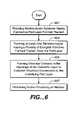
- FIG. 6is a flow diagram illustrating one embodiment of a method for forming an electrical improved interconnection structure for connection to large electrical contacts.
- a semiconductor substrateis provided having a conductive pad layer (Step 601 ).
- the pad layerhas a plurality of elongate slots formed therein.
- the substratecan be a multi-layered structure.
- the substratecan have many layers of semiconductor devices fabricated thereon prior to the implementation of the process of the invention.
- the top layercan also be a dielectric material (e.g., SiO 2 , doped SiO 2 , low-K dielectrics and a list of other materials known to those having ordinary skill in the art).
- the substrateincludes a conductive pad layer formed thereon.
- conductive pad layersare typically formed of copper-containing materials. Examples include copper pad layers, or copper alloy materials, or copper-containing compounds as well as other metals.
- the elongate slotscan be formed as part of the deposition process that forms the pad layer. Alternatively, the slots can be formed as part of a selective etching process. Other processes known to those having ordinary skill in the art can also be employed to form pad layers with elongate slots. The slots themselves are formed to include sidewalls as illustrated in the foregoing embodiments.
- a dielectric layer with a plurality of elongate trenchesis formed over the pad layer (Step 603 ).
- the elongate trenchescan be formed to coincide with the trenches of the pad layer as explained above.
- the elongate trenches of the dielectric layercan be formed to cross transversely over the trenches of the pad layer as explained with respect to FIGS. 4( a )– 4 ( d ).
- These elongate trenchescan be formed in a variety of ways. For example, trench patterns can be formed by selectively depositing a dielectric material such that trenches are formed in the dielectric layer.
- damascene or dual damascene processescan be used to form desired trench patterns (i.e., depositing the dielectric layer over the entire surface, then selectively etching away the dielectric material to obtain the desired trench configuration). In either case, elongate trenches are formed in the dielectric layer. These trenches are formed to expose portions of the underlying pad layer.
- the dielectric layerscan be formed with a wide range of dielectric materials.
- silicon dioxidecan be used.
- combinations of silicon dioxide and other doped dielectricse.g., FSG, BPSG, PSG, etc.
- low-K dielectric materials or other electrically isolating materialsare also used. Examples of such materials include, without limitation, spin-on and CVD polymeric materials based on silicon or carbon, or based on combinations of silicon and carbon. Low-K dielectric materials can also be used.
- examples of such materialsinclude, but are not limited to: organic thermoplastic and thermosetting polymers such as polyimides, polyarylethers, benzocyclo-butenes, polyphenylquinoxalines, polyquinolines; inorganic and spin-on glass materials such as silsesquioxanes, silicates, and siloxanes; and, mixtures, or blends, of organic polymers and spin-on glasses.
- examples of CVD low-K materialsinclude polymers of parylene and napthalene, copolymers of parylene with polysiloxanes or teflon, and polymers of polysiloxane.
- a wide range of proprietary low-K materialsincluding, but not limited to, FLARE (Honeywell Electronic Materials), SiLK (Dow Chemical), or Black Diamond (Applied Materials, Inc.) can be used.
- Electrical contactsare then formed in the openings in the dielectric layer to establish electrical connections to the underlying pad layer (Step 605 ).
- the formation of the electrical connections to the underlying pad layercan be as simple as depositing an appropriate conductive material in the openings of the dielectric layer.
- the conductive materialwill be a copper-containing material.
- barrier materialsare commonly used. Methods and materials for such barrier layers are well known to those having ordinary skill in the art. Typically, refractory metals or refractory metals in combinations of refractory metals with other materials are used in barrier layers.
- Typical examplesinclude, but are not limited to, tungsten (W), tantalum (Ta), and titanium (Ti) based barrier materials (e.g., tantalum nitrides (TaN), tantalum silicon nitrides (TaSiN), tungsten nitrides (WN), and titanium nitrides (TiN)).
- additional barrier materialssuch as Chromium (Cr), Magnesium (Mg), Molybdenum (Mo), or Palladium (Pa), Vanadium (Va) or Tungsten (W) can be used.
- a copper materialcan be used to form the contact.
- a thin seed layer of copperis deposited, for example, using sputter deposition to deposit the seed layer.
- a thick bulk layer of copperis deposited using, for example, electroplating.
- Such further processingcan include surface planarization.
- planarizationcan be accomplished using chemical mechanical polishing (CMP) techniques.
- CMPchemical mechanical polishing
- the tops of the electrical contactscan be capped if desired using similar techniques and materials to those used in the above-disclosed barrier layer.
- the tops of the electrical contactscan also be electrically connected to other circuit elements if desired.
Landscapes
- Physics & Mathematics (AREA)
- Condensed Matter Physics & Semiconductors (AREA)
- General Physics & Mathematics (AREA)
- Engineering & Computer Science (AREA)
- Computer Hardware Design (AREA)
- Microelectronics & Electronic Packaging (AREA)
- Power Engineering (AREA)
- Internal Circuitry In Semiconductor Integrated Circuit Devices (AREA)
Abstract
Description
Claims (13)
Priority Applications (1)
| Application Number | Priority Date | Filing Date | Title |
|---|---|---|---|
| US10/623,082US7160805B1 (en) | 2002-10-16 | 2003-07-17 | Inter-layer interconnection structure for large electrical connections |
Applications Claiming Priority (2)
| Application Number | Priority Date | Filing Date | Title |
|---|---|---|---|
| US10/272,767US6642597B1 (en) | 2002-10-16 | 2002-10-16 | Inter-layer interconnection structure for large electrical connections |
| US10/623,082US7160805B1 (en) | 2002-10-16 | 2003-07-17 | Inter-layer interconnection structure for large electrical connections |
Related Parent Applications (1)
| Application Number | Title | Priority Date | Filing Date |
|---|---|---|---|
| US10/272,767DivisionUS6642597B1 (en) | 2002-10-16 | 2002-10-16 | Inter-layer interconnection structure for large electrical connections |
Publications (1)
| Publication Number | Publication Date |
|---|---|
| US7160805B1true US7160805B1 (en) | 2007-01-09 |
Family
ID=29270323
Family Applications (2)
| Application Number | Title | Priority Date | Filing Date |
|---|---|---|---|
| US10/272,767Expired - LifetimeUS6642597B1 (en) | 2002-10-16 | 2002-10-16 | Inter-layer interconnection structure for large electrical connections |
| US10/623,082Expired - LifetimeUS7160805B1 (en) | 2002-10-16 | 2003-07-17 | Inter-layer interconnection structure for large electrical connections |
Family Applications Before (1)
| Application Number | Title | Priority Date | Filing Date |
|---|---|---|---|
| US10/272,767Expired - LifetimeUS6642597B1 (en) | 2002-10-16 | 2002-10-16 | Inter-layer interconnection structure for large electrical connections |
Country Status (1)
| Country | Link |
|---|---|
| US (2) | US6642597B1 (en) |
Cited By (17)
| Publication number | Priority date | Publication date | Assignee | Title |
|---|---|---|---|---|
| US20070063352A1 (en)* | 2005-09-21 | 2007-03-22 | Agere Systems Inc. | Routing under bond pad for the replacement of an interconnect layer |
| US20070114667A1 (en)* | 2005-11-18 | 2007-05-24 | Lsi Logic Corporation | Alternate pad structures/passivation inegration schemes to reduce or eliminate IMC cracking in post wire bonded dies during Cu/Low-K BEOL processing |
| US20090098687A1 (en)* | 2007-10-10 | 2009-04-16 | Joze Eura Antol | Integrated circuit package including wire bonds |
| US20100032809A1 (en)* | 2008-08-08 | 2010-02-11 | International Business Machines Corporation | Metal wiring structure for integration with through substrate vias |
| US20100201000A1 (en)* | 2007-10-31 | 2010-08-12 | Agere Systems Inc. | Bond pad support structure for semiconductor device |
| US7952206B2 (en) | 2005-09-27 | 2011-05-31 | Agere Systems Inc. | Solder bump structure for flip chip semiconductor devices and method of manufacture therefore |
| US20110215481A1 (en)* | 2005-08-09 | 2011-09-08 | Panasonic Corporation | Semiconductor device |
| US20120132966A1 (en)* | 2007-10-15 | 2012-05-31 | International Business Machines Corporation | Semiconductor structures having improved contact resistance |
| US20130228897A1 (en)* | 2012-03-01 | 2013-09-05 | Taiwan Semiconductor Manufacturing Company, Ltd. | Electrical Connections for Chip Scale Packaging |
| US8640072B1 (en)* | 2012-07-31 | 2014-01-28 | Freescale Semiconductor, Inc. | Method for forming an electrical connection between metal layers |
| US9032615B2 (en) | 2012-07-31 | 2015-05-19 | Freescale Semiconductor, Inc. | Method for forming an electrical connection between metal layers |
| US9087882B2 (en) | 2011-06-03 | 2015-07-21 | Taiwan Semiconductor Manufacturing Company, Ltd. | Electrical connection for chip scale packaging |
| US9123788B2 (en) | 2012-08-17 | 2015-09-01 | Taiwan Semiconductor Manufacturing Company, Ltd. | Bonded structures for package and substrate |
| US9196573B2 (en) | 2012-07-31 | 2015-11-24 | Taiwan Semiconductor Manufacturing Company, Ltd. | Bump on pad (BOP) bonding structure |
| US9548281B2 (en) | 2011-10-07 | 2017-01-17 | Taiwan Semiconductor Manufacturing Company, Ltd. | Electrical connection for chip scale packaging |
| US9673161B2 (en) | 2012-08-17 | 2017-06-06 | Taiwan Semiconductor Manufacturing Company, Ltd. | Bonded structures for package and substrate |
| US20220293542A1 (en)* | 2021-03-10 | 2022-09-15 | Changxin Memory Technologies, Inc. | Semiconductor structure and manufacturing method of semiconductor structure |
Families Citing this family (4)
| Publication number | Priority date | Publication date | Assignee | Title |
|---|---|---|---|---|
| US6828223B2 (en)* | 2001-12-14 | 2004-12-07 | Taiwan Semiconductor Manufacturing Co. | Localized slots for stress relieve in copper |
| JP4068497B2 (en)* | 2003-04-24 | 2008-03-26 | 株式会社東芝 | Semiconductor device and manufacturing method thereof |
| KR20100060309A (en)* | 2008-11-27 | 2010-06-07 | 주식회사 동부하이텍 | A semiconductor device |
| US8569891B1 (en)* | 2010-03-16 | 2013-10-29 | Micron Technology, Inc. | Forming array contacts in semiconductor memories |
Citations (7)
| Publication number | Priority date | Publication date | Assignee | Title |
|---|---|---|---|---|
| JPS58110055A (en)* | 1981-12-23 | 1983-06-30 | Nec Corp | Semiconductor device |
| US5565707A (en)* | 1994-10-31 | 1996-10-15 | International Business Machines Corporation | Interconnect structure using a Al2 Cu for an integrated circuit chip |
| US6197688B1 (en)* | 1998-02-12 | 2001-03-06 | Motorola Inc. | Interconnect structure in a semiconductor device and method of formation |
| US6198170B1 (en)* | 1999-12-16 | 2001-03-06 | Conexant Systems, Inc. | Bonding pad and support structure and method for their fabrication |
| US6313540B1 (en)* | 1998-12-25 | 2001-11-06 | Nec Corporation | Electrode structure of semiconductor element |
| US6313537B1 (en)* | 1997-12-09 | 2001-11-06 | Samsung Electronics Co., Ltd. | Semiconductor device having multi-layered pad and a manufacturing method thereof |
| US6746951B2 (en)* | 2000-10-20 | 2004-06-08 | Samsung Electronics Co., Ltd. | Bond pad of semiconductor device and method of fabricating the same |
- 2002
- 2002-10-16USUS10/272,767patent/US6642597B1/ennot_activeExpired - Lifetime
- 2003
- 2003-07-17USUS10/623,082patent/US7160805B1/ennot_activeExpired - Lifetime
Patent Citations (7)
| Publication number | Priority date | Publication date | Assignee | Title |
|---|---|---|---|---|
| JPS58110055A (en)* | 1981-12-23 | 1983-06-30 | Nec Corp | Semiconductor device |
| US5565707A (en)* | 1994-10-31 | 1996-10-15 | International Business Machines Corporation | Interconnect structure using a Al2 Cu for an integrated circuit chip |
| US6313537B1 (en)* | 1997-12-09 | 2001-11-06 | Samsung Electronics Co., Ltd. | Semiconductor device having multi-layered pad and a manufacturing method thereof |
| US6197688B1 (en)* | 1998-02-12 | 2001-03-06 | Motorola Inc. | Interconnect structure in a semiconductor device and method of formation |
| US6313540B1 (en)* | 1998-12-25 | 2001-11-06 | Nec Corporation | Electrode structure of semiconductor element |
| US6198170B1 (en)* | 1999-12-16 | 2001-03-06 | Conexant Systems, Inc. | Bonding pad and support structure and method for their fabrication |
| US6746951B2 (en)* | 2000-10-20 | 2004-06-08 | Samsung Electronics Co., Ltd. | Bond pad of semiconductor device and method of fabricating the same |
Cited By (41)
| Publication number | Priority date | Publication date | Assignee | Title |
|---|---|---|---|---|
| US20110215481A1 (en)* | 2005-08-09 | 2011-09-08 | Panasonic Corporation | Semiconductor device |
| US8319343B2 (en) | 2005-09-21 | 2012-11-27 | Agere Systems Llc | Routing under bond pad for the replacement of an interconnect layer |
| US20070063352A1 (en)* | 2005-09-21 | 2007-03-22 | Agere Systems Inc. | Routing under bond pad for the replacement of an interconnect layer |
| US7952206B2 (en) | 2005-09-27 | 2011-05-31 | Agere Systems Inc. | Solder bump structure for flip chip semiconductor devices and method of manufacture therefore |
| US8507317B2 (en) | 2005-09-27 | 2013-08-13 | Agere Systems Llc | Solder bump structure for flip chip semiconductor devices and method of manufacturing therefore |
| US8552560B2 (en) | 2005-11-18 | 2013-10-08 | Lsi Corporation | Alternate pad structures/passivation inegration schemes to reduce or eliminate IMC cracking in post wire bonded dies during Cu/Low-K BEOL processing |
| US20070114667A1 (en)* | 2005-11-18 | 2007-05-24 | Lsi Logic Corporation | Alternate pad structures/passivation inegration schemes to reduce or eliminate IMC cracking in post wire bonded dies during Cu/Low-K BEOL processing |
| US7888257B2 (en) | 2007-10-10 | 2011-02-15 | Agere Systems Inc. | Integrated circuit package including wire bonds |
| US20090098687A1 (en)* | 2007-10-10 | 2009-04-16 | Joze Eura Antol | Integrated circuit package including wire bonds |
| US20120208332A1 (en)* | 2007-10-15 | 2012-08-16 | International Business Machines Corporation | Semiconductor structures having improved contact resistance |
| US8685809B2 (en)* | 2007-10-15 | 2014-04-01 | International Business Machines Corporation | Semiconductor structures having improved contact resistance |
| US20120132966A1 (en)* | 2007-10-15 | 2012-05-31 | International Business Machines Corporation | Semiconductor structures having improved contact resistance |
| US8299455B2 (en)* | 2007-10-15 | 2012-10-30 | International Business Machines Corporation | Semiconductor structures having improved contact resistance |
| US8183698B2 (en) | 2007-10-31 | 2012-05-22 | Agere Systems Inc. | Bond pad support structure for semiconductor device |
| US20100201000A1 (en)* | 2007-10-31 | 2010-08-12 | Agere Systems Inc. | Bond pad support structure for semiconductor device |
| US20110185330A1 (en)* | 2008-08-08 | 2011-07-28 | International Business Machines Corporation | Metal wiring structure for integration with through substrate vias |
| US7968975B2 (en) | 2008-08-08 | 2011-06-28 | International Business Machines Corporation | Metal wiring structure for integration with through substrate vias |
| US8234606B2 (en) | 2008-08-08 | 2012-07-31 | International Business Machines Corporation | Metal wiring structure for integration with through substrate vias |
| US20100032809A1 (en)* | 2008-08-08 | 2010-02-11 | International Business Machines Corporation | Metal wiring structure for integration with through substrate vias |
| US9087882B2 (en) | 2011-06-03 | 2015-07-21 | Taiwan Semiconductor Manufacturing Company, Ltd. | Electrical connection for chip scale packaging |
| US9515038B2 (en) | 2011-06-03 | 2016-12-06 | Taiwan Semiconductor Manufacturing Company, Ltd. | Electrical connection for chip scale packaging |
| US9548281B2 (en) | 2011-10-07 | 2017-01-17 | Taiwan Semiconductor Manufacturing Company, Ltd. | Electrical connection for chip scale packaging |
| US9224680B2 (en) | 2011-10-07 | 2015-12-29 | Taiwan Semiconductor Manufacturing Company, Ltd. | Electrical connections for chip scale packaging |
| US9741659B2 (en)* | 2011-10-07 | 2017-08-22 | Taiwan Semiconductor Manufacturing Company, Ltd. | Electrical connections for chip scale packaging |
| US20160111363A1 (en)* | 2011-10-07 | 2016-04-21 | Taiwan Semiconductor Manufacturing Company, Ltd. | Electrical Connections for Chip Scale Packaging |
| US20130228897A1 (en)* | 2012-03-01 | 2013-09-05 | Taiwan Semiconductor Manufacturing Company, Ltd. | Electrical Connections for Chip Scale Packaging |
| US8912668B2 (en)* | 2012-03-01 | 2014-12-16 | Taiwan Semiconductor Manufacturing Company, Ltd. | Electrical connections for chip scale packaging |
| US20140094029A1 (en)* | 2012-07-31 | 2014-04-03 | Freescale Semconductor, Inc. | Method for forming an electrical connection between metal layers |
| US9196573B2 (en) | 2012-07-31 | 2015-11-24 | Taiwan Semiconductor Manufacturing Company, Ltd. | Bump on pad (BOP) bonding structure |
| US9748188B2 (en) | 2012-07-31 | 2017-08-29 | Taiwan Semiconductor Manufacturing Company, Ltd. | Method of forming a bump on pad (BOP) bonding structure in a semiconductor packaged device |
| US10515917B2 (en) | 2012-07-31 | 2019-12-24 | Taiwan Semiconductor Manufacturing Company, Ltd. | Bump on pad (BOP) bonding structure in semiconductor packaged device |
| US8640072B1 (en)* | 2012-07-31 | 2014-01-28 | Freescale Semiconductor, Inc. | Method for forming an electrical connection between metal layers |
| US9032615B2 (en) | 2012-07-31 | 2015-05-19 | Freescale Semiconductor, Inc. | Method for forming an electrical connection between metal layers |
| US10163839B2 (en) | 2012-07-31 | 2018-12-25 | Taiwan Semiconductor Manufacturing Company, Ltd. | Bump on pad (BOP) bonding structure in semiconductor packaged device |
| US8972922B2 (en)* | 2012-07-31 | 2015-03-03 | Freescale Semiconductor, Inc. | Method for forming an electrical connection between metal layers |
| US9123788B2 (en) | 2012-08-17 | 2015-09-01 | Taiwan Semiconductor Manufacturing Company, Ltd. | Bonded structures for package and substrate |
| US9673161B2 (en) | 2012-08-17 | 2017-06-06 | Taiwan Semiconductor Manufacturing Company, Ltd. | Bonded structures for package and substrate |
| US10468366B2 (en) | 2012-08-17 | 2019-11-05 | Taiwan Semiconductor Manufacturing Company, Ltd. | Bonded structures for package and substrate |
| US9397059B2 (en) | 2012-08-17 | 2016-07-19 | Taiwan Semiconductor Manufacturing Company, Ltd. | Bonded structures for package and substrate |
| US11088102B2 (en) | 2012-08-17 | 2021-08-10 | Taiwan Semiconductor Manufacturing Company, Ltd. | Bonded structures for package and substrate |
| US20220293542A1 (en)* | 2021-03-10 | 2022-09-15 | Changxin Memory Technologies, Inc. | Semiconductor structure and manufacturing method of semiconductor structure |
Also Published As
| Publication number | Publication date |
|---|---|
| US6642597B1 (en) | 2003-11-04 |
Similar Documents
| Publication | Publication Date | Title |
|---|---|---|
| US7160805B1 (en) | Inter-layer interconnection structure for large electrical connections | |
| US6509267B1 (en) | Method of forming low resistance barrier on low k interconnect with electrolessly plated copper seed layer | |
| US6468894B1 (en) | Metal interconnection structure with dummy vias | |
| JP4832807B2 (en) | Semiconductor device | |
| US7439624B2 (en) | Enhanced mechanical strength via contacts | |
| US7586175B2 (en) | Semiconductor wafer having embedded electroplating current paths to provide uniform plating over wafer surface | |
| US7569467B2 (en) | Semiconductor device and manufacturing method thereof | |
| JP4852234B2 (en) | Metal wiring structure and metal wiring method in which void generation is prevented | |
| US7902061B2 (en) | Interconnect structures with encasing cap and methods of making thereof | |
| US7514354B2 (en) | Methods for forming damascene wiring structures having line and plug conductors formed from different materials | |
| US6756672B1 (en) | Use of sic for preventing copper contamination of low-k dielectric layers | |
| US20030186535A1 (en) | Method of making semiconductor device using a novel interconnect cladding layer | |
| US6514860B1 (en) | Integration of organic fill for dual damascene process | |
| US8129842B2 (en) | Enhanced interconnect structure | |
| US11062943B2 (en) | Top via interconnects with wrap around liner | |
| US7144761B2 (en) | Semiconductor device and method for fabricating the same | |
| JP4130621B2 (en) | Semiconductor device and manufacturing method thereof | |
| US7312532B2 (en) | Dual damascene interconnect structure with improved electro migration lifetimes | |
| US6448654B1 (en) | Ultra thin etch stop layer for damascene process | |
| US6455938B1 (en) | Integrated circuit interconnect shunt layer | |
| KR100408182B1 (en) | Copper barrier layer for copper layer | |
| US8278758B1 (en) | Multilevel reservoirs for integrated circuit interconnects | |
| US20060180934A1 (en) | Wiring structures for semiconductor devices | |
| KR20070055910A (en) | How to form via contact structures using dual damascene technology | |
| KR20020055310A (en) | Method of manufacturing a metal wiring in a semiconductor device |
Legal Events
| Date | Code | Title | Description |
|---|---|---|---|
| STCF | Information on status: patent grant | Free format text:PATENTED CASE | |
| FEPP | Fee payment procedure | Free format text:PAYOR NUMBER ASSIGNED (ORIGINAL EVENT CODE: ASPN); ENTITY STATUS OF PATENT OWNER: LARGE ENTITY | |
| FPAY | Fee payment | Year of fee payment:4 | |
| FPAY | Fee payment | Year of fee payment:8 | |
| AS | Assignment | Owner name:AVAGO TECHNOLOGIES GENERAL IP (SINGAPORE) PTE. LTD Free format text:ASSIGNMENT OF ASSIGNORS INTEREST;ASSIGNOR:LSI CORPORATION;REEL/FRAME:035058/0248 Effective date:20140804 | |
| AS | Assignment | Owner name:BANK OF AMERICA, N.A., AS COLLATERAL AGENT, NORTH CAROLINA Free format text:PATENT SECURITY AGREEMENT;ASSIGNOR:AVAGO TECHNOLOGIES GENERAL IP (SINGAPORE) PTE. LTD.;REEL/FRAME:037808/0001 Effective date:20160201 Owner name:BANK OF AMERICA, N.A., AS COLLATERAL AGENT, NORTH Free format text:PATENT SECURITY AGREEMENT;ASSIGNOR:AVAGO TECHNOLOGIES GENERAL IP (SINGAPORE) PTE. LTD.;REEL/FRAME:037808/0001 Effective date:20160201 | |
| AS | Assignment | Owner name:AVAGO TECHNOLOGIES GENERAL IP (SINGAPORE) PTE. LTD., SINGAPORE Free format text:TERMINATION AND RELEASE OF SECURITY INTEREST IN PATENTS;ASSIGNOR:BANK OF AMERICA, N.A., AS COLLATERAL AGENT;REEL/FRAME:041710/0001 Effective date:20170119 Owner name:AVAGO TECHNOLOGIES GENERAL IP (SINGAPORE) PTE. LTD Free format text:TERMINATION AND RELEASE OF SECURITY INTEREST IN PATENTS;ASSIGNOR:BANK OF AMERICA, N.A., AS COLLATERAL AGENT;REEL/FRAME:041710/0001 Effective date:20170119 | |
| AS | Assignment | Owner name:BELL SEMICONDUCTOR, LLC, ILLINOIS Free format text:ASSIGNMENT OF ASSIGNORS INTEREST;ASSIGNORS:AVAGO TECHNOLOGIES GENERAL IP (SINGAPORE) PTE. LTD.;BROADCOM CORPORATION;REEL/FRAME:044886/0001 Effective date:20171208 | |
| AS | Assignment | Owner name:CORTLAND CAPITAL MARKET SERVICES LLC, AS COLLATERA Free format text:SECURITY INTEREST;ASSIGNORS:HILCO PATENT ACQUISITION 56, LLC;BELL SEMICONDUCTOR, LLC;BELL NORTHERN RESEARCH, LLC;REEL/FRAME:045216/0020 Effective date:20180124 | |
| MAFP | Maintenance fee payment | Free format text:PAYMENT OF MAINTENANCE FEE, 12TH YEAR, LARGE ENTITY (ORIGINAL EVENT CODE: M1553) Year of fee payment:12 | |
| AS | Assignment | Owner name:BELL NORTHERN RESEARCH, LLC, ILLINOIS Free format text:SECURITY INTEREST;ASSIGNOR:CORTLAND CAPITAL MARKET SERVICES LLC;REEL/FRAME:060885/0001 Effective date:20220401 Owner name:BELL SEMICONDUCTOR, LLC, ILLINOIS Free format text:SECURITY INTEREST;ASSIGNOR:CORTLAND CAPITAL MARKET SERVICES LLC;REEL/FRAME:060885/0001 Effective date:20220401 Owner name:HILCO PATENT ACQUISITION 56, LLC, ILLINOIS Free format text:SECURITY INTEREST;ASSIGNOR:CORTLAND CAPITAL MARKET SERVICES LLC;REEL/FRAME:060885/0001 Effective date:20220401 |