US7160121B2 - Stressed metal contact with enhanced lateral compliance - Google Patents
Stressed metal contact with enhanced lateral complianceDownload PDFInfo
- Publication number
- US7160121B2 US7160121B2US10/737,272US73727203AUS7160121B2US 7160121 B2US7160121 B2US 7160121B2US 73727203 AUS73727203 AUS 73727203AUS 7160121 B2US7160121 B2US 7160121B2
- Authority
- US
- United States
- Prior art keywords
- plane
- interconnect element
- spring
- release portion
- curve
- Prior art date
- Legal status (The legal status is an assumption and is not a legal conclusion. Google has not performed a legal analysis and makes no representation as to the accuracy of the status listed.)
- Expired - Lifetime
Links
Images


Classifications
- H—ELECTRICITY
- H01—ELECTRIC ELEMENTS
- H01R—ELECTRICALLY-CONDUCTIVE CONNECTIONS; STRUCTURAL ASSOCIATIONS OF A PLURALITY OF MUTUALLY-INSULATED ELECTRICAL CONNECTING ELEMENTS; COUPLING DEVICES; CURRENT COLLECTORS
- H01R13/00—Details of coupling devices of the kinds covered by groups H01R12/70 or H01R24/00 - H01R33/00
- H01R13/02—Contact members
- H01R13/22—Contacts for co-operating by abutting
- H01R13/24—Contacts for co-operating by abutting resilient; resiliently-mounted
- H01R13/2407—Contacts for co-operating by abutting resilient; resiliently-mounted characterized by the resilient means
Definitions
- CMOScomplementary metal-oxide-semiconductor
- CMOScomplementary metal-oxide-semiconductor
- CMOScomplementary metal-oxide-semiconductor
- CMOScomplementary metal-oxide-semiconductor
- CMOScomplementary metal-oxide-semiconductor
- J-Shaped spring contactshave been developed as described in U.S. patent application Ser. No. 10/443,957, entitled “Multi-Axis Compliance Spring” based on provisional application No. 60/382,602 filed May 24, 2002.
- the entire document of the patent application and the related provisional applicationare hereby incorporated by referenced in their entirety.
- the disclosed J spring designsoffer improved lateral compliance, the designs use substantial area on an integrated circuit.
- the design of the J springsmake it difficult to route traces around the spring array.
- the contact point that mates with the circuit board padis not the spring tip but rather the J spring outer edge. When the approximately 90 degree point of the outer edge is soldered to the mating board pad, extending the J shape beyond 90° does not provide additional spring compliance.
- the interconnectincludes an anchor portion coupled to a substrate.
- a flexible stressed metal forming a release portionis coupled to the anchor portion.
- the release portionincludes a tip and at least one curve. The curves in the release portion arranged such that the tip is in a desired orientation.
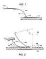
- FIG. 1shows a side view of a stressed metal interconnect.
- FIG. 2shows a shows a side view of an interconnect structure disposed on a substrate.
- FIG. 3shows a side view of a release layer deposited over a substrate.
- FIG. 4shows a stressed metal deposited over the release layer.
- FIG. 5removal of the release layer to create an uplift region.
- FIG. 6shows depositing a highly conducting layer over the interconnect structure to improve conductivity of the interconnect structure
- FIG. 7shows a top view of an interconnect structure including a plurality of curves to enhance lateral compliance.
- FIG. 8shows a top view of one embodiment of an interconnect structure including a release portion that includes an uplift portion and a planar portion.
- FIG. 9shows a top view of a second embodiment of an interconnect structure including a release portion that include an uplift portion and a planar portion.
- FIG. 10shows an angled view of the structure of FIG. 9 with an uplift portion curved out of the plane of the substrate.
- FIG. 11shows a top view of an interconnect structure including a release portion with an aperture.
- FIG. 12shows an angled view of the structure of FIG. 11 that shows a release portion curved out of the plane of the substrate.
- FIG. 13shows a second embodiment of an interconnect structure including an aperture.
- FIG. 14shows an angled view of the structure of FIG. 13 that shows a release portion curved out of the plane of the substrate.
- a structure and method for coupling two electrical elementsuses a stressed metal that includes a release portion that includes. at least one in-plane curve.
- the release portionfurther includes an uplift portion that may coincide with, or be only a part of the release portion. If the uplift portion includes in-plane curves, the total arc subtended by all in-plane curves in the uplift region totals approximately zero degrees. Clockwise bends are counted positive in this total, counter clockwise bends negative.
- in-plane curvesrefer to curves that exist in a lateral direction, usually curves that exist in the plane of the substrate prior to removal of a release layer that allows uplifting of the stressed metal.
- the term “in-plane curve”is used to distinguish from the curvature out of the plane that results from metal stresses.
- In-plane curvesimprove the compliance of the interconnect in a lateral direction reducing the rate of failure among such interconnects when lateral stresses are applied. Keeping the total angle subtended by all in-plane curves in the uplift spring portion to approximately zero degrees helps orient the tip to point away from the substrate. Maintaining a net of 0 degrees of curvature in the uplift portion of the spring also minimizes tip tilt thereby maximizing spring tip contact with the mating circuit board pad. Finally, maintaining a net of 0 degrees curvature in the uplift portion allows the entire spring length to contribute to the spring compliance.
- FIG. 1shows a side view of a stressed metal interconnect 104 used to couple a first circuit element 108 to a second circuit element 112 .
- first circuit element 108is an integrated circuit and second circuit element 112 is a bond pad of printed circuit board.
- solder 116fixes first circuit element 108 to a first end of stressed metal interconnect 104 .
- Mechanical tension generated by a bend 120creates a spring action that fixes a second end of metal interconnect 104 to the bond pad.
- Stressed metal interconnect 104may be formed from a variety of materials. As described in U.S. Pat. No. 5,613,861 entitled Photolithographically Patterened Spring Contacts by Donald Smith and Andrew Alimonda and hereby incorporated by reference in its entirety, most often the stressed metal interconnect 104 is formed from materials such as molybdenum, chromium, tungsten, nickel, zirconium or alloys thereof.
- FIG. 2shows a side view of the interconnect structure 200 having disposed on the substrate 204 .
- interconnect structure 200is either made with a conducting material, or coated or plated with a conductive material. Alternately, interconnect structure 200 may be made with a nonconducting material, and then subsequently coated with a conducting material. A detailed more detailed description of the fabrication of the spring will be provided in the flow chart of FIG. 3 .
- interconnect structure 200has an anchor portion 208 that is fixed to an underlayer 212 and electrically connected to a contact pad 216 .
- underlayer 212is a conductive underlayer made from a material such as titanium or other etchable material.
- the contact pad 216is often made of a metal such as aluminum, gold, indium, tin oxide, copper, silver, nickel or the like.
- FIG. 2shows the interconnect structure in three positions.
- the interconnect structureis formed in positions 220 , where a release portion 224 of interconnect structure 200 attaches to substrate 204 .
- a release portion 224 of interconnect structure 200attaches to substrate 204 .
- internal stressescause release portion 224 to form an out of the substrate plane curve 228 .
- the out of plane curve 228subtends an angle theta.
- the out of plane curve formedis in a plane approximately perpendicular to the surface of substrate 204 .
- a second contact pad 232is brought into contact with release portion 224 .
- Pressure applied by contact pad 232reduces the curvature of interconnect structure 200 .
- Spring pressure or tension in interconnect structure 200maintains electrical contact between contact pad 216 coupled to anchor portion of interconnect structure 200 and contact pad 232 coupled to the release portion 224 of interconnect structure 200 .
- FIGS. 3–6show one method of forming interconnect structure 200 .
- a contact pad 304is formed over or adjacent to a substrate 308 .
- a release layer 312is also deposited over substrate 308 .
- Release layer 312is typically an electrical conductor.
- a stressed metal layer 400is deposited on or over substrate 308 .
- the metalmay be one of a variety of materials, such as a MoCr alloy.
- An anchor portion 414 of metal layer 400couples to anchor pad 304 .
- a release portion 418 of metal layer 400is deposited over release layer 312 .
- Techniques for depositing metal layer 400include, but are not limited to electron beam deposition, thermal evaporation, sputter deposition, electroplating and chemical vapor deposition as well as other techniques.
- Metal layer 400includes a plurality of sublayers 422 , 426 , 430 such that the total plurality of sublayers results in a metal layer 400 approximately 1 micrometer thick.
- a stress gradientis generated in metal layer 400 by altering the stress inherent in each of the sublayers 422 , 426 , 430 as each sublayer is formed.
- There are numerous ways of introducing such stress in the sublayersincluding but not limited to adding a reactive gas to a plasma used during sputter deposition, depositing the metal at an angle, and changing the pressure of the plasma during deposition.
- An example methodsputters a metal in a vacuum chamber.
- metal layer 400As each metal layer is deposited, the pressure within the vacuum chamber is increased causing compressive stress in early deposited layers and tensile stress in later deposited layers. After formation, metal layer 400 has an intrinsic stress that becomes increasingly tensile toward the top of metal layer 400 resulting in a tendency to bend into an arc. However, adhesion with substrate 308 through conductive layer 312 and contact pad 304 keeps metal layer 400 approximately flat.
- Photolithographyrepresents one method of patterning that is often used in the semiconductor industry.
- a positive photoresist layer 434is spun on top of metal layer 400 and soft-baked at approximately 90 degrees C. to drive off solvents in resist layer 434 .
- Certain areas of the metal layer 400 to be removedare masked using a mask pattern.
- the photoresistis developed. Areas of photoresist that were not masked, and thus were exposed to ultraviolet light are removed during the developing process.
- the remaining resist layersis hard baked at 120 degrees Centigrade.
- Areas of metal layer 400 not protected by photoresistare then removed.
- One method of such removalis to etch metal layer 400 .
- the areas of metal layer under the remaining photoresistforms the shape of the interconnect, including any curves that may be formed in the release portion 224 of the interconnect structure.
- FIGS. 7 through 9 , 11 and 13show example top views of the interconnect structure prior to release. The shaded areas indicate the opening in the release photoresist.
- the metal layermay be released from conductive underlayer 312 .
- Under-cut etchingmay be used to release metal layer 400 from substrate 308 .
- the undercut etchis controlled to prevent etching in the anchor region of metal layer 400 , this anchor region is coupled to contact pad 304 . Examples of undercut etching that enable undercutting of the release region while maintaining coupling with the contact pad were provided in the already incorporated reference Xerox Docket A2175.
- FIG. 5shows the metal layer 400 pulling away from a substrate 308 at a lift line 504 .
- lift line 504defines the border between the anchor region and an uplift region within the release region.
- the lift lineis defined as the series of points where metal layer 400 begins to curve out of the plane of the substrate.
- the lift linemay be considered to be a series of points where the second derivative of the metal layer 400 surface becomes nonzero.
- FIG. 6shows a high conductivity material 600 coating metal layer 400 .
- the coatingimproves the conductivity of the interconnect structure.
- Goldis one example of a high conductivity material that may serve as a coating, although other materials may also be used.
- FIGS. 7–8show top views of the interconnect structure.
- the shaded areasindicate the openings in the release photoresist.
- the viewsmay be considered to be taken in an x-y plane, the plane of the substrate upon which the interconnect structure is formed.
- the z-axisrepresents a direction normal to the substrate.
- the viewsmay also be considered as the photo masks used to form the interconnect structure.
- FIG. 7shows a simple version of interconnect structure 700 including an anchor portion 704 and a release portion 708 .
- the entire release portioncurves out of the plane when the release layer is etched away. Slots 750 , 754 in release portion 708 speeds up the release process by allowing etchant to flow underneath the spring.
- the total angle subtended by all in-plane curves in the uplift spring portion including in-plane curves 720 , 724is approximately zero degrees. Clockwise bends are again counted positive in this total angle, counter clockwise bends negative. Arranging the total angle subtended by all in-plane curves to sum to zero degrees results in an end tip portion 728 that is aligned and oriented perpendicular to the lift line 732 .
- the orientation of the tipis defined to be the direction of maximal curvature at the spring tip when the uplift portion 709 is curved out of the x-y plane.
- the direction of maximal curvature 727 of end tip portion 728is also oriented approximately perpendicular to lift line 732 .
- perpendicularin three dimensions does not mean that the lines necessarily intersect, instead it is defined to mean that a plane that includes the direction of maximal curvature forms a perpendicular angle with the lift line.
- the lift lineis the series of points across the spring at which the curvature out of the plane begins to become nonzero, in particular, where the second derivative of the metal surface becomes nonzero.
- the release layer underneath the stressed metalmay be irregular etched to form an irregular release line defining where the spring decouples from the substrate, the lift line where the metal becomes curved will typically be a line.
- the length 712 of the spring 700is approximately 400 microns and the width 716 of the spring 700 is approximately 100 micron wide at the tip.
- Release portion 708was lifted to an angle exceeding 45 degrees from the substrate. After lifting, the end subtips 744 and 756 remained within 5 microns of the same lift height above the substrate.
- tip portion 728remains in a plane approximately parallel to substrate 702 minimizing tip tilts. Typically, the tip tilt is kept to less than 10 degrees.
- FIG. 8shows a top view of an alternative interconnect spring structure 800 .
- spring structure 800includes an anchor region 804 a release portion 808 .
- Release portion 808is further divided into an uplift portion 812 and a planar portion 816 .
- Planar portion 816remains approximately in the plane of the substrate.
- planar portion 816includes a meander that includes a plurality of in-plane curves 817 , 818 that contribute to the lateral compliance of interconnect spring structure 800 .
- Lift line 820approximately divides uplift portion 812 from planar portion 816 of the release portion. As. illustrated, when the in-plane curvatures in the uplifted portion of the release region (the portion beyond lift line 820 that curves out of the plane) nets to zero degrees, then the direction of maximal curvature, or the orientation of tip 824 is approximately perpendicular to lift line 820 .
- FIG. 9shows an alternative embodiment.
- anchor 904couples to a release portion 908 .
- Release portion 908further includes an uplift portion 912 and a planar portion 916 .
- the in-plane curves in planar portion 916provide lateral compliance without changing the spring elevation.
- One method of preventing lifting of planar section 916utilizes release photoresist overhanging an edge 924 of planar portion 916 .
- etchantflows through perforations 928 or other apertures in planar portion 916 .
- the etchantundercuts and releases planar portion 916 but the photoresist overhang 920 prevents uplifting of the metal.
- Plating interconnect structure 900improves electrical conductivity. Plating also locks in the interconnect geometry; the plated metal is stiff enough to resist the stresses in the stressed spring metal and the planar portion 916 remains planar after photoresist removal.
- FIG. 10shows the structure of FIG. 9 with a release line 1020 shown where the spring is released from substrate 1004 .
- the release regionalso includes uplift portion 912 that curves out of the plane of substrate 1004 .
- Lift line 1008divides uplift portion 912 from planar portion 916 of the release region.
- the direction of maximal curvature, or spring tip 1016 orientation 1012is approximately perpendicular to lift line 1008 .
- FIGS. 11–12show still another embodiment of the invention to improve lateral spring compliance.
- spring structure 1104includes a release portion 1108 coupled to an anchor portion 1112 .
- Release portion 1108has a median width 1116 .
- the “median width”is the width at which 50% of the length of the spring has a width that is wider or equal to the median width, and 50% of the length of the spring has a width that is less than or equal to the median width.
- Release portion 1108includes an aperture 1120 with a corresponding aperture width 1124 .
- the aperture width 1124exceeds the median width 1116 of the spring.
- Flexible supports 1128 and 1132surround an edge of aperture 1120 providing spring continuity.
- each flexible support 1128 , 1132is curved in the plane of the substrate.
- FIG. 12shows spring structure 1104 after removal of a release layer. After release layer removal, release portion 1108 curves out of the plane of substrate 1204 . Lines 1208 indicate the orientation of the tip, otherwise referred to as the direction of maximal curvature of spring tip 1212 . The direction of maximal curvature 1208 is approximately perpendicular to lift line 1222 .
- FIG. 13shows a second embodiment of a spring 1302 with an aperture.
- the flexible support structures 1304 , 1308are longer than in flexible supports 1128 , 1132 of FIG. 11 .
- the shape of flexible supports 1304 , 1308may also be asymmetric along an axis 1312 .
- flexible supports 1304 , 1308are shaped to increase the weight of the release portion 1316 near anchor 1320 . Distributing more weight near anchor 1320 adds clearance between the spring tip that solders to the mating circuit board pad and the aperture. The additional clearance helps avoid trapping solder in the aperture and thereby reducing the lateral spring compliance.
- FIG. 14shows the uplift of the release portion 1404 of spring 1302 after removal of the release layer.
Landscapes
- Internal Circuitry In Semiconductor Integrated Circuit Devices (AREA)
Abstract
Description
Claims (36)
Priority Applications (1)
| Application Number | Priority Date | Filing Date | Title |
|---|---|---|---|
| US10/737,272US7160121B2 (en) | 2003-12-15 | 2003-12-15 | Stressed metal contact with enhanced lateral compliance |
Applications Claiming Priority (1)
| Application Number | Priority Date | Filing Date | Title |
|---|---|---|---|
| US10/737,272US7160121B2 (en) | 2003-12-15 | 2003-12-15 | Stressed metal contact with enhanced lateral compliance |
Publications (2)
| Publication Number | Publication Date |
|---|---|
| US20050130462A1 US20050130462A1 (en) | 2005-06-16 |
| US7160121B2true US7160121B2 (en) | 2007-01-09 |
Family
ID=34654076
Family Applications (1)
| Application Number | Title | Priority Date | Filing Date |
|---|---|---|---|
| US10/737,272Expired - LifetimeUS7160121B2 (en) | 2003-12-15 | 2003-12-15 | Stressed metal contact with enhanced lateral compliance |
Country Status (1)
| Country | Link |
|---|---|
| US (1) | US7160121B2 (en) |
Cited By (4)
| Publication number | Priority date | Publication date | Assignee | Title |
|---|---|---|---|---|
| US20070170566A1 (en)* | 2003-06-30 | 2007-07-26 | Seiko Epson Corporation | Semiconductor Device and Method of Manufacturing the Same, Circuit Board, and Electronic Instrument |
| US20070187140A1 (en)* | 2005-12-09 | 2007-08-16 | Ibiden Co., Ltd. | Printed wiring board with a pin for mounting a component and an electronic device using it |
| US20070256297A1 (en)* | 2005-12-09 | 2007-11-08 | Ibiden Co., Ltd. | Method of manufacturing printed wiring board with component mounting pin |
| US20090140433A1 (en)* | 2007-11-30 | 2009-06-04 | Alces Technology, Inc. | MEMS chip-to-chip interconnects |
Families Citing this family (5)
| Publication number | Priority date | Publication date | Assignee | Title |
|---|---|---|---|---|
| JP2007165383A (en)* | 2005-12-09 | 2007-06-28 | Ibiden Co Ltd | Printed wiring board having component mounting pin formed thereon |
| AT502130B1 (en)* | 2006-10-03 | 2008-02-15 | Avl List Gmbh | High temperature fuel cell e.g. solid oxide fuel cell, operating method for internal combustion engine, involves cooling mixture from exhaust gas and fuel using amount of air in exchanger, before entering mixture into compressor |
| DE202008001997U1 (en)* | 2008-02-14 | 2008-04-03 | Rosenberger Hochfrequenztechnik Gmbh & Co. Kg | contact spring |
| DE102011056261B4 (en) | 2011-12-12 | 2013-09-19 | Harting Ag | spring contact |
| CN109786489B (en)* | 2018-11-15 | 2021-06-04 | 上海空间电源研究所 | A kind of thin device plane stress relief metal interconnect structure and preparation method |
Citations (14)
| Publication number | Priority date | Publication date | Assignee | Title |
|---|---|---|---|---|
| US3842189A (en) | 1973-01-08 | 1974-10-15 | Rca Corp | Contact array and method of making the same |
| US5613861A (en)* | 1995-06-07 | 1997-03-25 | Xerox Corporation | Photolithographically patterned spring contact |
| US5830782A (en)* | 1994-07-07 | 1998-11-03 | Tessera, Inc. | Microelectronic element bonding with deformation of leads in rows |
| US5859472A (en)* | 1996-09-12 | 1999-01-12 | Tessera, Inc. | Curved lead configurations |
| US5913109A (en)* | 1994-07-07 | 1999-06-15 | Tessera, Inc. | Fixtures and methods for lead bonding and deformation |
| US6184053B1 (en)* | 1993-11-16 | 2001-02-06 | Formfactor, Inc. | Method of making microelectronic spring contact elements |
| US6215670B1 (en) | 1993-11-16 | 2001-04-10 | Formfactor, Inc. | Method for manufacturing raised electrical contact pattern of controlled geometry |
| US6245444B1 (en)* | 1997-10-02 | 2001-06-12 | New Jersey Institute Of Technology | Micromachined element and method of fabrication thereof |
| US6307161B1 (en)* | 1996-09-10 | 2001-10-23 | Formfactor, Inc. | Partially-overcoated elongate contact structures |
| US6361959B1 (en)* | 1994-07-07 | 2002-03-26 | Tessera, Inc. | Microelectronic unit forming methods and materials |
| US6439898B2 (en)* | 1999-12-15 | 2002-08-27 | Xerox Corporation | Method and apparatus for interconnecting devices using an adhesive |
| US20020173146A1 (en)* | 2001-05-21 | 2002-11-21 | Xerox Corporation | Metal plated spring structure |
| US6489248B2 (en)* | 1999-10-06 | 2002-12-03 | Applied Materials, Inc. | Method and apparatus for etch passivating and etching a substrate |
| US20040022040A1 (en) | 2002-05-24 | 2004-02-05 | Sitaraman Suresh K. | Multi-axis compliance spring |
- 2003
- 2003-12-15USUS10/737,272patent/US7160121B2/ennot_activeExpired - Lifetime
Patent Citations (15)
| Publication number | Priority date | Publication date | Assignee | Title |
|---|---|---|---|---|
| US3842189A (en) | 1973-01-08 | 1974-10-15 | Rca Corp | Contact array and method of making the same |
| US6184053B1 (en)* | 1993-11-16 | 2001-02-06 | Formfactor, Inc. | Method of making microelectronic spring contact elements |
| US6215670B1 (en) | 1993-11-16 | 2001-04-10 | Formfactor, Inc. | Method for manufacturing raised electrical contact pattern of controlled geometry |
| US5830782A (en)* | 1994-07-07 | 1998-11-03 | Tessera, Inc. | Microelectronic element bonding with deformation of leads in rows |
| US6361959B1 (en)* | 1994-07-07 | 2002-03-26 | Tessera, Inc. | Microelectronic unit forming methods and materials |
| US5913109A (en)* | 1994-07-07 | 1999-06-15 | Tessera, Inc. | Fixtures and methods for lead bonding and deformation |
| US5613861A (en)* | 1995-06-07 | 1997-03-25 | Xerox Corporation | Photolithographically patterned spring contact |
| US5914218A (en)* | 1995-06-07 | 1999-06-22 | Xerox Corporation | Method for forming a spring contact |
| US6307161B1 (en)* | 1996-09-10 | 2001-10-23 | Formfactor, Inc. | Partially-overcoated elongate contact structures |
| US5859472A (en)* | 1996-09-12 | 1999-01-12 | Tessera, Inc. | Curved lead configurations |
| US6245444B1 (en)* | 1997-10-02 | 2001-06-12 | New Jersey Institute Of Technology | Micromachined element and method of fabrication thereof |
| US6489248B2 (en)* | 1999-10-06 | 2002-12-03 | Applied Materials, Inc. | Method and apparatus for etch passivating and etching a substrate |
| US6439898B2 (en)* | 1999-12-15 | 2002-08-27 | Xerox Corporation | Method and apparatus for interconnecting devices using an adhesive |
| US20020173146A1 (en)* | 2001-05-21 | 2002-11-21 | Xerox Corporation | Metal plated spring structure |
| US20040022040A1 (en) | 2002-05-24 | 2004-02-05 | Sitaraman Suresh K. | Multi-axis compliance spring |
Non-Patent Citations (1)
| Title |
|---|
| Lunyu Ma, Qi Zhu, Thomas Hantschel, David Fork, Suresh Sitaraman: J-Springs-Innovative Compliant Interconnects for Next-Generation Packaging, 2002 Electronic Components and Technology Conference, 2002 IEEE, pp. 1359-1365. |
Cited By (7)
| Publication number | Priority date | Publication date | Assignee | Title |
|---|---|---|---|---|
| US20070170566A1 (en)* | 2003-06-30 | 2007-07-26 | Seiko Epson Corporation | Semiconductor Device and Method of Manufacturing the Same, Circuit Board, and Electronic Instrument |
| US7981792B2 (en)* | 2003-06-30 | 2011-07-19 | Seiko Epson Corporation | Semiconductor device and method of manufacturing the same, circuit board, and electronic instrument |
| US20070187140A1 (en)* | 2005-12-09 | 2007-08-16 | Ibiden Co., Ltd. | Printed wiring board with a pin for mounting a component and an electronic device using it |
| US20070256297A1 (en)* | 2005-12-09 | 2007-11-08 | Ibiden Co., Ltd. | Method of manufacturing printed wiring board with component mounting pin |
| US7773388B2 (en) | 2005-12-09 | 2010-08-10 | Ibiden Co., Ltd. | Printed wiring board with component mounting pin and electronic device using the same |
| US8409461B2 (en) | 2005-12-09 | 2013-04-02 | Ibiden Co., Ltd. | Method of manufacturing printed wiring board with component mounting pin |
| US20090140433A1 (en)* | 2007-11-30 | 2009-06-04 | Alces Technology, Inc. | MEMS chip-to-chip interconnects |
Also Published As
| Publication number | Publication date |
|---|---|
| US20050130462A1 (en) | 2005-06-16 |
Similar Documents
| Publication | Publication Date | Title |
|---|---|---|
| US6658728B2 (en) | Method for fabricating a spring structure on a substrate | |
| EP1277696B1 (en) | Spring with conductive coating | |
| US6528350B2 (en) | Method for fabricating a metal plated spring structure | |
| US6299462B1 (en) | Self positioning, passive MEMS mirror structures | |
| US8435612B2 (en) | Micro-machined structure production using encapsulation | |
| US6684499B2 (en) | Method for fabricating a spring structure | |
| US20020071169A1 (en) | Micro-electro-mechanical-system (MEMS) mirror device | |
| US7160121B2 (en) | Stressed metal contact with enhanced lateral compliance | |
| JPH0817192B2 (en) | Method for manufacturing probe head for semiconductor LSI inspection device | |
| JP3098206B2 (en) | Method of forming air-bridge type metallization layer for integrated circuit fabrication | |
| US7015584B2 (en) | High force metal plated spring structure | |
| CN111384312B (en) | Deposition mask and method of manufacturing the same | |
| US7230440B2 (en) | Curved spring structure with elongated section located under cantilevered section | |
| US8330485B2 (en) | Curved spring structure with downturned tip | |
| JP4427239B2 (en) | Spring structure having stress balance layer and processing method thereof | |
| KR20120081945A (en) | Semiconductor device and method for manufacturing semiconductor device | |
| US7550855B2 (en) | Vertically spaced plural microsprings | |
| US20030180633A1 (en) | Mask pattern forming method and patterning method using the mask pattern | |
| US6975010B2 (en) | MEMS structure having a blocked-sacrificial layer support/anchor and a fabrication method of the same | |
| US8021167B2 (en) | ‘All in one’ spring process for cost-effective spring manufacturing and spring self-alignment | |
| US20250157901A1 (en) | Electronic device and manufacturing method thereof | |
| CN118475230B (en) | Semiconductor device and method for manufacturing the same | |
| JP4401531B2 (en) | Method for forming fine pattern electrode and optical element | |
| TW202434014A (en) | Electronic device and manufacturing method thereof | |
| JPS6068635A (en) | Manufacture of semiconductor device |
Legal Events
| Date | Code | Title | Description |
|---|---|---|---|
| AS | Assignment | Owner name:PALO ALTO RESEARCH CENTER, INCORPORATED, CALIFORNI Free format text:ASSIGNMENT OF ASSIGNORS INTEREST;ASSIGNORS:VANSCHUYLENBERGH, KOENRAAD F.;FORK, DAVID K.;CHUA, CHRISTOPHER L.;REEL/FRAME:014821/0883 Effective date:20031215 | |
| STCF | Information on status: patent grant | Free format text:PATENTED CASE | |
| FPAY | Fee payment | Year of fee payment:4 | |
| FPAY | Fee payment | Year of fee payment:8 | |
| MAFP | Maintenance fee payment | Free format text:PAYMENT OF MAINTENANCE FEE, 12TH YEAR, LARGE ENTITY (ORIGINAL EVENT CODE: M1553) Year of fee payment:12 | |
| AS | Assignment | Owner name:XEROX CORPORATION, CONNECTICUT Free format text:ASSIGNMENT OF ASSIGNORS INTEREST;ASSIGNOR:PALO ALTO RESEARCH CENTER INCORPORATED;REEL/FRAME:064038/0001 Effective date:20230416 | |
| AS | Assignment | Owner name:CITIBANK, N.A., AS COLLATERAL AGENT, NEW YORK Free format text:SECURITY INTEREST;ASSIGNOR:XEROX CORPORATION;REEL/FRAME:064760/0389 Effective date:20230621 | |
| AS | Assignment | Owner name:XEROX CORPORATION, CONNECTICUT Free format text:CORRECTIVE ASSIGNMENT TO CORRECT THE REMOVAL OF US PATENTS 9356603, 10026651, 10626048 AND INCLUSION OF US PATENT 7167871 PREVIOUSLY RECORDED ON REEL 064038 FRAME 0001. ASSIGNOR(S) HEREBY CONFIRMS THE ASSIGNMENT;ASSIGNOR:PALO ALTO RESEARCH CENTER INCORPORATED;REEL/FRAME:064161/0001 Effective date:20230416 | |
| AS | Assignment | Owner name:JEFFERIES FINANCE LLC, AS COLLATERAL AGENT, NEW YORK Free format text:SECURITY INTEREST;ASSIGNOR:XEROX CORPORATION;REEL/FRAME:065628/0019 Effective date:20231117 | |
| AS | Assignment | Owner name:XEROX CORPORATION, CONNECTICUT Free format text:TERMINATION AND RELEASE OF SECURITY INTEREST IN PATENTS RECORDED AT RF 064760/0389;ASSIGNOR:CITIBANK, N.A., AS COLLATERAL AGENT;REEL/FRAME:068261/0001 Effective date:20240206 Owner name:CITIBANK, N.A., AS COLLATERAL AGENT, NEW YORK Free format text:SECURITY INTEREST;ASSIGNOR:XEROX CORPORATION;REEL/FRAME:066741/0001 Effective date:20240206 |