US7158224B2 - Optically active substrates - Google Patents
Optically active substratesDownload PDFInfo
- Publication number
- US7158224B2 US7158224B2US10/311,820US31182002AUS7158224B2US 7158224 B2US7158224 B2US 7158224B2US 31182002 AUS31182002 AUS 31182002AUS 7158224 B2US7158224 B2US 7158224B2
- Authority
- US
- United States
- Prior art keywords
- micro
- optical elements
- radiation
- substrate
- optical
- Prior art date
- Legal status (The legal status is an assumption and is not a legal conclusion. Google has not performed a legal analysis and makes no representation as to the accuracy of the status listed.)
- Expired - Lifetime, expires
Links
Images


Classifications
- G—PHYSICS
- G01—MEASURING; TESTING
- G01N—INVESTIGATING OR ANALYSING MATERIALS BY DETERMINING THEIR CHEMICAL OR PHYSICAL PROPERTIES
- G01N21/00—Investigating or analysing materials by the use of optical means, i.e. using sub-millimetre waves, infrared, visible or ultraviolet light
- G01N21/62—Systems in which the material investigated is excited whereby it emits light or causes a change in wavelength of the incident light
- G01N21/63—Systems in which the material investigated is excited whereby it emits light or causes a change in wavelength of the incident light optically excited
- G01N21/64—Fluorescence; Phosphorescence
- G01N21/645—Specially adapted constructive features of fluorimeters
- G01N21/648—Specially adapted constructive features of fluorimeters using evanescent coupling or surface plasmon coupling for the excitation of fluorescence
- G—PHYSICS
- G01—MEASURING; TESTING
- G01N—INVESTIGATING OR ANALYSING MATERIALS BY DETERMINING THEIR CHEMICAL OR PHYSICAL PROPERTIES
- G01N21/00—Investigating or analysing materials by the use of optical means, i.e. using sub-millimetre waves, infrared, visible or ultraviolet light
- G01N21/01—Arrangements or apparatus for facilitating the optical investigation
- G01N21/03—Cuvette constructions
- G01N21/0303—Optical path conditioning in cuvettes, e.g. windows; adapted optical elements or systems; path modifying or adjustment
- G—PHYSICS
- G01—MEASURING; TESTING
- G01N—INVESTIGATING OR ANALYSING MATERIALS BY DETERMINING THEIR CHEMICAL OR PHYSICAL PROPERTIES
- G01N21/00—Investigating or analysing materials by the use of optical means, i.e. using sub-millimetre waves, infrared, visible or ultraviolet light
- G01N21/01—Arrangements or apparatus for facilitating the optical investigation
- G01N21/03—Cuvette constructions
- G01N21/05—Flow-through cuvettes
- G—PHYSICS
- G01—MEASURING; TESTING
- G01N—INVESTIGATING OR ANALYSING MATERIALS BY DETERMINING THEIR CHEMICAL OR PHYSICAL PROPERTIES
- G01N21/00—Investigating or analysing materials by the use of optical means, i.e. using sub-millimetre waves, infrared, visible or ultraviolet light
- G01N21/62—Systems in which the material investigated is excited whereby it emits light or causes a change in wavelength of the incident light
- G01N21/63—Systems in which the material investigated is excited whereby it emits light or causes a change in wavelength of the incident light optically excited
- G01N21/64—Fluorescence; Phosphorescence
- G01N21/6428—Measuring fluorescence of fluorescent products of reactions or of fluorochrome labelled reactive substances, e.g. measuring quenching effects, using measuring "optrodes"
- G—PHYSICS
- G01—MEASURING; TESTING
- G01N—INVESTIGATING OR ANALYSING MATERIALS BY DETERMINING THEIR CHEMICAL OR PHYSICAL PROPERTIES
- G01N21/00—Investigating or analysing materials by the use of optical means, i.e. using sub-millimetre waves, infrared, visible or ultraviolet light
- G01N21/62—Systems in which the material investigated is excited whereby it emits light or causes a change in wavelength of the incident light
- G01N21/63—Systems in which the material investigated is excited whereby it emits light or causes a change in wavelength of the incident light optically excited
- G01N21/64—Fluorescence; Phosphorescence
- G01N21/645—Specially adapted constructive features of fluorimeters
- G01N21/6452—Individual samples arranged in a regular 2D-array, e.g. multiwell plates
- G—PHYSICS
- G01—MEASURING; TESTING
- G01N—INVESTIGATING OR ANALYSING MATERIALS BY DETERMINING THEIR CHEMICAL OR PHYSICAL PROPERTIES
- G01N21/00—Investigating or analysing materials by the use of optical means, i.e. using sub-millimetre waves, infrared, visible or ultraviolet light
- G01N21/62—Systems in which the material investigated is excited whereby it emits light or causes a change in wavelength of the incident light
- G01N21/63—Systems in which the material investigated is excited whereby it emits light or causes a change in wavelength of the incident light optically excited
- G01N21/64—Fluorescence; Phosphorescence
- G01N21/645—Specially adapted constructive features of fluorimeters
- G01N21/6456—Spatial resolved fluorescence measurements; Imaging
- G01N21/6458—Fluorescence microscopy
- G—PHYSICS
- G02—OPTICS
- G02B—OPTICAL ELEMENTS, SYSTEMS OR APPARATUS
- G02B21/00—Microscopes
- G02B21/0004—Microscopes specially adapted for specific applications
- G02B21/002—Scanning microscopes
- G—PHYSICS
- G02—OPTICS
- G02B—OPTICAL ELEMENTS, SYSTEMS OR APPARATUS
- G02B3/00—Simple or compound lenses
- G02B3/0006—Arrays
- G02B3/0037—Arrays characterized by the distribution or form of lenses
- G02B3/005—Arrays characterized by the distribution or form of lenses arranged along a single direction only, e.g. lenticular sheets
- G—PHYSICS
- G02—OPTICS
- G02B—OPTICAL ELEMENTS, SYSTEMS OR APPARATUS
- G02B3/00—Simple or compound lenses
- G02B3/0006—Arrays
- G02B3/0037—Arrays characterized by the distribution or form of lenses
- G02B3/0062—Stacked lens arrays, i.e. refractive surfaces arranged in at least two planes, without structurally separate optical elements in-between
- G02B3/0068—Stacked lens arrays, i.e. refractive surfaces arranged in at least two planes, without structurally separate optical elements in-between arranged in a single integral body or plate, e.g. laminates or hybrid structures with other optical elements
- B—PERFORMING OPERATIONS; TRANSPORTING
- B01—PHYSICAL OR CHEMICAL PROCESSES OR APPARATUS IN GENERAL
- B01L—CHEMICAL OR PHYSICAL LABORATORY APPARATUS FOR GENERAL USE
- B01L2300/00—Additional constructional details
- B01L2300/06—Auxiliary integrated devices, integrated components
- B01L2300/0627—Sensor or part of a sensor is integrated
- B01L2300/0654—Lenses; Optical fibres
- G—PHYSICS
- G01—MEASURING; TESTING
- G01N—INVESTIGATING OR ANALYSING MATERIALS BY DETERMINING THEIR CHEMICAL OR PHYSICAL PROPERTIES
- G01N21/00—Investigating or analysing materials by the use of optical means, i.e. using sub-millimetre waves, infrared, visible or ultraviolet light
- G01N21/01—Arrangements or apparatus for facilitating the optical investigation
- G01N21/03—Cuvette constructions
- G01N2021/0346—Capillary cells; Microcells
- G—PHYSICS
- G01—MEASURING; TESTING
- G01N—INVESTIGATING OR ANALYSING MATERIALS BY DETERMINING THEIR CHEMICAL OR PHYSICAL PROPERTIES
- G01N21/00—Investigating or analysing materials by the use of optical means, i.e. using sub-millimetre waves, infrared, visible or ultraviolet light
- G01N21/62—Systems in which the material investigated is excited whereby it emits light or causes a change in wavelength of the incident light
- G01N21/63—Systems in which the material investigated is excited whereby it emits light or causes a change in wavelength of the incident light optically excited
- G01N21/64—Fluorescence; Phosphorescence
- G01N2021/6417—Spectrofluorimetric devices
- G01N2021/6419—Excitation at two or more wavelengths
- G—PHYSICS
- G01—MEASURING; TESTING
- G01N—INVESTIGATING OR ANALYSING MATERIALS BY DETERMINING THEIR CHEMICAL OR PHYSICAL PROPERTIES
- G01N21/00—Investigating or analysing materials by the use of optical means, i.e. using sub-millimetre waves, infrared, visible or ultraviolet light
- G01N21/62—Systems in which the material investigated is excited whereby it emits light or causes a change in wavelength of the incident light
- G01N21/63—Systems in which the material investigated is excited whereby it emits light or causes a change in wavelength of the incident light optically excited
- G01N21/64—Fluorescence; Phosphorescence
- G01N21/645—Specially adapted constructive features of fluorimeters
- G01N2021/6463—Optics
- G01N2021/6478—Special lenses
Definitions
- the present inventionrelates to detecting and analyzing biological materials by optical scanning, and particularly relates to optical scanning or imaging of biological materials located on optically active substrates.
- Microarray technologyenables studying complex biochemical reactions and systems at once instead of studying them individually.
- the technologyprovides a massively parallel form of analysis that increases data collection per unit time, decreases the overall time required for analysis, uses smaller sample volumes and reagent volumes and sometimes reduces disposable consumption. Although the initial cost may be high, overall the technology represents considerable savings in the time and costs of associated labor.
- Microarray technologybecame a fundamental tool for genomic research. The technology can also be utilized for routine analysis used in clinical diagnostics or for industrial analytical purposes.
- microarrayscan be created by optical (or other radiation) directed synthesis, or by microfluidic delivery of nucleic acids onto different substrates.
- the first techniqueuses photolithography or other submicron technologies to define positions at which single specific nucleotides are added to growing single-stranded nucleic acid chains.
- Series of precisely defined nucleotide additions and light directed chemical linking stepsare used to synthesize high-density arrays of defined oligonucleotides on a solid substrate.
- a microarray of probe sequencesmay be fabricated by using techniques described in U.S. Pat. No. 5,143,854 or PCT Application published as WO 92/10092, or U.S. Pat. Nos.
- microarrayscan be fabricated by other techniques as described in PCT Application PCT/US99/18438 published as WO 00/09757, which is incorporated by reference.
- microarraysare created by microfluidic delivery, as described in PCT Application PCT/US99/00730, published as WO 99/36760, which is incorporated by reference.
- These microarrayscan contain a wide range of biological materials including, plant, animal, human, fungal and bacteria cells; viruses, peptides, antibodies, receptors, and other proteins; cDNA clones, DNA probes, oligonucleotides, polymerase chain reactions (PCR) products, and chemicals.
- PCRpolymerase chain reactions
- the number of deposited spotsis in the range of 100 to 50,000 per microarray, and the diameter of an individual spot is in the range of 50 ⁇ m to 1000 ⁇ m, and preferably 100 ⁇ m to 250 ⁇ m.
- the volume of each deposited spotis in the range of 10 pL to 10 nL, and preferably 50 pL to 500 pL.
- the above-mentioned instrumentsare epifluorescent pseudo-confocal laser scanning microscopes. They are pseudo-confocal systems because they have two optical paths.
- the first pathis the excitation path (also called laser path) that defines the pixel size, typically between 3 and 10 ⁇ m. This path has a relatively low numerical aperture, around 0.1, and consequently a greater depth of field.
- the second pathis the emission path (also called detection path), designed to maximize energy collection and therefore has the highest possible numerical aperture; however, this provides a small depth of field.
- a true confocal microscopeuses the same numerical aperture for both lenses and a relatively small depth of field, which is used to create “optical sections” of three-dimensional structures. The confocal microscopy is used to reject out of focus background signal.
- the depth of fieldexpresses the axial tolerance in locating the sample in order to obtain a valid measurement of a picture element (i.e., a pixel) needed to construct an image.
- the depth of fieldis also determined by the necessity to accommodate some irregularities of the large size of the slide or sample inspected.
- the depth of field (DOF) of a microscopeis a function of the energy collection capability of the objective lens as defined by its numerical aperture (NA) and the light wavelength ( ⁇ ), wherein DOF ⁇ /(NA) 2 .
- NAnumerical aperture
- ⁇the light wavelength
- the desired resolution of an imagedepends on the spot size (d) of the optical system expressed as a function of the numerical aperture (NA) of a perfect objective and the light wavelength ( ⁇ ), wherein d ⁇ /NA.
- the energy an optical system gathers in order to have a meaningful signal from the detectoris expressed at a first approximation by the second power of the numerical aperture of the objective lens.
- ⁇the angle formed by the radius of the lens and its focal distance
- microarray scanning and imaging instrumentsrequire several performance trade-offs.
- Fluorescence microscopyis a relatively inefficient process, wherein the light source-to-detector efficiency is estimated in parts per trillions. There is usually a very low efficiency of the fluorescence conversion.
- the scanning systemscannot increase the intensity of the illumination by the laser source, because the fluorescent sample would be destroyed; this is known as photo-bleaching.
- photo-bleachinghappens before photo-bleaching takes place, most fluorophores behave in a non-linear and possibly unpredictable manner. Additionally, numerous non-optical constrains come into play such as acceptable scan duration, detector performance, and electronic and image manipulation processes.
- the present inventionrelates to a system, product, and method for detecting and analyzing biological materials by optical scanning.
- the present inventionutilizes optically active substrates that are used with various probes for detecting or analyzing biological material such as polymers.
- the optically active substratesmay also provide an optically cooperating support for arrays of polymer sequences, such as oligonucleotide arrays.
- a device for optical examination of biological material using radiation of a selected wavelengthincludes a substrate having a first surface and a second surface opposite to the first surface.
- the first surfacecomprises a dense array of micro-optical elements being arranged to form “increased intensity” radiation near the elements.
- the first surfaceis in close proximity to biological material being examined.
- a wide field of view, scanning microscope for examination of biological material on a first surface of an optically active substratecomprises a scanning assembly for an objective lens.
- the scanning assemblyincludes a support structure associated with a driver and constructed to travel in a periodic motion over the substrate in a predetermined linear or arcuate scan path.
- the objective lensdelivers light for essentially on-axis scanning throughout a scan range of the assembly.
- the driver for the support structureis adapted to displace the support structure.
- the objective lensalso collects light from the optically active substrate.
- the second surface of the devicei.e., the optically active substrate
- the second surface of the deviceis oriented for receiving the radiation emitted from a light source of a scanning microscope.
- the second surface of the deviceis also oriented for providing radiation to a detector of a scanning microscope after interaction of the increased intensity radiation with the biological material.
- the micro-optical elementsare, for example, semi-spherical, aspherical, semi-conical, semi-hyperbolic, semi-parabolic or semi-triangular micro-lenses.
- the micro-lensesare formed by micro-cavities having parallel or semi-parallel groves in the form of half cylinders, quarter cylinders, cones, spheres, triangles, hyperbolas, ovaloids, or other geometrical shapes.
- the micro-lensesare preferably formed by micro-cavities formed inside the substrate.
- the micro-cavitiesmay be formed inside the substrate by spherical indentations of approximately one radius or a fraction of radius in depth. There are numerous methods for forming the micro-cavities or micro-structures including molding, hot pressing or other.
- the micro-optical elementsmay include a grating or teeth-like structures.
- the optically transparent substratehas a thickness between the first and second surface of about 1 mm.
- Each said micro-optical elementhas a dimension comparable to, or somewhat larger or smaller than the wavelength of the radiation.
- the surface of the micro-optical elementsmay include a layer of a high index medium transparent at the employed wavelengths.
- the high index mediumis deposited by one of the following: sputtering, evaporation, or MOCVD.
- the micro-optical elementsmay include high density micro-lenses having a high index of refraction.
- the high density micro-lenses with the high index of refractionare made by vacuum deposition onto the first surface.
- the micro-optical elementsmay be micro-lenses or other elements formed inside or on the surface of the substrate, having a radius or other periodic dimension in the range of 0.1 ⁇ m to 10 ⁇ m, or for some structures less than 100 ⁇ m. Preferably, the dimensions are comparable to the wavelength.
- the optically transparent substratecan be made of one of the following: polycarbonate disc, Mylar® based disc, PMMA disc, Plexiglas® disc or similar plastic disc with an index of refraction about 1.57.
- the optically transparent substratecan be also made of glass or quartz.
- the first surfaceis arranged to support a probe array.
- the first surfaceis arranged to support fluorescently labeled biological material.
- the substrateis made of a material transparent to fluorescent light emitted from fluorophores excited at their specific emission wavelength.
- the high index coatingis made of titanium dioxide with an index of refraction of about 2.4, gallium phosphate with an index of refraction of about 3.4 or other medium with suitable index and transmission coefficient at the wavelength.
- the high index coatingis deposited by one of the following: sputtering, evaporation or MOCVD.
- the high index coatinghas a thickness in the range of about 10 nm to 1000 ⁇ m, and preferably in the range of about 0.1 ⁇ m to 10 ⁇ m, depending on the material.
- the materialhas a thickness that causes low attenuation, i.e., acceptable optical losses, since these coatings have a relatively low coefficient of transmission.
- the optically active substratesare used for scanning of deposited or attached biological material.
- the optically active substratescan support thin tissue sections (processed by washing away some of the tissue and other methods known in the art.)
- the optically active substratescan also support oligonucleotide spots or features arrayed on a uniform featureless flat hard or soft, porous, or non-porous material.
- fluorescently labeled biological materialis deposited on the optically active substrate.
- An optical systemimages the deposited biological material.
- An emitted excitation beamis delivered by an optical element (e.g., an objective) to illuminate a number of microlenses (or other optically active elements) that “focus” or “intensify” the excitation beam.
- This type of “intensified” radiation or evanescent radiationexcites fluorophores that emit light at their specific emission wavelength.
- the emitted fluorescent radiationis detected by a detector.
- the optical systemmay include several embodiments.
- the emitted fluorescent radiationmay be collected by the microlenses (or other types optically active elements located on the optically active substrate) and transmitted back through the substrate.
- a detectorreceives the transmitted fluorescent radiation via an objective lens (or optical system) located in a reflection geometry.
- the emitted fluorescent radiationis collected by a lens (or an optical system) located in a transmission geometry.
- the detectorreceives fluorescent (or non-fluorescent) radiation that doesn't travel back through the substrate.
- the microlensesor other types optically active elements
- the optically active substrateis used with a chip cartridge (or chip package) described in U.S. Pat. No. 5,945,334.
- FIG. 1is a schematic illustration of an optical scanning and imaging system.
- FIG. 1Ais a schematic illustration of another optical scanning and imaging system.
- FIG. 2shows diagrammatically a beam scanning system and a flow system used in the optical scanning and imaging system of FIG. 1A .
- FIG. 2Ais a detailed cross-sectional view of a flow cell used with an optically active substrate, as shown in FIG. 2 .
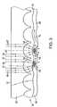
- FIG. 3shows an enlarged cross-sectional view of an optically active substrate.
- FIG. 4shows an embodiment of a chip cartridge used for examination of biological material.
- FIG. 1illustrates one embodiment of a confocal optical scanning and imaging system for examination of biological material located on, or near, an optically active substrate shown in FIG. 3 .
- the optically active substrateforms an important part of the optical system designed for increasing the signal-to-noise ratio of the detected optical signal.
- optical system 10includes a light source 12 , an entrance aperture 14 , a lens 16 , a dichroic mirror 20 , an objective lens 24 , a two or three axis translation table 28 , a lens 32 , an exit pinhole 34 , a band pass filter or a rejection filter 31 and a detector 36 .
- optical system 10is arranged for the detection of fluorescent light; however, optical system 10 may also be arranged for the detection of scattered or transmitted light at the irradiation wavelength.
- Light source 12emits an excitation light beam 15 , and dichroic mirror 20 directs the excitation light toward objective lens 24 .
- Objective lens 24focuses light onto a pixel (A) located on or near an optically active substrate 26 . Fluorescent light emitted from pixel A is collected by objective lens 24 and transmitted through dichroic mirror 20 , over a light path 30 , toward and trough band pass or rejection filter 31 and to light detector 36 .
- apertures (pinholes) 14 and 34 and lenses 16 and 32provides to detector 36 fluorescent light from a selected depth (in the Z direction) of pixel A. At pixel A, light emitted from other depths in the Z direction is substantially blocked and doesn't pass through pinhole 34 .
- This spatial filterimproves the signal-to-noise ratio, which is known in the art.
- Light source 12is constructed to emit light of a wavelength capable of exciting fluorophores associated with the examined biological tissue located on the optically active substrate.
- optically active substrate 50is transparent and includes optically active surface 52 with a dense array of micro-optical elements 54 .
- Micro-optical elements 54are arranged to support biological material 68 .
- Micro-optical elements 54may be formed by microlens cavities 56 or other optical elements located on surface 52 .
- light source 12emits simultaneously or sequentially 473, 488 or 490 nm (or 532 nm, 638 nm or 745 nm) light directed to optically active substrate 26 by dichroic mirror 20 .
- the excitation light of 488 nmirradiates a pixel on the surface of substrate 26 , and excites fluorophores that emit fluorescent light, for example, in the range 515 nm to 595 nm.
- the examined biological tissuecan be labeled using various types of fluorophores (and their corresponding absorption maxima) are Fluorescein (488 nm), Dichloro-fluorescein (525 nm), Hexachloro-fluorescein (529 nm), Tetramethylrhodamine (550 nm), Rhodamine X (575 nm), Cy3TM (550 nm), Cy5TM (650 nm), Cy7TM (750 nm), and IRD40 (785 nm).
- Detector 36uses a suitable band pass or rejection filters for detecting the fluorescent light emitted from pixel A.
- objective lens 24has a large numerical aperture (a numerical aperture of at least above 0.1).
- Optical system 10can collect optical data over an array of pixels by displacing optically active substrate 26 (or optically active substrate 50 ) in the X and Y directions using a translation table 28 .
- light source 12may be a lamp with a filter or a laser (solid state or gas laser such as an argon laser, a helium-neon laser, a diode laser, a dye laser, a titanium sapphire laser, a frequency-doubled diode pumped Nd:YAG laser, or a krypton laser).
- the excitation sourceilluminates the sample with an excitation wavelength that is within the visible spectrum, but other wavelengths (i.e., ultraviolet or near infrared wavelengths) may be used depending on the type of markers or samples or detection methods.
- Light detector 36may be a photomultiplier (PMT), a diode, a CCD array, or another photodetector.
- PMTphotomultiplier
- FIG. 1Ais a block diagram of an optical scanning system 40 , which includes at least one light source, several optical detectors, a light path system for providing optical coupling, a fast scanning system, and a system controller.
- the light path systemmay include dichroic beamsplitters, spectral filters, pinholes and several channels for detecting wavelength specific radiation.
- the optical scanning system 40also uses the novel optically active substrates described in detail in connection with FIG. 3 .
- the optically active surfacehas a dense array of micro-optical elements, each having a dimension comparable to (or larger than) the wavelength of the radiation emitted from the light source.
- the micro-optical elementsare constructed and arranged to generate increased intensity radiation or excite an evanescent radiation in their close proximity.
- the optically active surfacemay be combined with other techniques for examination of biological material, which techniques are mentioned and incorporated by reference above.
- optical scanning system 10 or 40is used to obtain images of oligonucleotide microarrays to which fluorescently labeled DNA or RNA is bound, images of polypeptides or other polymer arrays, electrophoresis gels, or other biological specimens.
- the optically active surfaceimproves the efficiency of the detection process.
- a controller 85controls the entire operation of optical scanning system 40 including a beam scanner 48 .
- Scanning system 40specifically includes a laser 12 for providing radiation of a selected wavelength to a stationary light path system 12 .
- the emitted beam 41is partially reflected and partially transmitted by a beamsplitter 42 .
- the reflected portion of beam 41impinges upon a photodetector 43 B (optional), which is typically a photodiode used for laser power monitoring.
- the transmitted portion of beam 41traveling over a light path 44 , is reflected by a dichroic beamsplitter 45 , transmitted through a lens 46 and an aperture (pinhole) 47 , expanded to the desired diameter, and delivered to a beam scanner 48 .
- the beam scanning systemincludes several optical elements arranged for scanning a sample that may be located on a linear translation stage.
- Beam scanning system 48delivers sequentially a focused light beam to a series of pixels, and conveys reflected or fluorescent light from each pixel back to the light path system.
- Beam scanning system 48has several high scan rate embodiments discussed in detail below.
- Beam scanning system 48also provides the “return” light path (shown in FIGS. 2 and 3 ) for light re-emitted from a sample, and focuses the re-emitted light onto confocal pinhole 47 .
- Light transmitted through aperture 47is collimated by lens 46 .
- lens 46For example, light re-emitted from the sample having wavelengths less that 515 nm is reflected by beamsplitter 45 and partially reflected by beamsplitter 42 to arrive at photodetector 43 A.
- pinhole 47may be located in a light path 101 to spatially filter only the fluorescent radiation).
- Light transmitted through beamsplitter 45travels over light path 101 to the four optical channels 90 , 100 , 110 and 120 depending on its wavelength.
- the number of optical channels used in scanning system 40is optional.
- light of a wavelength between 515 ⁇ m and 545 nm, reflected by a dichroic beamsplitter 102passes through a filter 104 onto a photodetector 106 .
- Light reflected by a dichroic beamsplitter 112having a wavelength between 545 nm and 570 nm passes through a filter 114 and onto a photodetector 116 .
- a photodetector 126detects light having wavelengths between 570 nm and 595 nm, which passes through a filter 124 .
- Each optical channel 90 , 100 , 110 and 120may include a confocal pinhole adjacent to a lens (not shown in FIG. 1 ). Confocal pinhole transmits florescence originating from the focal plane of system 10 .
- beam scanning system 48may include a flying objective design (an oscillatory movement design or a linear movement design), a scanning XY design, or preobjective scanning design. These designs are diagrammatically shown in FIG. 2 as a box 60 (e.g. comprising a flying objective, a scanning mirror etc.). Beam scanning system 48 provides an irradiation beam 49 directed toward an optically transparent substrate 50 mounted on a flow cell 70 .
- flow cell 70is located on an XYZ stage 80 controlled by a controller 85 (which can also control the entire scanning system 40 and several elements of a hybridization system).
- Flow cell 70includes a body having a cavity 71 , which is about 50 ⁇ m to 1500 ⁇ m deep, having the bottom and sides of cavity 71 preferably light absorbing.
- Flow cell 70includes an inlet port 73 and an outlet port 74 .
- FIG. 2Ais a cross-sectional view of flow cell 70 with substrate 50 mounted on flow cell 70 using adhesive bonds 72 or by any other design.
- Substrate 50has an optically inactive surface 51 and an optically active surface 52 .
- Reagents, such as labeled targetsare injected into the cavity 71 through inlet port 73 by a pump 75 ( FIG. 2 ) or by using a syringe, as described in U.S. Pat. No. 5,631,734, which is incorporated by reference.
- the reagentsbind with one or more complementary probes located on surface 52 (located inside cavity 71 in the embodiment of FIG. 2 ).
- Flow cell 70may also include a temperature controller connected to a re-circulating bath device 76 , as described in U.S. Pat. No. 5,631,734. Flow cell 70 may also include an agitation system and several valves, containers and cavities as described in U.S. Pat. Nos. 5,945,335 and 6,140,044, which are incorporated by reference.
- optically transparent substrate 50has optically active surface 52 with a dense array of micro-optical elements 54 .
- Micro-optical elements 54may be formed by microlens cavities 56 or any other optical elements that provide “increased intensity” radiation or “evanescent” radiation.
- micro-optical elements 54include microlens cavities 56 with a high index film (coating or layer) 58 deposited by sputtering or another vacuum deposition.
- Microlens cavities 56have a radius or a width (section or another relevant dimension) in the range of 100 nm to 1 ⁇ m; that is, a fraction or a small multiple of the wavelength of interest.
- the diameter and depth of the microlens cavitiesmay define the thickness of the high index layer 58 , which may even completely fill the cavities.
- High index layer 58is made of titanium dioxide with an index of refraction of 2.4, gallium phosphate with an index of refraction 3.4, or other medium with suitable index of refraction.
- High index layer 58is designed to have a thickness depending on its transmission coefficient so that a relatively low transmission coefficient will cause acceptable optical losses.
- micro-optical elements 54are formed by parallel or semi-parallel groves, parallel or semi-parallel half cylinders, or other micro-structures.
- Substrate 50is made of a PMMA, Plexiglas® or a similar plastic with an index of refraction about 1.57.
- the microlens cavitiescould be created in the substrate by forced embossing at a proper temperature, or by casting against a suitably formed negative master (as used when creating CD and DVD discs).
- substrate 50is be made by etching, which is preferably done for glass or quartz.
- Micro-optical elements 54may perform one or several functions. Micro-optical elements 54 may launch an evanescent surface wave 78 ( FIG. 3 ) within biological material 68 (e.g., a spot of dehydrated or hydrated biological material). Micro-optical elements 54 may also serve as high NA optical element capable of gathering light emitted when the excitation radiation of the surface wave excites a fluorophore 69 located within or at the biological material. The micro-optical elements exhibit an efficient light gathering effect since they behave as a lenslets (or other optical elements) with a very high numerical aperture.
- micro-optical elements 54 and the selection of the refraction index of substrate 50permit the fluorescent emission from a fluorophore 69 to egress from the exposed surface of the support with a comparatively low divergence and preferably in a collimated manner, as shown by lines 67 in FIG. 3 .
- the emitted fluorescent radiationis collected by micro-optical elements 54 and transmitted back through the substrate.
- a detectorreceives the transmitted fluorescent radiation via an objective lens (or optical system) located in a reflection geometry.
- the emitted fluorescent radiationis collected by a lens (or an optical system) located in a transmission geometry.
- the detectorreceives fluorescent (or non-fluorescent) radiation that doesn't travel back through the substrate.
- micro-optical elements 54do not “intensify” the fluorescent radiation, but this radiation is not attenuated by the optically active substrate.
- scanning system 48includes an oscillatory or rotary design for displacing an objective lens, for example, as described in PCT Application PCT/US99/06097 (published as WO 99/47964) or U.S. Provisional Application 60/286,578, both which are incorporated by reference.
- the rotary designcaries a relatively simple and light objective lens, which is oscillated over the substrate area.
- the objective lensdelivers an excitation light beam to an array of pixels of the scanned sample.
- the rotary designincludes a periscopic structure that optically couples the scanning objective lens to the irradiation and detection light paths shown in FIG. 1 .
- the rotary architectureoffers both high speed scanning and a constant optical path length.
- the arc scanned by the objective lenscovers the width of substrate 50 in polar coordinates.
- Substrate 50is mounted on a translation stage for linear displacement.
- the data, acquired in polar coordinates for each slide position,is instantly converted to Cartesian coordinates by the instrument's computer so the image is then directly correlated with the microarray on substrate 50 .
- the objective lens, carried on the rotary support structuremay be an aspheric, one-element lens.
- the field of viewis always on axis, which eliminates all the common sources of lateral or chromatic aberrations found in preobjective scanner microscopes.
- beam scanning system 48may include a rectilinear flying objective design, as described, in U.S. Pat. No. 5,459,325 to Hueton et al., which are incorporated by reference.
- the rectilinear flying objective designincludes a lens mounted on a linear arm driven by a voice coil to perform a fast scan over sample substrate 50 in a first dimension.
- Substrate 50is mounted on a translation stage that displaces sample in a second dimension, and may also move substrate 50 in a third dimension (i.e., z direction) for focusing.
- the rectilinear flying objective designuses a reliable, low-cost, low-inertia, stable high-speed linear scanning system, which directly acquires the data in the Cartesian coordinate system.
- the optical datamay be acquired in both directions of the lens scan, thus doubling the effective scanning speed.
- the scanning systemincludes an stable and rigid structure that enables high frequency scanning.
- beam scanning system 48may include a preobjective scanning design described in U.S. Pat. No. 5,981,956 to Stern or in U.S. Pat. No. 5,631,734 to Stern et al., both of which are incorporated by reference.
- the preobjective scanning designuses a scanning mirror that scans the excitation beam over a large field of view objective that includes several elements to provide, for example, a 10 mm field of view. This large field of view objective has a comparatively low NA of about 0.25.
- the examined substrateis translated linearly under the objective whiled the excitation beam is scanned over the objective by a scanning mirror.
- the optically active substratecan be translated sideways and scanned to capture a second swath.
- the two swathsare later stitched together by the instrument's computer.
- optical scanning system 10may be replaced by an imaging system that uses a CCD array as described, for example, in U.S. Pat. No. 5,578,832, which is incorporated by reference.
- Scanning and imaging systems 10 and 40achieve a uniform performance (i.e., consistent data) over the entire surface of substrate 50 .
- the intensity uniformityis about 95% and the spatial uniformity is about 98%.
- the systemscan over a selected scan area (typically over a scan area of 20 mm ⁇ 65 mm) and have a resolution of about 2.0 ⁇ m to 4.0 ⁇ m, wherein 10 ⁇ m is a sufficient resolution for a 10 ⁇ m spot size.
- an evanescent fieldarises at the boundary between a high refractive index medium and an adjacent lower index medium due to total internal reflection, as where the parent field in the higher index medium penetrates into the lower index medium (i.e., the refraction angle becomes imaginary).
- This evanescent fieldis a continuation of the internal standing wave that in turn is a result of constructive interference of incident and reflected illumination at the interface. (In the quantum mechanical view, this penetration of the total reflection barrier is called photon tunneling.)
- the resultant intensitycan be several times larger than the intensity of the incident radiation.
- Evanescent fieldalso arises when propagating illumination is diffracted by a grating having the grating period smaller than the wavelength, such that the diffracted orders are evanescent (i.e., the diffraction angle becomes imaginary). Again, the resultant intensity can be several times larger than the intensity of the incident radiation.
- evanescent fielddecays exponentially with distance from the surface of the medium interface.
- the exponent of the decaydepends on the ratio of denser to lower indices of refraction at the boundary surface.
- evanescent fielddecays over a distance of only less than a micron; thus this is “near-field.”
- Near fieldincludes both propagating and non-propagating radiation near, that is, within a wavelength of the interface surface.
- biological medium 68has to be located close to the surface with the high-refractive index boundary (interface of the dielectric material), or close to the diffraction grating.
- the index of refraction of available materialsimposes a practical limit of about 2.4 in the visible spectrum, and about 3.5 in the near infra-red spectrum. Conversion by diffraction is limited only by the diffraction grating spatial period.
- the present embodimentscan use a diffraction grating having the spatial period of less than 40 nanometers.
- optically active substrate 52includes an interference grating buried under a small layer of high index glass.
- This optically active substrate 52is a modification of microscope slides described in U.S. Pat. Nos. 5,822,472 and 5,959,292 (which are incorporated by reference), and are available from Zeptosens AG (Witterswill Switzerland).
- the gratingdiffracts the incident light and/or light that has not been absorbed by the examined biological material (which is a very large fraction) and induces, at a suitable angle, an evanescent wave, which then interacts with the biological material.
- the intensity of the excited evanescent wavecan be one order of magnitude greater than that of the original incident light beam. Since the grating reflects the beam at a different angle for each wavelength, each slide can operate beneficially at their designed wavelength.
- FIG. 4show an embodiment of a cartridge 150 for packaging and handling substrate 50 .
- Cartridge 150includes a top casing 152 , a middle casing 154 and a bottom casing 156 made of a plastic material and arranged to encase a hybridization cavity.
- Bottom casing 156includes two fluid channels arranged in communication with two annular regions located in middle casing 154 .
- Middle casing 14includes a septum (or the like) located at the annular regions and arranged to seals fluids within two channels located in top casing 154 and in communication with the hybridization cavity, as described in detail in U.S. Pat. No. 5,945,334, which is incorporated by reference.
- Chip package 150also includes alignment holes 158 and 160 and several support structures for mounting or positioning the chip package relative to a scanner.
- the probe arraysmay be fabricated according to various techniques disclosed in U.S. Pat. No. 5,143,854 to Pirrung et al., PCT Application WO 92/10092, or U.S. Pat. Nos. 5,384,261; 5,405,783; 5,412,087; 5,424,186; 5,445,934; or 5,744,308 all of which are incorporated by reference.
- micro-optical elements 54provide high energy gathering in the proximity of the biological material 68 located on the probe arrays.
- a probeis a surface-immobilized molecule that is recognized by particular target and is sometimes referred to as a ligand.
- probesthat can be investigated by this invention include, but are not restricted to, agonists and antagonists for cell membrane receptors, toxins and venoms, viral epitopes, hormones (e.g., opioid peptides, steroids, etc.), hormone receptors, peptides, enzymes, enzyme substrates, cofactors, drugs, lectins, sugars, oligonucleotides or nucleic acids, oligosaccharides, proteins, and monoclonal antibodies.
- hormonese.g., opioid peptides, steroids, etc.
- hormone receptorse.g., enzymes, enzyme substrates, cofactors, drugs, lectins, sugars, oligonucleotides or nucleic acids, oligosaccharides, proteins, and monoclonal antibodies.
- a targetis a molecule that has an affinity for a given probe and is sometimes referred to as a receptor.
- Targetsmay be naturally-occurring or manmade molecules. Also, they can be employed in their unaltered state or as aggregates with other species. Targets may be attached, covalently or noncovalently, to a binding member, either directly or via a specific binding substance.
- targetswhich can be employed by this invention include, but are not restricted to, antibodies, cell membrane receptors, monoclonal antibodies and antisera reactive with specific antigenic determinants (such as on viruses, cells or other materials), drugs, oligonucleotides or nucleic acids, peptides, cofactors, lectins, sugars, polysaccharides, cells, cellular membranes, and organelles.
- Targetsare sometimes referred to in the art as anti-probes or anti-ligands.
- a “probe target pair”is formed when two macromolecules have combined through molecular recognition to form a complex.
- Substrate 50is preferably optically transparent, but it does not need to be optically transparent, for example, if used having optically active surface 52 facing incoming radiation beam 46 .
- Substrate 50may be fabricated of a wide range of material, either biological, nonbiological, organic, inorganic, or a combination of any of these, existing as particles, strands, precipitates, gels, sheets, tubing, spheres, containers, capillaries, pads, slices, films, plates, slides, etc.
- the substratemay have any convenient shape, such as a disc, square, sphere, circle, etc.
- the substrateis preferably flat but may take on a variety of alternative surface configurations. For example, the substrate may contain raised or depressed regions on which a sample is located.
- the substrate and its surfacepreferably form a rigid support on which the sample can be formed.
- the substrate and its surfaceare also chosen to provide appropriate light-absorbing characteristics.
- the substratemay be a polymerized Langmuir Blodgett film, functionalized glass, Si, Ge, GaAs, GaP, SiO 2 , SiN 4 , modified silicon, or any one of a wide variety of gels or polymers such as (poly)tetrafluoroethylene, (poly)vinylidenedifluoride, polystyrene, polycarbonate, or combinations thereof.
- Other materials with which the substrate can be composed ofwill be readily apparent to those skilled in the art upon review of this disclosure.
Landscapes
- Physics & Mathematics (AREA)
- Health & Medical Sciences (AREA)
- General Physics & Mathematics (AREA)
- Chemical & Material Sciences (AREA)
- Immunology (AREA)
- Analytical Chemistry (AREA)
- Life Sciences & Earth Sciences (AREA)
- General Health & Medical Sciences (AREA)
- Biochemistry (AREA)
- Pathology (AREA)
- Nuclear Medicine, Radiotherapy & Molecular Imaging (AREA)
- Optics & Photonics (AREA)
- Chemical Kinetics & Catalysis (AREA)
- Investigating, Analyzing Materials By Fluorescence Or Luminescence (AREA)
Abstract
Description
Claims (46)
Priority Applications (1)
| Application Number | Priority Date | Filing Date | Title |
|---|---|---|---|
| US10/311,820US7158224B2 (en) | 2000-06-25 | 2001-06-25 | Optically active substrates |
Applications Claiming Priority (3)
| Application Number | Priority Date | Filing Date | Title |
|---|---|---|---|
| US21398700P | 2000-06-25 | 2000-06-25 | |
| PCT/US2001/020177WO2002001194A1 (en) | 2000-06-25 | 2001-06-25 | Optically active substrates |
| US10/311,820US7158224B2 (en) | 2000-06-25 | 2001-06-25 | Optically active substrates |
Publications (2)
| Publication Number | Publication Date |
|---|---|
| US20040125370A1 US20040125370A1 (en) | 2004-07-01 |
| US7158224B2true US7158224B2 (en) | 2007-01-02 |
Family
ID=22797321
Family Applications (1)
| Application Number | Title | Priority Date | Filing Date |
|---|---|---|---|
| US10/311,820Expired - LifetimeUS7158224B2 (en) | 2000-06-25 | 2001-06-25 | Optically active substrates |
Country Status (3)
| Country | Link |
|---|---|
| US (1) | US7158224B2 (en) |
| EP (1) | EP1311824A4 (en) |
| WO (1) | WO2002001194A1 (en) |
Cited By (18)
| Publication number | Priority date | Publication date | Assignee | Title |
|---|---|---|---|---|
| US20070262265A1 (en)* | 2006-05-10 | 2007-11-15 | Maccraith Brian | Polymer biochip for detecting fluorescence |
| US20100259254A1 (en)* | 2007-10-25 | 2010-10-14 | Koninklijke Philips Electronics N.V. | Sensor device for target particles in a sample |
| US8670123B2 (en) | 2009-06-24 | 2014-03-11 | Koninklijke Philips N.V. | Optical biosensor with focusing optics |
| US20170067833A1 (en)* | 2015-09-09 | 2017-03-09 | Samsung Electronics Co., Ltd. | Substrate inspection apparatus |
| US9606058B2 (en) | 2014-08-08 | 2017-03-28 | Quantum-Si Incorporated | Integrated device for temporal binning of received photons |
| US9678012B2 (en) | 2014-08-08 | 2017-06-13 | Quantum-Si Incorporated | Integrated device with external light source for probing detecting and analyzing molecules |
| US9863880B2 (en) | 2013-11-17 | 2018-01-09 | Quantum-Si Incorporated | Optical system and assay chip for probing, detecting and analyzing molecules |
| US9921157B2 (en) | 2014-08-08 | 2018-03-20 | Quantum-Si Incorporated | Optical system and assay chip for probing, detecting and analyzing molecules |
| US10174363B2 (en) | 2015-05-20 | 2019-01-08 | Quantum-Si Incorporated | Methods for nucleic acid sequencing |
| US10845308B2 (en) | 2016-12-22 | 2020-11-24 | Quantum-Si Incorporated | Integrated photodetector with direct binning pixel |
| US10884227B2 (en) | 2016-11-10 | 2021-01-05 | The Trustees Of Columbia University In The City Of New York | Rapid high-resolution imaging methods for large samples |
| US11344200B2 (en) | 2016-02-17 | 2022-05-31 | Tesseract Health, Inc. | Sensor and device for lifetime imaging and detection applications |
| US11391626B2 (en) | 2018-06-22 | 2022-07-19 | Quantum-Si Incorporated | Integrated photodetector with charge storage bin of varied detection time |
| US11505796B2 (en) | 2021-03-11 | 2022-11-22 | Nautilus Biotechnology, Inc. | Systems and methods for biomolecule retention |
| US11970693B2 (en) | 2017-08-18 | 2024-04-30 | Nautilus Subsidiary, Inc. | Methods of selecting binding reagents |
| US11993865B2 (en) | 2018-11-20 | 2024-05-28 | Nautilus Subsidiary, Inc. | Selection of affinity reagents |
| US12078596B2 (en) | 2017-07-24 | 2024-09-03 | Quantum-Si Incorporated | Hand-held, massively-parallel, bio-optoelectronic instrument |
| US12306093B2 (en) | 2019-04-29 | 2025-05-20 | Nautilus Subsidiary, Inc. | Methods and systems for integrated on-chip single-molecule detection |
Families Citing this family (43)
| Publication number | Priority date | Publication date | Assignee | Title |
|---|---|---|---|---|
| US7277166B2 (en)* | 2000-08-02 | 2007-10-02 | Honeywell International Inc. | Cytometer analysis cartridge optical configuration |
| US6804679B2 (en) | 2001-03-12 | 2004-10-12 | Affymetrix, Inc. | System, method, and user interfaces for managing genomic data |
| US7901630B2 (en) | 2002-08-20 | 2011-03-08 | Illumina, Inc. | Diffraction grating-based encoded microparticle assay stick |
| US7923260B2 (en) | 2002-08-20 | 2011-04-12 | Illumina, Inc. | Method of reading encoded particles |
| US7872804B2 (en) | 2002-08-20 | 2011-01-18 | Illumina, Inc. | Encoded particle having a grating with variations in the refractive index |
| US7164533B2 (en) | 2003-01-22 | 2007-01-16 | Cyvera Corporation | Hybrid random bead/chip based microarray |
| US7508608B2 (en) | 2004-11-17 | 2009-03-24 | Illumina, Inc. | Lithographically fabricated holographic optical identification element |
| US7619819B2 (en) | 2002-08-20 | 2009-11-17 | Illumina, Inc. | Method and apparatus for drug product tracking using encoded optical identification elements |
| US7900836B2 (en) | 2002-08-20 | 2011-03-08 | Illumina, Inc. | Optical reader system for substrates having an optically readable code |
| US7441703B2 (en) | 2002-08-20 | 2008-10-28 | Illumina, Inc. | Optical reader for diffraction grating-based encoded optical identification elements |
| US7349158B2 (en) | 2002-09-12 | 2008-03-25 | Cyvera Corporation | Diffraction grating-based encoded micro-particles for multiplexed experiments |
| US7092160B2 (en) | 2002-09-12 | 2006-08-15 | Illumina, Inc. | Method of manufacturing of diffraction grating-based optical identification element |
| US20100255603A9 (en)* | 2002-09-12 | 2010-10-07 | Putnam Martin A | Method and apparatus for aligning microbeads in order to interrogate the same |
| AU2003267192A1 (en) | 2002-09-12 | 2004-04-30 | Cyvera Corporation | Method and apparatus for aligning elongated microbeads in order to interrogate the same |
| US7433123B2 (en)* | 2004-02-19 | 2008-10-07 | Illumina, Inc. | Optical identification element having non-waveguide photosensitive substrate with diffraction grating therein |
| US20060088844A1 (en)* | 2004-10-22 | 2006-04-27 | Honeywell International Inc. | Real-time PCR microarray based on evanescent wave biosensor |
| WO2006055735A2 (en)* | 2004-11-16 | 2006-05-26 | Illumina, Inc | Scanner having spatial light modulator |
| ATE459933T1 (en) | 2004-11-16 | 2010-03-15 | Illumina Inc | METHOD AND APPARATUS FOR READING CODED MICROBALLS |
| US7604173B2 (en) | 2004-11-16 | 2009-10-20 | Illumina, Inc. | Holographically encoded elements for microarray and other tagging labeling applications, and method and apparatus for making and reading the same |
| CA2540474A1 (en)* | 2005-04-01 | 2006-10-01 | Uti Limited Partnership | Cytometer |
| EP1910809A1 (en)* | 2005-07-21 | 2008-04-16 | Koninklijke Philips Electronics N.V. | Device for detection of excitation using a multiple spot arrangement |
| CN101278186A (en)* | 2005-10-03 | 2008-10-01 | 皇家飞利浦电子股份有限公司 | Biosensors with improved sensitivity |
| US7623624B2 (en) | 2005-11-22 | 2009-11-24 | Illumina, Inc. | Method and apparatus for labeling using optical identification elements characterized by X-ray diffraction |
| CN101331390A (en)* | 2005-12-15 | 2008-12-24 | 皇家飞利浦电子股份有限公司 | Device for analyzing a sample |
| US7286232B2 (en)* | 2006-02-15 | 2007-10-23 | Li-Cor, Inc. | Fluorescence filtering system and method for molecular imaging |
| US7830575B2 (en) | 2006-04-10 | 2010-11-09 | Illumina, Inc. | Optical scanner with improved scan time |
| WO2008092291A1 (en)* | 2007-01-17 | 2008-08-07 | Honeywell International Inc. | Microarray reader based on evanescent wave detection and method of reading a microarray |
| FR2930031A1 (en)* | 2008-04-14 | 2009-10-16 | Centre Nat Rech Scient | DEVICE AND METHOD FOR EXAMINED ANALYSIS OF A PARTICLE SAMPLE. |
| US8809810B2 (en) | 2010-05-20 | 2014-08-19 | Honeywell International Inc. | Microarray reader based on evanescent wave detection |
| TW201202683A (en)* | 2010-07-09 | 2012-01-16 | Yayatech Co Ltd | High performance light source for photofluorography |
| JP5221614B2 (en)* | 2010-09-17 | 2013-06-26 | 独立行政法人科学技術振興機構 | Three-dimensional confocal observation device and observation focal plane displacement / correction unit |
| WO2014021808A1 (en)* | 2012-07-29 | 2014-02-06 | Hewlett-Packard Development Company, L.P. | Scattering spectroscopy nanosensor |
| US20140333998A1 (en)* | 2013-03-12 | 2014-11-13 | Board Of Trustees, Southern Illinois University | Micro-lens for high resolution microscopy |
| EP3066190B1 (en) | 2013-11-06 | 2020-12-30 | Becton, Dickinson and Company | Microfluidic devices, and methods of using the same |
| EP3074754B1 (en)* | 2013-11-13 | 2025-03-05 | Becton, Dickinson and Company | Microimager analysis system comprising optics and methods of use thereof |
| AU2015228548B2 (en) | 2014-03-10 | 2019-11-21 | Amo Groningen B.V. | Piggyback intraocular lens that improves overall vision where there is a local loss of retinal function |
| EP3278166A2 (en) | 2015-03-31 | 2018-02-07 | Samantree Medical SA | Systems and methods for in-operating-theatre imaging of fresh tissue resected during surgery for pathology assessment |
| US10908072B2 (en) | 2016-12-15 | 2021-02-02 | The Board Of Regents Of The University Of Texas System | Total internal reflection and transmission illumination fluorescence microscopy imaging system with improved background suppression |
| JP6439810B2 (en)* | 2017-02-06 | 2018-12-19 | 横河電機株式会社 | Biochip, biochip unit, biochip reader, and biochip manufacturing method |
| US10928621B2 (en) | 2017-10-31 | 2021-02-23 | Samantree Medical Sa | Sample dishes for use in microscopy and methods of their use |
| US11747603B2 (en) | 2017-10-31 | 2023-09-05 | Samantree Medical Sa | Imaging systems with micro optical element arrays and methods of specimen imaging |
| US10539776B2 (en)* | 2017-10-31 | 2020-01-21 | Samantree Medical Sa | Imaging systems with micro optical element arrays and methods of specimen imaging |
| US10816473B2 (en)* | 2018-01-22 | 2020-10-27 | Verily Life Sciences Llc | High-throughput hyperspectral imaging systems |
Citations (92)
| Publication number | Priority date | Publication date | Assignee | Title |
|---|---|---|---|---|
| US4400056A (en) | 1980-07-09 | 1983-08-23 | Her Majesty The Queen As Represented By The Minister Of National Defence Of Her Majesty's Canadian Government | Evanescent-wave fiber reflector |
| US4604520A (en) | 1982-12-27 | 1986-08-05 | International Business Machines Corporation | Optical near-field scanning microscope |
| US4649280A (en) | 1985-05-10 | 1987-03-10 | The University Of Rochester | Method and system for the enhancement of fluorescence |
| US4681451A (en) | 1986-02-28 | 1987-07-21 | Polaroid Corporation | Optical proximity imaging method and apparatus |
| US4815843A (en) | 1985-05-29 | 1989-03-28 | Oerlikon-Buhrle Holding Ag | Optical sensor for selective detection of substances and/or for the detection of refractive index changes in gaseous, liquid, solid and porous samples |
| US4917462A (en) | 1988-06-15 | 1990-04-17 | Cornell Research Foundation, Inc. | Near field scanning optical microscopy |
| US5004307A (en) | 1990-04-12 | 1991-04-02 | The Board Of Trustees Of The Leland Stanford Junior University | Near field and solid immersion optical microscope |
| US5018865A (en) | 1988-10-21 | 1991-05-28 | Ferrell Thomas L | Photon scanning tunneling microscopy |
| US5028802A (en) | 1990-01-11 | 1991-07-02 | Eye Research Institute Of Retina Foundation | Imaging apparatus and methods utilizing scannable microlaser source |
| US5081012A (en) | 1988-03-29 | 1992-01-14 | Applied Research Systems Ars Holding N.V. | Waveguide sensor with input and reflecting gratings and its use in immunoassay |
| US5082629A (en) | 1989-12-29 | 1992-01-21 | The Board Of The University Of Washington | Thin-film spectroscopic sensor |
| US5120131A (en) | 1988-02-14 | 1992-06-09 | Walter Lukosz | Method and apparatus for selecting detection of changes in samples by integrated optical interference |
| US5125750A (en) | 1991-03-14 | 1992-06-30 | The Board Of Trustees Of The Leland Stanford Junior University | Optical recording system employing a solid immersion lens |
| WO1992015862A1 (en) | 1991-03-11 | 1992-09-17 | John Mcgilp | A waveguide sensor |
| US5166515A (en) | 1989-06-22 | 1992-11-24 | Applied Research Systems Ars Holding, N.V. | Method of optical analysis of a fluid including an optical waveguide |
| US5272330A (en) | 1990-11-19 | 1993-12-21 | At&T Bell Laboratories | Near field scanning optical microscope having a tapered waveguide |
| US5304795A (en) | 1991-10-03 | 1994-04-19 | Seiko Instruments Inc. | High resolution observation apparatus with photon scanning microscope |
| US5341215A (en) | 1991-06-08 | 1994-08-23 | Hewlett-Packard Company | Method and apparatus for detecting the presence and/or concentration of biomolecules |
| US5351318A (en) | 1993-04-05 | 1994-09-27 | The Board Of Trustees Of The Leland Stanford Jr./University | Fiber optic communication system and fiber optic modulator |
| US5351127A (en) | 1992-06-17 | 1994-09-27 | Hewlett-Packard Company | Surface plasmon resonance measuring instruments |
| US5352582A (en) | 1993-10-28 | 1994-10-04 | Hewlett-Packard Company | Holographic based bio-assay |
| US5369717A (en) | 1990-04-11 | 1994-11-29 | Applied Research System Ars Holding N.V. | Optical waveguide assay unit and method of improving assay sensitivity using same |
| US5410151A (en) | 1993-07-15 | 1995-04-25 | Sumitomo Electric Lightwave Corp. | Fiber optic probe and method of making same |
| US5424841A (en) | 1993-05-28 | 1995-06-13 | Molecular Dynamics | Apparatus for measuring spatial distribution of fluorescence on a substrate |
| US5437840A (en) | 1994-04-15 | 1995-08-01 | Hewlett-Packard Company | Apparatus for intracavity sensing of macroscopic properties of chemicals |
| US5442169A (en) | 1991-04-26 | 1995-08-15 | Paul Scherrer Institut | Method and apparatus for determining a measuring variable by means of an integrated optical sensor module |
| US5452382A (en) | 1992-09-07 | 1995-09-19 | Nikon Corporation | Optical waveguide device and optical microscope using the same |
| WO1995033197A1 (en) | 1994-05-27 | 1995-12-07 | Ciba-Geigy Ag | Process for detecting evanescently excited luminescence |
| US5478755A (en) | 1988-07-25 | 1995-12-26 | Ares Serono Research & Development Ltd. | Long range surface plasma resonance immunoassay |
| US5485536A (en) | 1994-10-13 | 1996-01-16 | Accuphotonics, Inc. | Fiber optic probe for near field optical microscopy |
| US5497359A (en) | 1994-08-30 | 1996-03-05 | National Business Machines Corporation | Optical disk data storage system with radiation-transparent air-bearing slider |
| WO1996018205A1 (en) | 1994-12-08 | 1996-06-13 | Molecular Dynamics, Inc. | Fluorescence imaging system employing a macro scanning objective |
| US5548113A (en) | 1994-03-24 | 1996-08-20 | Trustees Of Boston University | Co-axial detection and illumination with shear force dithering in a near-field scanning optical microscope |
| WO1996036062A1 (en) | 1995-05-10 | 1996-11-14 | Molecular Dynamics, Inc. | Led point scanning system |
| US5577137A (en) | 1995-02-22 | 1996-11-19 | American Research Corporation Of Virginia | Optical chemical sensor and method using same employing a multiplicity of fluorophores contained in the free volume of a polymeric optical waveguide or in pores of a ceramic waveguide |
| US5585639A (en) | 1995-07-27 | 1996-12-17 | Hewlett-Packard Company | Optical scanning apparatus |
| US5631170A (en) | 1992-06-10 | 1997-05-20 | Applied Research Systems Ars Holding N.V. | Method for improving measurement precision in evanescent wave optical biosensor assays |
| US5633724A (en) | 1995-08-29 | 1997-05-27 | Hewlett-Packard Company | Evanescent scanning of biochemical array |
| WO1997028439A1 (en) | 1996-02-01 | 1997-08-07 | Molecular Dynamics, Inc. | Fluorescence imaging system compatible with macro and micro scanning objectives |
| US5664036A (en) | 1994-10-13 | 1997-09-02 | Accuphotonics, Inc. | High resolution fiber optic probe for near field optical microscopy and method of making same |
| US5675145A (en) | 1994-07-06 | 1997-10-07 | Olympus Optical Co., Ltd. | Scanning probe microscope having an optical system for enabling identification of the scanning region and sample observation during a scanning operation |
| US5689480A (en) | 1996-08-13 | 1997-11-18 | The Board Of Trustees Of The Leland Stanford Junior University | Magneto-optic recording system employing near field optics |
| US5712705A (en) | 1993-11-15 | 1998-01-27 | Carl Zeiss Jena Gmbh | Arrangement for analysis of substances at the surface of an optical sensor |
| US5736410A (en) | 1992-09-14 | 1998-04-07 | Sri International | Up-converting reporters for biological and other assays using laser excitation techniques |
| US5738825A (en) | 1993-07-20 | 1998-04-14 | Balzers Aktiengesellschaft | Optical biosensor matrix |
| US5754514A (en) | 1996-10-08 | 1998-05-19 | Polaroid Corporation | Phase controlled evanescent field systems and methods for optical recording and retrieval |
| WO1998022799A2 (en) | 1996-11-18 | 1998-05-28 | Novartis Ag | Measurement device and its use |
| US5763870A (en) | 1996-12-13 | 1998-06-09 | Hewlett-Packard Company | Method and system for operating a laser device employing an integral power-regulation sensor |
| US5764840A (en) | 1995-11-20 | 1998-06-09 | Visionex, Inc. | Optical fiber with enhanced light collection and illumination and having highly controlled emission and acceptance patterns |
| US5796487A (en) | 1996-06-28 | 1998-08-18 | Polaroid Corporation | Dark field, photon tunneling imaging systems and methods for optical recording and retrieval |
| US5796909A (en) | 1996-02-14 | 1998-08-18 | Islam; Mohammed N. | All-fiber, high-sensitivity, near-field optical microscopy instrument employing guided wave light collector and specimen support |
| US5800992A (en) | 1989-06-07 | 1998-09-01 | Fodor; Stephen P.A. | Method of detecting nucleic acids |
| US5808790A (en) | 1996-01-25 | 1998-09-15 | Nikon Corporation | Integrated microscope providing near-field and light microscopy |
| US5812272A (en) | 1997-01-30 | 1998-09-22 | Hewlett-Packard Company | Apparatus and method with tiled light source array for integrated assay sensing |
| US5812723A (en) | 1994-03-24 | 1998-09-22 | Kanagawa Academy Of Science And Technology | Optical fiber with tapered end of core protruding from clad |
| US5821410A (en) | 1996-09-20 | 1998-10-13 | Regents Of The University Of California | Scanning tip microwave near field microscope |
| US5827748A (en) | 1997-01-24 | 1998-10-27 | The United States Of America As Represented By The Secretary Of The Navy | Chemical sensor using two-dimensional lens array |
| US5837475A (en) | 1997-01-30 | 1998-11-17 | Hewlett-Packard Co. | Apparatus and method for scanning a chemical array |
| WO1998052481A1 (en)* | 1997-05-23 | 1998-11-26 | Medical Laser Technologies Limited | Apparatus and method for delivery of light to skin |
| US5859814A (en) | 1996-10-18 | 1999-01-12 | The Board Of Trustees Of The Leland Stanford Junior University | Magneto-optic recording system and method |
| US5871628A (en)* | 1996-08-22 | 1999-02-16 | The University Of Texas System | Automatic sequencer/genotyper having extended spectral response |
| US5883872A (en) | 1997-05-29 | 1999-03-16 | The Board Of Trustees Of The Leland Stanford Junior University | Near field magneto-optical recording system employing slit illumination |
| WO1999013320A1 (en) | 1997-09-10 | 1999-03-18 | Artificial Sensing Instruments Asi Ag | Optical sensor and optical method for characterizing a chemical or biological substance |
| US5892857A (en) | 1997-01-21 | 1999-04-06 | Molecular Optoelectronics Corporation | Electro-optic compound waveguide intensity modular and method using same |
| US5900949A (en) | 1996-05-23 | 1999-05-04 | Hewlett-Packard Company | CCD imager for confocal scanning microscopy |
| US5907425A (en) | 1995-12-19 | 1999-05-25 | The Board Of Trustees Of The Leland Stanford Junior University | Miniature scanning confocal microscope |
| US5910940A (en) | 1996-10-08 | 1999-06-08 | Polaroid Corporation | Storage medium having a layer of micro-optical lenses each lens generating an evanescent field |
| US5939709A (en) | 1997-06-19 | 1999-08-17 | Ghislain; Lucien P. | Scanning probe optical microscope using a solid immersion lens |
| US5953477A (en) | 1995-11-20 | 1999-09-14 | Visionex, Inc. | Method and apparatus for improved fiber optic light management |
| WO1999047705A1 (en) | 1998-03-19 | 1999-09-23 | Novartis Ag | Detection method |
| US5969345A (en) | 1997-04-30 | 1999-10-19 | University Of Utah Research Foundation | Micromachined probes for nanometer scale measurements and methods of making such probes |
| US5971193A (en) | 1997-06-13 | 1999-10-26 | Veetop Corporation | Container for swimming pool maintenance accessories and related methods |
| US5980831A (en) | 1996-06-17 | 1999-11-09 | Braiman; Mark S. | Support planar germanium waveguides for infrared evanescent-wave sensing |
| WO1999063326A1 (en) | 1998-05-29 | 1999-12-09 | Photonic Research Systems Limited | Evanescent-wave excitation of upconverting labels |
| US6002704A (en) | 1997-01-25 | 1999-12-14 | Innolight Innovative Laser Und Systemtechnik Gmbh | Monolithic, non-planar ring laser with Q-switched single-frequency operation |
| US6006119A (en)* | 1998-02-04 | 1999-12-21 | Polestar Technologies, Inc. | Non-invasive optical measurement of blood hematocrit |
| US6016376A (en) | 1997-10-06 | 2000-01-18 | Nec Research Institute, Inc. | Tapered coherent fiber bundle imaging device for near-field optical microscopy |
| US6026205A (en) | 1997-01-21 | 2000-02-15 | Molecular Optoelectronics Corporation | Compound optical waveguide and filter applications thereof |
| WO2000020848A1 (en) | 1998-10-02 | 2000-04-13 | Marconi Electronic Systems Limited | Integrated optical waveguide chemical sensor with bragg grating |
| US6064785A (en) | 1997-09-30 | 2000-05-16 | Pioneer Electronic Corporation | Optical wave guide path recording medium and optical reproducing apparatus |
| US6078705A (en) | 1995-05-12 | 2000-06-20 | Novartis Ag | Sensor platform and method for the parallel detection of a plurality of analytes using evanescently excited luminescence |
| WO2000062105A1 (en) | 1999-04-09 | 2000-10-19 | The Government Of The United States Of America As Represented By The Secretary Of The Navy | Reflectively coated optical waveguide and fluidics cell integration |
| US6140044A (en) | 1994-06-08 | 2000-10-31 | Affymetrix, Inc. | Method and apparatus for packaging a probe array |
| US6177990B1 (en) | 1997-05-23 | 2001-01-23 | Molecular Dynamics, Inc. | Optical substrate for enhanced detectability of fluorescence |
| US6201639B1 (en) | 1998-03-20 | 2001-03-13 | James W. Overbeck | Wide field of view and high speed scanning microscopy |
| WO2001018524A2 (en) | 1999-08-30 | 2001-03-15 | Illumina, Inc. | Methods for improving signal detection from an array |
| US6294327B1 (en) | 1997-09-08 | 2001-09-25 | Affymetrix, Inc. | Apparatus and method for detecting samples labeled with material having strong light scattering properties, using reflection mode light and diffuse scattering |
| WO2001079821A1 (en) | 2000-04-14 | 2001-10-25 | Zeptosens Ag | Grid-waveguide structure for reinforcing an excitation field and use thereof |
| US6393035B1 (en) | 1999-02-01 | 2002-05-21 | Gigatera Ag | High-repetition rate passively mode-locked solid-state laser |
| US6395558B1 (en) | 1996-08-29 | 2002-05-28 | Zeptosens Ag | Optical chemical/biochemical sensor |
| US6437345B1 (en) | 1998-05-14 | 2002-08-20 | Zeptosens Ag | Sensing unit provided with separated detection light guiding |
| US20020132261A1 (en) | 2000-01-28 | 2002-09-19 | Dorsel Andreas N. | Multi-featured arrays with reflective coating |
Family Cites Families (9)
| Publication number | Priority date | Publication date | Assignee | Title |
|---|---|---|---|---|
| US5266515A (en)* | 1992-03-02 | 1993-11-30 | Motorola, Inc. | Fabricating dual gate thin film transistors |
| US5674698A (en)* | 1992-09-14 | 1997-10-07 | Sri International | Up-converting reporters for biological and other assays using laser excitation techniques |
| US5631734A (en)* | 1994-02-10 | 1997-05-20 | Affymetrix, Inc. | Method and apparatus for detection of fluorescently labeled materials |
| US5981956A (en)* | 1996-05-16 | 1999-11-09 | Affymetrix, Inc. | Systems and methods for detection of labeled materials |
| DE19725050C2 (en)* | 1997-06-13 | 1999-06-24 | Fraunhofer Ges Forschung | Arrangement for the detection of biochemical or chemical substances by means of fluorescent light excitation and method for their production |
| DE19748211A1 (en)* | 1997-10-31 | 1999-05-06 | Zeiss Carl Fa | Optical array system and reader for microtiter plates |
| US6100541A (en)* | 1998-02-24 | 2000-08-08 | Caliper Technologies Corporation | Microfluidic devices and systems incorporating integrated optical elements |
| US5973839A (en)* | 1998-03-05 | 1999-10-26 | Hewlett-Packard Company | Optical homogenizer |
| DE19846928A1 (en)* | 1998-10-12 | 2000-04-13 | Zeiss Carl Fa | Imaging system, especially in a high throughput automatic analyzer useful for drug development or medical diagnosis, has a cylindrical lens array combined with or preceded by a prism array |
- 2001
- 2001-06-25EPEP01948692Apatent/EP1311824A4/ennot_activeWithdrawn
- 2001-06-25WOPCT/US2001/020177patent/WO2002001194A1/enactiveApplication Filing
- 2001-06-25USUS10/311,820patent/US7158224B2/ennot_activeExpired - Lifetime
Patent Citations (99)
| Publication number | Priority date | Publication date | Assignee | Title |
|---|---|---|---|---|
| US4400056A (en) | 1980-07-09 | 1983-08-23 | Her Majesty The Queen As Represented By The Minister Of National Defence Of Her Majesty's Canadian Government | Evanescent-wave fiber reflector |
| US4604520A (en) | 1982-12-27 | 1986-08-05 | International Business Machines Corporation | Optical near-field scanning microscope |
| US4649280A (en) | 1985-05-10 | 1987-03-10 | The University Of Rochester | Method and system for the enhancement of fluorescence |
| US4815843A (en) | 1985-05-29 | 1989-03-28 | Oerlikon-Buhrle Holding Ag | Optical sensor for selective detection of substances and/or for the detection of refractive index changes in gaseous, liquid, solid and porous samples |
| US4681451A (en) | 1986-02-28 | 1987-07-21 | Polaroid Corporation | Optical proximity imaging method and apparatus |
| US5120131A (en) | 1988-02-14 | 1992-06-09 | Walter Lukosz | Method and apparatus for selecting detection of changes in samples by integrated optical interference |
| US5081012A (en) | 1988-03-29 | 1992-01-14 | Applied Research Systems Ars Holding N.V. | Waveguide sensor with input and reflecting gratings and its use in immunoassay |
| US4917462A (en) | 1988-06-15 | 1990-04-17 | Cornell Research Foundation, Inc. | Near field scanning optical microscopy |
| US5478755A (en) | 1988-07-25 | 1995-12-26 | Ares Serono Research & Development Ltd. | Long range surface plasma resonance immunoassay |
| US5018865A (en) | 1988-10-21 | 1991-05-28 | Ferrell Thomas L | Photon scanning tunneling microscopy |
| US5800992A (en) | 1989-06-07 | 1998-09-01 | Fodor; Stephen P.A. | Method of detecting nucleic acids |
| US5166515A (en) | 1989-06-22 | 1992-11-24 | Applied Research Systems Ars Holding, N.V. | Method of optical analysis of a fluid including an optical waveguide |
| US5082629A (en) | 1989-12-29 | 1992-01-21 | The Board Of The University Of Washington | Thin-film spectroscopic sensor |
| US5028802A (en) | 1990-01-11 | 1991-07-02 | Eye Research Institute Of Retina Foundation | Imaging apparatus and methods utilizing scannable microlaser source |
| US5369717A (en) | 1990-04-11 | 1994-11-29 | Applied Research System Ars Holding N.V. | Optical waveguide assay unit and method of improving assay sensitivity using same |
| US5004307A (en) | 1990-04-12 | 1991-04-02 | The Board Of Trustees Of The Leland Stanford Junior University | Near field and solid immersion optical microscope |
| US5272330A (en) | 1990-11-19 | 1993-12-21 | At&T Bell Laboratories | Near field scanning optical microscope having a tapered waveguide |
| WO1992015862A1 (en) | 1991-03-11 | 1992-09-17 | John Mcgilp | A waveguide sensor |
| US5125750A (en) | 1991-03-14 | 1992-06-30 | The Board Of Trustees Of The Leland Stanford Junior University | Optical recording system employing a solid immersion lens |
| US5442169A (en) | 1991-04-26 | 1995-08-15 | Paul Scherrer Institut | Method and apparatus for determining a measuring variable by means of an integrated optical sensor module |
| US5341215A (en) | 1991-06-08 | 1994-08-23 | Hewlett-Packard Company | Method and apparatus for detecting the presence and/or concentration of biomolecules |
| US5304795A (en) | 1991-10-03 | 1994-04-19 | Seiko Instruments Inc. | High resolution observation apparatus with photon scanning microscope |
| US5631170A (en) | 1992-06-10 | 1997-05-20 | Applied Research Systems Ars Holding N.V. | Method for improving measurement precision in evanescent wave optical biosensor assays |
| US5351127A (en) | 1992-06-17 | 1994-09-27 | Hewlett-Packard Company | Surface plasmon resonance measuring instruments |
| US5452382A (en) | 1992-09-07 | 1995-09-19 | Nikon Corporation | Optical waveguide device and optical microscope using the same |
| US5736410A (en) | 1992-09-14 | 1998-04-07 | Sri International | Up-converting reporters for biological and other assays using laser excitation techniques |
| US5351318A (en) | 1993-04-05 | 1994-09-27 | The Board Of Trustees Of The Leland Stanford Jr./University | Fiber optic communication system and fiber optic modulator |
| US5424841A (en) | 1993-05-28 | 1995-06-13 | Molecular Dynamics | Apparatus for measuring spatial distribution of fluorescence on a substrate |
| US5410151A (en) | 1993-07-15 | 1995-04-25 | Sumitomo Electric Lightwave Corp. | Fiber optic probe and method of making same |
| US5738825A (en) | 1993-07-20 | 1998-04-14 | Balzers Aktiengesellschaft | Optical biosensor matrix |
| US5352582A (en) | 1993-10-28 | 1994-10-04 | Hewlett-Packard Company | Holographic based bio-assay |
| US5712705A (en) | 1993-11-15 | 1998-01-27 | Carl Zeiss Jena Gmbh | Arrangement for analysis of substances at the surface of an optical sensor |
| US5812723A (en) | 1994-03-24 | 1998-09-22 | Kanagawa Academy Of Science And Technology | Optical fiber with tapered end of core protruding from clad |
| US5548113A (en) | 1994-03-24 | 1996-08-20 | Trustees Of Boston University | Co-axial detection and illumination with shear force dithering in a near-field scanning optical microscope |
| US5928525A (en) | 1994-03-24 | 1999-07-27 | Kanagawa Academy Of Science And Technology | Method for optical fiber with tapered end core protruding from clad |
| US5437840A (en) | 1994-04-15 | 1995-08-01 | Hewlett-Packard Company | Apparatus for intracavity sensing of macroscopic properties of chemicals |
| WO1995033197A1 (en) | 1994-05-27 | 1995-12-07 | Ciba-Geigy Ag | Process for detecting evanescently excited luminescence |
| US5822472A (en) | 1994-05-27 | 1998-10-13 | Novartis Corporation | Process for detecting evanescently excited luminescence |
| US5959292A (en) | 1994-05-27 | 1999-09-28 | Novartis Corporation | Process for detecting evanescently excited luminescence |
| US6140044A (en) | 1994-06-08 | 2000-10-31 | Affymetrix, Inc. | Method and apparatus for packaging a probe array |
| US5675145A (en) | 1994-07-06 | 1997-10-07 | Olympus Optical Co., Ltd. | Scanning probe microscope having an optical system for enabling identification of the scanning region and sample observation during a scanning operation |
| US5497359A (en) | 1994-08-30 | 1996-03-05 | National Business Machines Corporation | Optical disk data storage system with radiation-transparent air-bearing slider |
| US5485536A (en) | 1994-10-13 | 1996-01-16 | Accuphotonics, Inc. | Fiber optic probe for near field optical microscopy |
| US5664036A (en) | 1994-10-13 | 1997-09-02 | Accuphotonics, Inc. | High resolution fiber optic probe for near field optical microscopy and method of making same |
| WO1996018205A1 (en) | 1994-12-08 | 1996-06-13 | Molecular Dynamics, Inc. | Fluorescence imaging system employing a macro scanning objective |
| US5577137A (en) | 1995-02-22 | 1996-11-19 | American Research Corporation Of Virginia | Optical chemical sensor and method using same employing a multiplicity of fluorophores contained in the free volume of a polymeric optical waveguide or in pores of a ceramic waveguide |
| WO1996036062A1 (en) | 1995-05-10 | 1996-11-14 | Molecular Dynamics, Inc. | Led point scanning system |
| US5578818A (en) | 1995-05-10 | 1996-11-26 | Molecular Dynamics | LED point scanning system |
| US6078705A (en) | 1995-05-12 | 2000-06-20 | Novartis Ag | Sensor platform and method for the parallel detection of a plurality of analytes using evanescently excited luminescence |
| US5585639A (en) | 1995-07-27 | 1996-12-17 | Hewlett-Packard Company | Optical scanning apparatus |
| US5633724A (en) | 1995-08-29 | 1997-05-27 | Hewlett-Packard Company | Evanescent scanning of biochemical array |
| US5764840A (en) | 1995-11-20 | 1998-06-09 | Visionex, Inc. | Optical fiber with enhanced light collection and illumination and having highly controlled emission and acceptance patterns |
| US5953477A (en) | 1995-11-20 | 1999-09-14 | Visionex, Inc. | Method and apparatus for improved fiber optic light management |
| US5907425A (en) | 1995-12-19 | 1999-05-25 | The Board Of Trustees Of The Leland Stanford Junior University | Miniature scanning confocal microscope |
| US5808790A (en) | 1996-01-25 | 1998-09-15 | Nikon Corporation | Integrated microscope providing near-field and light microscopy |
| WO1997028439A1 (en) | 1996-02-01 | 1997-08-07 | Molecular Dynamics, Inc. | Fluorescence imaging system compatible with macro and micro scanning objectives |
| US5796909A (en) | 1996-02-14 | 1998-08-18 | Islam; Mohammed N. | All-fiber, high-sensitivity, near-field optical microscopy instrument employing guided wave light collector and specimen support |
| US5900949A (en) | 1996-05-23 | 1999-05-04 | Hewlett-Packard Company | CCD imager for confocal scanning microscopy |
| US5980831A (en) | 1996-06-17 | 1999-11-09 | Braiman; Mark S. | Support planar germanium waveguides for infrared evanescent-wave sensing |
| US5796487A (en) | 1996-06-28 | 1998-08-18 | Polaroid Corporation | Dark field, photon tunneling imaging systems and methods for optical recording and retrieval |
| US5689480A (en) | 1996-08-13 | 1997-11-18 | The Board Of Trustees Of The Leland Stanford Junior University | Magneto-optic recording system employing near field optics |
| US5982716A (en) | 1996-08-13 | 1999-11-09 | The Board Of Trustees Of The Leland Stanford Junior University | Magneto-optic recording system employing near field optics |
| US5871628A (en)* | 1996-08-22 | 1999-02-16 | The University Of Texas System | Automatic sequencer/genotyper having extended spectral response |
| US6395558B1 (en) | 1996-08-29 | 2002-05-28 | Zeptosens Ag | Optical chemical/biochemical sensor |
| US5821410A (en) | 1996-09-20 | 1998-10-13 | Regents Of The University Of California | Scanning tip microwave near field microscope |
| US5754514A (en) | 1996-10-08 | 1998-05-19 | Polaroid Corporation | Phase controlled evanescent field systems and methods for optical recording and retrieval |
| US5910940A (en) | 1996-10-08 | 1999-06-08 | Polaroid Corporation | Storage medium having a layer of micro-optical lenses each lens generating an evanescent field |
| US5859814A (en) | 1996-10-18 | 1999-01-12 | The Board Of Trustees Of The Leland Stanford Junior University | Magneto-optic recording system and method |
| WO1998022799A2 (en) | 1996-11-18 | 1998-05-28 | Novartis Ag | Measurement device and its use |
| US6198869B1 (en) | 1996-11-18 | 2001-03-06 | Novartis Ag | Measuring device and its use |
| US5763870A (en) | 1996-12-13 | 1998-06-09 | Hewlett-Packard Company | Method and system for operating a laser device employing an integral power-regulation sensor |
| US6026205A (en) | 1997-01-21 | 2000-02-15 | Molecular Optoelectronics Corporation | Compound optical waveguide and filter applications thereof |
| US5892857A (en) | 1997-01-21 | 1999-04-06 | Molecular Optoelectronics Corporation | Electro-optic compound waveguide intensity modular and method using same |
| US5827748A (en) | 1997-01-24 | 1998-10-27 | The United States Of America As Represented By The Secretary Of The Navy | Chemical sensor using two-dimensional lens array |
| US6002704A (en) | 1997-01-25 | 1999-12-14 | Innolight Innovative Laser Und Systemtechnik Gmbh | Monolithic, non-planar ring laser with Q-switched single-frequency operation |
| US5945679A (en) | 1997-01-30 | 1999-08-31 | Hewlett-Packard Company | Apparatus for scanning a chemical array |
| US5812272A (en) | 1997-01-30 | 1998-09-22 | Hewlett-Packard Company | Apparatus and method with tiled light source array for integrated assay sensing |
| US5837475A (en) | 1997-01-30 | 1998-11-17 | Hewlett-Packard Co. | Apparatus and method for scanning a chemical array |
| US5969345A (en) | 1997-04-30 | 1999-10-19 | University Of Utah Research Foundation | Micromachined probes for nanometer scale measurements and methods of making such probes |
| WO1998052481A1 (en)* | 1997-05-23 | 1998-11-26 | Medical Laser Technologies Limited | Apparatus and method for delivery of light to skin |
| US6177990B1 (en) | 1997-05-23 | 2001-01-23 | Molecular Dynamics, Inc. | Optical substrate for enhanced detectability of fluorescence |
| US5883872A (en) | 1997-05-29 | 1999-03-16 | The Board Of Trustees Of The Leland Stanford Junior University | Near field magneto-optical recording system employing slit illumination |
| US5971193A (en) | 1997-06-13 | 1999-10-26 | Veetop Corporation | Container for swimming pool maintenance accessories and related methods |
| US5939709A (en) | 1997-06-19 | 1999-08-17 | Ghislain; Lucien P. | Scanning probe optical microscope using a solid immersion lens |
| US6294327B1 (en) | 1997-09-08 | 2001-09-25 | Affymetrix, Inc. | Apparatus and method for detecting samples labeled with material having strong light scattering properties, using reflection mode light and diffuse scattering |
| WO1999013320A1 (en) | 1997-09-10 | 1999-03-18 | Artificial Sensing Instruments Asi Ag | Optical sensor and optical method for characterizing a chemical or biological substance |
| US6064785A (en) | 1997-09-30 | 2000-05-16 | Pioneer Electronic Corporation | Optical wave guide path recording medium and optical reproducing apparatus |
| US6016376A (en) | 1997-10-06 | 2000-01-18 | Nec Research Institute, Inc. | Tapered coherent fiber bundle imaging device for near-field optical microscopy |
| US6006119A (en)* | 1998-02-04 | 1999-12-21 | Polestar Technologies, Inc. | Non-invasive optical measurement of blood hematocrit |
| WO1999047705A1 (en) | 1998-03-19 | 1999-09-23 | Novartis Ag | Detection method |
| US6201639B1 (en) | 1998-03-20 | 2001-03-13 | James W. Overbeck | Wide field of view and high speed scanning microscopy |
| US6437345B1 (en) | 1998-05-14 | 2002-08-20 | Zeptosens Ag | Sensing unit provided with separated detection light guiding |
| WO1999063326A1 (en) | 1998-05-29 | 1999-12-09 | Photonic Research Systems Limited | Evanescent-wave excitation of upconverting labels |
| WO2000020848A1 (en) | 1998-10-02 | 2000-04-13 | Marconi Electronic Systems Limited | Integrated optical waveguide chemical sensor with bragg grating |
| US6393035B1 (en) | 1999-02-01 | 2002-05-21 | Gigatera Ag | High-repetition rate passively mode-locked solid-state laser |
| WO2000062105A1 (en) | 1999-04-09 | 2000-10-19 | The Government Of The United States Of America As Represented By The Secretary Of The Navy | Reflectively coated optical waveguide and fluidics cell integration |
| WO2001018524A2 (en) | 1999-08-30 | 2001-03-15 | Illumina, Inc. | Methods for improving signal detection from an array |
| US20020132261A1 (en) | 2000-01-28 | 2002-09-19 | Dorsel Andreas N. | Multi-featured arrays with reflective coating |
| WO2001079821A1 (en) | 2000-04-14 | 2001-10-25 | Zeptosens Ag | Grid-waveguide structure for reinforcing an excitation field and use thereof |
Non-Patent Citations (1)
| Title |
|---|
| Fluorometer and tapered fiber optic probes for sensing in the evanescent wave Golden, et al; Optical Engineering/Jul. 1992/vol. 31 No. 7 pp. 1458-1462. |
Cited By (58)
| Publication number | Priority date | Publication date | Assignee | Title |
|---|---|---|---|---|
| US7750316B2 (en)* | 2006-05-10 | 2010-07-06 | Dublin City University | Polymer biochip for detecting fluorescence |
| US20070262265A1 (en)* | 2006-05-10 | 2007-11-15 | Maccraith Brian | Polymer biochip for detecting fluorescence |
| US8797028B2 (en) | 2007-10-25 | 2014-08-05 | Koninklijke Philips N.V. | Sensor device for target particles in a sample |
| US20100259254A1 (en)* | 2007-10-25 | 2010-10-14 | Koninklijke Philips Electronics N.V. | Sensor device for target particles in a sample |
| US8670123B2 (en) | 2009-06-24 | 2014-03-11 | Koninklijke Philips N.V. | Optical biosensor with focusing optics |
| US11428635B2 (en) | 2013-11-17 | 2022-08-30 | Quantum-Si Incorporated | Integrated device with external light source for probing detecting and analyzing molecules |
| US12123834B2 (en) | 2013-11-17 | 2024-10-22 | Quantum-Si Incorporated | Active-source-pixel, integrated device for rapid analysis of biological and chemical specimens |
| US11287382B2 (en) | 2013-11-17 | 2022-03-29 | Quantum-Si Incorporated | Optical system and assay chip for probing, detecting and analyzing molecules |
| US12163888B2 (en) | 2013-11-17 | 2024-12-10 | Quantum-Si Incorporated | Optical system and assay chip for probing, detecting and analyzing molecules |
| US9983135B2 (en) | 2013-11-17 | 2018-05-29 | Quantum-Si Incorporated | Active-source-pixel, integrated device for rapid analysis of biological and chemical specimens |
| US10712273B2 (en) | 2013-11-17 | 2020-07-14 | Quantum-Si Incorporated | Active-source-pixel, integrated device for rapid analysis of biological and chemical specimens |
| US9863880B2 (en) | 2013-11-17 | 2018-01-09 | Quantum-Si Incorporated | Optical system and assay chip for probing, detecting and analyzing molecules |
| US10712274B2 (en) | 2013-11-17 | 2020-07-14 | Quantum-Si Incorporated | Active-source-pixel, integrated device for rapid analysis of biological and chemical specimens |
| US10533945B2 (en) | 2013-11-17 | 2020-01-14 | Quantum-Si Incorporated | Optical system and assay chip for probing, detecting and analyzing molecules |
| US10048208B2 (en) | 2013-11-17 | 2018-08-14 | Quantum-Si Incorporated | Integrated device with external light source for probing detecting and analyzing molecules |
| US9784679B2 (en) | 2014-08-08 | 2017-10-10 | Quantum-Si Incorporated | Integrated device with external light source for probing detecting and analyzing molecules |
| US9759658B2 (en) | 2014-08-08 | 2017-09-12 | Quantum-Si Incorporated | Integrated device for temporal binning of received photons |
| US11719636B2 (en) | 2014-08-08 | 2023-08-08 | Quantum-Si Incorporated | Integrated device for temporal binning of received photons |
| US11959853B2 (en) | 2014-08-08 | 2024-04-16 | Quantum-Si Incorporated | Integrated device with external light source for probing, detecting and analyzing molecules |
| US10288566B2 (en) | 2014-08-08 | 2019-05-14 | Quantum-Si Incorporated | Integrated device with external light source for probing detecting and analyzing molecules |
| US10288565B2 (en) | 2014-08-08 | 2019-05-14 | Quantum-Si Incorporated | Integrated device with external light source for probing detecting and analyzing molecules |
| US10371634B2 (en) | 2014-08-08 | 2019-08-06 | Quantum-Si Incorporated | Optical system and assay chip for probing, detecting and analyzing molecules |
| US10502684B2 (en) | 2014-08-08 | 2019-12-10 | Quantum-Si Incorporated | Integrated device with external light source for probing detecting and analyzing molecules |
| US9921157B2 (en) | 2014-08-08 | 2018-03-20 | Quantum-Si Incorporated | Optical system and assay chip for probing, detecting and analyzing molecules |
| US9885657B2 (en) | 2014-08-08 | 2018-02-06 | Quantum-Si Incorporated | Integrated device with external light source for probing detecting and analyzing molecules |
| US11879841B2 (en) | 2014-08-08 | 2024-01-23 | Quantum-Si Incorporated | Optical system and assay chip for probing, detecting and analyzing molecules |
| US10775305B2 (en) | 2014-08-08 | 2020-09-15 | Quantum-Si Incorporated | Integrated device for temporal binning of received photons |
| US12203854B2 (en) | 2014-08-08 | 2025-01-21 | Quantum-Si Incorporated | Integrated device for temporal binning of received photons |
| US9945779B2 (en) | 2014-08-08 | 2018-04-17 | Quantum-Si Incorporated | Integrated device for temporal binning of received photons |
| US9606058B2 (en) | 2014-08-08 | 2017-03-28 | Quantum-Si Incorporated | Integrated device for temporal binning of received photons |
| US9696258B2 (en) | 2014-08-08 | 2017-07-04 | Quantum-Si Incorporated | Integrated device for temporal binning of received photons |
| US11175227B2 (en) | 2014-08-08 | 2021-11-16 | Quantum-Si Incorporated | Optical system and assay chip for probing, detecting and analyzing molecules |
| US11181477B2 (en) | 2014-08-08 | 2021-11-23 | Quantum-Si Incorporated | Integrated device with external light source for probing detecting and analyzing molecules |
| US11209363B2 (en) | 2014-08-08 | 2021-12-28 | Quantum-Si Incorporated | Integrated device for temporal binning of received photons |
| US9678012B2 (en) | 2014-08-08 | 2017-06-13 | Quantum-Si Incorporated | Integrated device with external light source for probing detecting and analyzing molecules |
| US11001875B2 (en) | 2015-05-20 | 2021-05-11 | Quantum-Si Incorporated | Methods for nucleic acid sequencing |
| US11970729B2 (en) | 2015-05-20 | 2024-04-30 | Quantum-Si Incorporated | Methods for nucleic acid sequencing |
| US10174363B2 (en) | 2015-05-20 | 2019-01-08 | Quantum-Si Incorporated | Methods for nucleic acid sequencing |
| US20170067833A1 (en)* | 2015-09-09 | 2017-03-09 | Samsung Electronics Co., Ltd. | Substrate inspection apparatus |
| US10067067B2 (en)* | 2015-09-09 | 2018-09-04 | Samsung Electronics Co., Ltd. | Substrate inspection apparatus |
| US11344200B2 (en) | 2016-02-17 | 2022-05-31 | Tesseract Health, Inc. | Sensor and device for lifetime imaging and detection applications |
| US10884227B2 (en) | 2016-11-10 | 2021-01-05 | The Trustees Of Columbia University In The City Of New York | Rapid high-resolution imaging methods for large samples |
| US11506877B2 (en) | 2016-11-10 | 2022-11-22 | The Trustees Of Columbia University In The City Of New York | Imaging instrument having objective axis and light sheet or light beam projector axis intersecting at less than 90 degrees |
| US11112361B2 (en) | 2016-12-22 | 2021-09-07 | Quantum-Si Incorporated | Integrated photodetector with direct binning pixel |
| US10845308B2 (en) | 2016-12-22 | 2020-11-24 | Quantum-Si Incorporated | Integrated photodetector with direct binning pixel |
| US11719635B2 (en) | 2016-12-22 | 2023-08-08 | Quantum-Si Incorporated | Integrated photodetector with direct binning pixel |
| US12111261B2 (en) | 2016-12-22 | 2024-10-08 | Quantum-Si Incorporated | Integrated photodetector with direct binning pixel |
| US12078596B2 (en) | 2017-07-24 | 2024-09-03 | Quantum-Si Incorporated | Hand-held, massively-parallel, bio-optoelectronic instrument |
| US11970693B2 (en) | 2017-08-18 | 2024-04-30 | Nautilus Subsidiary, Inc. | Methods of selecting binding reagents |
| US12123772B2 (en) | 2018-06-22 | 2024-10-22 | Quantum-Si Incorporated | Integrated photodetector with charge storage bin of varied detection time |
| US11391626B2 (en) | 2018-06-22 | 2022-07-19 | Quantum-Si Incorporated | Integrated photodetector with charge storage bin of varied detection time |
| US11993865B2 (en) | 2018-11-20 | 2024-05-28 | Nautilus Subsidiary, Inc. | Selection of affinity reagents |
| US12306093B2 (en) | 2019-04-29 | 2025-05-20 | Nautilus Subsidiary, Inc. | Methods and systems for integrated on-chip single-molecule detection |
| US11912990B2 (en) | 2021-03-11 | 2024-02-27 | Nautilus Subsidiary, Inc. | Systems and methods for biomolecule retention |
| US12071618B2 (en) | 2021-03-11 | 2024-08-27 | Nautilus Subsidiary, Inc. | Systems and methods for biomolecule retention |
| US11760997B2 (en) | 2021-03-11 | 2023-09-19 | Nautilus Subsidiary, Inc. | Systems and methods for biomolecule retention |
| US11505796B2 (en) | 2021-03-11 | 2022-11-22 | Nautilus Biotechnology, Inc. | Systems and methods for biomolecule retention |
| US12305167B2 (en) | 2021-03-11 | 2025-05-20 | Nautilus Subsidiary, Inc. | Systems and methods for biomolecule retention |
Also Published As
| Publication number | Publication date |
|---|---|
| EP1311824A4 (en) | 2010-12-08 |
| EP1311824A1 (en) | 2003-05-21 |
| US20040125370A1 (en) | 2004-07-01 |
| WO2002001194A1 (en) | 2002-01-03 |
Similar Documents
| Publication | Publication Date | Title |
|---|---|---|
| US7158224B2 (en) | Optically active substrates | |
| US6597000B2 (en) | Systems and methods for detection of labeled materials | |
| US7154598B2 (en) | Excitation and imaging of fluorescent arrays | |
| US5631734A (en) | Method and apparatus for detection of fluorescently labeled materials | |
| JP4611750B2 (en) | Capillary assay device and method | |
| US9068220B2 (en) | Compensator for multiple surface imaging | |
| US20040038386A1 (en) | Multianalyte determination system and methods | |
| US7297961B2 (en) | Fluorescence microscope and observation method using the same | |
| US6587197B1 (en) | Multiple microchannels chip for biomolecule imaging, and method of use thereof | |
| JP2004525342A (en) | Apparatus for supporting chromophore elements | |
| JP2003501654A (en) | Sensor platform and method for measurement of multiple analytes | |
| JP2004530125A (en) | Optical structures and their use for multiphoton excitation | |
| JP2003531372A (en) | Grating waveguide structure and its use for enhancing the excitation field | |
| US20030232427A1 (en) | Optically active substrates for examination of biological materials | |
| CN120404679A (en) | Metasurface structures and total internal reflection fluorescence microscopy | |
| EP4548075A1 (en) | Optical sectioning and super-resolution imaging in tdi-based continuous line scanning microscopy | |
| Bae et al. | Fluorescence microscope using total internal reflection |
Legal Events
| Date | Code | Title | Description |
|---|---|---|---|
| AS | Assignment | Owner name:AFFYMETRIX, INC., CALIFORNIA Free format text:ASSIGNMENT OF ASSIGNORS INTEREST;ASSIGNOR:MONTAGU, JEAN I.;REEL/FRAME:013296/0215 Effective date:20020905 | |
| STCF | Information on status: patent grant | Free format text:PATENTED CASE | |
| FPAY | Fee payment | Year of fee payment:4 | |
| AS | Assignment | Owner name:GENERAL ELECTRIC CAPITAL CORPORATION, AS AGENT, MA Free format text:SECURITY AGREEMENT;ASSIGNOR:AFFYMETRIX, INC.;REEL/FRAME:028465/0541 Effective date:20120625 | |
| FPAY | Fee payment | Year of fee payment:8 | |
| AS | Assignment | Owner name:BANK OF AMERICA, N.A., AS ADMINISTRATIVE AGENT, TE Free format text:SECURITY INTEREST;ASSIGNOR:AFFYMETRIX, INC.;REEL/FRAME:036988/0166 Effective date:20151028 | |
| AS | Assignment | Owner name:AFFYMETRIX, INC., CALIFORNIA Free format text:RELEASE BY SECURED PARTY;ASSIGNOR:GENERAL ELECTRIC CAPITAL CORPORATION, AS AGENT;REEL/FRAME:037109/0132 Effective date:20151028 | |
| AS | Assignment | Owner name:AFFYMETRIX, INC., CALIFORNIA Free format text:NOTICE OF RELEASE;ASSIGNOR:BANK OF AMERICA, N.A.;REEL/FRAME:038361/0891 Effective date:20160328 | |
| FEPP | Fee payment procedure | Free format text:MAINTENANCE FEE REMINDER MAILED (ORIGINAL EVENT CODE: REM.) | |
| FEPP | Fee payment procedure | Free format text:11.5 YR SURCHARGE- LATE PMT W/IN 6 MO, LARGE ENTITY (ORIGINAL EVENT CODE: M1556); ENTITY STATUS OF PATENT OWNER: LARGE ENTITY | |
| MAFP | Maintenance fee payment | Free format text:PAYMENT OF MAINTENANCE FEE, 12TH YEAR, LARGE ENTITY (ORIGINAL EVENT CODE: M1553); ENTITY STATUS OF PATENT OWNER: LARGE ENTITY Year of fee payment:12 |