US7157745B2 - Illumination devices comprising white light emitting diodes and diode arrays and method and apparatus for making them - Google Patents
Illumination devices comprising white light emitting diodes and diode arrays and method and apparatus for making themDownload PDFInfo
- Publication number
- US7157745B2 US7157745B2US10/822,236US82223604AUS7157745B2US 7157745 B2US7157745 B2US 7157745B2US 82223604 AUS82223604 AUS 82223604AUS 7157745 B2US7157745 B2US 7157745B2
- Authority
- US
- United States
- Prior art keywords
- led
- illumination device
- phosphor
- particles
- monolayer
- Prior art date
- Legal status (The legal status is an assumption and is not a legal conclusion. Google has not performed a legal analysis and makes no representation as to the accuracy of the status listed.)
- Expired - Lifetime, expires
Links
Images


Classifications
- H—ELECTRICITY
- H10—SEMICONDUCTOR DEVICES; ELECTRIC SOLID-STATE DEVICES NOT OTHERWISE PROVIDED FOR
- H10H—INORGANIC LIGHT-EMITTING SEMICONDUCTOR DEVICES HAVING POTENTIAL BARRIERS
- H10H20/00—Individual inorganic light-emitting semiconductor devices having potential barriers, e.g. light-emitting diodes [LED]
- H10H20/80—Constructional details
- H10H20/85—Packages
- H10H20/851—Wavelength conversion means
- H10H20/8515—Wavelength conversion means not being in contact with the bodies
- H—ELECTRICITY
- H01—ELECTRIC ELEMENTS
- H01L—SEMICONDUCTOR DEVICES NOT COVERED BY CLASS H10
- H01L2224/00—Indexing scheme for arrangements for connecting or disconnecting semiconductor or solid-state bodies and methods related thereto as covered by H01L24/00
- H01L2224/01—Means for bonding being attached to, or being formed on, the surface to be connected, e.g. chip-to-package, die-attach, "first-level" interconnects; Manufacturing methods related thereto
- H01L2224/42—Wire connectors; Manufacturing methods related thereto
- H01L2224/44—Structure, shape, material or disposition of the wire connectors prior to the connecting process
- H01L2224/45—Structure, shape, material or disposition of the wire connectors prior to the connecting process of an individual wire connector
- H01L2224/45001—Core members of the connector
- H01L2224/45099—Material
- H01L2224/451—Material with a principal constituent of the material being a metal or a metalloid, e.g. boron (B), silicon (Si), germanium (Ge), arsenic (As), antimony (Sb), tellurium (Te) and polonium (Po), and alloys thereof
- H01L2224/45117—Material with a principal constituent of the material being a metal or a metalloid, e.g. boron (B), silicon (Si), germanium (Ge), arsenic (As), antimony (Sb), tellurium (Te) and polonium (Po), and alloys thereof the principal constituent melting at a temperature of greater than or equal to 400°C and less than 950°C
- H01L2224/45124—Aluminium (Al) as principal constituent
- H—ELECTRICITY
- H01—ELECTRIC ELEMENTS
- H01L—SEMICONDUCTOR DEVICES NOT COVERED BY CLASS H10
- H01L2224/00—Indexing scheme for arrangements for connecting or disconnecting semiconductor or solid-state bodies and methods related thereto as covered by H01L24/00
- H01L2224/01—Means for bonding being attached to, or being formed on, the surface to be connected, e.g. chip-to-package, die-attach, "first-level" interconnects; Manufacturing methods related thereto
- H01L2224/42—Wire connectors; Manufacturing methods related thereto
- H01L2224/47—Structure, shape, material or disposition of the wire connectors after the connecting process
- H01L2224/48—Structure, shape, material or disposition of the wire connectors after the connecting process of an individual wire connector
- H01L2224/481—Disposition
- H01L2224/48135—Connecting between different semiconductor or solid-state bodies, i.e. chip-to-chip
- H01L2224/48137—Connecting between different semiconductor or solid-state bodies, i.e. chip-to-chip the bodies being arranged next to each other, e.g. on a common substrate
- H—ELECTRICITY
- H01—ELECTRIC ELEMENTS
- H01L—SEMICONDUCTOR DEVICES NOT COVERED BY CLASS H10
- H01L2224/00—Indexing scheme for arrangements for connecting or disconnecting semiconductor or solid-state bodies and methods related thereto as covered by H01L24/00
- H01L2224/80—Methods for connecting semiconductor or other solid state bodies using means for bonding being attached to, or being formed on, the surface to be connected
- H01L2224/85—Methods for connecting semiconductor or other solid state bodies using means for bonding being attached to, or being formed on, the surface to be connected using a wire connector
- H01L2224/85909—Post-treatment of the connector or wire bonding area
- H01L2224/8592—Applying permanent coating, e.g. protective coating
- H—ELECTRICITY
- H01—ELECTRIC ELEMENTS
- H01L—SEMICONDUCTOR DEVICES NOT COVERED BY CLASS H10
- H01L25/00—Assemblies consisting of a plurality of semiconductor or other solid state devices
- H01L25/03—Assemblies consisting of a plurality of semiconductor or other solid state devices all the devices being of a type provided for in a single subclass of subclasses H10B, H10D, H10F, H10H, H10K or H10N, e.g. assemblies of rectifier diodes
- H01L25/04—Assemblies consisting of a plurality of semiconductor or other solid state devices all the devices being of a type provided for in a single subclass of subclasses H10B, H10D, H10F, H10H, H10K or H10N, e.g. assemblies of rectifier diodes the devices not having separate containers
- H01L25/075—Assemblies consisting of a plurality of semiconductor or other solid state devices all the devices being of a type provided for in a single subclass of subclasses H10B, H10D, H10F, H10H, H10K or H10N, e.g. assemblies of rectifier diodes the devices not having separate containers the devices being of a type provided for in group H10H20/00
- H01L25/0753—Assemblies consisting of a plurality of semiconductor or other solid state devices all the devices being of a type provided for in a single subclass of subclasses H10B, H10D, H10F, H10H, H10K or H10N, e.g. assemblies of rectifier diodes the devices not having separate containers the devices being of a type provided for in group H10H20/00 the devices being arranged next to each other
- H—ELECTRICITY
- H01—ELECTRIC ELEMENTS
- H01L—SEMICONDUCTOR DEVICES NOT COVERED BY CLASS H10
- H01L2924/00—Indexing scheme for arrangements or methods for connecting or disconnecting semiconductor or solid-state bodies as covered by H01L24/00
- H01L2924/15—Details of package parts other than the semiconductor or other solid state devices to be connected
- H01L2924/181—Encapsulation
- H—ELECTRICITY
- H10—SEMICONDUCTOR DEVICES; ELECTRIC SOLID-STATE DEVICES NOT OTHERWISE PROVIDED FOR
- H10H—INORGANIC LIGHT-EMITTING SEMICONDUCTOR DEVICES HAVING POTENTIAL BARRIERS
- H10H20/00—Individual inorganic light-emitting semiconductor devices having potential barriers, e.g. light-emitting diodes [LED]
- H10H20/01—Manufacture or treatment
- H10H20/036—Manufacture or treatment of packages
- H10H20/0361—Manufacture or treatment of packages of wavelength conversion means
Definitions
- This inventionrelates to the illumination devices comprising white light emitting diodes (“white LEDs”).
- White LEDsare important in a wide variety of direct and indirect illumination applications.
- a white LEDtypically comprises a blue or ultraviolet LED whose emitted light is passed through a phosphor that converts the emitted light to white light.
- Such LEDs individually or in arrayscan be used for room and space illumination, vehicle headlights, signs, and indicators.
- the emission spectra and color temperature of white LEDsis closer to sunlight than many forms of conventional lighting.
- One approach to coatingis to dispose the LEDs on a substrate, to dispense a thick transparent resin layer over the LEDs, and to apply over the transparent layer, a thin layer of resin containing phosphor particles. Ideally the resins dry to form a lens and an outer uniform phosphor layer around the diode. See, for example, U.S. Pat. No. 5,959,316.
- the uniformity of the phosphor coatingis dependent on the shape of the transparent layer which, in turn, is difficult to control, especially when the resin is dispensed and dried over a wire bonded array.
- the presence of the intervening transparent layerseparates the LED from the phosphor, causing an undesirable broadening of the effective optical area.
- an illumination devicecomprises a substrate having a surface and a cavity in the surface. At least one light emitting diode (“LED”) is mounted within the cavity, and a monolayer comprising phosphor particles overlies the LED. The phosphor monolayer is adhered to the LED by a monolayer of transparent adhesive material. An optical thick layer of transparent material overlies the phosphor monolayer to encapsulate the LED and optionally to form a lens.
- LEDlight emitting diode
- the white LED or LED arraycan advantageously be fabricated by providing a substrate including one or more LEDs, applying a thin layer of tacky adhesive over the LEDs and applying a thin layer comprising particles of phosphor over the adhesive.
- the particlesadhere to the tacky adhesive in a substantially uniform layer of self-limiting thickness. They selectively adhere where the tacky material is exposed.
- the thickness of adhesive and particle sizeare chosen to provide monolayers of desired thickness.
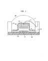
- FIG. 1is a schematic cross sectional view of a typical single LED packaged in accordance with the invention
- FIG. 2is a schematic cross sectional view of a typical array of LEDs packaged in accordance with the invention
- FIG. 3is a flow chart showing the steps in fabricating a white LED or LED array in accordance with the invention.
- FIG. 4is a schematic representation of a coating apparatus to facilitate coating the LEDs with phosphor particles.
- FIG. 1is a schematic cross section of an exemplary white light emitting diode (“white LED”) package assembly 100 for creating white light using a LED 101 and a fluorescent converting phosphor particle layer 102 .
- the LED die 101is placed on and advantageously wirebonded to the surface of a thermally conductive substrate 103 (preferably ceramic) inside a cavity 104 .
- An optical adhesive monolayer 105is placed on top of the LED body 101 and phosphor particles 106 forming layer 102 are adhered on top of the body.
- an optional encapsulation dome lens 107encapsulating the coated LED within the cavity 104 .
- the package assembly 100is composed of substrate 103 , a highly reflective layer 108 , usually silver, overlying the substrate and a conductive die attach material 109 .
- LED body 102is typically a nitride LED emitting blue or UV light, and can be connected using a wirebond 110 .
- LED body 101can have both P and N terminals on the top surface of the LED, in which case two wirebonds 110 will be attached from the top; or it can have both terminals on the bottom surface, using solder-bumping for attachment.
- LED body 101is advantageously covered with a first sticky transparent material 105 .
- the transparent material 105can be covered with a single layer 102 comprising phosphor particles 106 . Once deposited, the particles 106 can create a closed packed structured layer 102 film on top of sticky optical material 105 .
- Ceramic cavity 104can optionally then be sealed with a second transparent material 107 that advantageously forms a dome or lens in order to minimize total internal reflection (“TIR”).
- TIRtotal internal reflection
- FIG. 2illustrates a multiple LED array assembly 200 in which several LEDs 201 , are placed inside a ceramic cavity 202 similar to the cavity 104 described above.
- multiple LEDs 201can be attached on top of a highly conductive substrate 203 , as by conductive epoxy 204 .
- a transparent adhesive monolayer 205is placed on top of the multiple LED bodies 201 and a layer 206 of phosphor particles 207 is adhered overlying and over the sides of the bodies 201 .
- all LEDs 201can simultaneously be coated with the first tacky transparent material 205 .
- the particles 207 of the phosphor layer coatingcan attach to the tacky layer 205 creating a closed packed dense film layer 206 .
- assembly 200comprising wirebonded LEDs 201 can then optionally be sealed as by covering with a second transparent material 209 that can optionally create a dome or lens.
- the lensminimizes TIR.
- Substrate 203can be metal, ceramic, multilayer printed wire board, LTCC, HTCC or other suitable thermal conductor.
- the substrateadvantageously includes a heat sink. It can be electrically insulating or electrically conducting.
- Substrate 203advantageously comprises a highly thermally conductive metal such as copper, tungsten or molybdenum and/or a highly thermally conductive ceramic such as aluminum nitride (ALN), silicon carbide (SiC) or aluminum oxide (Al 2 O 3 ).
- ABNaluminum nitride
- SiCsilicon carbide
- Al 2 O 3aluminum oxide
- itcan be nickel-plated copper molybdenum copper clad.
- Metal powder mixturessuch as molybdenum copper, can be used in order to match the thermal expansion coefficient of the LED dies.
- a panelwill contain multiple cavities 202 , each with one or more LED assemblies.
- the panelis subsequently diced into individual elements 200 .
- a panelcan contain up to 24 elements (15.24 cm 2 ), an element (1.25 cm 2 ) can contain 7 cavities and a cavity can hold up to 12 (300 micron) LEDs.
- Reflective surface layer 210can be a coating of metal, such as silver, in a thick or thin film layer overlying the substrate 203 .
- LED dies 201can be attached to the package by conductive epoxy 204 , non-conductive epoxy or solder.
- connection between the LED and the substrateit is desirable for the connection between the LED and the substrate to have high thermal conductivity.
- Some LEDsare fabricated with both electrodes (anode P and cathode N) on the top surface. In such cases electrical connections can be made from the LED 201 to contacts on the substrate using wire bonds 211 .
- the wire bonds 211can be ball-wedge and wedge-wedge bonded gold or aluminum wires. Wires 211 can have different thicknesses.
- Other fabricationscan have one electrode on the top face of the LEDs 201 and the second electrode on the bottom. In this case, the connection between the LED 201 and the substrate 203 serves three purposes, first to mechanically attach the LED die to the substrate, second to provide a thermal path from the die into the substrate 203 , and third as an electrical connection to one of the LED electrodes.
- the tacky transparent material 205advantageously is a resin that has an index of refraction (IR) between the LED semiconductor material (3.0–2.8) and the fluorescent material particles 207 (1.77).
- IRindex of refraction
- the tackiness of the materialis due to a b-stage or partially cured resin. Tackiness is needed to adhere particles 207 .
- the material 205will also serve as a buffer layer as the photons exit the LED junctions and couple with the frequency converting phosphor 207 .
- the converting phosphorcan be particles of YAG:Ce. This structure will maximize the extraction of photons from LEDs 201 and produce a uniform color light distribution.
- the preferred tacky transparent materialsinclude but are not limited to partially cured silicones.
- the siliconescan include micro amino emulsions, elastomers, resins and cationics.
- Other useful polymeric resinsinclude butyrals, cellulosic, silicone polymers, acrylate compounds, high molecular weight polyethers, acrylic polymers, co-polymers, and multi-polymers.
- the index of refraction of the above-mentioned materialscan be tailored for optical matching.
- Embodiments 100 and 200depict frequency converting particles deposited on the sides and on top of the LED body.
- the particlesare advantageously single crystal from 5 to 19 micrometers in size preferably in a D:50 particle size distribution.
- Examples of such phosphor materials suitable for frequency conversioninclude but are not limited to garnet fluorescent material activated with cerium which can contain Y, Lu, Sc, La, Gd or Sm and an element from Al, Ga and In.
- Examples of non-garnet materialsinclude Sr 2 SiO 4 doped with Eu.
- organic semi-conducting phosphors for the near UV (360–410) and blue (>410 nm) useable as wavelength convertersare also used as wavelength converters. These new organic materials can be pulverized into particles and deposited using the techniques disclosed herein.
- the optional transparent encapsulant of assemblies 100 , 200can serve two purposes.
- the materialcan seal or encapsulate the cavity containing the coated LEDs, and it can create a lens that minimizes TIR.
- the index of refraction of the second materialpreferably lies between the fluorescent material particles (1.77) and air (1.0).
- the dome shaping of the lensis due to the thixotropic properties of the material.
- This materialis conveniently applied using a manifold syringe on automated equipment. It can alternatively be injection molded as by a steel mold.
- Useful materialsinclude butyrals, cellulosic polymers, silicone polymers, acrylate polymers, high molecular weight polyethers, and acrylic polymers, co-polymers, and multi-polymers. These materials can be tailored to have optically matched indices of refraction and appropriate viscosities.
- the illumination deviceis composed of at least one LED, at least one monolayer of transparent tacky material and at least one monolayer comprising frequency converting inorganic particles.
- the term “monolayer” as used hereinrefers to a thin film or coating that is less than 25 microns thick. Other layers that can be added include an amorphous film (no definite crystal structure) that conforms or molds to its surroundings. The surface of the LED crystal can be modified by deposition of a monolayer, which may change the reactivity of the LED surface with respect to particles. A surfactant can be used.
- Surfactantsare special organic molecules which are made up of two sections: the hydrophilic part (usually ionic or nonionic) which likes water and the hydrophobic part (usually a hydrocarbon chain) which likes oil.
- the interfacial layer formed as a result of thisis usually a monolayer and allows the particles to adhere to the LED. These monolayers can play an important role in the adhesion process.
- the monolayer of frequency converting particlescan be a layer of particles or an organic film layer that includes the particles.
- the adhesion mechanism that holds the particle layercan involve many mechanisms of particle-to-particle bonding. Among them are mechanical interlocking, molecular forces, Vanderwaals adhesion forces, capillary, electrostatic, magnetic, and free chemical forces. In most cases, the strength of the particle-to-particle particle bond depends on the contact pressure and surface area of contact between particles. The key is to create a dust or mist comprising the particles over the tacky film.
- the control of the powder qualitysuch as the particle size distribution, shape, and composition of the constituents has major influence on the development of the particle monolayer.
- Increasing the packing density in powdersis usually accomplished by filling the interstices between large particles with smaller particle sizes.
- the preferred particle distribution of the powdermeasured by a coulter counter with a 50 micron aperture, is:
- volume % Size 54.0 micron 25 8.3 micron 50 11.6 micron 75 14.8 micron 95 19.4 micron
- FIG. 3is a flow diagram showing the steps involved in an advantageous method of fabricating the white LEDs illumination devices.
- the first step, shown in Block A,is to provide a workpiece including one or more LEDs.
- a single LEDis advantageously mounted in a cavity on a substrate and electrically connected as shown in FIG. 1 .
- An array of LEDsis advantageously mounted and connected in a cavity on a panel as shown in FIG. 2 .
- the next stepis to mask the workpiece to cover areas of the workpiece which do not need to be coated with phosphor particles.
- the maskcan be a reusable mechanical mask e.g. stainless, beryllium copper or a non-reusable mask such as plastic or paper.
- the maskwill not be needed if the first optical material is selectively deposited such as by an automated dispensing machine using a syringe or pipette.
- the maskis also not needed if areas of the first transparent material are selectively made sticky, as, for example, by selectively exposing coated areas to a UV curing lamp.
- the third step, shown in Block C,is to coat a transparent layer of tacky material over the LED(s).
- a transparent layer of tacky materialIn order to create a monolayer of 5 to 25 microns in thickness, it is preferred to spin coat or spin remove the material using high rpm semiconductor spinning equipment. Panel wafers with mounted LEDs can be placed in the vertical position in order to maximize the removal of excess tacky material.
- the next step (Block D)is coating the fluorescent phosphor particles on the tacky first transparent material.
- a monolayercan be deposited by spraying the particles at high velocity onto workpiece wafers.
- the surface of the tacky materialwill adhere only one to a few of the particles in depth, creating a monolayer which is not sticky.
- the particle coatingis self-limiting. The particles will coat in all directions including the walls of the LED body as well as multiple contours.
- the next step (Block E)is to cure the tacky material to cross-link the polymers. Curing can be done by heat curing, e.g. UV curing or microwave curing, or by other curing methods.
- the 5 th step (Block F)which is optional, is to deposit the second transparent layer of encapsulating material overlying the coated LEDs inside the cavity or cavities.
- the next step shown in Block Gis to optionally dice the workpiece into a plurality of white LEDs or white LED arrays.
- a panel of coated and encapsulated LEDscan be diced into individual pieces using a dicing saw or a water jet.
- FIG. 4schematically illustrates coating apparatus 600 to facilitate coating white LED workpieces 618 with phosphor particles 620 .
- the apparatuscomprises an enclosed particle coating chamber 604 for receiving workpieces 618 to be coated.
- Chamber 604is coupled to a reservoir 608 of particles to be coated, a source of pressurized gas 605 through a Venturi Nozzle 613 and a recycling chamber 611 . It includes enclosed openings for coated wafers 618 to exit and unused particles to pass to the recycling chamber 611 .
- Air flow 605 from an outside source, such as a blower or high pressure air compressor,is inserted into apparatus 600 .
- the air pressurecan be approximately 100 PSI on an intake hose or tube.
- the aircompresses into a nozzle 613 where the Venturi effect and the difference in pressures, forces the particles to the air stream from reservoir 608 .
- the force of the air flowis advantageously large enough to break any agglomerates in the phosphor powder, thus fluidizing the particles and dispersing them at high velocity.
- An air velocity of 10 to 15 feet per secondis sufficient for this purpose.
- Mechanical dispersal of particlesprecludes the need for chemical dispersants for the phosphor particles. This is particularly advantageous since introduction of these additives can induce unwanted color nuances.
- the coating processbegins in the coating chamber 604 and deposits particles 620 randomly on top of the wafer 618 .
- the incoming panel feedtransports wafers 617 into coating chamber 604 .
- Wafer 618is shown in position to be coated.
- Excess particles 620not deposited into the wafer, move to the bottom of the chamber 619 and can be re-circulated by flow 604 into the system by back feed tube 607 .
- Back air pressure 609can be created by vacuum source 601 .
- Flow 609created by suction caused by vacuum source 601 , passes through a powder filter 610 .
- Filter 610can be paper or preferably sintered metal powder, which gets purged by a purging valve 602 , that is bridged from the incoming air stream 603 .
- the recycled particlescan then drop by gravity into the bottom of the cyclone chamber 611 and into a screw feed 614 .
- Screw feed 614can be controlled by stepping motor 612 . The screw feed can then move the phosphor particles back into the nozzle 613 by the Venturi effect and the cycle repeats again.
- Substrate MaterialCopper Molybdenum Copper (Sumitomo Inc.)LED: UltraBrightTM InGaN LED (Cree Inc.)
- First Optical MaterialNYOGEL OKT-0451 2 part silicone heat curable (NYE optical)Frequency Converting Material: YAG:Ce Phosphor (Phosphor Technologies UK)Second Optical Material: LED Encapsulant 9616 Dymax Corp
- Substrate MaterialCopper Tungsten (Marketech Int. INC) LED: InGaN/GaN Blue LED's 3.3 (Epistar Corporation)
- First Optical MaterialSylguard—2 part silicone heat curable (Dow Corning INC)Frequency Converting Material: YAG:Gd Phosphor (Phosphor Tech. USA)Second Optical Material: LS-6257 Encapsulant (Light Span Corp)
- An array of LEDs plus a mono-layer of fluorescent materialcan be used to create a light source having a uniform white light distribution, thus minimizing the “Halo Effect”.
- the “Halo Effect” or bleed-through effectoccurs because the light from the blue LED is directional while the yellow/amber from the phosphor radiates over 2 ⁇ solid angle.
- an observer looking at a prior art LED from the sidecan see a color that appears multi-color, not white.
- the single layer of fluorescent material as per the inventive techniquecan coat multiple blue LEDs and create a uniform white light distribution in all directions.
- Photonic emission recombination of wavelengthscan be accomplished by an interaction between the host and the activator.
- the recombinationcan be attributed to the presence of an excited outer shell of the phosphor dopant ion.
- the emission band of the phosphor particlessingle crystal structure shifts of to a longer wavelength as the photon crosses the fluorescent material.
- the inventioncreates an efficient blue LED plus phosphor white light by minimizing the number of times that the photons have to pass through the wavelength converting material.
- the blue LED approachis not limited to only one wavelength converting phosphor. It can be used with a two or three component phosphor system to generate high quality white. This option may use an ultra violet (“UV”) LED to excite several phosphors to simultaneously generate different colors. Multiple phosphors are preferred in order to increase the Color Rendering Index (“CRI”) of the light. Using such techniques, high color rendering indices similar to fluorescent lamps can be realized.
- the present inventioncan create a homogenous mix of the multiple phosphors by mechanically mixing phosphors at high speeds.
- Scattering lossescan be attributed to encounters with a particle or molecule as the electromagnetic wave propagates. The net effect is that the incident wave becomes partially re-radiated in different directions and hence loses intensity in its original direction of propagation.
- a single layer of fluorescent material in the form of a thin film layer of particlesis preferred. Contrary to previous methods, the phosphor particles are not mixed in binders or epoxies. No matter how thin the layer is deposited, multiple particles in a binder will contribute to an increase in scattering losses. The applicant discloses a method in which a self limiting single layer of particles is attached to an optical dielectric film.
- Optically matched dielectric materialis critical for the reduction of total internal reflection (TIR).
- TIRtotal internal reflection
- the preferred embodimentwill coat the LED diode body with material having refractive indices that allow for maximum ray extraction from the semiconductor materials. At the same time the dielectric coating will allow particles of fluorescent material to attach to its surface creating a uniform conformal layer around its body.
- the coating methodincludes a thin film layer of optically matched tacky material that is deposited prior to a uniform particles coating. The whole process occurs with the LED diodes already mounted and wirebonded to the thermal package inside the cavity.
Landscapes
- Led Device Packages (AREA)
Abstract
Description
| Volume % | Size | ||
| 5 | 4.0 micron | ||
| 25 | 8.3 micron | ||
| 50 | 11.6 micron | ||
| 75 | 14.8 micron | ||
| 95 | 19.4 micron | ||
Claims (28)
Priority Applications (2)
| Application Number | Priority Date | Filing Date | Title |
|---|---|---|---|
| US10/822,236US7157745B2 (en) | 2004-04-09 | 2004-04-09 | Illumination devices comprising white light emitting diodes and diode arrays and method and apparatus for making them |
| US11/445,611US20070013057A1 (en) | 2003-05-05 | 2006-06-02 | Multicolor LED assembly with improved color mixing |
Applications Claiming Priority (1)
| Application Number | Priority Date | Filing Date | Title |
|---|---|---|---|
| US10/822,236US7157745B2 (en) | 2004-04-09 | 2004-04-09 | Illumination devices comprising white light emitting diodes and diode arrays and method and apparatus for making them |
Related Child Applications (1)
| Application Number | Title | Priority Date | Filing Date |
|---|---|---|---|
| US11/445,611Continuation-In-PartUS20070013057A1 (en) | 2003-05-05 | 2006-06-02 | Multicolor LED assembly with improved color mixing |
Publications (2)
| Publication Number | Publication Date |
|---|---|
| US20050224830A1 US20050224830A1 (en) | 2005-10-13 |
| US7157745B2true US7157745B2 (en) | 2007-01-02 |
Family
ID=35059686
Family Applications (1)
| Application Number | Title | Priority Date | Filing Date |
|---|---|---|---|
| US10/822,236Expired - LifetimeUS7157745B2 (en) | 2003-05-05 | 2004-04-09 | Illumination devices comprising white light emitting diodes and diode arrays and method and apparatus for making them |
Country Status (1)
| Country | Link |
|---|---|
| US (1) | US7157745B2 (en) |
Cited By (73)
| Publication number | Priority date | Publication date | Assignee | Title |
|---|---|---|---|---|
| US20050280354A1 (en)* | 2004-06-16 | 2005-12-22 | Shin-Lung Liu | Light emitting diode |
| US20060022211A1 (en)* | 2004-07-30 | 2006-02-02 | Yasushi Yatsuda | LED lamp for light source of lighting device |
| US20060171151A1 (en)* | 2005-02-03 | 2006-08-03 | Samsung Electro-Mechanics Co., Ltd. | Side-emission typy LED package |
| US20070004065A1 (en)* | 2005-06-30 | 2007-01-04 | 3M Innovative Properties Company | Phosphor tape article |
| US20070001182A1 (en)* | 2005-06-30 | 2007-01-04 | 3M Innovative Properties Company | Structured phosphor tape article |
| US20070241355A1 (en)* | 2006-04-13 | 2007-10-18 | Chua Janet B Y | System and method for enhancing light emissions from light packages by adjusting the index of refraction at the surface of the encapsulation material |
| US20080023712A1 (en)* | 2006-01-16 | 2008-01-31 | Philips Lumileds Lighting Company, Llc | Phosphor Converted Light Emitting Device |
| US20080121918A1 (en)* | 2006-11-15 | 2008-05-29 | The Regents Of The University Of California | High light extraction efficiency sphere led |
| US20080128730A1 (en)* | 2006-11-15 | 2008-06-05 | The Regents Of The University Of California | Textured phosphor conversion layer light emitting diode |
| US20080157103A1 (en)* | 2005-10-28 | 2008-07-03 | Philips Lumileds Lighting Company, Llc | Laminating Encapsulant Film Containing Phosphor Over LEDs |
| US20080217631A1 (en)* | 2007-03-07 | 2008-09-11 | Everlight Electronics Co., Ltd. | Semiconductor light emitting apparatus and the manufacturing method thereof |
| EP1973325A1 (en) | 2007-03-20 | 2008-09-24 | Xerox Corporation | Document Illuminator with LED-Driven Phosphor |
| US20080237614A1 (en)* | 2007-03-29 | 2008-10-02 | Takuro Ishikura | Semiconductor light-emitting device |
| US20090121250A1 (en)* | 2006-11-15 | 2009-05-14 | Denbaars Steven P | High light extraction efficiency light emitting diode (led) using glass packaging |
| US20090212690A1 (en)* | 2007-12-18 | 2009-08-27 | Lumimove, Inc., D/B/A Crosslink | Flexible electroluminescent devices and systems |
| US20090236619A1 (en)* | 2008-03-19 | 2009-09-24 | Arpan Chakroborty | Light Emitting Diodes with Light Filters |
| US20090244923A1 (en)* | 2006-04-26 | 2009-10-01 | Koninklijke Philips Electronics N.V. | Light delivery device with improved conversion element |
| US20090267086A1 (en)* | 2008-04-29 | 2009-10-29 | Wei Shi | Thermal Management For LED |
| US20090296389A1 (en)* | 2008-05-30 | 2009-12-03 | Chia-Liang Hsu | Light source module, related light bar and related liquid crystal display |
| US20100025718A1 (en)* | 2008-07-31 | 2010-02-04 | Wei Shi | Top contact LED thermal management |
| WO2010030699A1 (en)* | 2008-09-10 | 2010-03-18 | Bridgelux, Inc. | Phosphor layer arrangement for use with light emitting diodes |
| US20100110692A1 (en)* | 2007-10-15 | 2010-05-06 | Foshan Nationstar Optoelectronics Co., Ltd. | Structure of heat dissipation substrate for power led and a device manufactured by it |
| US20100200876A1 (en)* | 2009-02-06 | 2010-08-12 | Everlight Electronics Co., Ltd. | Multi-chip light emitting diode and method for fabricating the same |
| US20100213487A1 (en)* | 2009-02-24 | 2010-08-26 | Advanced Optoelectronic Technology, Inc. | Side-emitting led package and manufacturing method of the same |
| US20100295068A1 (en)* | 2007-08-27 | 2010-11-25 | Bu Wan Seo | Light emitting device package and lighting apparatus using the same |
| US20110176316A1 (en)* | 2011-03-18 | 2011-07-21 | Phipps J Michael | Semiconductor lamp with thermal handling system |
| US20110193473A1 (en)* | 2011-03-18 | 2011-08-11 | Sanders Chad N | White light lamp using semiconductor light emitter(s) and remotely deployed phosphor(s) |
| US20120007119A1 (en)* | 2010-07-08 | 2012-01-12 | Shin-Etsu Chemical Co., Ltd. | Light-emitting semiconductor device, mounted substrate, and fabrication method thereof |
| US20120074446A1 (en)* | 2010-09-29 | 2012-03-29 | Seoul Semiconductor Co., Ltd. | Phosphor sheet, light-emitting device having the phosphor sheet and method of manufacturing the same |
| CN102593340A (en)* | 2012-03-05 | 2012-07-18 | 清华大学 | White light LED luminescence apparatus |
| US8253336B2 (en) | 2010-07-23 | 2012-08-28 | Biological Illumination, Llc | LED lamp for producing biologically-corrected light |
| US20120235188A1 (en)* | 2011-03-15 | 2012-09-20 | Avago Technologies Ecbu Ip (Singapore) Pte. Ltd. | Method and Apparatus for a Flat Top Light Source |
| US8324808B2 (en) | 2010-07-23 | 2012-12-04 | Biological Illumination, Llc | LED lamp for producing biologically-corrected light |
| US20120313120A1 (en)* | 2011-06-09 | 2012-12-13 | Albeo Technologies, Inc. | Method For Depositing A Phosphor Layer On LEDs, And Apparatus Made Thereby |
| US20130001636A1 (en)* | 2011-06-28 | 2013-01-03 | Aceplux Optotech Inc. | Light-emitting diode and method for forming the same |
| TWI382566B (en)* | 2008-11-07 | 2013-01-11 | Nat Univ Chung Hsing | And a light-emitting diode chip having an adhesive layer of reflectionable light |
| WO2013051281A1 (en) | 2011-10-07 | 2013-04-11 | コニカミノルタアドバンストレイヤー株式会社 | Led device manufacturing method and fluorescent material-dispersed solution used in same |
| US20130200398A1 (en)* | 2012-02-07 | 2013-08-08 | Chih-Ming Wang | Light emitting diode with wavelength conversion layer |
| US8680457B2 (en) | 2012-05-07 | 2014-03-25 | Lighting Science Group Corporation | Motion detection system and associated methods having at least one LED of second set of LEDs to vary its voltage |
| US8686641B2 (en) | 2011-12-05 | 2014-04-01 | Biological Illumination, Llc | Tunable LED lamp for producing biologically-adjusted light |
| US8743023B2 (en) | 2010-07-23 | 2014-06-03 | Biological Illumination, Llc | System for generating non-homogenous biologically-adjusted light and associated methods |
| US20140151630A1 (en)* | 2012-12-04 | 2014-06-05 | Feng-Hsu Fan | Protection for the epitaxial structure of metal devices |
| US8754832B2 (en) | 2011-05-15 | 2014-06-17 | Lighting Science Group Corporation | Lighting system for accenting regions of a layer and associated methods |
| US8760370B2 (en) | 2011-05-15 | 2014-06-24 | Lighting Science Group Corporation | System for generating non-homogenous light and associated methods |
| US8761447B2 (en) | 2010-11-09 | 2014-06-24 | Biological Illumination, Llc | Sustainable outdoor lighting system for use in environmentally photo-sensitive area |
| TWI449221B (en)* | 2009-01-16 | 2014-08-11 | Everlight Electronics Co Ltd | Light-emitting diode package structure and manufacturing method thereof |
| US8803412B2 (en) | 2011-03-18 | 2014-08-12 | Abl Ip Holding Llc | Semiconductor lamp |
| US8841864B2 (en) | 2011-12-05 | 2014-09-23 | Biological Illumination, Llc | Tunable LED lamp for producing biologically-adjusted light |
| US8866414B2 (en) | 2011-12-05 | 2014-10-21 | Biological Illumination, Llc | Tunable LED lamp for producing biologically-adjusted light |
| US8901850B2 (en) | 2012-05-06 | 2014-12-02 | Lighting Science Group Corporation | Adaptive anti-glare light system and associated methods |
| CN104364922A (en)* | 2012-06-06 | 2015-02-18 | 日立化成株式会社 | Optical semiconductor device |
| US8963450B2 (en) | 2011-12-05 | 2015-02-24 | Biological Illumination, Llc | Adaptable biologically-adjusted indirect lighting device and associated methods |
| USD723729S1 (en) | 2013-03-15 | 2015-03-03 | Lighting Science Group Corporation | Low bay luminaire |
| US9006987B2 (en) | 2012-05-07 | 2015-04-14 | Lighting Science Group, Inc. | Wall-mountable luminaire and associated systems and methods |
| US9024536B2 (en) | 2011-12-05 | 2015-05-05 | Biological Illumination, Llc | Tunable LED lamp for producing biologically-adjusted light and associated methods |
| US20150200340A1 (en)* | 2014-01-14 | 2015-07-16 | Kabushiki Kaisha Toshiba | Light-emitting device |
| US9173269B2 (en) | 2011-05-15 | 2015-10-27 | Lighting Science Group Corporation | Lighting system for accentuating regions of a layer and associated methods |
| US9174067B2 (en) | 2012-10-15 | 2015-11-03 | Biological Illumination, Llc | System for treating light treatable conditions and associated methods |
| US9220202B2 (en) | 2011-12-05 | 2015-12-29 | Biological Illumination, Llc | Lighting system to control the circadian rhythm of agricultural products and associated methods |
| US9289574B2 (en) | 2011-12-05 | 2016-03-22 | Biological Illumination, Llc | Three-channel tuned LED lamp for producing biologically-adjusted light |
| US9347655B2 (en) | 2013-03-11 | 2016-05-24 | Lighting Science Group Corporation | Rotatable lighting device |
| US9402294B2 (en) | 2012-05-08 | 2016-07-26 | Lighting Science Group Corporation | Self-calibrating multi-directional security luminaire and associated methods |
| US9532423B2 (en) | 2010-07-23 | 2016-12-27 | Lighting Science Group Corporation | System and methods for operating a lighting device |
| US20160380162A1 (en)* | 2015-06-26 | 2016-12-29 | Everlight Electronics Co., Ltd. | Light Emitting Device And Manufacturing Method Thereof |
| US9681522B2 (en) | 2012-05-06 | 2017-06-13 | Lighting Science Group Corporation | Adaptive light system and associated methods |
| US9693414B2 (en) | 2011-12-05 | 2017-06-27 | Biological Illumination, Llc | LED lamp for producing biologically-adjusted light |
| US9748449B2 (en) | 2003-07-04 | 2017-08-29 | Epistar Corporation | Optoelectronic system |
| US9827439B2 (en) | 2010-07-23 | 2017-11-28 | Biological Illumination, Llc | System for dynamically adjusting circadian rhythm responsive to scheduled events and associated methods |
| US20190319169A1 (en)* | 2017-08-11 | 2019-10-17 | Xiamen San'an Optoelectronics Co., Ltd. | Light emitting device and method for manufacturing the same |
| US10454010B1 (en) | 2006-12-11 | 2019-10-22 | The Regents Of The University Of California | Transparent light emitting diodes |
| US11562989B2 (en)* | 2018-09-25 | 2023-01-24 | Nichia Corporation | Light-emitting device and method for manufacturing same |
| US11592166B2 (en) | 2020-05-12 | 2023-02-28 | Feit Electric Company, Inc. | Light emitting device having improved illumination and manufacturing flexibility |
| US11876042B2 (en) | 2020-08-03 | 2024-01-16 | Feit Electric Company, Inc. | Omnidirectional flexible light emitting device |
Families Citing this family (117)
| Publication number | Priority date | Publication date | Assignee | Title |
|---|---|---|---|---|
| JP5004410B2 (en)* | 2004-04-26 | 2012-08-22 | Towa株式会社 | Optical element resin sealing molding method and resin sealing molding apparatus |
| JP5128047B2 (en)* | 2004-10-07 | 2013-01-23 | Towa株式会社 | Optical device and optical device production method |
| US20060097385A1 (en)* | 2004-10-25 | 2006-05-11 | Negley Gerald H | Solid metal block semiconductor light emitting device mounting substrates and packages including cavities and heat sinks, and methods of packaging same |
| US7772609B2 (en)* | 2004-10-29 | 2010-08-10 | Ledengin, Inc. (Cayman) | LED package with structure and materials for high heat dissipation |
| US9929326B2 (en) | 2004-10-29 | 2018-03-27 | Ledengin, Inc. | LED package having mushroom-shaped lens with volume diffuser |
| US8324641B2 (en)* | 2007-06-29 | 2012-12-04 | Ledengin, Inc. | Matrix material including an embedded dispersion of beads for a light-emitting device |
| US8816369B2 (en) | 2004-10-29 | 2014-08-26 | Led Engin, Inc. | LED packages with mushroom shaped lenses and methods of manufacturing LED light-emitting devices |
| US7670872B2 (en)* | 2004-10-29 | 2010-03-02 | LED Engin, Inc. (Cayman) | Method of manufacturing ceramic LED packages |
| US8134292B2 (en)* | 2004-10-29 | 2012-03-13 | Ledengin, Inc. | Light emitting device with a thermal insulating and refractive index matching material |
| US7473933B2 (en)* | 2004-10-29 | 2009-01-06 | Ledengin, Inc. (Cayman) | High power LED package with universal bonding pads and interconnect arrangement |
| US20060214577A1 (en)* | 2005-03-26 | 2006-09-28 | Lorraine Byrne | Depositing of powdered luminescent material onto substrate of electroluminescent lamp |
| TW200704283A (en) | 2005-05-27 | 2007-01-16 | Lamina Ceramics Inc | Solid state LED bridge rectifier light engine |
| US7985357B2 (en)* | 2005-07-12 | 2011-07-26 | Towa Corporation | Method of resin-sealing and molding an optical device |
| KR100763894B1 (en)* | 2006-03-21 | 2007-10-05 | 삼성에스디아이 주식회사 | Manufacturing method of display device using LED chip |
| EP3422425B1 (en)* | 2006-04-24 | 2022-02-23 | CreeLED, Inc. | Side-view surface mount white led |
| WO2007139781A2 (en) | 2006-05-23 | 2007-12-06 | Cree Led Lighting Solutions, Inc. | Lighting device |
| JP4984824B2 (en)* | 2006-10-26 | 2012-07-25 | 豊田合成株式会社 | Light emitting device |
| DE102007018837A1 (en)* | 2007-03-26 | 2008-10-02 | Osram Opto Semiconductors Gmbh | Method for producing a luminescence diode chip and luminescence diode chip |
| US20080283864A1 (en)* | 2007-05-16 | 2008-11-20 | Letoquin Ronan P | Single Crystal Phosphor Light Conversion Structures for Light Emitting Devices |
| JP5158472B2 (en)* | 2007-05-24 | 2013-03-06 | スタンレー電気株式会社 | Semiconductor light emitting device |
| JP4869165B2 (en)* | 2007-06-28 | 2012-02-08 | 昭和電工株式会社 | Method for manufacturing light emitting device |
| WO2009054177A1 (en)* | 2007-10-24 | 2009-04-30 | Sharp Kabushiki Kaisha | Illuminating device for display device, display device, and television receiver |
| US8058088B2 (en) | 2008-01-15 | 2011-11-15 | Cree, Inc. | Phosphor coating systems and methods for light emitting structures and packaged light emitting diodes including phosphor coating |
| US8940561B2 (en)* | 2008-01-15 | 2015-01-27 | Cree, Inc. | Systems and methods for application of optical materials to optical elements |
| US10008637B2 (en) | 2011-12-06 | 2018-06-26 | Cree, Inc. | Light emitter devices and methods with reduced dimensions and improved light output |
| US7766514B2 (en)* | 2008-06-05 | 2010-08-03 | Hon-Wen Chen | Light emitting diode lamp with high heat-dissipation capacity |
| KR101506264B1 (en)* | 2008-06-13 | 2015-03-30 | 삼성전자주식회사 | Light emitting device, light emitting device, and manufacturing method of the light emitting device |
| US7955875B2 (en)* | 2008-09-26 | 2011-06-07 | Cree, Inc. | Forming light emitting devices including custom wavelength conversion structures |
| US8075165B2 (en)* | 2008-10-14 | 2011-12-13 | Ledengin, Inc. | Total internal reflection lens and mechanical retention and locating device |
| US20100117106A1 (en)* | 2008-11-07 | 2010-05-13 | Ledengin, Inc. | Led with light-conversion layer |
| KR101039957B1 (en)* | 2008-11-18 | 2011-06-09 | 엘지이노텍 주식회사 | Light emitting device and display device having same |
| US8507300B2 (en)* | 2008-12-24 | 2013-08-13 | Ledengin, Inc. | Light-emitting diode with light-conversion layer |
| KR101496846B1 (en)* | 2008-12-24 | 2015-03-02 | 삼성디스플레이 주식회사 | Display device comprising organic light emitting transistor and method of fabricating the same |
| CN101771025A (en)* | 2008-12-26 | 2010-07-07 | 富准精密工业(深圳)有限公司 | led |
| KR101028316B1 (en) | 2009-02-13 | 2011-04-12 | 엘지이노텍 주식회사 | Light emitting diode package |
| US8247886B1 (en) | 2009-03-09 | 2012-08-21 | Soraa, Inc. | Polarization direction of optical devices using selected spatial configurations |
| US8299473B1 (en) | 2009-04-07 | 2012-10-30 | Soraa, Inc. | Polarized white light devices using non-polar or semipolar gallium containing materials and transparent phosphors |
| US8912023B2 (en) | 2009-04-08 | 2014-12-16 | Ledengin, Inc. | Method and system for forming LED light emitters |
| US7985000B2 (en)* | 2009-04-08 | 2011-07-26 | Ledengin, Inc. | Lighting apparatus having multiple light-emitting diodes with individual light-conversion layers |
| CN101894901B (en) | 2009-04-08 | 2013-11-20 | 硅谷光擎 | Package for multiple light emitting diodes |
| US8598793B2 (en) | 2011-05-12 | 2013-12-03 | Ledengin, Inc. | Tuning of emitter with multiple LEDs to a single color bin |
| US8323998B2 (en)* | 2009-05-15 | 2012-12-04 | Achrolux Inc. | Methods and apparatus for forming uniform layers of phosphor material on an LED encapsulation structure |
| US8791499B1 (en) | 2009-05-27 | 2014-07-29 | Soraa, Inc. | GaN containing optical devices and method with ESD stability |
| WO2011004637A1 (en)* | 2009-07-06 | 2011-01-13 | シャープ株式会社 | Illumination device, display device, and television receiver |
| US9000466B1 (en) | 2010-08-23 | 2015-04-07 | Soraa, Inc. | Methods and devices for light extraction from a group III-nitride volumetric LED using surface and sidewall roughening |
| US8207554B2 (en) | 2009-09-11 | 2012-06-26 | Soraa, Inc. | System and method for LED packaging |
| US8933644B2 (en) | 2009-09-18 | 2015-01-13 | Soraa, Inc. | LED lamps with improved quality of light |
| US9293644B2 (en) | 2009-09-18 | 2016-03-22 | Soraa, Inc. | Power light emitting diode and method with uniform current density operation |
| JP5359732B2 (en)* | 2009-09-18 | 2013-12-04 | 豊田合成株式会社 | Method for manufacturing light emitting device |
| US9583678B2 (en) | 2009-09-18 | 2017-02-28 | Soraa, Inc. | High-performance LED fabrication |
| CN102630349B (en) | 2009-09-18 | 2017-06-13 | 天空公司 | Power light emitting diode and method of operating with current density |
| US9293667B2 (en) | 2010-08-19 | 2016-03-22 | Soraa, Inc. | System and method for selected pump LEDs with multiple phosphors |
| US8575642B1 (en) | 2009-10-30 | 2013-11-05 | Soraa, Inc. | Optical devices having reflection mode wavelength material |
| US8303141B2 (en)* | 2009-12-17 | 2012-11-06 | Ledengin, Inc. | Total internal reflection lens with integrated lamp cover |
| KR20110087579A (en)* | 2010-01-26 | 2011-08-03 | 삼성엘이디 주식회사 | LED module and backlight unit having the same |
| US10147850B1 (en) | 2010-02-03 | 2018-12-04 | Soraa, Inc. | System and method for providing color light sources in proximity to predetermined wavelength conversion structures |
| US8905588B2 (en) | 2010-02-03 | 2014-12-09 | Sorra, Inc. | System and method for providing color light sources in proximity to predetermined wavelength conversion structures |
| US20110186874A1 (en)* | 2010-02-03 | 2011-08-04 | Soraa, Inc. | White Light Apparatus and Method |
| US8740413B1 (en) | 2010-02-03 | 2014-06-03 | Soraa, Inc. | System and method for providing color light sources in proximity to predetermined wavelength conversion structures |
| US8858022B2 (en) | 2011-05-05 | 2014-10-14 | Ledengin, Inc. | Spot TIR lens system for small high-power emitter |
| US9345095B2 (en) | 2010-04-08 | 2016-05-17 | Ledengin, Inc. | Tunable multi-LED emitter module |
| US9080729B2 (en) | 2010-04-08 | 2015-07-14 | Ledengin, Inc. | Multiple-LED emitter for A-19 lamps |
| US8293551B2 (en) | 2010-06-18 | 2012-10-23 | Soraa, Inc. | Gallium and nitrogen containing triangular or diamond-shaped configuration for optical devices |
| US9450143B2 (en) | 2010-06-18 | 2016-09-20 | Soraa, Inc. | Gallium and nitrogen containing triangular or diamond-shaped configuration for optical devices |
| WO2012043896A1 (en)* | 2010-09-27 | 2012-04-05 | 에이엠티 주식회사 | Quantification device and quantification method thereof |
| US20120097985A1 (en)* | 2010-10-21 | 2012-04-26 | Wen-Huang Liu | Light Emitting Diode (LED) Package And Method Of Fabrication |
| US8541951B1 (en) | 2010-11-17 | 2013-09-24 | Soraa, Inc. | High temperature LED system using an AC power source |
| US8896235B1 (en) | 2010-11-17 | 2014-11-25 | Soraa, Inc. | High temperature LED system using an AC power source |
| US8786053B2 (en) | 2011-01-24 | 2014-07-22 | Soraa, Inc. | Gallium-nitride-on-handle substrate materials and devices and method of manufacture |
| US9166126B2 (en) | 2011-01-31 | 2015-10-20 | Cree, Inc. | Conformally coated light emitting devices and methods for providing the same |
| US9508904B2 (en) | 2011-01-31 | 2016-11-29 | Cree, Inc. | Structures and substrates for mounting optical elements and methods and devices for providing the same background |
| TW201251140A (en) | 2011-01-31 | 2012-12-16 | Cree Inc | High brightness light emitting diode (LED) packages, systems and methods with improved resin filling and high adhesion |
| CN103348496A (en)* | 2011-02-07 | 2013-10-09 | 克利公司 | Components and methods for light emitting diode (LED) lighting |
| US8513900B2 (en) | 2011-05-12 | 2013-08-20 | Ledengin, Inc. | Apparatus for tuning of emitter with multiple LEDs to a single color bin |
| JP2014525146A (en) | 2011-07-21 | 2014-09-25 | クリー インコーポレイテッド | Light emitting device, package, component, and method for improved chemical resistance and related methods |
| US10211380B2 (en)* | 2011-07-21 | 2019-02-19 | Cree, Inc. | Light emitting devices and components having improved chemical resistance and related methods |
| US10686107B2 (en) | 2011-07-21 | 2020-06-16 | Cree, Inc. | Light emitter devices and components with improved chemical resistance and related methods |
| US8686431B2 (en) | 2011-08-22 | 2014-04-01 | Soraa, Inc. | Gallium and nitrogen containing trilateral configuration for optical devices |
| US9488324B2 (en) | 2011-09-02 | 2016-11-08 | Soraa, Inc. | Accessories for LED lamp systems |
| US8685808B2 (en)* | 2011-09-28 | 2014-04-01 | Taiwan Semiconductor Manufacturing Company, Ltd. | Semiconductor device fabrication method |
| US9236379B2 (en) | 2011-09-28 | 2016-01-12 | Taiwan Semiconductor Manufacturing Company, Ltd. | Semiconductor device and fabrication method thereof |
| US8912025B2 (en) | 2011-11-23 | 2014-12-16 | Soraa, Inc. | Method for manufacture of bright GaN LEDs using a selective removal process |
| US9496466B2 (en) | 2011-12-06 | 2016-11-15 | Cree, Inc. | Light emitter devices and methods, utilizing light emitting diodes (LEDs), for improved light extraction |
| TW201327926A (en)* | 2011-12-30 | 2013-07-01 | Ind Tech Res Inst | Light conversion structure and the light emitting device packaging structure using the same |
| US9343441B2 (en) | 2012-02-13 | 2016-05-17 | Cree, Inc. | Light emitter devices having improved light output and related methods |
| US9240530B2 (en) | 2012-02-13 | 2016-01-19 | Cree, Inc. | Light emitter devices having improved chemical and physical resistance and related methods |
| US11032884B2 (en) | 2012-03-02 | 2021-06-08 | Ledengin, Inc. | Method for making tunable multi-led emitter module |
| JP2015509669A (en) | 2012-03-06 | 2015-03-30 | ソラア インコーポレーテッドSoraa Inc. | Light emitting diode with low refractive index material layer to reduce guided light effect |
| US9897284B2 (en) | 2012-03-28 | 2018-02-20 | Ledengin, Inc. | LED-based MR16 replacement lamp |
| US8985794B1 (en) | 2012-04-17 | 2015-03-24 | Soraa, Inc. | Providing remote blue phosphors in an LED lamp |
| US20130328074A1 (en)* | 2012-06-11 | 2013-12-12 | Cree, Inc. | Led package with multiple element light source and encapsulant having planar surfaces |
| US8971368B1 (en) | 2012-08-16 | 2015-03-03 | Soraa Laser Diode, Inc. | Laser devices having a gallium and nitrogen containing semipolar surface orientation |
| US9978904B2 (en) | 2012-10-16 | 2018-05-22 | Soraa, Inc. | Indium gallium nitride light emitting devices |
| US8802471B1 (en) | 2012-12-21 | 2014-08-12 | Soraa, Inc. | Contacts for an n-type gallium and nitrogen substrate for optical devices |
| US9761763B2 (en) | 2012-12-21 | 2017-09-12 | Soraa, Inc. | Dense-luminescent-materials-coated violet LEDs |
| US9644817B2 (en)* | 2013-02-09 | 2017-05-09 | Hisham Menkara | Phosphor sheets |
| US9234801B2 (en) | 2013-03-15 | 2016-01-12 | Ledengin, Inc. | Manufacturing method for LED emitter with high color consistency |
| CN103280509A (en)* | 2013-05-24 | 2013-09-04 | 北京半导体照明科技促进中心 | Powder coating method and method using same for coating LED (light emitting diode) fluorescent powder |
| US8994033B2 (en) | 2013-07-09 | 2015-03-31 | Soraa, Inc. | Contacts for an n-type gallium and nitrogen substrate for optical devices |
| US9589852B2 (en)* | 2013-07-22 | 2017-03-07 | Cree, Inc. | Electrostatic phosphor coating systems and methods for light emitting structures and packaged light emitting diodes including phosphor coating |
| US9419189B1 (en) | 2013-11-04 | 2016-08-16 | Soraa, Inc. | Small LED source with high brightness and high efficiency |
| JP6152801B2 (en)* | 2014-01-21 | 2017-06-28 | 豊田合成株式会社 | Light emitting device and manufacturing method thereof |
| US9406654B2 (en) | 2014-01-27 | 2016-08-02 | Ledengin, Inc. | Package for high-power LED devices |
| CN107004677B (en) | 2014-11-26 | 2020-08-25 | 硅谷光擎 | Compact transmitter for warm dimming and color-tunable lamps |
| US9530943B2 (en) | 2015-02-27 | 2016-12-27 | Ledengin, Inc. | LED emitter packages with high CRI |
| CN105990496B (en)* | 2015-03-04 | 2018-11-16 | 光宝光电(常州)有限公司 | LED encapsulation structure and its manufacturing method |
| US10219345B2 (en) | 2016-11-10 | 2019-02-26 | Ledengin, Inc. | Tunable LED emitter with continuous spectrum |
| KR102831200B1 (en)* | 2017-02-02 | 2025-07-10 | 서울반도체 주식회사 | Light emitting diode package |
| TWI603649B (en)* | 2017-02-07 | 2017-10-21 | 國立中山大學 | Method and device for improving luminous intensity of ultraviolet light emitting diode |
| US11177417B2 (en) | 2017-02-13 | 2021-11-16 | Nichia Corporation | Light emitting device including phosphor layer with protrusions and recesses and method for manufacturing same |
| JP6645486B2 (en) | 2017-02-13 | 2020-02-14 | 日亜化学工業株式会社 | Light emitting device and method of manufacturing the same |
| TW201915818A (en)* | 2017-10-05 | 2019-04-16 | 香港商印芯科技股份有限公司 | Optical identification module |
| JP6773063B2 (en)* | 2018-02-22 | 2020-10-21 | 日亜化学工業株式会社 | Method of forming a translucent member |
| US10575374B2 (en) | 2018-03-09 | 2020-02-25 | Ledengin, Inc. | Package for flip-chip LEDs with close spacing of LED chips |
| US11362243B2 (en)* | 2019-10-09 | 2022-06-14 | Lumileds Llc | Optical coupling layer to improve output flux in LEDs |
| CN110797449A (en)* | 2019-11-05 | 2020-02-14 | 鸿利智汇集团股份有限公司 | LED package and packaging method thereof |
| WO2025005073A1 (en)* | 2023-06-30 | 2025-01-02 | 日亜化学工業株式会社 | Light emitting device and method for manufacturing light emitting device |
Citations (30)
| Publication number | Priority date | Publication date | Assignee | Title |
|---|---|---|---|---|
| US4902567A (en)* | 1987-12-31 | 1990-02-20 | Loctite Luminescent Systems, Inc. | Electroluminescent lamp devices using monolayers of electroluminescent materials |
| US5441774A (en)* | 1992-06-09 | 1995-08-15 | Osram Sylvania Inc. | Method of coating phosphors of fluorescent lamp glass |
| US5674554A (en)* | 1996-01-22 | 1997-10-07 | Industrial Technology Research Institute | Method for forming a phosphor layer |
| WO1997050132A1 (en) | 1996-06-26 | 1997-12-31 | Siemens Aktiengesellschaft | Light-emitting semiconductor component with luminescence conversion element |
| DE19625622A1 (en) | 1996-06-26 | 1998-01-02 | Siemens Ag | Light radiating semiconductor constructional element |
| WO1998005078A1 (en) | 1996-07-29 | 1998-02-05 | Nichia Chemical Industries, Ltd. | Light emitting device and display device |
| WO1998012757A1 (en) | 1996-09-20 | 1998-03-26 | Siemens Aktiengesellschaft | Sealing material with wavelength converting effect, application and production process |
| US5847507A (en) | 1997-07-14 | 1998-12-08 | Hewlett-Packard Company | Fluorescent dye added to epoxy of light emitting diode lens |
| US5908155A (en) | 1997-07-02 | 1999-06-01 | Nylok Fastener Corporation | Powder discharge apparatus and method for using the same |
| US5959316A (en) | 1998-09-01 | 1999-09-28 | Hewlett-Packard Company | Multiple encapsulation of phosphor-LED devices |
| US20010001207A1 (en) | 1996-07-29 | 2001-05-17 | Nichia Kagaku Kogyo Kabushiki Kaisha | Light emitting device and display |
| US6417019B1 (en) | 2001-04-04 | 2002-07-09 | Lumileds Lighting, U.S., Llc | Phosphor converted light emitting diode |
| US6455930B1 (en) | 1999-12-13 | 2002-09-24 | Lamina Ceramics, Inc. | Integrated heat sinking packages using low temperature co-fired ceramic metal circuit board technology |
| US6478402B1 (en) | 1999-06-28 | 2002-11-12 | Heidelberger Druckmaschinen Ag | Method and device for cleaning a nozzle outlet surface on a print head of an ink jet printer |
| US20020195931A1 (en)* | 2001-06-25 | 2002-12-26 | E-Lite Technologies, Inc. | Method and apparatus for making large-scale laminated foil-back electroluminescent lamp material, as well as the electroluminescent lamps and strip lamps produced therefrom |
| US20030077385A1 (en) | 2000-03-31 | 2003-04-24 | James Ainsworth | Powder coating systems |
| US6577073B2 (en) | 2000-05-31 | 2003-06-10 | Matsushita Electric Industrial Co., Ltd. | Led lamp |
| US6576488B2 (en) | 2001-06-11 | 2003-06-10 | Lumileds Lighting U.S., Llc | Using electrophoresis to produce a conformally coated phosphor-converted light emitting semiconductor |
| US6613247B1 (en) | 1996-09-20 | 2003-09-02 | Osram Opto Semiconductors Gmbh | Wavelength-converting casting composition and white light-emitting semiconductor component |
| US6622948B1 (en) | 1998-08-22 | 2003-09-23 | Itw Gema Ag | Spray gun for coating objects |
| US6627115B2 (en) | 1997-02-24 | 2003-09-30 | Superior Micropowders Llp | Electroluminescent phosphor powders, methods for making phosphor powders and devices incorporating same |
| US6630691B1 (en) | 1999-09-27 | 2003-10-07 | Lumileds Lighting U.S., Llc | Light emitting diode device comprising a luminescent substrate that performs phosphor conversion |
| US6670751B2 (en) | 2001-05-24 | 2003-12-30 | Samsung Electro-Mechanics Co., Ltd. | Light emitting diode, light emitting device using the same, and fabrication processes therefor |
| US6682207B2 (en) | 1999-01-29 | 2004-01-27 | Lumileds Lighting U.S., Llc | Green phosphor converted light emitting diode |
| US20040051111A1 (en) | 2000-12-28 | 2004-03-18 | Koichi Ota | Light emitting device |
| US6734465B1 (en)* | 2001-11-19 | 2004-05-11 | Nanocrystals Technology Lp | Nanocrystalline based phosphors and photonic structures for solid state lighting |
| US6747293B2 (en) | 2001-04-09 | 2004-06-08 | Kabushiki Kaisha Toshiba | Light emitting device |
| US20040203189A1 (en) | 2003-03-28 | 2004-10-14 | Gelcore Llc | LED power package |
| US6831302B2 (en) | 2003-04-15 | 2004-12-14 | Luminus Devices, Inc. | Light emitting devices with improved extraction efficiency |
| US20060106484A1 (en) | 2003-01-02 | 2006-05-18 | Gunter Saliger | Method for automatically creating a dental superstructure for joining to an implant |
- 2004
- 2004-04-09USUS10/822,236patent/US7157745B2/ennot_activeExpired - Lifetime
Patent Citations (49)
| Publication number | Priority date | Publication date | Assignee | Title |
|---|---|---|---|---|
| US4902567A (en)* | 1987-12-31 | 1990-02-20 | Loctite Luminescent Systems, Inc. | Electroluminescent lamp devices using monolayers of electroluminescent materials |
| US5441774A (en)* | 1992-06-09 | 1995-08-15 | Osram Sylvania Inc. | Method of coating phosphors of fluorescent lamp glass |
| US5674554A (en)* | 1996-01-22 | 1997-10-07 | Industrial Technology Research Institute | Method for forming a phosphor layer |
| US20010000622A1 (en) | 1996-06-26 | 2001-05-03 | Osram Opto Semiconductors Gmbh & Co., Ohg | Light-radiating semiconductor component with a luminescence conversion element |
| WO1997050132A1 (en) | 1996-06-26 | 1997-12-31 | Siemens Aktiengesellschaft | Light-emitting semiconductor component with luminescence conversion element |
| DE19625622A1 (en) | 1996-06-26 | 1998-01-02 | Siemens Ag | Light radiating semiconductor constructional element |
| US20010030326A1 (en) | 1996-06-26 | 2001-10-18 | Osram Opto Semiconductors Gmbh & Co. Ohg, A Germany Corporation | Light-radiating semiconductor component with a luminescence conversion element |
| US6576930B2 (en) | 1996-06-26 | 2003-06-10 | Osram Opto Semiconductors Gmbh | Light-radiating semiconductor component with a luminescence conversion element |
| US6614179B1 (en) | 1996-07-29 | 2003-09-02 | Nichia Kagaku Kogyo Kabushiki Kaisha | Light emitting device with blue light LED and phosphor components |
| US6608332B2 (en) | 1996-07-29 | 2003-08-19 | Nichia Kagaku Kogyo Kabushiki Kaisha | Light emitting device and display |
| WO1998005078A1 (en) | 1996-07-29 | 1998-02-05 | Nichia Chemical Industries, Ltd. | Light emitting device and display device |
| US5998925A (en) | 1996-07-29 | 1999-12-07 | Nichia Kagaku Kogyo Kabushiki Kaisha | Light emitting device having a nitride compound semiconductor and a phosphor containing a garnet fluorescent material |
| US20010001207A1 (en) | 1996-07-29 | 2001-05-17 | Nichia Kagaku Kogyo Kabushiki Kaisha | Light emitting device and display |
| US6069440A (en) | 1996-07-29 | 2000-05-30 | Nichia Kagaku Kogyo Kabushiki Kaisha | Light emitting device having a nitride compound semiconductor and a phosphor containing a garnet fluorescent material |
| EP1017112A2 (en) | 1996-07-29 | 2000-07-05 | Nichia Chemical Industries, Ltd. | *Light emitting device and display* |
| EP0936682B1 (en) | 1996-07-29 | 2000-08-23 | Nichia Chemical Industries, Ltd. | Light emitting device and display device |
| DE19638667A1 (en) | 1996-09-20 | 1998-04-02 | Siemens Ag | Mixed-color light-emitting semiconductor component with luminescence conversion element |
| EP1221724A2 (en) | 1996-09-20 | 2002-07-10 | Osram Opto Semiconductors GmbH & Co. OHG | Sealing material with wavelength converting effect, application and production process |
| US6245259B1 (en) | 1996-09-20 | 2001-06-12 | Osram Opto Semiconductors, Gmbh & Co. Ohg | Wavelength-converting casting composition and light-emitting semiconductor component |
| US6277301B1 (en) | 1996-09-20 | 2001-08-21 | Osram Opto Semiconductor, Gmbh & Co. Ohg | Method of producing a wavelength-converting casting composition |
| US20040084687A1 (en) | 1996-09-20 | 2004-05-06 | Osram Opto Semiconductors Gmbh | Wavelength-converting casting composition and white light-emitting semiconductor component |
| US20010045647A1 (en) | 1996-09-20 | 2001-11-29 | Osram Opto Semiconductors Gmbh & Co., Ohg | Method of producing a wavelength-converting casting composition |
| US6592780B2 (en) | 1996-09-20 | 2003-07-15 | Osram Opto Semiconductors Gmbh | Wavelength-converting casting composition and white light-emitting semiconductor component |
| US6066861A (en) | 1996-09-20 | 2000-05-23 | Siemens Aktiengesellschaft | Wavelength-converting casting composition and its use |
| WO1998012757A1 (en) | 1996-09-20 | 1998-03-26 | Siemens Aktiengesellschaft | Sealing material with wavelength converting effect, application and production process |
| US6613247B1 (en) | 1996-09-20 | 2003-09-02 | Osram Opto Semiconductors Gmbh | Wavelength-converting casting composition and white light-emitting semiconductor component |
| EP0862794B1 (en) | 1996-09-20 | 2002-11-27 | Osram Opto Semiconductors GmbH & Co. OHG | Sealing material with wavelength converting effect and its production process, process of fabricating a light emitting semiconductor device and light emitting semiconductor device |
| US6627115B2 (en) | 1997-02-24 | 2003-09-30 | Superior Micropowders Llp | Electroluminescent phosphor powders, methods for making phosphor powders and devices incorporating same |
| US5908155A (en) | 1997-07-02 | 1999-06-01 | Nylok Fastener Corporation | Powder discharge apparatus and method for using the same |
| US5847507A (en) | 1997-07-14 | 1998-12-08 | Hewlett-Packard Company | Fluorescent dye added to epoxy of light emitting diode lens |
| US6622948B1 (en) | 1998-08-22 | 2003-09-23 | Itw Gema Ag | Spray gun for coating objects |
| US5959316A (en) | 1998-09-01 | 1999-09-28 | Hewlett-Packard Company | Multiple encapsulation of phosphor-LED devices |
| US6682207B2 (en) | 1999-01-29 | 2004-01-27 | Lumileds Lighting U.S., Llc | Green phosphor converted light emitting diode |
| US6478402B1 (en) | 1999-06-28 | 2002-11-12 | Heidelberger Druckmaschinen Ag | Method and device for cleaning a nozzle outlet surface on a print head of an ink jet printer |
| US6630691B1 (en) | 1999-09-27 | 2003-10-07 | Lumileds Lighting U.S., Llc | Light emitting diode device comprising a luminescent substrate that performs phosphor conversion |
| US6455930B1 (en) | 1999-12-13 | 2002-09-24 | Lamina Ceramics, Inc. | Integrated heat sinking packages using low temperature co-fired ceramic metal circuit board technology |
| US20030077385A1 (en) | 2000-03-31 | 2003-04-24 | James Ainsworth | Powder coating systems |
| US6577073B2 (en) | 2000-05-31 | 2003-06-10 | Matsushita Electric Industrial Co., Ltd. | Led lamp |
| US20040051111A1 (en) | 2000-12-28 | 2004-03-18 | Koichi Ota | Light emitting device |
| US6417019B1 (en) | 2001-04-04 | 2002-07-09 | Lumileds Lighting, U.S., Llc | Phosphor converted light emitting diode |
| US6747293B2 (en) | 2001-04-09 | 2004-06-08 | Kabushiki Kaisha Toshiba | Light emitting device |
| US6670751B2 (en) | 2001-05-24 | 2003-12-30 | Samsung Electro-Mechanics Co., Ltd. | Light emitting diode, light emitting device using the same, and fabrication processes therefor |
| US6576488B2 (en) | 2001-06-11 | 2003-06-10 | Lumileds Lighting U.S., Llc | Using electrophoresis to produce a conformally coated phosphor-converted light emitting semiconductor |
| US20020195931A1 (en)* | 2001-06-25 | 2002-12-26 | E-Lite Technologies, Inc. | Method and apparatus for making large-scale laminated foil-back electroluminescent lamp material, as well as the electroluminescent lamps and strip lamps produced therefrom |
| US6833669B2 (en)* | 2001-06-25 | 2004-12-21 | E-Lite Technologies, Inc. | Method and apparatus for making large-scale laminated foil-back electroluminescent lamp material, as well as the electroluminescent lamps and strip lamps produced therefrom |
| US6734465B1 (en)* | 2001-11-19 | 2004-05-11 | Nanocrystals Technology Lp | Nanocrystalline based phosphors and photonic structures for solid state lighting |
| US20060106484A1 (en) | 2003-01-02 | 2006-05-18 | Gunter Saliger | Method for automatically creating a dental superstructure for joining to an implant |
| US20040203189A1 (en) | 2003-03-28 | 2004-10-14 | Gelcore Llc | LED power package |
| US6831302B2 (en) | 2003-04-15 | 2004-12-14 | Luminus Devices, Inc. | Light emitting devices with improved extraction efficiency |
Cited By (132)
| Publication number | Priority date | Publication date | Assignee | Title |
|---|---|---|---|---|
| US9748449B2 (en) | 2003-07-04 | 2017-08-29 | Epistar Corporation | Optoelectronic system |
| US20050280354A1 (en)* | 2004-06-16 | 2005-12-22 | Shin-Lung Liu | Light emitting diode |
| US9859464B2 (en) | 2004-07-06 | 2018-01-02 | The Regents Of The University Of California | Lighting emitting diode with light extracted from front and back sides of a lead frame |
| US9240529B2 (en) | 2004-07-06 | 2016-01-19 | The Regents Of The University Of California | Textured phosphor conversion layer light emitting diode |
| US7932523B2 (en)* | 2004-07-30 | 2011-04-26 | Stanley Electric Co., Ltd. | LED lamp for light source of lighting device |
| US20060022211A1 (en)* | 2004-07-30 | 2006-02-02 | Yasushi Yatsuda | LED lamp for light source of lighting device |
| US20060171151A1 (en)* | 2005-02-03 | 2006-08-03 | Samsung Electro-Mechanics Co., Ltd. | Side-emission typy LED package |
| US7473937B2 (en)* | 2005-02-03 | 2009-01-06 | Samsung Electro-Mechanics Co., Ltd. | Side-emission type LED package |
| US7294861B2 (en) | 2005-06-30 | 2007-11-13 | 3M Innovative Properties Company | Phosphor tape article |
| US20070001182A1 (en)* | 2005-06-30 | 2007-01-04 | 3M Innovative Properties Company | Structured phosphor tape article |
| US20070004065A1 (en)* | 2005-06-30 | 2007-01-04 | 3M Innovative Properties Company | Phosphor tape article |
| US20080157103A1 (en)* | 2005-10-28 | 2008-07-03 | Philips Lumileds Lighting Company, Llc | Laminating Encapsulant Film Containing Phosphor Over LEDs |
| US8736036B2 (en)* | 2005-10-28 | 2014-05-27 | Philips Lumileds Lighting Company Llc | Laminating encapsulant film containing phosphor over LEDs |
| US20080023712A1 (en)* | 2006-01-16 | 2008-01-31 | Philips Lumileds Lighting Company, Llc | Phosphor Converted Light Emitting Device |
| US7446343B2 (en)* | 2006-01-16 | 2008-11-04 | Philips Lumileds Lighting Company, Llc | Phosphor converted light emitting device |
| US20070241355A1 (en)* | 2006-04-13 | 2007-10-18 | Chua Janet B Y | System and method for enhancing light emissions from light packages by adjusting the index of refraction at the surface of the encapsulation material |
| US8089083B2 (en)* | 2006-04-13 | 2012-01-03 | Avago Technologies General Ip (Singapore) Pte. Ltd. | System and method for enhancing light emissions from light packages by adjusting the index of refraction at the surface of the encapsulation material |
| US20090244923A1 (en)* | 2006-04-26 | 2009-10-01 | Koninklijke Philips Electronics N.V. | Light delivery device with improved conversion element |
| US8684555B2 (en)* | 2006-04-26 | 2014-04-01 | Koninklijke Philips N.V. | Light emitting device with ceramic conversion material |
| US10111293B2 (en) | 2006-04-26 | 2018-10-23 | Philips Lighting Holding B.V. | Method of illumination having light emitting device with ceramic conversion material |
| US20080121918A1 (en)* | 2006-11-15 | 2008-05-29 | The Regents Of The University Of California | High light extraction efficiency sphere led |
| US20090121250A1 (en)* | 2006-11-15 | 2009-05-14 | Denbaars Steven P | High light extraction efficiency light emitting diode (led) using glass packaging |
| US20080128730A1 (en)* | 2006-11-15 | 2008-06-05 | The Regents Of The University Of California | Textured phosphor conversion layer light emitting diode |
| US8860051B2 (en)* | 2006-11-15 | 2014-10-14 | The Regents Of The University Of California | Textured phosphor conversion layer light emitting diode |
| US10454010B1 (en) | 2006-12-11 | 2019-10-22 | The Regents Of The University Of California | Transparent light emitting diodes |
| US10593854B1 (en) | 2006-12-11 | 2020-03-17 | The Regents Of The University Of California | Transparent light emitting device with light emitting diodes |
| US10644213B1 (en) | 2006-12-11 | 2020-05-05 | The Regents Of The University Of California | Filament LED light bulb |
| US10658557B1 (en) | 2006-12-11 | 2020-05-19 | The Regents Of The University Of California | Transparent light emitting device with light emitting diodes |
| US20080217631A1 (en)* | 2007-03-07 | 2008-09-11 | Everlight Electronics Co., Ltd. | Semiconductor light emitting apparatus and the manufacturing method thereof |
| US7864381B2 (en) | 2007-03-20 | 2011-01-04 | Xerox Corporation | Document illuminator with LED-driven phosphor |
| US20080231911A1 (en)* | 2007-03-20 | 2008-09-25 | Xerox Corporation | Document illuminator with LED-driven phosphor |
| EP1973325A1 (en) | 2007-03-20 | 2008-09-24 | Xerox Corporation | Document Illuminator with LED-Driven Phosphor |
| US7855389B2 (en)* | 2007-03-29 | 2010-12-21 | Sharp Kabushiki Kaisha | Semiconductor light-emitting device |
| US20080237614A1 (en)* | 2007-03-29 | 2008-10-02 | Takuro Ishikura | Semiconductor light-emitting device |
| US20100295068A1 (en)* | 2007-08-27 | 2010-11-25 | Bu Wan Seo | Light emitting device package and lighting apparatus using the same |
| US8704265B2 (en)* | 2007-08-27 | 2014-04-22 | Lg Electronics Inc. | Light emitting device package and lighting apparatus using the same |
| US20100110692A1 (en)* | 2007-10-15 | 2010-05-06 | Foshan Nationstar Optoelectronics Co., Ltd. | Structure of heat dissipation substrate for power led and a device manufactured by it |
| US8174832B2 (en)* | 2007-10-15 | 2012-05-08 | Foshan Nationstar Optoelectronics Co., Ltd. | Structure of heat dissipation substrate for power light emitting diode (LED) and a device using same |
| US20090212690A1 (en)* | 2007-12-18 | 2009-08-27 | Lumimove, Inc., D/B/A Crosslink | Flexible electroluminescent devices and systems |
| US8339040B2 (en) | 2007-12-18 | 2012-12-25 | Lumimove, Inc. | Flexible electroluminescent devices and systems |
| US20090236619A1 (en)* | 2008-03-19 | 2009-09-24 | Arpan Chakroborty | Light Emitting Diodes with Light Filters |
| US8916890B2 (en)* | 2008-03-19 | 2014-12-23 | Cree, Inc. | Light emitting diodes with light filters |
| US7888688B2 (en) | 2008-04-29 | 2011-02-15 | Bridgelux, Inc. | Thermal management for LED |
| US20090267086A1 (en)* | 2008-04-29 | 2009-10-29 | Wei Shi | Thermal Management For LED |
| US7892870B2 (en) | 2008-04-29 | 2011-02-22 | Bridgelux, Inc. | Thermal management for LED |
| US20100136725A1 (en)* | 2008-04-29 | 2010-06-03 | Bridgelux, Inc. | Thermal management for led |
| US20090296389A1 (en)* | 2008-05-30 | 2009-12-03 | Chia-Liang Hsu | Light source module, related light bar and related liquid crystal display |
| US20100133581A1 (en)* | 2008-07-31 | 2010-06-03 | Bridgelux, Inc. | Top contact led thermal management |
| US8084283B2 (en) | 2008-07-31 | 2011-12-27 | Bridgelux, Inc. | Top contact LED thermal management |
| US8080827B2 (en) | 2008-07-31 | 2011-12-20 | Bridgelux, Inc. | Top contact LED thermal management |
| US20100025718A1 (en)* | 2008-07-31 | 2010-02-04 | Wei Shi | Top contact LED thermal management |
| US20100253248A1 (en)* | 2008-09-10 | 2010-10-07 | Bridgelux, Inc. | Phosphor layer arrangement for use with light emitting diodes |
| WO2010030699A1 (en)* | 2008-09-10 | 2010-03-18 | Bridgelux, Inc. | Phosphor layer arrangement for use with light emitting diodes |
| US7859190B2 (en) | 2008-09-10 | 2010-12-28 | Bridgelux, Inc. | Phosphor layer arrangement for use with light emitting diodes |
| US20100141182A1 (en)* | 2008-09-10 | 2010-06-10 | Bridgelux, Inc. | Phosphor layer arrangement for use with light emitting diodes |
| US8098011B2 (en)* | 2008-09-10 | 2012-01-17 | Bridgelux, Inc. | Phosphor layer arrangement for use with light emitting diodes |
| TWI382566B (en)* | 2008-11-07 | 2013-01-11 | Nat Univ Chung Hsing | And a light-emitting diode chip having an adhesive layer of reflectionable light |
| TWI449221B (en)* | 2009-01-16 | 2014-08-11 | Everlight Electronics Co Ltd | Light-emitting diode package structure and manufacturing method thereof |
| US20100200876A1 (en)* | 2009-02-06 | 2010-08-12 | Everlight Electronics Co., Ltd. | Multi-chip light emitting diode and method for fabricating the same |
| US8378364B2 (en)* | 2009-02-06 | 2013-02-19 | Everlight Electronics Co., Ltd. | Multi-chip light emitting diode and method for fabricating the same |
| TWI404189B (en)* | 2009-02-06 | 2013-08-01 | Everlight Electronics Co Ltd | Multi-crystal light-emitting diode element and method of manufacturing same |
| US8089089B2 (en)* | 2009-02-24 | 2012-01-03 | Advanced Optoelectronic Technology, Inc. | Side-emitting LED package and manufacturing method of the same |
| US20100213487A1 (en)* | 2009-02-24 | 2010-08-26 | Advanced Optoelectronic Technology, Inc. | Side-emitting led package and manufacturing method of the same |
| US8319242B2 (en)* | 2010-07-08 | 2012-11-27 | Shin-Etsu Chemical Co., Ltd. | Light-emitting semiconductor device, mounted substrate, and fabrication method thereof |
| US20120007119A1 (en)* | 2010-07-08 | 2012-01-12 | Shin-Etsu Chemical Co., Ltd. | Light-emitting semiconductor device, mounted substrate, and fabrication method thereof |
| US9265968B2 (en) | 2010-07-23 | 2016-02-23 | Biological Illumination, Llc | System for generating non-homogenous biologically-adjusted light and associated methods |
| US8643276B2 (en) | 2010-07-23 | 2014-02-04 | Biological Illumination, Llc | LED lamp for producing biologically-corrected light |
| US8324808B2 (en) | 2010-07-23 | 2012-12-04 | Biological Illumination, Llc | LED lamp for producing biologically-corrected light |
| US9827439B2 (en) | 2010-07-23 | 2017-11-28 | Biological Illumination, Llc | System for dynamically adjusting circadian rhythm responsive to scheduled events and associated methods |
| US8253336B2 (en) | 2010-07-23 | 2012-08-28 | Biological Illumination, Llc | LED lamp for producing biologically-corrected light |
| US8446095B2 (en) | 2010-07-23 | 2013-05-21 | Lighting Science Group Corporation | LED lamp for producing biologically-corrected light |
| US9532423B2 (en) | 2010-07-23 | 2016-12-27 | Lighting Science Group Corporation | System and methods for operating a lighting device |
| US8743023B2 (en) | 2010-07-23 | 2014-06-03 | Biological Illumination, Llc | System for generating non-homogenous biologically-adjusted light and associated methods |
| US9231173B2 (en)* | 2010-09-29 | 2016-01-05 | Seoul Semiconductor Co., Ltd. | Phosphor sheet, light-emitting device having the phosphor sheet and method of manufacturing the same |
| US20120074446A1 (en)* | 2010-09-29 | 2012-03-29 | Seoul Semiconductor Co., Ltd. | Phosphor sheet, light-emitting device having the phosphor sheet and method of manufacturing the same |
| US9705050B2 (en) | 2010-09-29 | 2017-07-11 | Seoul Semiconductor Co., Ltd. | Phosphor sheet, light-emitting device having the phosphor sheet and method of manufacturing the same |
| US20140346549A1 (en)* | 2010-09-29 | 2014-11-27 | Seoul Semiconductor Co., Ltd. | Phosphor sheet, light-emitting device having the phosphor sheet and method of manufacturing the same |
| US8803175B2 (en)* | 2010-09-29 | 2014-08-12 | Seoul Semiconductor Co., Ltd. | Phosphor sheet, light-emitting device having the phosphor sheet and method of manufacturing the same |
| US8761447B2 (en) | 2010-11-09 | 2014-06-24 | Biological Illumination, Llc | Sustainable outdoor lighting system for use in environmentally photo-sensitive area |
| US9036868B2 (en) | 2010-11-09 | 2015-05-19 | Biological Illumination, Llc | Sustainable outdoor lighting system for use in environmentally photo-sensitive area |
| US20120235188A1 (en)* | 2011-03-15 | 2012-09-20 | Avago Technologies Ecbu Ip (Singapore) Pte. Ltd. | Method and Apparatus for a Flat Top Light Source |
| US8803412B2 (en) | 2011-03-18 | 2014-08-12 | Abl Ip Holding Llc | Semiconductor lamp |
| US20110193473A1 (en)* | 2011-03-18 | 2011-08-11 | Sanders Chad N | White light lamp using semiconductor light emitter(s) and remotely deployed phosphor(s) |
| US20110176316A1 (en)* | 2011-03-18 | 2011-07-21 | Phipps J Michael | Semiconductor lamp with thermal handling system |
| US8272766B2 (en) | 2011-03-18 | 2012-09-25 | Abl Ip Holding Llc | Semiconductor lamp with thermal handling system |
| US8461752B2 (en) | 2011-03-18 | 2013-06-11 | Abl Ip Holding Llc | White light lamp using semiconductor light emitter(s) and remotely deployed phosphor(s) |
| US8596827B2 (en) | 2011-03-18 | 2013-12-03 | Abl Ip Holding Llc | Semiconductor lamp with thermal handling system |
| US8760370B2 (en) | 2011-05-15 | 2014-06-24 | Lighting Science Group Corporation | System for generating non-homogenous light and associated methods |
| US9595118B2 (en) | 2011-05-15 | 2017-03-14 | Lighting Science Group Corporation | System for generating non-homogenous light and associated methods |
| US8754832B2 (en) | 2011-05-15 | 2014-06-17 | Lighting Science Group Corporation | Lighting system for accenting regions of a layer and associated methods |
| US9173269B2 (en) | 2011-05-15 | 2015-10-27 | Lighting Science Group Corporation | Lighting system for accentuating regions of a layer and associated methods |
| US20120313120A1 (en)* | 2011-06-09 | 2012-12-13 | Albeo Technologies, Inc. | Method For Depositing A Phosphor Layer On LEDs, And Apparatus Made Thereby |
| US20130001636A1 (en)* | 2011-06-28 | 2013-01-03 | Aceplux Optotech Inc. | Light-emitting diode and method for forming the same |
| US9318646B2 (en) | 2011-10-07 | 2016-04-19 | Konica Minolta, Inc. | LED device manufacturing method and fluorescent material-dispersed solution used in same |
| WO2013051281A1 (en) | 2011-10-07 | 2013-04-11 | コニカミノルタアドバンストレイヤー株式会社 | Led device manufacturing method and fluorescent material-dispersed solution used in same |
| US8841864B2 (en) | 2011-12-05 | 2014-09-23 | Biological Illumination, Llc | Tunable LED lamp for producing biologically-adjusted light |
| US9289574B2 (en) | 2011-12-05 | 2016-03-22 | Biological Illumination, Llc | Three-channel tuned LED lamp for producing biologically-adjusted light |
| US9913341B2 (en) | 2011-12-05 | 2018-03-06 | Biological Illumination, Llc | LED lamp for producing biologically-adjusted light including a cyan LED |
| US9220202B2 (en) | 2011-12-05 | 2015-12-29 | Biological Illumination, Llc | Lighting system to control the circadian rhythm of agricultural products and associated methods |
| US9024536B2 (en) | 2011-12-05 | 2015-05-05 | Biological Illumination, Llc | Tunable LED lamp for producing biologically-adjusted light and associated methods |
| US9131573B2 (en) | 2011-12-05 | 2015-09-08 | Biological Illumination, Llc | Tunable LED lamp for producing biologically-adjusted light |
| US8686641B2 (en) | 2011-12-05 | 2014-04-01 | Biological Illumination, Llc | Tunable LED lamp for producing biologically-adjusted light |
| US8866414B2 (en) | 2011-12-05 | 2014-10-21 | Biological Illumination, Llc | Tunable LED lamp for producing biologically-adjusted light |
| US8963450B2 (en) | 2011-12-05 | 2015-02-24 | Biological Illumination, Llc | Adaptable biologically-adjusted indirect lighting device and associated methods |
| US9693414B2 (en) | 2011-12-05 | 2017-06-27 | Biological Illumination, Llc | LED lamp for producing biologically-adjusted light |
| US8941329B2 (en) | 2011-12-05 | 2015-01-27 | Biological Illumination, Llc | Tunable LED lamp for producing biologically-adjusted light |
| US20130200398A1 (en)* | 2012-02-07 | 2013-08-08 | Chih-Ming Wang | Light emitting diode with wavelength conversion layer |
| US8957429B2 (en)* | 2012-02-07 | 2015-02-17 | Epistar Corporation | Light emitting diode with wavelength conversion layer |
| DE102013101153B4 (en) | 2012-02-07 | 2022-11-17 | Epistar Corp. | Light emitting diode with wavelength conversion layer |
| CN102593340A (en)* | 2012-03-05 | 2012-07-18 | 清华大学 | White light LED luminescence apparatus |
| US9681522B2 (en) | 2012-05-06 | 2017-06-13 | Lighting Science Group Corporation | Adaptive light system and associated methods |
| US8901850B2 (en) | 2012-05-06 | 2014-12-02 | Lighting Science Group Corporation | Adaptive anti-glare light system and associated methods |
| US8680457B2 (en) | 2012-05-07 | 2014-03-25 | Lighting Science Group Corporation | Motion detection system and associated methods having at least one LED of second set of LEDs to vary its voltage |
| US9006987B2 (en) | 2012-05-07 | 2015-04-14 | Lighting Science Group, Inc. | Wall-mountable luminaire and associated systems and methods |
| US9402294B2 (en) | 2012-05-08 | 2016-07-26 | Lighting Science Group Corporation | Self-calibrating multi-directional security luminaire and associated methods |
| CN104364922A (en)* | 2012-06-06 | 2015-02-18 | 日立化成株式会社 | Optical semiconductor device |
| US9525114B2 (en) | 2012-06-06 | 2016-12-20 | Hitachi Chemical Company, Ltd. | Optical semiconductor device |
| US9174067B2 (en) | 2012-10-15 | 2015-11-03 | Biological Illumination, Llc | System for treating light treatable conditions and associated methods |
| US20140151630A1 (en)* | 2012-12-04 | 2014-06-05 | Feng-Hsu Fan | Protection for the epitaxial structure of metal devices |
| US9347655B2 (en) | 2013-03-11 | 2016-05-24 | Lighting Science Group Corporation | Rotatable lighting device |
| USD723729S1 (en) | 2013-03-15 | 2015-03-03 | Lighting Science Group Corporation | Low bay luminaire |
| US20150200340A1 (en)* | 2014-01-14 | 2015-07-16 | Kabushiki Kaisha Toshiba | Light-emitting device |
| US20160380162A1 (en)* | 2015-06-26 | 2016-12-29 | Everlight Electronics Co., Ltd. | Light Emitting Device And Manufacturing Method Thereof |
| JP2020515079A (en)* | 2017-08-11 | 2020-05-21 | 廈門三安光電有限公司Xiamen San’An Optoelectronics Co., Ltd. | Light emitting device and method of manufacturing the light emitting device |
| US11005008B2 (en)* | 2017-08-11 | 2021-05-11 | Xiamen San'an Optoelectronics Co., Ltd. | Method for manufacturing light emitting device |
| US20190319169A1 (en)* | 2017-08-11 | 2019-10-17 | Xiamen San'an Optoelectronics Co., Ltd. | Light emitting device and method for manufacturing the same |
| US11562989B2 (en)* | 2018-09-25 | 2023-01-24 | Nichia Corporation | Light-emitting device and method for manufacturing same |
| US11592166B2 (en) | 2020-05-12 | 2023-02-28 | Feit Electric Company, Inc. | Light emitting device having improved illumination and manufacturing flexibility |
| US11796163B2 (en) | 2020-05-12 | 2023-10-24 | Feit Electric Company, Inc. | Light emitting device having improved illumination and manufacturing flexibility |
| US12066173B2 (en) | 2020-05-12 | 2024-08-20 | Feit Electric Company, Inc. | Light emitting device having improved illumination and manufacturing flexibility |
| US11876042B2 (en) | 2020-08-03 | 2024-01-16 | Feit Electric Company, Inc. | Omnidirectional flexible light emitting device |
| US12293965B2 (en) | 2020-08-03 | 2025-05-06 | Feit Electric Company, Inc. | Omnidirectional flexible light emitting device |
Also Published As
| Publication number | Publication date |
|---|---|
| US20050224830A1 (en) | 2005-10-13 |
Similar Documents
| Publication | Publication Date | Title |
|---|---|---|
| US7157745B2 (en) | Illumination devices comprising white light emitting diodes and diode arrays and method and apparatus for making them | |
| KR101203672B1 (en) | Illumination devices comprising white light emitting diodes and diode arrays and method and apparatus for making them | |
| JP5618481B2 (en) | Surface-mountable optoelectronic element and method for manufacturing surface-mountable optoelectronic element | |
| CN103078039B (en) | Light emitting device packaging piece | |
| TWI407581B (en) | Color conversion light-emitting diode | |
| EP1548851B1 (en) | Semiconductor light-emitting apparatus having wavelength conversion portion and method of fabricating the same | |
| US8294160B2 (en) | Light emitting device including a sealing portion, and method of making the same | |
| US7795052B2 (en) | Chip coated light emitting diode package and manufacturing method thereof | |
| US7157839B2 (en) | Phosphor based light sources utilizing total internal reflection | |
| US8469760B2 (en) | Light emitting device and method for producing same | |
| CN100568552C (en) | Light emitting device with photonic crystal layer with photoluminescent material and manufacturing method | |
| US20110254039A1 (en) | Light emitting diode package, lighting apparatus having the same, and method for manufacturing light emitting diode package | |
| US20110210367A1 (en) | Light emitting diode packages, light emitting diode systems and methods of manufacturing the same | |
| JP2008060542A (en) | LIGHT EMITTING DEVICE, LIGHT EMITTING DEVICE MANUFACTURING METHOD, AND LIGHT SOURCE DEVICE HAVING THE SAME | |
| CN102106009A (en) | Wavelength conversion light-emitting diode chip and light-emitting diode device having the chip | |
| CN104937733B (en) | Method and optoelectronic device for fabricating a plurality of optoelectronic devices | |
| EP1588431A1 (en) | Phosphor based light sources having a non-planar long pass reflector and method of making | |
| KR20110115506A (en) | Light emitting diode package, lighting device and light emitting diode package manufacturing method including the same | |
| KR20130093640A (en) | Method for generating a luminescence conversion material layer, composition therefor and component comprising such a luminescence conversion material layer | |
| US20100200887A1 (en) | Light emitting device | |
| KR20130105313A (en) | Light emitting device package and method of manufacturing the same | |
| KR101893996B1 (en) | Light Emitting Device Package | |
| KR100693462B1 (en) | Wavelength Converting LED Package and Manufacturing Method Using Phosphors | |
| TW202347829A (en) | Emission height arrangements in light-emitting diode packages and related devices and methods |
Legal Events
| Date | Code | Title | Description |
|---|---|---|---|
| AS | Assignment | Owner name:LAMINA CERAMICS, INC., NEW JERSEY Free format text:ASSIGNMENT OF ASSIGNORS INTEREST;ASSIGNORS:BLONDER, GREG E.;AMAYA, EDMAR M.;REEL/FRAME:015096/0579;SIGNING DATES FROM 20040723 TO 20040825 | |
| AS | Assignment | Owner name:LAMINA LIGHTING, INC., NEW JERSEY Free format text:CHANGE OF NAME;ASSIGNOR:LAMINA CERAMICS, INC.;REEL/FRAME:019843/0536 Effective date:20060614 Owner name:LAMINA LIGHTING, INC.,NEW JERSEY Free format text:CHANGE OF NAME;ASSIGNOR:LAMINA CERAMICS, INC.;REEL/FRAME:019843/0536 Effective date:20060614 | |
| AS | Assignment | Owner name:LIGHTING SCIENCE GROUP CORPORATION, FLORIDA Free format text:ASSIGNMENT OF ASSIGNORS INTEREST;ASSIGNORS:LAMINA LIGHTING, INC.;LLI ACQUISITION, INC.;REEL/FRAME:023141/0517 Effective date:20080729 Owner name:LIGHTING SCIENCE GROUP CORPORATION,FLORIDA Free format text:ASSIGNMENT OF ASSIGNORS INTEREST;ASSIGNORS:LAMINA LIGHTING, INC.;LLI ACQUISITION, INC.;REEL/FRAME:023141/0517 Effective date:20080729 | |
| FPAY | Fee payment | Year of fee payment:4 | |
| AS | Assignment | Owner name:WELLS FARGO BANK, NATIONAL ASSOCIATION, FLORIDA Free format text:SECURITY AGREEMENT;ASSIGNOR:LIGHTING SCIENCE GROUP CORPORATION;REEL/FRAME:026109/0019 Effective date:20101122 | |
| AS | Assignment | Owner name:ARES CAPITAL CORPORATION, NEW YORK Free format text:SECURITY AGREEMENT;ASSIGNOR:LIGHTING SCIENCE GROUP CORPORATION;REEL/FRAME:026940/0875 Effective date:20110920 | |
| AS | Assignment | Owner name:LIGHTING SCIENCE GROUP CORPORATION, FLORIDA Free format text:RELEASE BY SECURED PARTY;ASSIGNOR:WELLS FARGO BANK, NATIONAL ASSOCIATION;REEL/FRAME:032520/0074 Effective date:20140219 | |
| AS | Assignment | Owner name:LIGHTING SCIENCE GROUP CORPORATION, FLORIDA Free format text:RELEASE BY SECURED PARTY;ASSIGNOR:ARES CAPITAL CORPORATION;REEL/FRAME:032527/0427 Effective date:20140219 | |
| AS | Assignment | Owner name:FCC, LLC D/B/A FIRST CAPITAL, AS AGENT, GEORGIA Free format text:SECURITY INTEREST;ASSIGNORS:LIGHTING SCIENCE GROUP CORPORATION;BIOLOGICAL ILLUMINATION, LLC;REEL/FRAME:032765/0910 Effective date:20140425 | |
| AS | Assignment | Owner name:MEDLEY CAPTIAL CORPORATION, AS AGENT, NEW YORK Free format text:SECURITY INTEREST;ASSIGNORS:LIGHTING SCIENCE GROUP CORPORATION;BIOLOGICAL ILLUMINATION, LLC;REEL/FRAME:033072/0395 Effective date:20140219 | |
| FPAY | Fee payment | Year of fee payment:8 | |
| AS | Assignment | Owner name:ACF FINCO I LP, NEW YORK Free format text:ASSIGNMENT AND ASSUMPTION OF SECURITY INTERESTS IN PATENTS;ASSIGNOR:FCC, LLC D/B/A FIRST CAPITAL;REEL/FRAME:035774/0632 Effective date:20150518 | |
| AS | Assignment | Owner name:BIOLOGICAL ILLUMINATION, LLC, A DELAWARE LIMITED L Free format text:RELEASE BY SECURED PARTY;ASSIGNOR:ACF FINCO I LP, A DELAWARE LIMITED PARTNERSHIP;REEL/FRAME:042340/0471 Effective date:20170425 Owner name:LIGHTING SCIENCE GROUP CORPORATION, A DELAWARE COR Free format text:RELEASE BY SECURED PARTY;ASSIGNOR:ACF FINCO I LP, A DELAWARE LIMITED PARTNERSHIP;REEL/FRAME:042340/0471 Effective date:20170425 | |
| FEPP | Fee payment procedure | Free format text:MAINTENANCE FEE REMINDER MAILED (ORIGINAL EVENT CODE: REM.) | |
| AS | Assignment | Owner name:BIOLOGICAL ILLUMINATION, LLC, A DELAWARE LIMITED L Free format text:RELEASE BY SECURED PARTY;ASSIGNOR:MEDLEY CAPITAL CORPORATION;REEL/FRAME:048018/0515 Effective date:20180809 Owner name:LIGHTING SCIENCE GROUP CORPORATION, A DELAWARE COR Free format text:RELEASE BY SECURED PARTY;ASSIGNOR:MEDLEY CAPITAL CORPORATION;REEL/FRAME:048018/0515 Effective date:20180809 | |
| LAPS | Lapse for failure to pay maintenance fees | Free format text:PATENT EXPIRED FOR FAILURE TO PAY MAINTENANCE FEES (ORIGINAL EVENT CODE: EXP.); ENTITY STATUS OF PATENT OWNER: SMALL ENTITY | |
| STCH | Information on status: patent discontinuation | Free format text:PATENT EXPIRED DUE TO NONPAYMENT OF MAINTENANCE FEES UNDER 37 CFR 1.362 | |
| FP | Lapsed due to failure to pay maintenance fee | Effective date:20190102 | |
| FEPP | Fee payment procedure | Free format text:SURCHARGE, PETITION TO ACCEPT PYMT AFTER EXP, UNINTENTIONAL. (ORIGINAL EVENT CODE: M2558); ENTITY STATUS OF PATENT OWNER: SMALL ENTITY Free format text:PETITION RELATED TO MAINTENANCE FEES FILED (ORIGINAL EVENT CODE: PMFP); ENTITY STATUS OF PATENT OWNER: SMALL ENTITY Free format text:PETITION RELATED TO MAINTENANCE FEES GRANTED (ORIGINAL EVENT CODE: PMFG); ENTITY STATUS OF PATENT OWNER: SMALL ENTITY | |
| MAFP | Maintenance fee payment | Free format text:PAYMENT OF MAINTENANCE FEE, 12TH YR, SMALL ENTITY (ORIGINAL EVENT CODE: M2553); ENTITY STATUS OF PATENT OWNER: SMALL ENTITY Year of fee payment:12 | |
| PRDP | Patent reinstated due to the acceptance of a late maintenance fee | Effective date:20190624 | |
| STCF | Information on status: patent grant | Free format text:PATENTED CASE |