US7157036B2 - Method to reduce adhesion between a conformable region and a pattern of a mold - Google Patents
Method to reduce adhesion between a conformable region and a pattern of a moldDownload PDFInfo
- Publication number
- US7157036B2 US7157036B2US10/463,396US46339603AUS7157036B2US 7157036 B2US7157036 B2US 7157036B2US 46339603 AUS46339603 AUS 46339603AUS 7157036 B2US7157036 B2US 7157036B2
- Authority
- US
- United States
- Prior art keywords
- mold
- conformable
- composition
- substrate
- recited
- Prior art date
- Legal status (The legal status is an assumption and is not a legal conclusion. Google has not performed a legal analysis and makes no representation as to the accuracy of the status listed.)
- Expired - Lifetime, expires
Links
- 238000000034methodMethods0.000titleclaimsabstractdescription45
- 239000000463materialSubstances0.000claimsabstractdescription94
- 239000000758substrateSubstances0.000claimsabstractdescription44
- 230000001143conditioned effectEffects0.000claimsabstractdescription9
- 239000000203mixtureSubstances0.000claimsdescription60
- KFZMGEQAYNKOFK-UHFFFAOYSA-NIsopropanolChemical compoundCC(C)OKFZMGEQAYNKOFK-UHFFFAOYSA-N0.000claimsdescription18
- 230000003750conditioning effectEffects0.000claimsdescription17
- 239000004094surface-active agentSubstances0.000claimsdescription9
- KUDUQBURMYMBIJ-UHFFFAOYSA-N2-prop-2-enoyloxyethyl prop-2-enoateChemical compoundC=CC(=O)OCCOC(=O)C=CKUDUQBURMYMBIJ-UHFFFAOYSA-N0.000claimsdescription8
- 230000000295complement effectEffects0.000claimsdescription8
- 150000001875compoundsChemical class0.000claimsdescription6
- PSGCQDPCAWOCSH-UHFFFAOYSA-N(4,7,7-trimethyl-3-bicyclo[2.2.1]heptanyl) prop-2-enoateChemical compoundC1CC2(C)C(OC(=O)C=C)CC1C2(C)CPSGCQDPCAWOCSH-UHFFFAOYSA-N0.000claimsdescription5
- 239000002736nonionic surfactantSubstances0.000claimsdescription4
- XMLYCEVDHLAQEL-UHFFFAOYSA-N2-hydroxy-2-methyl-1-phenylpropan-1-oneChemical compoundCC(C)(O)C(=O)C1=CC=CC=C1XMLYCEVDHLAQEL-UHFFFAOYSA-N0.000claimsdescription3
- LNMQRPPRQDGUDR-UHFFFAOYSA-Nhexyl prop-2-enoateChemical compoundCCCCCCOC(=O)C=CLNMQRPPRQDGUDR-UHFFFAOYSA-N0.000claimsdescription3
- 238000004528spin coatingMethods0.000claimsdescription3
- 229910052739hydrogenInorganic materials0.000claimsdescription2
- 239000001257hydrogenSubstances0.000claimsdescription2
- 238000000151depositionMethods0.000claims5
- 238000000926separation methodMethods0.000abstractdescription5
- 230000001010compromised effectEffects0.000abstractdescription2
- 230000005855radiationEffects0.000description17
- 239000000654additiveSubstances0.000description13
- 230000000996additive effectEffects0.000description13
- 238000012546transferMethods0.000description13
- 230000008569processEffects0.000description10
- 238000004519manufacturing processMethods0.000description9
- 230000037452primingEffects0.000description7
- 230000015572biosynthetic processEffects0.000description6
- 239000012530fluidSubstances0.000description5
- 238000000059patterningMethods0.000description5
- 230000002209hydrophobic effectEffects0.000description4
- YCKRFDGAMUMZLT-UHFFFAOYSA-NFluorine atomChemical compound[F]YCKRFDGAMUMZLT-UHFFFAOYSA-N0.000description3
- 230000001419dependent effectEffects0.000description3
- 238000005137deposition processMethods0.000description3
- 229910052731fluorineInorganic materials0.000description3
- 239000011737fluorineSubstances0.000description3
- 238000001459lithographyMethods0.000description3
- 239000002861polymer materialSubstances0.000description3
- 238000012545processingMethods0.000description3
- 239000010703siliconSubstances0.000description3
- 229910052710siliconInorganic materials0.000description3
- 239000000126substanceSubstances0.000description3
- VYPSYNLAJGMNEJ-UHFFFAOYSA-NSilicium dioxideChemical compoundO=[Si]=OVYPSYNLAJGMNEJ-UHFFFAOYSA-N0.000description2
- 230000008901benefitEffects0.000description2
- 239000000470constituentSubstances0.000description2
- 229920006037cross link polymerPolymers0.000description2
- 238000004049embossingMethods0.000description2
- 125000001153fluoro groupChemical groupF*0.000description2
- 239000003999initiatorSubstances0.000description2
- 238000002348laser-assisted direct imprint lithographyMethods0.000description2
- 229910052751metalInorganic materials0.000description2
- 239000002184metalSubstances0.000description2
- 238000001020plasma etchingMethods0.000description2
- 238000006116polymerization reactionMethods0.000description2
- 239000004065semiconductorSubstances0.000description2
- 239000007787solidSubstances0.000description2
- 230000007480spreadingEffects0.000description2
- 238000003892spreadingMethods0.000description2
- JBRZTFJDHDCESZ-UHFFFAOYSA-NAsGaChemical compound[As]#[Ga]JBRZTFJDHDCESZ-UHFFFAOYSA-N0.000description1
- 206010073306Exposure to radiationDiseases0.000description1
- 229910001218Gallium arsenideInorganic materials0.000description1
- 230000003190augmentative effectEffects0.000description1
- 239000005388borosilicate glassSubstances0.000description1
- -1but not limited toSubstances0.000description1
- 239000002131composite materialSubstances0.000description1
- 239000000356contaminantSubstances0.000description1
- 238000011161developmentMethods0.000description1
- 238000010586diagramMethods0.000description1
- 238000007598dipping methodMethods0.000description1
- KPUWHANPEXNPJT-UHFFFAOYSA-NdisiloxaneChemical class[SiH3]O[SiH3]KPUWHANPEXNPJT-UHFFFAOYSA-N0.000description1
- 238000005516engineering processMethods0.000description1
- 238000005530etchingMethods0.000description1
- 239000004744fabricSubstances0.000description1
- 229920002313fluoropolymerPolymers0.000description1
- 239000005350fused silica glassSubstances0.000description1
- 230000006872improvementEffects0.000description1
- VCEXCCILEWFFBG-UHFFFAOYSA-Nmercury tellurideChemical compound[Hg]=[Te]VCEXCCILEWFFBG-UHFFFAOYSA-N0.000description1
- 238000012986modificationMethods0.000description1
- 230000004048modificationEffects0.000description1
- 238000001127nanoimprint lithographyMethods0.000description1
- 239000002086nanomaterialSubstances0.000description1
- 230000003287optical effectEffects0.000description1
- 229920000620organic polymerPolymers0.000description1
- 229920003023plasticPolymers0.000description1
- 239000004033plasticSubstances0.000description1
- 229920000642polymerPolymers0.000description1
- 230000000379polymerizing effectEffects0.000description1
- 238000004886process controlMethods0.000description1
- 239000010453quartzSubstances0.000description1
- 230000009467reductionEffects0.000description1
- 229910052594sapphireInorganic materials0.000description1
- 239000010980sapphireSubstances0.000description1
- 229920006395saturated elastomerPolymers0.000description1
- 238000005507sprayingMethods0.000description1
- 239000003381stabilizerSubstances0.000description1
- 238000001039wet etchingMethods0.000description1
Images


Classifications
- G—PHYSICS
- G03—PHOTOGRAPHY; CINEMATOGRAPHY; ANALOGOUS TECHNIQUES USING WAVES OTHER THAN OPTICAL WAVES; ELECTROGRAPHY; HOLOGRAPHY
- G03F—PHOTOMECHANICAL PRODUCTION OF TEXTURED OR PATTERNED SURFACES, e.g. FOR PRINTING, FOR PROCESSING OF SEMICONDUCTOR DEVICES; MATERIALS THEREFOR; ORIGINALS THEREFOR; APPARATUS SPECIALLY ADAPTED THEREFOR
- G03F7/00—Photomechanical, e.g. photolithographic, production of textured or patterned surfaces, e.g. printing surfaces; Materials therefor, e.g. comprising photoresists; Apparatus specially adapted therefor
- G03F7/0002—Lithographic processes using patterning methods other than those involving the exposure to radiation, e.g. by stamping
- B—PERFORMING OPERATIONS; TRANSPORTING
- B82—NANOTECHNOLOGY
- B82Y—SPECIFIC USES OR APPLICATIONS OF NANOSTRUCTURES; MEASUREMENT OR ANALYSIS OF NANOSTRUCTURES; MANUFACTURE OR TREATMENT OF NANOSTRUCTURES
- B82Y10/00—Nanotechnology for information processing, storage or transmission, e.g. quantum computing or single electron logic
- B—PERFORMING OPERATIONS; TRANSPORTING
- B82—NANOTECHNOLOGY
- B82Y—SPECIFIC USES OR APPLICATIONS OF NANOSTRUCTURES; MEASUREMENT OR ANALYSIS OF NANOSTRUCTURES; MANUFACTURE OR TREATMENT OF NANOSTRUCTURES
- B82Y40/00—Manufacture or treatment of nanostructures
Definitions
- the field of inventionrelates generally to micro-fabrication of structures. More particularly, the present invention is directed to patterning substrates in furtherance of the formation of structures.
- Micro-fabricationinvolves the fabrication of very small structures, e.g., having features on the order of micro-meters or smaller.
- One area in which micro-fabrication has had a sizeable impactis in the processing of integrated circuits.
- micro-fabricationbecomes increasingly important.
- Micro-fabricationprovides greater process control while allowing a reduction in the minimum feature dimension of the structures formed.
- Other areas of development in which micro-fabrication has been employedinclude biotechnology, optical technology, mechanical systems and the like.
- Willson et al.disclose a method of forming a relief image in a structure.
- the methodincludes providing a substrate having a transfer layer.
- the transfer layeris covered with a polymerizable fluid composition.
- a moldmakes mechanical contact with the polymerizable fluid.
- the moldincludes a relief structure, and the polymerizable fluid composition fills the relief structure.
- the polymerizable fluid compositionis then subjected to conditions to solidify and polymerize the same, forming a solidified polymeric material on the transfer layer that contains a relief structure complimentary to that of the mold.
- the moldis then separated from the solid polymeric material such that a replica of the relief structure in the mold is formed in the solidified polymeric material.
- the transfer layer and the solidified polymeric materialare subjected to an environment to selectively etch the transfer layer relative to the solidified polymeric material such that a relief image is formed in the transfer layer.
- release characteristicsAn important characteristic with accurately forming the pattern in the polymeric material is to reduce, if not prevent, adhesion of the polymeric material, and/or, transfer layer, to the mold. These are referred to as release characteristics. In this manner, the pattern recorded in the polymeric material and/or transfer layer is not distorted during separation of the mold therefrom.
- Willson et al.form a release layer on the surface of the mold.
- the release layeris typically hydrophobic and/or has low surface energy.
- the release layeradheres to the mold and to either the transfer layer or the polymeric material. Providing the transfer layer with improved release characteristics minimizes distortions in the pattern recorded into the polymeric material and/or the transfer layer that are attributable to mold separation.
- This type of release layeris referred to, for purposes of the present discussion, as an a priori release layer, i.e., a release layer that is solidified to the mold.
- Bender et al.employ a mold having an a priori release layer in conjunction with a fluorine-treated UV curable material.
- a UV curable layeris applied to a substrate by spin-coating a 200 CPS UV curable fluid to form a UV curable layer.
- the UV curable layeris enriched with fluorine groups to improve the release characteristics.
- a priori release layerstypically have a limited operational life. As a result, a single mold may be coated multiple times with an a priori release layer. This can result in several hours of down-time for a given mold, reducing throughput. Additionally, the molecular structure of the a priori release layer may limit the minimization of the minimum feature dimension that is printed.
- the present inventionprovides a method to reduce adhesion between a substrate and a pattern of a mold.
- the methodfeatures forming a conformable material on the substrate and contacting the conformable material with the surface.
- a conditioned layeris formed from the conformable material.
- the conditioned layerhas first and second sub-portions, with the first sub-portion being solidified and the second sub-portion having a first affinity for the surface and a second affinity for the first sub-portion. The first is greater than the second affinity.
- a subset of the second sub-portionmaintains contact with the mold, thereby reducing the probability that a pattern formed in the conditioned layer becomes compromised.
- FIG. 1is a perspective view of a lithographic system in accordance with the present invention
- FIG. 2is a simplified elevation view of a lithographic system shown in FIG. 1 ;
- FIG. 3is a simplified representation of material from which an imprinting layer, shown in FIG. 2 , is comprised before being polymerized and cross-linked;
- FIG. 4is a simplified representation of cross-linked polymer material into which the material shown in FIG. 3 is transformed after being subjected to radiation;
- FIG. 5is a simplified elevation view of a mold spaced-apart from the imprinting layer, shown in FIG. 1 , after patterning of the imprinting layer;
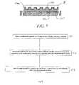
- FIG. 6is a simplified elevation view of imprint material disposed on a substrate in accordance with the present invention.
- FIG. 7is a simplified elevation view of imprint material disposed on a substrate in accordance with an alternate embodiment
- FIG. 8is a simplified-elevation view of imprint material, shown in FIG. 6 , after contact with the mold.
- FIG. 9is a flow diagram showing pattern priming in accordance with an alternate embodiment of the present invention.
- FIG. 1depicts a lithographic system 10 in accordance with one embodiment of the present invention that includes a pair of spaced-apart bridge supports 12 having a bridge 14 and a stage support 16 extending therebetween. Bridge 14 and stage support 16 are spaced-apart. Coupled to bridge 14 is an imprint head 18 , which extends from bridge 14 toward stage support 16 . Disposed upon stage support 16 to face imprint head 18 is a motion stage 20 . Motion stage 20 is configured to move with respect to stage support 16 along X and Y axes. A radiation source 22 is coupled to system 10 to impinge actinic radiation upon motion stage 20 . As shown, radiation source 22 is coupled to bridge 14 and includes a power generator 23 connected to radiation source 22 .
- Mold 28includes a plurality of features defined by a plurality of spaced-apart recessions 28 a and protrusions 28 b .
- the plurality of featuresdefines an original pattern that is to be transferred into a substrate 31 positioned on motion stage 20 .
- Substrate 31may comprise of a bare wafer or a wafer with one or more layers disposed thereon.
- imprint head 18is adapted to move along the Z axis and vary a distance “d” between mold 28 and substrate 31 . In this manner, the features on mold 28 may be imprinted into a conformable region of substrate 31 , discussed more fully below.
- Radiation source 22is located so that mold 28 is positioned between radiation source 22 and substrate 31 .
- mold 28is fabricated from material that allows it to be substantially transparent to the radiation produced by radiation source 22 .
- a conformable regionsuch as an imprinting layer 34 , is disposed on a portion of surface 32 that presents a substantially planar profile.
- the conformable regionmay be formed using any known technique to produce conformable material on such as a hot embossing process disclosed in U.S. Pat. No. 5,772,905 to Chou, which is incorporated by reference in its entirety herein, or a laser assisted direct imprinting (LADI) process of the type described by Chou et al. in Ultrafast and Direct Imprint of Nanostructures in Silicon , Nature, Col. 417, pp. 835–837, June 2002.
- LADIlaser assisted direct imprinting
- conformable regionconsists of imprinting layer 34 being deposited as a plurality of spaced-apart discrete droplets 36 of material 36 a on substrate 31 , discussed more fully below.
- Imprinting layer 34is formed from a material 36 a that may be selectively polymerized and cross-linked to record the original pattern therein, defining a recorded pattern.
- Material 36 ais shown in FIG. 4 as being cross-linked at points 36 b , forming cross-linked polymer material 36 c.
- the pattern recorded in imprinting layer 34is produced, in part, by mechanical contact with mold 28 .
- imprint head 18reduces the distance “d” to allow imprinting layer 34 to come into mechanical contact with mold 28 , spreading droplets 36 so as to form imprinting layer 34 with a contiguous formation of material 36 a over surface 32 .
- distance “d”is reduced to allow sub-portions 34 a of imprinting layer 34 to ingress into and fill recessions 28 a.
- material 36 ais provided with the requisite properties to completely fill recessions 28 a while covering surface 32 with a contiguous formation of material 36 a .
- sub-portions 34 b of imprinting layer 34 in superimposition with protrusions 28 bremain after the desired, usually minimum distance “d”, has been reached, leaving sub-portions 34 a with a thickness t 1 , and sub-portions 34 b with a thickness, t 2 .
- Thicknesses “t 1 ” and “t 2 ”may be any thickness desired, dependent upon the application.
- t 1is selected so as to be no greater than twice the width u of sub-portions 34 a , i.e., t 1 23 2u, shown more clearly in FIG. 5 .
- radiation source 22produces actinic radiation that polymerizes and cross-links material 36 a , forming polymer material 36 c in which a substantial portion thereof is cross-linked.
- material 36 atransforms to material 36 c , which is a solid, forming imprinting layer 134 , shown in FIG. 5 .
- material 36 cis solidified to provide side 34 c of imprinting layer 134 with a shape conforming to a shape of a surface 28 c of mold 28 , with imprinting layer 134 having recesses 30 .
- imprint head 18shown in FIG. 2 , is moved to increase distance “d” so that mold 28 and imprinting layer 134 are spaced-apart.
- substrate 31 and imprinting layer 134may be etched to transfer the pattern of imprinting layer 134 into substrate 31 , providing a patterned surface (not shown).
- the material from which imprinting layer 134 is formedmay be varied to define a relative etch rate with respect to substrate 31 , as desired.
- imprinting layer 134may be provided with an etch differential with respect to photo-resist material (not shown) selectively disposed thereon.
- the photo-resist material (not shown)may be provided to further pattern imprinting layer 134 , using known techniques. Any etch process may be employed, dependent upon the etch rate desired and the underlying constituents that form substrate 31 and imprinting layer 134 . Exemplary etch processes may include plasma etching, reactive ion etching, chemical wet etching and the like.
- an exemplary radiation source 22may produce ultraviolet radiation; however, any known radiation source may be employed.
- the selection of radiation employed to initiate the polymerization of the material in imprinting layer 34is known to one skilled in the art and typically depends on the specific application which is desired.
- the plurality of features on mold 28are shown as recessions 28 a extending along a direction parallel to protrusions 28 b that provide a cross-section of mold 28 with a shape of a battlement.
- recessions 28 a and protrusions 28 bmay correspond to virtually any feature required to create an integrated circuit and may be as small as a few tenths of nanometers.
- the pattern produced by the present patterning techniquemay be transferred into substrate 31 to provide features having aspect ratios as great as 30:1.
- one embodiment of mold 28has recessions 28 a defining an aspect ratio in a range of 1:1 to 10:1.
- protrusions 28 bhave a width W 1 in a range of about 10 nm to about 5000 ⁇ m
- recessions 28 ahave a width W 2 in a range of 10 nm to about 5000 ⁇ m.
- mold 28 and/or template 26may be formed from various conventional materials, such as, but not limited to, fused-silica, quartz, silicon, organic polymers, siloxane polymers, borosilicate glass, fluorocarbon polymers, metal, hardened sapphire and the like.
- the characteristics of material 36 aare important to efficiently pattern substrate 31 in light of the unique deposition process employed.
- material 36 ais deposited on substrate 31 as a plurality of discrete and spaced-apart droplets 36 .
- the combined volume of droplets 36is such that the material 36 a is distributed appropriately over an area of surface 32 where imprinting layer 34 is to be formed.
- imprinting layer 34is spread and patterned concurrently, with the pattern being subsequently set into imprinting layer 34 by exposure to radiation, such as ultraviolet radiation.
- material 36 ahave certain characteristics to facilitate rapid and even spreading of material 36 a in droplets 36 over surface 32 so that all thicknesses t 1 are substantially uniform and all thicknesses t 2 are substantially uniform.
- the desirable characteristicsinclude having a low viscosity, e.g., in a range of 0.5 to 5 centepoise (csp), as well as the ability to wet surface of substrate 31 and/or mold 28 and to avoid subsequent pit or hole formation after polymerization. With these characteristics satisfied, imprinting layer 34 may be made sufficiently thin while avoiding formation of pits or holes in the thinner regions, such as sub-portions 34 b , shown in FIG. 5 .
- substrate 31may be formed from a number of different materials.
- the chemical composition of surface 32varies dependent upon the material from which substrate 31 is formed.
- substrate 31may be formed from silicon, plastics, gallium arsenide, mercury telluride, and composites thereof.
- substrate 31may include one or more layers in sub-portion 34 b , e.g., dielectric layer, metal layer, semiconductor layer, planarization layer and the like.
- an exemplary composition for material 36 ais as follows:
- isobornyl acrylatecomprises approximately 55% of the composition, n-hexyl acrylate comprised approximately 27%, ethylene glycol diacrylate comprises approximately 15% and the initiator 2-hydroxy-2-methyl-1-phenyl-propan-1-one comprised approximately 3%.
- the initiatoris sold under the trade name DAROCUR® 1173 by CIBA® of Tarrytown, N.Y.
- the above-identified compositionalso includes stabilizers that are well known in the chemical art to increase the operational life of the composition.
- COMPOSITION 1is typically employed with a template treated to have a mold surface that is hydrophobic and/or low surface energy, i.e. an a priori release layer.
- the composition from which material 36 a is formedmay include an additive that reduces the surface tension of COMPOSITION 1.
- material 36 amay include, as an additive, a surfactant.
- a surfactantis defined as any molecule, one tail of which is hydrophobic.
- Surfactantsmay be either fluorine containing, e.g., include a fluorine chain, or may not include any fluorine in the surfactant molecule structure.
- Thisprovides material 36 a with the following composition:
- the ZONYL® FSO-100 additivecomprises less than 1% of the composition, with the relative amounts of the remaining components being as discussed above with respect to COMPOSITION 1. However, the percentage of ZONYL® FSO-100 may be greater than 1%.
- COMPOSITION 2abrogates the need for an a priori release layer, i.e., a separate hydrophobic and/or low surface energy release layer disposed on mold 28 .
- COMPOSITION 2provides desirable release properties to mold 28 and imprinting layer 34 so that material 36 c , shown in FIG. 4 , does not adhere to mold 28 with sufficient force to distort the pattern recorded therein. It is believed that the ZONYL® FSO-100 becomes concentrated in a first region of material 36 a , shown in FIG. 3 . The polymerizable compound becomes concentrated in a second region of material 36 a.
- droplets 36would have a higher concentration of the ZONYL® FSO-100 additive in region 136 , compared with region 137 , in which the polymerizable compound is concentrated.
- the additivewould be concentrated in a region 236 , and the polymerizable compound being concentrated in region 237 , shown in FIG. 7 .
- material 36 aupon contact with material 36 a and exposure to actinic radiation, material 36 a is transformed to material 36 c and a first interface 136 a is defined between region 136 and mold 28 .
- a second interface 137 ais formed between regions 136 and 137 . It is believed that some portion of material 36 c associated with region 136 , if not all, has an affinity for the mold 28 that is greater than the attraction between that portion and the material 36 c associated with region 137 .
- a sub-section, or all of sub-portions 34 a and 34 bshown in FIG. 5 , separates from region 137 , thereby minimizing damage to the pattern recorded in material 36 c due to adhesion forces between mold 28 and material 36 c.
- interface 136 adefines a first interfacial energy step associated therewith
- second interface 137 adefines a second interfacial energy step, with the first interfacial energy step being greater than the second interfacial energy step.
- the first interfacial energy stepis defined by the difference in surface energy of mold 28 and surface tension of material 36 c in region 136 .
- the second interfacial surface energyis defined by the adhesion of material 36 c associated with region 136 for material 36 c associated with region 137 .
- the interfacial surface energy step at interface 136 ais sufficiently large to overcome the interfacial energy step at interface 137 .
- an additional advantage provided by COMPOSITION 2is that the time required to wet mold 28 and, therefore, spread droplets 36 may be reduced.
- the surface of mold 28may be provided with a high surface energy, e.g., 60 to 250 milli-Newtons/meter.
- the wettability of the surface of mold 28 for COMPOSITION 2, as defined by the contact angle method,may be in a range of 10 degrees or less. This minimizes the time required to fill the features of the pattern on mold 28 .
- the ZONYL® FSO-100 additiveprovides COMPOSITION 2 with a wettability, as defined by the contact angle method, in a range of 75 to 90 degrees, thereby augmenting the wettability of mold 28 , thereby further reducing the time required to spread droplets 36 .
- COMPOSITION 2may be employed with an a priori release layer, such as those known in the prior art, to further improve release properties.
- Another manner by which to improve the release properties of mold 28includes conditioning the pattern of mold 28 by exposing the same to a conditioning mixture including an additive that will remain on mold 28 to reduce the surface energy of the mold surface.
- An exemplary additiveis a surfactant.
- mold 28was exposed to a mixture that included approximately 0.1% or more of ZONYL® FSO-100 with the remainder comprising isopropyl alcohol (IPA).
- Exposure of the patternmay be achieved by virtually any manner known in the art, including dipping the pattern into a volume of the conditioning mixture, wiping the pattern with a cloth saturated with the conditioning mixture and spraying a stream of the conditioning mixture onto the surface.
- the IPA in the conditioning mixtureis then allowed to evaporate before using the mold 28 . In this manner, the IPA facilitates removing, from the pattern, undesired contaminants while leaving the additive, thereby conditioning the surface of the pattern.
- the conditioning mixturemay be employed with COMPOSITION 2 to augment improvement of the release properties provided by COMPOSITION 2.
- the additive in the conditioning mixturemay be the same or differ from the additive in COMPOSITION 2.
- the conditioning mixturemay be employed with COMPOSITION 1, or any other polymerizable material suitable for imprint lithography, as well as other imprint processes such as the hot embossing and laser assisted imprint processes.
- Pattern primingis achieved by selectively contacting the conformable region with the pattern a sufficient number of times to accurately reproduce, in the conformable region, a pattern complementary to the initial pattern. Specifically, it was found that by repeatably contacting imprint material 36 a , shown in FIG. 3 , the complementary pattern formed improves with each successive imprint. After a sufficient number of imprints, an accurate complementary reproduction of the pattern in mold 28 is formed.
- the pattern priming techniquemay be employed in combination with the aforementioned conditioning mixture and either COMPOSITION 1 or COMPOSITION 2 and, or with COMPOSITION 2, alone, i.e., COMPOSITION 2 without use of the conditioning mixture.
- the number of imprints required to be produced before an accurate complementary reproduction of the pattern occursis inversely proportional to the quantity of additive in COMPOSITION 2. Specifically, it is believed that by increasing the quantity of the additive in COMPOSITION 2 that the number of imprints required before an accurate complementary reproduction of the pattern occurs is reduced. This results from a transfer of the surfactant molecules onto the mold surface upon contact by the mold with COMPOSITION 2 resulting from the surfactant being attracted thereto by formation of hydrogen bonds with the mold.
- imprint primingwould include forming a conformable material on a first substrate, defining a priming substrate at step 300 .
- mold 28contacts the conformable region a sufficient number of times to accurately reproduce, in the conformable material on the priming substrate, the pattern on mold 28 .
- mold 28is placed in contact with a first sub-portion of the conformable material. Thereafter, the first sub-portion is polymerized and mold 28 is spaced-part therefrom. Mold 28 is then placed in contact with a second sub-portion of the conformable material, which is spaced-apart from the first sub-portion.
- the conformable material associated with the second sub-portionis polymerized and the process is repeated until an accurate pattern is recorded in the conformable material that is complementary to the pattern on mold 28 .
- a primed moldis generated.
- the primed moldis placed in contact with conformable material on a second substrate, referred to as a process substrate.
- the patternmay be recorded therein by polymerizing the conformable material using well known imprint lithography techniques. In this manner, the primed mold may be employed to complete the patterning of the process substrate.
Landscapes
- Engineering & Computer Science (AREA)
- Nanotechnology (AREA)
- Chemical & Material Sciences (AREA)
- Physics & Mathematics (AREA)
- Crystallography & Structural Chemistry (AREA)
- General Physics & Mathematics (AREA)
- Mathematical Physics (AREA)
- Theoretical Computer Science (AREA)
- Condensed Matter Physics & Semiconductors (AREA)
- Manufacturing & Machinery (AREA)
- Shaping Of Tube Ends By Bending Or Straightening (AREA)
- Exposure Of Semiconductors, Excluding Electron Or Ion Beam Exposure (AREA)
- Moulds For Moulding Plastics Or The Like (AREA)
Abstract
Description
Claims (14)
Priority Applications (10)
| Application Number | Priority Date | Filing Date | Title |
|---|---|---|---|
| US10/463,396US7157036B2 (en) | 2003-06-17 | 2003-06-17 | Method to reduce adhesion between a conformable region and a pattern of a mold |
| CNB200480016523XACN100572032C (en) | 2003-06-17 | 2004-06-10 | Method for reducing adhesion between bonding area and mold pattern |
| EP04776543.3AEP1633545B1 (en) | 2003-06-17 | 2004-06-10 | Method to reduce adhesion between a conformable region and a pattern of a mold |
| KR1020057024135AKR101202653B1 (en) | 2003-06-17 | 2004-06-10 | Method to reduce adhesion between a conformable region and a pattern of a mold |
| PCT/US2004/018857WO2005000552A2 (en) | 2003-06-17 | 2004-06-10 | Method to reduce adhesion between a conformable region and a pattern of a mold |
| JP2006517254AJP4791357B2 (en) | 2003-06-17 | 2004-06-10 | Method for reducing adhesion between a molded area and a mold pattern |
| MYPI20042293AMY136832A (en) | 2003-06-17 | 2004-06-15 | Method to reduce adhesion between a conformable region and a pattern of a mold |
| TW093117326ATWI358608B (en) | 2003-06-17 | 2004-06-16 | Method to reduce adhesion between a conformable re |
| US11/459,797US20060279024A1 (en) | 2003-06-17 | 2006-07-25 | Method for providing desirable wetting and release characteristics between a mold and a polymerizable composition |
| US12/404,024US8152511B2 (en) | 2003-06-17 | 2009-03-13 | Composition to reduce adhesion between a conformable region and a mold |
Applications Claiming Priority (1)
| Application Number | Priority Date | Filing Date | Title |
|---|---|---|---|
| US10/463,396US7157036B2 (en) | 2003-06-17 | 2003-06-17 | Method to reduce adhesion between a conformable region and a pattern of a mold |
Related Child Applications (1)
| Application Number | Title | Priority Date | Filing Date |
|---|---|---|---|
| US11/459,797ContinuationUS20060279024A1 (en) | 2003-06-17 | 2006-07-25 | Method for providing desirable wetting and release characteristics between a mold and a polymerizable composition |
Publications (2)
| Publication Number | Publication Date |
|---|---|
| US20040256764A1 US20040256764A1 (en) | 2004-12-23 |
| US7157036B2true US7157036B2 (en) | 2007-01-02 |
Family
ID=33517095
Family Applications (2)
| Application Number | Title | Priority Date | Filing Date |
|---|---|---|---|
| US10/463,396Expired - LifetimeUS7157036B2 (en) | 2003-06-17 | 2003-06-17 | Method to reduce adhesion between a conformable region and a pattern of a mold |
| US11/459,797AbandonedUS20060279024A1 (en) | 2003-06-17 | 2006-07-25 | Method for providing desirable wetting and release characteristics between a mold and a polymerizable composition |
Family Applications After (1)
| Application Number | Title | Priority Date | Filing Date |
|---|---|---|---|
| US11/459,797AbandonedUS20060279024A1 (en) | 2003-06-17 | 2006-07-25 | Method for providing desirable wetting and release characteristics between a mold and a polymerizable composition |
Country Status (8)
| Country | Link |
|---|---|
| US (2) | US7157036B2 (en) |
| EP (1) | EP1633545B1 (en) |
| JP (1) | JP4791357B2 (en) |
| KR (1) | KR101202653B1 (en) |
| CN (1) | CN100572032C (en) |
| MY (1) | MY136832A (en) |
| TW (1) | TWI358608B (en) |
| WO (1) | WO2005000552A2 (en) |
Cited By (169)
| Publication number | Priority date | Publication date | Assignee | Title |
|---|---|---|---|---|
| US20040116548A1 (en)* | 2002-12-12 | 2004-06-17 | Molecular Imprints, Inc. | Compositions for dark-field polymerization and method of using the same for imprint lithography processes |
| US20050270312A1 (en)* | 2004-06-03 | 2005-12-08 | Molecular Imprints, Inc. | Fluid dispensing and drop-on-demand dispensing for nano-scale manufacturing |
| US20060035029A1 (en)* | 2004-08-16 | 2006-02-16 | Molecular Imprints, Inc. | Method to provide a layer with uniform etch characteristics |
| US20060175736A1 (en)* | 2004-01-23 | 2006-08-10 | Molecular Imprints, Inc. | Method of providing desirable wetting and release characterstics between a mold and a polymerizable composition |
| US20070021520A1 (en)* | 2005-07-22 | 2007-01-25 | Molecular Imprints, Inc. | Composition for adhering materials together |
| US20070017631A1 (en)* | 2005-07-22 | 2007-01-25 | Molecular Imprints, Inc. | Method for adhering materials together |
| US20070132152A1 (en)* | 2005-12-08 | 2007-06-14 | Molecular Imprints, Inc. | Method and System for Double-Sided Patterning of Substrates |
| US20070141271A1 (en)* | 2004-09-23 | 2007-06-21 | Molecular Imprints, Inc. | Method for controlling distribution of fluid components on a body |
| US20070138699A1 (en)* | 2005-12-21 | 2007-06-21 | Asml Netherlands B.V. | Imprint lithography |
| US20070212494A1 (en)* | 2005-07-22 | 2007-09-13 | Molecular Imprints, Inc. | Method for Imprint Lithography Utilizing an Adhesion Primer Layer |
| US20070272825A1 (en)* | 2004-01-23 | 2007-11-29 | Molecular Imprints, Inc. | Composition to Reduce Adhesion Between a Conformable Region and a Mold |
| US20080000871A1 (en)* | 2005-08-29 | 2008-01-03 | Kahp-Yang Suh | Method for forming nanostructure having high aspect ratio and method for forming nanopattern using the same |
| US20080021587A1 (en)* | 2006-07-24 | 2008-01-24 | Wei Wu | Compensation for distortion in contact lithography |
| US20080110557A1 (en)* | 2006-11-15 | 2008-05-15 | Molecular Imprints, Inc. | Methods and Compositions for Providing Preferential Adhesion and Release of Adjacent Surfaces |
| US20080141862A1 (en)* | 2003-10-02 | 2008-06-19 | Molecular Imprints, Inc. | Single Phase Fluid Imprint Lithography Method |
| US20080199816A1 (en)* | 2000-07-17 | 2008-08-21 | The University Of Texas Board Of Regents | Method of Automatic Fluid Dispensing for Imprint Lithography Processes |
| US20080254626A1 (en)* | 2004-03-29 | 2008-10-16 | Canon Kabushiki Kaisha | Processing apparatus |
| US20080308971A1 (en)* | 2007-06-18 | 2008-12-18 | Molecular Imprints, Inc. | Solvent-Assisted Layer Formation for Imprint Lithography |
| US20090037004A1 (en)* | 2000-10-12 | 2009-02-05 | Molecular Imprints, Inc. | Method and System to Control Movement of a Body for Nano-Scale Manufacturing |
| US20090140458A1 (en)* | 2007-11-21 | 2009-06-04 | Molecular Imprints, Inc. | Porous template and imprinting stack for nano-imprint lithography |
| US20090155583A1 (en)* | 2005-07-22 | 2009-06-18 | Molecular Imprints, Inc. | Ultra-thin Polymeric Adhesion Layer |
| US7670530B2 (en) | 2006-01-20 | 2010-03-02 | Molecular Imprints, Inc. | Patterning substrates employing multiple chucks |
| US20100072671A1 (en)* | 2008-09-25 | 2010-03-25 | Molecular Imprints, Inc. | Nano-imprint lithography template fabrication and treatment |
| US20100084376A1 (en)* | 2008-10-02 | 2010-04-08 | Molecular Imprints, Inc. | Nano-imprint lithography templates |
| US20100090341A1 (en)* | 2008-10-14 | 2010-04-15 | Molecular Imprints, Inc. | Nano-patterned active layers formed by nano-imprint lithography |
| US20100095862A1 (en)* | 2008-10-22 | 2010-04-22 | Molecular Imprints, Inc. | Double Sidewall Angle Nano-Imprint Template |
| US20100098940A1 (en)* | 2008-10-20 | 2010-04-22 | Molecular Imprints, Inc. | Nano-Imprint Lithography Stack with Enhanced Adhesion Between Silicon-Containing and Non-Silicon Containing Layers |
| US20100096776A1 (en)* | 2008-10-21 | 2010-04-22 | Molecular Imprints, Inc. | Reduction of Stress During Template Separation |
| US20100104852A1 (en)* | 2008-10-23 | 2010-04-29 | Molecular Imprints, Inc. | Fabrication of High-Throughput Nano-Imprint Lithography Templates |
| US20100102469A1 (en)* | 2008-10-24 | 2010-04-29 | Molecular Imprints, Inc. | Strain and Kinetics Control During Separation Phase of Imprint Process |
| US20100112236A1 (en)* | 2008-10-30 | 2010-05-06 | Molecular Imprints, Inc. | Facilitating Adhesion Between Substrate and Patterned Layer |
| US20100109205A1 (en)* | 2008-11-04 | 2010-05-06 | Molecular Imprints, Inc. | Photocatalytic reactions in nano-imprint lithography processes |
| US20100112220A1 (en)* | 2008-11-03 | 2010-05-06 | Molecular Imprints, Inc. | Dispense system set-up and characterization |
| US20100110409A1 (en)* | 2008-10-30 | 2010-05-06 | Molecular Imprints, Inc. | Separation in an Imprint Lithography Process |
| US20100109195A1 (en)* | 2008-11-05 | 2010-05-06 | Molecular Imprints, Inc. | Release agent partition control in imprint lithography |
| US20100237042A1 (en)* | 2009-03-23 | 2010-09-23 | Intevac, Inc. | Process for optimization of island to trench ratio in patterned media |
| US7811505B2 (en) | 2004-12-07 | 2010-10-12 | Molecular Imprints, Inc. | Method for fast filling of templates for imprint lithography using on template dispense |
| US20100286811A1 (en)* | 2004-06-15 | 2010-11-11 | Molecular Imprints, Inc. | Residual Layer Thickness Measurement and Correction |
| WO2010147671A1 (en) | 2009-06-19 | 2010-12-23 | Molecular Imprints, Inc. | Dual zone template chuck |
| WO2011002518A2 (en) | 2009-07-02 | 2011-01-06 | Molecular Imprints, Inc. | Chucking system with recessed support feature |
| WO2011016839A1 (en) | 2009-08-04 | 2011-02-10 | Board Of Regents, The University Of Texas System | Nanostructured organic solar cells |
| US20110031650A1 (en)* | 2009-08-04 | 2011-02-10 | Molecular Imprints, Inc. | Adjacent Field Alignment |
| US20110048518A1 (en)* | 2009-08-26 | 2011-03-03 | Molecular Imprints, Inc. | Nanostructured thin film inorganic solar cells |
| US20110049096A1 (en)* | 2009-08-26 | 2011-03-03 | Board Of Regents, The University Of Texas System | Functional Nanoparticles |
| US20110084417A1 (en)* | 2009-10-08 | 2011-04-14 | Molecular Imprints, Inc. | Large area linear array nanoimprinting |
| US20110105366A1 (en)* | 2007-06-18 | 2011-05-05 | Illumina, Inc. | Microfabrication methods for the optimal patterning of substrates |
| WO2011066450A2 (en) | 2009-11-24 | 2011-06-03 | Molecular Imprints, Inc. | Adhesion layers in nanoimprint lithography |
| US20110140306A1 (en)* | 2004-02-27 | 2011-06-16 | Molecular Imprints, Inc. | Composition for an Etching Mask Comprising a Silicon-Containing Material |
| WO2011072202A1 (en) | 2009-12-10 | 2011-06-16 | Molecular Imprints, Inc. | Imprint lithography template |
| US20110183027A1 (en)* | 2010-01-26 | 2011-07-28 | Molecular Imprints, Inc. | Micro-Conformal Templates for Nanoimprint Lithography |
| US20110183521A1 (en)* | 2010-01-27 | 2011-07-28 | Molecular Imprints, Inc. | Methods and systems of material removal and pattern transfer |
| US20110183070A1 (en)* | 2010-01-28 | 2011-07-28 | Molecular Imprints, Inc. | Roll-to-roll imprint lithography and purging system |
| US20110189329A1 (en)* | 2010-01-29 | 2011-08-04 | Molecular Imprints, Inc. | Ultra-Compliant Nanoimprint Lithography Template |
| WO2011094672A2 (en) | 2010-01-29 | 2011-08-04 | Molecular Imprints, Inc. | Nanoimprint lithography processes for forming nanoparticles |
| WO2011094015A1 (en) | 2010-01-28 | 2011-08-04 | Molecular Imprints, Inc. | Solar cell fabrication by nanoimprint lithography |
| WO2011097514A2 (en) | 2010-02-05 | 2011-08-11 | Molecular Imprints, Inc. | Templates having high contrast alignment marks |
| US20110193251A1 (en)* | 2010-02-09 | 2011-08-11 | Molecular Imprints, Inc. | Process Gas Confinement for Nano-Imprinting |
| US20110215503A1 (en)* | 2004-11-24 | 2011-09-08 | Molecular Imprints, Inc. | Reducing Adhesion between a Conformable Region and a Mold |
| WO2011139782A1 (en) | 2010-04-27 | 2011-11-10 | Molecular Imprints, Inc. | Separation control substrate/template for nanoimprint lithography |
| WO2012006521A1 (en) | 2010-07-08 | 2012-01-12 | Molecular Imprints, Inc. | Enhanced densification of silicon oxide layers |
| US8142703B2 (en) | 2005-10-05 | 2012-03-27 | Molecular Imprints, Inc. | Imprint lithography method |
| US20130059090A1 (en)* | 2011-09-01 | 2013-03-07 | Daisuke Kawamura | Resist material for imprinting, pattern formation method, and imprinting apparatus |
| WO2013126750A1 (en) | 2012-02-22 | 2013-08-29 | Molecular Imprints, Inc. | Large area imprint lithography |
| US20140242744A1 (en)* | 2011-09-26 | 2014-08-28 | Solarity, Inc. | Substrate and superstrate design and process for nano-imprinting lithography of light and carrier collection management devices |
| US8828297B2 (en) | 2010-11-05 | 2014-09-09 | Molecular Imprints, Inc. | Patterning of non-convex shaped nanostructures |
| WO2014145634A2 (en) | 2013-03-15 | 2014-09-18 | Canon Nanotechnologies, Inc. | Nano imprinting with reusable polymer template with metallic or oxide coating |
| US8889332B2 (en) | 2004-10-18 | 2014-11-18 | Canon Nanotechnologies, Inc. | Low-K dielectric functional imprinting materials |
| US8891080B2 (en) | 2010-07-08 | 2014-11-18 | Canon Nanotechnologies, Inc. | Contaminate detection and substrate cleaning |
| US8916200B2 (en) | 2010-11-05 | 2014-12-23 | Molecular Imprints, Inc. | Nanoimprint lithography formation of functional nanoparticles using dual release layers |
| US8926888B2 (en) | 2011-02-25 | 2015-01-06 | Board Of Regents, The University Of Texas System | Fluorinated silazane release agents in nanoimprint lithography |
| US8935981B2 (en) | 2010-09-24 | 2015-01-20 | Canon Nanotechnologies, Inc. | High contrast alignment marks through multiple stage imprinting |
| US8967992B2 (en) | 2011-04-25 | 2015-03-03 | Canon Nanotechnologies, Inc. | Optically absorptive material for alignment marks |
| WO2015070054A1 (en) | 2013-11-08 | 2015-05-14 | Canon Nanotechnologies, Inc. | Low contact imprint lithography template chuck system for improved overlay correction |
| WO2015089158A1 (en) | 2013-12-10 | 2015-06-18 | Canon Nanotechnologies, Inc. | Imprint lithography template and method for zero-gap imprinting |
| US9070803B2 (en) | 2010-05-11 | 2015-06-30 | Molecular Imprints, Inc. | Nanostructured solar cell |
| WO2015103232A1 (en) | 2013-12-30 | 2015-07-09 | Canon Nanotechnologies, Inc. | Methods for uniform imprint pattern transfer of sub-20 nm features |
| US9193199B2 (en) | 2013-11-20 | 2015-11-24 | Eastman Kodak Company | PDMS imprinting stamp with embedded flexure |
| US9452574B2 (en) | 2011-12-19 | 2016-09-27 | Canon Nanotechnologies, Inc. | Fabrication of seamless large area master templates for imprint lithography using step and repeat tools |
| US9513543B2 (en) | 2013-11-20 | 2016-12-06 | Eastman Kodak Company | Method for forming a non-deformable patterned template |
| EP3141956A1 (en) | 2015-09-08 | 2017-03-15 | Canon Kabushiki Kaisha | Substrate pretreatment for reducing fill time in nanoimprint lithography |
| US9634163B2 (en) | 2002-06-08 | 2017-04-25 | Lccm Solar, Llc | Lateral collection photovoltaics |
| US9651862B2 (en) | 2013-07-12 | 2017-05-16 | Canon Nanotechnologies, Inc. | Drop pattern generation for imprint lithography with directionally-patterned templates |
| US9971249B1 (en) | 2017-02-27 | 2018-05-15 | Canon Kabushiki Kaisha | Method and system for controlled ultraviolet light exposure |
| KR20180071971A (en)* | 2016-12-20 | 2018-06-28 | 캐논 가부시끼가이샤 | Methods for controlling extrusions during imprint template replication processes |
| US10035296B2 (en) | 2016-10-13 | 2018-07-31 | Canon Kabushiki Kaisha | Methods for controlling spread of imprint material |
| US20180231418A1 (en)* | 2014-09-26 | 2018-08-16 | Korea Institute Of Machinery & Materials | Substrate On Which Multiple Nanogaps Are Formed, And Manufacturing Method Therefor |
| US10079152B1 (en) | 2017-02-24 | 2018-09-18 | Canon Kabushiki Kaisha | Method for forming planarized etch mask structures over existing topography |
| US10095106B2 (en) | 2016-03-31 | 2018-10-09 | Canon Kabushiki Kaisha | Removing substrate pretreatment compositions in nanoimprint lithography |
| US10131134B2 (en) | 2015-10-30 | 2018-11-20 | Canon Kabushiki Kaisha | System and method for discharging electrostatic charge in nanoimprint lithography processes |
| US10134588B2 (en) | 2016-03-31 | 2018-11-20 | Canon Kabushiki Kaisha | Imprint resist and substrate pretreatment for reducing fill time in nanoimprint lithography |
| US10208183B2 (en) | 2013-08-30 | 2019-02-19 | Canon Kabushiki Kaisha | Curable composition, film, and method of producing film |
| US10211051B2 (en) | 2015-11-13 | 2019-02-19 | Canon Kabushiki Kaisha | Method of reverse tone patterning |
| US10303049B2 (en) | 2017-03-22 | 2019-05-28 | Canon Kabushiki Kaisha | Reducing electric charge in imprint lithography |
| US10317793B2 (en) | 2017-03-03 | 2019-06-11 | Canon Kabushiki Kaisha | Substrate pretreatment compositions for nanoimprint lithography |
| US10409178B2 (en) | 2017-12-18 | 2019-09-10 | Canon Kabushiki Kaisha | Alignment control in nanoimprint lithography based on real-time system identification |
| US10488753B2 (en) | 2015-09-08 | 2019-11-26 | Canon Kabushiki Kaisha | Substrate pretreatment and etch uniformity in nanoimprint lithography |
| US10509313B2 (en) | 2016-06-28 | 2019-12-17 | Canon Kabushiki Kaisha | Imprint resist with fluorinated photoinitiator and substrate pretreatment for reducing fill time in nanoimprint lithography |
| US10514599B2 (en) | 2014-08-14 | 2019-12-24 | Canon Kabushiki Kaisha | Imprint apparatus and method of manufacturing article |
| US10534259B2 (en) | 2017-03-28 | 2020-01-14 | Canon Kabushiki Kaisha | Method and system for imprint force control |
| US10578984B2 (en) | 2016-12-20 | 2020-03-03 | Canon Kabushiki Kaisha | Adaptive chucking system |
| US10578965B2 (en) | 2016-03-31 | 2020-03-03 | Canon Kabushiki Kaisha | Pattern forming method |
| US10578964B2 (en) | 2013-12-31 | 2020-03-03 | Canon Nanotechnologies, Inc. | Asymmetric template shape modulation for partial field imprinting |
| US10580659B2 (en) | 2017-09-14 | 2020-03-03 | Canon Kabushiki Kaisha | Planarization process and apparatus |
| US20200073228A1 (en)* | 2018-08-30 | 2020-03-05 | Toshiba Memory Corporation | Original plate |
| US10620539B2 (en) | 2016-03-31 | 2020-04-14 | Canon Kabushiki Kaisha | Curing substrate pretreatment compositions in nanoimprint lithography |
| US10627715B2 (en) | 2016-10-31 | 2020-04-21 | Canon Kabushiki Kaisha | Method for separating a nanoimprint template from a substrate |
| US10654216B2 (en) | 2016-03-30 | 2020-05-19 | Canon Kabushiki Kaisha | System and methods for nanoimprint lithography |
| US10663869B2 (en) | 2017-12-11 | 2020-05-26 | Canon Kabushiki Kaisha | Imprint system and imprinting process with spatially non-uniform illumination |
| US10712660B2 (en) | 2016-12-21 | 2020-07-14 | Canon Kabushiki Kaisha | Template for imprint lithography including a recession and an apparatus and method of using the template |
| US10739675B2 (en) | 2018-05-31 | 2020-08-11 | Canon Kabushiki Kaisha | Systems and methods for detection of and compensation for malfunctioning droplet dispensing nozzles |
| US10754245B2 (en) | 2016-03-31 | 2020-08-25 | Canon Kabushiki Kaisha | Pattern forming method as well as production methods for processed substrate, optical component, circuit board, electronic component and imprint mold |
| US10754244B2 (en) | 2016-03-31 | 2020-08-25 | Canon Kabushiki Kaisha | Pattern forming method as well as production methods for processed substrate, optical component, circuit board, electronic component and imprint mold |
| US10754078B2 (en) | 2018-12-20 | 2020-08-25 | Canon Kabushiki Kaisha | Light source, a shaping system using the light source and an article manufacturing method |
| US10754243B2 (en) | 2016-03-31 | 2020-08-25 | Canon Kabushiki Kaisha | Pattern forming method as well as production methods for processed substrate, optical component, circuit board, electronic component and imprint mold |
| US10788749B2 (en) | 2017-11-30 | 2020-09-29 | Canon Kabushiki Kaisha | System and method for improving the throughput of a nanoimprint system |
| US10829644B2 (en) | 2016-03-31 | 2020-11-10 | Canon Kabushiki Kaisha | Pattern forming method as well as production methods for processed substrate, optical component, circuit board, electronic component and imprint mold |
| US10845700B2 (en) | 2016-03-31 | 2020-11-24 | Canon Kabushiki Kaisha | Pattern forming method as well as production methods for processed substrate, optical component, circuit board, electronic component and imprint mold |
| US10866510B2 (en) | 2017-07-31 | 2020-12-15 | Canon Kabushiki Kaisha | Overlay improvement in nanoimprint lithography |
| US10883006B2 (en) | 2016-03-31 | 2021-01-05 | Canon Kabushiki Kaisha | Pattern forming method as well as production methods for processed substrate, optical component, circuit board, electronic component and imprint mold |
| US10895806B2 (en) | 2017-09-29 | 2021-01-19 | Canon Kabushiki Kaisha | Imprinting method and apparatus |
| US10921706B2 (en) | 2018-06-07 | 2021-02-16 | Canon Kabushiki Kaisha | Systems and methods for modifying mesa sidewalls |
| US10935883B2 (en) | 2017-09-29 | 2021-03-02 | Canon Kabushiki Kaisha | Nanoimprint template with light blocking material and method of fabrication |
| US10935884B2 (en) | 2017-03-08 | 2021-03-02 | Canon Kabushiki Kaisha | Pattern forming method and methods for manufacturing processed substrate, optical component and quartz mold replica as well as coating material for imprint pretreatment and set thereof with imprint resist |
| US10969680B2 (en) | 2016-11-30 | 2021-04-06 | Canon Kabushiki Kaisha | System and method for adjusting a position of a template |
| US10976657B2 (en) | 2018-08-31 | 2021-04-13 | Canon Kabushiki Kaisha | System and method for illuminating edges of an imprint field with a gradient dosage |
| US10991582B2 (en) | 2016-12-21 | 2021-04-27 | Canon Kabushiki Kaisha | Template for imprint lithography including a recession, an apparatus of using the template, and a method of fabricating an article |
| US10990004B2 (en) | 2018-07-18 | 2021-04-27 | Canon Kabushiki Kaisha | Photodissociation frame window, systems including a photodissociation frame window, and methods of using a photodissociation frame window |
| US10996561B2 (en) | 2017-12-26 | 2021-05-04 | Canon Kabushiki Kaisha | Nanoimprint lithography with a six degrees-of-freedom imprint head module |
| US10996560B2 (en) | 2017-07-31 | 2021-05-04 | Canon Kabushiki Kaisha | Real-time correction of template deformation in nanoimprint lithography |
| US11036130B2 (en) | 2017-10-19 | 2021-06-15 | Canon Kabushiki Kaisha | Drop placement evaluation |
| US11126079B1 (en) | 2020-04-09 | 2021-09-21 | Canon Kabushiki Kaisha | Nano-fabrication system with cleaning system for cleaning a faceplate of a dispenser and method of cleaning the faceplate |
| US11131923B2 (en) | 2018-10-10 | 2021-09-28 | Canon Kabushiki Kaisha | System and method of assessing surface quality by optically analyzing dispensed drops |
| US11164302B2 (en) | 2019-08-08 | 2021-11-02 | Canon Kabushiki Kaisha | Systems and methods for classifying images of an imprinted film |
| US11181819B2 (en) | 2019-05-31 | 2021-11-23 | Canon Kabushiki Kaisha | Frame curing method for extrusion control |
| US11194247B2 (en) | 2018-01-31 | 2021-12-07 | Canon Kabushiki Kaisha | Extrusion control by capillary force reduction |
| US11209730B2 (en) | 2019-03-14 | 2021-12-28 | Canon Kabushiki Kaisha | Methods of generating drop patterns, systems for shaping films with the drop pattern, and methods of manufacturing an article with the drop pattern |
| US11215921B2 (en) | 2019-10-31 | 2022-01-04 | Canon Kabushiki Kaisha | Residual layer thickness compensation in nano-fabrication by modified drop pattern |
| US11243466B2 (en) | 2019-01-31 | 2022-02-08 | Canon Kabushiki Kaisha | Template with mass velocity variation features, nanoimprint lithography apparatus that uses the template, and methods that use the template |
| US11249405B2 (en) | 2018-04-30 | 2022-02-15 | Canon Kabushiki Kaisha | System and method for improving the performance of a nanoimprint system |
| US11262651B2 (en) | 2020-05-28 | 2022-03-01 | Canon Kabushiki Kaisha | System for detecting accumulated material on a faceplate of a dispenser and method of inspecting the faceplate |
| US11262652B2 (en) | 2020-06-25 | 2022-03-01 | Canon Kabushiki Kaisha | Nanofabrication method with correction of distortion within an imprint system |
| US11281095B2 (en) | 2018-12-05 | 2022-03-22 | Canon Kabushiki Kaisha | Frame curing template and system and method of using the frame curing template |
| US11281097B2 (en) | 2017-03-08 | 2022-03-22 | Canon Kabushiki Kaisha | Method for forming pattern by using photo-nanoimprint technology, imprint apparatus, and curable composition |
| US11294277B2 (en) | 2018-07-25 | 2022-04-05 | Canon Kabushiki Kaisha | Process of imprinting a substrate with fluid control features |
| US11327409B2 (en) | 2019-10-23 | 2022-05-10 | Canon Kabushiki Kaisha | Systems and methods for curing an imprinted field |
| US11327397B2 (en) | 2017-03-08 | 2022-05-10 | Canon Kabushiki Kaisha | Pattern forming method, coating material for imprint pretreatment and substrate pretreatment method |
| US11366384B2 (en) | 2019-12-18 | 2022-06-21 | Canon Kabushiki Kaisha | Nanoimprint lithography system and method for adjusting a radiation pattern that compensates for slippage of a template |
| US11373861B2 (en) | 2019-07-05 | 2022-06-28 | Canon Kabushiki Kaisha | System and method of cleaning mesa sidewalls of a template |
| US11402749B2 (en) | 2019-06-19 | 2022-08-02 | Canon Kabushiki Kaisha | Drop pattern correction for nano-fabrication |
| US11429022B2 (en) | 2019-10-23 | 2022-08-30 | Canon Kabushiki Kaisha | Systems and methods for curing a shaped film |
| US11442359B2 (en) | 2019-03-11 | 2022-09-13 | Canon Kabushiki Kaisha | Method of separating a template from a shaped film on a substrate |
| US11448958B2 (en) | 2017-09-21 | 2022-09-20 | Canon Kabushiki Kaisha | System and method for controlling the placement of fluid resist droplets |
| US11454883B2 (en) | 2016-11-14 | 2022-09-27 | Canon Kabushiki Kaisha | Template replication |
| US11549020B2 (en) | 2019-09-23 | 2023-01-10 | Canon Kabushiki Kaisha | Curable composition for nano-fabrication |
| US11550216B2 (en) | 2019-11-25 | 2023-01-10 | Canon Kabushiki Kaisha | Systems and methods for curing a shaped film |
| US11567401B2 (en) | 2019-12-20 | 2023-01-31 | Canon Kabushiki Kaisha | Nanofabrication method with correction of distortion within an imprint system |
| US11614693B2 (en) | 2021-06-30 | 2023-03-28 | Canon Kabushiki Kaisha | Method of determining the initial contact point for partial fields and method of shaping a surface |
| US11747731B2 (en) | 2020-11-20 | 2023-09-05 | Canon Kabishiki Kaisha | Curing a shaped film using multiple images of a spatial light modulator |
| US11774849B2 (en) | 2020-09-22 | 2023-10-03 | Canon Kabushiki Kaisha | Method and system for adjusting edge positions of a drop pattern |
| US11815811B2 (en) | 2021-03-23 | 2023-11-14 | Canon Kabushiki Kaisha | Magnification ramp scheme to mitigate template slippage |
| US11994797B2 (en) | 2020-10-28 | 2024-05-28 | Canon Kabushiki Kaisha | System and method for shaping a film with a scaled calibration measurement parameter |
| US12111570B2 (en) | 2021-03-29 | 2024-10-08 | Canon Kabushiki Kaisha | Shaping system with cutouts in an optical diaphragm and method of use |
| US12124165B2 (en) | 2021-10-25 | 2024-10-22 | Canon Kabushiki Kaisha | Apparatus and method for optimizing actuator forces |
| US12153342B2 (en) | 2022-08-30 | 2024-11-26 | Canon Kabushiki Kaisha | Nanofabrication method with correction of distortion within an imprint system |
| US12235587B2 (en) | 2023-03-28 | 2025-02-25 | Canon Kabushiki Kaisha | Method and system for determining initial contact control values for shaping partial fields and method and system for shaping partial fields |
| US12269282B2 (en) | 2021-10-15 | 2025-04-08 | Canon Kabushiki Kaisha | Nanoimprint lithography template with peripheral pockets, system of using the template, and method of using the template |
| US12321103B2 (en) | 2021-12-20 | 2025-06-03 | Canon Kabushiki Kaisha | System and method of generating a set of illumination patterns for use in a photomechanical shaping system |
| US12409466B2 (en) | 2022-12-12 | 2025-09-09 | Canon Kabushiki Kaisha | Method and system for switching a dispensed fluid in a nanofabrication dispensing system |
| US12415357B2 (en) | 2020-10-27 | 2025-09-16 | Canon Kabushiki Kaisha | Method of cleaning fluid dispenser by applying suction force and vibrating meniscus |
Families Citing this family (24)
| Publication number | Priority date | Publication date | Assignee | Title |
|---|---|---|---|---|
| US8349241B2 (en) | 2002-10-04 | 2013-01-08 | Molecular Imprints, Inc. | Method to arrange features on a substrate to replicate features having minimal dimensional variability |
| US20040112862A1 (en)* | 2002-12-12 | 2004-06-17 | Molecular Imprints, Inc. | Planarization composition and method of patterning a substrate using the same |
| US7122482B2 (en)* | 2003-10-27 | 2006-10-17 | Molecular Imprints, Inc. | Methods for fabricating patterned features utilizing imprint lithography |
| JP4904742B2 (en)* | 2004-09-16 | 2012-03-28 | 旭硝子株式会社 | Pattern forming method and article having pattern |
| WO2007081876A2 (en) | 2006-01-04 | 2007-07-19 | Liquidia Technologies, Inc. | Nanostructured surfaces for biomedical/biomaterial applications and processes thereof |
| JP4810319B2 (en)* | 2006-06-09 | 2011-11-09 | キヤノン株式会社 | Processing apparatus and device manufacturing method |
| US7854877B2 (en)* | 2007-08-14 | 2010-12-21 | Asml Netherlands B.V. | Lithography meandering order |
| US20090148619A1 (en)* | 2007-12-05 | 2009-06-11 | Molecular Imprints, Inc. | Controlling Thickness of Residual Layer |
| US9323143B2 (en)* | 2008-02-05 | 2016-04-26 | Canon Nanotechnologies, Inc. | Controlling template surface composition in nano-imprint lithography |
| US20100112310A1 (en)* | 2008-10-30 | 2010-05-06 | Molecular Imprints, Inc. | Substrate Patterning |
| JP2010171338A (en)* | 2009-01-26 | 2010-08-05 | Toshiba Corp | Pattern generation method, and pattern formation method |
| NL2004945A (en)* | 2009-08-14 | 2011-02-15 | Asml Netherlands Bv | Imprint lithography apparatus and method. |
| JP5618663B2 (en)* | 2010-07-15 | 2014-11-05 | 株式会社東芝 | Imprint template and pattern forming method |
| JP5829177B2 (en) | 2011-07-12 | 2015-12-09 | 富士フイルム株式会社 | Curable composition for imprint, pattern forming method and pattern |
| JP5932501B2 (en) | 2012-06-06 | 2016-06-08 | キヤノン株式会社 | Curable composition and pattern forming method using the same |
| JP5857014B2 (en) | 2012-09-27 | 2016-02-10 | 富士フイルム株式会社 | Curable composition for photoimprint, pattern forming method and pattern |
| JP2015009171A (en) | 2013-06-27 | 2015-01-19 | 富士フイルム株式会社 | Inkjet ejection method, pattern formation method, and pattern |
| JP6029558B2 (en) | 2013-09-30 | 2016-11-24 | 富士フイルム株式会社 | Curable composition for optical imprint, pattern formation method, fine pattern, and method for manufacturing semiconductor device |
| CN105829134A (en) | 2013-12-18 | 2016-08-03 | 普利司通美国轮胎运营有限责任公司 | Tires and other objects with aerodynamic/hydrodynamic surface treatments |
| CN108602238B (en) | 2016-01-25 | 2021-04-13 | 佳能株式会社 | Pattern forming method, production method of processed substrate, production method of optical component, production method of circuit substrate, production method of electronic component, and production method of imprint mold |
| JP6380445B2 (en)* | 2016-03-30 | 2018-08-29 | 大日本印刷株式会社 | Nanoimprint method |
| CN111279261B (en)* | 2017-05-09 | 2023-10-24 | 赫普塔冈微光有限公司 | Method for refurbishing a replication tool and related method for manufacturing a large number of devices |
| JP7023744B2 (en)* | 2018-02-28 | 2022-02-22 | キヤノン株式会社 | Imprint method and manufacturing method |
| JP2023034120A (en)* | 2021-08-30 | 2023-03-13 | キヤノン株式会社 | Molding apparatus, molding method and article manufacturing method |
Citations (338)
| Publication number | Priority date | Publication date | Assignee | Title |
|---|---|---|---|---|
| US3527062A (en) | 1968-09-25 | 1970-09-08 | Singer General Precision | Universal joint flexure hinge |
| US3783520A (en) | 1970-09-28 | 1974-01-08 | Bell Telephone Labor Inc | High accuracy alignment procedure utilizing moire patterns |
| US3807027A (en) | 1972-03-31 | 1974-04-30 | Johns Manville | Method of forming the bell end of a bell and spigot joint |
| US3807029A (en) | 1972-09-05 | 1974-04-30 | Bendix Corp | Method of making a flexural pivot |
| US3810874A (en) | 1969-03-10 | 1974-05-14 | Minnesota Mining & Mfg | Polymers prepared from poly(perfluoro-alkylene oxide) compounds |
| US3811665A (en) | 1972-09-05 | 1974-05-21 | Bendix Corp | Flexural pivot with diaphragm means |
| US3919351A (en) | 1973-08-29 | 1975-11-11 | Ppg Industries Inc | Composition useful in making extensible films |
| US4062600A (en) | 1976-04-05 | 1977-12-13 | Litton Systems, Inc. | Dual-gimbal gyroscope flexure suspension |
| US4070116A (en) | 1975-06-23 | 1978-01-24 | International Business Machines Corporation | Gap measuring device for defining the distance between two or more surfaces |
| US4098001A (en) | 1976-10-13 | 1978-07-04 | The Charles Stark Draper Laboratory, Inc. | Remote center compliance system |
| DE2800476A1 (en) | 1977-01-07 | 1978-07-13 | Instruments Sa | Mass prodn. method for grids, graticules etc. - using revolving drum, belt carrying resin and UV light source for polymerisation process |
| US4119688A (en) | 1975-11-03 | 1978-10-10 | International Business Machines Corporation | Electro-lithography method |
| US4155169A (en) | 1978-03-16 | 1979-05-22 | The Charles Stark Draper Laboratory, Inc. | Compliant assembly system device |
| US4201800A (en) | 1978-04-28 | 1980-05-06 | International Business Machines Corp. | Hardened photoresist master image mask process |
| US4202107A (en) | 1978-10-23 | 1980-05-13 | Watson Paul C | Remote axis admittance system |
| JPS5588332U (en) | 1978-12-05 | 1980-06-18 | ||
| US4267212A (en) | 1978-09-20 | 1981-05-12 | Fuji Photo Film Co., Ltd. | Spin coating process |
| US4271258A (en) | 1980-06-11 | 1981-06-02 | Tamura Kaken Co., Ltd. | Photopolymerizable ink compositions |
| JPS577931B2 (en) | 1972-12-23 | 1982-02-13 | ||
| US4326805A (en) | 1980-04-11 | 1982-04-27 | Bell Telephone Laboratories, Incorporated | Method and apparatus for aligning mask and wafer members |
| US4337579A (en) | 1980-04-16 | 1982-07-06 | The Charles Stark Draper Laboratory, Inc. | Deformable remote center compliance device |
| US4355469A (en) | 1980-11-28 | 1982-10-26 | The Charles Stark Draper Laboratory, Inc. | Folded remote center compliance device |
| US4414750A (en) | 1981-10-19 | 1983-11-15 | The Charles Stark Draper Laboratory, Inc. | Single stage remote center compliance device |
| US4426247A (en) | 1982-04-12 | 1984-01-17 | Nippon Telegraph & Telephone Public Corporation | Method for forming micropattern |
| US4440804A (en) | 1982-08-02 | 1984-04-03 | Fairchild Camera & Instrument Corporation | Lift-off process for fabricating self-aligned contacts |
| US4451507A (en) | 1982-10-29 | 1984-05-29 | Rca Corporation | Automatic liquid dispensing apparatus for spinning surface of uniform thickness |
| US4507331A (en) | 1983-12-12 | 1985-03-26 | International Business Machines Corporation | Dry process for forming positive tone micro patterns |
| US4512848A (en) | 1984-02-06 | 1985-04-23 | Exxon Research And Engineering Co. | Procedure for fabrication of microstructures over large areas using physical replication |
| US4514439A (en) | 1983-09-16 | 1985-04-30 | Rohm And Haas Company | Dust cover |
| US4517337A (en) | 1984-02-24 | 1985-05-14 | General Electric Company | Room temperature vulcanizable organopolysiloxane compositions and method for making |
| US4544572A (en) | 1982-09-07 | 1985-10-01 | Minnesota Mining And Manufacturing Company | Coated ophthalmic lenses and method for coating the same |
| US4552832A (en) | 1982-03-06 | 1985-11-12 | Braun Aktiengesellschaft | Shear foil having protrusions on its skin-contacting surface thereof |
| US4552833A (en) | 1984-05-14 | 1985-11-12 | International Business Machines Corporation | Radiation sensitive and oxygen plasma developable resist |
| US4600309A (en) | 1982-12-30 | 1986-07-15 | Thomson-Csf | Process and apparatus for theoptical alignment of patterns in two close-up planes in an exposure means incorporating a divergent radiation source |
| US4610442A (en) | 1982-10-19 | 1986-09-09 | Matsushita Electric Industrial Co, Ltd. | Positioning table |
| US4614667A (en) | 1984-05-21 | 1986-09-30 | Minnesota Mining And Manufacturing Company | Composite low surface energy liner of perfluoropolyether |
| US4617238A (en) | 1982-04-01 | 1986-10-14 | General Electric Company | Vinyloxy-functional organopolysiloxane compositions |
| US4657845A (en) | 1986-01-14 | 1987-04-14 | International Business Machines Corporation | Positive tone oxygen plasma developable photoresist |
| WO1987002935A1 (en) | 1985-11-18 | 1987-05-21 | Eastman Kodak Company | Process for making optical recording media |
| US4687707A (en) | 1984-06-26 | 1987-08-18 | Asahi Glass Company Ltd. | Low reflectance transparent material having antisoiling properties |
| US4692205A (en) | 1986-01-31 | 1987-09-08 | International Business Machines Corporation | Silicon-containing polyimides as oxygen etch stop and dual dielectric coatings |
| US4694703A (en) | 1984-06-28 | 1987-09-22 | Lear Siegler, Inc. | Circumferentially oriented flexure suspension |
| US4707218A (en) | 1986-10-28 | 1987-11-17 | International Business Machines Corporation | Lithographic image size reduction |
| US4722878A (en) | 1984-11-09 | 1988-02-02 | Mitsubishi Denki Kabushiki Kaisha | Photomask material |
| US4724222A (en) | 1986-04-28 | 1988-02-09 | American Telephone And Telegraph Company, At&T Bell Laboratories | Wafer chuck comprising a curved reference surface |
| US4731155A (en) | 1987-04-15 | 1988-03-15 | General Electric Company | Process for forming a lithographic mask |
| US4737425A (en) | 1986-06-10 | 1988-04-12 | International Business Machines Corporation | Patterned resist and process |
| US4763886A (en) | 1986-12-26 | 1988-08-16 | Nippon Thompson Co., Ltd. | XY-positioning table |
| JPS63138730U (en) | 1987-03-03 | 1988-09-13 | ||
| US4808511A (en) | 1987-05-19 | 1989-02-28 | International Business Machines Corporation | Vapor phase photoresist silylation process |
| US4826943A (en) | 1986-07-25 | 1989-05-02 | Oki Electric Industry Co., Ltd. | Negative resist material |
| US4846931A (en) | 1988-03-29 | 1989-07-11 | Bell Communications Research, Inc. | Method for lifting-off epitaxial films |
| US4848911A (en) | 1986-06-11 | 1989-07-18 | Kabushiki Kaisha Toshiba | Method for aligning first and second objects, relative to each other, and apparatus for practicing this method |
| JPH01196749A (en) | 1988-01-30 | 1989-08-08 | Hoya Corp | Manufacture of substrate for optical information recording medium |
| US4857477A (en) | 1986-09-18 | 1989-08-15 | Oki Electric Industry Co., Ltd. | Process for fabricating a semiconductor device |
| US4883561A (en) | 1988-03-29 | 1989-11-28 | Bell Communications Research, Inc. | Lift-off and subsequent bonding of epitaxial films |
| US4891303A (en) | 1988-05-26 | 1990-01-02 | Texas Instruments Incorporated | Trilayer microlithographic process using a silicon-based resist as the middle layer |
| US4908298A (en) | 1985-03-19 | 1990-03-13 | International Business Machines Corporation | Method of creating patterned multilayer films for use in production of semiconductor circuits and systems |
| JPH0292603A (en) | 1988-09-30 | 1990-04-03 | Hoya Corp | Manufacture of data recording board with guide groove |
| US4919748A (en) | 1989-06-30 | 1990-04-24 | At&T Bell Laboratories | Method for tapered etching |
| US4921778A (en) | 1988-07-29 | 1990-05-01 | Shipley Company Inc. | Photoresist pattern fabrication employing chemically amplified metalized material |
| US4929083A (en) | 1986-06-19 | 1990-05-29 | Xerox Corporation | Focus and overlay characterization and optimization for photolithographic exposure |
| US4931351A (en) | 1987-01-12 | 1990-06-05 | Eastman Kodak Company | Bilayer lithographic process |
| JPH0224848Y2 (en) | 1983-07-01 | 1990-07-09 | ||
| EP0244884B1 (en) | 1986-03-28 | 1990-07-25 | Koninklijke Philips Electronics N.V. | Method of providing a mould with a release layer |
| US4959252A (en) | 1986-09-29 | 1990-09-25 | Rhone-Poulenc Chimie | Highly oriented thermotropic optical disc member |
| US4964945A (en) | 1988-12-09 | 1990-10-23 | Minnesota Mining And Manufacturing Company | Lift off patterning process on a flexible substrate |
| US4976818A (en) | 1987-10-26 | 1990-12-11 | Matsushita Electric Industrial Co., Ltd. | Fine pattern forming method |
| US4980316A (en) | 1988-07-20 | 1990-12-25 | Siemens Aktiengesellschaft | Method for producing a resist structure on a semiconductor |
| US4988274A (en) | 1987-12-21 | 1991-01-29 | Dresser Industries, Inc. | Method and apparatus for producing an optical element |
| US4999280A (en) | 1989-03-17 | 1991-03-12 | International Business Machines Corporation | Spray silylation of photoresist images |
| US5028366A (en) | 1988-01-12 | 1991-07-02 | Air Products And Chemicals, Inc. | Water based mold release compositions for making molded polyurethane foam |
| US5053318A (en) | 1989-05-18 | 1991-10-01 | Shipley Company Inc. | Plasma processing with metal mask integration |
| US5063321A (en) | 1988-02-24 | 1991-11-05 | Teldix Gmbh | Torsional vibration drive |
| US5072126A (en) | 1990-10-31 | 1991-12-10 | International Business Machines Corporation | Promixity alignment using polarized illumination and double conjugate projection lens |
| US5071694A (en) | 1989-02-21 | 1991-12-10 | Kanegafuchi Kagaku Kogyo Kabushiki Kaisha | Multi-layer resist |
| US5073230A (en) | 1990-04-17 | 1991-12-17 | Arizona Board Of Regents Acting On Behalf Of Arizona State University | Means and methods of lifting and relocating an epitaxial device layer |
| US5074667A (en) | 1988-08-15 | 1991-12-24 | Sumitomo Heavy Industries Co. Ltd. | Position detector employing a sector fresnel zone plate |
| US5108875A (en) | 1988-07-29 | 1992-04-28 | Shipley Company Inc. | Photoresist pattern fabrication employing chemically amplified metalized material |
| US5110514A (en) | 1989-05-01 | 1992-05-05 | Soane Technologies, Inc. | Controlled casting of a shrinkable material |
| US5126006A (en) | 1990-10-30 | 1992-06-30 | International Business Machines Corp. | Plural level chip masking |
| US5148037A (en) | 1988-09-09 | 1992-09-15 | Canon Kabushiki Kaisha | Position detecting method and apparatus |
| US5148036A (en) | 1989-07-18 | 1992-09-15 | Canon Kabushiki Kaisha | Multi-axis wafer position detecting system using a mark having optical power |
| US5151754A (en) | 1989-10-06 | 1992-09-29 | Kabushiki Kaisha Toshiba | Method and an apparatus for measuring a displacement between two objects and a method and an apparatus for measuring a gap distance between two objects |
| WO1992017883A1 (en) | 1991-03-26 | 1992-10-15 | Lennart Olsson | A method and a device for altering of the angular velocity of a driven rotating media carrier |
| US5169494A (en) | 1989-03-27 | 1992-12-08 | Matsushita Electric Industrial Co., Ltd. | Fine pattern forming method |
| US5173393A (en) | 1989-04-24 | 1992-12-22 | Siemens Aktiengesellschaft | Etch-resistant deep ultraviolet resist process having an aromatic treating step after development |
| US5179863A (en) | 1990-03-05 | 1993-01-19 | Kabushiki Kaisha Toshiba | Method and apparatus for setting the gap distance between a mask and a wafer at a predetermined distance |
| US5198326A (en) | 1990-05-24 | 1993-03-30 | Matsushita Electric Industrial Co., Ltd. | Process for forming fine pattern |
| US5204739A (en) | 1992-02-07 | 1993-04-20 | Karl Suss America, Inc. | Proximity mask alignment using a stored video image |
| US5204381A (en) | 1990-02-13 | 1993-04-20 | The United States Of America As Represented By The United States Department Of Energy | Hybrid sol-gel optical materials |
| US5206983A (en) | 1991-06-24 | 1993-05-04 | Wisconsin Alumni Research Foundation | Method of manufacturing micromechanical devices |
| US5212147A (en) | 1991-05-15 | 1993-05-18 | Hewlett-Packard Company | Method of forming a patterned in-situ high Tc superconductive film |
| US5234793A (en) | 1989-04-24 | 1993-08-10 | Siemens Aktiengesellschaft | Method for dimensionally accurate structure transfer in bilayer technique wherein a treating step with a bulging agent is employed after development |
| US5240550A (en) | 1990-09-21 | 1993-08-31 | U.S. Philips Corp. | Method of forming at least one groove in a substrate layer |
| US5240878A (en) | 1991-04-26 | 1993-08-31 | International Business Machines Corporation | Method for forming patterned films on a substrate |
| US5242711A (en) | 1991-08-16 | 1993-09-07 | Rockwell International Corp. | Nucleation control of diamond films by microlithographic patterning |
| US5244818A (en) | 1992-04-08 | 1993-09-14 | Georgia Tech Research Corporation | Processes for lift-off of thin film materials and for the fabrication of three dimensional integrated circuits |
| US5259926A (en) | 1991-09-24 | 1993-11-09 | Hitachi, Ltd. | Method of manufacturing a thin-film pattern on a substrate |
| US5270984A (en) | 1991-08-26 | 1993-12-14 | Nec Corporation | Displacement amplification mechanism for piezoelectric elements |
| US5277749A (en) | 1991-10-17 | 1994-01-11 | International Business Machines Corporation | Methods and apparatus for relieving stress and resisting stencil delamination when performing lift-off processes that utilize high stress metals and/or multiple evaporation steps |
| US5298556A (en) | 1992-07-21 | 1994-03-29 | Tse Industries, Inc. | Mold release composition and method coating a mold core |
| US5314731A (en) | 1991-05-17 | 1994-05-24 | Asahi Glass Company Ltd. | Surface-treated substrate |
| US5314772A (en) | 1990-10-09 | 1994-05-24 | Arizona Board Of Regents | High resolution, multi-layer resist for microlithography and method therefor |
| US5318870A (en) | 1989-10-18 | 1994-06-07 | Massachusetts Institute Of Technology | Method of patterning a phenolic polymer film without photoactive additive through exposure to high energy radiation below 225 nm with subsequent organometallic treatment and the associated imaged article |
| US5324683A (en) | 1993-06-02 | 1994-06-28 | Motorola, Inc. | Method of forming a semiconductor structure having an air region |
| US5328810A (en) | 1990-05-07 | 1994-07-12 | Micron Technology, Inc. | Method for reducing, by a factor or 2-N, the minimum masking pitch of a photolithographic process |
| US5330881A (en) | 1989-06-02 | 1994-07-19 | Digital Equipment Corp. | Microlithographic method for producing thick, vertically-walled photoresist patterns |
| US5331020A (en) | 1991-11-14 | 1994-07-19 | Dow Corning Limited | Organosilicon compounds and compositions containing them |
| US5348616A (en) | 1993-05-03 | 1994-09-20 | Motorola, Inc. | Method for patterning a mold |
| US5362606A (en) | 1989-10-18 | 1994-11-08 | Massachusetts Institute Of Technology | Positive resist pattern formation through focused ion beam exposure and surface barrier silylation |
| US5366851A (en) | 1991-07-23 | 1994-11-22 | At&T Bell Laboratories | Device fabrication process |
| US5369722A (en) | 1991-09-18 | 1994-11-29 | Schott Glaswerke | Optical inorganic waveguide with a substantially planar organic substrate |
| US5374454A (en) | 1990-09-18 | 1994-12-20 | International Business Machines Incorporated | Method for conditioning halogenated polymeric materials and structures fabricated therewith |
| US5376810A (en) | 1992-06-26 | 1994-12-27 | California Institute Of Technology | Growth of delta-doped layers on silicon CCD/S for enhanced ultraviolet response |
| US5380474A (en) | 1993-05-20 | 1995-01-10 | Sandia Corporation | Methods for patterned deposition on a substrate |
| US5389696A (en) | 1993-09-17 | 1995-02-14 | Miles Inc. | Process for the production of molded products using internal mold release agents |
| US5392123A (en) | 1991-09-06 | 1995-02-21 | Eastman Kodak Company | Optical monitor for measuring a gap between two rollers |
| US5417802A (en) | 1994-03-18 | 1995-05-23 | At&T Corp. | Integrated circuit manufacturing |
| US5422295A (en) | 1992-12-10 | 1995-06-06 | Samsung Electronics Co., Ltd. | Method for forming a semiconductor memory device having a vertical multi-layered storage electrode |
| US5421981A (en) | 1991-06-26 | 1995-06-06 | Ppg Industries, Inc. | Electrochemical sensor storage device |
| US5424549A (en) | 1991-12-20 | 1995-06-13 | Board Of Supervisors Of Louisiana State University And Agricultural And Mechanical College | Scanning systems for high resolution e-beam and X-ray lithography |
| US5425848A (en) | 1993-03-16 | 1995-06-20 | U.S. Philips Corporation | Method of providing a patterned relief of cured photoresist on a flat substrate surface and device for carrying out such a method |
| US5425964A (en) | 1994-07-22 | 1995-06-20 | Rockwell International Corporation | Deposition of multiple layer thin films using a broadband spectral monitor |
| US5431777A (en) | 1992-09-17 | 1995-07-11 | International Business Machines Corporation | Methods and compositions for the selective etching of silicon |
| US5439766A (en) | 1988-12-30 | 1995-08-08 | International Business Machines Corporation | Composition for photo imaging |
| US5452090A (en) | 1992-04-29 | 1995-09-19 | International Business Machines Corporation | CCD based confocal filtering for improved accuracy in x-ray proximity alignment |
| US5453157A (en) | 1994-05-16 | 1995-09-26 | Texas Instruments Incorporated | Low temperature anisotropic ashing of resist for semiconductor fabrication |
| US5458520A (en) | 1994-12-13 | 1995-10-17 | International Business Machines Corporation | Method for producing planar field emission structure |
| US5468542A (en) | 1985-12-23 | 1995-11-21 | General Electric Company | Method for production of a coated substrate with controlled surface characteristics |
| US5480047A (en) | 1993-06-04 | 1996-01-02 | Sharp Kabushiki Kaisha | Method for forming a fine resist pattern |
| US5482768A (en) | 1993-05-14 | 1996-01-09 | Asahi Glass Company Ltd. | Surface-treated substrate and process for its production |
| US5512131A (en) | 1993-10-04 | 1996-04-30 | President And Fellows Of Harvard College | Formation of microstamped patterns on surfaces and derivative articles |
| US5515167A (en) | 1994-09-13 | 1996-05-07 | Hughes Aircraft Company | Transparent optical chuck incorporating optical monitoring |
| US5523878A (en) | 1994-06-30 | 1996-06-04 | Texas Instruments Incorporated | Self-assembled monolayer coating for micro-mechanical devices |
| US5542978A (en) | 1994-06-10 | 1996-08-06 | Johnson & Johnson Vision Products, Inc. | Apparatus for applying a surfactant to mold surfaces |
| US5545367A (en) | 1992-04-15 | 1996-08-13 | Soane Technologies, Inc. | Rapid prototype three dimensional stereolithography |
| EP0733455A2 (en) | 1995-03-22 | 1996-09-25 | IMM INSTITUT FÜR MIKROTECHNIK GmbH | Mould with ejector means for demoulding objects with a microstructure |
| US5566584A (en) | 1995-08-31 | 1996-10-22 | Beta Squared, Inc. | Flexure support for a fixture positioning device |
| US5594042A (en) | 1993-05-18 | 1997-01-14 | Dow Corning Corporation | Radiation curable compositions containing vinyl ether functional polyorganosiloxanes |
| US5601641A (en) | 1992-07-21 | 1997-02-11 | Tse Industries, Inc. | Mold release composition with polybutadiene and method of coating a mold core |
| US5629095A (en) | 1993-05-18 | 1997-05-13 | Dow Corning Corporation | Radiation curable compositions containing vinyl ether functional polysiloxanes and methods for the preparation |
| US5633505A (en) | 1995-09-29 | 1997-05-27 | Taiwan Semiconductor Manufacturing Company, Ltd. | Semiconductor wafer incorporating marks for inspecting first layer overlay shift in global alignment process |
| US5654238A (en) | 1995-08-03 | 1997-08-05 | International Business Machines Corporation | Method for etching vertical contact holes without substrate damage caused by directional etching |
| DE19648844C1 (en) | 1996-11-26 | 1997-09-18 | Jenoptik Jena Gmbh | Forming microstructured components for embossing tool and formable material between chamber walls |
| US5670415A (en) | 1994-05-24 | 1997-09-23 | Depositech, Inc. | Method and apparatus for vacuum deposition of highly ionized media in an electromagnetic controlled environment |
| US5669303A (en) | 1996-03-04 | 1997-09-23 | Motorola | Apparatus and method for stamping a surface |
| US5700626A (en) | 1994-01-12 | 1997-12-23 | Lg Semicon Co., Ltd. | Method for forming multi-layer resist pattern |
| US5724145A (en) | 1995-07-17 | 1998-03-03 | Seiko Epson Corporation | Optical film thickness measurement method, film formation method, and semiconductor laser fabrication method |
| US5723176A (en) | 1994-03-02 | 1998-03-03 | Telecommunications Research Laboratories | Method and apparatus for making optical components by direct dispensing of curable liquid |
| US5725788A (en) | 1996-03-04 | 1998-03-10 | Motorola | Apparatus and method for patterning a surface |
| WO1998010121A1 (en) | 1996-09-06 | 1998-03-12 | Obducat Ab | Method for anisotropic etching of structures in conducting materials |
| US5736424A (en) | 1987-02-27 | 1998-04-07 | Lucent Technologies Inc. | Device fabrication involving planarization |
| US5743998A (en) | 1995-04-19 | 1998-04-28 | Park Scientific Instruments | Process for transferring microminiature patterns using spin-on glass resist media |
| US5747102A (en) | 1995-11-16 | 1998-05-05 | Nordson Corporation | Method and apparatus for dispensing small amounts of liquid material |
| US5753014A (en) | 1993-11-12 | 1998-05-19 | Van Rijn; Cornelis Johannes Maria | Membrane filter and a method of manufacturing the same as well as a membrane |
| US5760500A (en) | 1996-03-28 | 1998-06-02 | Nippon Thompson Co., Ltd. | XY table using a linear electromagnetic actuator |
| US5772905A (en) | 1995-11-15 | 1998-06-30 | Regents Of The University Of Minnesota | Nanoimprint lithography |
| US5776748A (en) | 1993-10-04 | 1998-07-07 | President And Fellows Of Harvard College | Method of formation of microstamped patterns on plates for adhesion of cells and other biological materials, devices and uses therefor |
| US5779799A (en) | 1996-06-21 | 1998-07-14 | Micron Technology, Inc. | Substrate coating apparatus |
| US5802914A (en) | 1996-05-30 | 1998-09-08 | Eastman Kodak Company | Alignment mechanism using flexures |
| US5820769A (en) | 1995-05-24 | 1998-10-13 | Regents Of The University Of Minnesota | Method for making magnetic storage having discrete elements with quantized magnetic moments |
| US5837314A (en) | 1994-06-10 | 1998-11-17 | Johnson & Johnson Vision Products, Inc. | Method and apparatus for applying a surfactant to mold surfaces |
| US5849222A (en) | 1995-09-29 | 1998-12-15 | Johnson & Johnson Vision Products, Inc. | Method for reducing lens hole defects in production of contact lens blanks |
| US5849209A (en) | 1995-03-31 | 1998-12-15 | Johnson & Johnson Vision Products, Inc. | Mold material made with additives |
| WO1999005724A1 (en) | 1997-07-25 | 1999-02-04 | Regents Of The University Of Minnesota | Single-electron floating-gate mos memory |
| US5877861A (en) | 1997-11-14 | 1999-03-02 | International Business Machines Corporation | Method for overlay control system |
| US5877036A (en) | 1996-02-29 | 1999-03-02 | Nec Corporation | Overlay measuring method using correlation function |
| US5888650A (en) | 1996-06-03 | 1999-03-30 | Minnesota Mining And Manufacturing Company | Temperature-responsive adhesive article |
| US5895263A (en) | 1996-12-19 | 1999-04-20 | International Business Machines Corporation | Process for manufacture of integrated circuit device |
| US5900160A (en) | 1993-10-04 | 1999-05-04 | President And Fellows Of Harvard College | Methods of etching articles via microcontact printing |
| US5905104A (en) | 1995-12-04 | 1999-05-18 | H. B. Fuller Licensing & Financing, Inc. | Heat resistant powder coating composition |
| US5907782A (en) | 1998-08-15 | 1999-05-25 | Acer Semiconductor Manufacturing Inc. | Method of forming a multiple fin-pillar capacitor for a high density dram cell |
| US5912049A (en) | 1997-08-12 | 1999-06-15 | Micron Technology, Inc. | Process liquid dispense method and apparatus |
| US5926690A (en) | 1997-05-28 | 1999-07-20 | Advanced Micro Devices, Inc. | Run-to-run control process for controlling critical dimensions |
| US5937758A (en) | 1997-11-26 | 1999-08-17 | Motorola, Inc. | Micro-contact printing stamp |
| US5942871A (en) | 1994-04-01 | 1999-08-24 | Nikon Corporation | Double flexure support for stage drive coil |
| US5948470A (en) | 1997-04-28 | 1999-09-07 | Harrison; Christopher | Method of nanoscale patterning and products made thereby |
| US5948219A (en) | 1997-05-07 | 1999-09-07 | Advanced Micro Devices, Inc. | Apparatus for selectively exposing a semiconductor topography to an electric field |
| US5948570A (en) | 1995-05-26 | 1999-09-07 | Lucent Technologies Inc. | Process for dry lithographic etching |
| WO1999045753A1 (en) | 1998-03-05 | 1999-09-10 | Obducat Ab | Method for manufacturing a resistor |
| US5952127A (en) | 1991-08-22 | 1999-09-14 | Nec Corporation | Method of fabricating a phase shifting reticle |
| WO1999063535A1 (en) | 1998-05-29 | 1999-12-09 | Obducat Aktiebolag | Raw matrix for optical storage media and a method of manufacturing such a matrix |
| US6033977A (en) | 1997-06-30 | 2000-03-07 | Siemens Aktiengesellschaft | Dual damascene structure |
| US6038280A (en) | 1997-03-13 | 2000-03-14 | Helmut Fischer Gmbh & Co. Institut Fur Electronik Und Messtechnik | Method and apparatus for measuring the thicknesses of thin layers by means of x-ray fluorescence |
| US6039897A (en) | 1996-08-28 | 2000-03-21 | University Of Washington | Multiple patterned structures on a single substrate fabricated by elastomeric micro-molding techniques |
| US6046056A (en) | 1996-06-28 | 2000-04-04 | Caliper Technologies Corporation | High throughput screening assay systems in microscale fluidic devices |
| US6051345A (en) | 1998-04-27 | 2000-04-18 | United Microelectronics Corp. | Method of producing phase shifting mask |
| WO2000021689A1 (en) | 1998-10-09 | 2000-04-20 | The Trustees Of Princeton University | Microscale patterning and articles formed thereby |
| US6066269A (en) | 1995-03-30 | 2000-05-23 | Drexel University | Electroactive inorganic hybrid materials |
| US6074827A (en) | 1996-07-30 | 2000-06-13 | Aclara Biosciences, Inc. | Microfluidic method for nucleic acid purification and processing |
| US6091485A (en) | 1999-12-15 | 2000-07-18 | N & K Technology, Inc. | Method and apparatus for optically determining physical parameters of underlayers |
| US6096655A (en) | 1998-09-02 | 2000-08-01 | International Business Machines, Corporation | Method for forming vias and trenches in an insulation layer for a dual-damascene multilevel interconnection structure |
| US6114404A (en) | 1998-03-23 | 2000-09-05 | Corning Incorporated | Radiation curable ink compositions and flat panel color filters made using same |
| US6117708A (en) | 1998-02-05 | 2000-09-12 | Micron Technology, Inc. | Use of residual organic compounds to facilitate gate break on a carrier substrate for a semiconductor device |
| US6125183A (en) | 1995-10-30 | 2000-09-26 | Obducat Ab | Cryptosystem for optical storage |
| US6128085A (en) | 1997-12-09 | 2000-10-03 | N & K Technology, Inc. | Reflectance spectroscopic apparatus with toroidal mirrors |
| US6132632A (en) | 1997-09-11 | 2000-10-17 | International Business Machines Corporation | Method and apparatus for achieving etch rate uniformity in a reactive ion etcher |
| US6143412A (en) | 1997-02-10 | 2000-11-07 | President And Fellows Of Harvard College | Fabrication of carbon microstructures |
| US6150680A (en) | 1998-03-05 | 2000-11-21 | Welch Allyn, Inc. | Field effect semiconductor device having dipole barrier |
| US6150231A (en) | 1998-06-15 | 2000-11-21 | Siemens Aktiengesellschaft | Overlay measurement technique using moire patterns |
| US6168845B1 (en) | 1999-01-19 | 2001-01-02 | International Business Machines Corporation | Patterned magnetic media and method of making the same using selective oxidation |
| US6174931B1 (en) | 1991-02-28 | 2001-01-16 | 3M Innovative Properties Company | Multi-stage irradiation process for production of acrylic based compositions and compositions made thereby |
| US6180239B1 (en) | 1993-10-04 | 2001-01-30 | President And Fellows Of Harvard College | Microcontact printing on surfaces and derivative articles |
| US6188150B1 (en) | 1999-06-16 | 2001-02-13 | Euv, Llc | Light weight high-stiffness stage platen |
| US6190929B1 (en) | 1999-07-23 | 2001-02-20 | Micron Technology, Inc. | Methods of forming semiconductor devices and methods of forming field emission displays |
| US6204922B1 (en) | 1998-12-11 | 2001-03-20 | Filmetrics, Inc. | Rapid and accurate thin film measurement of individual layers in a multi-layered or patterned sample |
| US6204343B1 (en) | 1996-12-11 | 2001-03-20 | 3M Innovative Properties Company | Room temperature curable resin |
| US6218316B1 (en) | 1998-10-22 | 2001-04-17 | Micron Technology, Inc. | Planarization of non-planar surfaces in device fabrication |
| US6245581B1 (en) | 2000-04-19 | 2001-06-12 | Advanced Micro Devices, Inc. | Method and apparatus for control of critical dimension using feedback etch control |
| WO2001047003A2 (en) | 1999-12-23 | 2001-06-28 | University Of Massachusetts | Methods and apparatus for forming submicron patterns on films |
| WO2001053889A1 (en) | 2000-01-21 | 2001-07-26 | Obducat Aktiebolag | A mold for nano imprinting |
| US6274294B1 (en) | 1999-02-03 | 2001-08-14 | Electroformed Stents, Inc. | Cylindrical photolithography exposure process and apparatus |
| WO2001069317A1 (en) | 2000-03-15 | 2001-09-20 | Obducat Ab | Device for transferring a pattern to an object |
| WO2001033232A3 (en) | 1999-11-05 | 2001-09-27 | Ion Diagnostics Inc | Precision stage |
| WO2001079589A1 (en) | 2000-04-13 | 2001-10-25 | Obducat Aktiebolag | Method in and apparatus for etching or plating of substrates |
| WO2001079592A1 (en) | 2000-04-13 | 2001-10-25 | Obducat Aktiebolag | Apparatus and method for electrochemical processing of substrates |
| US6309580B1 (en)* | 1995-11-15 | 2001-10-30 | Regents Of The University Of Minnesota | Release surfaces, particularly for use in nanoimprint lithography |
| US20010044075A1 (en) | 2000-04-25 | 2001-11-22 | Jsr Corporation | Radiation sensitive resin composition for forming barrier ribs for an EL display element, barrier rib and EL display element |
| WO2001090816A1 (en) | 2000-05-24 | 2001-11-29 | Obducat Aktiebolag | Method in connection with the production of a template and the template thus produced |
| US6326627B1 (en) | 2000-08-02 | 2001-12-04 | Archimedes Technology Group, Inc. | Mass filtering sputtered ion source |
| US6329256B1 (en) | 1999-09-24 | 2001-12-11 | Advanced Micro Devices, Inc. | Self-aligned damascene gate formation with low gate resistance |
| US6335149B1 (en) | 1997-04-08 | 2002-01-01 | Corning Incorporated | High performance acrylate materials for optical interconnects |
| US6334960B1 (en) | 1999-03-11 | 2002-01-01 | Board Of Regents, The University Of Texas System | Step and flash imprint lithography |
| WO2001033300A3 (en) | 1999-10-29 | 2002-01-24 | Regents Board Of | High precision orientation alignment and gap control stages for imprint lithography processes |
| WO2002007199A1 (en) | 2000-07-18 | 2002-01-24 | Nanonex Corporation | Fluid pressure imprint lithography |
| US6342097B1 (en) | 1999-04-23 | 2002-01-29 | Sdc Coatings, Inc. | Composition for providing an abrasion resistant coating on a substrate with a matched refractive index and controlled tintability |
| US6344105B1 (en) | 1999-06-30 | 2002-02-05 | Lam Research Corporation | Techniques for improving etch rate uniformity |
| US6355198B1 (en) | 1996-03-15 | 2002-03-12 | President And Fellows Of Harvard College | Method of forming articles including waveguides via capillary micromolding and microtransfer molding |
| US20020042027A1 (en) | 1998-10-09 | 2002-04-11 | Chou Stephen Y. | Microscale patterning and articles formed thereby |
| US6383928B1 (en) | 1999-09-02 | 2002-05-07 | Texas Instruments Incorporated | Post copper CMP clean |
| US6387783B1 (en) | 1999-04-26 | 2002-05-14 | International Business Machines Corporation | Methods of T-gate fabrication using a hybrid resist |
| US6388253B1 (en) | 1999-06-29 | 2002-05-14 | Applied Materials, Inc. | Integrated critical dimension control for semiconductor device manufacturing |
| US6391798B1 (en) | 1987-02-27 | 2002-05-21 | Agere Systems Guardian Corp. | Process for planarization a semiconductor substrate |
| US6411010B1 (en) | 1999-05-17 | 2002-06-25 | Seiko Instruments Inc. | Piezoelectric actuator |
| US20020094496A1 (en) | 2000-07-17 | 2002-07-18 | Choi Byung J. | Method and system of automatic fluid dispensing for imprint lithography processes |
| US20020093122A1 (en) | 2000-08-01 | 2002-07-18 | Choi Byung J. | Methods for high-precision gap and orientation sensing between a transparent template and substrate for imprint lithography |
| US20020098426A1 (en) | 2000-07-16 | 2002-07-25 | Sreenivasan S. V. | High-resolution overlay alignment methods and systems for imprint lithography |
| US6447919B1 (en) | 1997-02-03 | 2002-09-10 | Cytonix Corporation | Hydrophobic coating compositions, articles coated with said compositions, and processes for manufacturing same |
| US6455411B1 (en) | 2000-09-11 | 2002-09-24 | Texas Instruments Incorporated | Defect and etch rate control in trench etch for dual damascene patterning of low-k dielectrics |
| US20020135099A1 (en)* | 2001-01-19 | 2002-09-26 | Robinson Timothy R. | Mold with metal oxide surface compatible with ionic release agents |
| US20020150398A1 (en) | 2000-08-21 | 2002-10-17 | Choi Byung J. | Flexure based macro motion translation stage |
| US6467761B1 (en) | 1999-06-21 | 2002-10-22 | The United States Of America As Represented By The Secretary Of Commerce | Positioning stage |
| US6468642B1 (en) | 1995-10-03 | 2002-10-22 | N.V. Bekaert S.A. | Fluorine-doped diamond-like coatings |
| US6468896B2 (en) | 1998-06-29 | 2002-10-22 | Infineon Technologies Ag | Method of fabricating semiconductor components |
| US6475704B1 (en) | 1997-09-12 | 2002-11-05 | Canon Kabushiki Kaisha | Method for forming fine structure |
| US6489068B1 (en) | 2001-02-21 | 2002-12-03 | Advanced Micro Devices, Inc. | Process for observing overlay errors on lithographic masks |
| US6495624B1 (en) | 1997-02-03 | 2002-12-17 | Cytonix Corporation | Hydrophobic coating compositions, articles coated with said compositions, and processes for manufacturing same |
| US6503914B1 (en) | 2000-10-23 | 2003-01-07 | Board Of Regents, The University Of Texas System | Thienopyrimidine-based inhibitors of the Src family |
| US6514672B2 (en) | 1999-06-17 | 2003-02-04 | Taiwan Semiconductor Manufacturing Company | Dry development process for a bi-layer resist system |
| WO2003010289A2 (en) | 2001-07-25 | 2003-02-06 | The Trustees Of Princeton University | Nanochannel arrays and their preparation and use for high throughput macromolecular analysis |
| US6518189B1 (en) | 1995-11-15 | 2003-02-11 | Regents Of The University Of Minnesota | Method and apparatus for high density nanostructures |
| US6518168B1 (en) | 1995-08-18 | 2003-02-11 | President And Fellows Of Harvard College | Self-assembled monolayer directed patterning of surfaces |
| US6517995B1 (en) | 1999-09-14 | 2003-02-11 | Massachusetts Institute Of Technology | Fabrication of finely featured devices by liquid embossing |
| US6534418B1 (en) | 2001-04-30 | 2003-03-18 | Advanced Micro Devices, Inc. | Use of silicon containing imaging layer to define sub-resolution gate structures |
| US6541356B2 (en) | 2001-05-21 | 2003-04-01 | International Business Machines Corporation | Ultimate SIMOX |
| US6541360B1 (en) | 2001-04-30 | 2003-04-01 | Advanced Micro Devices, Inc. | Bi-layer trim etch process to form integrated circuit gate structures |
| US20030062334A1 (en) | 2001-09-25 | 2003-04-03 | Lee Hong Hie | Method for forming a micro-pattern on a substrate by using capillary force |
| US6544594B2 (en) | 1999-09-10 | 2003-04-08 | Nano-Tex, Llc | Water-repellent and soil-resistant finish for textiles |
| US20030080471A1 (en) | 2001-10-29 | 2003-05-01 | Chou Stephen Y. | Lithographic method for molding pattern with nanoscale features |
| US20030081193A1 (en) | 2001-06-01 | 2003-05-01 | White Donald L. | Holder, system, and process for improving overlay in lithography |
| US6561706B2 (en) | 2001-06-28 | 2003-05-13 | Advanced Micro Devices, Inc. | Critical dimension monitoring from latent image |
| US6565776B1 (en) | 1999-06-11 | 2003-05-20 | Bausch & Lomb Incorporated | Lens molds with protective coatings for production of contact lenses and other ophthalmic products |
| US6565928B2 (en) | 1999-03-08 | 2003-05-20 | Tokyo Electron Limited | Film forming method and film forming apparatus |
| US6580172B2 (en) | 2001-03-02 | 2003-06-17 | Motorola, Inc. | Lithographic template and method of formation and use |
| US20030113638A1 (en) | 2001-12-18 | 2003-06-19 | Mancini David P. | Lithographic template and method of formation and use |
| US6583248B1 (en) | 1997-01-06 | 2003-06-24 | American Dental Association Health Foundation | Polymerizable cyclodextrin derivatives |
| US20030129542A1 (en) | 2001-10-31 | 2003-07-10 | Brewer Science, Inc. | Contact planarization materials that generate no volatile byproducts or residue during curing |
| US6600207B2 (en) | 2000-08-31 | 2003-07-29 | Micron Technology Inc. | Structure to reduce line-line capacitance with low K material |
| US20030166814A1 (en) | 2002-02-28 | 2003-09-04 | David Sparrowe | Prepolymer material, polymer material, imprinting process and their use |
| WO2003079416A1 (en) | 2002-03-15 | 2003-09-25 | Princeton University | Laser assisted direct imprint lithography |
| US6632742B2 (en) | 2001-04-18 | 2003-10-14 | Promos Technologies Inc. | Method for avoiding defects produced in the CMP process |
| US6635581B2 (en) | 2001-06-08 | 2003-10-21 | Au Optronics, Corp. | Method for forming a thin-film transistor |
| US20030205657A1 (en) | 2002-05-01 | 2003-11-06 | Voisin Ronald D. | Methods of manufacturing a lithography template |
| US6646662B1 (en) | 1998-05-26 | 2003-11-11 | Seiko Epson Corporation | Patterning method, patterning apparatus, patterning template, and method for manufacturing the patterning template |
| US6649272B2 (en) | 2001-11-08 | 2003-11-18 | 3M Innovative Properties Company | Coating composition comprising fluorochemical polyether silane polycondensate and use thereof |
| US20030215577A1 (en) | 2002-05-16 | 2003-11-20 | Willson Carlton Grant | Method and system for fabricating nanoscale patterns in light curable compositions using an electric field |
| WO2003099536A1 (en) | 2002-05-24 | 2003-12-04 | Chou Stephen Y | Methods and apparatus of field-induced pressure imprint lithography |
| US6664306B2 (en) | 2000-09-08 | 2003-12-16 | 3M Innovative Properties Company | Crosslinkable polymeric compositions and use thereof |
| US20030235787A1 (en) | 2002-06-24 | 2003-12-25 | Watts Michael P.C. | Low viscosity high resolution patterning material |
| US20040008334A1 (en) | 2002-07-11 | 2004-01-15 | Sreenivasan Sidlgata V. | Step and repeat imprint lithography systems |
| US20040007799A1 (en) | 2002-07-11 | 2004-01-15 | Choi Byung Jin | Formation of discontinuous films during an imprint lithography process |
| US20040009673A1 (en) | 2002-07-11 | 2004-01-15 | Sreenivasan Sidlgata V. | Method and system for imprint lithography using an electric field |
| US20040010341A1 (en) | 2002-07-09 | 2004-01-15 | Watts Michael P.C. | System and method for dispensing liquids |
| US20040021254A1 (en) | 2002-08-01 | 2004-02-05 | Sreenivasan Sidlgata V. | Alignment methods for imprint lithography |
| US20040021866A1 (en) | 2002-08-01 | 2004-02-05 | Watts Michael P.C. | Scatterometry alignment for imprint lithography |
| US20040022888A1 (en) | 2002-08-01 | 2004-02-05 | Sreenivasan Sidlgata V. | Alignment systems for imprint lithography |
| US20040029041A1 (en) | 2002-02-27 | 2004-02-12 | Brewer Science, Inc. | Novel planarization method for multi-layer lithography processing |
| US6696157B1 (en) | 2000-03-05 | 2004-02-24 | 3M Innovative Properties Company | Diamond-like glass thin films |
| US6696220B2 (en) | 2000-10-12 | 2004-02-24 | Board Of Regents, The University Of Texas System | Template for room temperature, low pressure micro-and nano-imprint lithography |
| US20040036201A1 (en) | 2000-07-18 | 2004-02-26 | Princeton University | Methods and apparatus of field-induced pressure imprint lithography |
| US6703190B2 (en) | 1999-12-07 | 2004-03-09 | Infineon Technologies Ag | Method for producing resist structures |
| US20040046288A1 (en) | 2000-07-18 | 2004-03-11 | Chou Stephen Y. | Laset assisted direct imprint lithography |
| US20040046271A1 (en) | 2002-09-05 | 2004-03-11 | Watts Michael P.C. | Functional patterning material for imprint lithography processes |
| US20040065252A1 (en) | 2002-10-04 | 2004-04-08 | Sreenivasan Sidlgata V. | Method of forming a layer on a substrate to facilitate fabrication of metrology standards |
| US20040065976A1 (en) | 2002-10-04 | 2004-04-08 | Sreenivasan Sidlgata V. | Method and a mold to arrange features on a substrate to replicate features having minimal dimensional variability |
| US6721529B2 (en) | 2001-09-21 | 2004-04-13 | Nexpress Solutions Llc | Release agent donor member having fluorocarbon thermoplastic random copolymer overcoat |
| US6730256B1 (en) | 2000-08-04 | 2004-05-04 | Massachusetts Institute Of Technology | Stereolithographic patterning with interlayer surface modifications |
| US20040089979A1 (en) | 2002-11-13 | 2004-05-13 | Molecular Imprints, Inc. | Method of reducing pattern distortions during imprint lithography processes |
| US20040090611A1 (en) | 2002-11-13 | 2004-05-13 | Molecular Imprints, Inc. | Chucking system for modulating shapes of substrates |
| US6737489B2 (en) | 2001-05-21 | 2004-05-18 | 3M Innovative Properties Company | Polymers containing perfluorovinyl ethers and applications for such polymers |
| US6737202B2 (en) | 2002-02-22 | 2004-05-18 | Motorola, Inc. | Method of fabricating a tiered structure using a multi-layered resist stack and use |
| US6743713B2 (en) | 2002-05-15 | 2004-06-01 | Institute Of Microelectronics | Method of forming dual damascene pattern using dual bottom anti-reflective coatings (BARC) |
| US20040110856A1 (en) | 2002-12-04 | 2004-06-10 | Young Jung Gun | Polymer solution for nanoimprint lithography to reduce imprint temperature and pressure |
| US20040112861A1 (en) | 2002-12-11 | 2004-06-17 | Molecular Imprints, Inc. | Method for modulating shapes of substrates |
| US20040116548A1 (en) | 2002-12-12 | 2004-06-17 | Molecular Imprints, Inc. | Compositions for dark-field polymerization and method of using the same for imprint lithography processes |
| US20040112862A1 (en) | 2002-12-12 | 2004-06-17 | Molecular Imprints, Inc. | Planarization composition and method of patterning a substrate using the same |
| US20040124566A1 (en) | 2002-07-11 | 2004-07-01 | Sreenivasan Sidlgata V. | Step and repeat imprint lithography processes |
| US20040131718A1 (en) | 2000-07-18 | 2004-07-08 | Princeton University | Lithographic apparatus for fluid pressure imprint lithography |
| US20040137734A1 (en) | 1995-11-15 | 2004-07-15 | Princeton University | Compositions and processes for nanoimprinting |
| US6767983B1 (en) | 1999-03-30 | 2004-07-27 | Nippon Steel Chemical Co., Ltd. | Silicone resin and photosensitive resin composition containing the same |
| US6770852B1 (en) | 2003-02-27 | 2004-08-03 | Lam Research Corporation | Critical dimension variation compensation across a wafer by means of local wafer temperature control |
| WO2004044651B1 (en) | 2002-11-13 | 2004-08-05 | Molecular Imprints Inc | A chucking system and method for modulating shapes of substrates |
| US6774183B1 (en) | 2000-04-27 | 2004-08-10 | Bostik, Inc. | Copolyesters having improved retained adhesion |
| US20040156108A1 (en) | 2001-10-29 | 2004-08-12 | Chou Stephen Y. | Articles comprising nanoscale patterns with reduced edge roughness and methods of making same |
| US6777170B1 (en) | 2000-08-04 | 2004-08-17 | Massachusetts Institute Of Technology | Stereolithographic patterning by variable dose light delivery |
| US6776094B1 (en) | 1993-10-04 | 2004-08-17 | President & Fellows Of Harvard College | Kit For Microcontact Printing |
| US20040168613A1 (en) | 2003-02-27 | 2004-09-02 | Molecular Imprints, Inc. | Composition and method to form a release layer |
| US20040170770A1 (en) | 2003-02-27 | 2004-09-02 | Molecular Imprints, Inc. | Method to reduce adhesion between a polymerizable layer and a substrate employing a fluorine-containing layer |
| US6790905B2 (en) | 2001-10-09 | 2004-09-14 | E. I. Du Pont De Nemours And Company | Highly repellent carpet protectants |
| US20040188381A1 (en) | 2003-03-25 | 2004-09-30 | Molecular Imprints, Inc. | Positive tone bi-layer imprint lithography method |
| US20040192041A1 (en) | 2003-03-27 | 2004-09-30 | Jun-Ho Jeong | UV nanoimprint lithography process using elementwise embossed stamp and selectively additive pressurization |
| US6802870B2 (en) | 2001-05-25 | 2004-10-12 | 3M Innovative Properties Company | Method for imparting soil and stain resistance to carpet |
| US20040202872A1 (en) | 2002-07-23 | 2004-10-14 | Pennzoil-Quaker State Company | Hydrophobic surface treatment composition and method of making and using same |
| US20040202865A1 (en) | 2003-04-08 | 2004-10-14 | Andrew Homola | Release coating for stamper |
| US20040241338A1 (en) | 2001-11-07 | 2004-12-02 | Foster Kenneth L. | Planarized microelectronic substrates |
| US6830819B2 (en) | 2003-03-18 | 2004-12-14 | Xerox Corporation | Fluorosilicone release agent for fluoroelastomer fuser members |
| US20040250945A1 (en) | 2003-06-10 | 2004-12-16 | Industrial Technology Research Institute | Method for and apparatus for bonding patterned imprint to a substrate by adhering means |
| WO2004114016A2 (en) | 2003-06-09 | 2004-12-29 | Princeton University Office Of Technology Licensing And Intellectual Property | Imprint lithography with improved monitoring and control and apparatus therefor |
| US6849558B2 (en) | 2002-05-22 | 2005-02-01 | The Board Of Trustees Of The Leland Stanford Junior University | Replication and transfer of microstructures and nanostructures |
| US20050037143A1 (en) | 2000-07-18 | 2005-02-17 | Chou Stephen Y. | Imprint lithography with improved monitoring and control and apparatus therefor |
| US20050051698A1 (en) | 2002-07-08 | 2005-03-10 | Molecular Imprints, Inc. | Conforming template for patterning liquids disposed on substrates |
| US20050084804A1 (en) | 2003-10-16 | 2005-04-21 | Molecular Imprints, Inc. | Low surface energy templates |
| US20050100830A1 (en) | 2003-10-27 | 2005-05-12 | Molecular Imprints, Inc. | Methods for fabricating patterned features utilizing imprint lithography |
| US20050106321A1 (en) | 2003-11-14 | 2005-05-19 | Molecular Imprints, Inc. | Dispense geometery to achieve high-speed filling and throughput |
| US20050118749A1 (en) | 2002-02-19 | 2005-06-02 | Nissan Chemical Industries | Composition for forming anti-reflective coating |
| US20050160011A1 (en) | 2004-01-20 | 2005-07-21 | Molecular Imprints, Inc. | Method for concurrently employing differing materials to form a layer on a substrate |
| US20050160934A1 (en) | 2004-01-23 | 2005-07-28 | Molecular Imprints, Inc. | Materials and methods for imprint lithography |
Family Cites Families (9)
| Publication number | Priority date | Publication date | Assignee | Title |
|---|---|---|---|---|
| US4639897A (en)* | 1983-08-31 | 1987-01-27 | Rca Corporation | Priority encoded spare element decoder |
| US4585829A (en)* | 1983-09-30 | 1986-04-29 | Union Carbide Corporation | Internal mold release for reaction injection molded polyurethanes |
| US6054034A (en)* | 1990-02-28 | 2000-04-25 | Aclara Biosciences, Inc. | Acrylic microchannels and their use in electrophoretic applications |
| US5512121A (en)* | 1994-09-07 | 1996-04-30 | Brown, Jr.; Arthur K. | Method of manufacturing a mop |
| EP1003078A3 (en)* | 1998-11-17 | 2001-11-07 | Corning Incorporated | Replicating a nanoscale pattern |
| JP3802732B2 (en)* | 2000-05-12 | 2006-07-26 | 信越化学工業株式会社 | Resist material and pattern forming method |
| DE10062203A1 (en)* | 2000-12-13 | 2002-06-20 | Creavis Tech & Innovation Gmbh | Metallic embossing tool or embossing roller, used for embossing hydrophobic polymers to provide a surface structure to the polymer, is rendered hydrophobic before the first embossing step |
| JP2003109915A (en)* | 2001-09-28 | 2003-04-11 | National Institute Of Advanced Industrial & Technology | Imprint lithography method and apparatus in a peeling atmosphere |
| US6957608B1 (en)* | 2002-08-02 | 2005-10-25 | Kovio, Inc. | Contact print methods |
- 2003
- 2003-06-17USUS10/463,396patent/US7157036B2/ennot_activeExpired - Lifetime
- 2004
- 2004-06-10EPEP04776543.3Apatent/EP1633545B1/ennot_activeExpired - Lifetime
- 2004-06-10JPJP2006517254Apatent/JP4791357B2/ennot_activeExpired - Lifetime
- 2004-06-10CNCNB200480016523XApatent/CN100572032C/ennot_activeExpired - Lifetime
- 2004-06-10KRKR1020057024135Apatent/KR101202653B1/ennot_activeExpired - Lifetime
- 2004-06-10WOPCT/US2004/018857patent/WO2005000552A2/enactiveApplication Filing
- 2004-06-15MYMYPI20042293Apatent/MY136832A/enunknown
- 2004-06-16TWTW093117326Apatent/TWI358608B/ennot_activeIP Right Cessation
- 2006
- 2006-07-25USUS11/459,797patent/US20060279024A1/ennot_activeAbandoned
Patent Citations (383)
| Publication number | Priority date | Publication date | Assignee | Title |
|---|---|---|---|---|
| US3527062A (en) | 1968-09-25 | 1970-09-08 | Singer General Precision | Universal joint flexure hinge |
| US3810874A (en) | 1969-03-10 | 1974-05-14 | Minnesota Mining & Mfg | Polymers prepared from poly(perfluoro-alkylene oxide) compounds |
| US3783520A (en) | 1970-09-28 | 1974-01-08 | Bell Telephone Labor Inc | High accuracy alignment procedure utilizing moire patterns |
| US3807027A (en) | 1972-03-31 | 1974-04-30 | Johns Manville | Method of forming the bell end of a bell and spigot joint |
| US3807029A (en) | 1972-09-05 | 1974-04-30 | Bendix Corp | Method of making a flexural pivot |
| US3811665A (en) | 1972-09-05 | 1974-05-21 | Bendix Corp | Flexural pivot with diaphragm means |
| JPS577931B2 (en) | 1972-12-23 | 1982-02-13 | ||
| US3919351A (en) | 1973-08-29 | 1975-11-11 | Ppg Industries Inc | Composition useful in making extensible films |
| US4070116A (en) | 1975-06-23 | 1978-01-24 | International Business Machines Corporation | Gap measuring device for defining the distance between two or more surfaces |
| US4119688A (en) | 1975-11-03 | 1978-10-10 | International Business Machines Corporation | Electro-lithography method |
| US4062600A (en) | 1976-04-05 | 1977-12-13 | Litton Systems, Inc. | Dual-gimbal gyroscope flexure suspension |
| US4098001A (en) | 1976-10-13 | 1978-07-04 | The Charles Stark Draper Laboratory, Inc. | Remote center compliance system |
| DE2800476A1 (en) | 1977-01-07 | 1978-07-13 | Instruments Sa | Mass prodn. method for grids, graticules etc. - using revolving drum, belt carrying resin and UV light source for polymerisation process |
| US4155169A (en) | 1978-03-16 | 1979-05-22 | The Charles Stark Draper Laboratory, Inc. | Compliant assembly system device |
| US4201800A (en) | 1978-04-28 | 1980-05-06 | International Business Machines Corp. | Hardened photoresist master image mask process |
| US4267212A (en) | 1978-09-20 | 1981-05-12 | Fuji Photo Film Co., Ltd. | Spin coating process |
| US4202107A (en) | 1978-10-23 | 1980-05-13 | Watson Paul C | Remote axis admittance system |
| JPS5588332U (en) | 1978-12-05 | 1980-06-18 | ||
| US4326805A (en) | 1980-04-11 | 1982-04-27 | Bell Telephone Laboratories, Incorporated | Method and apparatus for aligning mask and wafer members |
| US4337579A (en) | 1980-04-16 | 1982-07-06 | The Charles Stark Draper Laboratory, Inc. | Deformable remote center compliance device |
| US4271258A (en) | 1980-06-11 | 1981-06-02 | Tamura Kaken Co., Ltd. | Photopolymerizable ink compositions |
| US4355469A (en) | 1980-11-28 | 1982-10-26 | The Charles Stark Draper Laboratory, Inc. | Folded remote center compliance device |
| US4414750A (en) | 1981-10-19 | 1983-11-15 | The Charles Stark Draper Laboratory, Inc. | Single stage remote center compliance device |
| US4552832A (en) | 1982-03-06 | 1985-11-12 | Braun Aktiengesellschaft | Shear foil having protrusions on its skin-contacting surface thereof |
| US4617238A (en) | 1982-04-01 | 1986-10-14 | General Electric Company | Vinyloxy-functional organopolysiloxane compositions |
| US4426247A (en) | 1982-04-12 | 1984-01-17 | Nippon Telegraph & Telephone Public Corporation | Method for forming micropattern |
| US4440804A (en) | 1982-08-02 | 1984-04-03 | Fairchild Camera & Instrument Corporation | Lift-off process for fabricating self-aligned contacts |
| US4544572B1 (en) | 1982-09-07 | 1994-01-04 | Signet Armorlite, Inc. | |
| US4544572A (en) | 1982-09-07 | 1985-10-01 | Minnesota Mining And Manufacturing Company | Coated ophthalmic lenses and method for coating the same |
| US4610442A (en) | 1982-10-19 | 1986-09-09 | Matsushita Electric Industrial Co, Ltd. | Positioning table |
| US4451507A (en) | 1982-10-29 | 1984-05-29 | Rca Corporation | Automatic liquid dispensing apparatus for spinning surface of uniform thickness |
| US4600309A (en) | 1982-12-30 | 1986-07-15 | Thomson-Csf | Process and apparatus for theoptical alignment of patterns in two close-up planes in an exposure means incorporating a divergent radiation source |
| JPH0224848Y2 (en) | 1983-07-01 | 1990-07-09 | ||
| US4514439A (en) | 1983-09-16 | 1985-04-30 | Rohm And Haas Company | Dust cover |
| US4507331A (en) | 1983-12-12 | 1985-03-26 | International Business Machines Corporation | Dry process for forming positive tone micro patterns |
| US4512848A (en) | 1984-02-06 | 1985-04-23 | Exxon Research And Engineering Co. | Procedure for fabrication of microstructures over large areas using physical replication |
| US4517337A (en) | 1984-02-24 | 1985-05-14 | General Electric Company | Room temperature vulcanizable organopolysiloxane compositions and method for making |
| US4552833A (en) | 1984-05-14 | 1985-11-12 | International Business Machines Corporation | Radiation sensitive and oxygen plasma developable resist |
| US4614667A (en) | 1984-05-21 | 1986-09-30 | Minnesota Mining And Manufacturing Company | Composite low surface energy liner of perfluoropolyether |
| US4687707A (en) | 1984-06-26 | 1987-08-18 | Asahi Glass Company Ltd. | Low reflectance transparent material having antisoiling properties |
| US4694703A (en) | 1984-06-28 | 1987-09-22 | Lear Siegler, Inc. | Circumferentially oriented flexure suspension |
| US4722878A (en) | 1984-11-09 | 1988-02-02 | Mitsubishi Denki Kabushiki Kaisha | Photomask material |
| US4908298A (en) | 1985-03-19 | 1990-03-13 | International Business Machines Corporation | Method of creating patterned multilayer films for use in production of semiconductor circuits and systems |
| WO1987002935A1 (en) | 1985-11-18 | 1987-05-21 | Eastman Kodak Company | Process for making optical recording media |
| US5468542A (en) | 1985-12-23 | 1995-11-21 | General Electric Company | Method for production of a coated substrate with controlled surface characteristics |
| US4657845A (en) | 1986-01-14 | 1987-04-14 | International Business Machines Corporation | Positive tone oxygen plasma developable photoresist |
| US4692205A (en) | 1986-01-31 | 1987-09-08 | International Business Machines Corporation | Silicon-containing polyimides as oxygen etch stop and dual dielectric coatings |
| EP0244884B1 (en) | 1986-03-28 | 1990-07-25 | Koninklijke Philips Electronics N.V. | Method of providing a mould with a release layer |
| US4724222A (en) | 1986-04-28 | 1988-02-09 | American Telephone And Telegraph Company, At&T Bell Laboratories | Wafer chuck comprising a curved reference surface |
| US4737425A (en) | 1986-06-10 | 1988-04-12 | International Business Machines Corporation | Patterned resist and process |
| US4848911A (en) | 1986-06-11 | 1989-07-18 | Kabushiki Kaisha Toshiba | Method for aligning first and second objects, relative to each other, and apparatus for practicing this method |
| US4929083A (en) | 1986-06-19 | 1990-05-29 | Xerox Corporation | Focus and overlay characterization and optimization for photolithographic exposure |
| US4826943A (en) | 1986-07-25 | 1989-05-02 | Oki Electric Industry Co., Ltd. | Negative resist material |
| US4857477A (en) | 1986-09-18 | 1989-08-15 | Oki Electric Industry Co., Ltd. | Process for fabricating a semiconductor device |
| US4959252A (en) | 1986-09-29 | 1990-09-25 | Rhone-Poulenc Chimie | Highly oriented thermotropic optical disc member |
| US4707218A (en) | 1986-10-28 | 1987-11-17 | International Business Machines Corporation | Lithographic image size reduction |
| US4763886A (en) | 1986-12-26 | 1988-08-16 | Nippon Thompson Co., Ltd. | XY-positioning table |
| US4931351A (en) | 1987-01-12 | 1990-06-05 | Eastman Kodak Company | Bilayer lithographic process |
| US6391798B1 (en) | 1987-02-27 | 2002-05-21 | Agere Systems Guardian Corp. | Process for planarization a semiconductor substrate |
| US5736424A (en) | 1987-02-27 | 1998-04-07 | Lucent Technologies Inc. | Device fabrication involving planarization |
| JPS63138730U (en) | 1987-03-03 | 1988-09-13 | ||
| US4731155A (en) | 1987-04-15 | 1988-03-15 | General Electric Company | Process for forming a lithographic mask |
| US4808511A (en) | 1987-05-19 | 1989-02-28 | International Business Machines Corporation | Vapor phase photoresist silylation process |
| US4976818A (en) | 1987-10-26 | 1990-12-11 | Matsushita Electric Industrial Co., Ltd. | Fine pattern forming method |
| US4988274A (en) | 1987-12-21 | 1991-01-29 | Dresser Industries, Inc. | Method and apparatus for producing an optical element |
| US5028366A (en) | 1988-01-12 | 1991-07-02 | Air Products And Chemicals, Inc. | Water based mold release compositions for making molded polyurethane foam |
| JPH01196749A (en) | 1988-01-30 | 1989-08-08 | Hoya Corp | Manufacture of substrate for optical information recording medium |
| US5063321A (en) | 1988-02-24 | 1991-11-05 | Teldix Gmbh | Torsional vibration drive |
| US4846931A (en) | 1988-03-29 | 1989-07-11 | Bell Communications Research, Inc. | Method for lifting-off epitaxial films |
| US4883561A (en) | 1988-03-29 | 1989-11-28 | Bell Communications Research, Inc. | Lift-off and subsequent bonding of epitaxial films |
| US4891303A (en) | 1988-05-26 | 1990-01-02 | Texas Instruments Incorporated | Trilayer microlithographic process using a silicon-based resist as the middle layer |
| US4980316A (en) | 1988-07-20 | 1990-12-25 | Siemens Aktiengesellschaft | Method for producing a resist structure on a semiconductor |
| US4921778A (en) | 1988-07-29 | 1990-05-01 | Shipley Company Inc. | Photoresist pattern fabrication employing chemically amplified metalized material |
| US5108875A (en) | 1988-07-29 | 1992-04-28 | Shipley Company Inc. | Photoresist pattern fabrication employing chemically amplified metalized material |
| US5074667A (en) | 1988-08-15 | 1991-12-24 | Sumitomo Heavy Industries Co. Ltd. | Position detector employing a sector fresnel zone plate |
| US5148037A (en) | 1988-09-09 | 1992-09-15 | Canon Kabushiki Kaisha | Position detecting method and apparatus |
| JPH0292603A (en) | 1988-09-30 | 1990-04-03 | Hoya Corp | Manufacture of data recording board with guide groove |
| US4964945A (en) | 1988-12-09 | 1990-10-23 | Minnesota Mining And Manufacturing Company | Lift off patterning process on a flexible substrate |
| US5439766A (en) | 1988-12-30 | 1995-08-08 | International Business Machines Corporation | Composition for photo imaging |
| US5071694A (en) | 1989-02-21 | 1991-12-10 | Kanegafuchi Kagaku Kogyo Kabushiki Kaisha | Multi-layer resist |
| US4999280A (en) | 1989-03-17 | 1991-03-12 | International Business Machines Corporation | Spray silylation of photoresist images |
| US5169494A (en) | 1989-03-27 | 1992-12-08 | Matsushita Electric Industrial Co., Ltd. | Fine pattern forming method |
| US5234793A (en) | 1989-04-24 | 1993-08-10 | Siemens Aktiengesellschaft | Method for dimensionally accurate structure transfer in bilayer technique wherein a treating step with a bulging agent is employed after development |
| US5173393A (en) | 1989-04-24 | 1992-12-22 | Siemens Aktiengesellschaft | Etch-resistant deep ultraviolet resist process having an aromatic treating step after development |
| US5110514A (en) | 1989-05-01 | 1992-05-05 | Soane Technologies, Inc. | Controlled casting of a shrinkable material |
| US5053318A (en) | 1989-05-18 | 1991-10-01 | Shipley Company Inc. | Plasma processing with metal mask integration |
| US5330881A (en) | 1989-06-02 | 1994-07-19 | Digital Equipment Corp. | Microlithographic method for producing thick, vertically-walled photoresist patterns |
| US4919748A (en) | 1989-06-30 | 1990-04-24 | At&T Bell Laboratories | Method for tapered etching |
| US5148036A (en) | 1989-07-18 | 1992-09-15 | Canon Kabushiki Kaisha | Multi-axis wafer position detecting system using a mark having optical power |
| US5151754A (en) | 1989-10-06 | 1992-09-29 | Kabushiki Kaisha Toshiba | Method and an apparatus for measuring a displacement between two objects and a method and an apparatus for measuring a gap distance between two objects |
| US5362606A (en) | 1989-10-18 | 1994-11-08 | Massachusetts Institute Of Technology | Positive resist pattern formation through focused ion beam exposure and surface barrier silylation |
| US5318870A (en) | 1989-10-18 | 1994-06-07 | Massachusetts Institute Of Technology | Method of patterning a phenolic polymer film without photoactive additive through exposure to high energy radiation below 225 nm with subsequent organometallic treatment and the associated imaged article |
| US5204381A (en) | 1990-02-13 | 1993-04-20 | The United States Of America As Represented By The United States Department Of Energy | Hybrid sol-gel optical materials |
| US5179863A (en) | 1990-03-05 | 1993-01-19 | Kabushiki Kaisha Toshiba | Method and apparatus for setting the gap distance between a mask and a wafer at a predetermined distance |
| US5073230A (en) | 1990-04-17 | 1991-12-17 | Arizona Board Of Regents Acting On Behalf Of Arizona State University | Means and methods of lifting and relocating an epitaxial device layer |
| US5328810A (en) | 1990-05-07 | 1994-07-12 | Micron Technology, Inc. | Method for reducing, by a factor or 2-N, the minimum masking pitch of a photolithographic process |
| US5198326A (en) | 1990-05-24 | 1993-03-30 | Matsushita Electric Industrial Co., Ltd. | Process for forming fine pattern |
| US5527662A (en) | 1990-05-24 | 1996-06-18 | Matsushita Electric Industrial Co., Ltd. | Process for forming fine pattern |
| US5374454A (en) | 1990-09-18 | 1994-12-20 | International Business Machines Incorporated | Method for conditioning halogenated polymeric materials and structures fabricated therewith |
| US5240550A (en) | 1990-09-21 | 1993-08-31 | U.S. Philips Corp. | Method of forming at least one groove in a substrate layer |
| US5314772A (en) | 1990-10-09 | 1994-05-24 | Arizona Board Of Regents | High resolution, multi-layer resist for microlithography and method therefor |
| US5126006A (en) | 1990-10-30 | 1992-06-30 | International Business Machines Corp. | Plural level chip masking |
| US5072126A (en) | 1990-10-31 | 1991-12-10 | International Business Machines Corporation | Promixity alignment using polarized illumination and double conjugate projection lens |
| US6174931B1 (en) | 1991-02-28 | 2001-01-16 | 3M Innovative Properties Company | Multi-stage irradiation process for production of acrylic based compositions and compositions made thereby |
| WO1992017883A1 (en) | 1991-03-26 | 1992-10-15 | Lennart Olsson | A method and a device for altering of the angular velocity of a driven rotating media carrier |
| US5240878A (en) | 1991-04-26 | 1993-08-31 | International Business Machines Corporation | Method for forming patterned films on a substrate |
| US5212147A (en) | 1991-05-15 | 1993-05-18 | Hewlett-Packard Company | Method of forming a patterned in-situ high Tc superconductive film |
| US5314731A (en) | 1991-05-17 | 1994-05-24 | Asahi Glass Company Ltd. | Surface-treated substrate |
| US5206983A (en) | 1991-06-24 | 1993-05-04 | Wisconsin Alumni Research Foundation | Method of manufacturing micromechanical devices |
| US5421981A (en) | 1991-06-26 | 1995-06-06 | Ppg Industries, Inc. | Electrochemical sensor storage device |
| US5366851A (en) | 1991-07-23 | 1994-11-22 | At&T Bell Laboratories | Device fabrication process |
| US5242711A (en) | 1991-08-16 | 1993-09-07 | Rockwell International Corp. | Nucleation control of diamond films by microlithographic patterning |
| US5952127A (en) | 1991-08-22 | 1999-09-14 | Nec Corporation | Method of fabricating a phase shifting reticle |
| US5270984A (en) | 1991-08-26 | 1993-12-14 | Nec Corporation | Displacement amplification mechanism for piezoelectric elements |
| US5392123A (en) | 1991-09-06 | 1995-02-21 | Eastman Kodak Company | Optical monitor for measuring a gap between two rollers |
| US5369722A (en) | 1991-09-18 | 1994-11-29 | Schott Glaswerke | Optical inorganic waveguide with a substantially planar organic substrate |
| US5259926A (en) | 1991-09-24 | 1993-11-09 | Hitachi, Ltd. | Method of manufacturing a thin-film pattern on a substrate |
| US5277749A (en) | 1991-10-17 | 1994-01-11 | International Business Machines Corporation | Methods and apparatus for relieving stress and resisting stencil delamination when performing lift-off processes that utilize high stress metals and/or multiple evaporation steps |
| US5331020A (en) | 1991-11-14 | 1994-07-19 | Dow Corning Limited | Organosilicon compounds and compositions containing them |
| US5424549A (en) | 1991-12-20 | 1995-06-13 | Board Of Supervisors Of Louisiana State University And Agricultural And Mechanical College | Scanning systems for high resolution e-beam and X-ray lithography |
| US5204739A (en) | 1992-02-07 | 1993-04-20 | Karl Suss America, Inc. | Proximity mask alignment using a stored video image |
| US5244818A (en) | 1992-04-08 | 1993-09-14 | Georgia Tech Research Corporation | Processes for lift-off of thin film materials and for the fabrication of three dimensional integrated circuits |
| US5545367A (en) | 1992-04-15 | 1996-08-13 | Soane Technologies, Inc. | Rapid prototype three dimensional stereolithography |
| US5452090A (en) | 1992-04-29 | 1995-09-19 | International Business Machines Corporation | CCD based confocal filtering for improved accuracy in x-ray proximity alignment |
| US5376810A (en) | 1992-06-26 | 1994-12-27 | California Institute Of Technology | Growth of delta-doped layers on silicon CCD/S for enhanced ultraviolet response |
| US5298556A (en) | 1992-07-21 | 1994-03-29 | Tse Industries, Inc. | Mold release composition and method coating a mold core |
| US5601641A (en) | 1992-07-21 | 1997-02-11 | Tse Industries, Inc. | Mold release composition with polybutadiene and method of coating a mold core |
| US5431777A (en) | 1992-09-17 | 1995-07-11 | International Business Machines Corporation | Methods and compositions for the selective etching of silicon |
| US5422295A (en) | 1992-12-10 | 1995-06-06 | Samsung Electronics Co., Ltd. | Method for forming a semiconductor memory device having a vertical multi-layered storage electrode |
| US5425848A (en) | 1993-03-16 | 1995-06-20 | U.S. Philips Corporation | Method of providing a patterned relief of cured photoresist on a flat substrate surface and device for carrying out such a method |
| US5348616A (en) | 1993-05-03 | 1994-09-20 | Motorola, Inc. | Method for patterning a mold |
| US5482768A (en) | 1993-05-14 | 1996-01-09 | Asahi Glass Company Ltd. | Surface-treated substrate and process for its production |
| US5594042A (en) | 1993-05-18 | 1997-01-14 | Dow Corning Corporation | Radiation curable compositions containing vinyl ether functional polyorganosiloxanes |
| US5629095A (en) | 1993-05-18 | 1997-05-13 | Dow Corning Corporation | Radiation curable compositions containing vinyl ether functional polysiloxanes and methods for the preparation |
| US5861467A (en) | 1993-05-18 | 1999-01-19 | Dow Corning Corporation | Radiation curable siloxane compositions containing vinyl ether functionality and methods for their preparation |
| US5380474A (en) | 1993-05-20 | 1995-01-10 | Sandia Corporation | Methods for patterned deposition on a substrate |
| US5324683A (en) | 1993-06-02 | 1994-06-28 | Motorola, Inc. | Method of forming a semiconductor structure having an air region |
| US5480047A (en) | 1993-06-04 | 1996-01-02 | Sharp Kabushiki Kaisha | Method for forming a fine resist pattern |
| US5389696A (en) | 1993-09-17 | 1995-02-14 | Miles Inc. | Process for the production of molded products using internal mold release agents |
| US6180239B1 (en) | 1993-10-04 | 2001-01-30 | President And Fellows Of Harvard College | Microcontact printing on surfaces and derivative articles |
| US6776094B1 (en) | 1993-10-04 | 2004-08-17 | President & Fellows Of Harvard College | Kit For Microcontact Printing |
| US5512131A (en) | 1993-10-04 | 1996-04-30 | President And Fellows Of Harvard College | Formation of microstamped patterns on surfaces and derivative articles |
| US5900160A (en) | 1993-10-04 | 1999-05-04 | President And Fellows Of Harvard College | Methods of etching articles via microcontact printing |
| US5776748A (en) | 1993-10-04 | 1998-07-07 | President And Fellows Of Harvard College | Method of formation of microstamped patterns on plates for adhesion of cells and other biological materials, devices and uses therefor |
| US5753014A (en) | 1993-11-12 | 1998-05-19 | Van Rijn; Cornelis Johannes Maria | Membrane filter and a method of manufacturing the same as well as a membrane |
| US5700626A (en) | 1994-01-12 | 1997-12-23 | Lg Semicon Co., Ltd. | Method for forming multi-layer resist pattern |
| US5723176A (en) | 1994-03-02 | 1998-03-03 | Telecommunications Research Laboratories | Method and apparatus for making optical components by direct dispensing of curable liquid |
| US5417802A (en) | 1994-03-18 | 1995-05-23 | At&T Corp. | Integrated circuit manufacturing |
| US5942871A (en) | 1994-04-01 | 1999-08-24 | Nikon Corporation | Double flexure support for stage drive coil |
| US5453157A (en) | 1994-05-16 | 1995-09-26 | Texas Instruments Incorporated | Low temperature anisotropic ashing of resist for semiconductor fabrication |
| US5670415A (en) | 1994-05-24 | 1997-09-23 | Depositech, Inc. | Method and apparatus for vacuum deposition of highly ionized media in an electromagnetic controlled environment |
| US5855686A (en) | 1994-05-24 | 1999-01-05 | Depositech, Inc. | Method and apparatus for vacuum deposition of highly ionized media in an electromagnetic controlled environment |
| US6035805A (en) | 1994-05-24 | 2000-03-14 | Depositech, Inc. | Method and apparatus for vacuum deposition of highly ionized media in an electromagnetic controlled environment |
| US5837314A (en) | 1994-06-10 | 1998-11-17 | Johnson & Johnson Vision Products, Inc. | Method and apparatus for applying a surfactant to mold surfaces |
| US5542978A (en) | 1994-06-10 | 1996-08-06 | Johnson & Johnson Vision Products, Inc. | Apparatus for applying a surfactant to mold surfaces |
| US5523878A (en) | 1994-06-30 | 1996-06-04 | Texas Instruments Incorporated | Self-assembled monolayer coating for micro-mechanical devices |
| US5425964A (en) | 1994-07-22 | 1995-06-20 | Rockwell International Corporation | Deposition of multiple layer thin films using a broadband spectral monitor |
| US5515167A (en) | 1994-09-13 | 1996-05-07 | Hughes Aircraft Company | Transparent optical chuck incorporating optical monitoring |
| US5458520A (en) | 1994-12-13 | 1995-10-17 | International Business Machines Corporation | Method for producing planar field emission structure |
| EP0733455A2 (en) | 1995-03-22 | 1996-09-25 | IMM INSTITUT FÜR MIKROTECHNIK GmbH | Mould with ejector means for demoulding objects with a microstructure |
| US6066269A (en) | 1995-03-30 | 2000-05-23 | Drexel University | Electroactive inorganic hybrid materials |
| US5849209A (en) | 1995-03-31 | 1998-12-15 | Johnson & Johnson Vision Products, Inc. | Mold material made with additives |
| US5743998A (en) | 1995-04-19 | 1998-04-28 | Park Scientific Instruments | Process for transferring microminiature patterns using spin-on glass resist media |
| US5956216A (en) | 1995-05-24 | 1999-09-21 | Regents Of The University Of Minnesota | Magnetic storage having discrete elements with quantized magnetic moments |
| US5820769A (en) | 1995-05-24 | 1998-10-13 | Regents Of The University Of Minnesota | Method for making magnetic storage having discrete elements with quantized magnetic moments |
| US5948570A (en) | 1995-05-26 | 1999-09-07 | Lucent Technologies Inc. | Process for dry lithographic etching |
| US5724145A (en) | 1995-07-17 | 1998-03-03 | Seiko Epson Corporation | Optical film thickness measurement method, film formation method, and semiconductor laser fabrication method |
| US5654238A (en) | 1995-08-03 | 1997-08-05 | International Business Machines Corporation | Method for etching vertical contact holes without substrate damage caused by directional etching |
| US6518168B1 (en) | 1995-08-18 | 2003-02-11 | President And Fellows Of Harvard College | Self-assembled monolayer directed patterning of surfaces |
| US5566584A (en) | 1995-08-31 | 1996-10-22 | Beta Squared, Inc. | Flexure support for a fixture positioning device |
| US5849222A (en) | 1995-09-29 | 1998-12-15 | Johnson & Johnson Vision Products, Inc. | Method for reducing lens hole defects in production of contact lens blanks |
| US5633505A (en) | 1995-09-29 | 1997-05-27 | Taiwan Semiconductor Manufacturing Company, Ltd. | Semiconductor wafer incorporating marks for inspecting first layer overlay shift in global alignment process |
| US6468642B1 (en) | 1995-10-03 | 2002-10-22 | N.V. Bekaert S.A. | Fluorine-doped diamond-like coatings |
| US6125183A (en) | 1995-10-30 | 2000-09-26 | Obducat Ab | Cryptosystem for optical storage |
| US6809356B2 (en) | 1995-11-15 | 2004-10-26 | Regents Of The University Of Minnesota | Method and apparatus for high density nanostructures |
| US5772905A (en) | 1995-11-15 | 1998-06-30 | Regents Of The University Of Minnesota | Nanoimprint lithography |
| US6518189B1 (en) | 1995-11-15 | 2003-02-11 | Regents Of The University Of Minnesota | Method and apparatus for high density nanostructures |
| US6828244B2 (en) | 1995-11-15 | 2004-12-07 | Regents Of The University Of Minnesota | Method and apparatus for high density nanostructures |
| US20040137734A1 (en) | 1995-11-15 | 2004-07-15 | Princeton University | Compositions and processes for nanoimprinting |
| US6309580B1 (en)* | 1995-11-15 | 2001-10-30 | Regents Of The University Of Minnesota | Release surfaces, particularly for use in nanoimprint lithography |
| US5747102A (en) | 1995-11-16 | 1998-05-05 | Nordson Corporation | Method and apparatus for dispensing small amounts of liquid material |
| US5905104A (en) | 1995-12-04 | 1999-05-18 | H. B. Fuller Licensing & Financing, Inc. | Heat resistant powder coating composition |
| US5877036A (en) | 1996-02-29 | 1999-03-02 | Nec Corporation | Overlay measuring method using correlation function |
| US5669303A (en) | 1996-03-04 | 1997-09-23 | Motorola | Apparatus and method for stamping a surface |
| US5725788A (en) | 1996-03-04 | 1998-03-10 | Motorola | Apparatus and method for patterning a surface |
| US6355198B1 (en) | 1996-03-15 | 2002-03-12 | President And Fellows Of Harvard College | Method of forming articles including waveguides via capillary micromolding and microtransfer molding |
| US5760500A (en) | 1996-03-28 | 1998-06-02 | Nippon Thompson Co., Ltd. | XY table using a linear electromagnetic actuator |
| US5802914A (en) | 1996-05-30 | 1998-09-08 | Eastman Kodak Company | Alignment mechanism using flexures |
| US5888650A (en) | 1996-06-03 | 1999-03-30 | Minnesota Mining And Manufacturing Company | Temperature-responsive adhesive article |
| US5779799A (en) | 1996-06-21 | 1998-07-14 | Micron Technology, Inc. | Substrate coating apparatus |
| US6046056A (en) | 1996-06-28 | 2000-04-04 | Caliper Technologies Corporation | High throughput screening assay systems in microscale fluidic devices |
| US6074827A (en) | 1996-07-30 | 2000-06-13 | Aclara Biosciences, Inc. | Microfluidic method for nucleic acid purification and processing |
| US6039897A (en) | 1996-08-28 | 2000-03-21 | University Of Washington | Multiple patterned structures on a single substrate fabricated by elastomeric micro-molding techniques |
| WO1998010121A1 (en) | 1996-09-06 | 1998-03-12 | Obducat Ab | Method for anisotropic etching of structures in conducting materials |
| DE19648844C1 (en) | 1996-11-26 | 1997-09-18 | Jenoptik Jena Gmbh | Forming microstructured components for embossing tool and formable material between chamber walls |
| US6204343B1 (en) | 1996-12-11 | 2001-03-20 | 3M Innovative Properties Company | Room temperature curable resin |
| US5895263A (en) | 1996-12-19 | 1999-04-20 | International Business Machines Corporation | Process for manufacture of integrated circuit device |
| US6583248B1 (en) | 1997-01-06 | 2003-06-24 | American Dental Association Health Foundation | Polymerizable cyclodextrin derivatives |
| US6447919B1 (en) | 1997-02-03 | 2002-09-10 | Cytonix Corporation | Hydrophobic coating compositions, articles coated with said compositions, and processes for manufacturing same |
| US6495624B1 (en) | 1997-02-03 | 2002-12-17 | Cytonix Corporation | Hydrophobic coating compositions, articles coated with said compositions, and processes for manufacturing same |
| US6143412A (en) | 1997-02-10 | 2000-11-07 | President And Fellows Of Harvard College | Fabrication of carbon microstructures |
| US6038280A (en) | 1997-03-13 | 2000-03-14 | Helmut Fischer Gmbh & Co. Institut Fur Electronik Und Messtechnik | Method and apparatus for measuring the thicknesses of thin layers by means of x-ray fluorescence |
| US6335149B1 (en) | 1997-04-08 | 2002-01-01 | Corning Incorporated | High performance acrylate materials for optical interconnects |
| US5948470A (en) | 1997-04-28 | 1999-09-07 | Harrison; Christopher | Method of nanoscale patterning and products made thereby |
| US5948219A (en) | 1997-05-07 | 1999-09-07 | Advanced Micro Devices, Inc. | Apparatus for selectively exposing a semiconductor topography to an electric field |
| US5926690A (en) | 1997-05-28 | 1999-07-20 | Advanced Micro Devices, Inc. | Run-to-run control process for controlling critical dimensions |
| US6033977A (en) | 1997-06-30 | 2000-03-07 | Siemens Aktiengesellschaft | Dual damascene structure |
| WO1999005724A1 (en) | 1997-07-25 | 1999-02-04 | Regents Of The University Of Minnesota | Single-electron floating-gate mos memory |
| US5912049A (en) | 1997-08-12 | 1999-06-15 | Micron Technology, Inc. | Process liquid dispense method and apparatus |
| US6132632A (en) | 1997-09-11 | 2000-10-17 | International Business Machines Corporation | Method and apparatus for achieving etch rate uniformity in a reactive ion etcher |
| US6475704B1 (en) | 1997-09-12 | 2002-11-05 | Canon Kabushiki Kaisha | Method for forming fine structure |
| US5877861A (en) | 1997-11-14 | 1999-03-02 | International Business Machines Corporation | Method for overlay control system |
| US5937758A (en) | 1997-11-26 | 1999-08-17 | Motorola, Inc. | Micro-contact printing stamp |
| US6128085A (en) | 1997-12-09 | 2000-10-03 | N & K Technology, Inc. | Reflectance spectroscopic apparatus with toroidal mirrors |
| US6117708A (en) | 1998-02-05 | 2000-09-12 | Micron Technology, Inc. | Use of residual organic compounds to facilitate gate break on a carrier substrate for a semiconductor device |
| US6316290B1 (en) | 1998-02-05 | 2001-11-13 | Micron Technology, Inc. | Method of fabricating a semiconductor device utilizing a residual organic compound to facilitate gate break on a carrier substrate |
| US6150680A (en) | 1998-03-05 | 2000-11-21 | Welch Allyn, Inc. | Field effect semiconductor device having dipole barrier |
| WO1999045753A1 (en) | 1998-03-05 | 1999-09-10 | Obducat Ab | Method for manufacturing a resistor |
| US6114404A (en) | 1998-03-23 | 2000-09-05 | Corning Incorporated | Radiation curable ink compositions and flat panel color filters made using same |
| US6051345A (en) | 1998-04-27 | 2000-04-18 | United Microelectronics Corp. | Method of producing phase shifting mask |
| US6646662B1 (en) | 1998-05-26 | 2003-11-11 | Seiko Epson Corporation | Patterning method, patterning apparatus, patterning template, and method for manufacturing the patterning template |
| WO1999063535A1 (en) | 1998-05-29 | 1999-12-09 | Obducat Aktiebolag | Raw matrix for optical storage media and a method of manufacturing such a matrix |
| US6150231A (en) | 1998-06-15 | 2000-11-21 | Siemens Aktiengesellschaft | Overlay measurement technique using moire patterns |
| US6468896B2 (en) | 1998-06-29 | 2002-10-22 | Infineon Technologies Ag | Method of fabricating semiconductor components |
| US20020167117A1 (en) | 1998-06-30 | 2002-11-14 | Regents Of The University Of Minnesota | Release surfaces, particularly for use in nanoimprint lithography |
| US20030034329A1 (en) | 1998-06-30 | 2003-02-20 | Chou Stephen Y. | Lithographic method for molding pattern with nanoscale depth |
| US5907782A (en) | 1998-08-15 | 1999-05-25 | Acer Semiconductor Manufacturing Inc. | Method of forming a multiple fin-pillar capacitor for a high density dram cell |
| US6096655A (en) | 1998-09-02 | 2000-08-01 | International Business Machines, Corporation | Method for forming vias and trenches in an insulation layer for a dual-damascene multilevel interconnection structure |
| US6713238B1 (en) | 1998-10-09 | 2004-03-30 | Stephen Y. Chou | Microscale patterning and articles formed thereby |
| US20040118809A1 (en) | 1998-10-09 | 2004-06-24 | Chou Stephen Y. | Microscale patterning and articles formed thereby |
| US20020042027A1 (en) | 1998-10-09 | 2002-04-11 | Chou Stephen Y. | Microscale patterning and articles formed thereby |
| WO2000021689A1 (en) | 1998-10-09 | 2000-04-20 | The Trustees Of Princeton University | Microscale patterning and articles formed thereby |
| US6218316B1 (en) | 1998-10-22 | 2001-04-17 | Micron Technology, Inc. | Planarization of non-planar surfaces in device fabrication |
| US6677252B2 (en) | 1998-10-22 | 2004-01-13 | Micron Technology, Inc. | Methods for planarization of non-planar surfaces in device fabrication |
| US6204922B1 (en) | 1998-12-11 | 2001-03-20 | Filmetrics, Inc. | Rapid and accurate thin film measurement of individual layers in a multi-layered or patterned sample |
| US6168845B1 (en) | 1999-01-19 | 2001-01-02 | International Business Machines Corporation | Patterned magnetic media and method of making the same using selective oxidation |
| US6274294B1 (en) | 1999-02-03 | 2001-08-14 | Electroformed Stents, Inc. | Cylindrical photolithography exposure process and apparatus |
| US6565928B2 (en) | 1999-03-08 | 2003-05-20 | Tokyo Electron Limited | Film forming method and film forming apparatus |
| US6334960B1 (en) | 1999-03-11 | 2002-01-01 | Board Of Regents, The University Of Texas System | Step and flash imprint lithography |
| WO2000054107A9 (en) | 1999-03-11 | 2002-05-02 | Univ Texas | Step and flash imprint lithography |
| US6719915B2 (en) | 1999-03-11 | 2004-04-13 | Board Of Regents, The University Of Texas System | Step and flash imprint lithography |
| US6767983B1 (en) | 1999-03-30 | 2004-07-27 | Nippon Steel Chemical Co., Ltd. | Silicone resin and photosensitive resin composition containing the same |
| US6342097B1 (en) | 1999-04-23 | 2002-01-29 | Sdc Coatings, Inc. | Composition for providing an abrasion resistant coating on a substrate with a matched refractive index and controlled tintability |
| US6387783B1 (en) | 1999-04-26 | 2002-05-14 | International Business Machines Corporation | Methods of T-gate fabrication using a hybrid resist |
| US6411010B1 (en) | 1999-05-17 | 2002-06-25 | Seiko Instruments Inc. | Piezoelectric actuator |
| US6565776B1 (en) | 1999-06-11 | 2003-05-20 | Bausch & Lomb Incorporated | Lens molds with protective coatings for production of contact lenses and other ophthalmic products |
| US6188150B1 (en) | 1999-06-16 | 2001-02-13 | Euv, Llc | Light weight high-stiffness stage platen |
| US6514672B2 (en) | 1999-06-17 | 2003-02-04 | Taiwan Semiconductor Manufacturing Company | Dry development process for a bi-layer resist system |
| US6467761B1 (en) | 1999-06-21 | 2002-10-22 | The United States Of America As Represented By The Secretary Of Commerce | Positioning stage |
| US6388253B1 (en) | 1999-06-29 | 2002-05-14 | Applied Materials, Inc. | Integrated critical dimension control for semiconductor device manufacturing |
| US6344105B1 (en) | 1999-06-30 | 2002-02-05 | Lam Research Corporation | Techniques for improving etch rate uniformity |
| US6190929B1 (en) | 1999-07-23 | 2001-02-20 | Micron Technology, Inc. | Methods of forming semiconductor devices and methods of forming field emission displays |
| US6383928B1 (en) | 1999-09-02 | 2002-05-07 | Texas Instruments Incorporated | Post copper CMP clean |
| US6544594B2 (en) | 1999-09-10 | 2003-04-08 | Nano-Tex, Llc | Water-repellent and soil-resistant finish for textiles |
| US6517995B1 (en) | 1999-09-14 | 2003-02-11 | Massachusetts Institute Of Technology | Fabrication of finely featured devices by liquid embossing |
| US6329256B1 (en) | 1999-09-24 | 2001-12-11 | Advanced Micro Devices, Inc. | Self-aligned damascene gate formation with low gate resistance |
| US20040169441A1 (en) | 1999-10-29 | 2004-09-02 | The Board Of Regents, The University Of Texas System | Apparatus to orientate a body with respect to a surface |
| US20040104641A1 (en) | 1999-10-29 | 2004-06-03 | University Of Texas System | Method of separating a template from a substrate during imprint lithography |
| WO2001033300A3 (en) | 1999-10-29 | 2002-01-24 | Regents Board Of | High precision orientation alignment and gap control stages for imprint lithography processes |
| US20040168588A1 (en) | 1999-10-29 | 2004-09-02 | Board Of Regents, The University Of Texas System | Method of orientating a template with respect to a substrate in response to a force exerted on the template |
| US20040149687A1 (en) | 1999-10-29 | 2004-08-05 | University Of Texas System, Board Of Regents, Ut System | Method of manufacturing a vacuum chuck used in imprint lithography |
| WO2001033232A3 (en) | 1999-11-05 | 2001-09-27 | Ion Diagnostics Inc | Precision stage |
| US6703190B2 (en) | 1999-12-07 | 2004-03-09 | Infineon Technologies Ag | Method for producing resist structures |
| US6091485A (en) | 1999-12-15 | 2000-07-18 | N & K Technology, Inc. | Method and apparatus for optically determining physical parameters of underlayers |
| WO2001047003A2 (en) | 1999-12-23 | 2001-06-28 | University Of Massachusetts | Methods and apparatus for forming submicron patterns on films |
| US6391217B2 (en) | 1999-12-23 | 2002-05-21 | University Of Massachusetts | Methods and apparatus for forming submicron patterns on films |
| WO2001053889A1 (en) | 2000-01-21 | 2001-07-26 | Obducat Aktiebolag | A mold for nano imprinting |
| US6696157B1 (en) | 2000-03-05 | 2004-02-24 | 3M Innovative Properties Company | Diamond-like glass thin films |
| WO2001069317A1 (en) | 2000-03-15 | 2001-09-20 | Obducat Ab | Device for transferring a pattern to an object |
| WO2001079589A1 (en) | 2000-04-13 | 2001-10-25 | Obducat Aktiebolag | Method in and apparatus for etching or plating of substrates |
| WO2001079592A1 (en) | 2000-04-13 | 2001-10-25 | Obducat Aktiebolag | Apparatus and method for electrochemical processing of substrates |
| US6245581B1 (en) | 2000-04-19 | 2001-06-12 | Advanced Micro Devices, Inc. | Method and apparatus for control of critical dimension using feedback etch control |
| US20010044075A1 (en) | 2000-04-25 | 2001-11-22 | Jsr Corporation | Radiation sensitive resin composition for forming barrier ribs for an EL display element, barrier rib and EL display element |
| US6774183B1 (en) | 2000-04-27 | 2004-08-10 | Bostik, Inc. | Copolyesters having improved retained adhesion |
| WO2001090816A1 (en) | 2000-05-24 | 2001-11-29 | Obducat Aktiebolag | Method in connection with the production of a template and the template thus produced |
| US20040141168A1 (en) | 2000-07-16 | 2004-07-22 | The University Of Texas System Board Of Regents, Ut System | Imprint lithography template comprising alignment marks |
| US20040163563A1 (en) | 2000-07-16 | 2004-08-26 | The Board Of Regents, The University Of Texas System | Imprint lithography template having a mold to compensate for material changes of an underlying liquid |
| US20040189994A1 (en) | 2000-07-16 | 2004-09-30 | Board Of Regents, The University Of Texas System | Method of determining alignment of a template and a substrate having a liquid disposed therebetween |
| US20040053146A1 (en) | 2000-07-16 | 2004-03-18 | University Of Texas System Board Of Regents, Ut System | Method of varying template dimensions to achieve alignment during imprint lithography |
| US20040189996A1 (en) | 2000-07-16 | 2004-09-30 | Board Of Regents, The University Of Texas System | Method of aligning a template with a substrate employing moire patterns |
| US20040141163A1 (en) | 2000-07-16 | 2004-07-22 | The University Of Texas System, Board Of Regents, Ut System | Device for holding a template for use in imprint lithography |
| US20040209177A1 (en) | 2000-07-16 | 2004-10-21 | Board Of Regents, The University Of Texas System | Dual wavelength method of determining a relative position of a substrate and a template |
| US20040086793A1 (en) | 2000-07-16 | 2004-05-06 | University Of Texas System Board Of Regents, Ut System | High resolution overlay alignment systems for imprint lithography |
| US20020098426A1 (en) | 2000-07-16 | 2002-07-25 | Sreenivasan S. V. | High-resolution overlay alignment methods and systems for imprint lithography |
| US20020094496A1 (en) | 2000-07-17 | 2002-07-18 | Choi Byung J. | Method and system of automatic fluid dispensing for imprint lithography processes |
| US20050037143A1 (en) | 2000-07-18 | 2005-02-17 | Chou Stephen Y. | Imprint lithography with improved monitoring and control and apparatus therefor |
| US20040046288A1 (en) | 2000-07-18 | 2004-03-11 | Chou Stephen Y. | Laset assisted direct imprint lithography |
| WO2002007199A1 (en) | 2000-07-18 | 2002-01-24 | Nanonex Corporation | Fluid pressure imprint lithography |
| US20020132482A1 (en) | 2000-07-18 | 2002-09-19 | Chou Stephen Y. | Fluid pressure imprint lithography |
| US20020177319A1 (en) | 2000-07-18 | 2002-11-28 | Chou Stephen Y. | Fluid pressure bonding |
| US20040131718A1 (en) | 2000-07-18 | 2004-07-08 | Princeton University | Lithographic apparatus for fluid pressure imprint lithography |
| US20040036201A1 (en) | 2000-07-18 | 2004-02-26 | Princeton University | Methods and apparatus of field-induced pressure imprint lithography |
| US6482742B1 (en) | 2000-07-18 | 2002-11-19 | Stephen Y. Chou | Fluid pressure imprint lithography |
| US20020093122A1 (en) | 2000-08-01 | 2002-07-18 | Choi Byung J. | Methods for high-precision gap and orientation sensing between a transparent template and substrate for imprint lithography |
| US6326627B1 (en) | 2000-08-02 | 2001-12-04 | Archimedes Technology Group, Inc. | Mass filtering sputtered ion source |
| US6730256B1 (en) | 2000-08-04 | 2004-05-04 | Massachusetts Institute Of Technology | Stereolithographic patterning with interlayer surface modifications |
| US6777170B1 (en) | 2000-08-04 | 2004-08-17 | Massachusetts Institute Of Technology | Stereolithographic patterning by variable dose light delivery |
| US20020150398A1 (en) | 2000-08-21 | 2002-10-17 | Choi Byung J. | Flexure based macro motion translation stage |
| US6600207B2 (en) | 2000-08-31 | 2003-07-29 | Micron Technology Inc. | Structure to reduce line-line capacitance with low K material |
| US6664306B2 (en) | 2000-09-08 | 2003-12-16 | 3M Innovative Properties Company | Crosslinkable polymeric compositions and use thereof |
| US6455411B1 (en) | 2000-09-11 | 2002-09-24 | Texas Instruments Incorporated | Defect and etch rate control in trench etch for dual damascene patterning of low-k dielectrics |
| US20040170771A1 (en) | 2000-10-12 | 2004-09-02 | Board Of Regents, The University Of Texas System | Method of creating a dispersion of a liquid on a substrate |
| US6696220B2 (en) | 2000-10-12 | 2004-02-24 | Board Of Regents, The University Of Texas System | Template for room temperature, low pressure micro-and nano-imprint lithography |
| US20040168586A1 (en) | 2000-10-12 | 2004-09-02 | Board Of Regents, The University Of Texas System | Imprint lithography template having a feature size under 250 nm |
| US6503914B1 (en) | 2000-10-23 | 2003-01-07 | Board Of Regents, The University Of Texas System | Thienopyrimidine-based inhibitors of the Src family |
| US20020135099A1 (en)* | 2001-01-19 | 2002-09-26 | Robinson Timothy R. | Mold with metal oxide surface compatible with ionic release agents |
| US6489068B1 (en) | 2001-02-21 | 2002-12-03 | Advanced Micro Devices, Inc. | Process for observing overlay errors on lithographic masks |
| US6580172B2 (en) | 2001-03-02 | 2003-06-17 | Motorola, Inc. | Lithographic template and method of formation and use |
| US6632742B2 (en) | 2001-04-18 | 2003-10-14 | Promos Technologies Inc. | Method for avoiding defects produced in the CMP process |
| US6541360B1 (en) | 2001-04-30 | 2003-04-01 | Advanced Micro Devices, Inc. | Bi-layer trim etch process to form integrated circuit gate structures |
| US6534418B1 (en) | 2001-04-30 | 2003-03-18 | Advanced Micro Devices, Inc. | Use of silicon containing imaging layer to define sub-resolution gate structures |
| US6541356B2 (en) | 2001-05-21 | 2003-04-01 | International Business Machines Corporation | Ultimate SIMOX |
| US6737489B2 (en) | 2001-05-21 | 2004-05-18 | 3M Innovative Properties Company | Polymers containing perfluorovinyl ethers and applications for such polymers |
| US6802870B2 (en) | 2001-05-25 | 2004-10-12 | 3M Innovative Properties Company | Method for imparting soil and stain resistance to carpet |
| US20030081193A1 (en) | 2001-06-01 | 2003-05-01 | White Donald L. | Holder, system, and process for improving overlay in lithography |
| US6635581B2 (en) | 2001-06-08 | 2003-10-21 | Au Optronics, Corp. | Method for forming a thin-film transistor |
| US6561706B2 (en) | 2001-06-28 | 2003-05-13 | Advanced Micro Devices, Inc. | Critical dimension monitoring from latent image |
| WO2003010289A2 (en) | 2001-07-25 | 2003-02-06 | The Trustees Of Princeton University | Nanochannel arrays and their preparation and use for high throughput macromolecular analysis |
| US20040197843A1 (en) | 2001-07-25 | 2004-10-07 | Chou Stephen Y. | Nanochannel arrays and their preparation and use for high throughput macromolecular analysis |
| US6721529B2 (en) | 2001-09-21 | 2004-04-13 | Nexpress Solutions Llc | Release agent donor member having fluorocarbon thermoplastic random copolymer overcoat |
| US20030062334A1 (en) | 2001-09-25 | 2003-04-03 | Lee Hong Hie | Method for forming a micro-pattern on a substrate by using capillary force |
| US6790905B2 (en) | 2001-10-09 | 2004-09-14 | E. I. Du Pont De Nemours And Company | Highly repellent carpet protectants |
| US20030080472A1 (en) | 2001-10-29 | 2003-05-01 | Chou Stephen Y. | Lithographic method with bonded release layer for molding small patterns |
| US20030080471A1 (en) | 2001-10-29 | 2003-05-01 | Chou Stephen Y. | Lithographic method for molding pattern with nanoscale features |
| US20040156108A1 (en) | 2001-10-29 | 2004-08-12 | Chou Stephen Y. | Articles comprising nanoscale patterns with reduced edge roughness and methods of making same |
| US6716767B2 (en) | 2001-10-31 | 2004-04-06 | Brewer Science, Inc. | Contact planarization materials that generate no volatile byproducts or residue during curing |
| US20030129542A1 (en) | 2001-10-31 | 2003-07-10 | Brewer Science, Inc. | Contact planarization materials that generate no volatile byproducts or residue during curing |
| US20040241338A1 (en) | 2001-11-07 | 2004-12-02 | Foster Kenneth L. | Planarized microelectronic substrates |
| US6649272B2 (en) | 2001-11-08 | 2003-11-18 | 3M Innovative Properties Company | Coating composition comprising fluorochemical polyether silane polycondensate and use thereof |
| US20030113638A1 (en) | 2001-12-18 | 2003-06-19 | Mancini David P. | Lithographic template and method of formation and use |
| US20050118749A1 (en) | 2002-02-19 | 2005-06-02 | Nissan Chemical Industries | Composition for forming anti-reflective coating |
| US6737202B2 (en) | 2002-02-22 | 2004-05-18 | Motorola, Inc. | Method of fabricating a tiered structure using a multi-layered resist stack and use |
| US20040029041A1 (en) | 2002-02-27 | 2004-02-12 | Brewer Science, Inc. | Novel planarization method for multi-layer lithography processing |
| US20030166814A1 (en) | 2002-02-28 | 2003-09-04 | David Sparrowe | Prepolymer material, polymer material, imprinting process and their use |
| WO2003079416A1 (en) | 2002-03-15 | 2003-09-25 | Princeton University | Laser assisted direct imprint lithography |
| US20030205657A1 (en) | 2002-05-01 | 2003-11-06 | Voisin Ronald D. | Methods of manufacturing a lithography template |
| US20030205658A1 (en) | 2002-05-01 | 2003-11-06 | Molecular Imprints, Inc. | Methods of inspecting a lithography template |
| US6743713B2 (en) | 2002-05-15 | 2004-06-01 | Institute Of Microelectronics | Method of forming dual damascene pattern using dual bottom anti-reflective coatings (BARC) |
| US20040200411A1 (en) | 2002-05-16 | 2004-10-14 | The Board Of Regents, The University Of Texas System | Apparatus for fabricating nanoscale patterns in light curable compositions using an electric field |
| US20030215577A1 (en) | 2002-05-16 | 2003-11-20 | Willson Carlton Grant | Method and system for fabricating nanoscale patterns in light curable compositions using an electric field |
| US6849558B2 (en) | 2002-05-22 | 2005-02-01 | The Board Of Trustees Of The Leland Stanford Junior University | Replication and transfer of microstructures and nanostructures |
| WO2003099536A1 (en) | 2002-05-24 | 2003-12-04 | Chou Stephen Y | Methods and apparatus of field-induced pressure imprint lithography |
| US20030235787A1 (en) | 2002-06-24 | 2003-12-25 | Watts Michael P.C. | Low viscosity high resolution patterning material |
| US20050051698A1 (en) | 2002-07-08 | 2005-03-10 | Molecular Imprints, Inc. | Conforming template for patterning liquids disposed on substrates |
| US20040010341A1 (en) | 2002-07-09 | 2004-01-15 | Watts Michael P.C. | System and method for dispensing liquids |
| US20040124566A1 (en) | 2002-07-11 | 2004-07-01 | Sreenivasan Sidlgata V. | Step and repeat imprint lithography processes |
| US20040008334A1 (en) | 2002-07-11 | 2004-01-15 | Sreenivasan Sidlgata V. | Step and repeat imprint lithography systems |
| US20040007799A1 (en) | 2002-07-11 | 2004-01-15 | Choi Byung Jin | Formation of discontinuous films during an imprint lithography process |
| US20040009673A1 (en) | 2002-07-11 | 2004-01-15 | Sreenivasan Sidlgata V. | Method and system for imprint lithography using an electric field |
| US6932934B2 (en) | 2002-07-11 | 2005-08-23 | Molecular Imprints, Inc. | Formation of discontinuous films during an imprint lithography process |
| US6908861B2 (en) | 2002-07-11 | 2005-06-21 | Molecular Imprints, Inc. | Method for imprint lithography using an electric field |
| US6900881B2 (en) | 2002-07-11 | 2005-05-31 | Molecular Imprints, Inc. | Step and repeat imprint lithography systems |
| US20040202872A1 (en) | 2002-07-23 | 2004-10-14 | Pennzoil-Quaker State Company | Hydrophobic surface treatment composition and method of making and using same |
| US20040021866A1 (en) | 2002-08-01 | 2004-02-05 | Watts Michael P.C. | Scatterometry alignment for imprint lithography |
| US20040021254A1 (en) | 2002-08-01 | 2004-02-05 | Sreenivasan Sidlgata V. | Alignment methods for imprint lithography |
| US6916584B2 (en) | 2002-08-01 | 2005-07-12 | Molecular Imprints, Inc. | Alignment methods for imprint lithography |
| US20040022888A1 (en) | 2002-08-01 | 2004-02-05 | Sreenivasan Sidlgata V. | Alignment systems for imprint lithography |
| US6936194B2 (en) | 2002-09-05 | 2005-08-30 | Molecular Imprints, Inc. | Functional patterning material for imprint lithography processes |
| US20040046271A1 (en) | 2002-09-05 | 2004-03-11 | Watts Michael P.C. | Functional patterning material for imprint lithography processes |
| US20040065976A1 (en) | 2002-10-04 | 2004-04-08 | Sreenivasan Sidlgata V. | Method and a mold to arrange features on a substrate to replicate features having minimal dimensional variability |
| US20040065252A1 (en) | 2002-10-04 | 2004-04-08 | Sreenivasan Sidlgata V. | Method of forming a layer on a substrate to facilitate fabrication of metrology standards |
| US20040090611A1 (en) | 2002-11-13 | 2004-05-13 | Molecular Imprints, Inc. | Chucking system for modulating shapes of substrates |
| WO2004044651B1 (en) | 2002-11-13 | 2004-08-05 | Molecular Imprints Inc | A chucking system and method for modulating shapes of substrates |
| US20040089979A1 (en) | 2002-11-13 | 2004-05-13 | Molecular Imprints, Inc. | Method of reducing pattern distortions during imprint lithography processes |
| US20040110856A1 (en) | 2002-12-04 | 2004-06-10 | Young Jung Gun | Polymer solution for nanoimprint lithography to reduce imprint temperature and pressure |
| US20040112861A1 (en) | 2002-12-11 | 2004-06-17 | Molecular Imprints, Inc. | Method for modulating shapes of substrates |
| US20050156357A1 (en) | 2002-12-12 | 2005-07-21 | Board Of Regents, The University Of Texas System | Planarization method of patterning a substrate |
| US20040116548A1 (en) | 2002-12-12 | 2004-06-17 | Molecular Imprints, Inc. | Compositions for dark-field polymerization and method of using the same for imprint lithography processes |
| US20040112862A1 (en) | 2002-12-12 | 2004-06-17 | Molecular Imprints, Inc. | Planarization composition and method of patterning a substrate using the same |
| US6770852B1 (en) | 2003-02-27 | 2004-08-03 | Lam Research Corporation | Critical dimension variation compensation across a wafer by means of local wafer temperature control |
| US20040168613A1 (en) | 2003-02-27 | 2004-09-02 | Molecular Imprints, Inc. | Composition and method to form a release layer |
| US20040170770A1 (en) | 2003-02-27 | 2004-09-02 | Molecular Imprints, Inc. | Method to reduce adhesion between a polymerizable layer and a substrate employing a fluorine-containing layer |
| US6830819B2 (en) | 2003-03-18 | 2004-12-14 | Xerox Corporation | Fluorosilicone release agent for fluoroelastomer fuser members |
| US20040188381A1 (en) | 2003-03-25 | 2004-09-30 | Molecular Imprints, Inc. | Positive tone bi-layer imprint lithography method |
| US20040192041A1 (en) | 2003-03-27 | 2004-09-30 | Jun-Ho Jeong | UV nanoimprint lithography process using elementwise embossed stamp and selectively additive pressurization |
| US20040202865A1 (en) | 2003-04-08 | 2004-10-14 | Andrew Homola | Release coating for stamper |
| WO2004114016A2 (en) | 2003-06-09 | 2004-12-29 | Princeton University Office Of Technology Licensing And Intellectual Property | Imprint lithography with improved monitoring and control and apparatus therefor |
| US20040250945A1 (en) | 2003-06-10 | 2004-12-16 | Industrial Technology Research Institute | Method for and apparatus for bonding patterned imprint to a substrate by adhering means |
| US20050084804A1 (en) | 2003-10-16 | 2005-04-21 | Molecular Imprints, Inc. | Low surface energy templates |
| US20050100830A1 (en) | 2003-10-27 | 2005-05-12 | Molecular Imprints, Inc. | Methods for fabricating patterned features utilizing imprint lithography |
| US20050106321A1 (en) | 2003-11-14 | 2005-05-19 | Molecular Imprints, Inc. | Dispense geometery to achieve high-speed filling and throughput |
| US20050160011A1 (en) | 2004-01-20 | 2005-07-21 | Molecular Imprints, Inc. | Method for concurrently employing differing materials to form a layer on a substrate |
| US20050160934A1 (en) | 2004-01-23 | 2005-07-28 | Molecular Imprints, Inc. | Materials and methods for imprint lithography |
Non-Patent Citations (202)
| Title |
|---|
| Abstract of Japanese Patent 02-24848, Jan. 26, 1990. |
| Abstract of Japanese Patent 02-248480, Oct. 4, 1990. |
| Abstract of Japanese Patent 02-92603, Aug. 12, 2004. |
| Abstract of Japanese Patent 09-278490, Oct. 28, 1997. |
| Abstract of Japanese Patent 3-090345, Apr. 16, 1991. |
| Abstract of Japanese Patent 55-88332, Apr. 14, 2004. |
| Abstract of Japanese Patent 57-7931, Apr. 14, 2004. |
| Abstract of Japanese Patent 61-040845, Feb. 27, 1986. |
| Abstract of Japanese Patent 63-138730, Apr. 14, 2004. |
| Ananthasuresh et al., "Strategies for Systematic Synthesis of Compliant Mems.", DSC-vol. 55-2, Dynamic Systems and Control: vol. 2, pp. 677-686, Nov. 1, 1994. |
| Arai et al., "Calibration and Basic Motion of Micro Hand Module.", IEEE, Jan. 1, 1993, pp. 1660-1665. |
| Arai et al., "Development of a New Parallel Manipulator with Fixed Linear Actuator.", In Proceedings of Japan/USA Symposium on Flexible Automation, Jan. 1, 1996, vol. 1, ASME, New York, pp. 145-149. |
| Bailey et al., "Imprint Lithography Templates having Alignment Marks," U.S. Appl. No. 10/666,527, filed with USPTO Sep. 18, 2003. |
| Bailey et al., "Template for Room Temperature, Low Pressure Micro- and Nano-Imprint Lithography", U.S. Appl. No. 09/976,681, filed with USPTO on Oct. 21, 2001. |
| Bailey et al., Step and Flash Imprint Lithography: Defect Analysis, Journal of Vacuum Science, B 19(6), pp. 2806-2810, Nov. 1, 2001. |
| Bailey et al., Step and Flash Imprint Lithography: Template Surface Treatment and Defect Analysis, Journal of Vacuum Science, B 18(6), pp. 3572-3577, Nov. 1, 2000. |
| Bender et al., Fabrication of Nanostructures using a UV-based Imprint Technique, Microelectronic Engineering 53, pp. 233-236 Jan. 1, 2000. |
| Bender et al., Multiple Imprinting in UV Based Nanoimprint Lithography: Related Material Issues, Microelectronic Engineering, 61-62 (2002), pp. 407-413. |
| Blomquist et al., Fluorinated Acrylates in making Low-Loss, Low-Birefringence, and Single-Mode Optical Waveguides with Exceptional Thermo-Optic Properties, SPIE Conference on Linear Optical Properties of Waveguides and Fibers, vol. 3799, pp. 266-279 Jul. 1, 1999. |
| Butter et al., Production and Wetting Properties of Fluorinated Diamond-Like Carbon Coatings, Thin Solid Films, 311(1-2); pp. 107-113 Dec. 31, 1997. |
| Cherala et al., "Applying Imprinting Material to Substrates Employing Electromagnetic Fields," U.S. Appl. No. 10/687,562, filed with USPTO Oct. 16, 2003. |
| Choi et al. "High Precision Orientation Alignment and Gap Control Stages for Imprint Lithography Processes", U.S. Appl. No. 09/698,317, filed with USPTO on Oct. 27, 2000. |
| Choi et al., "Design of Orientation Stages for Step and Flash Imprint Lithography," Precision Engineering, Journal of the International Societies for Precision Engineering and Nanotechnology, 2001, pp. 192-199, vol. 25. |
| Choi et al., "Flexure Based Macro Motion Translation Stage", U.S. Appl. No. 09/934,248, filed with USPTO on Aug. 21, 2001. |
| Choi et al., "Method and System of Automatic Fluid Dispensing for Imprint Lithography Processes", U.S. Appl. No. 09/908,455, filed with USPTO on Jul. 17, 2001. |
| Choi et al., "Methods for High-Precision Gap and Orientation Sensing Between a Transparent Template and Substrate for Imprint Lithography", U.S. Appl. No. 09/920,341, filed with USPTO on Aug. 1, 2001. |
| Chou et al., "Imprint Lithography with 25-Nanometer Resolution," Science, Apr. 5, 1996, pp. 85-87, vol. 272. |
| Chou et al., "Imprint Lithography with Sub-10nm Feature Size and High Throughput", Microelectronic Engineering, 1997, pp. 237-240, vol. 35. |
| Chou et al., "Imprint of Sub-25 nm Vias and Trenches in Polymers," Applied Physics Letters, Nov. 20, 1995, pp. 3114-3116, vol. 67(21). |
| Chou et al., "Lithographically-Induced Self Assembly of Periodic Polymer Micropillar Arrays," Journal of Vacuum Science and Technology, Nov./Dec. 1999, pp. 3197-3202, vol. B 17(6). |
| Chou, "Nanoimprint Lithography and Lithographically Induced Self-Assembly," MRS Bulletin, Jul. 2001, pp. 512-517. |
| Chou, Ultrafast and Direct Imprint of Nanostructures in Silicon, Nature, Col. 417, (Jun. 2002), pp. 835-837. |
| CIBA Specialty Chemicals, "What is UV Curing?", www.cibasc.com/image.asp?id=4040. |
| Colburn et al., Characterization and Modeling of Volumetric and Mechanical Properties for Step and Flash Imprint Lithography Photopolymers, Journal of Vacuum Science Technology, vol. b. 19(6), Nov. 1, 2001. |
| Colburn et al., Development and Advantages of Step-and-Flash Lithography, Solid State Technology, Jul. 1, 2001. |
| Colburn et al., Step and Flash Imprint Lithography for sub-100 nm Patterning, Proceedings of SPIE vol. 3997, pp. 453-457, Jan. 1, 2000. |
| Colburn. et al., "Step and Flash Imprint Lithography: A New Approach to High-Resolution Patterning", Proc. of SPIE, 1999, pp. 379-389, vol. 3676. |
| Compon et al., Electroanalysis at Diamond-Like and Doped-Diamond Electrodes, Electroanalysis 15(17); pp. 1349-1363 Sep. 1, 2003. |
| Cowie, "Polymers: Chemistry and Physics of Modern Materials," 1991, pp. 408-409, 2<SUP>nd </SUP>Ed, Chapman and Hall, a division of Routledge, Chapman and Hall, Inc., 29 West 35<SUP>th </SUP>Street, NY, NY 10001-2291. |
| Cowie, "Polymers: Chemistry and Physics of Modern Materials," 1991, pp. 408-409, 2nd Ed, Chapman and Hall, a division of Routledge, Chapman and Hall, Inc., 29 West 35th Street, NY, NY 10001-2291. |
| Data Sheet for Cycat 4040, www.cytec.com. |
| Data Sheet for Cymel 303ULF, www.cytec.com. |
| Data Sheet for Dow Corning Z-6018. |
| Data Sheet for gamma-Glycidoxypropyltrimethoxysilane, www.powerchemical.net/3100.htm Dec. 5, 2003. |
| Data Sheet for MAK (Methyl n-Amyl Ketone), www.sp-chem.com/fine—e Jan. 1, 2003. |
| Data Sheet for Methyl Amyl Ketone, www.arb.ca.gov/db/solvents/solvent—pages/Ketones-HTML/methyl—amyl.htm Mar. 31, 2005. |
| Data Sheet for p-Toluenesulfonic Acid, NIOSH Manual of Analytical Methods (NMAM), Fourth Edition. |
| Eldada et al., Advanced Polymer Systems for Optoelectronic Integrated Circuit Applications, SPIE vol. 3006, pp. 344-361 Jan. 1, 1997. |
| Eldada et al., Affordable WDM Components: The Polymer Solution, SPIE vol. 3234, pp. 161-174 Jan. 1, 1998. |
| Eldada et al., Robust Photopolymers for MCM, Board, and Backplane Optical Interconnects, SPIE vol. 3288, pp. 175-191 Jan. 1, 1998. |
| Electronic Devices and Circuits, people.deas.harvard.edu/˜jones/es154/lectures/lecture—2/materials/materials.html Mar. 31, 2005. |
| Feldman et al., "Wafer Chuck Magnification Correction in X-Ray Lithography.", J. Vac. Sci. Technol. B 16(6), Nov. 1, 1998, pp. 3476-3479. |
| Feynman, "There's Plenty of Room at the Bottom.", International Appl. No. PCT/US2002/015551. |
| Gokan et al., "Dry Etch Resistance of Organic Materials," J. Electrochem. Soc. 130:1, 143-146 (Jan. 1983). |
| Golden et al., Designing Porous Low-k Dielectrics, www.reed-electronics.com/semiconductor/index.asp?layout=articlePrint&articleID=CA82824 Apr. 6, 2005. |
| Goldfarb et al., "A Well-Behaved Revolute Flexure Joint for Compliant Mechanism Design." |
| Goldfarb et al., "Compliant Micromanipulator Design for Scaled Bilateral Telemanipulation of Small-Scale Environments.", ASME International Mechanical Engineering Conference and Exposition, Nov. 1, 1998, DSC-vol. 64, pp. 213-218. |
| Haisma et al., "Mold-Assited Nanolithography: A Process for Reliable Pattern Replication", Journal of Vacuum Science and Technology, Nov./Dec. 1996, pp. 4214-4128, vol. B 14(6). |
| Hakovirta et al., Heat Resistance of Fluorinated Diamond-Like Carbon Films, Diamond and Related Materiasl 10(8); pp. 1486-1490 Aug. 1, 2001. |
| Hakovirta et al., Optical Properties of Fluorinated Diamond-Like Carbon Films Produced by Pulsed Glow Discharge Plasma Immersion Ion Processing, Journal of Applied Physics 88(3); pp. 1456-1459 Aug. 1, 2000. |
| Hashimoto et al., "Design and Characteristics of a Parallel Link Complaint Wrist." IEEE, May 1, 1994, Department of Mechanical Engineering, Kagoshiam University, pp. 2457-2462. |
| Heidari, "Nanoimprint Lithography at the 6 in. Wafer Scale.", J. Vac. Sci. Technol. B 18 (6), Nov. 1, 2000, pp. 3557-3560. |
| HEXAPODS, "G1000-PS Power Series", www.hexapods.com. |
| Hexel Coporation, "Tornado 2000 System Specifications.", www.hexel.com, Nov. 12, 1999. |
| Hirai et al., "Mold Surface Treatment for Imprint Lithography.", Journal of Photopolymer Science and Technology, Aug. 1, 2001, vol. 14, No. 3, pp. 457-462. |
| Hirai et al., Abstract of Mold Surface Treatment for Imprint Lithography, Journal of Photopolymer Science and Technology, pp. 457-462, vol. 14, No. 3 Aug. 1, 2001. |
| Hogan et al., "Impedance Control: An Approach to Manipulation: Part 1- Theory.", Journal of Dynamic Systems, Measurement, and Control, Mar. 1, 1985, vol. 107, pp. 1-7. |
| Hollis et al., "A Six-Degree-of-Freedom Magnetically Levitated Variable Compliance Fine-Motion Wrist: Design, Modeling, and Control.", IEEE Transactions on Robotics and Automation, Jun. 1, 1991, vol. 7., No. 3, pp. 320-332. |
| Howell et al., "A Loop-Closure Theory for the Analysis and Synthesis of Compliant Mechanisms.", Journal of Mechanical Design, Mar. 1, 1996, vol. 188, pp. 121-125. |
| Hu et al., "Fluorescence Probe Techniques (FPT) for Measuring the Relative Efficiencies of Free-Radical Photoinitiators.", Macromolecules, May 29, 1998, 31, pp. 4107-4113. |
| International Application No. PCT/US2002/015551, Communication Relating to the Results of the Partial International Search. |
| International Chemical Safety Card for p-Toluenseulfonic Acid, www.itcilo.it/english/actrav/telearn/osh/ic/104154.htm Dec. 5, 2003. |
| International Search Report for PCT/US 00/30041, Oct. 18, 2001. |
| International Search Report for PCT/US 01/26049, Feb. 19, 2002. |
| Johnson et al., "Advances in Step and Flash Imprint Lithography.", SPIE Microlithography Conference, Feb. 23, 2003. |
| Kanetomo et al., "Robot for Use in Ultrahigh Vacuum.", Solid State Technology, Aug. 1, 1997, pp. 63-72. |
| Kim et al., "High-precision Magnetic Levitation Stage for Photolithography.", Precision Engineering, Apr. 1, 1998, vol. 22., No. 2, pp. 66-77. |
| Kim et al., "Surface Energy and Polarity of Treated Indium-Tin-Oxide Anodes for Polymer Light-Emittng Diodes Studied by Contact Angle Measurements." Journal of Applied Physics 1999, pp. 2774-2778, vol. 86, No. 5. |
| Kiyohara et al., Abstract of Plasma Etching of CVD Diamond Films using an ECR-type Oxygen Source, http://www.iop.org/EJ/abstract/0957-4484/10/4/304 Sep. 26, 2003. |
| Koseki, "Design and Accuracy Evaluation of High-Speed and High Precision Parallel Mechanism.", Proc. Of IEEE, Jan. 1, 1998, Intl. Conf. on Robotics & Automation, pp. 1340-1345. |
| Kotachi et al., "Si-Containing Positive Resist for ArF Excimer Laser Lithography," J. PhotopolymerSci. Tevhnol. 8(4) 615-622, 1995. |
| Krauss et al., "Fabrication of Nanodevices Using Sub-25nm Imprint Lithography," Appl. Phys. Lett 67(21), 3114-3116, 1995. |
| Krug et al., "Fine Patterning of Thin Sol-Gel Films," Journal of Non-Crystalline Solids, 1992, pp. 447-450. vol. 147 & 148. |
| Lee et al., "An Ultraprecision Stage for Alignment of Wafers in Advanced Microlithography.", Precision Engineering, Sep. 1, 1997, pp. 113-122. |
| Lee et al., "Ultra Precision Positioning System for Servo Motor-piezo Actuator Using the Dual Servo Loop and Digital filter Implementation.", American Society for Precision Engineering, Jan. 1, 1998, pp. 287-290. |
| Lin, "Multi-Layer Resist Systems", Introduction of Microlithography, American Chemical Society, 1983, pp. 287-350, IBM T.J. Watson Research Center, Yorktown Heights, New York 10598. |
| Lucas Aerospace, Free-Flex(R) Pivot Catalog, Jan. 1, 1999. |
| Lucas Aerospace, Free-Flex® Pivot Catalog, Jan. 1, 1999. |
| Mansano et al., Protective Carbon Layer for Chemical Corrosion of Stainless Steel, Diamond and Related Materials 12 (3-7); pp. 749-752 Mar. 1, 2003. |
| Mansky et al., "Large-Area Domain Alignment in Block Copolymer Thin Films Using Electric Fields.", Macromolecules, Jun. 9, 1998, vol. 31, No. 13, pp. 4399-4401. |
| McMackin et al., "A Method of Creating a Turbulent Flow of Fluid between a Mold and a Substrate," U.S. Appl. No. 10/898,034, filed with USPTO Jul. 23, 2004. |
| McMackin et al., "A System of Creating a Turbulent Flow of Fluid between a Mold and a Substrate," U.S. Appl. No. 10/898,037, filed with USPTO Jul. 23, 2004. |
| McMackin et al., Single Phase Fluid Imprint Lithography Method, U.S. Appl. No. 10/677,639, filed with USPTO Oct. 16, 2003. |
| Merlet, "Parallel Manipulators: State of the Art and Perspectives.", Advanced Robotics, Jan. 1, 1994, vol. 8, pp. 589-596. |
| Mirkin et al., "Emerging Methods for Micro-and-Nanofabrication.", MRS Bulletin, Jul. 1, 2001, pp. 506-509. |
| Mittal, "Precision Motion Control of a Magnetic Suspension Actuator Using a Robust Nonlinear Compensation Scheme.", IEE/ASME Transactions on Mechatronics., Dec. 1, 1997, vol. 2., No. 4, pp. 268-280. |
| NERAC.COM Retro Search, "Multi-Layer Resists.", Sep. 2, 2004. |
| NERAC.COM Retro Search, "Reduction of Dimension of Contact Holes.", Aug. 31, 2004. |
| NERAC.COM Retro Search, "Trim Etching of Features Formed on an Organic Layer.", Sep. 2, 2004. |
| NERAC.COM Retro Search, Fluid Dispensing, May 4, 2005. |
| Nguyen et al., "Composition And Method To Form A Release Layer," U.S. Appl. No. 10/375,832, filed with USPTO Feb. 27, 2003. |
| Nguyen et al., "Low Surface Energy Templates," U.S. Appl. No. 10/687,519, filed with USPTO on Oct. 16, 2003. |
| Nguyen et al., "Method To Reduce Adhesion Between A Polymerizable Layer And A Substrate Employing A Fluorine Containing Layer," U.S. Appl. No. 10/375,817, filed with USPTO on Feb. 27, 2003. |
| Nguyen, A. Q., "Asymmetric Fluid-Structure Dynamics in Nanoscale Imprint Lithography," University of Texas at Austin, Aug. 2001. |
| Nordquist et al., Image Placement Issues for ITO-based Step and Flash Imprint Lithography Templates, J. Vac. Sci. Technol. B, pp. 695-701 Mar. 1, 2004. |
| Novec Fluorosurfactant FC-4432, http://multimedia.mmm.com/mws/mediawebserver.dyn?333333SQa783cMj3wMj333wyXuFiiiiH-8/4/2005. |
| Ohya et al., "Development of 3-DOF Finger Module for Micro Manipulation.", Proc. of IEEE, Mar. 1, 1999, Intl. Conf. on Intelligent Robots and Systems, pp. 894-899. |
| Otto et al., "Step and Repeat UV-Nanoimprint Lithography: Material Issues.", NNT02 San Francisco, Dec. 11, 2002. |
| Padovani et al., Chemically Bonded Porogens in Methylsilsesquioxane: I. Structure and Bonding, Journal of the Electrochemical Society, 149 (12) F161-F170 Oct. 16, 2002. |
| Papirer et al., "Abstract of The Grafting of Perfluorinated Silanes onto the Surface of Silica: Characterization by Inverse Gas Chromatography.", Journal of Colloid and Interface Science 159, Aug. 1, 1993, pp. 238-242. |
| Papirer et al., "The Grafting of Perfluorinated Silanes onto the Surface of Silica: Characterization by Inverse Gas Chromatography.", Journal of Colloid and Interface Science 159, Aug. 1, 1993, pp. 238-242. |
| Parikh et al.,"An Intrinsic Relationship between Molecular Structure in Self-Assembled n-Alkysiloxane Monolayers and Deposition Temperature," Journal of Phys. Chem., pp. 7577-7590, 1994. |
| Paros et al., "How to design Flexure Hinges.", Machine Design, Nov. 25, 1965, pp. 151-156. |
| Peng et al., "Compliant Motion Control of Kinematically Redundant Manipulators.", IEEE Transactions on Robotics and Automation, Dec. 1, 1993, vol. 9, No. 6, pp. 831-837. |
| Pernette et al., "Design of Parallel Robots in Microbotics.", Robotica, Jan. 1, 1997, vol. 15, pp. 417-420. |
| Physik Instruments, PI Online-Catalog, 1999, from www.physikinstruments.com. |
| Physik Instruments, Product Catalog for Micropositioning, 1997. |
| Raibert et al., "Hybrid Position/Force Control of Manipulators.", Journal of Dynamic Systems, Measurement, and Control, Jun. 1, 1981, vol. 102, pp. 126-133. |
| Resnick et al., Release Layers for Contact and Imprint Lithography, Semiconductor International, pp. 71-80 Jun. 1, 2002. |
| Rong et al., "Design and Analysis of Flexure-Hinge Mechanism Used in Micro-Positioning Stages.", ASME, Jan. 1, 1994, vol. 2, pp. 979-985. |
| Rong et al., "Dynamics of Parallel Mechanism with Direct Compliance Control.", IEEE, Jan. 1, 1997, pp. 1753-1758. |
| Roos et al., "Nanoimprint Lithography with a Commercial 4 Inch Bond System for Hot Embossing.", Proceedings of SPIE, Oct. 1, 2001, vol. 4343, pp. 427-435. |
| Roos et al., Abstract of Nanoimprint Lithography with a Commercial 4 Inch Bond System for Hot Embossing, Proceedings of SPIE vol. 4343, pp. 427-435 Oct. 1, 2001. |
| Ruchhoeft et al., "Patterning Curved Surfaces: Template Generation by Ion Beam Proximity Lithography and Relief Transfer by Step and Flash Imprint Lithography.", Journal of Vacuum Science and Technology, pp. 1-17. |
| S. Y. Chou et al., "Nanoimprint Lithography," Journal of Vacuum Science Technology, B 14 (1996), pp. 4129-4133.* |
| Sagiv, J., "Organized Monolayers by Adsorption. 1. Formation and Structure of Oleophobic Mixed Monolayes and Solid Surfaces," Journal of the American Chemical Society, vol. 102, pp. 92-98, Jan. 2, 1980. |
| Scheer et al., "Problems of the Nanoimprinting Technique for Nanometer Scale Pattern Definition," Journal of Vaccum Science and Technology, Nov./Dec. 1998, pp. 3917-3921, vol. B 16(6). |
| Schneider et al., Stripes of Partially Fluorinated Alkyl Chains: Dipolar Langmuir Monolayers, date unknown. |
| Silicon or Silica, www.mii.org/Minerals/photosil Mar. 31, 2005. |
| Slocum, "Precision Machine Design: Macromachine Design Philosophy and Its Applicability to the Design of Micromachines.", Micro Electro Mechanical Systems, Feb. 4, 1992. |
| Sol-Gel Chemistry, www.prsc/usm.edu/mauritz/solgel.html Feb. 2, 2004. |
| Sol-Gel Technology, www.chemat.com/html/solgel.html Jan. 14, 2004. |
| Sowah, Diamond Used to Break the Mould [online], Sep. 18, 2002, [Retrieved on Sep. 2, 2003.] Retrieved from the Internet: <URL: http: Http://eetuk.com/showArticle,jhtml?articleID=19203691>. |
| Sreenivasan et al., "A Conforming Template for Patterning Liquids Disposed on Substrates." U.S. Appl. No. 10/614,716, filed with USPTO on Jul. 7, 2003. |
| Sreenivasan et al., "High-Resolution Overlay Alignment Methods and Systems for Imprint Lithography", U.S. Appl. No. 09/907,512, filed with USPTO on Jul. 16, 2001. |
| Sreenivasan et al., "Method and System for Imprint Lithography using an Electric Field", U.S. Appl. No. 10/194,410, filed with USPTO on Jul. 11, 2002. |
| Sreenivasan et al., "Step and Repeat Imprint Lithography Processes", U.S. Appl. No. 10/194,991, filed with USPTO on Jul. 11, 2002. |
| Sreenivasan et al., "Step and Repeat Imprint Lithography Systems", U.S. Appl. No. 10/194,414, filed with USPTO on Jul. 11, 2002. |
| Sreenivasan et al., "An Imprint Lithography System to Produce a Light to Impinge upon and Polymerize a Liquid in Superimposition with Template Overlay Marks," U.S. Appl. No. 10/864,214, filed with USPTO Jun. 9, 2004. |
| Srinivasan et al.,"Alkyltrichlorosilane-Based Self-Assembled Monolayer Films for Stiction Reduction in Silicon Micromachines," Journal of Microelectromechanical Systems, vol. 7, No. 2, p. 252-260, Jun. 1, 1998. |
| Stewart, "A Platform With Six Degrees of Freedom.", Proc Instn Mech Engrs, May 28, 1965, vol. 180, Pt1, No. 15, pp. 371-378. |
| Stix, "Getting More from Moores", Scientific American. |
| Sung et al., "Abstract of Micro/nano-tribological Characteristics of Self-Assembled Monolayer and its Application in Nano-Structure Fabrication", Elsevier Science B.V., Jul. 1, 2003, vol. 255, No. 7. |
| Sung et al., "Micro/nano-tribological Characteristics of Self-Assembled Monolayer and its Application in Nano-Structure Fabrication.", Elsevier Science B.V., Jul. 1, 2003, vol. 255, No. 7, pp. 808-818. |
| Tajbakhsh et al., "Three-Degree-of-Freedom Optic Mount for Extreme Ultraviolet.", American Society for Precision Engineering, Jan. 1, 1998, pp. 359-362. |
| Taniguchi et al., Diamond Nanoimprint Lithography, Nanotechnology, 2002, vol. 13, No. 5, pp. 592-596(5) Jan. 1, 2002. |
| Tanikawa et al., "Development of Small-sized 3 DOF Finger Module in Micro Hand for Micro Manipulation.", Proc. of IEEE, Mar. 1, 1999, Intl. conf. on Intelligent Robots and Systems, pp. 876-881. |
| Tomita et al., "A 6-axes Motion Control Method for Parallel-Linkage-Type Fine Motion Stage.", JSPE-58-04, pp. 118-124. |
| Translation of Japanese Patent 02-24848, Jan. 26, 1990. |
| Translation of Japanese Patent 02-92603, Apr. 3, 1990. |
| Trilogy Systems, "Linear Motors 310.", wwww.trilogysystems.com, Jan. 1, 2001. |
| U.S. Appl. No. 10/194,991, filed Jul. 11, 2002, Sreenivasan et al., "Step and Repeat Lithography Processes." |
| U.S. Appl. No. 10/375,817, filed Feb. 27, 2003, Nguyen et al., "Method to Reduce Adhesion between a Polymerizable Layer and a Substrate Employing a Flourine-Containing Layer." |
| U.S. Appl. No. 10/463,396, filed Jun. 17, 2003, Choi et al., "Method to Reduce Adhesion Between a Conformable Region and a Pattern of a Mold." |
| U.S. Appl. No. 10/687,519, filed Oct. 16, 2003, Nguyen et al., "Low Surfaced Energy Template." |
| U.S. Appl. No. 10/735,110, filed Dec. 12, 2003, Nimmakayala et al., "Magnification Correction Employing Out-of-Plane Distortion of a Substrate." |
| U.S. Appl. No. 10/763,885, filed Jan. 23, 2004, Xu et al. |
| U.S. Appl. No. 10/785,248, filed Feb. 24, 2004, Choi et al., "A Method to Control the Relative Position Between a Body and a Surface." |
| U.S. Appl. No. 10/788,700, filed Feb. 27, 2004, Sreenivasan et al., "Full-Wafer or Large Area Imprinting with Multiple Separated Sub-Fields for High Throughput Lithography." |
| U.S. Appl. No. 10/789,319, filed Feb. 27, 2004, Xu et al. |
| U.S. Appl. No. 10/806,956, filed Mar. 23, 2003, Choi et al., "An Apparatus to Control Displacement of a Body Spaced-Apart from a Surface." |
| U.S. Appl. No. 10/858,566, naming Inventors Truskett et al., entitled A Method for Dispensing a Fluid on a Substrate, filed Jun. 1, 2004. |
| U.S. Appl. No. 10/919,062, filed Aug. 16, 2004, Xu et al. |
| U.S. Appl. No. 10/919,224, filed Aug. 16, 2004, Xu et al. |
| U.S. Appl. No. 10/948,511, filed Sep. 23, 2004, Xu et al. |
| U.S. Appl. No. 10/967,740, filed Oct. 18, 2004, Xu et al. |
| U.S. Appl. No. 10/978,285, naming Inventors Willson et al., entitled Step and Flash Imprint Lithography, filed Oct. 29, 2004. |
| U.S. Appl. No. 11/005,742, naming Inventors McMackin et al., entitled Method for Fast Filling of Templates for Imprint Lithography using on Template Dispense, filed Dec. 7, 2004. |
| U.S. Appl. No. 11/006,363, naming Inventors McMackin et al., entitled System for Controlling a Volume of Material Remaining on a Mold Employed in Fast Filling Imprint Lithography Processes, filed Dec. 7, 2004. |
| U.S. Appl. No. 11/026,821, filed Dec. 30, 2004, Willson et al. |
| U.S. Appl. No. 11/062,420, filed Feb. 22, 2005, Willson et al. |
| U.S. Appl. No. 11/068,171, filed Feb. 28, 2005, Xu et al. |
| U.S. Appl. No. 11/068,174, Feb. 28, 2005, Xu et al. |
| U.S. Appl. No. 11/068,397, naming Inventors Xu et al., entitled Method of Providing Desirable Wetting and Release Characteristics between a Mold and a Polyerizable Composition, filed Feb. 28, 2005. |
| U.S. Appl. No. 11/101,139, naming Inventors Shackleton et al., entitled System for Controlling a Volume of Material on a Mold, filed Apr. 7, 2005. |
| U.S. Appl. No. 11/101,140, naming Inventors McMackin, entitled Method for Fast Filling of Templates for Imprint Lithography Using on Template Dispense, filed Apr. 7, 2005. |
| U.S. Appl. No. 11/126,946, naming Inventors Choi et al., entitled Formation of Discontinuous Films During an Imprint Lithography Process, filed May 11, 2005. |
| U.S. Appl. No. 11/127,041, naming Inventors Sreenivasan et al., entitled Step and Repeat Imprint Lithography Processes, filed May 11, 2005. |
| U.S. Appl. No. 11/127,060, naming Inventors Sreenivasan et al., entitled Step and Repeat Imprint Lithography Systems, filed May 11, 2005. |
| U.S. Appl. No. 11/143,092, naming Inventors Lad et al., entitled Fluid Dispensing and Drop-on-Demand Dispensing for Nano-Scale Manufacturing, filed Jun. 2, 2005. |
| U.S. Appl. No. 11/187,406, naming Inventors Xu, entitled Composition for adhering materials together, filed Jul. 22, 2005. |
| U.S. Appl. No. 11/187,407, naming Inventors Xu, entitled Method for adhering materials together, filed Jul. 22, 2005. |
| Vanderbilt University Office of Transfer Technology; VU9730 Specifications for Improved Flexure Device; 2001, 25, 192-199. |
| Voisin, "Methods of Manufacturing a Lithography Template", U.S. Appl. No. 10/136,188, filed with USPTO on May 1, 2002. |
| Wang et al., "Passive Compliance versus Active Compliance in Robot-Based Automated Assembly Systems.", Industrial Robot, Jan. 1, 1998, vol. 25, No. 1, pp. 48-57. |
| Watts et al. "System and Method for Dispensing Liquids", U.S. Appl. No. 10/191,749, filed with USPTO on Jul. 9, 2002. |
| Watts et al., "Low Viscosity.High Resolution Patterning Material," U.S. Appl. No. 10/178,947, filed with USPTO on Jun. 24, 2002. |
| Williams et al., "Six Degree of Freedom Mag-Lev Stage Development.", SPIE, Jan. 1, 1997, vol. 3051, pp. 856-867. |
| Willson et al., "Method and System for Fabricating Nanoscale Patterns in Light Curable Compositions using an Electric Field", U.S. Appl. No. 60/291,664, filed with USPTO on May 16, 2001. |
| Willson et al., "Method and System for Fabricating Nanoscale Patterns in Light Curable Compositions Using an Electric Field," U.S. Appl. No. 09/905,718, filed with USPTO on May 16, 2002. |
| Willson et al., "Step and Flash Imprint Lithography", U.S. Appl. No. 09/908,765, filed with USPTO on Jul. 19, 2001. |
| Wolf et al., Silicion Processing for the VLSI Era, vol. 1—Process Technology, pp. 407-413 Jan. 1, 1986. |
| Wolf et al., Silicon Processing for the VLSI Era, vol. 1—Process Technology, pp. 541, 542, 544, 564, 565 Jan. 1, 1986. |
| Wu, "Large Area High Density Quantized Magnetic Disks Fabricated Using Nanoimprint Lithography.", J. Vac. Sci. Technol., Nov. 1, 1998, B 16(6), pp. 3825-3829. |
| Xia et al., "Soft Lithography," Agnew. Chem. Int. Ed., 1998, pp. 550-575, vol. 37. |
| Xia et al., "Soft Lithography," Annu. Rev. Mater. Sci., 1998, pp. 153-184, vol. 28. |
| Xu et al., "Materials for Imprint Lithography," U.S. Appl. No. 10/784,911, filed with USPTO Feb. 23, 2004. |
| Xu et al., Development of Imprint Materials for the Step and Flash Imprint Lithography Process, SPIE Microlithography Conference Feb. 1, 2004. |
| Xu et al., Methods for Fabricating Patterned Features Utilizing Imprint Lithography,: U.S. Appl. No. 10/694,284, filed with USPTO Oct. 27, 2003. |
| Yao et al., Structural, Mechanical and Hydrophobic Properties of Fluorine-Doped Diamond-Like Carbon Films Synthesized by Plasma Immersion Ion Implantation and Deposition (PIII-D), Applied Surface Science 230; pp. 172-178 Apr. 17, 2004. |
| Yu et al., Properties of Fluorinated Amorphous Diamond Like Carbon Films by PECVD, Applied Surface Science 219 (3-4); pp. 228-237 Dec. 1, 2003. |
| Zhu et al., The Improvement of the Oxidation Resistance of TiAl Alloys by Fluorine Plasma-Based Ion Implantation, Surface and Coatings Technology 158; pp. 502-507 Sep. 1, 2002. |
Cited By (246)
| Publication number | Priority date | Publication date | Assignee | Title |
|---|---|---|---|---|
| US9223202B2 (en) | 2000-07-17 | 2015-12-29 | Board Of Regents, The University Of Texas System | Method of automatic fluid dispensing for imprint lithography processes |
| US20080199816A1 (en)* | 2000-07-17 | 2008-08-21 | The University Of Texas Board Of Regents | Method of Automatic Fluid Dispensing for Imprint Lithography Processes |
| US20090037004A1 (en)* | 2000-10-12 | 2009-02-05 | Molecular Imprints, Inc. | Method and System to Control Movement of a Body for Nano-Scale Manufacturing |
| US9634163B2 (en) | 2002-06-08 | 2017-04-25 | Lccm Solar, Llc | Lateral collection photovoltaics |
| US7365103B2 (en) | 2002-12-12 | 2008-04-29 | Board Of Regents, The University Of Texas System | Compositions for dark-field polymerization and method of using the same for imprint lithography processes |
| US20040116548A1 (en)* | 2002-12-12 | 2004-06-17 | Molecular Imprints, Inc. | Compositions for dark-field polymerization and method of using the same for imprint lithography processes |
| US20090272875A1 (en)* | 2003-06-17 | 2009-11-05 | Molecular Imprints, Inc. | Composition to Reduce Adhesion Between a Conformable Region and a Mold |
| US8152511B2 (en)* | 2003-06-17 | 2012-04-10 | Molecular Imprints, Inc. | Composition to reduce adhesion between a conformable region and a mold |
| US8211214B2 (en) | 2003-10-02 | 2012-07-03 | Molecular Imprints, Inc. | Single phase fluid imprint lithography method |
| US20080141862A1 (en)* | 2003-10-02 | 2008-06-19 | Molecular Imprints, Inc. | Single Phase Fluid Imprint Lithography Method |
| US8268220B2 (en) | 2004-01-23 | 2012-09-18 | Molecular Imprints, Inc. | Imprint lithography method |
| US20070272825A1 (en)* | 2004-01-23 | 2007-11-29 | Molecular Imprints, Inc. | Composition to Reduce Adhesion Between a Conformable Region and a Mold |
| US20060175736A1 (en)* | 2004-01-23 | 2006-08-10 | Molecular Imprints, Inc. | Method of providing desirable wetting and release characterstics between a mold and a polymerizable composition |
| US20110031651A1 (en)* | 2004-01-23 | 2011-02-10 | Molecular Imprints, Inc. | Desirable wetting and release between an imprint lithography mold and a polymerizable composition |
| US7837921B2 (en)* | 2004-01-23 | 2010-11-23 | Molecular Imprints, Inc. | Method of providing desirable wetting and release characteristics between a mold and a polymerizable composition |
| US20110140306A1 (en)* | 2004-02-27 | 2011-06-16 | Molecular Imprints, Inc. | Composition for an Etching Mask Comprising a Silicon-Containing Material |
| US20080254626A1 (en)* | 2004-03-29 | 2008-10-16 | Canon Kabushiki Kaisha | Processing apparatus |
| US8393885B2 (en)* | 2004-03-29 | 2013-03-12 | Canon Kabushiki Kaisha | Processing apparatus |
| US20050270312A1 (en)* | 2004-06-03 | 2005-12-08 | Molecular Imprints, Inc. | Fluid dispensing and drop-on-demand dispensing for nano-scale manufacturing |
| US8647554B2 (en) | 2004-06-15 | 2014-02-11 | Molecular Imprints, Inc. | Residual layer thickness measurement and correction |
| US20100286811A1 (en)* | 2004-06-15 | 2010-11-11 | Molecular Imprints, Inc. | Residual Layer Thickness Measurement and Correction |
| US7939131B2 (en) | 2004-08-16 | 2011-05-10 | Molecular Imprints, Inc. | Method to provide a layer with uniform etch characteristics |
| US20060035029A1 (en)* | 2004-08-16 | 2006-02-16 | Molecular Imprints, Inc. | Method to provide a layer with uniform etch characteristics |
| US7981481B2 (en) | 2004-09-23 | 2011-07-19 | Molecular Imprints, Inc. | Method for controlling distribution of fluid components on a body |
| US20070141271A1 (en)* | 2004-09-23 | 2007-06-21 | Molecular Imprints, Inc. | Method for controlling distribution of fluid components on a body |
| US8889332B2 (en) | 2004-10-18 | 2014-11-18 | Canon Nanotechnologies, Inc. | Low-K dielectric functional imprinting materials |
| US20110215503A1 (en)* | 2004-11-24 | 2011-09-08 | Molecular Imprints, Inc. | Reducing Adhesion between a Conformable Region and a Mold |
| US7811505B2 (en) | 2004-12-07 | 2010-10-12 | Molecular Imprints, Inc. | Method for fast filling of templates for imprint lithography using on template dispense |
| US20090155583A1 (en)* | 2005-07-22 | 2009-06-18 | Molecular Imprints, Inc. | Ultra-thin Polymeric Adhesion Layer |
| US7759407B2 (en) | 2005-07-22 | 2010-07-20 | Molecular Imprints, Inc. | Composition for adhering materials together |
| US8846195B2 (en) | 2005-07-22 | 2014-09-30 | Canon Nanotechnologies, Inc. | Ultra-thin polymeric adhesion layer |
| US8808808B2 (en) | 2005-07-22 | 2014-08-19 | Molecular Imprints, Inc. | Method for imprint lithography utilizing an adhesion primer layer |
| US20070021520A1 (en)* | 2005-07-22 | 2007-01-25 | Molecular Imprints, Inc. | Composition for adhering materials together |
| US20070017631A1 (en)* | 2005-07-22 | 2007-01-25 | Molecular Imprints, Inc. | Method for adhering materials together |
| US8557351B2 (en) | 2005-07-22 | 2013-10-15 | Molecular Imprints, Inc. | Method for adhering materials together |
| US20070212494A1 (en)* | 2005-07-22 | 2007-09-13 | Molecular Imprints, Inc. | Method for Imprint Lithography Utilizing an Adhesion Primer Layer |
| US7632417B2 (en)* | 2005-08-29 | 2009-12-15 | Seoul National University Industry Foundation | Method for forming nanostructure having high aspect ratio and method for forming nanopattern using the same |
| US20080000871A1 (en)* | 2005-08-29 | 2008-01-03 | Kahp-Yang Suh | Method for forming nanostructure having high aspect ratio and method for forming nanopattern using the same |
| US8142703B2 (en) | 2005-10-05 | 2012-03-27 | Molecular Imprints, Inc. | Imprint lithography method |
| US20070132152A1 (en)* | 2005-12-08 | 2007-06-14 | Molecular Imprints, Inc. | Method and System for Double-Sided Patterning of Substrates |
| US7670529B2 (en) | 2005-12-08 | 2010-03-02 | Molecular Imprints, Inc. | Method and system for double-sided patterning of substrates |
| US20070138699A1 (en)* | 2005-12-21 | 2007-06-21 | Asml Netherlands B.V. | Imprint lithography |
| US7670530B2 (en) | 2006-01-20 | 2010-03-02 | Molecular Imprints, Inc. | Patterning substrates employing multiple chucks |
| US20080021587A1 (en)* | 2006-07-24 | 2008-01-24 | Wei Wu | Compensation for distortion in contact lithography |
| US7613538B2 (en)* | 2006-07-24 | 2009-11-03 | Hewlett-Packard Development Company, L.P. | Compensation for distortion in contact lithography |
| US20080110557A1 (en)* | 2006-11-15 | 2008-05-15 | Molecular Imprints, Inc. | Methods and Compositions for Providing Preferential Adhesion and Release of Adjacent Surfaces |
| US8142702B2 (en) | 2007-06-18 | 2012-03-27 | Molecular Imprints, Inc. | Solvent-assisted layer formation for imprint lithography |
| US9677194B2 (en) | 2007-06-18 | 2017-06-13 | Illumina, Inc. | Microfabrication methods for the optimal patterning of substrates |
| US20080308971A1 (en)* | 2007-06-18 | 2008-12-18 | Molecular Imprints, Inc. | Solvent-Assisted Layer Formation for Imprint Lithography |
| US20110105366A1 (en)* | 2007-06-18 | 2011-05-05 | Illumina, Inc. | Microfabrication methods for the optimal patterning of substrates |
| US9778562B2 (en) | 2007-11-21 | 2017-10-03 | Canon Nanotechnologies, Inc. | Porous template and imprinting stack for nano-imprint lithography |
| US20090140458A1 (en)* | 2007-11-21 | 2009-06-04 | Molecular Imprints, Inc. | Porous template and imprinting stack for nano-imprint lithography |
| WO2009099630A1 (en)* | 2008-02-05 | 2009-08-13 | Molecular Imprints, Inc. | Single phase fluid imprint lithography method |
| US20100072671A1 (en)* | 2008-09-25 | 2010-03-25 | Molecular Imprints, Inc. | Nano-imprint lithography template fabrication and treatment |
| US8470188B2 (en) | 2008-10-02 | 2013-06-25 | Molecular Imprints, Inc. | Nano-imprint lithography templates |
| US20100084376A1 (en)* | 2008-10-02 | 2010-04-08 | Molecular Imprints, Inc. | Nano-imprint lithography templates |
| US20100090341A1 (en)* | 2008-10-14 | 2010-04-15 | Molecular Imprints, Inc. | Nano-patterned active layers formed by nano-imprint lithography |
| US20100098940A1 (en)* | 2008-10-20 | 2010-04-22 | Molecular Imprints, Inc. | Nano-Imprint Lithography Stack with Enhanced Adhesion Between Silicon-Containing and Non-Silicon Containing Layers |
| US8415010B2 (en) | 2008-10-20 | 2013-04-09 | Molecular Imprints, Inc. | Nano-imprint lithography stack with enhanced adhesion between silicon-containing and non-silicon containing layers |
| US8075299B2 (en) | 2008-10-21 | 2011-12-13 | Molecular Imprints, Inc. | Reduction of stress during template separation |
| US20100096776A1 (en)* | 2008-10-21 | 2010-04-22 | Molecular Imprints, Inc. | Reduction of Stress During Template Separation |
| US20100095862A1 (en)* | 2008-10-22 | 2010-04-22 | Molecular Imprints, Inc. | Double Sidewall Angle Nano-Imprint Template |
| US20100104852A1 (en)* | 2008-10-23 | 2010-04-29 | Molecular Imprints, Inc. | Fabrication of High-Throughput Nano-Imprint Lithography Templates |
| US8652393B2 (en) | 2008-10-24 | 2014-02-18 | Molecular Imprints, Inc. | Strain and kinetics control during separation phase of imprint process |
| US11161280B2 (en) | 2008-10-24 | 2021-11-02 | Molecular Imprints, Inc. | Strain and kinetics control during separation phase of imprint process |
| US20100102469A1 (en)* | 2008-10-24 | 2010-04-29 | Molecular Imprints, Inc. | Strain and Kinetics Control During Separation Phase of Imprint Process |
| US20100112236A1 (en)* | 2008-10-30 | 2010-05-06 | Molecular Imprints, Inc. | Facilitating Adhesion Between Substrate and Patterned Layer |
| US8361546B2 (en) | 2008-10-30 | 2013-01-29 | Molecular Imprints, Inc. | Facilitating adhesion between substrate and patterned layer |
| US8309008B2 (en) | 2008-10-30 | 2012-11-13 | Molecular Imprints, Inc. | Separation in an imprint lithography process |
| US20100110409A1 (en)* | 2008-10-30 | 2010-05-06 | Molecular Imprints, Inc. | Separation in an Imprint Lithography Process |
| US20100112220A1 (en)* | 2008-11-03 | 2010-05-06 | Molecular Imprints, Inc. | Dispense system set-up and characterization |
| US20100109205A1 (en)* | 2008-11-04 | 2010-05-06 | Molecular Imprints, Inc. | Photocatalytic reactions in nano-imprint lithography processes |
| US8637587B2 (en) | 2008-11-05 | 2014-01-28 | Molecular Imprints, Inc. | Release agent partition control in imprint lithography |
| US20100109195A1 (en)* | 2008-11-05 | 2010-05-06 | Molecular Imprints, Inc. | Release agent partition control in imprint lithography |
| US20100237042A1 (en)* | 2009-03-23 | 2010-09-23 | Intevac, Inc. | Process for optimization of island to trench ratio in patterned media |
| US8715515B2 (en) | 2009-03-23 | 2014-05-06 | Intevac, Inc. | Process for optimization of island to trench ratio in patterned media |
| WO2010147671A1 (en) | 2009-06-19 | 2010-12-23 | Molecular Imprints, Inc. | Dual zone template chuck |
| US8913230B2 (en) | 2009-07-02 | 2014-12-16 | Canon Nanotechnologies, Inc. | Chucking system with recessed support feature |
| WO2011002518A2 (en) | 2009-07-02 | 2011-01-06 | Molecular Imprints, Inc. | Chucking system with recessed support feature |
| WO2011016839A1 (en) | 2009-08-04 | 2011-02-10 | Board Of Regents, The University Of Texas System | Nanostructured organic solar cells |
| US20110031650A1 (en)* | 2009-08-04 | 2011-02-10 | Molecular Imprints, Inc. | Adjacent Field Alignment |
| WO2011016849A2 (en) | 2009-08-04 | 2011-02-10 | Molecular Imprints, Inc. | Adjacent field alignment |
| US8802747B2 (en) | 2009-08-26 | 2014-08-12 | Molecular Imprints, Inc. | Nanoimprint lithography processes for forming nanoparticles |
| US20110190463A1 (en)* | 2009-08-26 | 2011-08-04 | Molecular Imprints, Inc. | Nanoimprint lithography processes for forming nanoparticles |
| US20110048518A1 (en)* | 2009-08-26 | 2011-03-03 | Molecular Imprints, Inc. | Nanostructured thin film inorganic solar cells |
| US20110049096A1 (en)* | 2009-08-26 | 2011-03-03 | Board Of Regents, The University Of Texas System | Functional Nanoparticles |
| EP3293573A1 (en) | 2009-08-26 | 2018-03-14 | Molecular Imprints, Inc. | Functional nanoparticles |
| US8961800B2 (en) | 2009-08-26 | 2015-02-24 | Board Of Regents, The University Of Texas System | Functional nanoparticles |
| WO2011025522A1 (en) | 2009-08-26 | 2011-03-03 | Molecular Imprints, Inc. | Functional nanoparticles |
| WO2011031293A2 (en) | 2009-08-26 | 2011-03-17 | Molecular Imprints, Inc. | Nanostructured thin film inorganic solar cells |
| US20110084417A1 (en)* | 2009-10-08 | 2011-04-14 | Molecular Imprints, Inc. | Large area linear array nanoimprinting |
| WO2011043820A1 (en) | 2009-10-08 | 2011-04-14 | Molecular Imprints, Inc. | Large area linear array nanoimprinting |
| US20110165412A1 (en)* | 2009-11-24 | 2011-07-07 | Molecular Imprints, Inc. | Adhesion layers in nanoimprint lithograhy |
| WO2011066450A2 (en) | 2009-11-24 | 2011-06-03 | Molecular Imprints, Inc. | Adhesion layers in nanoimprint lithography |
| US9227361B2 (en) | 2009-12-10 | 2016-01-05 | Canon Nanotechnologies, Inc. | Imprint lithography template |
| WO2011072202A1 (en) | 2009-12-10 | 2011-06-16 | Molecular Imprints, Inc. | Imprint lithography template |
| WO2011094317A2 (en) | 2010-01-26 | 2011-08-04 | Molecular Imprints, Inc. | Micro-conformal templates for nanoimprint lithography |
| US8616873B2 (en) | 2010-01-26 | 2013-12-31 | Molecular Imprints, Inc. | Micro-conformal templates for nanoimprint lithography |
| US20110183027A1 (en)* | 2010-01-26 | 2011-07-28 | Molecular Imprints, Inc. | Micro-Conformal Templates for Nanoimprint Lithography |
| US8980751B2 (en) | 2010-01-27 | 2015-03-17 | Canon Nanotechnologies, Inc. | Methods and systems of material removal and pattern transfer |
| WO2011094383A2 (en) | 2010-01-27 | 2011-08-04 | Molecular Imprints, Inc. | Methods and systems of material removal and pattern transfer |
| US20110183521A1 (en)* | 2010-01-27 | 2011-07-28 | Molecular Imprints, Inc. | Methods and systems of material removal and pattern transfer |
| WO2011094014A1 (en) | 2010-01-28 | 2011-08-04 | Molecular Imprints, Inc. | Roll-to-roll imprint lithography and purging system |
| US20110183070A1 (en)* | 2010-01-28 | 2011-07-28 | Molecular Imprints, Inc. | Roll-to-roll imprint lithography and purging system |
| US8691134B2 (en) | 2010-01-28 | 2014-04-08 | Molecular Imprints, Inc. | Roll-to-roll imprint lithography and purging system |
| WO2011094015A1 (en) | 2010-01-28 | 2011-08-04 | Molecular Imprints, Inc. | Solar cell fabrication by nanoimprint lithography |
| WO2011094696A2 (en) | 2010-01-29 | 2011-08-04 | Molecular Imprints, Inc. | Ultra-compliant nanoimprint lithography template |
| US20110189329A1 (en)* | 2010-01-29 | 2011-08-04 | Molecular Imprints, Inc. | Ultra-Compliant Nanoimprint Lithography Template |
| WO2011094672A2 (en) | 2010-01-29 | 2011-08-04 | Molecular Imprints, Inc. | Nanoimprint lithography processes for forming nanoparticles |
| US20110192302A1 (en)* | 2010-02-05 | 2011-08-11 | Molecular Imprints, Inc. | Templates Having High Contrast Alignment Marks |
| WO2011097514A2 (en) | 2010-02-05 | 2011-08-11 | Molecular Imprints, Inc. | Templates having high contrast alignment marks |
| US8961852B2 (en) | 2010-02-05 | 2015-02-24 | Canon Nanotechnologies, Inc. | Templates having high contrast alignment marks |
| WO2011100050A2 (en) | 2010-02-09 | 2011-08-18 | Molecular Imprints, Inc. | Process gas confinement for nano-imprinting |
| US20110193251A1 (en)* | 2010-02-09 | 2011-08-11 | Molecular Imprints, Inc. | Process Gas Confinement for Nano-Imprinting |
| WO2011139782A1 (en) | 2010-04-27 | 2011-11-10 | Molecular Imprints, Inc. | Separation control substrate/template for nanoimprint lithography |
| US8968620B2 (en) | 2010-04-27 | 2015-03-03 | Canon Nanotechnologies, Inc. | Safe separation for nano imprinting |
| US11020894B2 (en) | 2010-04-27 | 2021-06-01 | Molecular Imprints, Inc. | Safe separation for nano imprinting |
| US9196765B2 (en) | 2010-05-11 | 2015-11-24 | Molecular Imprints, Inc.; Board Of Regents, The University Of Texas System | Nanostructured solar cell |
| US9070803B2 (en) | 2010-05-11 | 2015-06-30 | Molecular Imprints, Inc. | Nanostructured solar cell |
| US8891080B2 (en) | 2010-07-08 | 2014-11-18 | Canon Nanotechnologies, Inc. | Contaminate detection and substrate cleaning |
| WO2012006521A1 (en) | 2010-07-08 | 2012-01-12 | Molecular Imprints, Inc. | Enhanced densification of silicon oxide layers |
| US8541053B2 (en) | 2010-07-08 | 2013-09-24 | Molecular Imprints, Inc. | Enhanced densification of silicon oxide layers |
| US8935981B2 (en) | 2010-09-24 | 2015-01-20 | Canon Nanotechnologies, Inc. | High contrast alignment marks through multiple stage imprinting |
| US8828297B2 (en) | 2010-11-05 | 2014-09-09 | Molecular Imprints, Inc. | Patterning of non-convex shaped nanostructures |
| US8916200B2 (en) | 2010-11-05 | 2014-12-23 | Molecular Imprints, Inc. | Nanoimprint lithography formation of functional nanoparticles using dual release layers |
| US8926888B2 (en) | 2011-02-25 | 2015-01-06 | Board Of Regents, The University Of Texas System | Fluorinated silazane release agents in nanoimprint lithography |
| US8967992B2 (en) | 2011-04-25 | 2015-03-03 | Canon Nanotechnologies, Inc. | Optically absorptive material for alignment marks |
| US9023432B2 (en)* | 2011-09-01 | 2015-05-05 | Kabushiki Kaisha Toshiba | Resist material for imprinting, pattern formation method, and imprinting apparatus |
| US20130059090A1 (en)* | 2011-09-01 | 2013-03-07 | Daisuke Kawamura | Resist material for imprinting, pattern formation method, and imprinting apparatus |
| US20140242744A1 (en)* | 2011-09-26 | 2014-08-28 | Solarity, Inc. | Substrate and superstrate design and process for nano-imprinting lithography of light and carrier collection management devices |
| US9452574B2 (en) | 2011-12-19 | 2016-09-27 | Canon Nanotechnologies, Inc. | Fabrication of seamless large area master templates for imprint lithography using step and repeat tools |
| US9616614B2 (en) | 2012-02-22 | 2017-04-11 | Canon Nanotechnologies, Inc. | Large area imprint lithography |
| WO2013126750A1 (en) | 2012-02-22 | 2013-08-29 | Molecular Imprints, Inc. | Large area imprint lithography |
| US9170485B2 (en) | 2013-03-15 | 2015-10-27 | Canon Nanotechnologies, Inc. | Nano imprinting with reusable polymer template with metallic or oxide coating |
| US9816186B2 (en) | 2013-03-15 | 2017-11-14 | Molecular Imprints, Inc. | Nano imprinting with reusable polymer template with metallic or oxide coating |
| US10718054B2 (en) | 2013-03-15 | 2020-07-21 | Molecular Imprints, Inc. | Nano imprinting with reusable polymer template with metallic or oxide coating |
| US10968516B2 (en) | 2013-03-15 | 2021-04-06 | Molecular Imprints, Inc. | Nano imprinting with reusable polymer template with metallic or oxide coating |
| WO2014145634A2 (en) | 2013-03-15 | 2014-09-18 | Canon Nanotechnologies, Inc. | Nano imprinting with reusable polymer template with metallic or oxide coating |
| US9651862B2 (en) | 2013-07-12 | 2017-05-16 | Canon Nanotechnologies, Inc. | Drop pattern generation for imprint lithography with directionally-patterned templates |
| US10208183B2 (en) | 2013-08-30 | 2019-02-19 | Canon Kabushiki Kaisha | Curable composition, film, and method of producing film |
| WO2015070054A1 (en) | 2013-11-08 | 2015-05-14 | Canon Nanotechnologies, Inc. | Low contact imprint lithography template chuck system for improved overlay correction |
| US9778578B2 (en) | 2013-11-08 | 2017-10-03 | Canon Nanotechnologies, Inc. | Low contact imprint lithography template chuck system for improved overlay correction |
| US9193198B2 (en) | 2013-11-20 | 2015-11-24 | Eastman Kodak Company | PDMS imprinting stamp with embedded flexure |
| US9513543B2 (en) | 2013-11-20 | 2016-12-06 | Eastman Kodak Company | Method for forming a non-deformable patterned template |
| US9193199B2 (en) | 2013-11-20 | 2015-11-24 | Eastman Kodak Company | PDMS imprinting stamp with embedded flexure |
| US10124529B2 (en) | 2013-12-10 | 2018-11-13 | Canon Nanotechnologies, Inc. | Imprint lithography template and method for zero-gap imprinting |
| WO2015089158A1 (en) | 2013-12-10 | 2015-06-18 | Canon Nanotechnologies, Inc. | Imprint lithography template and method for zero-gap imprinting |
| WO2015103232A1 (en) | 2013-12-30 | 2015-07-09 | Canon Nanotechnologies, Inc. | Methods for uniform imprint pattern transfer of sub-20 nm features |
| US9514950B2 (en) | 2013-12-30 | 2016-12-06 | Canon Nanotechnologies, Inc. | Methods for uniform imprint pattern transfer of sub-20 nm features |
| US10578964B2 (en) | 2013-12-31 | 2020-03-03 | Canon Nanotechnologies, Inc. | Asymmetric template shape modulation for partial field imprinting |
| US10514599B2 (en) | 2014-08-14 | 2019-12-24 | Canon Kabushiki Kaisha | Imprint apparatus and method of manufacturing article |
| US20180231418A1 (en)* | 2014-09-26 | 2018-08-16 | Korea Institute Of Machinery & Materials | Substrate On Which Multiple Nanogaps Are Formed, And Manufacturing Method Therefor |
| US10527494B2 (en)* | 2014-09-26 | 2020-01-07 | Korea Intitute of Machinery & Materials | Substrate on which multiple nanogaps are formed, and manufacturing method therefor |
| US10668677B2 (en) | 2015-09-08 | 2020-06-02 | Canon Kabushiki Kaisha | Substrate pretreatment for reducing fill time in nanoimprint lithography |
| US10488753B2 (en) | 2015-09-08 | 2019-11-26 | Canon Kabushiki Kaisha | Substrate pretreatment and etch uniformity in nanoimprint lithography |
| EP3141956A1 (en) | 2015-09-08 | 2017-03-15 | Canon Kabushiki Kaisha | Substrate pretreatment for reducing fill time in nanoimprint lithography |
| US10131134B2 (en) | 2015-10-30 | 2018-11-20 | Canon Kabushiki Kaisha | System and method for discharging electrostatic charge in nanoimprint lithography processes |
| US10211051B2 (en) | 2015-11-13 | 2019-02-19 | Canon Kabushiki Kaisha | Method of reverse tone patterning |
| US10654216B2 (en) | 2016-03-30 | 2020-05-19 | Canon Kabushiki Kaisha | System and methods for nanoimprint lithography |
| US10829644B2 (en) | 2016-03-31 | 2020-11-10 | Canon Kabushiki Kaisha | Pattern forming method as well as production methods for processed substrate, optical component, circuit board, electronic component and imprint mold |
| US10620539B2 (en) | 2016-03-31 | 2020-04-14 | Canon Kabushiki Kaisha | Curing substrate pretreatment compositions in nanoimprint lithography |
| US10754244B2 (en) | 2016-03-31 | 2020-08-25 | Canon Kabushiki Kaisha | Pattern forming method as well as production methods for processed substrate, optical component, circuit board, electronic component and imprint mold |
| US10754245B2 (en) | 2016-03-31 | 2020-08-25 | Canon Kabushiki Kaisha | Pattern forming method as well as production methods for processed substrate, optical component, circuit board, electronic component and imprint mold |
| US10845700B2 (en) | 2016-03-31 | 2020-11-24 | Canon Kabushiki Kaisha | Pattern forming method as well as production methods for processed substrate, optical component, circuit board, electronic component and imprint mold |
| US10095106B2 (en) | 2016-03-31 | 2018-10-09 | Canon Kabushiki Kaisha | Removing substrate pretreatment compositions in nanoimprint lithography |
| US10578965B2 (en) | 2016-03-31 | 2020-03-03 | Canon Kabushiki Kaisha | Pattern forming method |
| US10883006B2 (en) | 2016-03-31 | 2021-01-05 | Canon Kabushiki Kaisha | Pattern forming method as well as production methods for processed substrate, optical component, circuit board, electronic component and imprint mold |
| US10134588B2 (en) | 2016-03-31 | 2018-11-20 | Canon Kabushiki Kaisha | Imprint resist and substrate pretreatment for reducing fill time in nanoimprint lithography |
| US10754243B2 (en) | 2016-03-31 | 2020-08-25 | Canon Kabushiki Kaisha | Pattern forming method as well as production methods for processed substrate, optical component, circuit board, electronic component and imprint mold |
| US10509313B2 (en) | 2016-06-28 | 2019-12-17 | Canon Kabushiki Kaisha | Imprint resist with fluorinated photoinitiator and substrate pretreatment for reducing fill time in nanoimprint lithography |
| US10035296B2 (en) | 2016-10-13 | 2018-07-31 | Canon Kabushiki Kaisha | Methods for controlling spread of imprint material |
| US10627715B2 (en) | 2016-10-31 | 2020-04-21 | Canon Kabushiki Kaisha | Method for separating a nanoimprint template from a substrate |
| US11143957B2 (en) | 2016-10-31 | 2021-10-12 | Canon Kabushiki Kaisha | Apparatus for separating a master template from a replica template |
| US11604409B2 (en) | 2016-11-14 | 2023-03-14 | Canon Kabushiki Kaisha | Template replication |
| US11454883B2 (en) | 2016-11-14 | 2022-09-27 | Canon Kabushiki Kaisha | Template replication |
| US10969680B2 (en) | 2016-11-30 | 2021-04-06 | Canon Kabushiki Kaisha | System and method for adjusting a position of a template |
| US10578984B2 (en) | 2016-12-20 | 2020-03-03 | Canon Kabushiki Kaisha | Adaptive chucking system |
| KR20180071971A (en)* | 2016-12-20 | 2018-06-28 | 캐논 가부시끼가이샤 | Methods for controlling extrusions during imprint template replication processes |
| US10288999B2 (en) | 2016-12-20 | 2019-05-14 | Canon Kabushiki Kaisha | Methods for controlling extrusions during imprint template replication processes |
| KR102247829B1 (en) | 2016-12-20 | 2021-05-04 | 캐논 가부시끼가이샤 | Methods for controlling extrusions during imprint template replication processes |
| US10991582B2 (en) | 2016-12-21 | 2021-04-27 | Canon Kabushiki Kaisha | Template for imprint lithography including a recession, an apparatus of using the template, and a method of fabricating an article |
| US10712660B2 (en) | 2016-12-21 | 2020-07-14 | Canon Kabushiki Kaisha | Template for imprint lithography including a recession and an apparatus and method of using the template |
| US11670509B2 (en) | 2016-12-21 | 2023-06-06 | Canon Kabushiki Kaisha | Template for imprint lithography including a recession, an apparatus of using the template, and a method of fabricating an article |
| US10079152B1 (en) | 2017-02-24 | 2018-09-18 | Canon Kabushiki Kaisha | Method for forming planarized etch mask structures over existing topography |
| US9971249B1 (en) | 2017-02-27 | 2018-05-15 | Canon Kabushiki Kaisha | Method and system for controlled ultraviolet light exposure |
| US10317793B2 (en) | 2017-03-03 | 2019-06-11 | Canon Kabushiki Kaisha | Substrate pretreatment compositions for nanoimprint lithography |
| US11281097B2 (en) | 2017-03-08 | 2022-03-22 | Canon Kabushiki Kaisha | Method for forming pattern by using photo-nanoimprint technology, imprint apparatus, and curable composition |
| US11327397B2 (en) | 2017-03-08 | 2022-05-10 | Canon Kabushiki Kaisha | Pattern forming method, coating material for imprint pretreatment and substrate pretreatment method |
| US10935884B2 (en) | 2017-03-08 | 2021-03-02 | Canon Kabushiki Kaisha | Pattern forming method and methods for manufacturing processed substrate, optical component and quartz mold replica as well as coating material for imprint pretreatment and set thereof with imprint resist |
| US10303049B2 (en) | 2017-03-22 | 2019-05-28 | Canon Kabushiki Kaisha | Reducing electric charge in imprint lithography |
| US10534259B2 (en) | 2017-03-28 | 2020-01-14 | Canon Kabushiki Kaisha | Method and system for imprint force control |
| US10866510B2 (en) | 2017-07-31 | 2020-12-15 | Canon Kabushiki Kaisha | Overlay improvement in nanoimprint lithography |
| US10996560B2 (en) | 2017-07-31 | 2021-05-04 | Canon Kabushiki Kaisha | Real-time correction of template deformation in nanoimprint lithography |
| US10580659B2 (en) | 2017-09-14 | 2020-03-03 | Canon Kabushiki Kaisha | Planarization process and apparatus |
| US11448958B2 (en) | 2017-09-21 | 2022-09-20 | Canon Kabushiki Kaisha | System and method for controlling the placement of fluid resist droplets |
| US10935883B2 (en) | 2017-09-29 | 2021-03-02 | Canon Kabushiki Kaisha | Nanoimprint template with light blocking material and method of fabrication |
| US10895806B2 (en) | 2017-09-29 | 2021-01-19 | Canon Kabushiki Kaisha | Imprinting method and apparatus |
| US11036130B2 (en) | 2017-10-19 | 2021-06-15 | Canon Kabushiki Kaisha | Drop placement evaluation |
| US10788749B2 (en) | 2017-11-30 | 2020-09-29 | Canon Kabushiki Kaisha | System and method for improving the throughput of a nanoimprint system |
| US10663869B2 (en) | 2017-12-11 | 2020-05-26 | Canon Kabushiki Kaisha | Imprint system and imprinting process with spatially non-uniform illumination |
| US10409178B2 (en) | 2017-12-18 | 2019-09-10 | Canon Kabushiki Kaisha | Alignment control in nanoimprint lithography based on real-time system identification |
| US10996561B2 (en) | 2017-12-26 | 2021-05-04 | Canon Kabushiki Kaisha | Nanoimprint lithography with a six degrees-of-freedom imprint head module |
| US11194247B2 (en) | 2018-01-31 | 2021-12-07 | Canon Kabushiki Kaisha | Extrusion control by capillary force reduction |
| US11249405B2 (en) | 2018-04-30 | 2022-02-15 | Canon Kabushiki Kaisha | System and method for improving the performance of a nanoimprint system |
| US10739675B2 (en) | 2018-05-31 | 2020-08-11 | Canon Kabushiki Kaisha | Systems and methods for detection of and compensation for malfunctioning droplet dispensing nozzles |
| US10921706B2 (en) | 2018-06-07 | 2021-02-16 | Canon Kabushiki Kaisha | Systems and methods for modifying mesa sidewalls |
| US10990004B2 (en) | 2018-07-18 | 2021-04-27 | Canon Kabushiki Kaisha | Photodissociation frame window, systems including a photodissociation frame window, and methods of using a photodissociation frame window |
| US11294277B2 (en) | 2018-07-25 | 2022-04-05 | Canon Kabushiki Kaisha | Process of imprinting a substrate with fluid control features |
| US10768522B2 (en)* | 2018-08-30 | 2020-09-08 | Toshiba Memory Corporation | Original plate |
| US20200073228A1 (en)* | 2018-08-30 | 2020-03-05 | Toshiba Memory Corporation | Original plate |
| US10976657B2 (en) | 2018-08-31 | 2021-04-13 | Canon Kabushiki Kaisha | System and method for illuminating edges of an imprint field with a gradient dosage |
| US11131923B2 (en) | 2018-10-10 | 2021-09-28 | Canon Kabushiki Kaisha | System and method of assessing surface quality by optically analyzing dispensed drops |
| US11281095B2 (en) | 2018-12-05 | 2022-03-22 | Canon Kabushiki Kaisha | Frame curing template and system and method of using the frame curing template |
| US10754078B2 (en) | 2018-12-20 | 2020-08-25 | Canon Kabushiki Kaisha | Light source, a shaping system using the light source and an article manufacturing method |
| US11243466B2 (en) | 2019-01-31 | 2022-02-08 | Canon Kabushiki Kaisha | Template with mass velocity variation features, nanoimprint lithography apparatus that uses the template, and methods that use the template |
| US11442359B2 (en) | 2019-03-11 | 2022-09-13 | Canon Kabushiki Kaisha | Method of separating a template from a shaped film on a substrate |
| US11209730B2 (en) | 2019-03-14 | 2021-12-28 | Canon Kabushiki Kaisha | Methods of generating drop patterns, systems for shaping films with the drop pattern, and methods of manufacturing an article with the drop pattern |
| US20220043340A1 (en)* | 2019-05-31 | 2022-02-10 | Canon Kabushiki Kaisha | Frame Curing System for Extrusion Control |
| US12158698B2 (en)* | 2019-05-31 | 2024-12-03 | Canon Kabushiki Kaisha | Frame curing system for extrusion control |
| US11181819B2 (en) | 2019-05-31 | 2021-11-23 | Canon Kabushiki Kaisha | Frame curing method for extrusion control |
| US11402749B2 (en) | 2019-06-19 | 2022-08-02 | Canon Kabushiki Kaisha | Drop pattern correction for nano-fabrication |
| US11373861B2 (en) | 2019-07-05 | 2022-06-28 | Canon Kabushiki Kaisha | System and method of cleaning mesa sidewalls of a template |
| US11164302B2 (en) | 2019-08-08 | 2021-11-02 | Canon Kabushiki Kaisha | Systems and methods for classifying images of an imprinted film |
| US11549020B2 (en) | 2019-09-23 | 2023-01-10 | Canon Kabushiki Kaisha | Curable composition for nano-fabrication |
| US11429022B2 (en) | 2019-10-23 | 2022-08-30 | Canon Kabushiki Kaisha | Systems and methods for curing a shaped film |
| US11327409B2 (en) | 2019-10-23 | 2022-05-10 | Canon Kabushiki Kaisha | Systems and methods for curing an imprinted field |
| US11215921B2 (en) | 2019-10-31 | 2022-01-04 | Canon Kabushiki Kaisha | Residual layer thickness compensation in nano-fabrication by modified drop pattern |
| US11550216B2 (en) | 2019-11-25 | 2023-01-10 | Canon Kabushiki Kaisha | Systems and methods for curing a shaped film |
| US11366384B2 (en) | 2019-12-18 | 2022-06-21 | Canon Kabushiki Kaisha | Nanoimprint lithography system and method for adjusting a radiation pattern that compensates for slippage of a template |
| US11567401B2 (en) | 2019-12-20 | 2023-01-31 | Canon Kabushiki Kaisha | Nanofabrication method with correction of distortion within an imprint system |
| US11126079B1 (en) | 2020-04-09 | 2021-09-21 | Canon Kabushiki Kaisha | Nano-fabrication system with cleaning system for cleaning a faceplate of a dispenser and method of cleaning the faceplate |
| US11262651B2 (en) | 2020-05-28 | 2022-03-01 | Canon Kabushiki Kaisha | System for detecting accumulated material on a faceplate of a dispenser and method of inspecting the faceplate |
| US11262652B2 (en) | 2020-06-25 | 2022-03-01 | Canon Kabushiki Kaisha | Nanofabrication method with correction of distortion within an imprint system |
| US11774849B2 (en) | 2020-09-22 | 2023-10-03 | Canon Kabushiki Kaisha | Method and system for adjusting edge positions of a drop pattern |
| US12415357B2 (en) | 2020-10-27 | 2025-09-16 | Canon Kabushiki Kaisha | Method of cleaning fluid dispenser by applying suction force and vibrating meniscus |
| US11994797B2 (en) | 2020-10-28 | 2024-05-28 | Canon Kabushiki Kaisha | System and method for shaping a film with a scaled calibration measurement parameter |
| US11747731B2 (en) | 2020-11-20 | 2023-09-05 | Canon Kabishiki Kaisha | Curing a shaped film using multiple images of a spatial light modulator |
| US11815811B2 (en) | 2021-03-23 | 2023-11-14 | Canon Kabushiki Kaisha | Magnification ramp scheme to mitigate template slippage |
| US12111570B2 (en) | 2021-03-29 | 2024-10-08 | Canon Kabushiki Kaisha | Shaping system with cutouts in an optical diaphragm and method of use |
| US11614693B2 (en) | 2021-06-30 | 2023-03-28 | Canon Kabushiki Kaisha | Method of determining the initial contact point for partial fields and method of shaping a surface |
| US12269282B2 (en) | 2021-10-15 | 2025-04-08 | Canon Kabushiki Kaisha | Nanoimprint lithography template with peripheral pockets, system of using the template, and method of using the template |
| US12124165B2 (en) | 2021-10-25 | 2024-10-22 | Canon Kabushiki Kaisha | Apparatus and method for optimizing actuator forces |
| US12321103B2 (en) | 2021-12-20 | 2025-06-03 | Canon Kabushiki Kaisha | System and method of generating a set of illumination patterns for use in a photomechanical shaping system |
| US12153342B2 (en) | 2022-08-30 | 2024-11-26 | Canon Kabushiki Kaisha | Nanofabrication method with correction of distortion within an imprint system |
| US12409466B2 (en) | 2022-12-12 | 2025-09-09 | Canon Kabushiki Kaisha | Method and system for switching a dispensed fluid in a nanofabrication dispensing system |
| US12235587B2 (en) | 2023-03-28 | 2025-02-25 | Canon Kabushiki Kaisha | Method and system for determining initial contact control values for shaping partial fields and method and system for shaping partial fields |
Also Published As
| Publication number | Publication date |
|---|---|
| US20040256764A1 (en) | 2004-12-23 |
| CN100572032C (en) | 2009-12-23 |
| JP2006528088A (en) | 2006-12-14 |
| MY136832A (en) | 2008-11-28 |
| TW200506513A (en) | 2005-02-16 |
| US20060279024A1 (en) | 2006-12-14 |
| JP4791357B2 (en) | 2011-10-12 |
| WO2005000552A3 (en) | 2005-06-30 |
| EP1633545A2 (en) | 2006-03-15 |
| CN1805838A (en) | 2006-07-19 |
| KR101202653B1 (en) | 2012-11-20 |
| TWI358608B (en) | 2012-02-21 |
| EP1633545B1 (en) | 2013-08-07 |
| WO2005000552A2 (en) | 2005-01-06 |
| KR20060024420A (en) | 2006-03-16 |
| EP1633545A4 (en) | 2009-05-06 |
Similar Documents
| Publication | Publication Date | Title |
|---|---|---|
| US7157036B2 (en) | Method to reduce adhesion between a conformable region and a pattern of a mold | |
| US20050160934A1 (en) | Materials and methods for imprint lithography | |
| US7442336B2 (en) | Capillary imprinting technique | |
| US8076386B2 (en) | Materials for imprint lithography | |
| US7122482B2 (en) | Methods for fabricating patterned features utilizing imprint lithography | |
| US7906060B2 (en) | Compositions for dark-field polymerization and method of using the same for imprint lithography processes | |
| US7179079B2 (en) | Conforming template for patterning liquids disposed on substrates | |
| US20030235787A1 (en) | Low viscosity high resolution patterning material | |
| KR101179063B1 (en) | Materials for imprint lithography | |
| US7261830B2 (en) | Applying imprinting material to substrates employing electromagnetic fields | |
| Watts et al. | Method to reduce adhesion between a conformable region and a pattern of a mold |
Legal Events
| Date | Code | Title | Description |
|---|---|---|---|
| AS | Assignment | Owner name:BOARD OF REGENTS, THE UNIVERSITY OF TEXAS SYSTEM, Free format text:ASSIGNMENT OF ASSIGNORS INTEREST;ASSIGNOR:STACEY, NICHOLAS A.;REEL/FRAME:014206/0058 Effective date:20030617 | |
| AS | Assignment | Owner name:MOLECULAR IMPRINTS, INC., TEXAS Free format text:ASSIGNMENT OF ASSIGNORS INTEREST;ASSIGNORS:CHOI, BYUNG-JIN;XU, FRANK Y.;TRUSKETT, VAN NGUYEN;AND OTHERS;REEL/FRAME:014249/0090 Effective date:20030617 | |
| AS | Assignment | Owner name:VENTURE LENDING & LEASING IV, INC., CALIFORNIA Free format text:SECURITY INTEREST;ASSIGNOR:MOLECULAR IMPRINTS, INC.;REEL/FRAME:016133/0369 Effective date:20040928 Owner name:VENTURE LENDING & LEASING IV, INC.,CALIFORNIA Free format text:SECURITY INTEREST;ASSIGNOR:MOLECULAR IMPRINTS, INC.;REEL/FRAME:016133/0369 Effective date:20040928 | |
| STCF | Information on status: patent grant | Free format text:PATENTED CASE | |
| AS | Assignment | Owner name:MOLECULAR IMPRINTS, INC.,TEXAS Free format text:RELEASE BY SECURED PARTY;ASSIGNOR:VENTURE LENDING & LEASING IV, INC.;REEL/FRAME:019072/0882 Effective date:20070326 Owner name:MOLECULAR IMPRINTS, INC., TEXAS Free format text:RELEASE BY SECURED PARTY;ASSIGNOR:VENTURE LENDING & LEASING IV, INC.;REEL/FRAME:019072/0882 Effective date:20070326 | |
| FEPP | Fee payment procedure | Free format text:PAT HOLDER NO LONGER CLAIMS SMALL ENTITY STATUS, ENTITY STATUS SET TO UNDISCOUNTED (ORIGINAL EVENT CODE: STOL); ENTITY STATUS OF PATENT OWNER: LARGE ENTITY | |
| FPAY | Fee payment | Year of fee payment:4 | |
| AS | Assignment | Owner name:CANON INC., JAPAN Free format text:ASSIGNMENT OF ASSIGNORS INTEREST;ASSIGNOR:MOLECULAR IMPRINTS, INC.;REEL/FRAME:026842/0929 Effective date:20110901 | |
| AS | Assignment | Owner name:CANON INC., JAPAN Free format text:CORRECTIVE ASSIGNMENT TO CORRECT THE NATURE OF CONVEYANCE FROM AN "ASSIGNMENT" TO "SECURITY AGREEMENT" PREVIOUSLY RECORDED ON REEL 026842 FRAME 0929. ASSIGNOR(S) HEREBY CONFIRMS THE THE ORIGINAL DOCUMENT SUBMITTED WAS A "SECURITY AGREEMENT";ASSIGNOR:MOLECULAR IMPRINTS, INC.;REEL/FRAME:031003/0031 Effective date:20110901 | |
| AS | Assignment | Owner name:CANON INC., JAPAN Free format text:RELEASE OF SECURITY INTEREST;ASSIGNOR:MOLECULAR IMPRINTS, INC.;REEL/FRAME:033161/0705 Effective date:20140613 | |
| AS | Assignment | Owner name:MOLECULAR IMPRINTS, INC., TEXAS Free format text:CORRECTIVE ASSIGNMENT TO CORRECT THE ASSIGNOR AND ASSIGNEE PREVIOUSLY RECORDED ON REEL 033161 FRAME 0705. ASSIGNOR(S) HEREBY CONFIRMS THE ASSIGNMENT;ASSIGNOR:CANON INC.;REEL/FRAME:033227/0398 Effective date:20140613 | |
| FPAY | Fee payment | Year of fee payment:8 | |
| AS | Assignment | Owner name:MII NEWCO, INC., TEXAS Free format text:ASSIGNMENT OF JOINT OWNERSHIP;ASSIGNOR:MOLECULAR IMPRINTS, INC.;REEL/FRAME:033329/0280 Effective date:20140710 | |
| AS | Assignment | Owner name:CANON NANOTECHNOLOGIES, INC., TEXAS Free format text:CHANGE OF NAME;ASSIGNOR:MOLECULAR IMPRINTS, INC.;REEL/FRAME:033400/0184 Effective date:20140417 | |
| AS | Assignment | Owner name:MOLECULAR IMPRINTS, INC., TEXAS Free format text:CHANGE OF NAME;ASSIGNOR:MII NEWCO, INC.;REEL/FRAME:033449/0684 Effective date:20140423 | |
| AS | Assignment | Owner name:MOLECULAR IMPRINTS, INC., TEXAS Free format text:CONFIRMATORY ASSIGNMENT OF JOINT PATENT OWNERSHIP;ASSIGNOR:CANON NANOTECHNOLOGIES, INC.;REEL/FRAME:035507/0559 Effective date:20150427 | |
| MAFP | Maintenance fee payment | Free format text:PAYMENT OF MAINTENANCE FEE, 12TH YEAR, LARGE ENTITY (ORIGINAL EVENT CODE: M1553) Year of fee payment:12 | |
| AS | Assignment | Owner name:JP MORGAN CHASE BANK, N.A., NEW YORK Free format text:PATENT SECURITY AGREEMENT;ASSIGNORS:MAGIC LEAP, INC.;MOLECULAR IMPRINTS, INC.;MENTOR ACQUISITION ONE, LLC;REEL/FRAME:050138/0287 Effective date:20190820 | |
| AS | Assignment | Owner name:CITIBANK, N.A., NEW YORK Free format text:ASSIGNMENT OF SECURITY INTEREST IN PATENTS;ASSIGNOR:JPMORGAN CHASE BANK, N.A.;REEL/FRAME:050967/0138 Effective date:20191106 |