US7153721B2 - Resistance variable memory elements based on polarized silver-selenide network growth - Google Patents
Resistance variable memory elements based on polarized silver-selenide network growthDownload PDFInfo
- Publication number
- US7153721B2 US7153721B2US10/765,393US76539304AUS7153721B2US 7153721 B2US7153721 B2US 7153721B2US 76539304 AUS76539304 AUS 76539304AUS 7153721 B2US7153721 B2US 7153721B2
- Authority
- US
- United States
- Prior art keywords
- metal
- layer
- glass layer
- memory element
- chalcogenide glass
- Prior art date
- Legal status (The legal status is an assumption and is not a legal conclusion. Google has not performed a legal analysis and makes no representation as to the accuracy of the status listed.)
- Expired - Fee Related
Links
Images


Classifications
- G—PHYSICS
- G11—INFORMATION STORAGE
- G11C—STATIC STORES
- G11C13/00—Digital stores characterised by the use of storage elements not covered by groups G11C11/00, G11C23/00, or G11C25/00
- G11C13/02—Digital stores characterised by the use of storage elements not covered by groups G11C11/00, G11C23/00, or G11C25/00 using elements whose operation depends upon chemical change
- G—PHYSICS
- G11—INFORMATION STORAGE
- G11C—STATIC STORES
- G11C13/00—Digital stores characterised by the use of storage elements not covered by groups G11C11/00, G11C23/00, or G11C25/00
- G11C13/0002—Digital stores characterised by the use of storage elements not covered by groups G11C11/00, G11C23/00, or G11C25/00 using resistive RAM [RRAM] elements
- G11C13/0021—Auxiliary circuits
- G11C13/0069—Writing or programming circuits or methods
- H—ELECTRICITY
- H10—SEMICONDUCTOR DEVICES; ELECTRIC SOLID-STATE DEVICES NOT OTHERWISE PROVIDED FOR
- H10N—ELECTRIC SOLID-STATE DEVICES NOT OTHERWISE PROVIDED FOR
- H10N70/00—Solid-state devices having no potential barriers, and specially adapted for rectifying, amplifying, oscillating or switching
- H10N70/011—Manufacture or treatment of multistable switching devices
- H10N70/021—Formation of switching materials, e.g. deposition of layers
- H10N70/023—Formation of switching materials, e.g. deposition of layers by chemical vapor deposition, e.g. MOCVD, ALD
- H—ELECTRICITY
- H10—SEMICONDUCTOR DEVICES; ELECTRIC SOLID-STATE DEVICES NOT OTHERWISE PROVIDED FOR
- H10N—ELECTRIC SOLID-STATE DEVICES NOT OTHERWISE PROVIDED FOR
- H10N70/00—Solid-state devices having no potential barriers, and specially adapted for rectifying, amplifying, oscillating or switching
- H10N70/011—Manufacture or treatment of multistable switching devices
- H10N70/021—Formation of switching materials, e.g. deposition of layers
- H10N70/026—Formation of switching materials, e.g. deposition of layers by physical vapor deposition, e.g. sputtering
- H—ELECTRICITY
- H10—SEMICONDUCTOR DEVICES; ELECTRIC SOLID-STATE DEVICES NOT OTHERWISE PROVIDED FOR
- H10N—ELECTRIC SOLID-STATE DEVICES NOT OTHERWISE PROVIDED FOR
- H10N70/00—Solid-state devices having no potential barriers, and specially adapted for rectifying, amplifying, oscillating or switching
- H10N70/011—Manufacture or treatment of multistable switching devices
- H10N70/041—Modification of switching materials after formation, e.g. doping
- H10N70/046—Modification of switching materials after formation, e.g. doping by diffusion, e.g. photo-dissolution
- H—ELECTRICITY
- H10—SEMICONDUCTOR DEVICES; ELECTRIC SOLID-STATE DEVICES NOT OTHERWISE PROVIDED FOR
- H10N—ELECTRIC SOLID-STATE DEVICES NOT OTHERWISE PROVIDED FOR
- H10N70/00—Solid-state devices having no potential barriers, and specially adapted for rectifying, amplifying, oscillating or switching
- H10N70/20—Multistable switching devices, e.g. memristors
- H10N70/24—Multistable switching devices, e.g. memristors based on migration or redistribution of ionic species, e.g. anions, vacancies
- H10N70/245—Multistable switching devices, e.g. memristors based on migration or redistribution of ionic species, e.g. anions, vacancies the species being metal cations, e.g. programmable metallization cells
- H—ELECTRICITY
- H10—SEMICONDUCTOR DEVICES; ELECTRIC SOLID-STATE DEVICES NOT OTHERWISE PROVIDED FOR
- H10N—ELECTRIC SOLID-STATE DEVICES NOT OTHERWISE PROVIDED FOR
- H10N70/00—Solid-state devices having no potential barriers, and specially adapted for rectifying, amplifying, oscillating or switching
- H10N70/801—Constructional details of multistable switching devices
- H10N70/821—Device geometry
- H10N70/826—Device geometry adapted for essentially vertical current flow, e.g. sandwich or pillar type devices
- H—ELECTRICITY
- H10—SEMICONDUCTOR DEVICES; ELECTRIC SOLID-STATE DEVICES NOT OTHERWISE PROVIDED FOR
- H10N—ELECTRIC SOLID-STATE DEVICES NOT OTHERWISE PROVIDED FOR
- H10N70/00—Solid-state devices having no potential barriers, and specially adapted for rectifying, amplifying, oscillating or switching
- H10N70/801—Constructional details of multistable switching devices
- H10N70/841—Electrodes
- H10N70/8416—Electrodes adapted for supplying ionic species
- H—ELECTRICITY
- H10—SEMICONDUCTOR DEVICES; ELECTRIC SOLID-STATE DEVICES NOT OTHERWISE PROVIDED FOR
- H10N—ELECTRIC SOLID-STATE DEVICES NOT OTHERWISE PROVIDED FOR
- H10N70/00—Solid-state devices having no potential barriers, and specially adapted for rectifying, amplifying, oscillating or switching
- H10N70/801—Constructional details of multistable switching devices
- H10N70/881—Switching materials
- H10N70/882—Compounds of sulfur, selenium or tellurium, e.g. chalcogenides
- H10N70/8825—Selenides, e.g. GeSe
- G—PHYSICS
- G11—INFORMATION STORAGE
- G11C—STATIC STORES
- G11C13/00—Digital stores characterised by the use of storage elements not covered by groups G11C11/00, G11C23/00, or G11C25/00
- G11C13/0002—Digital stores characterised by the use of storage elements not covered by groups G11C11/00, G11C23/00, or G11C25/00 using resistive RAM [RRAM] elements
- G11C13/0021—Auxiliary circuits
- G11C13/0069—Writing or programming circuits or methods
- G11C2013/009—Write using potential difference applied between cell electrodes
- G—PHYSICS
- G11—INFORMATION STORAGE
- G11C—STATIC STORES
- G11C2213/00—Indexing scheme relating to G11C13/00 for features not covered by this group
- G11C2213/10—Resistive cells; Technology aspects
- G11C2213/11—Metal ion trapping, i.e. using memory material including cavities, pores or spaces in form of tunnels or channels wherein metal ions can be trapped but do not react and form an electro-deposit creating filaments or dendrites
- G—PHYSICS
- G11—INFORMATION STORAGE
- G11C—STATIC STORES
- G11C2213/00—Indexing scheme relating to G11C13/00 for features not covered by this group
- G11C2213/50—Resistive cell structure aspects
- G11C2213/51—Structure including a barrier layer preventing or limiting migration, diffusion of ions or charges or formation of electrolytes near an electrode
Definitions
- the inventionrelates to the field of random access memory (RAM) devices formed using a chalcogenide-based resistance variable memory element.
- RAMrandom access memory
- DRAMdynamic random access memory
- SDRAMsynchronized dynamic random access memory
- SRAMstatic random access memory
- a class of such devicesinclude an insulating material formed of a chalcogenide glass disposed between two electrodes. A conductive material is incorporated into the material. The resistance of the material can be changed between high and low resistance states by application of suitable voltages across the memory element.
- D. D. Thornburghas discussed polarization of arsenic triselenide in an electric field. For instance, the polarization of arsenic triselenide allows the memory device to switch between different memory states. See Thornburg, D. D., Memory Switching in Amorphous Arsenic Triselenide, J. NON-CRYST.
- Such a devicecan function, for example, as a semi or non-volatile resistance variable memory element having two resistance states, which in turn can define two logic states.
- exemplary embodiments of the inventionprovide a resistance variable memory element and a method of forming the same in which a doped chalcogenide glass contains regions of polarizable metal-chalcogen material forming a conducting channel present within a chalcogenide glass backbone.
- the conducting channelcan receive and expel metal ions in and out of it to set a particular resistance state for the memory element in response to write and erase voltages.
- exemplary embodiments of the inventionprovide a resistance variable memory element and a method of forming the same in which the resistance variable memory element comprises at least one chalcogenide glass layer and at least one metal-containing layer formed between two electrodes.
- the chalcogenide glass layerfurther comprises a conducting channel formed from at least partially bonded regions of metal-chalcogen and glass. The conducting channel can receive and expel metal ions in and out of it to set a particular resistance state for the memory element in response to write and erase voltages.
- embodiments of the inventionprovide a method for changing the resistance state of a resistance variable memory element.
- a conditioning voltageis applied to produce a conducting channel within a glass network.
- the conducting channelcan receive and expel metal ions to set a particular resistance state for the memory element through subsequent programming voltages, such as write and erase voltages.
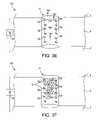
- FIGS. 1A–1Fillustrates a cross-sectional view of a resistance variable memory device fabricated in accordance with a first embodiment of the invention.
- FIGS. 2A–2Fillustrates a cross-sectional view of a resistance variable memory device fabricated in accordance with a second embodiment of the invention.
- FIGS. 3A–3Fillustrates a cross-sectional view of a resistance variable memory device fabricated in accordance with a third embodiment of the invention.
- FIGS. 4A–4Fillustrates a cross-sectional view of a resistance variable memory device fabricated in accordance with a fourth embodiment of the invention.
- FIG. 5illustrates a processor-based system having one or more memory devices that contains resistance variable memory elements according to the various embodiments of the invention.
- substrateused in the following description may include any supporting structure including but not limited to a glass, plastic, or semiconductor substrate that has an exposed substrate surface.
- a semiconductor substrateshould be understood to include silicon, silicon-on-insulator (SOI), silicon-on-sapphire (SOS), doped and undoped semiconductors, epitaxial layers of silicon supported by a base semiconductor foundation, and other semiconductor structures which may not be silicon-based.
- SOIsilicon-on-insulator
- SOSsilicon-on-sapphire
- doped and undoped semiconductorsepitaxial layers of silicon supported by a base semiconductor foundation, and other semiconductor structures which may not be silicon-based.
- metal-chalcogen regionssuch as silver-selenide, formed in a chalcogenide glass layer, for example, germanium-selenide
- a conditioning voltagecan be polarized upon application of a conditioning voltage and align to form a conducting channel within the chalcogenide glass layer.
- the conducting channelalters the resistance state of the glass from a very high resistance state, e.g. 1 G ⁇ , to a medium resistance state, e.g., 10 M ⁇ .
- a subsequently applied write voltagehaving an energy lower than that of the conditioning voltage, can then program the glass to a lower resistance state, e.g. 10k ⁇ , by causing available metal ions to move into the conducting channels where they remain after the write voltage is removed.
- the metal ions within the conducting channelcan be removed by application of a negative polarity erase voltage. Because the conducting channel is previously formed by the conditioning voltage before a write or erase operation occurs, higher speed switching of the glass between resistance states can be achieved compared to trying to form and completely decompose conductive pathways each time the glass is written or erased to a resistance state.
- the glass layercan be used to construct memory elements.
- memory elementsare described below in which a metal-chalcogen is described as silver-selenide, and the chalcogenide glass as germanium-selenide. However, these specific materials are not considered as limiting the invention.
- FIGS. 1A–F ; 2 A– 2 F; 3 A– 3 F; and 4 A– 4 -Frespectively illustrate exemplary embodiments of a resistance variable memory element 100 , 101 , 102 and 103 , and their methods of formation and operation, in accordance with the invention.
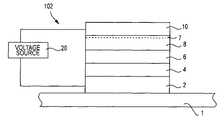
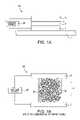
- FIG. 1Adepicts a first exemplary embodiment of a resistance variable memory element 100 and its method of formation in accordance with the invention.
- a first electrode 2is formed over a substrate 1 .
- the first electrode 2may comprise a conductive material, for example, various metals such as, one or more of tungsten, tantalum, aluminum, platinum, silver, or titanium nitride, among others.
- the first electrode 2can comprise a conductively-doped semiconductor material.
- the first electrode 2should preferably not produce or expel metal ions, as discussed below.
- FIG. 1Aillustrates a first electrode 2 provided on substrate 1
- additional layersmay be provided between electrode 2 and the substrate 1 .
- a barrier layermay be used to prevent migration of metal ions from layer 2 .
- a semiconductor substrate 1 containing circuit layers covered with an insulating layercan be provided below first electrode 2 if desired.
- the glass layer 4is formed over the first conductive electrode 2 .
- the glass layer 4is electrically coupled to electrode 2 .
- the glass layer 4is preferably a chalcogenide glass layer 4 that has been doped, e.g. photodoped, with a metal ion such as silver (Ag), and is more preferably a germanium-selenide glass layer 4 having a Ge x Se 100 ⁇ x stoichiometry doped with Ag ions.
- the stoichiometric range for glass layer 4is preferably from about Ge 18 Se 82 to about Ge 25 Se 75 , and is more preferably about Ge 25 Se 75 when metal ions, such as Ag ions, are provided in the glass layer 4 by a doping process.
- Glass layer 4is formed to a thickness of from about 150 ⁇ to about 600 ⁇ thick, and is preferably about 500 ⁇ thick.
- glass layer 4is described as a chalcogenide glass layer, other suitable glass layers may be employed as well.
- suitable glass material compositions for the glass layer 4can include, but are not limited to, AsSe (arsenic-selenide, such as As 3 Se 2 ), GeS (germanium-sulfide), and combinations of Ge, Ag, and Se, among others. Any one of the suitable glass materials for glass layer 4 and may further comprise small concentrations of dopants such as nitrogen nitrides, metals, and other group 13 – 17 elements from the periodic table.
- the formation of the chalcogenide glass layer 4 having a stoichiometric composition such as Ge 25 Se 75 in accordance with one exemplary embodiment of the inventioncan be accomplished by any suitable method. For instance, by evaporation, co-sputtering germanium and selenium in the appropriate ratios, sputtering using a germanium-selenide target having the desired stoichiometry, or chemical vapor deposition with stoichiometric amounts of GeH 4 and SeH 2 gases (or various compositions of these gases), which result in a germanium-selenide film of the desired stoichiometry, are some non-limiting examples of methods which can be used to form the glass layer 4 .
- metal ionsare doped into the glass layer 4 by a photodoping process.
- the chalcogenide glass layer 4such as Ge 25 Se 75
- a metalsuch as Ag.
- Metal ionscan be driven into the glass layer 4 by applying a metal (Ag) layer on top of the glass layer 4 and exposing the glass layer 4 and metal layer to visible radiation.
- the metal layercan be formed over the glass layer 4 , for example, by sputtering, physical vapor deposition, or other well-known techniques in the art.
- the metal doping of glass layer 4causes the glass layer 4 to contain polarizable metal-chalcogen regions 30 and glass backbone regions 50 , as shown in FIG. 1B .
- polarizable regionsare regions which can physically align in the presence of a suitable voltage applied across a memory element.
- the polarizable metal-chalcogen regions 30are distinct regions within the glass layer 4 .
- the glass layer 4will phase separate into polarizable metal-chalcogen regions 30 and glass backbone regions 50 .
- Maria Mitkova, et al.Dual Chemical Role of A as an Additive in Chalcogenide Glasses, P HYSICAL R EVIEW L ETTERS, Nov. 8, 1999, at 3848–3851.
- Agis used as the dopant metal ion and germanium selenide, e.g.
- the polarizable metal-chalcogen regions 30are Ag 2 Se regions within a germanium selenide backbone.
- the glass backbone regions 50are non-metal containing glass regions with a stoichiometry determined by the loss of selenium (Se) from the germanium selenide glass to the formation of Ag 2 Se.
- a second electrode 10is then formed over the glass layer 4 and any residual metal ions, e.g. Ag, remain in glass layer 4 to complete the formation of the resistance variable memory element 100 .
- the second electrode 10may comprise any conductive material, for example, various metals, such as, one or more of tungsten, tantalum, aluminum, platinum, silver, or titanium nitride among others.
- the second electrode 10can comprise a conductively-doped semi-conductive material, e.g., doped polysilicon.
- electrode 10may be directly applied to glass layer 4
- the second electrode 10is in contact with an intermediate metal-containing layer 5 , which is provided over glass layer 4 .
- This intermediate metal-containing layer 5is preferably a layer comprising Ag.
- the doping of metal, e.g., Ag, into the glass layer 4will produce metal ions used, e.g, Ag ions within glass layer 4
- the presence of the metal-containing layer 5will serve as an additional source and receptacle for metal ions during write and erase operations.
- the metal-containing layer 5can be Ag and is a source of metal ions, e.g., Ag, which enter glass layer 4 .
- the metal-containing layer 5is the receptacle of the metal ions, e.g., Ag that move out of the glass layer 4 .
- the metal containing layer 5is omitted and the top electrode 10 is formed of a material capable of donating and receiving metal ions.
- top electrode 10can be made of silver which would be in contact with glass layer 4 , and would then become a source and receptacle of metal ions during a write and erase operation. It is also possible to use an electrode 10 , which donates or receives metal ions with metal-containing layer 5 , which also donates or receives metal ions, in combination.
- first electrode 2 and the second electrode 10can comprise the same or different materials. However, for example, if the first electrode 2 and the second electrode 10 comprise the same material such as tungsten or any other non-metal ion comprising metal, one side of the memory element 100 , preferably the side with the second electrode 10 , must have an excess of metal ions, e.g., Ag which, in the preferred embodiment, is metal-containing layer 5 .
- metal ionse.g., Ag which, in the preferred embodiment, is metal-containing layer 5 .
- electrode 2Because the metal ions, e.g., Ag ions which enter and leave glass 4 comes from layer 5 , if provided, or layer 10 , if layer 5 is not provided, it is preferable that electrode 2 not donate any metal ions. As a result, although intervening barrier layers are not illustrated in the FIG. 1A embodiment, intervening barrier layers can be present to prevent metal ion migration from electrode 2 into glass layer 4 , or from electrode 10 into glass layer 4 . The barrier layers, if provided, should not contain mobile metal ions.
- FIGS. 1B–1FA method of operating and manipulating the resistance state of the memory element depicted in FIG. 1A will now be described in reference to FIGS. 1B–1F .
- FIG. 1Bis a cross-sectional view of the memory element 100 of FIG. 1A prior to application of a conditioning voltage.
- the chalcogenide glass regions 50 and polarizable metal-chalcogen regions 30have no long range order, i.e., they are randomly distributed.
- the doped chalcogenide glass layer 4contains regions of germanium-selenide 50 and regions of polarizable silver-selenide 30 . Free Ag ions may also be present in glass layer 4 .
- the germanium-selenide regions 50serve as the glass backbone for memory element 100 .
- V 1a conditioning voltage of suitable energy, for example, is applied from a voltage source (DC) 20 .
- DCvoltage source
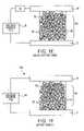
- one or more regions of silver-selenide 30will polarize, that is, align to form a conducting channel 60 .
- the aligned silver-selenide regions 40form conducting channel 60 which spans the entire thickness of glass layer 4 .
- the application of V 1induces the alignment of the polarizable silver-selenide regions. It has been found that a conditioning voltage (V 1 ) about 200 mV under DC switching conditions and about 1.7V, 500 ns under AC conditions, is sufficient to physically align the Ag 2 Se regions 30 and form the conducting channel 60 .
- memory element 100After the conditioning voltage V 1 is applied, memory element 100 is in a ‘medium’ state of resistance. Prior to application of the conditioning voltage illustrated in FIG. 1B , the memory element 100 is in a ‘high’ state of resistance. As a non-limiting example, a ‘high’ state of resistance for memory element 100 can be greater than 1 G ⁇ . A ‘medium’ state of resistance, produced by the alignment of the Ag 2 Se regions 30 can be around 1 M ⁇ .
- FIG. 1Cillustrates the memory element 100 in the ‘medium’ state of resistance after applying a conditioning voltage V 1 .
- the conditioning voltage V 1is at a higher potential than subsequent potentials used to write, read, or erase the memory element 100 . This is due to the initial disorder of the polarizable silver-selenide regions 30 , as illustrated in FIG. 1B . Prior to application of the conditioning voltage V 1 , the structure of the memory element 100 is in the most disordered state. Thus, to bring the memory element 100 into a more structured state illustrated in FIG. 1C , a conditioning voltage V 1 which is larger than subsequently applied write, erase or read voltages is required.
- the amplitude of V 1necessary to induce formation of conducting channel 60 , will depend upon the pulse width, glass layer 4 composition, and thickness.
- a 1.7V pulse having a duration of 500 nswas found to be sufficient.
- the pre-established conducting channel 60allows additional metal ions within the glass layer 4 , or from the metal-containing layer 5 , and/or electrode 10 , to move into and out of the conducting channel 60 upon application of a potential across the two electrodes.
- the resistance state of the memory element 100can be changed quickly.
- the movement of the Ag ions in the conducting channel 60 upon application of a write voltage V 2which has a potential less than the conditioning voltage V 1 , can lower the resistance state of the memory element 100 from the medium resistance state of e.g., 1 M ⁇ , to a lower resistance state of e.g., 10 k ⁇ .
- the silver ionsare driven out of the conducting channel 60 and back into the glass layer 4 and metal-containing layer 5 , and/or electrode 10 , increasing the resistance state of the memory element 100 back to the medium resistance state.
- the erase voltageneed only be sufficient to drive Ag ions out of the conducting channel 60 .
- the conducting channel 60is not dispersed and is still maintained.
- the switching speeds and response of the memory element 100are enhanced because the Ag ions can move into and out of the conducting channel 60 without the need to reform the channel 60 every time the memory element 100 is switched.
- germanium-selenide regions 50serve to isolate the polarizable metal-chalcogen regions 30 from each other, here, polarizable silver-selenide regions 30 .
- the germanium-selenide regions 50also restrict the mobility and provide isolation between the polarized silver-selenide regions 40 .
- conducting channel 60may be formed in glass layer 4 .
- conditioning of the memory element 100is conducted only once, and after the memory element 100 is conditioned, the conditioned structure 100 will operate through normal write and erase operations.
- FIG. 1Dillustrates the memory element 100 after a write operation is performed.
- a write voltage V 2is applied from a voltage source 20 , to ‘write’ information into the resistance variable memory element 100 .
- the write voltage V 2occurs at a lower potential than the conditioning voltage V 1 .
- the conditioning pulseis 200 mV
- memory element 100should be written with a ‘write’ voltage V 2 of less than 200 mV.
- the additional Ag ionsenter the pre-established conductive channel 60 to further complete the conductive path and lower the resistance of the memory element 100 .
- FIG. 1Dillustrates memory element 100 in the ‘low’ state of resistance, e.g., around 10 k ⁇ .
- the pre-established conductive channels 60may be affected by high temperatures as the metal ions and polarizable metal-chalcogen regions 30 become more mobile. Accordingly, when this occurs, it may be desirable to periodically refresh the memory elements by periodically reapplying the conditioning pulse V 1 to reset the conductive channel 60 and thereby resetting the memory element 100 to its medium resistance state.
- a ‘read’ operationis illustrated in which a read potential V 3 , which is less than write potential V 2 , is applied to the memory element 100 .
- Current flow through the memory element 100is sensed by a current sensing amplifier 32 , which provides an output representing the resistance state of the memory element 100 .
- a read voltage V 3which is below the threshold for writing the memory element 100 , e.g., V 2 , is sufficient. Where the write voltage V 2 is about 700 mV with a pulse duration of 100 ns, the read voltage V 3 can then be a potential less than about 200 mV with a pulse width less than about 500 ns. The read voltage V 3 does not disturb other memory elements in a memory element array, which are in the pre-conditioned medium resistance ‘OFF’ state, since the read voltage V 3 is lower than the write voltage V 2 .
- the read voltage V 3may be applied in various manners, such as a sweep voltage, pulse voltage, or step voltage, among other methods.
- FIG. 1Fillustrates the memory element 100 when an erase voltage is applied across the electrodes 2 and 10 from voltage source 20 .
- An erase voltage V 4 having an inverse polarity from the write voltage V 2is applied from electrode 10 to electrode 2 to erase the memory element 100 .
- the erase voltage V 4may also be of a smaller absolute magnitude than the write voltage V 2 .
- an erase voltage V 4moves Ag ions out of the conducting channel 60 toward the electrode with the negative potential. This is electrode 10 in FIG. 1F .
- the Ag ionswill move out of the conducting channel 60 and into the metal-containing layer 5 , the glass layer 4 , and/or electrode 10 if the electrode 10 contains Ag.
- the eraseis essentially a function of removing Ag ions from conducting channel 60 .
- the eraseis complete when the resistance of the memory element 100 returns to the ‘medium’ state of resistance, i.e., around 1 M ⁇ .
- the conducting channel 60 of FIG. 1Cremains intact; thus, allowing for faster write and erase switching times.
- the erase voltage V 4returns the memory element 100 to the state of resistance illustrated in FIG. 1C .
- the erase voltage V 4should be low enough to cause a resistance shift in the memory element 100 , but not of a magnitude which would destroy the conducting channel 60 .
- the conditioning, write, and erase pulse widthsare dependent on the electric field amplitude, i.e., the applied voltage.
- shorter pulseswill require higher voltages for V 1 , V 2 , and V 4 and vice versa.
- Thisis expected since the movement of Ag ions in the conducting channel 60 has an energy requirement for movement into and out of the conducting channel 60 , which in turn is dependent upon the concentration of Ag ions which enters or leaves the conducting channel 60 .
- FIG. 2Ashows another exemplary embodiment of the invention and its method of formation.
- the FIG. 2A embodimenthas a first electrode 2 formed over a substrate 1 .
- the first electrode 2may comprise any of the conductive materials listed above for the same electrode as in the FIG. 1A embodiment.
- additional barrier layersmay be provided between electrode 2 and substrate 1 , if required to prevent metal ion migration.
- the barrier layers, if provided,should not contain mobile metal ions.
- a glass layer 4such as a chalcogenide glass layer 4 is formed over the first electrode 2 .
- the glass layer 4is electrically coupled to electrode 2 .
- the glass layer 4is preferably a chalcogenide glass layer 4 , and more preferably, a germanium-selenide glass layer 4 having a Ge x Se 100 ⁇ x stoichiometry.
- the stoichiometric range for chalcogenide glass layer 4 as depicted in the FIG. 2A embodimentis preferably from about Ge 20 Se 80 to about Ge 43 Se 57 , and is more preferably about Ge 40 Se 60 .
- Glass layer 4is formed to a thickness of from about 150 ⁇ to about 500 ⁇ thick, and preferably is about 150 ⁇ thick.
- the glass layer 4 of structure 101is described further below as a chalcogenide glass layer 4 and more specifically, a Ge 40 Se 60 layer.
- suitable glass or polymer layersmay be employed without affecting the utility of the invention.
- suitable glass material compositions for the glass layer 4can include but are not limited to, SiSe (silicon-selenide), AsSe (arsenic-selenide, such as As 3 Se 2 ), GeS (germanium-sulfide), and combinations of Ge, Ag, and Se, among others.
- Any one of the suitable glass materialsmay further comprise small concentrations of dopants such as nitrogen nitrides, metals, and group 1 , 2 , and 13 – 17 elements from the periodic table.
- the formation of the glass layer 4 having a stoichiometric composition such as Ge 40 Se 60 in accordance with one exemplary embodiment of the inventioncan be accomplished by any suitable method. For instance, evaporation, co-sputtering germanium and selenium in the appropriate ratios, sputtering using a germanium-selenide target having the desired stoichiometry, or chemical vapor deposition with stoichiometric amounts of GeH 4 and SeH 2 gases (or various compositions of these gases), which result in a germanium-selenide film of the desired stoichiometry, are some non-limiting examples of methods which can be used to form the glass layer 4 . It should be appreciated that the glass layer 4 may comprise one or more layers of a glass material.
- a metal-containing layer 6preferably silver-selenide, is deposited over the chalcogenide glass layer 4 .
- any suitable metal-containing layer 6may be used so long as it interacts with the glass backbone such that it allows the transfer of metal ions into glass layer 4 upon application of a sufficient voltage across a memory element of which layers 4 and 6 are a part.
- the metal-containing layer 6may comprise silver, copper, or other transition metals.
- Other suitable metal-containing layers 6 which may be usedinclude glass layers doped with a metal.
- the metal-containing layer 6will comprise the same type of chalcogen component as is present in glass layer 4 .
- glass layer 4is Ge x Se 100 ⁇ x
- metal-containing layer 6may be Ag 2 Se.
- the metal-containing layer 6is formed to a thickness of from about 300 ⁇ to about 1200 ⁇ thick, and preferably is about 470 ⁇ thick.
- metal-containing layer 6can be formed to contain excess metal ions. That is, Ag 2+x Se, where x represents excess Ag ions.
- a separate second metal-containing layer 7 with a sufficient thickness that gives the desired excess amount of metal ions, e.g., Ag ions to the metal-containing layer 6may be provided over or beneath the first metal-containing layer 6 .
- Electrode 10is provided over the conducting metal-containing layer 6 , if metal-containing layer 7 is omitted, or is provided over metal-containing layer 7 if the latter is provided. Electrode 10 need not donate any metal ions if one or both of layers 6 and 7 provide sufficient metal ions for memory element operation.
- the second metal-containing layer 7is provided and serves as a source and receptacle for metal ions doing write and erase operations.
- the top electrode 10may be the source and receptacle of additional metal ions when the second metal-containing layer 7 is omitted, and excess metal ions are not available in layer 6 .
- the top electrode 10may comprise silver, which donates and receives silver ions to and from glass layer 4 .
- the metal-containing layer 6Some non-limiting examples of forming the metal-containing layer 6 are physical vapor deposition techniques such as evaporative deposition, sputtering, chemical vapor deposition, co-evaporation, or depositing a layer of selenium above a layer of silver to form silver-selenide (Ag 2 Se) can also be used. It should be appreciated that the metal-containing layer 6 may comprise one or more layers of a metal-containing material. For purposes of a simplified description, FIGS. 2A–2F refer to the first metal-containing layer 6 as a silver-selenide layer 6 and the second metal-containing layer 7 as a silver layer 7 . In this case electrode 10 does not contribute metal ions to, or receive metal ions from glass layer 4 .
- the second electrode 10may comprise any of the materials described above for electrode 10 of the FIG. 1A embodiment.
- FIG. 2Aillustrates that the second electrode 10 is in contact with an upper surface of the second metal-containing layer 7 ; however, intervening layers may be provided between layers 7 and 10 , if desired.
- the second metal-containing layer 7can provide additional Ag ions.
- the second electrode 10can comprise Ag which can also provide additional Ag ions if the second metal-containing layer 7 is omitted from memory element 101 .
- the metal containing layer 7is omitted and the top electrode 10 , which is in contact with metal-containing layer 6 , can provide and receive metal ions, e.g., Ag ions, and can be the source and receptacle of metal ions during a write and erase operation. It is also possible to use an electrode 10 , which donates or receives metal ions with metal-containing layer 7 , which also donates or receives metal ions in combination. It should be appreciated that the first electrode 2 and the second electrode 10 can comprise the same or different materials.
- the first and second metal-containing layers 6 and 7can provide Ag ions.
- the second electrode 10can comprise Ag, if used, which can also provide Ag ions if the second metal-containing layer 7 is omitted from memory element 101 , and layer 6 does not have excess Ag ions. Because the metal ions, e.g., Ag ions which enter and leave glass 4 is coming from the second metal-containing layer 7 , if provided, or electrode 10 , if layer 7 is not provided and layer 6 does not have excess Ag ions., it is preferable that electrode 2 not donate any metal ions
- intervening barrier layersare not illustrated in the FIG. 2A embodiment, intervening barrier layers can be present to prevent metal ion migration from electrode 2 into glass layer 4 , or from electrode 10 into glass layer 4 .
- Barrier layersif provided, should not contain mobile metal ions.
- FIGS. 2B–2FA method of operating and manipulating the resistance state of the memory element 101 depicted in FIG. 2A will now be described in reference to FIGS. 2B–2F .
- the methods of operation described in FIGS. 2B–2Fis for a memory element 101 comprising a Ge 40 Se 60 glass layer 4 that is 150 ⁇ thick, an Ag 2 Se layer 470 ⁇ thick, and a silver layer 200 ⁇ thick.
- FIG. 2Bis a cross-sectional view of the glass layer 4 in memory element 101 of FIG. 2A prior to application of a conditioning voltage across memory element 101 .
- the germanium-selenide glass layer 4has no long range order, i.e., it has non-uniform distribution of Ge and Se within the glass layer 4 .
- FIG. 2Bfurther illustrates the presence of germanium-germanium (Ge—Ge) bonds 17 throughout the glass layer 4 .
- Ge—Gegermanium-germanium
- a conditioning pulse having a potential V 1is applied across memory element 101 .
- the conditioning pulsecauses metal chalcogenide, e.g., Ag 2 Se from the layer 6 to enter into glass layer 4 , thereby breaking Ge—Ge bonds 17 in the glass layer 4 and to form conductive channel 11 within the glass 4 backbone.
- the conditioning pulse's parametersare dependent upon the composition and thickness of the various layers comprising memory element 101 .
- a conditioning pulsehaving a pulse duration from about 10 to about 500 ns and greater than about 700 mV has been found sufficient to form conductive channel 11 .
- the amplitude of the conditioning pulsewill depend on the pulse width.
- the conducting channel 11will form in the weakest part of the chalcogenide glass material 4 , i.e., in the areas that require the least amount of energy to form the conductive channel 11 .
- the conditioning pulsecauses the conducting channel 11 to form by re-orientation of the GeSe and Ag 2 Se regions, as shown in FIG. 2C .
- a plurality of conducting channels 11can be formed in the chalcogenide glass layer 4 . For purposes of a simplified description, only one conducting channel 11 is illustrated in FIGS. 2C–2F .
- memory element 101After application of the conditioning pulse, memory element 101 is in a “medium” state of resistance. Prior to application of a conditioning pulse, and as illustrated in FIG. 2B , memory element 101 is in a ‘high’ state of resistance where the germanium-selenide regions are not oriented. For instance, a ‘high’ state of resistance which arises after the conditioning pulse is applied to memory element 101 can be about 1 G ⁇ . A ‘medium’ state of resistance can be around 1 M ⁇ .
- the memory element 101In the medium resistance state, the memory element 101 is still considered ‘OFF’ and remains in this conditioned state, with the Ag 2 Se regions, polarized and aligned in the direction of current flow, until the conducting channel 11 receives excess metal ions from the first metal-containing layer 6 , if excess metal ions are present, and from the second metal containing layer 7 , and/or electrode 10 during a ‘write’ operation.
- applying a conditioning pulse across the memory element 101breaks the weak Ge—Ge bonds 17 within the Ge 40 Se 60 glass layer 4 and allows Ag 2 Se and ions thereof to bond to germanium-selenide sites.
- the conditioning pulse V 1reorients the non-uniform state of the chalcogenide glass layer 4 ( FIG. 2B ) into a more organized and structured state having aligned Ag 2 Se areas as illustrated in FIG. 2C .
- the memory element 101 of FIG. 2Cis still in a medium or ‘OFF’ state of resistance.
- One exemplary write potential V 2is preferably a pulse from about 8 to about a 150 ns that is less than the potential of V 1 , e.g., less than 700 mV.
- a write potential V 2 of about 400 mVhas been found to be adequate with the memory element 101 .
- the amplitude of the write potentialwill vary depending on the pulse width.
- the Ag ionstake the path of least resistance into glass layer 4 .
- the path of least resistanceis provided by the conducting channel 11 .
- the Ag ionswill migrate toward the negative potential, here, electrode 2 , when applied across the memory element 101 . Accordingly, the movement of the Ag ions into the conducting channel 11 renders channel 11 more conductive.
- An exemplary erase potential V 4is a pulse from about 8 to about 150 ns that is from about negative 400 mV ( ⁇ 400 mV) to about negative 700 mV ( ⁇ 700 mV) in amplitude. As with the write potential V 2 , the amplitude of the erase potential V 4 will depend on the pulse width.
- a 10 ns, 1.7V conditioning pulse V 1was applied to cause the memory element 101 , initially at 1 G ⁇ , to move into a ‘medium’ state of resistance of approximately 1 M ⁇ .
- a 10 ns, 700 mV write pulse V 2was applied to the memory element 101 to move it to a low resistance state of approximately 10 k ⁇ .
- a 10 ns, negative 550 mV erase pulse V 4was applied to return the memory element 101 to a medium resistance state. It was also observed that applying a 10 ns, 700 mV write pulse V 3 repeatedly to the memory element 101 yielded lower and lower resistance states below 10 k ⁇ .
- the memory element 101could be used to set different detectable logic states in accordance with the number of applied write pulses V 3 .
- a ‘read’ operationin which a read potential V 5 , which is less than write potential V 2 , can applied to the memory element 101 .
- Current flow through the memory element 101can be sensed by a current sensing amplifier, which can provide an output representing the resistance state of the memory element 101 (not pictured).
- a read voltage V 5which is below the threshold for writing the memory element 101 , e.g., V 1 , is sufficient. Where a 10 ns, 700 mV write pulse V 2 is used, the read voltage V 5 can then be in the range from any pulse less than about 500 ns and less than or equal to about 200 mV. The read voltage V 5 does not disturb other memory elements in a memory element array, which are in the pre-conditioned medium resistance ‘OFF’ state, since the read voltage V 5 is lower than the write voltage V 2 .
- the read voltage V 5may be applied in various manners, such as a sweep voltage, pulse voltage, or step voltage, among other methods.
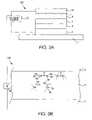
- FIG. 3A-3Fdepicts a third exemplary embodiment of a resistance variable memory device 102 constructed in accordance with the invention.
- a first electrode 2is formed over a substrate 1 .
- the first electrode 2may comprise any of the conductive materials listed above as in the FIGS. 1A and 2A embodiments.
- a first glass layer 4is formed over the first electrode 2 .
- the first glass layer 4is electrically coupled to electrode 2 .
- the first glass layer 4can comprise the same materials as in prior embodiments and have the same stoichiometric ranges as the glass layer 4 in FIG. 2A .
- the first glass layer 4is described further below as a Ge 40 Se 60 chalcogenide glass layer 4 .
- Glass layer 4is formed to a thickness of from about 150 ⁇ to about 500 ⁇ thick, and preferably is about 150 ⁇ thick.
- the formation of the chalcogenide glass layer 4having a stoichiometric composition, such as Ge 40 Se 60 , can be accomplished by any of the methods described above for forming the glass layer 4 of FIG. 2A .
- the first glass layer 4may comprise one or more layers of a glass material.
- a first metal-containing layer 6preferably silver-selenide, is formed over the first chalcogenide glass layer 4 .
- the formation of the first metal-containing layer 6can be accomplished by any of the methods described above for forming the metal-containing layer 6 of FIG. 2A .
- the first metal-containing layer 6may comprise one or more layers of a metal-containing material.
- the first metal-containing layer 6is formed to a thickness of from about 300 ⁇ to about 1200 ⁇ thick, and preferably is about 470 ⁇ thick.
- a second glass layer 8is formed over the first metal-containing layer 6 .
- the second glass layer 8allows deposition of silver above a silver-selenide layer 6 , for instance.
- the second glass layer 8can be utilized as a diffusion control layer to prevent metal ions from migrating from electrode 10 into the memory element 102 .
- the second glass layer 8is formed to a thickness of from about 100 ⁇ to about 300 ⁇ thick, and preferably is about 150 ⁇ thick.
- the formation and composition of the second glass layer 8is the same as described above for the formation and composition of the glass layer 4 of FIG. 3A .
- the second glass layer 8is described as a chalcogenide glass layer having a stoichiometry similar to the first glass layer 4 i.e., Ge 40 Se 60 .
- one or more layers of glass materialcan be provided if desired for glass layer 8 .
- the second glass layer 8may be formed to a thickness of from about 100 ⁇ to about 300 ⁇ thick, and preferably is about 150 ⁇ thick.
- first glass layer 4 and the second glass layer 8are described above as having a stoichiometry and material composition similar to each other i.e., Ge 40 Se 60 , it should be appreciated that the first glass layer 4 and the second glass layer 8 can possess different stoichiometries from each other, different thicknesses, and they can even be formed of different glasses.
- excess metal ionsneed to be provided in this embodiment as well, either by excess metal ions in the first metal-containing layer 6 , by an optional second metal-containing layer 7 provided above glass layer 8 , or by upper electrode 10 .
- the first metal-containing layer 6can be formed containing excess metal ions.
- the excess metal ionsare not part of the first metal-containing layer 6 , i.e., added specifically or deposited with an excess metal, the metal ions need to be added as a separate second metal-containing layer 7 and/or an upper electrode 10 .
- the second metal-containing layer 7should have a sufficient thickness that gives the desired excess amount of metal ions to the glass layer 4 .
- the second metal-containing layer 7can comprise any metal ions so long as it provides metal ions to enable formation of a conducting channel in the glass layer 4 after application of a conditioning pulse.
- the second metal-containing layer 7may comprise silver or copper.
- the second metal-containing layer 7is present and serves as a source and receptacle for additional metal ions.
- a second electrode 10is formed over the second glass layer 8 or over the second metal containing layer 7 , if provided, as shown in FIG. 3A , to complete the formation of the memory element 102 .
- the second electrode 10may comprise any of the conductive materials listed above for the electrode 10 described in reference to FIGS. 1A and 2A .
- FIG. 3Aillustrates that the second electrode 10 is in contact with an upper surface of the second metal-containing layer 7 ; however, intervening layers may be provided between layers 7 and 10 , if desired.
- the second metal-containing layer 7can provide additional Ag ions.
- the second electrode 10can comprise Ag which can also provide additional Ag ions if the second metal-containing layer 7 is omitted from structure 102 .
- first electrode 2 and the second electrode 10can comprise the same or different materials. However, for example, if the first electrode 2 and the second electrode 10 comprise the same material, such as tungsten or any other non-metal ion comprising metal, one side of the memory element 102 , preferably the side with the second electrode 10 , must have an excess of metal ions, Ag in the preferred embodiment, either in layer 6 or preferably as the second metal-containing layer 7 .
- intervening barrier layersare not illustrated in the FIG. 3A embodiment, intervening barrier layers can be present to prevent metal ion migration from electrode 2 into glass layer 4 , or from electrode 10 into glass layer 4 , when the excess metal ions are provided by layers 6 and/or 7 . Barrier layers, if provided, should not contain mobile metal ions.
- FIGS. 3B–3FA method of operating and manipulating the resistance state of the memory element 102 depicted in FIG. 3A is described below in reference to FIGS. 3B–3F .
- the methods of operation described in FIGS. 3B–3Fis for a memory element 102 comprising a first Ge 40 Se 60 glass layer 4 that is 150 ⁇ thick, an Ag 2 Se layer 470 ⁇ thick, a second Ge 40 Se 60 glass layer 8 that is 150 ⁇ thick and a silver layer 200 ⁇ thick.
- FIG. 3Bis a cross-sectional view of the glass layer 4 of memory element 102 of FIG. 3A prior to application of a conditioning pulse V 1 .
- the glass layer 4formed of Ge 40 Se 60 , has no long range order.
- FIG. 3Bfurther illustrates the presence of germanium-germanium (Ge—Ge) bonds 17 throughout the glass layer 4 .
- Ge—Gegermanium-germanium
- the presence of another species which can provide a more thermodynamically favorable energywill break the Ge—Ge bonds 17 and bond with the previously bonded Ge. Accordingly, the Ge—Ge bond 17 is not strong and can easily be broken.
- a conditioning pulse V 1when a conditioning pulse V 1 is applied across memory element 102 , excess Ag ions from the first and/or second metal-containing layers 6 , 7 and/or from electrode 10 (if ions are available), enter into glass layer 4 and break some of the Ge—Ge bonds 17 . This forms conducting channel 11 via incorporation of Ag 2 Se from the first metal-containing layer 6 and is illustrated in FIG. 3C .
- the conditioning pulse's V 1 parametersare dependent upon composition and thickness of the layers comprising memory element 102 .
- the methods of operating memory element 101 depicted in FIGS. 2C–2Fis similar to the methods of operating memory element 102 for write, read and erase operations.
- the methods of operating memory element 102can proceed in a similar manner as illustrated in FIGS. 3C–3F .
- FIG. 4Adepicts a fourth exemplary embodiment of a resistance variable memory device 103 constructed in accordance with the invention.
- a first electrode 2is formed over a substrate 1 .
- the first electrode 2may comprise any of the conductive materials listed above for the electrode 2 described in the FIGS. 1A , 2 A and 3 A embodiments.
- a first glass layer 4is formed over the first electrode 2 .
- the first glass layer 4is electrically coupled to electrode 2 .
- the first glass layer 4can comprise the same material as provided for the glass layer 4 in FIGS. 2A and 3A .
- the first glass layer 4is described further below as a Ge 40 Se 60 chalcogenide glass layer 4 .
- the formation of the first chalcogenide glass layer 4can be accomplished by any of the methods described above for forming the glass layer 4 of FIGS. 2A and 3A .
- the first glass layer 4may comprise one or more layers of a glass material.
- the first glass layer 4is formed to a thickness of from about 150 ⁇ to about 500 ⁇ thick, and preferably is about 150 ⁇ thick.
- a first metal-containing layer 6preferably silver-selenide, is formed over the first chalcogenide glass layer 4 .
- the formation of the first metal-containing layer 6can be accomplished by any of the methods described above for forming the metal-containing layer 6 of FIGS. 2A and 3A .
- the first metal-containing layer 6may comprise one or more layers of a metal-containing material.
- the first metal-containing layer 6is formed to a thickness of from about 300 ⁇ to about 1200 ⁇ thick, and preferably is about 470 ⁇ thick.
- a second glass layer 8is formed over the first metal-containing layer 6 .
- the second glass layer 8may be used as a diffusion control layer to control the migration of metal ions into the glass layer 4 .
- the formation and composition of the second glass layer 8is the same as described above for the formation and composition of the glass layer 4 of FIGS. 2A and 3A .
- the second glass layer 8is described as a chalcogenide glass layer having a stoichiometry similar to the first glass layer 4 e.g., Ge 40 Se 60 . Further, one or more layers of glass material can be provided if desired.
- first glass layer 4 and the second glass layer 8are described above as having a stoichiometry and material composition similar to each other, e.g., Ge 40 Se 60 , it should be appreciated that the first glass layer 4 and the second glass layer 8 can possess different stoichiometries from each other, be different thicknesses, and they can even be different glasses.
- the second glass layer 8may be formed to a thickness of from about 100 ⁇ to about 300 ⁇ thick and preferably is about 150 ⁇ thick.
- a second metal-containing layer 9preferably silver is formed over the second glass layer 8 .
- the formation of the second metal-containing layer 9can be accomplished by any of the methods described above for forming the metal-containing layer 6 of FIGS. 2A and 3A .
- the second metal-containing layer 9may comprise one or more layers of a metal-containing material.
- the second metal-containing layer 9is formed to a thickness of from about 100 ⁇ to about 500 ⁇ thick, and preferably is about 200 ⁇ thick.
- excess metal ionsneed to be provided either by the first metal-containing layer 6 or second metal-containing layer 9 , and/or second electrode 10 .
- the first metal-containing layer 6can be formed containing excess metal ions.
- the excess metal ionsare not part of the first metal-containing layer 6 i.e., added specifically or deposited with an excess metal, the additional metal ions can be provided from the second metal-containing layer 9 and/or second electrode 10 .
- the second metal-containing layer 9should have a sufficient thickness that gives the desired excess amount of metal ions to the first metal-containing layer 6 .
- a third metal-containing layer 7can be provided, if desired.
- the third metal-containing layercomprises silver.
- the second metal-containing layer 9can comprise any metal ions so long as it provides metal ions to the conducting channel 11 formed in the chalcogenide glass layer 4 after application of a conditioning voltage across the electrodes 2 and 10 .
- the presence of the third metal-containing layer 7serves as the source and receptacle for metal ions.
- the third metal-containing layer 7is the source of the metal ions that move into the conducting channel 11 .
- the third metal-containing layer 7is the receptacle of the metal ions that move out of the conducting channel 11 .
- a second electrode 10is next formed over the third metal-containing layer 7 , as illustrated in FIG. 4A , to complete the formation of the memory device 103 .
- the second electrode 10may comprise any of the conductive materials listed above for the electrode 10 as described above in the FIGS. 2A and 3A embodiments.
- FIG. 4Aillustrates that the second electrode 10 is in contact with an upper surface of the third metal-containing layer 7 ; however, intervening layers may be provided between layers 7 and 10 , if desired.
- the third metal-containing layer 7can provide additional Ag ions.
- the second electrode 10can comprise Ag which can also provide additional Ag ions if the third metal-containing layer 7 is omitted from memory element 103 .
- the third metal containing layer 7is omitted and the second metal-containing layer 9 , can provide and receive metal ions, e.g., Ag ions, and can be the source and receptacle of metal ions during a write and erase operation. It is also possible to use an electrode 10 , which donates or receives metal ions with the third metal-containing layer 7 or second metal-containing layer 9 , which also donates or receives metal ions in combination.
- metal ionse.g., Ag ions
- first electrode 2 and the second electrode 10can comprise the same or different materials. However, for example, if the first electrode 2 and the second electrode 10 comprise the same material such as tungsten or any other non-metal ion comprising metal, one side of the memory element 103 , preferably the side with the second electrode 10 , must have an excess of metal ions, e.g., Ag.
- the third metal-containing layer 7can provide Ag ions or the second metal-containing layer 9 can.
- the second electrode 10can comprise Ag, if used, which can also provide Ag ions if the third metal-containing layer 7 is omitted from memory element 103 , if desirable. Because the metal ions, e.g., Ag ions which enter and leave glass 4 is coming from the third metal-containing layer 7 , if provided, or layer 10 , or layer 9 , if layer 7 is not provided, it is preferable that electrode 2 not donate any metal ions
- intervening barrier layersare not illustrated in the FIG. 4A embodiment, intervening barrier layers can be present to prevent metal ion migration from electrode 2 into glass layer 4 , or from electrode 10 into glass layer 4 .
- Barrier layersif provided, should not contain mobile metal ions.
- FIGS. 4B–4FA method of operating and manipulating the resistance state of the memory element depicted in FIG. 4A is described below in reference to FIGS. 4B–4F .
- the methods of operation described in FIGS. 4B–4Fis for a memory element 103 comprising a first Ge 40 Se 60 glass layer 4 that is 150 ⁇ thick, a first Ag 2 Se layer 470 ⁇ thick, a second Ge 40 Se 60 glass layer 8 that is 150 ⁇ , a second Ag 2 Se layer 200 ⁇ thick, and a silver layer 300 ⁇ thick.
- FIG. 4Bis a cross-sectional view of the memory element 103 of FIG. 4A prior to application of a conditioning pulse.
- the Ge 40 Se 60 glass layer 4has no long range order.
- FIG. 4Bfurther illustrates the presence of germanium-germanium (Ge—Ge) bonds 17 throughout the glass layer 4 .
- Ge—Gegermanium-germanium
- the presence of another species which can provide a more thermodynamically favorable energy than the Ge—Ge bond energywill break the Ge—Ge bonds 17 and bond with the previously bonded Ge. Accordingly, the Ge—Ge bonds 17 are not strong and can easily be broken.
- a conditioning pulse VIis applied to memory element 103 .
- Memory element 103is conditioned in a similar manner as described above with regard to memory elements 101 and 102 . Conditioning the memory element 103 , is done only once and after the memory element 103 is conditioned, the conditioned memory element 103 will operate through normal write and erase operations.
- applying a conditioning pulse from the voltage source 20forms a conducting channel 11 via incorporation of Ag 2 Se from the metal-containing layer 6 into the glass backbone which is illustrated in FIG. 4C .
- the Ag 2 Sebecomes polarized and aligned within the glass 4 backbone to form conductive channel 11 .
- the conditioning pulse's parametersare dependent upon the thickness of the layers comprising memory element 103 .
- the method of operating memory element 103 depicted in FIGS. 4C–4Fproceeds in an analogous manner as described above with reference to FIGS. 2C–2F and 3 C– 3 F.
- the presence of an additional metal-containing layer 7which provides the Ag ions, can enhance the switching characteristics of the memory elements 101 , 102 and 103 . For instance, since there are more available Ag ions to move in and out of the pre-formed conducting channels 11 , the memory elements 101 , 102 and 103 can operate with greater speed.
- FIGS. 1A–4Frefer to the formation of only one resistance variable memory element 100 , 101 , 102 and 103 , it must be understood that the invention contemplates the formation of any number of such memory elements.
- a plurality of resistance variable memory elementscan be fabricated in a memory array and operated with memory access circuits.
- the resistance variable memory elements 100 , 101 , 102 and 103can be utilized in many electronic devices.
- the methods and operation of the memory elements disclosed hereincan be used in any device whenever it is desired to have a resistance variable memory element with faster switching times.
- the resistance variable memory elements 100 , 101 , 102 and 103 of the inventionmay be used in memory applications as well as in creating various CMOS type circuits.
Landscapes
- Engineering & Computer Science (AREA)
- Manufacturing & Machinery (AREA)
- Semiconductor Memories (AREA)
Abstract
Description
Claims (46)
Priority Applications (2)
| Application Number | Priority Date | Filing Date | Title |
|---|---|---|---|
| US10/765,393US7153721B2 (en) | 2004-01-28 | 2004-01-28 | Resistance variable memory elements based on polarized silver-selenide network growth |
| US11/149,225US20050286294A1 (en) | 2004-01-28 | 2005-06-10 | Resistance variable memory elements based on polarized silver-selenide network growth |
Applications Claiming Priority (1)
| Application Number | Priority Date | Filing Date | Title |
|---|---|---|---|
| US10/765,393US7153721B2 (en) | 2004-01-28 | 2004-01-28 | Resistance variable memory elements based on polarized silver-selenide network growth |
Related Child Applications (1)
| Application Number | Title | Priority Date | Filing Date |
|---|---|---|---|
| US11/149,225DivisionUS20050286294A1 (en) | 2004-01-28 | 2005-06-10 | Resistance variable memory elements based on polarized silver-selenide network growth |
Publications (2)
| Publication Number | Publication Date |
|---|---|
| US20050162907A1 US20050162907A1 (en) | 2005-07-28 |
| US7153721B2true US7153721B2 (en) | 2006-12-26 |
Family
ID=34795469
Family Applications (2)
| Application Number | Title | Priority Date | Filing Date |
|---|---|---|---|
| US10/765,393Expired - Fee RelatedUS7153721B2 (en) | 2004-01-28 | 2004-01-28 | Resistance variable memory elements based on polarized silver-selenide network growth |
| US11/149,225AbandonedUS20050286294A1 (en) | 2004-01-28 | 2005-06-10 | Resistance variable memory elements based on polarized silver-selenide network growth |
Family Applications After (1)
| Application Number | Title | Priority Date | Filing Date |
|---|---|---|---|
| US11/149,225AbandonedUS20050286294A1 (en) | 2004-01-28 | 2005-06-10 | Resistance variable memory elements based on polarized silver-selenide network growth |
Country Status (1)
| Country | Link |
|---|---|
| US (2) | US7153721B2 (en) |
Cited By (13)
| Publication number | Priority date | Publication date | Assignee | Title |
|---|---|---|---|---|
| US20050041467A1 (en)* | 2003-06-18 | 2005-02-24 | Macronix International Co., Ltd. | Chalcogenide memory |
| US20070195611A1 (en)* | 2006-02-23 | 2007-08-23 | Ralf Symanczyk | Programmable structure, a memory, a display and a method for reading data from a memory cell |
| US20080121859A1 (en)* | 2006-10-19 | 2008-05-29 | Boise State University | Forced ion migration for chalcogenide phase change memory device |
| US20100027324A1 (en)* | 2008-08-01 | 2010-02-04 | Boise State University | Variable integrated analog resistor |
| US20110079709A1 (en)* | 2009-10-07 | 2011-04-07 | Campbell Kristy A | Wide band sensor |
| US8284590B2 (en) | 2010-05-06 | 2012-10-09 | Boise State University | Integratable programmable capacitive device |
| US20120298946A1 (en)* | 2005-08-30 | 2012-11-29 | Michele Magistretti | Shaping a Phase Change Layer in a Phase Change Memory Cell |
| US8415652B2 (en) | 2010-06-21 | 2013-04-09 | Hewlett-Packard Development Company, L.P. | Memristors with a switching layer comprising a composite of multiple phases |
| US8467236B2 (en) | 2008-08-01 | 2013-06-18 | Boise State University | Continuously variable resistor |
| US8605495B2 (en) | 2011-05-09 | 2013-12-10 | Macronix International Co., Ltd. | Isolation device free memory |
| US20140077149A1 (en)* | 2012-09-14 | 2014-03-20 | Industrial Technology Research Institute | Resistance memory cell, resistance memory array and method of forming the same |
| US9117522B2 (en) | 2013-07-12 | 2015-08-25 | Kabushiki Kaisha Toshiba | Nonvolatile semiconductor memory device with a write sequence including a setting and removing operation |
| US9490011B2 (en) | 2013-07-10 | 2016-11-08 | Hewlett Packard Enterprise Development Lp | Storage device write pulse control |
Families Citing this family (11)
| Publication number | Priority date | Publication date | Assignee | Title |
|---|---|---|---|---|
| FR2880177B1 (en)* | 2004-12-23 | 2007-05-18 | Commissariat Energie Atomique | MEMORY PMC HAVING IMPROVED RETENTION TIME AND WRITING SPEED |
| US7741638B2 (en)* | 2005-11-23 | 2010-06-22 | Hewlett-Packard Development Company, L.P. | Control layer for a nanoscale electronic switching device |
| FR2895531B1 (en)* | 2005-12-23 | 2008-05-09 | Commissariat Energie Atomique | IMPROVED METHOD FOR MAKING MEMORY CELLS OF THE PMC TYPE |
| KR100731117B1 (en) | 2005-12-28 | 2007-06-22 | 동부일렉트로닉스 주식회사 | Phase change memory device and its operation method |
| US20080073751A1 (en)* | 2006-09-21 | 2008-03-27 | Rainer Bruchhaus | Memory cell and method of manufacturing thereof |
| US20080078983A1 (en)* | 2006-09-28 | 2008-04-03 | Wolfgang Raberg | Layer structures comprising chalcogenide materials |
| US20080165569A1 (en)* | 2007-01-04 | 2008-07-10 | Chieh-Fang Chen | Resistance Limited Phase Change Memory Material |
| FR2922368A1 (en)* | 2007-10-16 | 2009-04-17 | Commissariat Energie Atomique | METHOD FOR MANUFACTURING A CBRAM MEMORY HAVING IMPROVED RELIABILITY |
| KR101519363B1 (en)* | 2009-02-16 | 2015-05-13 | 삼성전자 주식회사 | Multi-level nonvolatile memory device using variable resistive element |
| KR101176422B1 (en) | 2009-06-23 | 2012-08-30 | 광주과학기술원 | Nonvolatile resistance random access memory device |
| KR20160013045A (en)* | 2013-05-29 | 2016-02-03 | 휴렛-팩커드 디벨롭먼트 컴퍼니, 엘.피. | Writable device based on alternating current |
Citations (97)
| Publication number | Priority date | Publication date | Assignee | Title |
|---|---|---|---|---|
| US3271591A (en) | 1963-09-20 | 1966-09-06 | Energy Conversion Devices Inc | Symmetrical current controlling device |
| US3961314A (en) | 1974-03-05 | 1976-06-01 | Energy Conversion Devices, Inc. | Structure and method for producing an image |
| US3966317A (en) | 1974-04-08 | 1976-06-29 | Energy Conversion Devices, Inc. | Dry process production of archival microform records from hard copy |
| US3983542A (en) | 1970-08-13 | 1976-09-28 | Energy Conversion Devices, Inc. | Method and apparatus for recording information |
| US4177474A (en) | 1977-05-18 | 1979-12-04 | Energy Conversion Devices, Inc. | High temperature amorphous semiconductor member and method of making the same |
| US4267261A (en) | 1971-07-15 | 1981-05-12 | Energy Conversion Devices, Inc. | Method for full format imaging |
| US4597162A (en) | 1983-01-18 | 1986-07-01 | Energy Conversion Devices, Inc. | Method for making, parallel preprogramming or field programming of electronic matrix arrays |
| US4608296A (en) | 1983-12-06 | 1986-08-26 | Energy Conversion Devices, Inc. | Superconducting films and devices exhibiting AC to DC conversion |
| US4637895A (en) | 1985-04-01 | 1987-01-20 | Energy Conversion Devices, Inc. | Gas mixtures for the vapor deposition of semiconductor material |
| US4646266A (en) | 1984-09-28 | 1987-02-24 | Energy Conversion Devices, Inc. | Programmable semiconductor structures and methods for using the same |
| US4664939A (en) | 1985-04-01 | 1987-05-12 | Energy Conversion Devices, Inc. | Vertical semiconductor processor |
| US4668968A (en) | 1984-05-14 | 1987-05-26 | Energy Conversion Devices, Inc. | Integrated circuit compatible thin film field effect transistor and method of making same |
| US4670763A (en) | 1984-05-14 | 1987-06-02 | Energy Conversion Devices, Inc. | Thin film field effect transistor |
| US4673957A (en) | 1984-05-14 | 1987-06-16 | Energy Conversion Devices, Inc. | Integrated circuit compatible thin film field effect transistor and method of making same |
| US4678679A (en) | 1984-06-25 | 1987-07-07 | Energy Conversion Devices, Inc. | Continuous deposition of activated process gases |
| US4710899A (en) | 1985-06-10 | 1987-12-01 | Energy Conversion Devices, Inc. | Data storage medium incorporating a transition metal for increased switching speed |
| US4728406A (en) | 1986-08-18 | 1988-03-01 | Energy Conversion Devices, Inc. | Method for plasma - coating a semiconductor body |
| US4737379A (en) | 1982-09-24 | 1988-04-12 | Energy Conversion Devices, Inc. | Plasma deposited coatings, and low temperature plasma method of making same |
| US4766471A (en) | 1986-01-23 | 1988-08-23 | Energy Conversion Devices, Inc. | Thin film electro-optical devices |
| US4769338A (en) | 1984-05-14 | 1988-09-06 | Energy Conversion Devices, Inc. | Thin film field effect transistor and method of making same |
| US4775425A (en) | 1987-07-27 | 1988-10-04 | Energy Conversion Devices, Inc. | P and n-type microcrystalline semiconductor alloy material including band gap widening elements, devices utilizing same |
| US4788594A (en) | 1986-10-15 | 1988-11-29 | Energy Conversion Devices, Inc. | Solid state electronic camera including thin film matrix of photosensors |
| US4809044A (en) | 1986-08-22 | 1989-02-28 | Energy Conversion Devices, Inc. | Thin film overvoltage protection devices |
| US4818717A (en) | 1986-06-27 | 1989-04-04 | Energy Conversion Devices, Inc. | Method for making electronic matrix arrays |
| US4843443A (en) | 1984-05-14 | 1989-06-27 | Energy Conversion Devices, Inc. | Thin film field effect transistor and method of making same |
| US4845533A (en) | 1986-08-22 | 1989-07-04 | Energy Conversion Devices, Inc. | Thin film electrical devices with amorphous carbon electrodes and method of making same |
| US4853785A (en) | 1986-10-15 | 1989-08-01 | Energy Conversion Devices, Inc. | Electronic camera including electronic signal storage cartridge |
| US4891330A (en) | 1987-07-27 | 1990-01-02 | Energy Conversion Devices, Inc. | Method of fabricating n-type and p-type microcrystalline semiconductor alloy material including band gap widening elements |
| US5128099A (en) | 1991-02-15 | 1992-07-07 | Energy Conversion Devices, Inc. | Congruent state changeable optical memory material and device |
| US5159661A (en) | 1990-10-05 | 1992-10-27 | Energy Conversion Devices, Inc. | Vertically interconnected parallel distributed processor |
| US5166758A (en) | 1991-01-18 | 1992-11-24 | Energy Conversion Devices, Inc. | Electrically erasable phase change memory |
| US5177567A (en) | 1991-07-19 | 1993-01-05 | Energy Conversion Devices, Inc. | Thin-film structure for chalcogenide electrical switching devices and process therefor |
| US5296716A (en) | 1991-01-18 | 1994-03-22 | Energy Conversion Devices, Inc. | Electrically erasable, directly overwritable, multibit single cell memory elements and arrays fabricated therefrom |
| US5335219A (en) | 1991-01-18 | 1994-08-02 | Ovshinsky Stanford R | Homogeneous composition of microcrystalline semiconductor material, semiconductor devices and directly overwritable memory elements fabricated therefrom, and arrays fabricated from the memory elements |
| US5341328A (en) | 1991-01-18 | 1994-08-23 | Energy Conversion Devices, Inc. | Electrically erasable memory elements having reduced switching current requirements and increased write/erase cycle life |
| US5359205A (en) | 1991-11-07 | 1994-10-25 | Energy Conversion Devices, Inc. | Electrically erasable memory elements characterized by reduced current and improved thermal stability |
| US5406509A (en) | 1991-01-18 | 1995-04-11 | Energy Conversion Devices, Inc. | Electrically erasable, directly overwritable, multibit single cell memory elements and arrays fabricated therefrom |
| US5414271A (en) | 1991-01-18 | 1995-05-09 | Energy Conversion Devices, Inc. | Electrically erasable memory elements having improved set resistance stability |
| US5534712A (en) | 1991-01-18 | 1996-07-09 | Energy Conversion Devices, Inc. | Electrically erasable memory elements characterized by reduced current and improved thermal stability |
| US5534711A (en) | 1991-01-18 | 1996-07-09 | Energy Conversion Devices, Inc. | Electrically erasable, directly overwritable, multibit single cell memory elements and arrays fabricated therefrom |
| US5536947A (en) | 1991-01-18 | 1996-07-16 | Energy Conversion Devices, Inc. | Electrically erasable, directly overwritable, multibit single cell memory element and arrays fabricated therefrom |
| US5543737A (en) | 1995-02-10 | 1996-08-06 | Energy Conversion Devices, Inc. | Logical operation circuit employing two-terminal chalcogenide switches |
| US5591501A (en) | 1995-12-20 | 1997-01-07 | Energy Conversion Devices, Inc. | Optical recording medium having a plurality of discrete phase change data recording points |
| US5596522A (en) | 1991-01-18 | 1997-01-21 | Energy Conversion Devices, Inc. | Homogeneous compositions of microcrystalline semiconductor material, semiconductor devices and directly overwritable memory elements fabricated therefrom, and arrays fabricated from the memory elements |
| US5687112A (en) | 1996-04-19 | 1997-11-11 | Energy Conversion Devices, Inc. | Multibit single cell memory element having tapered contact |
| US5694054A (en) | 1995-11-28 | 1997-12-02 | Energy Conversion Devices, Inc. | Integrated drivers for flat panel displays employing chalcogenide logic elements |
| US5714768A (en) | 1995-10-24 | 1998-02-03 | Energy Conversion Devices, Inc. | Second-layer phase change memory array on top of a logic device |
| US5825046A (en) | 1996-10-28 | 1998-10-20 | Energy Conversion Devices, Inc. | Composite memory material comprising a mixture of phase-change memory material and dielectric material |
| US5912839A (en) | 1998-06-23 | 1999-06-15 | Energy Conversion Devices, Inc. | Universal memory element and method of programming same |
| US5933365A (en) | 1997-06-19 | 1999-08-03 | Energy Conversion Devices, Inc. | Memory element with energy control mechanism |
| US6011757A (en) | 1998-01-27 | 2000-01-04 | Ovshinsky; Stanford R. | Optical recording media having increased erasability |
| US6084796A (en)* | 1996-05-30 | 2000-07-04 | Axon Technologies Corporation | Programmable metallization cell structure and method of making same |
| US6087674A (en) | 1996-10-28 | 2000-07-11 | Energy Conversion Devices, Inc. | Memory element with memory material comprising phase-change material and dielectric material |
| US6141241A (en) | 1998-06-23 | 2000-10-31 | Energy Conversion Devices, Inc. | Universal memory element with systems employing same and apparatus and method for reading, writing and programming same |
| US6339544B1 (en) | 2000-09-29 | 2002-01-15 | Intel Corporation | Method to enhance performance of thermal resistor device |
| US6404665B1 (en) | 2000-09-29 | 2002-06-11 | Intel Corporation | Compositionally modified resistive electrode |
| US6429064B1 (en) | 2000-09-29 | 2002-08-06 | Intel Corporation | Reduced contact area of sidewall conductor |
| US6437383B1 (en) | 2000-12-21 | 2002-08-20 | Intel Corporation | Dual trench isolation for a phase-change memory cell and method of making same |
| US6462984B1 (en) | 2001-06-29 | 2002-10-08 | Intel Corporation | Biasing scheme of floating unselected wordlines and bitlines of a diode-based memory array |
| US6480438B1 (en) | 2001-06-12 | 2002-11-12 | Ovonyx, Inc. | Providing equal cell programming conditions across a large and high density array of phase-change memory cells |
| US6487113B1 (en) | 2001-06-29 | 2002-11-26 | Ovonyx, Inc. | Programming a phase-change memory with slow quench time |
| US6501111B1 (en) | 2000-06-30 | 2002-12-31 | Intel Corporation | Three-dimensional (3D) programmable device |
| US6507061B1 (en) | 2001-08-31 | 2003-01-14 | Intel Corporation | Multiple layer phase-change memory |
| US6512241B1 (en) | 2001-12-31 | 2003-01-28 | Intel Corporation | Phase change material memory device |
| US6511867B2 (en) | 2001-06-30 | 2003-01-28 | Ovonyx, Inc. | Utilizing atomic layer deposition for programmable device |
| US6511862B2 (en) | 2001-06-30 | 2003-01-28 | Ovonyx, Inc. | Modified contact for programmable devices |
| US6514805B2 (en) | 2001-06-30 | 2003-02-04 | Intel Corporation | Trench sidewall profile for device isolation |
| US6531373B2 (en) | 2000-12-27 | 2003-03-11 | Ovonyx, Inc. | Method of forming a phase-change memory cell using silicon on insulator low electrode in charcogenide elements |
| US20030048744A1 (en) | 2001-09-01 | 2003-03-13 | Ovshinsky Stanford R. | Increased data storage in optical data storage and retrieval systems using blue lasers and/or plasmon lenses |
| US6534781B2 (en) | 2000-12-26 | 2003-03-18 | Ovonyx, Inc. | Phase-change memory bipolar array utilizing a single shallow trench isolation for creating an individual active area region for two memory array elements and one bipolar base contact |
| US6545907B1 (en) | 2001-10-30 | 2003-04-08 | Ovonyx, Inc. | Technique and apparatus for performing write operations to a phase change material memory device |
| US6545287B2 (en) | 2001-09-07 | 2003-04-08 | Intel Corporation | Using selective deposition to form phase-change memory cells |
| US6555860B2 (en) | 2000-09-29 | 2003-04-29 | Intel Corporation | Compositionally modified resistive electrode |
| US6563164B2 (en) | 2000-09-29 | 2003-05-13 | Ovonyx, Inc. | Compositionally modified resistive electrode |
| US6566700B2 (en) | 2001-10-11 | 2003-05-20 | Ovonyx, Inc. | Carbon-containing interfacial layer for phase-change memory |
| US6567293B1 (en) | 2000-09-29 | 2003-05-20 | Ovonyx, Inc. | Single level metal memory cell using chalcogenide cladding |
| US6569705B2 (en) | 2000-12-21 | 2003-05-27 | Intel Corporation | Metal structure for a phase-change memory device |
| US6570784B2 (en) | 2001-06-29 | 2003-05-27 | Ovonyx, Inc. | Programming a phase-change material memory |
| US6576921B2 (en) | 2001-11-08 | 2003-06-10 | Intel Corporation | Isolating phase change material memory cells |
| US6586761B2 (en) | 2001-09-07 | 2003-07-01 | Intel Corporation | Phase change material memory device |
| US6589714B2 (en) | 2001-06-26 | 2003-07-08 | Ovonyx, Inc. | Method for making programmable resistance memory element using silylated photoresist |
| US6590807B2 (en) | 2001-08-02 | 2003-07-08 | Intel Corporation | Method for reading a structural phase-change memory |
| US20030137869A1 (en)* | 1998-12-04 | 2003-07-24 | Kozicki Michael N. | Programmable microelectronic device, structure, and system and method of forming the same |
| US6605527B2 (en) | 2001-06-30 | 2003-08-12 | Intel Corporation | Reduced area intersection between electrode and programming element |
| US6613604B2 (en) | 2001-08-02 | 2003-09-02 | Ovonyx, Inc. | Method for making small pore for use in programmable resistance memory element |
| US6625054B2 (en) | 2001-12-28 | 2003-09-23 | Intel Corporation | Method and apparatus to program a phase change memory |
| US6642102B2 (en) | 2001-06-30 | 2003-11-04 | Intel Corporation | Barrier material encapsulation of programmable material |
| US6646297B2 (en) | 2000-12-26 | 2003-11-11 | Ovonyx, Inc. | Lower electrode isolation in a double-wide trench |
| US20030212725A1 (en) | 2002-05-10 | 2003-11-13 | Ovshinsky Stanford R. | Methods of factoring and modular arithmetic |
| US6649928B2 (en) | 2000-12-13 | 2003-11-18 | Intel Corporation | Method to selectively remove one side of a conductive bottom electrode of a phase-change memory cell and structure obtained thereby |
| US6667900B2 (en) | 2001-12-28 | 2003-12-23 | Ovonyx, Inc. | Method and apparatus to operate a memory cell |
| US6673700B2 (en) | 2001-06-30 | 2004-01-06 | Ovonyx, Inc. | Reduced area intersection between electrode and programming element |
| US6687427B2 (en) | 2000-12-29 | 2004-02-03 | Intel Corporation | Optic switch |
| US6690026B2 (en) | 2001-09-28 | 2004-02-10 | Intel Corporation | Method of fabricating a three-dimensional array of active media |
| US6696355B2 (en) | 2000-12-14 | 2004-02-24 | Ovonyx, Inc. | Method to selectively increase the top resistance of the lower programming electrode in a phase-change memory |
| US20040035401A1 (en) | 2002-08-26 | 2004-02-26 | Subramanian Ramachandran | Hydrogen powered scooter |
| US20040042259A1 (en)* | 2002-08-29 | 2004-03-04 | Campbell Kristy A. | Single polarity programming of a pcram structure |
Family Cites Families (2)
| Publication number | Priority date | Publication date | Assignee | Title |
|---|---|---|---|---|
| US5949088A (en)* | 1996-10-25 | 1999-09-07 | Micron Technology, Inc. | Intermediate SRAM array product and method of conditioning memory elements thereof |
| US6635914B2 (en)* | 2000-09-08 | 2003-10-21 | Axon Technologies Corp. | Microelectronic programmable device and methods of forming and programming the same |
- 2004
- 2004-01-28USUS10/765,393patent/US7153721B2/ennot_activeExpired - Fee Related
- 2005
- 2005-06-10USUS11/149,225patent/US20050286294A1/ennot_activeAbandoned
Patent Citations (110)
| Publication number | Priority date | Publication date | Assignee | Title |
|---|---|---|---|---|
| US3271591A (en) | 1963-09-20 | 1966-09-06 | Energy Conversion Devices Inc | Symmetrical current controlling device |
| US3983542A (en) | 1970-08-13 | 1976-09-28 | Energy Conversion Devices, Inc. | Method and apparatus for recording information |
| US3988720A (en) | 1970-08-13 | 1976-10-26 | Energy Conversion Devices, Inc. | Recording and retrieving information in an amorphous memory material using a catalytic material |
| US4267261A (en) | 1971-07-15 | 1981-05-12 | Energy Conversion Devices, Inc. | Method for full format imaging |
| US3961314A (en) | 1974-03-05 | 1976-06-01 | Energy Conversion Devices, Inc. | Structure and method for producing an image |
| US3966317A (en) | 1974-04-08 | 1976-06-29 | Energy Conversion Devices, Inc. | Dry process production of archival microform records from hard copy |
| US4177474A (en) | 1977-05-18 | 1979-12-04 | Energy Conversion Devices, Inc. | High temperature amorphous semiconductor member and method of making the same |
| US4737379A (en) | 1982-09-24 | 1988-04-12 | Energy Conversion Devices, Inc. | Plasma deposited coatings, and low temperature plasma method of making same |
| US4597162A (en) | 1983-01-18 | 1986-07-01 | Energy Conversion Devices, Inc. | Method for making, parallel preprogramming or field programming of electronic matrix arrays |
| US4608296A (en) | 1983-12-06 | 1986-08-26 | Energy Conversion Devices, Inc. | Superconducting films and devices exhibiting AC to DC conversion |
| US4668968A (en) | 1984-05-14 | 1987-05-26 | Energy Conversion Devices, Inc. | Integrated circuit compatible thin film field effect transistor and method of making same |
| US4843443A (en) | 1984-05-14 | 1989-06-27 | Energy Conversion Devices, Inc. | Thin film field effect transistor and method of making same |
| US4670763A (en) | 1984-05-14 | 1987-06-02 | Energy Conversion Devices, Inc. | Thin film field effect transistor |
| US4673957A (en) | 1984-05-14 | 1987-06-16 | Energy Conversion Devices, Inc. | Integrated circuit compatible thin film field effect transistor and method of making same |
| US4769338A (en) | 1984-05-14 | 1988-09-06 | Energy Conversion Devices, Inc. | Thin film field effect transistor and method of making same |
| US4678679A (en) | 1984-06-25 | 1987-07-07 | Energy Conversion Devices, Inc. | Continuous deposition of activated process gases |
| US4646266A (en) | 1984-09-28 | 1987-02-24 | Energy Conversion Devices, Inc. | Programmable semiconductor structures and methods for using the same |
| US4637895A (en) | 1985-04-01 | 1987-01-20 | Energy Conversion Devices, Inc. | Gas mixtures for the vapor deposition of semiconductor material |
| US4698234A (en) | 1985-04-01 | 1987-10-06 | Energy Conversion Devices, Inc. | Vapor deposition of semiconductor material |
| US4696758A (en) | 1985-04-01 | 1987-09-29 | Energy Conversion Devices, Inc. | Gas mixtures for the vapor deposition of semiconductor material |
| US4664939A (en) | 1985-04-01 | 1987-05-12 | Energy Conversion Devices, Inc. | Vertical semiconductor processor |
| US4710899A (en) | 1985-06-10 | 1987-12-01 | Energy Conversion Devices, Inc. | Data storage medium incorporating a transition metal for increased switching speed |
| US4766471A (en) | 1986-01-23 | 1988-08-23 | Energy Conversion Devices, Inc. | Thin film electro-optical devices |
| US4818717A (en) | 1986-06-27 | 1989-04-04 | Energy Conversion Devices, Inc. | Method for making electronic matrix arrays |
| US4728406A (en) | 1986-08-18 | 1988-03-01 | Energy Conversion Devices, Inc. | Method for plasma - coating a semiconductor body |
| US4845533A (en) | 1986-08-22 | 1989-07-04 | Energy Conversion Devices, Inc. | Thin film electrical devices with amorphous carbon electrodes and method of making same |
| US4809044A (en) | 1986-08-22 | 1989-02-28 | Energy Conversion Devices, Inc. | Thin film overvoltage protection devices |
| US4788594A (en) | 1986-10-15 | 1988-11-29 | Energy Conversion Devices, Inc. | Solid state electronic camera including thin film matrix of photosensors |
| US4853785A (en) | 1986-10-15 | 1989-08-01 | Energy Conversion Devices, Inc. | Electronic camera including electronic signal storage cartridge |
| US4891330A (en) | 1987-07-27 | 1990-01-02 | Energy Conversion Devices, Inc. | Method of fabricating n-type and p-type microcrystalline semiconductor alloy material including band gap widening elements |
| US4775425A (en) | 1987-07-27 | 1988-10-04 | Energy Conversion Devices, Inc. | P and n-type microcrystalline semiconductor alloy material including band gap widening elements, devices utilizing same |
| US5159661A (en) | 1990-10-05 | 1992-10-27 | Energy Conversion Devices, Inc. | Vertically interconnected parallel distributed processor |
| US5536947A (en) | 1991-01-18 | 1996-07-16 | Energy Conversion Devices, Inc. | Electrically erasable, directly overwritable, multibit single cell memory element and arrays fabricated therefrom |
| US5534712A (en) | 1991-01-18 | 1996-07-09 | Energy Conversion Devices, Inc. | Electrically erasable memory elements characterized by reduced current and improved thermal stability |
| US5596522A (en) | 1991-01-18 | 1997-01-21 | Energy Conversion Devices, Inc. | Homogeneous compositions of microcrystalline semiconductor material, semiconductor devices and directly overwritable memory elements fabricated therefrom, and arrays fabricated from the memory elements |
| US5296716A (en) | 1991-01-18 | 1994-03-22 | Energy Conversion Devices, Inc. | Electrically erasable, directly overwritable, multibit single cell memory elements and arrays fabricated therefrom |
| US5335219A (en) | 1991-01-18 | 1994-08-02 | Ovshinsky Stanford R | Homogeneous composition of microcrystalline semiconductor material, semiconductor devices and directly overwritable memory elements fabricated therefrom, and arrays fabricated from the memory elements |
| US5341328A (en) | 1991-01-18 | 1994-08-23 | Energy Conversion Devices, Inc. | Electrically erasable memory elements having reduced switching current requirements and increased write/erase cycle life |
| US5534711A (en) | 1991-01-18 | 1996-07-09 | Energy Conversion Devices, Inc. | Electrically erasable, directly overwritable, multibit single cell memory elements and arrays fabricated therefrom |
| US5406509A (en) | 1991-01-18 | 1995-04-11 | Energy Conversion Devices, Inc. | Electrically erasable, directly overwritable, multibit single cell memory elements and arrays fabricated therefrom |
| US5414271A (en) | 1991-01-18 | 1995-05-09 | Energy Conversion Devices, Inc. | Electrically erasable memory elements having improved set resistance stability |
| US5166758A (en) | 1991-01-18 | 1992-11-24 | Energy Conversion Devices, Inc. | Electrically erasable phase change memory |
| US5128099A (en) | 1991-02-15 | 1992-07-07 | Energy Conversion Devices, Inc. | Congruent state changeable optical memory material and device |
| US5177567A (en) | 1991-07-19 | 1993-01-05 | Energy Conversion Devices, Inc. | Thin-film structure for chalcogenide electrical switching devices and process therefor |
| US5359205A (en) | 1991-11-07 | 1994-10-25 | Energy Conversion Devices, Inc. | Electrically erasable memory elements characterized by reduced current and improved thermal stability |
| US5543737A (en) | 1995-02-10 | 1996-08-06 | Energy Conversion Devices, Inc. | Logical operation circuit employing two-terminal chalcogenide switches |
| US5714768A (en) | 1995-10-24 | 1998-02-03 | Energy Conversion Devices, Inc. | Second-layer phase change memory array on top of a logic device |
| US5694054A (en) | 1995-11-28 | 1997-12-02 | Energy Conversion Devices, Inc. | Integrated drivers for flat panel displays employing chalcogenide logic elements |
| US5591501A (en) | 1995-12-20 | 1997-01-07 | Energy Conversion Devices, Inc. | Optical recording medium having a plurality of discrete phase change data recording points |
| US5687112A (en) | 1996-04-19 | 1997-11-11 | Energy Conversion Devices, Inc. | Multibit single cell memory element having tapered contact |
| US6084796A (en)* | 1996-05-30 | 2000-07-04 | Axon Technologies Corporation | Programmable metallization cell structure and method of making same |
| US6087674A (en) | 1996-10-28 | 2000-07-11 | Energy Conversion Devices, Inc. | Memory element with memory material comprising phase-change material and dielectric material |
| US5825046A (en) | 1996-10-28 | 1998-10-20 | Energy Conversion Devices, Inc. | Composite memory material comprising a mixture of phase-change memory material and dielectric material |
| US5933365A (en) | 1997-06-19 | 1999-08-03 | Energy Conversion Devices, Inc. | Memory element with energy control mechanism |
| US6011757A (en) | 1998-01-27 | 2000-01-04 | Ovshinsky; Stanford R. | Optical recording media having increased erasability |
| US5912839A (en) | 1998-06-23 | 1999-06-15 | Energy Conversion Devices, Inc. | Universal memory element and method of programming same |
| US6141241A (en) | 1998-06-23 | 2000-10-31 | Energy Conversion Devices, Inc. | Universal memory element with systems employing same and apparatus and method for reading, writing and programming same |
| US20030137869A1 (en)* | 1998-12-04 | 2003-07-24 | Kozicki Michael N. | Programmable microelectronic device, structure, and system and method of forming the same |
| US6501111B1 (en) | 2000-06-30 | 2002-12-31 | Intel Corporation | Three-dimensional (3D) programmable device |
| US6339544B1 (en) | 2000-09-29 | 2002-01-15 | Intel Corporation | Method to enhance performance of thermal resistor device |
| US6567293B1 (en) | 2000-09-29 | 2003-05-20 | Ovonyx, Inc. | Single level metal memory cell using chalcogenide cladding |
| US6621095B2 (en) | 2000-09-29 | 2003-09-16 | Ovonyx, Inc. | Method to enhance performance of thermal resistor device |
| US6429064B1 (en) | 2000-09-29 | 2002-08-06 | Intel Corporation | Reduced contact area of sidewall conductor |
| US6597009B2 (en) | 2000-09-29 | 2003-07-22 | Intel Corporation | Reduced contact area of sidewall conductor |
| US6404665B1 (en) | 2000-09-29 | 2002-06-11 | Intel Corporation | Compositionally modified resistive electrode |
| US6555860B2 (en) | 2000-09-29 | 2003-04-29 | Intel Corporation | Compositionally modified resistive electrode |
| US6563164B2 (en) | 2000-09-29 | 2003-05-13 | Ovonyx, Inc. | Compositionally modified resistive electrode |
| US6649928B2 (en) | 2000-12-13 | 2003-11-18 | Intel Corporation | Method to selectively remove one side of a conductive bottom electrode of a phase-change memory cell and structure obtained thereby |
| US6696355B2 (en) | 2000-12-14 | 2004-02-24 | Ovonyx, Inc. | Method to selectively increase the top resistance of the lower programming electrode in a phase-change memory |
| US6569705B2 (en) | 2000-12-21 | 2003-05-27 | Intel Corporation | Metal structure for a phase-change memory device |
| US6437383B1 (en) | 2000-12-21 | 2002-08-20 | Intel Corporation | Dual trench isolation for a phase-change memory cell and method of making same |
| US6646297B2 (en) | 2000-12-26 | 2003-11-11 | Ovonyx, Inc. | Lower electrode isolation in a double-wide trench |
| US6534781B2 (en) | 2000-12-26 | 2003-03-18 | Ovonyx, Inc. | Phase-change memory bipolar array utilizing a single shallow trench isolation for creating an individual active area region for two memory array elements and one bipolar base contact |
| US6593176B2 (en) | 2000-12-26 | 2003-07-15 | Ovonyx, Inc. | Method for forming phase-change memory bipolar array utilizing a single shallow trench isolation for creating an individual active area region for two memory array elements and one bipolar base contact |
| US6531373B2 (en) | 2000-12-27 | 2003-03-11 | Ovonyx, Inc. | Method of forming a phase-change memory cell using silicon on insulator low electrode in charcogenide elements |
| US6687427B2 (en) | 2000-12-29 | 2004-02-03 | Intel Corporation | Optic switch |
| US6480438B1 (en) | 2001-06-12 | 2002-11-12 | Ovonyx, Inc. | Providing equal cell programming conditions across a large and high density array of phase-change memory cells |
| US6589714B2 (en) | 2001-06-26 | 2003-07-08 | Ovonyx, Inc. | Method for making programmable resistance memory element using silylated photoresist |
| US6487113B1 (en) | 2001-06-29 | 2002-11-26 | Ovonyx, Inc. | Programming a phase-change memory with slow quench time |
| US6462984B1 (en) | 2001-06-29 | 2002-10-08 | Intel Corporation | Biasing scheme of floating unselected wordlines and bitlines of a diode-based memory array |
| US6570784B2 (en) | 2001-06-29 | 2003-05-27 | Ovonyx, Inc. | Programming a phase-change material memory |
| US6687153B2 (en) | 2001-06-29 | 2004-02-03 | Ovonyx, Inc. | Programming a phase-change material memory |
| US6511862B2 (en) | 2001-06-30 | 2003-01-28 | Ovonyx, Inc. | Modified contact for programmable devices |
| US6673700B2 (en) | 2001-06-30 | 2004-01-06 | Ovonyx, Inc. | Reduced area intersection between electrode and programming element |
| US6511867B2 (en) | 2001-06-30 | 2003-01-28 | Ovonyx, Inc. | Utilizing atomic layer deposition for programmable device |
| US6642102B2 (en) | 2001-06-30 | 2003-11-04 | Intel Corporation | Barrier material encapsulation of programmable material |
| US6605527B2 (en) | 2001-06-30 | 2003-08-12 | Intel Corporation | Reduced area intersection between electrode and programming element |
| US6514805B2 (en) | 2001-06-30 | 2003-02-04 | Intel Corporation | Trench sidewall profile for device isolation |
| US6590807B2 (en) | 2001-08-02 | 2003-07-08 | Intel Corporation | Method for reading a structural phase-change memory |
| US6707712B2 (en) | 2001-08-02 | 2004-03-16 | Intel Corporation | Method for reading a structural phase-change memory |
| US6613604B2 (en) | 2001-08-02 | 2003-09-02 | Ovonyx, Inc. | Method for making small pore for use in programmable resistance memory element |
| US6507061B1 (en) | 2001-08-31 | 2003-01-14 | Intel Corporation | Multiple layer phase-change memory |
| US6674115B2 (en) | 2001-08-31 | 2004-01-06 | Intel Corporation | Multiple layer phrase-change memory |
| US20030048744A1 (en) | 2001-09-01 | 2003-03-13 | Ovshinsky Stanford R. | Increased data storage in optical data storage and retrieval systems using blue lasers and/or plasmon lenses |
| US6586761B2 (en) | 2001-09-07 | 2003-07-01 | Intel Corporation | Phase change material memory device |
| US6545287B2 (en) | 2001-09-07 | 2003-04-08 | Intel Corporation | Using selective deposition to form phase-change memory cells |
| US6690026B2 (en) | 2001-09-28 | 2004-02-10 | Intel Corporation | Method of fabricating a three-dimensional array of active media |
| US6566700B2 (en) | 2001-10-11 | 2003-05-20 | Ovonyx, Inc. | Carbon-containing interfacial layer for phase-change memory |
| US6545907B1 (en) | 2001-10-30 | 2003-04-08 | Ovonyx, Inc. | Technique and apparatus for performing write operations to a phase change material memory device |
| US6576921B2 (en) | 2001-11-08 | 2003-06-10 | Intel Corporation | Isolating phase change material memory cells |
| US6673648B2 (en) | 2001-11-08 | 2004-01-06 | Intel Corporation | Isolating phase change material memory cells |
| US6667900B2 (en) | 2001-12-28 | 2003-12-23 | Ovonyx, Inc. | Method and apparatus to operate a memory cell |
| US6625054B2 (en) | 2001-12-28 | 2003-09-23 | Intel Corporation | Method and apparatus to program a phase change memory |
| US6512241B1 (en) | 2001-12-31 | 2003-01-28 | Intel Corporation | Phase change material memory device |
| US20030212724A1 (en) | 2002-05-10 | 2003-11-13 | Ovshinsky Stanford R. | Methods of computing with digital multistate phase change materials |
| US6671710B2 (en) | 2002-05-10 | 2003-12-30 | Energy Conversion Devices, Inc. | Methods of computing with digital multistate phase change materials |
| US20030212725A1 (en) | 2002-05-10 | 2003-11-13 | Ovshinsky Stanford R. | Methods of factoring and modular arithmetic |
| US6714954B2 (en) | 2002-05-10 | 2004-03-30 | Energy Conversion Devices, Inc. | Methods of factoring and modular arithmetic |
| US20040035401A1 (en) | 2002-08-26 | 2004-02-26 | Subramanian Ramachandran | Hydrogen powered scooter |
| US20040042259A1 (en)* | 2002-08-29 | 2004-03-04 | Campbell Kristy A. | Single polarity programming of a pcram structure |
Cited By (18)
| Publication number | Priority date | Publication date | Assignee | Title |
|---|---|---|---|---|
| US20050041467A1 (en)* | 2003-06-18 | 2005-02-24 | Macronix International Co., Ltd. | Chalcogenide memory |
| US20120298946A1 (en)* | 2005-08-30 | 2012-11-29 | Michele Magistretti | Shaping a Phase Change Layer in a Phase Change Memory Cell |
| US20070195611A1 (en)* | 2006-02-23 | 2007-08-23 | Ralf Symanczyk | Programmable structure, a memory, a display and a method for reading data from a memory cell |
| US20080121859A1 (en)* | 2006-10-19 | 2008-05-29 | Boise State University | Forced ion migration for chalcogenide phase change memory device |
| US7924608B2 (en) | 2006-10-19 | 2011-04-12 | Boise State University | Forced ion migration for chalcogenide phase change memory device |
| US8611146B2 (en) | 2006-10-19 | 2013-12-17 | Boise State University | Forced ion migration for chalcogenide phase change memory device |
| US8295081B2 (en) | 2006-10-19 | 2012-10-23 | Boise State University | Forced ion migration for chalcogenide phase change memory device |
| US8467236B2 (en) | 2008-08-01 | 2013-06-18 | Boise State University | Continuously variable resistor |
| US20100027324A1 (en)* | 2008-08-01 | 2010-02-04 | Boise State University | Variable integrated analog resistor |
| US8238146B2 (en) | 2008-08-01 | 2012-08-07 | Boise State University | Variable integrated analog resistor |
| US20110079709A1 (en)* | 2009-10-07 | 2011-04-07 | Campbell Kristy A | Wide band sensor |
| US8284590B2 (en) | 2010-05-06 | 2012-10-09 | Boise State University | Integratable programmable capacitive device |
| US8415652B2 (en) | 2010-06-21 | 2013-04-09 | Hewlett-Packard Development Company, L.P. | Memristors with a switching layer comprising a composite of multiple phases |
| US8605495B2 (en) | 2011-05-09 | 2013-12-10 | Macronix International Co., Ltd. | Isolation device free memory |
| US20140077149A1 (en)* | 2012-09-14 | 2014-03-20 | Industrial Technology Research Institute | Resistance memory cell, resistance memory array and method of forming the same |
| US9490011B2 (en) | 2013-07-10 | 2016-11-08 | Hewlett Packard Enterprise Development Lp | Storage device write pulse control |
| US9117522B2 (en) | 2013-07-12 | 2015-08-25 | Kabushiki Kaisha Toshiba | Nonvolatile semiconductor memory device with a write sequence including a setting and removing operation |
| US9355722B2 (en) | 2013-07-12 | 2016-05-31 | Kabushiki Kaisha Toshiba | Method of writing data of a nonvolatile semiconductor memory device including setting and removing operations |
Also Published As
| Publication number | Publication date |
|---|---|
| US20050286294A1 (en) | 2005-12-29 |
| US20050162907A1 (en) | 2005-07-28 |
Similar Documents
| Publication | Publication Date | Title |
|---|---|---|
| US7153721B2 (en) | Resistance variable memory elements based on polarized silver-selenide network growth | |
| US6867996B2 (en) | Single-polarity programmable resistance-variable memory element | |
| US7372065B2 (en) | Programmable metallization cell structures including an oxide electrolyte, devices including the structure and method of forming same | |
| US7728322B2 (en) | Programmable metallization cell structures including an oxide electrolyte, devices including the structure and method of forming same | |
| US8466445B2 (en) | Silver-selenide/chalcogenide glass stack for resistance variable memory and manufacturing method thereof | |
| CN100517791C (en) | Method and apparatus for manufacturing resistance variable material cell | |
| KR101120712B1 (en) | Rectifying element for a crosspoint based memory array architecture | |
| US20030156468A1 (en) | Resistance variable 'on' memory | |
| US6927411B2 (en) | Programmable structure, an array including the structure, and methods of forming the same | |
| JP6433439B2 (en) | Resistive switching device having switching layer and intermediate electrode layer and method for forming the same | |
| US20040223390A1 (en) | Resistance variable memory element having chalcogenide glass for improved switching characteristics | |
| US20080093589A1 (en) | Resistance variable devices with controllable channels | |
| US7315465B2 (en) | Methods of operating and forming chalcogenide glass constant current devices | |
| US7374174B2 (en) | Small electrode for resistance variable devices | |
| US20170104031A1 (en) | Selector Elements | |
| US20050266635A1 (en) | Graded GexSe100-x concentration in PCRAM | |
| KR20060132038A (en) | Layered variable resistance memory device and manufacturing method thereof | |
| KR20140040675A (en) | Multi-level memory arrays with memory cells that employ bipolar storage elements and methods of forming the same | |
| US20080007997A1 (en) | Pmc Memory With Improved Retention Time And Writing Speed | |
| US20050017233A1 (en) | Performance PCRAM cell | |
| US8610098B2 (en) | Phase change memory bridge cell with diode isolation device | |
| US20080089120A1 (en) | Resistive memory devices having a CMOS compatible electrolyte layer and methods of operating the same | |
| KR102778953B1 (en) | Resistance variable memory device and method for fabricating the same |
Legal Events
| Date | Code | Title | Description |
|---|---|---|---|
| AS | Assignment | Owner name:MICRON TECHNOLOGY, INC., IDAHO Free format text:ASSIGNMENT OF ASSIGNORS INTEREST;ASSIGNOR:CAMPBELL, KRISTY A.;REEL/FRAME:014945/0838 Effective date:20040116 | |
| FEPP | Fee payment procedure | Free format text:PAYOR NUMBER ASSIGNED (ORIGINAL EVENT CODE: ASPN); ENTITY STATUS OF PATENT OWNER: LARGE ENTITY | |
| AS | Assignment | Owner name:ROUND ROCK RESEARCH, LLC,NEW YORK Free format text:ASSIGNMENT OF ASSIGNORS INTEREST;ASSIGNOR:MICRON TECHNOLOGY, INC.;REEL/FRAME:023786/0416 Effective date:20091223 Owner name:ROUND ROCK RESEARCH, LLC, NEW YORK Free format text:ASSIGNMENT OF ASSIGNORS INTEREST;ASSIGNOR:MICRON TECHNOLOGY, INC.;REEL/FRAME:023786/0416 Effective date:20091223 | |
| FPAY | Fee payment | Year of fee payment:4 | |
| FPAY | Fee payment | Year of fee payment:8 | |
| FEPP | Fee payment procedure | Free format text:MAINTENANCE FEE REMINDER MAILED (ORIGINAL EVENT CODE: REM.) | |
| LAPS | Lapse for failure to pay maintenance fees | Free format text:PATENT EXPIRED FOR FAILURE TO PAY MAINTENANCE FEES (ORIGINAL EVENT CODE: EXP.); ENTITY STATUS OF PATENT OWNER: LARGE ENTITY | |
| STCH | Information on status: patent discontinuation | Free format text:PATENT EXPIRED DUE TO NONPAYMENT OF MAINTENANCE FEES UNDER 37 CFR 1.362 | |
| FP | Lapsed due to failure to pay maintenance fee | Effective date:20181226 |