US7153542B2 - Assembly line processing method - Google Patents
Assembly line processing methodDownload PDFInfo
- Publication number
- US7153542B2 US7153542B2US10/212,546US21254602AUS7153542B2US 7153542 B2US7153542 B2US 7153542B2US 21254602 AUS21254602 AUS 21254602AUS 7153542 B2US7153542 B2US 7153542B2
- Authority
- US
- United States
- Prior art keywords
- workpiece
- workpieces
- stations
- different processing
- processing stations
- Prior art date
- Legal status (The legal status is an assumption and is not a legal conclusion. Google has not performed a legal analysis and makes no representation as to the accuracy of the status listed.)
- Expired - Lifetime, expires
Links
- 238000003672processing methodMethods0.000titledescription5
- 238000000034methodMethods0.000claimsabstractdescription220
- 238000012545processingMethods0.000claimsabstractdescription157
- 239000002243precursorSubstances0.000claimsdescription144
- 238000000151depositionMethods0.000claimsdescription56
- 230000008021depositionEffects0.000claimsdescription49
- 238000002955isolationMethods0.000claimsdescription41
- 229910052751metalInorganic materials0.000claimsdescription35
- 239000002184metalSubstances0.000claimsdescription35
- 238000010926purgeMethods0.000claimsdescription34
- 239000010409thin filmSubstances0.000claimsdescription30
- 238000000231atomic layer depositionMethods0.000claimsdescription27
- 238000005229chemical vapour depositionMethods0.000claimsdescription27
- 239000010408filmSubstances0.000claimsdescription26
- 238000010438heat treatmentMethods0.000claimsdescription21
- 238000005086pumpingMethods0.000claimsdescription20
- 238000005530etchingMethods0.000claimsdescription19
- 239000012705liquid precursorSubstances0.000claimsdescription13
- 238000004544sputter depositionMethods0.000claimsdescription11
- 239000007787solidSubstances0.000claimsdescription9
- 238000010574gas phase reactionMethods0.000claimsdescription7
- 238000000623plasma-assisted chemical vapour depositionMethods0.000claimsdescription6
- 238000000137annealingMethods0.000claimsdescription4
- 238000005224laser annealingMethods0.000claimsdescription4
- 238000001020plasma etchingMethods0.000claimsdescription4
- 238000004151rapid thermal annealingMethods0.000claimsdescription4
- 238000000427thin-film depositionMethods0.000claimsdescription4
- 239000002052molecular layerSubstances0.000claimsdescription3
- 238000004891communicationMethods0.000claims3
- 230000032258transportEffects0.000claims3
- 230000008569processEffects0.000abstractdescription174
- 230000033001locomotionEffects0.000abstractdescription8
- 230000009471actionEffects0.000abstractdescription5
- 210000002381plasmaAnatomy0.000description117
- 239000007789gasSubstances0.000description62
- 239000000376reactantSubstances0.000description32
- 235000012431wafersNutrition0.000description28
- 239000002356single layerSubstances0.000description16
- 239000000758substrateSubstances0.000description15
- 238000006243chemical reactionMethods0.000description14
- 150000003254radicalsChemical class0.000description14
- 239000007788liquidSubstances0.000description13
- 239000010410layerSubstances0.000description11
- JLTRXTDYQLMHGR-UHFFFAOYSA-NtrimethylaluminiumChemical compoundC[Al](C)CJLTRXTDYQLMHGR-UHFFFAOYSA-N0.000description11
- 230000001939inductive effectEffects0.000description8
- 239000003446ligandSubstances0.000description7
- 239000004065semiconductorSubstances0.000description7
- 238000012546transferMethods0.000description7
- 238000012864cross contaminationMethods0.000description6
- 239000000463materialSubstances0.000description6
- 238000001179sorption measurementMethods0.000description6
- CBENFWSGALASAD-UHFFFAOYSA-NOzoneChemical compound[O-][O+]=OCBENFWSGALASAD-UHFFFAOYSA-N0.000description5
- 238000009825accumulationMethods0.000description5
- 230000008901benefitEffects0.000description5
- 239000007795chemical reaction productSubstances0.000description5
- 230000005684electric fieldEffects0.000description5
- 150000004767nitridesChemical class0.000description5
- 239000006200vaporizerSubstances0.000description5
- 239000010949copperSubstances0.000description4
- 239000011261inert gasSubstances0.000description4
- 238000002347injectionMethods0.000description4
- 239000007924injectionSubstances0.000description4
- 150000002500ionsChemical class0.000description4
- 125000002524organometallic groupChemical group0.000description4
- TWNQGVIAIRXVLR-UHFFFAOYSA-Noxo(oxoalumanyloxy)alumaneChemical compoundO=[Al]O[Al]=OTWNQGVIAIRXVLR-UHFFFAOYSA-N0.000description4
- JTJMJGYZQZDUJJ-UHFFFAOYSA-NphencyclidineChemical compoundC1CCCCN1C1(C=2C=CC=CC=2)CCCCC1JTJMJGYZQZDUJJ-UHFFFAOYSA-N0.000description4
- 238000005240physical vapour depositionMethods0.000description4
- 238000003860storageMethods0.000description4
- QVGXLLKOCUKJST-UHFFFAOYSA-Natomic oxygenChemical compound[O]QVGXLLKOCUKJST-UHFFFAOYSA-N0.000description3
- 238000004140cleaningMethods0.000description3
- 238000009833condensationMethods0.000description3
- 230000005494condensationEffects0.000description3
- 238000005137deposition processMethods0.000description3
- 238000009826distributionMethods0.000description3
- 238000011068loading methodMethods0.000description3
- 238000004519manufacturing processMethods0.000description3
- 238000001465metallisationMethods0.000description3
- 239000001301oxygenSubstances0.000description3
- 229910052760oxygenInorganic materials0.000description3
- XKRFYHLGVUSROY-UHFFFAOYSA-NArgonChemical compound[Ar]XKRFYHLGVUSROY-UHFFFAOYSA-N0.000description2
- IJGRMHOSHXDMSA-UHFFFAOYSA-NAtomic nitrogenChemical compoundN#NIJGRMHOSHXDMSA-UHFFFAOYSA-N0.000description2
- RYGMFSIKBFXOCR-UHFFFAOYSA-NCopperChemical group[Cu]RYGMFSIKBFXOCR-UHFFFAOYSA-N0.000description2
- BLRPTPMANUNPDV-UHFFFAOYSA-NSilaneChemical compound[SiH4]BLRPTPMANUNPDV-UHFFFAOYSA-N0.000description2
- 230000001133accelerationEffects0.000description2
- 229910052786argonInorganic materials0.000description2
- 239000011248coating agentSubstances0.000description2
- 238000000576coating methodMethods0.000description2
- 239000002131composite materialSubstances0.000description2
- 229910052802copperInorganic materials0.000description2
- 238000013461designMethods0.000description2
- 238000003795desorptionMethods0.000description2
- 238000005516engineering processMethods0.000description2
- 229910052734heliumInorganic materials0.000description2
- 230000014759maintenance of locationEffects0.000description2
- 230000037361pathwayEffects0.000description2
- 238000009832plasma treatmentMethods0.000description2
- 238000002360preparation methodMethods0.000description2
- 229920006395saturated elastomerPolymers0.000description2
- 229910000077silaneInorganic materials0.000description2
- 239000000126substanceSubstances0.000description2
- 238000006557surface reactionMethods0.000description2
- 238000012876topographyMethods0.000description2
- 238000009827uniform distributionMethods0.000description2
- 229910003074TiCl4Inorganic materials0.000description1
- 229910010386TiI4Inorganic materials0.000description1
- ATJFFYVFTNAWJD-UHFFFAOYSA-NTinChemical compound[Sn]ATJFFYVFTNAWJD-UHFFFAOYSA-N0.000description1
- RTAQQCXQSZGOHL-UHFFFAOYSA-NTitaniumChemical compound[Ti]RTAQQCXQSZGOHL-UHFFFAOYSA-N0.000description1
- NRTOMJZYCJJWKI-UHFFFAOYSA-NTitanium nitrideChemical compound[Ti]#NNRTOMJZYCJJWKI-UHFFFAOYSA-N0.000description1
- 229910052782aluminiumInorganic materials0.000description1
- 238000013459approachMethods0.000description1
- 238000000277atomic layer chemical vapour depositionMethods0.000description1
- 230000004888barrier functionEffects0.000description1
- 239000012159carrier gasSubstances0.000description1
- 239000000919ceramicSubstances0.000description1
- 150000001805chlorine compoundsChemical class0.000description1
- 150000001875compoundsChemical class0.000description1
- 230000008878couplingEffects0.000description1
- 238000010168coupling processMethods0.000description1
- 238000005859coupling reactionMethods0.000description1
- 230000001419dependent effectEffects0.000description1
- 238000010494dissociation reactionMethods0.000description1
- 230000005593dissociationsEffects0.000description1
- 230000004907fluxEffects0.000description1
- 229910000449hafnium oxideInorganic materials0.000description1
- WIHZLLGSGQNAGK-UHFFFAOYSA-Nhafnium(4+);oxygen(2-)Chemical compound[O-2].[O-2].[Hf+4]WIHZLLGSGQNAGK-UHFFFAOYSA-N0.000description1
- 229910052736halogenInorganic materials0.000description1
- 239000001307heliumSubstances0.000description1
- SWQJXJOGLNCZEY-UHFFFAOYSA-Nhelium atomChemical compound[He]SWQJXJOGLNCZEY-UHFFFAOYSA-N0.000description1
- 230000006872improvementEffects0.000description1
- 239000012535impuritySubstances0.000description1
- 238000003780insertionMethods0.000description1
- 230000037431insertionEffects0.000description1
- 229910044991metal oxideInorganic materials0.000description1
- 150000004706metal oxidesChemical class0.000description1
- 150000002739metalsChemical class0.000description1
- 238000002156mixingMethods0.000description1
- 239000000203mixtureSubstances0.000description1
- 229910052757nitrogenInorganic materials0.000description1
- 229910000069nitrogen hydrideInorganic materials0.000description1
- BPUBBGLMJRNUCC-UHFFFAOYSA-Noxygen(2-);tantalum(5+)Chemical compound[O-2].[O-2].[O-2].[O-2].[O-2].[Ta+5].[Ta+5]BPUBBGLMJRNUCC-UHFFFAOYSA-N0.000description1
- RVTZCBVAJQQJTK-UHFFFAOYSA-Noxygen(2-);zirconium(4+)Chemical compound[O-2].[O-2].[Zr+4]RVTZCBVAJQQJTK-UHFFFAOYSA-N0.000description1
- 239000002245particleSubstances0.000description1
- 230000009257reactivityEffects0.000description1
- 230000003252repetitive effectEffects0.000description1
- 238000009738saturatingMethods0.000description1
- 230000000087stabilizing effectEffects0.000description1
- 230000001629suppressionEffects0.000description1
- 229910052715tantalumInorganic materials0.000description1
- GUVRBAGPIYLISA-UHFFFAOYSA-Ntantalum atomChemical compound[Ta]GUVRBAGPIYLISA-UHFFFAOYSA-N0.000description1
- MZLGASXMSKOWSE-UHFFFAOYSA-Ntantalum nitrideChemical compound[Ta]#NMZLGASXMSKOWSE-UHFFFAOYSA-N0.000description1
- 229910001936tantalum oxideInorganic materials0.000description1
- MNWRORMXBIWXCI-UHFFFAOYSA-Ntetrakis(dimethylamido)titaniumChemical compoundCN(C)[Ti](N(C)C)(N(C)C)N(C)CMNWRORMXBIWXCI-UHFFFAOYSA-N0.000description1
- 239000010936titaniumSubstances0.000description1
- 229910052719titaniumInorganic materials0.000description1
- XJDNKRIXUMDJCW-UHFFFAOYSA-Jtitanium tetrachlorideChemical compoundCl[Ti](Cl)(Cl)ClXJDNKRIXUMDJCW-UHFFFAOYSA-J0.000description1
- NLLZTRMHNHVXJJ-UHFFFAOYSA-Jtitanium tetraiodideChemical compoundI[Ti](I)(I)INLLZTRMHNHVXJJ-UHFFFAOYSA-J0.000description1
- 229910052721tungstenInorganic materials0.000description1
- 239000010937tungstenSubstances0.000description1
- -1tungsten halogenChemical class0.000description1
- 238000011144upstream manufacturingMethods0.000description1
- XLYOFNOQVPJJNP-UHFFFAOYSA-NwaterChemical compoundOXLYOFNOQVPJJNP-UHFFFAOYSA-N0.000description1
- 229910001928zirconium oxideInorganic materials0.000description1
Images


Classifications
- H—ELECTRICITY
- H01—ELECTRIC ELEMENTS
- H01L—SEMICONDUCTOR DEVICES NOT COVERED BY CLASS H10
- H01L21/00—Processes or apparatus adapted for the manufacture or treatment of semiconductor or solid state devices or of parts thereof
- H01L21/67—Apparatus specially adapted for handling semiconductor or electric solid state devices during manufacture or treatment thereof; Apparatus specially adapted for handling wafers during manufacture or treatment of semiconductor or electric solid state devices or components ; Apparatus not specifically provided for elsewhere
- H01L21/67005—Apparatus not specifically provided for elsewhere
- H01L21/67011—Apparatus for manufacture or treatment
- H01L21/67155—Apparatus for manufacturing or treating in a plurality of work-stations
- H01L21/67161—Apparatus for manufacturing or treating in a plurality of work-stations characterized by the layout of the process chambers
- H01L21/67173—Apparatus for manufacturing or treating in a plurality of work-stations characterized by the layout of the process chambers in-line arrangement
- C—CHEMISTRY; METALLURGY
- C23—COATING METALLIC MATERIAL; COATING MATERIAL WITH METALLIC MATERIAL; CHEMICAL SURFACE TREATMENT; DIFFUSION TREATMENT OF METALLIC MATERIAL; COATING BY VACUUM EVAPORATION, BY SPUTTERING, BY ION IMPLANTATION OR BY CHEMICAL VAPOUR DEPOSITION, IN GENERAL; INHIBITING CORROSION OF METALLIC MATERIAL OR INCRUSTATION IN GENERAL
- C23C—COATING METALLIC MATERIAL; COATING MATERIAL WITH METALLIC MATERIAL; SURFACE TREATMENT OF METALLIC MATERIAL BY DIFFUSION INTO THE SURFACE, BY CHEMICAL CONVERSION OR SUBSTITUTION; COATING BY VACUUM EVAPORATION, BY SPUTTERING, BY ION IMPLANTATION OR BY CHEMICAL VAPOUR DEPOSITION, IN GENERAL
- C23C16/00—Chemical coating by decomposition of gaseous compounds, without leaving reaction products of surface material in the coating, i.e. chemical vapour deposition [CVD] processes
- C23C16/44—Chemical coating by decomposition of gaseous compounds, without leaving reaction products of surface material in the coating, i.e. chemical vapour deposition [CVD] processes characterised by the method of coating
- C23C16/455—Chemical coating by decomposition of gaseous compounds, without leaving reaction products of surface material in the coating, i.e. chemical vapour deposition [CVD] processes characterised by the method of coating characterised by the method used for introducing gases into reaction chamber or for modifying gas flows in reaction chamber
- C23C16/45523—Pulsed gas flow or change of composition over time
- C23C16/45525—Atomic layer deposition [ALD]
- C23C16/45544—Atomic layer deposition [ALD] characterized by the apparatus
- C23C16/45548—Atomic layer deposition [ALD] characterized by the apparatus having arrangements for gas injection at different locations of the reactor for each ALD half-reaction
- C23C16/45551—Atomic layer deposition [ALD] characterized by the apparatus having arrangements for gas injection at different locations of the reactor for each ALD half-reaction for relative movement of the substrate and the gas injectors or half-reaction reactor compartments
- H—ELECTRICITY
- H01—ELECTRIC ELEMENTS
- H01L—SEMICONDUCTOR DEVICES NOT COVERED BY CLASS H10
- H01L21/00—Processes or apparatus adapted for the manufacture or treatment of semiconductor or solid state devices or of parts thereof
- H01L21/67—Apparatus specially adapted for handling semiconductor or electric solid state devices during manufacture or treatment thereof; Apparatus specially adapted for handling wafers during manufacture or treatment of semiconductor or electric solid state devices or components ; Apparatus not specifically provided for elsewhere
- H01L21/67005—Apparatus not specifically provided for elsewhere
- H01L21/67011—Apparatus for manufacture or treatment
- H01L21/67155—Apparatus for manufacturing or treating in a plurality of work-stations
- H01L21/6719—Apparatus for manufacturing or treating in a plurality of work-stations characterized by the construction of the processing chambers, e.g. modular processing chambers
Definitions
- the present inventionrelates to sequential thin film processing.
- PVDPhysical Vapor Deposition
- sputteringuses a high vacuum apparatus and generated plasma that sputters atoms or clusters of atoms toward the surface of the wafer substrates.
- PVDis a line of sight deposition process that is more difficult to achieve conformal film deposition over complex topography such as deposition of a thin and uniform liner or barrier layer over the small trench or via of 0.13 ⁇ m or less, especially with high aspect ratio greater than 4:1.
- Plasma generation methodsinclude parallel plate plasma, inductive coupled plasma (ICP), remote plasma, microwave plasma.
- parallel plate plasmaa power source is applied across two parallel plates to create an electric field which will ionize the gas to generate the plasma. The plasma is confined between the parallel plates where the electric field is strongest, and there is significant plasma bombardment due to the presence of the electric field.
- inductive coupled plasmaa power source is applied to a coil to create a magnetic field which will ionize the gas to generate the plasma.
- a non-conducting windowsuch as ceramic plate could be used to separate the plasma source from the plasma. Care should be taken so that no metal is deposited on the non-conducting window, otherwise the deposited metal will block the magnetic field, and the plasma will be extinguished.
- Typical parallel plate plasma and inductive coupled plasmause radio frequency (RF) power sources.
- RFradio frequency
- remote plasmaa plasma is generated elsewhere and then being brought to the process chamber.
- microwave plasmathe plasma uses microwave frequency (MW) power source.
- Microwave plasmatends to be remote plasma, and is brought to the process chamber using microwave guide.
- Plasma processingcan be used for sputtering thin film deposition, such as metal sputtering or dielectric sputtering. Plasma processing can be used for plasma etching.
- CVD processingIn CVD processing, a gas or vapor mixture is flowed over the wafer surface that is kept at an elevated temperature. Reactions then take place at the hot surface where deposition takes place. Temperature of the wafer surface is an important factor in CVD deposition, as it depends on the chemistry of the precursor for deposition and affects the uniformity of deposition over the large wafer surface. CVD typically requires high temperature for deposition which may not be compatible with other processes in the semiconductor process. CVD at lower temperature tends to produce low quality films in terms of uniformity and impurities.
- ALDatomic layer deposition
- various gasesare injected into the chamber for as short as 100–500 milliseconds in alternating sequences.
- a first gasis delivered into the chamber for about 500 milliseconds and the substrate is heated, then the first gas (heat optional) is turned off.
- the residue from the first gasis then evacuated.
- Another gasis delivered into the chamber for another 500 milliseconds (heat optional).
- the residue from this gasis also evacuated before the next gas is delivered for about 500 milliseconds (and optionally heated). This sequence is done until all gases have been cycled through the chamber.
- Each gas sequencetypically forms a monolayer which is highly conformal.
- ALD technologythus pulses gas injection and heating sequences that are between 100 and 500 milliseconds.
- This approachhas a high dissociation energy requirement to break the bonds in the various precursor gases, such as silane and oxygen, and thus requires the substrate to be heated to a high temperature, for example on the order of 600–800 degrees Celsius for silane and oxygen processes.
- ALDalso uses radical generators, such as plasma generators, to increase the reactivity of the second gas and effectively the reaction between the first and the second gases at the substrate.
- radical generatorssuch as plasma generators
- U.S. Pat. No. 5,916,365 to Sherman entitled “Sequential chemical vapor deposition”provides for sequential chemical vapor deposition by employing a reactor operated at low pressure, a pump to remove excess reactants, and a line to introduce gas into the reactor through a valve.
- Shermanexposes the part to a gaseous first reactant, including a non-semiconductor element of the thin film to be formed, wherein the first reactant adsorbs on the part.
- the Sherman processproduces sub-monolayer per gas injection due to adsorption.
- the first reactantforms a monolayer on the part to be coated (after multiple cycles), while the second reactant passes through a radical generator which partially decomposes or activates the second reactant into a gaseous radical before it impinges on the monolayer.
- This second reactantdoes not necessarily form a monolayer but is available to react with the deposited monolayer.
- a pumpremoves the excess second reactant and reaction products completing the process cycle. The process cycle can be repeated to grow the desired thickness of film.
- U.S. Pat. No. 6,200,893 to Sneh, entitled, “Radical-assisted sequential CVD”discusses a method for CVD on a substrate wherein radical species are used in alternate steps for depositions from a molecular precursor to treat the material deposited from the molecular precursor, and to prepare the substrate surface with a reactive chemical in preparation for the next molecular precursor step. By repetitive cycles, a composite integrated film is produced.
- the depositions from the molecular precursorare metals
- the radicals in the alternate stepsare used to remove the ligands left from the metal precursor reactions, and to oxidize or nitride the metal surface in subsequent layers.
- a metalis deposited on a substrate surface in a deposition chamber by (a) depositing a monolayer of metal on the substrate surface by flowing a molecular precursor gas or vapor bearing the metal over a surface of the substrate, the surface saturated by a first reactive species with which the precursor will react by depositing the metal and forming reaction product, leaving a metal surface covered with ligands from the metal precursor and therefore not further reactive with the precursor; (b) terminating flow of the precursor gas or vapor; (c) purging the precursor with an inert gas; (d) flowing at least one radical species into the chamber and over the surface, the radical species is highly reactive with the surface ligands of the metal precursor layer and eliminates the ligands as reaction product, and saturates the surface, providing the first reactive species; and (e) repeating the steps in order until a metallic film of desired thickness results.
- a metal nitrideis deposited on a substrate surface in a deposition chamber by (a) depositing a monolayer of metal on the substrate surface by flowing a metal precursor gas or vapor bearing the metal over a surface of the substrate, the surface saturated by a first reactive species with which the precursor will react by depositing the metal and forming reaction product, leaving a metal surface covered with ligands from the metal precursor and therefore not further reactive with the precursor; (b) terminating flow of the precursor gas or vapor; (c) purging the precursor with inert gas; (d) flowing a first radical species into the chamber and over the surface, the atomic species highly reactive with the surface ligands of the metal precursor layer and eliminating the ligands as reaction product and also saturating the surface; (e) flowing radical nitrogen into the chamber to combine with the metal monolayer deposited in step (a), forming a nitride of the metal; (f) flowing a third radical species into the chamber terminating the surface with the first reactive species
- the Sneh embodimentsthus deposit monolayers, one at a time. This process is relatively time-consuming as a thick film is desired.
- NLDnanolayer thick film deposition
- U.S. patent application Ser. No. 09/954,244filed on Sep. 10, 2001 by the same inventors, Tue Nguyen et al.
- NLDis a process of depositing a thin film by chemical vapor deposition, including the steps of evacuating a chamber of gases, exposing a workpiece to a gaseous first reactant, wherein the first reactant deposits on the workpiece to form the thin film, then evacuating the chamber of gases, and exposing the workpiece, coated with the first reactant, to a gaseous second reactant under plasma, wherein the thin film deposited by the first reactant is treated to form the same materials or a different material.
- ALDatomic layer deposition
- ALDis a modified CVD process that is temperature-sensitive and flux-independent.
- ALDis based on self-limiting surface reaction. ALD provides a uniform deposition over complex topography and is temperature-independent, since the gases are adsorbed onto the surface at lower a temperature than CVD because it is an adsorption regime.
- the ALD processincludes cycles of flowing gas reactant into the chamber, adsorbing one sub-monolayer onto the wafer surface, purging the gas reactant, flowing a second gas reactant into the chamber, and reacting the second gas reactant with the first gas reactant to form a monolayer on the wafer substrate. Thick film is achieved by deposition of multiple cycles.
- Precise thicknesscan be controlled by the number of cycles, since a monolayer is deposited per cycle.
- the conventional ALD methodis slow in depositing films, such as those around 100 ⁇ in thickness.
- the growth rate of ALD TiN, for example,was reported at 0.2 ⁇ /cycle, which is typical of metal nitrides from corresponding chlorides and NH 3 .
- the precursor gases or vaporsare introduced sequentially with a pump/purge step in between to ensure the complete removal of the precursor.
- This pump/purge stepdoes not contribute to the film process. Therefore, it would be advantageous to eliminate this step from the processing sequence.
- an assembly line processing system apparatushaving much improved throughput compared with an apparatus processing only one workpiece.
- the inventiondiscloses an apparatus with similar throughput as a batch apparatus which can process many workpieces at the same time.
- the inventionuses an assembly line technique to process many workpieces, sequentially, not all at the same time as in a batch system. With the assembly line technique, the workpiece is processed sequentially when it moved through the assembly line. The on/off cycle of the precursors employed in typical sequential systems is not needed in the present invention assembly line system.
- assembly line system apparatusis the sequential processing of a workpiece without the pulsing of the flow of the precursors.
- the workpiecesare positioned on a movable workpiece conveyor, which comprises multiple workpiece supports, each adapted to carry a workpiece.
- the movable workpiece conveyoris capable of continuously and repeatedly running in a closed-loop path, therefore each workpiece passes the same position a number of times.
- the workpieces positioned on the conveyorare processed through a plurality of cycles, with each cycle defined by the sequential processes of the different process stations.
- the process stationdelivers a plurality of precursors onto the workpieces.
- sequential processingmay comprise the first process station providing the trimethyl aluminum (“TMA”) vapor as a precursor.
- TMA precursoradsorbs onto the surface of the workpiece when the workpiece passes by the first process station.
- the second process stationprovides ozone vapor as a precursor.
- the ozone precursorreacts with the TMA adsorbed on the surface of the workpiece to form a thin film of aluminum oxide on the workpiece.
- the flow of the TMA and ozone precursorscan be continuous, and need not be pulsed as with ALD processing.
- the moving of the conveyorexposes the workpiece sequentially to the TMA precursor and then to the ozone precursor, and then back to the TMA precursor.
- a typical assembly line sequential depositioncomprises the following steps:
- the sequential processing of the workpieces in the present invention assembly line processing systemdoes not fequifed require the process flows of the process stations to be interrupted.
- the sequential processingis performed by the assembly line action.
- the processing of the workpiececan be a deposition of a thin film, or an adsorption of a sub-monolayer of a plurality of precursors or reactants, or an etching of a thin layer, or a reaction, with or without an exciting source such as a plasma source, of a plurality of precursors or reactants onto the existing layers on the workpiece.
- Implementations of the above aspectmay include one or more of the following.
- the workpiececan be a semiconductor wafer. While the present invention is perfectly suitable for semiconductor processing, it also can be used for processing in other fields, such as hardness coating for tools, chamber coating for modifying chamber surface characteristics.
- the process stationcan deliver the precursors from the side of the workpiece, or from the top of the workpiece.
- the outlets for the precursor flows from the process stationcan be a round injector, a linear injectors or a showerhead injector. Since the workpiece is moving, a linear injector perpendicular to the direction of movement is adequate to ensure uniform distribution of the precursors onto the workpiece.
- a showerhead injectorcan be oblong and still provide the same uniform flow distribution as a round showerhead because of the movement of the workpiece.
- the apparatuscan further comprise a plurality of isolation stations positioned between the process stations to minimize cross contamination between the process stations.
- the precursors from the process stationsreact together at the workpiece surface, but it is desirable to keep these precursors separate as not to create possible gas phase reaction, causing particles, or deposition on unwanted surfaces such as chamber walls.
- the isolation stationcan comprise a plurality of pumping systems, to remove the precursors from the surrounding process stations.
- the isolation stationcan comprise a plurality of purging systems, to provide non-reactive gas, such as an inert gas, between the surrounding process stations to create a gas curtain for isolation purpose.
- the isolation stationcan comprise a purging system between the surrounding two process stations, together with two pumping systems between the process station and the purging system to improve the isolation between the process stations.
- the isolation stationcan surround the process station to capture the precursor flows from the process station in all directions.
- the workpiece supportcan be recessed to create a cavity.
- the cavitycaptures the precursors from one process station and carries the precursors along the conveyor path to increase the retention time of the precursors to the workpiece.
- This cavity designwill need a pump/purge system to prevent the precursors from moving from one process station to the other process station.
- the workpiece supportcan be flushed with the workpiece exposed. This design will not extend the retention time of the precursors when the workpiece is moving from one process station to the other process station, but the need for pump/purge system to prevent cross contamination is much reduced.
- the apparatuscan be processed in sub-atmospheric pressure.
- the movable conveyorcan be covered by an enclosed chamber connected to a vacuum pump system, to maintain the enclosed chamber at a sub-atmospheric pressure.
- the vacuum pump systemcan also be used as an isolation station.
- the enclosed chambercan have a throttle valve to regulate the pressure in the chamber.
- the movable workpiece conveyorcan be a conveyor belt to move the workpieces along a closed-loop path.
- the conveyorcan be a rotatable platform, rotated with respect to an axis at the center of the platform.
- the apparatuscan further comprise a plurality of load-or-unload stations, to load or unload the workpiece between the load-or-unload stations and the workpiece supports.
- the load-or-unload stationcan perform both loading and unloading actions, or only the loading action, or only the unloading action.
- the apparatuscan further comprise an external pathway between the enclosed chamber and the load-or-unload stations.
- the external pathwayalso can comprise a gate valve for vacuum isolation.
- the apparatuscan further comprise a plurality of workpiece heaters coupled to the workpiece support.
- the workpiece heatersare capable of heating the workpiece to an elevated temperature.
- the workpiece heatersare a part of the process requirements. Some processes require that the workpiece be heated to an elevated temperature, while other processes can run at room temperature and other processes need to run below room temperature.
- the workpiece heatercan be a radiative heater, such as a lamp, or a resistive heater.
- the apparatuscan further comprise a plurality of heating stations to provide thermal energy to the workpieces.
- the heating stationis another way to heat the workpiece to an elevated temperature.
- the heating stationcan comprise a radiative heater such as a tungsten halogen lamp.
- the heating lampcan be a linear lamp, positioned perpendicular to the conveyor movement. Due to motion of the workpiece, a linear lamp can provide good uniform heating to the workpiece.
- the apparatuscan further comprise a plurality of laser stations to provide laser energy to the workpieces.
- Laser energycan promote the reaction between the precursors supplied to the workpieces.
- the laser stationcan comprise a linear laser beam positioned perpendicular to the conveyor movement. Due to motion of the workpiece, a linear laser beam can provide good uniform energy to the workpiece.
- the apparatuscan further comprise a plurality of workpiece lifts to separate the workpiece from the workpiece support.
- the workpiece liftscan be a 3-pin actuators to lift the workpiece. After the workpiece is separated from the workpiece support, a blade can be inserted under the workpiece to lift the workpiece up and remove the workpiece to a load-or-unload station.
- the process stationcan comprises a plurality of delivery systems to provide a plurality of precursors onto the workpieces.
- the delivery systemsare a part of the process requirements.
- the delivery systemcan be a gaseous delivery system where the precursors to be delivered onto the workpieces are stored in gaseous form.
- the delivery systemcan be a liquid precursor delivery system where the precursors are stored in liquid form and delivered onto the workpieces in vapor form.
- the liquid delivery systemcan be a bubbler system where the vapor is drawn from the liquid container, with or without the help of a bubbler.
- the liquid delivery systemcan be a liquid injection system where the liquid is drawn from the liquid container and then converted to vapor form using a vaporizer.
- the delivery systemcan be a solid precursor delivery system where the precursors are stored in solid form and delivered onto the workpieces in vapor form.
- the delivery systemcan comprise a vaporizer to vaporize a liquid precursor or a solid precursor.
- the delivery systemcan comprise a liquid flow controller to control the amount of liquid precursor flow.
- the delivery systemcan comprise a mass flow controller to control the amount of vapor precursor flow.
- the delivery systemcan comprise a number of valves to control the timing of the precursor delivery.
- the apparatuscan further comprise a plurality of plasma stations to provide plasma energy to the workpieces.
- Plasma energycan promote the reaction between the precursors supplied to the workpieces.
- the plasmacan be used to excite the precursors, generate radical species, and increase the reaction rate.
- the plasmacan be used for deposition processes, reaction processes, etching processes, or chamber clean processes.
- the plasma sourcecan be an inductive coupled plasma source using radio frequency (“RF”).
- the plasma sourcecan be a parallel plate plasma source using radio frequency.
- the plasma sourcecan be a remote plasma source.
- the plasma sourcecan be a microwave plasma source using microwave frequency (“MW”).
- the process stationscan comprise a plurality of plasma generators to energize the precursors, excite the precursors, generate radical species, and increase the reaction rate.
- the apparatuscan further comprise a plurality of workpiece bias power sources coupled to the workpiece supports.
- the workpiece bias power sourcecan be a direct current (“DC”) bias source, or a RF bias source.
- the workpiece bias power sourcecan provide a potential bias to the workpiece to modify the path of the charged precursors, to provide bombardment to the workpiece.
- the present invention apparatuscomprises an enclosed chamber being vacuum-tight to allow processing under sub-atmospheric pressure.
- the enclosed chambercovers a rotatable workpiece conveyor.
- the rotatable workpiece conveyordefines a closed-loop processing path and comprises multiple workpiece supports with each workpiece support adapted to carry a workpiece.
- the conveyoris capable of continuously and repeatedly moving the workpiece supports and the workpieces along the closed-loop processing path.
- the apparatusfurther comprises at least two process stations coupled to the enclosed chamber.
- the process stationsare positioned along the closed-loop processing path to provide a process onto the workpieces when the workpieces pass through the process stations.
- the process stationsdelivery a plurality of precursors onto the workpieces.
- the apparatusfurther comprises a motor system to move the rotatable workpiece conveyor along the closed-loop processing path.
- the apparatusfurther comprises a plurality of isolation stations. The isolation stations are positioned between the process stations to minimize cross-contamination between the process stations.
- the apparatusfurther comprises a plurality of load-or-unload stations to load or unload the workpieces onto the workpiece supports.
- the process stationcan comprise a deposition system to deposit a thin film on the workpiece such as CVD, ALD, plasma-enhanced CVD, metal organic CVD (“MOCVD”), or sputtering deposition.
- a sputtering deposition systemcan sputter deposit a thin film on the workpiece.
- a plasma-enhanced depositioncan deposit a thin film on the workpiece.
- the process stationcan comprise a treatment system to treat an existing thin film on the workpiece such as rapid thermal annealing, laser annealing, plasma annealing, or desorption reaction.
- the process stationcan comprise an etching system for etching an existing thin film of the workpiece such as metal etch, oxide etch, or atomic layer etch.
- a plasma etch stationcan provide a plasma etch process to the workpiece.
- a combination of various stationscan provide multiplayer sequential processing to a workpiece such as a sequence of deposition/etch/deposition/etch process to enhance the conformality, or to control
- the workpiecesare automatically processed sequentially, first by the first process station, then by the second process station, etc. until the last process station, and then the cycle is repeated.
- the process stationsare coupled to the workpiece supports as to provide a process to the workpiece when the workpiece supports pass by the process stations.
- the process stationsare coupled to the workpiece supports, not to the workpieces, because the process stations are capable of delivering a process with or without the presence of the workpieces. Without the workpieces, the process stations will deliver the process onto the workpiece supports.
- the process stationscan operate continuously without interruption, or stop-and-go.
- the process stationscan operate in pulse mode, i.e., on and off. There might be some benefits to stopping the process stations when there are no workpieces to process. However, this condition is not necessary, and the on-off operation might present some disadvantages such as wear and tear, disruption of the flow, and/or changing in precursor concentration.
- the workpiececan be a semiconductor wafer.
- isolation stationscan be positioned between the process stations to minimize precursor flow from one process station to another process station.
- the systemcan further comprise plasma stations to provide plasma energy; heating stations to provide thermal energy and photon energy, and/or laser stations to provide laser energy to the workpieces.
- Plasma energycan also be provided through the process station by coupling the precursor flow with a plasma generator to excite and energize the precursors.
- Thermal energycan also be provided through resistive heaters coupled to the workpiece supports to heat the workpieces.
- beginning and ending stepsIn addition to the basic steps of sequentially processing the workpieces, there are beginning and ending steps disclosed. In the beginning, the step of loading the workpieces onto the workpiece support of the workpiece conveyor is disclosed. In the end, the step of unloading the workpieces from the workpiece support is disclosed. In the beginning, the offsetting of the operation of the process stations is disclosed so that all workpieces have the same process sequence. The beginning step of offsetting the operation of the process stations is the delay start of subsequent process stations so that all workpieces are being processed first by the first process station. The ideal case is that the first process station is turned on and the workpieces start passing by the first process station to be processed.
- the second process stationis turned on and the workpieces pass through the second process station to be processed, after being process by the first process station.
- the third process stationis turned on only after the workpieces have been processed by the first and second process stations.
- the timingis not critical.
- the second stationcan be turned on right after the workpieces being processed by the first station, or the second station can be turned on after the conveyor makes a complete cycle, or even many cycles.
- the offsetting of the operation of the process stationsis disclosed so that all workpieces have the same process sequence.
- the ending step of offsetting the operation of the process stationsis the delay stop of subsequent process stations so that all workpieces are being processed last by the last process station.
- the ideal caseis that the first process station is turned off and the workpieces start passing by the first process station without processed. Then the second process station is turned off and the workpieces pass through the second process station without being processed. Similar to the beginning offset operation, in many cases, the timing is not critical.
- the second stationcan be turned off right after the workpieces passed unprocessed by the first station, or the second station can be turned off after the conveyor makes a complete cycle, or even many cycles.
- This sequential process methodis different from the prior art sequential or ALD processing method in which the pump/purge step between the processing steps is replaced by a workpiece movement.
- the workpiece processing by the first process stationcan comprise the deposition of a thin film.
- the characteristic of a deposition processis that the deposited film thickness increases noticeably as a function of processing time.
- the thin film depositioncan occur by the introduction of appropriate precursors through a delivery system in the first compartment. By exposing the workpiece to appropriate precursors under appropriate conditions, a thin film can be deposited on the workpiece.
- the thickness of the deposited filmcan be from a monolayer to hundreds of nanometers, controllable by various process conditions, such as the process time.
- a workpiece heater in the first compartmentcan supply the energy needed for the deposition reaction to take place.
- the workpiece heatercan be a radiative heater or a resistive heater.
- a plasma or a bias sourcecan also be added to supply the energy needed, or to modify the process characteristics.
- the process pressurecan be sub-atmospheric, controlled by a throttle valve connected to a vacuum pump. The process pressure can be atmospheric, depending on the processes.
- the workpiece processing by the first process stationcan comprise the adsorption of a thin film.
- the characteristic of an adsorption processis that the adsorbed film thickness does not increase noticeably as a function of processing time.
- the adsorbed filmsaturates at a certain thickness, typically less than a monolayer, after a period of processing time.
- This adsorption characteristic of the ALD processensures a very good conformality of the coated film and ensures a consistent thickness with a wide process margin.
- the thickness of the adsorbed filmis typically less than a monolayer, and is much more difficult to control than the deposited film.
- Implementations of the above aspect of the present inventionmay include one or more of the following.
- the workpiececan be a wafer.
- the plasmaenhances or maintains the thin film conformality.
- the plasmacan be a high density plasma with higher than 5 ⁇ 10 9 ion/cm 3 .
- the reactantcan be a metal organic, organic, to form a thin film of metal, metal nitride, or metal oxide.
- the second reactantcan be exposed under high pressure above 100 mT.
- the first and second reactantscan react and the reaction can create a new compound.
- the thin film thicknesscan be less than one atomic layer thickness.
- the thin film thicknesscan be greater than one atomic layer in thickness.
- the thin film thicknesscan be between a fraction of a nanometer and tens of nanometers.
- the plasmacan be sequentially pulsed for each layer to be deposited.
- the plasmacan be excited with a solid state RF plasma source, such as a helical ribbon electrode.
- the processcan include pre-cleaning a surface of a workpiece; stabilizing precursor flow and pressure; exposing the workpiece to a first reactant in the first process station, wherein the first reactant deposits or is adsorbed onto the workpiece to form a thin film; transferring the workpiece to the second process station; striking the plasma; performing a plasma treatment on the deposited or adsorbed film; exposing the workpiece, coated with the first reactant, to a gaseous second reactant under the plasma treatment, wherein the thin film deposited by the first reactant can be treated to form the same materials or a different material. Repeating the above steps deposits a thick film, wherein the thickness is determined by the number of repetitions of the steps.
- an apparatus to perform semiconductor processingincludes a high density inductive coupled plasma generator to generate plasma; and a process compartment housing the plasma generator.
- the methodcan provide deposition of copper metal from Cu hfacI and plasma (gas), Cu hfacII and plasma (gas), CuI 4 and plasma (gas), CuCl 4 and plasma (gas), and organo metallic copper and plasma (gas); of titanium nitride from TDMAT and plasma (gas), TDEAT and plasma (gas), TMEAT and plasma (gas), TiCl 4 and plasma (gas), TiI 4 and plasma (gas), and organo metallic titanium and plasma (gas); of tantalum nitride from PDMAT and plasma (gas), PDEAT and plasma (gas), and organo metallic tantalum and plasma (gas); of aluminum oxide from trimethyl aluminum (TMA) and ozone, TMA and water vapor, TMA and oxygen, organo metallic aluminum and plasma (gas); and other oxides such as hafnium oxide, tantalum oxide, zirconium oxide; wherein
- Implementations of the apparatuscan include gas distribution, chuck, vaporizer, pumping port to pump, and port for gas purge.
- the pump/purge stepis minimized, especially with liquid precursors or reactants. There is no extensive pump/purge step to remove all first precursors or reactants before introducing second precursors or reactants, because the first and second precursors or reactants are confined in different process stations. There can be a small amount of pump/purge to minimize the amount of cross-contamination, occurring during the workpiece transfer, but this pump/purge step is significantly small and can be effectively taken care of by an isolation station. Another advantage is that the chamber cleaning step can be minimized. With the first and second precursors separated, the deposition occurring in the chamber wall is much reduced, requiring less chamber wall cleaning.
- ICPinductive coupled plasma
- the ICP plasmacan use a helical ribbon electrode instead of a coil electrode.
- the helical ribbon electrodeprovides a highly uniform plasma and also permits use of a chamber with a small volume.
- the systemenables high precision etching, deposition, or sputtering performance. This is achieved using the pulse modulation of a RF powered plasma source, which enables tight control over the radical production ratio in plasmas, the ion temperature, and charge accumulation. Also, since accumulation of charges on a wafer occurs on the order of milli-seconds, the accumulation of charges to the wafer is suppressed by the pulse-modulated plasma which occurs on the order of micro-seconds.
- the systemrequires that the substrate be heated to a relatively low temperature, which can be 400° C.
- the systemcan be used for a deposition step, such as CVD, ALD, plasma enhanced CVD, metal organic CVD (MOCVD), or sputtering deposition.
- the systemfurther can be used for a treatment step, such as rapid thermal annealing, laser annealing, plasma annealing, or desorption.
- the systemalso can be used for an etching step, such as metal etch, oxide etch, or atomic layer etch. Additional stations can be added to the system.
- An etch stationcan provide an etch process to the workpiece.
- a plasma etch stationcan provide a plasma etch process to the workpiece.
- a deposition stationcan deposit a thin film on the workpiece.
- a sputter deposition systemcan sputter deposit a thin film on the workpiece.
- a combination of various stations, such as a sequence of deposition/etch/deposition/etch processescan provide a multiplayer sequential process to a workpiece to enhance the conformality, or to control the properties of the film.
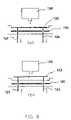
- FIGS. 1 a – 1 cshow prior art sequential processing systems and method.
- FIGS. 2 a – 2 cshow different views of an embodiment of the present invention assembly line processing system.
- FIGS. 3 a – 3 dshow different embodiments of precursor distribution of a process station.
- FIGS. 4 a – 4 dshow different embodiments of a workpiece support.
- FIGS. 5 a – 5 dshow different embodiments of isolation stations.
- FIGS. 6 a – 6 bshow different views of an embodiment of the present invention assembly line processing system using sub-atmospheric pressure processing.
- FIG. 7shows an embodiment of the present invention assembly line processing system using a load-or-unload station.
- FIGS. 8 a – 8 bshow different views of an embodiment of the present invention assembly line processing system using workpiece lift.
- FIGS. 9 a – 9 eshow different embodiments of precursor delivery systems.
- FIG. 11shows an embodiments of various stations.
- FIGS. 1 a – 1 cshow prior art sequential processing systems and method.
- FIG. 1 ashows a single wafer sequential processing system such as the one used in ALD processing.
- a wafer 5 ais positioned on a wafer support 6 a inside a processing chamber 4 a .
- the processing chamberhas various inlets 1 a , 2 a , and 3 a .
- Inlet 1 ais for introducing the first precursor
- inlet 2 ais for introducing the second precursor
- inlet 3 ais for introducing purge gas (a non-reactive gas such as an inert gas like helium or argon).
- the chamberis processed under sub-atmospheric pressure with a vacuum pump system connected to the outlet 7 a .
- FIG. 1 ashows a single wafer sequential processing system such as the one used in ALD processing.
- a wafer 5 ais positioned on a wafer support 6 a inside a processing chamber 4 a .
- FIG. 1 bshows a multiple wafer (batch) sequential processing system.
- the major difference between the single wafer and multiple wafer systemsis the number of wafers that can be processed at one time.
- Multiple wafers 5 bare positioned on multiple wafer supports 6 b inside processing chamber 4 b .
- the processing chamber 4 bhas various inlets 1 b , 2 b , and 3 b for the first precursor, the second precursor, and the purge gas, together with a pumping outlet 7 b .
- FIG. 1 cshows a typical method of sequential processing using a prior art sequential processing system.
- the first precursorflows into the process chamber 4 a , 4 b and reacts on the wafer 5 a , 5 b .
- the first precursoris adsorbed on the wafer surface.
- the first precursoris deposited on the wafer surface.
- the purge gasthen is introduced to push the first precursor out.
- a pumping stepthen follows to ensure that all of the first precursor is evacuated.
- the second precursoris introduced, and reacts on the wafer surface.
- the second precursoris then evacuated and then the cycle can be repeated until a desired thickness of the film is achieved.
- the basic operation of the prior art sequential systemis the sequential introduction of the precursors.
- FIGS. 2 a – 2 cshow different views of an embodiment of the present invention assembly line processing system.
- FIGS. 2 a , 2 b and 2 cshow different views of the assembly line processing system.
- Multiple workpieces 10such as wafers, are positioned on a rotatable workpiece conveyor 11 .
- Two different process stations 16 and 17are coupled to the workpiece conveyor 11 to deliver various processes to the workpieces 10 .
- Process station 16further comprises a plasma generator 22 to provide energetic precursors.
- Two isolation stations 24 and 25are positioned between the process stations 16 and 17 to minimize the cross contamination between the precursors of process stations 16 and 17 .
- a heating station 26can provide heating energy to the workpiece, and a plasma station 27 can provide plasma energy to the workpiece.
- the systemfurther comprises a load-or-unload station 29 to transfer the workpieces in and out of the processing system.
- a load-or-unload station 29to transfer the workpieces in and out of the processing system.
- the multiple workpieces 10are also rotated and pass through the multiple stations: the process stations 16 , 17 , the heating station 26 , the plasma station 27 and the isolation stations 24 and 25 .
- FIG. 2 cshows a spread-out of the apparatus.
- the method of operation for the present invention assembly line processing systemis as follows.
- the first precursoris introduced to processing station 16 and the second precursor is introduced to processing station 17 .
- the operations of plasma station 2 and heating station 26are optional.
- the isolation stations 24 and 25operate to prevent mixing of the first precursor and the second precursor Conveyor 11 rotates and the workpieces 10 are processed sequentially, first by the first precursor from processing station 16 and then by the second precursor from processing station 17 .
- the basic operation of the present invention sequential systemis the rotation of the conveyor 11 .
- the precursor flowcan be continuous, and need not be sequential as in the prior art.
- FIGS. 3 a – 3 dshow different embodiments of precursor distributors of a processing station.
- the precursor distributoris a linear injector.
- the processing station 40provides precursor onto a workpiece 10 .
- the workpiece 10is positioned on a workpiece conveyor 11 with a embedded resistive heater 19 to heat the workpiece 10 to an elevated temperature.
- the precursor distributoris an oblong showerhead injector.
- the precursor distributor dieis a round hole injector.
- the precursor distributoris also a round hole injector, but delivered sideways from a processing station 46 .
- FIGS. 4 a – 4 dshow different embodiments of a workpiece support.
- FIG. 4 ashows the workpiece support forming a cavity to contain the workpiece 10 .
- the processing station 51provides precursor to the workpiece 10 .
- the workpiece 10is supported by the workpiece support 52 of the conveyor 53 .
- the conveyor 53has an embedded resistive heater 19 to heat the workpiece to an elevated temperature.
- FIG. 4 bshows the workpiece support 54 of the conveyor 55 having a flat surface.
- FIG. 4 cshows the workpiece support 56 of the conveyor 57 having a recessed surface so that the workpiece 10 is raised above the conveyor 57 .
- the workpiece support 56is larger than the workpiece 10 .
- FIG. 4 dshows the workpiece support 58 of the conveyor 59 having a recessed surface so that the workpiece 10 is raised above the conveyor 57 .
- the workpiece support 58is smaller than the workpiece 10 .
- FIGS. 5 a – 5 dshow different embodiments of isolation stations.
- FIG. 5 ashows a cross-section view of part of the apparatus.
- the multiple workpieces 10are positioned on the workpiece conveyor 11 with two processing stations 70 and 71 .
- the precursor from processing station 70flows onto the workpiece, and then is captured by the pumping system of isolation station 73 .
- the precursor from processing station 71flows onto the workpiece, and then is captured by the pumping system of isolation station 75 .
- the purging system of isolation station 74creates a gas curtain to prevent cross flow of precursors from processing stations 70 and 71 .
- FIG. 5 bis a top view of the isolation station.
- the precursor distributors of processing stations 70 a and 71 aare linear injectors to the workpiece 10 on the conveyor 11 .
- the purge system of isolation station 74 acreates a gas flow toward the both the pumping systems of the isolation stations 73 a and 75 a to prevent the precursor from processing station 70 a from reacting with the precursor from processing station 71 a .
- FIG. 5 cis another embodiment of the isolation station where the pumping systems of isolation stations 73 b and 75 b cover completely processing stations 70 a and 71 a .
- the purging system of isolation station 74 bkeeps the precursors from processing stations 70 a and 71 a apart.
- FIG. 5 dis another embodiment of the isolation station where the pumping systems of isolation stations 73 c and 75 c cover completely the processing stations 70 c and 71 c .
- Conveyor 11 in FIG. 5 dis a rotatable platform, and can carry six workpieces 10 .
- the purging system of isolation station 74 ckeeps the precursors from processing stations 70 c and 71 c apart.
- FIGS. 6 a – 6 bshow different views of an embodiment of the present invention assembly line processing system using sub-atmospheric pressure processing.
- the rotatable conveyor 80can carry six workpieces 10 which can be arranged in a circle. There are two process stations 81 and 82 to provide precursors to the workpieces 10 .
- the pumping systems of the isolation stations 83 , 83 a , 83 b , 85 , 85 a , and 85 bcover completely processing stations 81 and 82 .
- the purging system of isolation station 84creates a gas curtain to further separate the precursors from processing stations 81 and 82 .
- the systemfurther comprises a lower section 87 to maintain sub-atmospheric pressure inside the chamber.
- the conveyor 80also has multiple heaters 88 embedded to the workpiece support to heat the workpieces 10 .
- the conveyor 80is rotatable and has a sealable rotatable bearing 89 (such as a ferrofluidic seal).
- FIG. 7shows an embodiment of the present invention assembly line processing system using a load-or-unload station.
- the load-or-unload stationcomprises a transfer arm 104 in a transfer housing 102 .
- the transfer arm 104can load or unload a workpiece 100 from the process chamber to the transfer housing 102 through an opening 112 in the transfer housing 102 .
- the workpiece 100then can be loaded or unloaded to a storage 108 through an opening 110 of the storage 108 .
- the storage 108can store a number 106 of workpieces 100 .
- FIGS. 8 a – 8 bshow different views of an embodiment of the present invention assembly line processing system using workpiece lifts.
- FIG. 8 ashows the workpiece 122 in processing station 128 while the processing station 128 is delivering a precursor to the workpiece 122 .
- the embedded heater 126 to heat the workpiece 122comprises multiple openings for the insertion of the workpiece lifts 124 .
- FIG. 8 bshows workpiece 120 in the up position, ready to be unloaded to the storage.
- the workpiece lifts 123are in up position, which raises the workpiece 120 up.
- the process station 128is not operational when the workpiece lifts 123 are in the up position and the workpiece 120 is raised, since the workpiece 120 is ready to be unloaded.
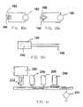
- FIGS. 9 a – 9 eshow different embodiments of precursor delivery systems.
- FIG. 9 ashows a gaseous precursor delivery system.
- the gaseous precursor 142is delivered through the metering device 140 to the workpiece.
- the heater 141is used to keep the gaseous precursor at a desired temperature. Typically, the gaseous precursor 142 is kept at a high pressure.
- FIG. 9 bshows a vapor draw liquid precursor delivery system.
- the precursoris in equilibrium in liquid form 146 and in vapor form 148 .
- the vapor form 148is drawn to a metering device 144 to the workpiece.
- a first heater 145heats the liquid precursor 146 to raise the partial pressure of the precursor vapor 148 .
- FIG. 9 cshows a bubbler liquid delivery system.
- the precursoris in equilibrium in liquid form 151 and in vapor form 154 .
- a carrier gas 153is bubbled through the liquid precursor 151 and carries the precursor vapor 154 through a metering device 149 to the workpiece.
- a first heater 152heats the liquid precursor 151 to raise the partial pressure of the precursor vapor 154 .
- a second heater 150prevents condensation of the vapor in the delivery line.
- FIG. 9 dshows a vapor draw solid precursor delivery system.
- the precursoris in equilibrium in solid form 157 and in vapor form 159 .
- the vapor form 159is drawn to a metering device 155 and to the workpiece.
- a first heater 158heats the solid precursor 157 to raise the partial pressure of the precursor vapor 159 .
- a second heater 156prevents condensation of the vapor in the delivery line.
- FIG. 9 eshows a liquid injection delivery system.
- a non-reactive gas 164exerts pressure 163 on the liquid precursor 162 to push the liquid precursor to a metering device 161 .
- the liquid precursor 165then travels to a vaporizer 168 to be converted to vapor form 166 .
- a heater 167heats the vaporizer to supply energy to the liquid precursor to convert to vapor form.
- FIGS. 10 a – 10 cshow different embodiments of plasma generators.
- FIG. 10 ashows a parallel plate plasma generator.
- a power source 180supplies power to a pair of parallel plates 182 , generates a high electric field between the parallel plates 182 , and excites the gas between the parallel plates 182 to generate a plasma 184 .
- This plasma 184is highly directional because of the electric field, and has a low density.
- FIG. 10 bshows an ICP.
- a power source 186supplies power to an inductive coil 188 , generates a high magnetic field inside the coil 188 , and excites the gas inside the coil 188 to generate a plasma 190 .
- This plasmais not directional and has a high ion density.
- FIG. 10 ashows a parallel plate plasma generator.
- a power source 180supplies power to a pair of parallel plates 182 , generates a high electric field between the parallel plates 182 , and excites the gas between the parallel plates 182 to
- the plasma generator 194generates a plasma 192 upstream of the flow and carries the excited and energetic species downstream 196 .
- This plasmahas little kinetic energy and a fairly uniform distribution of energy.
- Plasmacan be generated by a power source with RF (RF) such as a parallel plate plasma, remote plasma, or microwave frequency (“MW”) such as a remote plasma or a microwave plasma.
- RFRF
- MWmicrowave frequency
- FIG. 11shows an embodiments of various stations.
- the first stationis a plasma process station 202 .
- the processing station 202has a plasma generator 200 to excite the precursor before deliver to the workpiece.
- the second stationis a heating station 204 .
- the heating station 204delivers thermal energy and photon energy to the workpiece for heating and for reaction acceleration.
- the third stationis a laser station 206 .
- the laser station 206delivers laser energy to the workpiece for heating and for reaction acceleration.
- the fourth stationis a plasma station 208 .
- the plasma station 208delivers plasma energy to the workpiece.
- a bias source 210is also shown for biasing the workpiece for directional control of the charged species.
Landscapes
- Engineering & Computer Science (AREA)
- Chemical & Material Sciences (AREA)
- Manufacturing & Machinery (AREA)
- General Physics & Mathematics (AREA)
- Physics & Mathematics (AREA)
- Computer Hardware Design (AREA)
- Microelectronics & Electronic Packaging (AREA)
- Power Engineering (AREA)
- Condensed Matter Physics & Semiconductors (AREA)
- General Chemical & Material Sciences (AREA)
- Chemical Kinetics & Catalysis (AREA)
- Materials Engineering (AREA)
- Mechanical Engineering (AREA)
- Metallurgy (AREA)
- Organic Chemistry (AREA)
- Chemical Vapour Deposition (AREA)
Abstract
Description
- a) A number of workpieces are loaded onto the workpiece conveyor. The workpieces are positioned on the workpiece supports. There might be empty positions on the workpiece conveyor, e.g., each workpiece support does not necessarily have a workpiece.
- b) The first process station is turned on.
- c) The conveyor moves to process the workpieces under the first process station.
- d) When the workpieces, already processed under the first station, reach the second process station, the second process station is turned on. This operation offset of the second process station at the beginning of the process sequence ensures that all the workpieces have the same process sequence.
- e) The conveyor moves a number of cycles. The number of cycles determines the thickness of the thin film to be deposited.
- f) The first process station is turned off before the second process station. This operation offset of the first process station at the end of the process sequence ensures that all the workpieces have the same process sequence.
- g) The second process station is turned off.
- h) The conveyor stops and all the workpieces are unloaded from the conveyor.
- The workpieces positioned on the workpiece supports of the workpiece conveyor.
- The process stations operating continuously.
- The workpiece conveyor rotating continuously.
Claims (27)
Priority Applications (1)
| Application Number | Priority Date | Filing Date | Title |
|---|---|---|---|
| US10/212,546US7153542B2 (en) | 2002-08-06 | 2002-08-06 | Assembly line processing method |
Applications Claiming Priority (1)
| Application Number | Priority Date | Filing Date | Title |
|---|---|---|---|
| US10/212,546US7153542B2 (en) | 2002-08-06 | 2002-08-06 | Assembly line processing method |
Publications (2)
| Publication Number | Publication Date |
|---|---|
| US20040026374A1 US20040026374A1 (en) | 2004-02-12 |
| US7153542B2true US7153542B2 (en) | 2006-12-26 |
Family
ID=31494346
Family Applications (1)
| Application Number | Title | Priority Date | Filing Date |
|---|---|---|---|
| US10/212,546Expired - LifetimeUS7153542B2 (en) | 2002-08-06 | 2002-08-06 | Assembly line processing method |
Country Status (1)
| Country | Link |
|---|---|
| US (1) | US7153542B2 (en) |
Cited By (464)
| Publication number | Priority date | Publication date | Assignee | Title |
|---|---|---|---|---|
| US20060040055A1 (en)* | 2002-08-06 | 2006-02-23 | Tegal Corporation | Method and system for sequential processing in a two-compartment chamber |
| US20060046412A1 (en)* | 2002-08-06 | 2006-03-02 | Tegal Corporation | Method and system for sequential processing in a two-compartment chamber |
| US20070269609A1 (en)* | 2006-04-07 | 2007-11-22 | Linde Ag | Method And Apparatus For Radiation Curing |
| US20080133161A1 (en)* | 2005-10-11 | 2008-06-05 | Chiang Tony P | Methods for discretized processing and process sequence integration of regions of a substrate |
| US20080193643A1 (en)* | 2007-02-12 | 2008-08-14 | Tokyo Electron Limited | Atomic layer deposition systems and methods |
| US20090277871A1 (en)* | 2008-03-05 | 2009-11-12 | Axcelis Technologies, Inc. | Plasma mediated ashing processes that include formation of a protective layer before and/or during the plasma mediated ashing process |
| EP2138604A2 (en) | 2008-06-27 | 2009-12-30 | Tokyo Electron Limited | Film deposition apparatus, film deposition method, and computer readable storage medium |
| US20090324826A1 (en)* | 2008-06-27 | 2009-12-31 | Hitoshi Kato | Film Deposition Apparatus, Film Deposition Method, and Computer Readable Storage Medium |
| US20090324828A1 (en)* | 2008-06-27 | 2009-12-31 | Hitoshi Kato | Film deposition apparatus, film deposition method, and computer readable storage medium |
| US20100021720A1 (en)* | 2008-07-24 | 2010-01-28 | Shembel Elena M | Transparent coductive oxide and method of production thereof |
| US20100055312A1 (en)* | 2008-09-04 | 2010-03-04 | Tokyo Electron Limited | Film deposition apparatus, substrate processing apparatus, film deposition method, and computer-readable storage medium |
| US20100050944A1 (en)* | 2008-09-04 | 2010-03-04 | Tokyo Electron Limited | Film deposition apparatus, substrate process apparatus, and turntable |
| US20100055320A1 (en)* | 2008-09-04 | 2010-03-04 | Tokyo Electron Limited | Film deposition apparatus, substrate processing apparatus, film deposition method and storage medium |
| US20100050943A1 (en)* | 2008-09-04 | 2010-03-04 | Tokyo Electron Limited | Film deposition apparatus and substrate processing apparatus |
| US20100055314A1 (en)* | 2008-08-29 | 2010-03-04 | Tokyo Electron Limited | Film deposition apparatus, film deposition method, and storage medium |
| US20100055315A1 (en)* | 2008-09-04 | 2010-03-04 | Tokyo Electron Limited | Film deposition apparatus, substrate process apparatus, film deposition method, and computer readable storage medium |
| US20100055347A1 (en)* | 2008-08-29 | 2010-03-04 | Tokyo Electron Limited | Activated gas injector, film deposition apparatus, and film deposition method |
| US20100050942A1 (en)* | 2008-08-29 | 2010-03-04 | Tokyo Electron Limited | Film deposition apparatus and substrate process apparatus |
| US20100055319A1 (en)* | 2008-09-04 | 2010-03-04 | Tokyo Electron Limited | Film deposition apparatus, substrate processor, film deposition method, and computer-readable storage medium |
| US20100055317A1 (en)* | 2008-09-04 | 2010-03-04 | Tokyo Electron Limited | Film deposition apparatus exposing substrate to plural gases in sequence |
| US20100055297A1 (en)* | 2008-08-29 | 2010-03-04 | Tokyo Electron Limited | Film deposition apparatus, substrate processing apparatus, film deposition method, and computer-readable storage medium for film deposition method |
| US20100055316A1 (en)* | 2008-09-04 | 2010-03-04 | Tokyo Electron Limited | Film deposition apparatus, substrate processing apparatus, film deposition method, and storage medium |
| JP2010059497A (en)* | 2008-09-04 | 2010-03-18 | Tokyo Electron Ltd | Film deposition apparatus, film deposition method, program for making film deposition apparatus conduct the film deposition method and computer-readable storage medium for storing the program therein |
| US20100116209A1 (en)* | 2008-11-10 | 2010-05-13 | Tokyo Electron Limited | Film deposition apparatus |
| US20100116210A1 (en)* | 2008-11-10 | 2010-05-13 | Tokyo Electron Limited | Gas injector and film deposition apparatus |
| US20100132615A1 (en)* | 2008-12-02 | 2010-06-03 | Tokyo Electron Limited | Film deposition apparatus |
| US20100132614A1 (en)* | 2008-12-01 | 2010-06-03 | Tokyo Electron Limited | Film deposition apparatus |
| US20100151131A1 (en)* | 2008-12-12 | 2010-06-17 | Tokyo Electron Limited | Film deposition apparatus, film deposition method, and computer-readable storage medium |
| US20100227059A1 (en)* | 2009-03-04 | 2010-09-09 | Tokyo Electron Limited | Film deposition apparatus, film deposition method, and computer readable storage medium |
| US20100227046A1 (en)* | 2009-03-04 | 2010-09-09 | Tokyo Electron Limited | Film deposition apparatus, film deposition method, and computer readable storage medium |
| US20100260935A1 (en)* | 2009-04-09 | 2010-10-14 | Tokyo Electron Limited | Film deposition apparatus, film deposition method, and computer readable storage medium |
| US20100260936A1 (en)* | 2009-04-09 | 2010-10-14 | Tokyo Electron Limited | Substrate processing apparatus, substrate processing method, and computer-readable storage medium |
| US20100267191A1 (en)* | 2009-04-20 | 2010-10-21 | Applied Materials, Inc. | Plasma enhanced thermal evaporator |
| US20110039026A1 (en)* | 2009-08-11 | 2011-02-17 | Tokyo Electron Limited | Film deposition apparatus, film deposition method, and computer readable storage medium |
| US20110048326A1 (en)* | 2009-09-01 | 2011-03-03 | Tokyo Electron Limited | Film formation apparatus for semiconductor process |
| US20110100489A1 (en)* | 2009-11-04 | 2011-05-05 | Tokyo Electron Limited | Substrate process apparatus, substrate process method, and computer readable storage medium |
| US20110104395A1 (en)* | 2009-11-02 | 2011-05-05 | Tokyo Electron Limited | Film deposition apparatus, film deposition method, and storage medium |
| US20110126985A1 (en)* | 2009-12-02 | 2011-06-02 | Tokyo Electron Limited | Substrate processing apparatus |
| US20110139074A1 (en)* | 2009-12-10 | 2011-06-16 | Tokyo Electron Limited | Film deposition apparatus |
| US20110151122A1 (en)* | 2008-08-25 | 2011-06-23 | Tokyo Electron Limited | Film deposition apparatus, film deposition method, and computer readable storage medium |
| US20110159702A1 (en)* | 2009-12-25 | 2011-06-30 | Tokyo Electron Limited | Film deposition apparatus and film deposition method |
| US20110159188A1 (en)* | 2009-12-25 | 2011-06-30 | Tokyo Electron Limited | Film deposition apparatus, film deposition method, and computer-readable storage medium |
| US20110155057A1 (en)* | 2009-12-25 | 2011-06-30 | Tokyo Electron Limited | Plasma process apparatus |
| US20110214611A1 (en)* | 2008-11-14 | 2011-09-08 | Tokyo Electron Limited | Film deposition apparatus |
| US20110236598A1 (en)* | 2010-03-29 | 2011-09-29 | Tokyo Electron Limited | Film deposition apparatus, film deposition method, and computer readable storage medium |
| US20120220139A1 (en)* | 2009-10-14 | 2012-08-30 | Asm Japan K.K. | Method of depositing dielectric film by modified peald method |
| US20120266819A1 (en)* | 2011-04-25 | 2012-10-25 | Applied Materials, Inc. | Semiconductor substrate processing system |
| WO2012118955A3 (en)* | 2011-03-01 | 2012-11-15 | Applied Materials, Inc. | Apparatus and process for atomic layer deposition |
| US20130052346A1 (en)* | 2011-08-31 | 2013-02-28 | Alta Devices, Inc. | Cvd reactor with gas flow virtual walls |
| US20130133738A1 (en)* | 2010-06-10 | 2013-05-30 | Shin-Etsu Chemical Co., Ltd. | Firing furnace for firing electrode of solar cell element, method for manufacturing solar cell element, and solar cell element |
| US20130133580A1 (en)* | 2011-11-29 | 2013-05-30 | Intermolecular, Inc. | High productivity vapor processing system |
| US20130323422A1 (en)* | 2012-05-29 | 2013-12-05 | Applied Materials, Inc. | Apparatus for CVD and ALD with an Elongate Nozzle and Methods Of Use |
| US8636847B2 (en)* | 2008-12-04 | 2014-01-28 | Veeco Instruments Inc. | Chemical vapor deposition flow inlet elements and methods |
| US8944347B2 (en) | 2011-07-01 | 2015-02-03 | Industrial Technology Research Institute | Deposition nozzle and apparatus for thin film deposition process |
| DE102013219213A1 (en)* | 2013-09-24 | 2015-03-26 | Osram Gmbh | Process chamber for a chemical reaction coating process and method for coating an optical object by means of a chemical reaction coating process |
| US20150122876A1 (en)* | 2013-11-04 | 2015-05-07 | Solid State Equipment Llc | System and method for flux coat, reflow and clean |
| US9039837B2 (en) | 2011-07-21 | 2015-05-26 | Tokyo Electron Limited | Film deposition apparatus and substrate processing apparatus |
| KR20150064075A (en) | 2012-10-11 | 2015-06-10 | 도쿄엘렉트론가부시키가이샤 | Film-forming apparatus |
| US9111876B2 (en) | 2011-11-30 | 2015-08-18 | Applied Materials, Inc. | Methods for atomic layer etching |
| US9324811B2 (en) | 2012-09-26 | 2016-04-26 | Asm Ip Holding B.V. | Structures and devices including a tensile-stressed silicon arsenic layer and methods of forming same |
| US9384987B2 (en) | 2012-04-04 | 2016-07-05 | Asm Ip Holding B.V. | Metal oxide protective layer for a semiconductor device |
| US9394608B2 (en) | 2009-04-06 | 2016-07-19 | Asm America, Inc. | Semiconductor processing reactor and components thereof |
| US9404587B2 (en) | 2014-04-24 | 2016-08-02 | ASM IP Holding B.V | Lockout tagout for semiconductor vacuum valve |
| US9412564B2 (en) | 2013-07-22 | 2016-08-09 | Asm Ip Holding B.V. | Semiconductor reaction chamber with plasma capabilities |
| US9447498B2 (en) | 2014-03-18 | 2016-09-20 | Asm Ip Holding B.V. | Method for performing uniform processing in gas system-sharing multiple reaction chambers |
| US9449795B2 (en) | 2013-02-28 | 2016-09-20 | Novellus Systems, Inc. | Ceramic showerhead with embedded RF electrode for capacitively coupled plasma reactor |
| US9453280B2 (en) | 2011-09-05 | 2016-09-27 | Tokyo Electron Limited | Film deposition apparatus, film deposition method and storage medium |
| US9455138B1 (en) | 2015-11-10 | 2016-09-27 | Asm Ip Holding B.V. | Method for forming dielectric film in trenches by PEALD using H-containing gas |
| US9478415B2 (en) | 2015-02-13 | 2016-10-25 | Asm Ip Holding B.V. | Method for forming film having low resistance and shallow junction depth |
| US9484191B2 (en) | 2013-03-08 | 2016-11-01 | Asm Ip Holding B.V. | Pulsed remote plasma method and system |
| US9484233B2 (en) | 2012-04-13 | 2016-11-01 | Novellus Systems, Inc. | Carousel reactor for multi-station, sequential processing systems |
| US9543180B2 (en) | 2014-08-01 | 2017-01-10 | Asm Ip Holding B.V. | Apparatus and method for transporting wafers between wafer carrier and process tool under vacuum |
| US9556516B2 (en) | 2013-10-09 | 2017-01-31 | ASM IP Holding B.V | Method for forming Ti-containing film by PEALD using TDMAT or TDEAT |
| US9558931B2 (en) | 2012-07-27 | 2017-01-31 | Asm Ip Holding B.V. | System and method for gas-phase sulfur passivation of a semiconductor surface |
| US9583312B2 (en) | 2012-12-14 | 2017-02-28 | Tokyo Electron Limited | Film formation device, substrate processing device, and film formation method |
| US9589770B2 (en) | 2013-03-08 | 2017-03-07 | Asm Ip Holding B.V. | Method and systems for in-situ formation of intermediate reactive species |
| US9605342B2 (en) | 2012-09-12 | 2017-03-28 | Asm Ip Holding B.V. | Process gas management for an inductively-coupled plasma deposition reactor |
| US9607837B1 (en) | 2015-12-21 | 2017-03-28 | Asm Ip Holding B.V. | Method for forming silicon oxide cap layer for solid state diffusion process |
| US9627221B1 (en) | 2015-12-28 | 2017-04-18 | Asm Ip Holding B.V. | Continuous process incorporating atomic layer etching |
| US9640416B2 (en) | 2012-12-26 | 2017-05-02 | Asm Ip Holding B.V. | Single-and dual-chamber module-attachable wafer-handling chamber |
| US9647114B2 (en) | 2015-08-14 | 2017-05-09 | Asm Ip Holding B.V. | Methods of forming highly p-type doped germanium tin films and structures and devices including the films |
| US9657845B2 (en) | 2014-10-07 | 2017-05-23 | Asm Ip Holding B.V. | Variable conductance gas distribution apparatus and method |
| US9659799B2 (en) | 2012-08-28 | 2017-05-23 | Asm Ip Holding B.V. | Systems and methods for dynamic semiconductor process scheduling |
| US9711345B2 (en) | 2015-08-25 | 2017-07-18 | Asm Ip Holding B.V. | Method for forming aluminum nitride-based film by PEALD |
| US9714467B2 (en) | 2014-02-10 | 2017-07-25 | Tokyo Electron Limited | Method for processing a substrate and substrate processing apparatus |
| US9735024B2 (en) | 2015-12-28 | 2017-08-15 | Asm Ip Holding B.V. | Method of atomic layer etching using functional group-containing fluorocarbon |
| US9754779B1 (en) | 2016-02-19 | 2017-09-05 | Asm Ip Holding B.V. | Method for forming silicon nitride film selectively on sidewalls or flat surfaces of trenches |
| US9793135B1 (en) | 2016-07-14 | 2017-10-17 | ASM IP Holding B.V | Method of cyclic dry etching using etchant film |
| US9793148B2 (en) | 2011-06-22 | 2017-10-17 | Asm Japan K.K. | Method for positioning wafers in multiple wafer transport |
| US9790595B2 (en) | 2013-07-12 | 2017-10-17 | Asm Ip Holding B.V. | Method and system to reduce outgassing in a reaction chamber |
| US9793115B2 (en) | 2013-08-14 | 2017-10-17 | Asm Ip Holding B.V. | Structures and devices including germanium-tin films and methods of forming same |
| US9812320B1 (en) | 2016-07-28 | 2017-11-07 | Asm Ip Holding B.V. | Method and apparatus for filling a gap |
| US9859151B1 (en) | 2016-07-08 | 2018-01-02 | Asm Ip Holding B.V. | Selective film deposition method to form air gaps |
| US9887082B1 (en) | 2016-07-28 | 2018-02-06 | Asm Ip Holding B.V. | Method and apparatus for filling a gap |
| US9890456B2 (en) | 2014-08-21 | 2018-02-13 | Asm Ip Holding B.V. | Method and system for in situ formation of gas-phase compounds |
| US9891521B2 (en) | 2014-11-19 | 2018-02-13 | Asm Ip Holding B.V. | Method for depositing thin film |
| US9892908B2 (en) | 2011-10-28 | 2018-02-13 | Asm America, Inc. | Process feed management for semiconductor substrate processing |
| US9899405B2 (en) | 2014-12-22 | 2018-02-20 | Asm Ip Holding B.V. | Semiconductor device and manufacturing method thereof |
| US9899291B2 (en) | 2015-07-13 | 2018-02-20 | Asm Ip Holding B.V. | Method for protecting layer by forming hydrocarbon-based extremely thin film |
| US9905420B2 (en) | 2015-12-01 | 2018-02-27 | Asm Ip Holding B.V. | Methods of forming silicon germanium tin films and structures and devices including the films |
| US9909214B2 (en) | 2015-10-15 | 2018-03-06 | Asm Ip Holding B.V. | Method for depositing dielectric film in trenches by PEALD |
| US9916980B1 (en) | 2016-12-15 | 2018-03-13 | Asm Ip Holding B.V. | Method of forming a structure on a substrate |
| US9932674B2 (en) | 2011-05-12 | 2018-04-03 | Tokyo Electron Limited | Film deposition apparatus, film deposition method, and computer-readable recording medium |
| US9960072B2 (en) | 2015-09-29 | 2018-05-01 | Asm Ip Holding B.V. | Variable adjustment for precise matching of multiple chamber cavity housings |
| US9963782B2 (en)* | 2015-02-12 | 2018-05-08 | Asm Ip Holding B.V. | Semiconductor manufacturing apparatus |
| US10032628B2 (en) | 2016-05-02 | 2018-07-24 | Asm Ip Holding B.V. | Source/drain performance through conformal solid state doping |
| US10043661B2 (en) | 2015-07-13 | 2018-08-07 | Asm Ip Holding B.V. | Method for protecting layer by forming hydrocarbon-based extremely thin film |
| US10066297B2 (en) | 2011-08-31 | 2018-09-04 | Alta Devices, Inc. | Tiled showerhead for a semiconductor chemical vapor deposition reactor |
| US10083836B2 (en) | 2015-07-24 | 2018-09-25 | Asm Ip Holding B.V. | Formation of boron-doped titanium metal films with high work function |
| US10087525B2 (en) | 2015-08-04 | 2018-10-02 | Asm Ip Holding B.V. | Variable gap hard stop design |
| US10090316B2 (en) | 2016-09-01 | 2018-10-02 | Asm Ip Holding B.V. | 3D stacked multilayer semiconductor memory using doped select transistor channel |
| US10087522B2 (en) | 2016-04-21 | 2018-10-02 | Asm Ip Holding B.V. | Deposition of metal borides |
| US10103040B1 (en) | 2017-03-31 | 2018-10-16 | Asm Ip Holding B.V. | Apparatus and method for manufacturing a semiconductor device |
| USD830981S1 (en) | 2017-04-07 | 2018-10-16 | Asm Ip Holding B.V. | Susceptor for semiconductor substrate processing apparatus |
| US10134757B2 (en) | 2016-11-07 | 2018-11-20 | Asm Ip Holding B.V. | Method of processing a substrate and a device manufactured by using the method |
| US10167557B2 (en) | 2014-03-18 | 2019-01-01 | Asm Ip Holding B.V. | Gas distribution system, reactor including the system, and methods of using the same |
| US10177025B2 (en) | 2016-07-28 | 2019-01-08 | Asm Ip Holding B.V. | Method and apparatus for filling a gap |
| US10179947B2 (en) | 2013-11-26 | 2019-01-15 | Asm Ip Holding B.V. | Method for forming conformal nitrided, oxidized, or carbonized dielectric film by atomic layer deposition |
| US10190213B2 (en) | 2016-04-21 | 2019-01-29 | Asm Ip Holding B.V. | Deposition of metal borides |
| US10211308B2 (en) | 2015-10-21 | 2019-02-19 | Asm Ip Holding B.V. | NbMC layers |
| US10224182B2 (en) | 2011-10-17 | 2019-03-05 | Novellus Systems, Inc. | Mechanical suppression of parasitic plasma in substrate processing chamber |
| US10229833B2 (en) | 2016-11-01 | 2019-03-12 | Asm Ip Holding B.V. | Methods for forming a transition metal nitride film on a substrate by atomic layer deposition and related semiconductor device structures |
| US10236177B1 (en) | 2017-08-22 | 2019-03-19 | ASM IP Holding B.V.. | Methods for depositing a doped germanium tin semiconductor and related semiconductor device structures |
| US10249577B2 (en) | 2016-05-17 | 2019-04-02 | Asm Ip Holding B.V. | Method of forming metal interconnection and method of fabricating semiconductor apparatus using the method |
| US10249524B2 (en) | 2017-08-09 | 2019-04-02 | Asm Ip Holding B.V. | Cassette holder assembly for a substrate cassette and holding member for use in such assembly |
| US10262859B2 (en) | 2016-03-24 | 2019-04-16 | Asm Ip Holding B.V. | Process for forming a film on a substrate using multi-port injection assemblies |
| US10269558B2 (en) | 2016-12-22 | 2019-04-23 | Asm Ip Holding B.V. | Method of forming a structure on a substrate |
| US10276355B2 (en) | 2015-03-12 | 2019-04-30 | Asm Ip Holding B.V. | Multi-zone reactor, system including the reactor, and method of using the same |
| US10283353B2 (en) | 2017-03-29 | 2019-05-07 | Asm Ip Holding B.V. | Method of reforming insulating film deposited on substrate with recess pattern |
| US10290508B1 (en) | 2017-12-05 | 2019-05-14 | Asm Ip Holding B.V. | Method for forming vertical spacers for spacer-defined patterning |
| US10312055B2 (en) | 2017-07-26 | 2019-06-04 | Asm Ip Holding B.V. | Method of depositing film by PEALD using negative bias |
| US10319588B2 (en) | 2017-10-10 | 2019-06-11 | Asm Ip Holding B.V. | Method for depositing a metal chalcogenide on a substrate by cyclical deposition |
| US10322384B2 (en) | 2015-11-09 | 2019-06-18 | Asm Ip Holding B.V. | Counter flow mixer for process chamber |
| US10340135B2 (en) | 2016-11-28 | 2019-07-02 | Asm Ip Holding B.V. | Method of topologically restricted plasma-enhanced cyclic deposition of silicon or metal nitride |
| US10343920B2 (en) | 2016-03-18 | 2019-07-09 | Asm Ip Holding B.V. | Aligned carbon nanotubes |
| US10361201B2 (en) | 2013-09-27 | 2019-07-23 | Asm Ip Holding B.V. | Semiconductor structure and device formed using selective epitaxial process |
| US10367080B2 (en) | 2016-05-02 | 2019-07-30 | Asm Ip Holding B.V. | Method of forming a germanium oxynitride film |
| US10364496B2 (en) | 2011-06-27 | 2019-07-30 | Asm Ip Holding B.V. | Dual section module having shared and unshared mass flow controllers |
| US10378106B2 (en) | 2008-11-14 | 2019-08-13 | Asm Ip Holding B.V. | Method of forming insulation film by modified PEALD |
| US10381219B1 (en) | 2018-10-25 | 2019-08-13 | Asm Ip Holding B.V. | Methods for forming a silicon nitride film |
| US10381226B2 (en) | 2016-07-27 | 2019-08-13 | Asm Ip Holding B.V. | Method of processing substrate |
| US10388509B2 (en) | 2016-06-28 | 2019-08-20 | Asm Ip Holding B.V. | Formation of epitaxial layers via dislocation filtering |
| US10388513B1 (en) | 2018-07-03 | 2019-08-20 | Asm Ip Holding B.V. | Method for depositing silicon-free carbon-containing film as gap-fill layer by pulse plasma-assisted deposition |
| US10395919B2 (en) | 2016-07-28 | 2019-08-27 | Asm Ip Holding B.V. | Method and apparatus for filling a gap |
| US10403504B2 (en) | 2017-10-05 | 2019-09-03 | Asm Ip Holding B.V. | Method for selectively depositing a metallic film on a substrate |
| US10410943B2 (en) | 2016-10-13 | 2019-09-10 | Asm Ip Holding B.V. | Method for passivating a surface of a semiconductor and related systems |
| US10435790B2 (en) | 2016-11-01 | 2019-10-08 | Asm Ip Holding B.V. | Method of subatmospheric plasma-enhanced ALD using capacitively coupled electrodes with narrow gap |
| US10446393B2 (en) | 2017-05-08 | 2019-10-15 | Asm Ip Holding B.V. | Methods for forming silicon-containing epitaxial layers and related semiconductor device structures |
| US10458018B2 (en) | 2015-06-26 | 2019-10-29 | Asm Ip Holding B.V. | Structures including metal carbide material, devices including the structures, and methods of forming same |
| US10468261B2 (en) | 2017-02-15 | 2019-11-05 | Asm Ip Holding B.V. | Methods for forming a metallic film on a substrate by cyclical deposition and related semiconductor device structures |
| US10468251B2 (en) | 2016-02-19 | 2019-11-05 | Asm Ip Holding B.V. | Method for forming spacers using silicon nitride film for spacer-defined multiple patterning |
| US10480073B2 (en) | 2013-04-07 | 2019-11-19 | Shigemi Murakawa | Rotating semi-batch ALD device |
| US10483099B1 (en) | 2018-07-26 | 2019-11-19 | Asm Ip Holding B.V. | Method for forming thermally stable organosilicon polymer film |
| US10480067B2 (en) | 2016-02-03 | 2019-11-19 | Tokyo Electron Limited | Film deposition method |
| US10501866B2 (en) | 2016-03-09 | 2019-12-10 | Asm Ip Holding B.V. | Gas distribution apparatus for improved film uniformity in an epitaxial system |
| US10504742B2 (en) | 2017-05-31 | 2019-12-10 | Asm Ip Holding B.V. | Method of atomic layer etching using hydrogen plasma |
| US10510536B2 (en) | 2018-03-29 | 2019-12-17 | Asm Ip Holding B.V. | Method of depositing a co-doped polysilicon film on a surface of a substrate within a reaction chamber |
| US10529542B2 (en) | 2015-03-11 | 2020-01-07 | Asm Ip Holdings B.V. | Cross-flow reactor and method |
| US10529554B2 (en) | 2016-02-19 | 2020-01-07 | Asm Ip Holding B.V. | Method for forming silicon nitride film selectively on sidewalls or flat surfaces of trenches |
| US10529563B2 (en) | 2017-03-29 | 2020-01-07 | Asm Ip Holdings B.V. | Method for forming doped metal oxide films on a substrate by cyclical deposition and related semiconductor device structures |
| US10535516B2 (en) | 2018-02-01 | 2020-01-14 | Asm Ip Holdings B.V. | Method for depositing a semiconductor structure on a surface of a substrate and related semiconductor structures |
| US10541333B2 (en) | 2017-07-19 | 2020-01-21 | Asm Ip Holding B.V. | Method for depositing a group IV semiconductor and related semiconductor device structures |
| US10559458B1 (en) | 2018-11-26 | 2020-02-11 | Asm Ip Holding B.V. | Method of forming oxynitride film |
| US10590535B2 (en) | 2017-07-26 | 2020-03-17 | Asm Ip Holdings B.V. | Chemical treatment, deposition and/or infiltration apparatus and method for using the same |
| US10600673B2 (en) | 2015-07-07 | 2020-03-24 | Asm Ip Holding B.V. | Magnetic susceptor to baseplate seal |
| US10607895B2 (en) | 2017-09-18 | 2020-03-31 | Asm Ip Holdings B.V. | Method for forming a semiconductor device structure comprising a gate fill metal |
| US10605530B2 (en) | 2017-07-26 | 2020-03-31 | Asm Ip Holding B.V. | Assembly of a liner and a flange for a vertical furnace as well as the liner and the vertical furnace |
| USD880437S1 (en) | 2018-02-01 | 2020-04-07 | Asm Ip Holding B.V. | Gas supply plate for semiconductor manufacturing apparatus |
| US10612136B2 (en) | 2018-06-29 | 2020-04-07 | ASM IP Holding, B.V. | Temperature-controlled flange and reactor system including same |
| US10612137B2 (en) | 2016-07-08 | 2020-04-07 | Asm Ip Holdings B.V. | Organic reactants for atomic layer deposition |
| US10643904B2 (en) | 2016-11-01 | 2020-05-05 | Asm Ip Holdings B.V. | Methods for forming a semiconductor device and related semiconductor device structures |
| US10643826B2 (en) | 2016-10-26 | 2020-05-05 | Asm Ip Holdings B.V. | Methods for thermally calibrating reaction chambers |
| US10658181B2 (en) | 2018-02-20 | 2020-05-19 | Asm Ip Holding B.V. | Method of spacer-defined direct patterning in semiconductor fabrication |
| US10658205B2 (en) | 2017-09-28 | 2020-05-19 | Asm Ip Holdings B.V. | Chemical dispensing apparatus and methods for dispensing a chemical to a reaction chamber |
| US10655221B2 (en) | 2017-02-09 | 2020-05-19 | Asm Ip Holding B.V. | Method for depositing oxide film by thermal ALD and PEALD |
| US10685834B2 (en) | 2017-07-05 | 2020-06-16 | Asm Ip Holdings B.V. | Methods for forming a silicon germanium tin layer and related semiconductor device structures |
| US10683571B2 (en) | 2014-02-25 | 2020-06-16 | Asm Ip Holding B.V. | Gas supply manifold and method of supplying gases to chamber using same |
| US10692741B2 (en) | 2017-08-08 | 2020-06-23 | Asm Ip Holdings B.V. | Radiation shield |
| US10707106B2 (en) | 2011-06-06 | 2020-07-07 | Asm Ip Holding B.V. | High-throughput semiconductor-processing apparatus equipped with multiple dual-chamber modules |
| US10714315B2 (en) | 2012-10-12 | 2020-07-14 | Asm Ip Holdings B.V. | Semiconductor reaction chamber showerhead |
| US10714385B2 (en) | 2016-07-19 | 2020-07-14 | Asm Ip Holding B.V. | Selective deposition of tungsten |
| US10714350B2 (en) | 2016-11-01 | 2020-07-14 | ASM IP Holdings, B.V. | Methods for forming a transition metal niobium nitride film on a substrate by atomic layer deposition and related semiconductor device structures |
| US10714335B2 (en) | 2017-04-25 | 2020-07-14 | Asm Ip Holding B.V. | Method of depositing thin film and method of manufacturing semiconductor device |
| US10731249B2 (en) | 2018-02-15 | 2020-08-04 | Asm Ip Holding B.V. | Method of forming a transition metal containing film on a substrate by a cyclical deposition process, a method for supplying a transition metal halide compound to a reaction chamber, and related vapor deposition apparatus |
| US10734244B2 (en) | 2017-11-16 | 2020-08-04 | Asm Ip Holding B.V. | Method of processing a substrate and a device manufactured by the same |
| US10734497B2 (en) | 2017-07-18 | 2020-08-04 | Asm Ip Holding B.V. | Methods for forming a semiconductor device structure and related semiconductor device structures |
| US10755922B2 (en) | 2018-07-03 | 2020-08-25 | Asm Ip Holding B.V. | Method for depositing silicon-free carbon-containing film as gap-fill layer by pulse plasma-assisted deposition |
| US10770286B2 (en) | 2017-05-08 | 2020-09-08 | Asm Ip Holdings B.V. | Methods for selectively forming a silicon nitride film on a substrate and related semiconductor device structures |
| US10770336B2 (en) | 2017-08-08 | 2020-09-08 | Asm Ip Holding B.V. | Substrate lift mechanism and reactor including same |
| US10767789B2 (en) | 2018-07-16 | 2020-09-08 | Asm Ip Holding B.V. | Diaphragm valves, valve components, and methods for forming valve components |
| CN111670265A (en)* | 2018-01-31 | 2020-09-15 | 朗姆研究公司 | Manifold valve for multiple precursors |
| US10797133B2 (en) | 2018-06-21 | 2020-10-06 | Asm Ip Holding B.V. | Method for depositing a phosphorus doped silicon arsenide film and related semiconductor device structures |
| US10804098B2 (en) | 2009-08-14 | 2020-10-13 | Asm Ip Holding B.V. | Systems and methods for thin-film deposition of metal oxides using excited nitrogen-oxygen species |
| US10811256B2 (en) | 2018-10-16 | 2020-10-20 | Asm Ip Holding B.V. | Method for etching a carbon-containing feature |
| USD900036S1 (en) | 2017-08-24 | 2020-10-27 | Asm Ip Holding B.V. | Heater electrical connector and adapter |
| US10818758B2 (en) | 2018-11-16 | 2020-10-27 | Asm Ip Holding B.V. | Methods for forming a metal silicate film on a substrate in a reaction chamber and related semiconductor device structures |
| US10829852B2 (en) | 2018-08-16 | 2020-11-10 | Asm Ip Holding B.V. | Gas distribution device for a wafer processing apparatus |
| US10844484B2 (en) | 2017-09-22 | 2020-11-24 | Asm Ip Holding B.V. | Apparatus for dispensing a vapor phase reactant to a reaction chamber and related methods |
| US10847365B2 (en) | 2018-10-11 | 2020-11-24 | Asm Ip Holding B.V. | Method of forming conformal silicon carbide film by cyclic CVD |
| US10847371B2 (en) | 2018-03-27 | 2020-11-24 | Asm Ip Holding B.V. | Method of forming an electrode on a substrate and a semiconductor device structure including an electrode |
| US10847366B2 (en) | 2018-11-16 | 2020-11-24 | Asm Ip Holding B.V. | Methods for depositing a transition metal chalcogenide film on a substrate by a cyclical deposition process |
| US10854498B2 (en) | 2011-07-15 | 2020-12-01 | Asm Ip Holding B.V. | Wafer-supporting device and method for producing same |
| USD903477S1 (en) | 2018-01-24 | 2020-12-01 | Asm Ip Holdings B.V. | Metal clamp |
| US10858737B2 (en) | 2014-07-28 | 2020-12-08 | Asm Ip Holding B.V. | Showerhead assembly and components thereof |
| US10867786B2 (en) | 2018-03-30 | 2020-12-15 | Asm Ip Holding B.V. | Substrate processing method |
| US10867788B2 (en) | 2016-12-28 | 2020-12-15 | Asm Ip Holding B.V. | Method of forming a structure on a substrate |
| US10865475B2 (en) | 2016-04-21 | 2020-12-15 | Asm Ip Holding B.V. | Deposition of metal borides and silicides |
| US10872771B2 (en) | 2018-01-16 | 2020-12-22 | Asm Ip Holding B. V. | Method for depositing a material film on a substrate within a reaction chamber by a cyclical deposition process and related device structures |
| US10883175B2 (en) | 2018-08-09 | 2021-01-05 | Asm Ip Holding B.V. | Vertical furnace for processing substrates and a liner for use therein |
| US10886123B2 (en) | 2017-06-02 | 2021-01-05 | Asm Ip Holding B.V. | Methods for forming low temperature semiconductor layers and related semiconductor device structures |
| US10892156B2 (en) | 2017-05-08 | 2021-01-12 | Asm Ip Holding B.V. | Methods for forming a silicon nitride film on a substrate and related semiconductor device structures |
| US10896820B2 (en) | 2018-02-14 | 2021-01-19 | Asm Ip Holding B.V. | Method for depositing a ruthenium-containing film on a substrate by a cyclical deposition process |
| US10900121B2 (en) | 2016-11-21 | 2021-01-26 | Tokyo Electron Limited | Method of manufacturing semiconductor device and apparatus of manufacturing semiconductor device |
| US10910262B2 (en) | 2017-11-16 | 2021-02-02 | Asm Ip Holding B.V. | Method of selectively depositing a capping layer structure on a semiconductor device structure |
| US10914004B2 (en) | 2018-06-29 | 2021-02-09 | Asm Ip Holding B.V. | Thin-film deposition method and manufacturing method of semiconductor device |
| US10923344B2 (en) | 2017-10-30 | 2021-02-16 | Asm Ip Holding B.V. | Methods for forming a semiconductor structure and related semiconductor structures |
| US10928731B2 (en) | 2017-09-21 | 2021-02-23 | Asm Ip Holding B.V. | Method of sequential infiltration synthesis treatment of infiltrateable material and structures and devices formed using same |
| US10934619B2 (en) | 2016-11-15 | 2021-03-02 | Asm Ip Holding B.V. | Gas supply unit and substrate processing apparatus including the gas supply unit |
| US10941490B2 (en) | 2014-10-07 | 2021-03-09 | Asm Ip Holding B.V. | Multiple temperature range susceptor, assembly, reactor and system including the susceptor, and methods of using the same |
| US10975470B2 (en) | 2018-02-23 | 2021-04-13 | Asm Ip Holding B.V. | Apparatus for detecting or monitoring for a chemical precursor in a high temperature environment |
| US11001925B2 (en) | 2016-12-19 | 2021-05-11 | Asm Ip Holding B.V. | Substrate processing apparatus |
| US11018047B2 (en) | 2018-01-25 | 2021-05-25 | Asm Ip Holding B.V. | Hybrid lift pin |
| US11015245B2 (en) | 2014-03-19 | 2021-05-25 | Asm Ip Holding B.V. | Gas-phase reactor and system having exhaust plenum and components thereof |
| US11018002B2 (en) | 2017-07-19 | 2021-05-25 | Asm Ip Holding B.V. | Method for selectively depositing a Group IV semiconductor and related semiconductor device structures |
| US11024523B2 (en) | 2018-09-11 | 2021-06-01 | Asm Ip Holding B.V. | Substrate processing apparatus and method |
| US11022879B2 (en) | 2017-11-24 | 2021-06-01 | Asm Ip Holding B.V. | Method of forming an enhanced unexposed photoresist layer |
| US11031242B2 (en) | 2018-11-07 | 2021-06-08 | Asm Ip Holding B.V. | Methods for depositing a boron doped silicon germanium film |
| USD922229S1 (en) | 2019-06-05 | 2021-06-15 | Asm Ip Holding B.V. | Device for controlling a temperature of a gas supply unit |
| US11049751B2 (en) | 2018-09-14 | 2021-06-29 | Asm Ip Holding B.V. | Cassette supply system to store and handle cassettes and processing apparatus equipped therewith |
| US11053591B2 (en) | 2018-08-06 | 2021-07-06 | Asm Ip Holding B.V. | Multi-port gas injection system and reactor system including same |
| US11056344B2 (en) | 2017-08-30 | 2021-07-06 | Asm Ip Holding B.V. | Layer forming method |
| US11056567B2 (en) | 2018-05-11 | 2021-07-06 | Asm Ip Holding B.V. | Method of forming a doped metal carbide film on a substrate and related semiconductor device structures |
| US11069510B2 (en) | 2017-08-30 | 2021-07-20 | Asm Ip Holding B.V. | Substrate processing apparatus |
| US11081345B2 (en) | 2018-02-06 | 2021-08-03 | Asm Ip Holding B.V. | Method of post-deposition treatment for silicon oxide film |
| US11087997B2 (en) | 2018-10-31 | 2021-08-10 | Asm Ip Holding B.V. | Substrate processing apparatus for processing substrates |
| US11088002B2 (en) | 2018-03-29 | 2021-08-10 | Asm Ip Holding B.V. | Substrate rack and a substrate processing system and method |
| US11114294B2 (en) | 2019-03-08 | 2021-09-07 | Asm Ip Holding B.V. | Structure including SiOC layer and method of forming same |
| US11114283B2 (en) | 2018-03-16 | 2021-09-07 | Asm Ip Holding B.V. | Reactor, system including the reactor, and methods of manufacturing and using same |
| USD930782S1 (en) | 2019-08-22 | 2021-09-14 | Asm Ip Holding B.V. | Gas distributor |
| US11118265B2 (en) | 2010-08-27 | 2021-09-14 | Tokyo Electron Limited | Film deposition method and computer program storage medium |
| US11127589B2 (en) | 2019-02-01 | 2021-09-21 | Asm Ip Holding B.V. | Method of topology-selective film formation of silicon oxide |
| US11127617B2 (en) | 2017-11-27 | 2021-09-21 | Asm Ip Holding B.V. | Storage device for storing wafer cassettes for use with a batch furnace |
| USD931978S1 (en) | 2019-06-27 | 2021-09-28 | Asm Ip Holding B.V. | Showerhead vacuum transport |
| US11139308B2 (en) | 2015-12-29 | 2021-10-05 | Asm Ip Holding B.V. | Atomic layer deposition of III-V compounds to form V-NAND devices |
| US11139191B2 (en) | 2017-08-09 | 2021-10-05 | Asm Ip Holding B.V. | Storage apparatus for storing cassettes for substrates and processing apparatus equipped therewith |
| US11158513B2 (en) | 2018-12-13 | 2021-10-26 | Asm Ip Holding B.V. | Methods for forming a rhenium-containing film on a substrate by a cyclical deposition process and related semiconductor device structures |
| USD935572S1 (en) | 2019-05-24 | 2021-11-09 | Asm Ip Holding B.V. | Gas channel plate |
| US11171025B2 (en) | 2019-01-22 | 2021-11-09 | Asm Ip Holding B.V. | Substrate processing device |
| US11205585B2 (en) | 2016-07-28 | 2021-12-21 | Asm Ip Holding B.V. | Substrate processing apparatus and method of operating the same |
| US20210404061A1 (en)* | 2018-05-16 | 2021-12-30 | Applied Materials, Inc. | Atomic layer self aligned substrate processing and integrated toolset |
| US11217444B2 (en) | 2018-11-30 | 2022-01-04 | Asm Ip Holding B.V. | Method for forming an ultraviolet radiation responsive metal oxide-containing film |
| USD940837S1 (en) | 2019-08-22 | 2022-01-11 | Asm Ip Holding B.V. | Electrode |
| US11222772B2 (en) | 2016-12-14 | 2022-01-11 | Asm Ip Holding B.V. | Substrate processing apparatus |
| US11227789B2 (en) | 2019-02-20 | 2022-01-18 | Asm Ip Holding B.V. | Method and apparatus for filling a recess formed within a substrate surface |
| US11227782B2 (en) | 2019-07-31 | 2022-01-18 | Asm Ip Holding B.V. | Vertical batch furnace assembly |
| US11232963B2 (en) | 2018-10-03 | 2022-01-25 | Asm Ip Holding B.V. | Substrate processing apparatus and method |
| US11230766B2 (en) | 2018-03-29 | 2022-01-25 | Asm Ip Holding B.V. | Substrate processing apparatus and method |
| US11251040B2 (en) | 2019-02-20 | 2022-02-15 | Asm Ip Holding B.V. | Cyclical deposition method including treatment step and apparatus for same |
| US11251068B2 (en) | 2018-10-19 | 2022-02-15 | Asm Ip Holding B.V. | Substrate processing apparatus and substrate processing method |
| USD944946S1 (en) | 2019-06-14 | 2022-03-01 | Asm Ip Holding B.V. | Shower plate |
| US11270899B2 (en) | 2018-06-04 | 2022-03-08 | Asm Ip Holding B.V. | Wafer handling chamber with moisture reduction |
| US11274369B2 (en) | 2018-09-11 | 2022-03-15 | Asm Ip Holding B.V. | Thin film deposition method |
| US11282698B2 (en) | 2019-07-19 | 2022-03-22 | Asm Ip Holding B.V. | Method of forming topology-controlled amorphous carbon polymer film |
| US11286558B2 (en) | 2019-08-23 | 2022-03-29 | Asm Ip Holding B.V. | Methods for depositing a molybdenum nitride film on a surface of a substrate by a cyclical deposition process and related semiconductor device structures including a molybdenum nitride film |
| US11286562B2 (en) | 2018-06-08 | 2022-03-29 | Asm Ip Holding B.V. | Gas-phase chemical reactor and method of using same |
| US11289326B2 (en) | 2019-05-07 | 2022-03-29 | Asm Ip Holding B.V. | Method for reforming amorphous carbon polymer film |
| USD947913S1 (en) | 2019-05-17 | 2022-04-05 | Asm Ip Holding B.V. | Susceptor shaft |
| US11295980B2 (en) | 2017-08-30 | 2022-04-05 | Asm Ip Holding B.V. | Methods for depositing a molybdenum metal film over a dielectric surface of a substrate by a cyclical deposition process and related semiconductor device structures |
| USD948463S1 (en) | 2018-10-24 | 2022-04-12 | Asm Ip Holding B.V. | Susceptor for semiconductor substrate supporting apparatus |
| USD949319S1 (en) | 2019-08-22 | 2022-04-19 | Asm Ip Holding B.V. | Exhaust duct |
| US11306395B2 (en) | 2017-06-28 | 2022-04-19 | Asm Ip Holding B.V. | Methods for depositing a transition metal nitride film on a substrate by atomic layer deposition and related deposition apparatus |
| US11315794B2 (en) | 2019-10-21 | 2022-04-26 | Asm Ip Holding B.V. | Apparatus and methods for selectively etching films |
| US11342216B2 (en) | 2019-02-20 | 2022-05-24 | Asm Ip Holding B.V. | Cyclical deposition method and apparatus for filling a recess formed within a substrate surface |
| US11339476B2 (en) | 2019-10-08 | 2022-05-24 | Asm Ip Holding B.V. | Substrate processing device having connection plates, substrate processing method |
| US11345999B2 (en) | 2019-06-06 | 2022-05-31 | Asm Ip Holding B.V. | Method of using a gas-phase reactor system including analyzing exhausted gas |
| US11355338B2 (en) | 2019-05-10 | 2022-06-07 | Asm Ip Holding B.V. | Method of depositing material onto a surface and structure formed according to the method |
| US11361990B2 (en) | 2018-05-28 | 2022-06-14 | Asm Ip Holding B.V. | Substrate processing method and device manufactured by using the same |
| US20220186367A1 (en)* | 2020-12-13 | 2022-06-16 | Applied Materials, Inc. | Deposition Apparatus and Methods Using Staggered Pumping Locations |
| US11374112B2 (en) | 2017-07-19 | 2022-06-28 | Asm Ip Holding B.V. | Method for depositing a group IV semiconductor and related semiconductor device structures |
| US11378337B2 (en) | 2019-03-28 | 2022-07-05 | Asm Ip Holding B.V. | Door opener and substrate processing apparatus provided therewith |
| US11390945B2 (en) | 2019-07-03 | 2022-07-19 | Asm Ip Holding B.V. | Temperature control assembly for substrate processing apparatus and method of using same |
| US11390946B2 (en) | 2019-01-17 | 2022-07-19 | Asm Ip Holding B.V. | Methods of forming a transition metal containing film on a substrate by a cyclical deposition process |
| US11393690B2 (en) | 2018-01-19 | 2022-07-19 | Asm Ip Holding B.V. | Deposition method |
| US11390950B2 (en) | 2017-01-10 | 2022-07-19 | Asm Ip Holding B.V. | Reactor system and method to reduce residue buildup during a film deposition process |
| US11401605B2 (en) | 2019-11-26 | 2022-08-02 | Asm Ip Holding B.V. | Substrate processing apparatus |
| US11414760B2 (en) | 2018-10-08 | 2022-08-16 | Asm Ip Holding B.V. | Substrate support unit, thin film deposition apparatus including the same, and substrate processing apparatus including the same |
| US11424119B2 (en) | 2019-03-08 | 2022-08-23 | Asm Ip Holding B.V. | Method for selective deposition of silicon nitride layer and structure including selectively-deposited silicon nitride layer |
| US11430674B2 (en) | 2018-08-22 | 2022-08-30 | Asm Ip Holding B.V. | Sensor array, apparatus for dispensing a vapor phase reactant to a reaction chamber and related methods |
| US11430640B2 (en) | 2019-07-30 | 2022-08-30 | Asm Ip Holding B.V. | Substrate processing apparatus |
| US11437241B2 (en) | 2020-04-08 | 2022-09-06 | Asm Ip Holding B.V. | Apparatus and methods for selectively etching silicon oxide films |
| US11443926B2 (en) | 2019-07-30 | 2022-09-13 | Asm Ip Holding B.V. | Substrate processing apparatus |
| US11447861B2 (en) | 2016-12-15 | 2022-09-20 | Asm Ip Holding B.V. | Sequential infiltration synthesis apparatus and a method of forming a patterned structure |
| US11447864B2 (en) | 2019-04-19 | 2022-09-20 | Asm Ip Holding B.V. | Layer forming method and apparatus |
| USD965044S1 (en) | 2019-08-19 | 2022-09-27 | Asm Ip Holding B.V. | Susceptor shaft |
| US11453943B2 (en) | 2016-05-25 | 2022-09-27 | Asm Ip Holding B.V. | Method for forming carbon-containing silicon/metal oxide or nitride film by ALD using silicon precursor and hydrocarbon precursor |
| USD965524S1 (en) | 2019-08-19 | 2022-10-04 | Asm Ip Holding B.V. | Susceptor support |
| US11469098B2 (en) | 2018-05-08 | 2022-10-11 | Asm Ip Holding B.V. | Methods for depositing an oxide film on a substrate by a cyclical deposition process and related device structures |
| US11476109B2 (en) | 2019-06-11 | 2022-10-18 | Asm Ip Holding B.V. | Method of forming an electronic structure using reforming gas, system for performing the method, and structure formed using the method |
| US11473195B2 (en) | 2018-03-01 | 2022-10-18 | Asm Ip Holding B.V. | Semiconductor processing apparatus and a method for processing a substrate |
| US11482533B2 (en) | 2019-02-20 | 2022-10-25 | Asm Ip Holding B.V. | Apparatus and methods for plug fill deposition in 3-D NAND applications |
| US11482412B2 (en) | 2018-01-19 | 2022-10-25 | Asm Ip Holding B.V. | Method for depositing a gap-fill layer by plasma-assisted deposition |
| US11482418B2 (en) | 2018-02-20 | 2022-10-25 | Asm Ip Holding B.V. | Substrate processing method and apparatus |
| US11488854B2 (en) | 2020-03-11 | 2022-11-01 | Asm Ip Holding B.V. | Substrate handling device with adjustable joints |
| US11488819B2 (en) | 2018-12-04 | 2022-11-01 | Asm Ip Holding B.V. | Method of cleaning substrate processing apparatus |
| US11495459B2 (en) | 2019-09-04 | 2022-11-08 | Asm Ip Holding B.V. | Methods for selective deposition using a sacrificial capping layer |
| US11492703B2 (en) | 2018-06-27 | 2022-11-08 | Asm Ip Holding B.V. | Cyclic deposition methods for forming metal-containing material and films and structures including the metal-containing material |
| US11501968B2 (en) | 2019-11-15 | 2022-11-15 | Asm Ip Holding B.V. | Method for providing a semiconductor device with silicon filled gaps |
| US11499222B2 (en) | 2018-06-27 | 2022-11-15 | Asm Ip Holding B.V. | Cyclic deposition methods for forming metal-containing material and films and structures including the metal-containing material |
| US11499226B2 (en) | 2018-11-02 | 2022-11-15 | Asm Ip Holding B.V. | Substrate supporting unit and a substrate processing device including the same |
| US11515187B2 (en) | 2020-05-01 | 2022-11-29 | Asm Ip Holding B.V. | Fast FOUP swapping with a FOUP handler |
| US11515188B2 (en) | 2019-05-16 | 2022-11-29 | Asm Ip Holding B.V. | Wafer boat handling device, vertical batch furnace and method |
| US11521851B2 (en) | 2020-02-03 | 2022-12-06 | Asm Ip Holding B.V. | Method of forming structures including a vanadium or indium layer |
| US11527400B2 (en) | 2019-08-23 | 2022-12-13 | Asm Ip Holding B.V. | Method for depositing silicon oxide film having improved quality by peald using bis(diethylamino)silane |
| US11527403B2 (en) | 2019-12-19 | 2022-12-13 | Asm Ip Holding B.V. | Methods for filling a gap feature on a substrate surface and related semiconductor structures |
| US11530483B2 (en) | 2018-06-21 | 2022-12-20 | Asm Ip Holding B.V. | Substrate processing system |
| US11530876B2 (en) | 2020-04-24 | 2022-12-20 | Asm Ip Holding B.V. | Vertical batch furnace assembly comprising a cooling gas supply |
| US11532757B2 (en) | 2016-10-27 | 2022-12-20 | Asm Ip Holding B.V. | Deposition of charge trapping layers |
| US11551912B2 (en) | 2020-01-20 | 2023-01-10 | Asm Ip Holding B.V. | Method of forming thin film and method of modifying surface of thin film |
| US11551925B2 (en) | 2019-04-01 | 2023-01-10 | Asm Ip Holding B.V. | Method for manufacturing a semiconductor device |
| USD975665S1 (en) | 2019-05-17 | 2023-01-17 | Asm Ip Holding B.V. | Susceptor shaft |
| US11557474B2 (en) | 2019-07-29 | 2023-01-17 | Asm Ip Holding B.V. | Methods for selective deposition utilizing n-type dopants and/or alternative dopants to achieve high dopant incorporation |
| US11562901B2 (en) | 2019-09-25 | 2023-01-24 | Asm Ip Holding B.V. | Substrate processing method |
| US11572620B2 (en) | 2018-11-06 | 2023-02-07 | Asm Ip Holding B.V. | Methods for selectively depositing an amorphous silicon film on a substrate |
| US11581186B2 (en) | 2016-12-15 | 2023-02-14 | Asm Ip Holding B.V. | Sequential infiltration synthesis apparatus |
| US11587815B2 (en) | 2019-07-31 | 2023-02-21 | Asm Ip Holding B.V. | Vertical batch furnace assembly |
| US11587814B2 (en) | 2019-07-31 | 2023-02-21 | Asm Ip Holding B.V. | Vertical batch furnace assembly |
| US11594600B2 (en) | 2019-11-05 | 2023-02-28 | Asm Ip Holding B.V. | Structures with doped semiconductor layers and methods and systems for forming same |
| USD979506S1 (en) | 2019-08-22 | 2023-02-28 | Asm Ip Holding B.V. | Insulator |
| US11594450B2 (en) | 2019-08-22 | 2023-02-28 | Asm Ip Holding B.V. | Method for forming a structure with a hole |
| US11605528B2 (en) | 2019-07-09 | 2023-03-14 | Asm Ip Holding B.V. | Plasma device using coaxial waveguide, and substrate treatment method |
| USD980813S1 (en) | 2021-05-11 | 2023-03-14 | Asm Ip Holding B.V. | Gas flow control plate for substrate processing apparatus |
| USD980814S1 (en) | 2021-05-11 | 2023-03-14 | Asm Ip Holding B.V. | Gas distributor for substrate processing apparatus |
| US20230085140A1 (en)* | 2021-09-13 | 2023-03-16 | Kokusai Electric Corporation | Substrate processing apparatus, method of manufacturing semiconductor device, and non-transitory computer-readable recording medium |
| US11610774B2 (en) | 2019-10-02 | 2023-03-21 | Asm Ip Holding B.V. | Methods for forming a topographically selective silicon oxide film by a cyclical plasma-enhanced deposition process |
| USD981973S1 (en) | 2021-05-11 | 2023-03-28 | Asm Ip Holding B.V. | Reactor wall for substrate processing apparatus |
| US11615970B2 (en) | 2019-07-17 | 2023-03-28 | Asm Ip Holding B.V. | Radical assist ignition plasma system and method |
| US11626316B2 (en) | 2019-11-20 | 2023-04-11 | Asm Ip Holding B.V. | Method of depositing carbon-containing material on a surface of a substrate, structure formed using the method, and system for forming the structure |
| US11626308B2 (en) | 2020-05-13 | 2023-04-11 | Asm Ip Holding B.V. | Laser alignment fixture for a reactor system |
| US11629406B2 (en) | 2018-03-09 | 2023-04-18 | Asm Ip Holding B.V. | Semiconductor processing apparatus comprising one or more pyrometers for measuring a temperature of a substrate during transfer of the substrate |
| US11629407B2 (en) | 2019-02-22 | 2023-04-18 | Asm Ip Holding B.V. | Substrate processing apparatus and method for processing substrates |
| US11637011B2 (en) | 2019-10-16 | 2023-04-25 | Asm Ip Holding B.V. | Method of topology-selective film formation of silicon oxide |
| US11637014B2 (en) | 2019-10-17 | 2023-04-25 | Asm Ip Holding B.V. | Methods for selective deposition of doped semiconductor material |
| US11639548B2 (en) | 2019-08-21 | 2023-05-02 | Asm Ip Holding B.V. | Film-forming material mixed-gas forming device and film forming device |
| US11639811B2 (en) | 2017-11-27 | 2023-05-02 | Asm Ip Holding B.V. | Apparatus including a clean mini environment |
| US11644758B2 (en) | 2020-07-17 | 2023-05-09 | Asm Ip Holding B.V. | Structures and methods for use in photolithography |
| US11646204B2 (en) | 2020-06-24 | 2023-05-09 | Asm Ip Holding B.V. | Method for forming a layer provided with silicon |
| US11646205B2 (en) | 2019-10-29 | 2023-05-09 | Asm Ip Holding B.V. | Methods of selectively forming n-type doped material on a surface, systems for selectively forming n-type doped material, and structures formed using same |
| US11643724B2 (en) | 2019-07-18 | 2023-05-09 | Asm Ip Holding B.V. | Method of forming structures using a neutral beam |
| US11646184B2 (en) | 2019-11-29 | 2023-05-09 | Asm Ip Holding B.V. | Substrate processing apparatus |
| US11658029B2 (en) | 2018-12-14 | 2023-05-23 | Asm Ip Holding B.V. | Method of forming a device structure using selective deposition of gallium nitride and system for same |
| US11658035B2 (en) | 2020-06-30 | 2023-05-23 | Asm Ip Holding B.V. | Substrate processing method |
| US11664245B2 (en) | 2019-07-16 | 2023-05-30 | Asm Ip Holding B.V. | Substrate processing device |
| US11664199B2 (en) | 2018-10-19 | 2023-05-30 | Asm Ip Holding B.V. | Substrate processing apparatus and substrate processing method |
| US11664267B2 (en) | 2019-07-10 | 2023-05-30 | Asm Ip Holding B.V. | Substrate support assembly and substrate processing device including the same |
| US11674220B2 (en) | 2020-07-20 | 2023-06-13 | Asm Ip Holding B.V. | Method for depositing molybdenum layers using an underlayer |
| US11680839B2 (en) | 2019-08-05 | 2023-06-20 | Asm Ip Holding B.V. | Liquid level sensor for a chemical source vessel |
| USD990441S1 (en) | 2021-09-07 | 2023-06-27 | Asm Ip Holding B.V. | Gas flow control plate |
| USD990534S1 (en) | 2020-09-11 | 2023-06-27 | Asm Ip Holding B.V. | Weighted lift pin |
| US11688603B2 (en) | 2019-07-17 | 2023-06-27 | Asm Ip Holding B.V. | Methods of forming silicon germanium structures |
| US11685991B2 (en) | 2018-02-14 | 2023-06-27 | Asm Ip Holding B.V. | Method for depositing a ruthenium-containing film on a substrate by a cyclical deposition process |
| US11705333B2 (en) | 2020-05-21 | 2023-07-18 | Asm Ip Holding B.V. | Structures including multiple carbon layers and methods of forming and using same |
| US11718913B2 (en) | 2018-06-04 | 2023-08-08 | Asm Ip Holding B.V. | Gas distribution system and reactor system including same |
| US11725277B2 (en) | 2011-07-20 | 2023-08-15 | Asm Ip Holding B.V. | Pressure transmitter for a semiconductor processing environment |
| US11725280B2 (en) | 2020-08-26 | 2023-08-15 | Asm Ip Holding B.V. | Method for forming metal silicon oxide and metal silicon oxynitride layers |
| US11735422B2 (en) | 2019-10-10 | 2023-08-22 | Asm Ip Holding B.V. | Method of forming a photoresist underlayer and structure including same |
| US11742198B2 (en) | 2019-03-08 | 2023-08-29 | Asm Ip Holding B.V. | Structure including SiOCN layer and method of forming same |
| US11767589B2 (en) | 2020-05-29 | 2023-09-26 | Asm Ip Holding B.V. | Substrate processing device |
| US11769682B2 (en) | 2017-08-09 | 2023-09-26 | Asm Ip Holding B.V. | Storage apparatus for storing cassettes for substrates and processing apparatus equipped therewith |
| US11776846B2 (en) | 2020-02-07 | 2023-10-03 | Asm Ip Holding B.V. | Methods for depositing gap filling fluids and related systems and devices |
| US11781243B2 (en) | 2020-02-17 | 2023-10-10 | Asm Ip Holding B.V. | Method for depositing low temperature phosphorous-doped silicon |
| US11781221B2 (en) | 2019-05-07 | 2023-10-10 | Asm Ip Holding B.V. | Chemical source vessel with dip tube |
| US11804364B2 (en) | 2020-05-19 | 2023-10-31 | Asm Ip Holding B.V. | Substrate processing apparatus |
| US11814747B2 (en) | 2019-04-24 | 2023-11-14 | Asm Ip Holding B.V. | Gas-phase reactor system-with a reaction chamber, a solid precursor source vessel, a gas distribution system, and a flange assembly |
| US11823876B2 (en) | 2019-09-05 | 2023-11-21 | Asm Ip Holding B.V. | Substrate processing apparatus |
| US11821078B2 (en) | 2020-04-15 | 2023-11-21 | Asm Ip Holding B.V. | Method for forming precoat film and method for forming silicon-containing film |
| US11823866B2 (en) | 2020-04-02 | 2023-11-21 | Asm Ip Holding B.V. | Thin film forming method |
| US11830738B2 (en) | 2020-04-03 | 2023-11-28 | Asm Ip Holding B.V. | Method for forming barrier layer and method for manufacturing semiconductor device |
| US11828707B2 (en) | 2020-02-04 | 2023-11-28 | Asm Ip Holding B.V. | Method and apparatus for transmittance measurements of large articles |
| US11830730B2 (en) | 2017-08-29 | 2023-11-28 | Asm Ip Holding B.V. | Layer forming method and apparatus |
| US11827981B2 (en) | 2020-10-14 | 2023-11-28 | Asm Ip Holding B.V. | Method of depositing material on stepped structure |
| US11840761B2 (en) | 2019-12-04 | 2023-12-12 | Asm Ip Holding B.V. | Substrate processing apparatus |
| US11876356B2 (en) | 2020-03-11 | 2024-01-16 | Asm Ip Holding B.V. | Lockout tagout assembly and system and method of using same |
| US11873557B2 (en) | 2020-10-22 | 2024-01-16 | Asm Ip Holding B.V. | Method of depositing vanadium metal |
| USD1012873S1 (en) | 2020-09-24 | 2024-01-30 | Asm Ip Holding B.V. | Electrode for semiconductor processing apparatus |
| US11885023B2 (en) | 2018-10-01 | 2024-01-30 | Asm Ip Holding B.V. | Substrate retaining apparatus, system including the apparatus, and method of using same |
| US11887857B2 (en) | 2020-04-24 | 2024-01-30 | Asm Ip Holding B.V. | Methods and systems for depositing a layer comprising vanadium, nitrogen, and a further element |
| US11885013B2 (en) | 2019-12-17 | 2024-01-30 | Asm Ip Holding B.V. | Method of forming vanadium nitride layer and structure including the vanadium nitride layer |
| US11885020B2 (en) | 2020-12-22 | 2024-01-30 | Asm Ip Holding B.V. | Transition metal deposition method |
| US11891696B2 (en) | 2020-11-30 | 2024-02-06 | Asm Ip Holding B.V. | Injector configured for arrangement within a reaction chamber of a substrate processing apparatus |
| US11901179B2 (en) | 2020-10-28 | 2024-02-13 | Asm Ip Holding B.V. | Method and device for depositing silicon onto substrates |
| US11898243B2 (en) | 2020-04-24 | 2024-02-13 | Asm Ip Holding B.V. | Method of forming vanadium nitride-containing layer |
| US11915929B2 (en) | 2019-11-26 | 2024-02-27 | Asm Ip Holding B.V. | Methods for selectively forming a target film on a substrate comprising a first dielectric surface and a second metallic surface |
| US11923181B2 (en) | 2019-11-29 | 2024-03-05 | Asm Ip Holding B.V. | Substrate processing apparatus for minimizing the effect of a filling gas during substrate processing |
| US11929251B2 (en) | 2019-12-02 | 2024-03-12 | Asm Ip Holding B.V. | Substrate processing apparatus having electrostatic chuck and substrate processing method |
| US11946137B2 (en) | 2020-12-16 | 2024-04-02 | Asm Ip Holding B.V. | Runout and wobble measurement fixtures |
| US11959168B2 (en) | 2020-04-29 | 2024-04-16 | Asm Ip Holding B.V. | Solid source precursor vessel |
| US11961741B2 (en) | 2020-03-12 | 2024-04-16 | Asm Ip Holding B.V. | Method for fabricating layer structure having target topological profile |
| USD1023959S1 (en) | 2021-05-11 | 2024-04-23 | Asm Ip Holding B.V. | Electrode for substrate processing apparatus |
| US11967488B2 (en) | 2013-02-01 | 2024-04-23 | Asm Ip Holding B.V. | Method for treatment of deposition reactor |
| US11976359B2 (en) | 2020-01-06 | 2024-05-07 | Asm Ip Holding B.V. | Gas supply assembly, components thereof, and reactor system including same |
| US11986868B2 (en) | 2020-02-28 | 2024-05-21 | Asm Ip Holding B.V. | System dedicated for parts cleaning |
| US11987881B2 (en) | 2020-05-22 | 2024-05-21 | Asm Ip Holding B.V. | Apparatus for depositing thin films using hydrogen peroxide |
| US11996292B2 (en) | 2019-10-25 | 2024-05-28 | Asm Ip Holding B.V. | Methods for filling a gap feature on a substrate surface and related semiconductor structures |
| US11996309B2 (en) | 2019-05-16 | 2024-05-28 | Asm Ip Holding B.V. | Wafer boat handling device, vertical batch furnace and method |
| US11996289B2 (en) | 2020-04-16 | 2024-05-28 | Asm Ip Holding B.V. | Methods of forming structures including silicon germanium and silicon layers, devices formed using the methods, and systems for performing the methods |
| US11993847B2 (en) | 2020-01-08 | 2024-05-28 | Asm Ip Holding B.V. | Injector |
| US11993843B2 (en) | 2017-08-31 | 2024-05-28 | Asm Ip Holding B.V. | Substrate processing apparatus |
| US12009241B2 (en) | 2019-10-14 | 2024-06-11 | Asm Ip Holding B.V. | Vertical batch furnace assembly with detector to detect cassette |
| US12009224B2 (en) | 2020-09-29 | 2024-06-11 | Asm Ip Holding B.V. | Apparatus and method for etching metal nitrides |
| US12006572B2 (en) | 2019-10-08 | 2024-06-11 | Asm Ip Holding B.V. | Reactor system including a gas distribution assembly for use with activated species and method of using same |
| US12020934B2 (en) | 2020-07-08 | 2024-06-25 | Asm Ip Holding B.V. | Substrate processing method |
| US12027365B2 (en) | 2020-11-24 | 2024-07-02 | Asm Ip Holding B.V. | Methods for filling a gap and related systems and devices |
| US12025484B2 (en) | 2018-05-08 | 2024-07-02 | Asm Ip Holding B.V. | Thin film forming method |
| US12033885B2 (en) | 2020-01-06 | 2024-07-09 | Asm Ip Holding B.V. | Channeled lift pin |
| US12040199B2 (en) | 2018-11-28 | 2024-07-16 | Asm Ip Holding B.V. | Substrate processing apparatus for processing substrates |
| US12040200B2 (en) | 2017-06-20 | 2024-07-16 | Asm Ip Holding B.V. | Semiconductor processing apparatus and methods for calibrating a semiconductor processing apparatus |
| US12040177B2 (en) | 2020-08-18 | 2024-07-16 | Asm Ip Holding B.V. | Methods for forming a laminate film by cyclical plasma-enhanced deposition processes |
| US12051567B2 (en) | 2020-10-07 | 2024-07-30 | Asm Ip Holding B.V. | Gas supply unit and substrate processing apparatus including gas supply unit |
| US12051602B2 (en) | 2020-05-04 | 2024-07-30 | Asm Ip Holding B.V. | Substrate processing system for processing substrates with an electronics module located behind a door in a front wall of the substrate processing system |
| US12057314B2 (en) | 2020-05-15 | 2024-08-06 | Asm Ip Holding B.V. | Methods for silicon germanium uniformity control using multiple precursors |
| US12074022B2 (en) | 2020-08-27 | 2024-08-27 | Asm Ip Holding B.V. | Method and system for forming patterned structures using multiple patterning process |
| US12087586B2 (en) | 2020-04-15 | 2024-09-10 | Asm Ip Holding B.V. | Method of forming chromium nitride layer and structure including the chromium nitride layer |
| US12106944B2 (en) | 2020-06-02 | 2024-10-01 | Asm Ip Holding B.V. | Rotating substrate support |
| US12107005B2 (en) | 2020-10-06 | 2024-10-01 | Asm Ip Holding B.V. | Deposition method and an apparatus for depositing a silicon-containing material |
| US12112940B2 (en) | 2019-07-19 | 2024-10-08 | Asm Ip Holding B.V. | Method of forming topology-controlled amorphous carbon polymer film |
| US12125700B2 (en) | 2020-01-16 | 2024-10-22 | Asm Ip Holding B.V. | Method of forming high aspect ratio features |
| US12131885B2 (en) | 2020-12-22 | 2024-10-29 | Asm Ip Holding B.V. | Plasma treatment device having matching box |
| US12129545B2 (en) | 2020-12-22 | 2024-10-29 | Asm Ip Holding B.V. | Precursor capsule, a vessel and a method |
| US12148609B2 (en) | 2020-09-16 | 2024-11-19 | Asm Ip Holding B.V. | Silicon oxide deposition method |
| US12154824B2 (en) | 2020-08-14 | 2024-11-26 | Asm Ip Holding B.V. | Substrate processing method |
| US12159788B2 (en) | 2020-12-14 | 2024-12-03 | Asm Ip Holding B.V. | Method of forming structures for threshold voltage control |
| US12169361B2 (en) | 2019-07-30 | 2024-12-17 | Asm Ip Holding B.V. | Substrate processing apparatus and method |
| US12173404B2 (en) | 2020-03-17 | 2024-12-24 | Asm Ip Holding B.V. | Method of depositing epitaxial material, structure formed using the method, and system for performing the method |
| US12195852B2 (en) | 2020-11-23 | 2025-01-14 | Asm Ip Holding B.V. | Substrate processing apparatus with an injector |
| US12211742B2 (en) | 2020-09-10 | 2025-01-28 | Asm Ip Holding B.V. | Methods for depositing gap filling fluid |
| US12209308B2 (en) | 2020-11-12 | 2025-01-28 | Asm Ip Holding B.V. | Reactor and related methods |
| US12218000B2 (en) | 2020-09-25 | 2025-02-04 | Asm Ip Holding B.V. | Semiconductor processing method |
| USD1060598S1 (en) | 2021-12-03 | 2025-02-04 | Asm Ip Holding B.V. | Split showerhead cover |
| US12217946B2 (en) | 2020-10-15 | 2025-02-04 | Asm Ip Holding B.V. | Method of manufacturing semiconductor device, and substrate treatment apparatus using ether-CAT |
| US12218269B2 (en) | 2020-02-13 | 2025-02-04 | Asm Ip Holding B.V. | Substrate processing apparatus including light receiving device and calibration method of light receiving device |
| US12217954B2 (en) | 2020-08-25 | 2025-02-04 | Asm Ip Holding B.V. | Method of cleaning a surface |
| US12221357B2 (en) | 2020-04-24 | 2025-02-11 | Asm Ip Holding B.V. | Methods and apparatus for stabilizing vanadium compounds |
| US12230531B2 (en) | 2018-04-09 | 2025-02-18 | Asm Ip Holding B.V. | Substrate supporting apparatus, substrate processing apparatus including the same, and substrate processing method |
| US12241158B2 (en) | 2020-07-20 | 2025-03-04 | Asm Ip Holding B.V. | Method for forming structures including transition metal layers |
| US12243747B2 (en) | 2020-04-24 | 2025-03-04 | Asm Ip Holding B.V. | Methods of forming structures including vanadium boride and vanadium phosphide layers |
| US12243757B2 (en) | 2020-05-21 | 2025-03-04 | Asm Ip Holding B.V. | Flange and apparatus for processing substrates |
| US12243742B2 (en) | 2020-04-21 | 2025-03-04 | Asm Ip Holding B.V. | Method for processing a substrate |
| US12247286B2 (en) | 2019-08-09 | 2025-03-11 | Asm Ip Holding B.V. | Heater assembly including cooling apparatus and method of using same |
| US12255053B2 (en) | 2020-12-10 | 2025-03-18 | Asm Ip Holding B.V. | Methods and systems for depositing a layer |
| US12252785B2 (en) | 2019-06-10 | 2025-03-18 | Asm Ip Holding B.V. | Method for cleaning quartz epitaxial chambers |
| US12266524B2 (en) | 2020-06-16 | 2025-04-01 | Asm Ip Holding B.V. | Method for depositing boron containing silicon germanium layers |
| US12272527B2 (en) | 2018-05-09 | 2025-04-08 | Asm Ip Holding B.V. | Apparatus for use with hydrogen radicals and method of using same |
| US12278129B2 (en) | 2020-03-04 | 2025-04-15 | Asm Ip Holding B.V. | Alignment fixture for a reactor system |
| US12276023B2 (en) | 2017-08-04 | 2025-04-15 | Asm Ip Holding B.V. | Showerhead assembly for distributing a gas within a reaction chamber |
| US12288710B2 (en) | 2020-12-18 | 2025-04-29 | Asm Ip Holding B.V. | Wafer processing apparatus with a rotatable table |
| US12322591B2 (en) | 2020-07-27 | 2025-06-03 | Asm Ip Holding B.V. | Thin film deposition process |
| US12378665B2 (en) | 2018-10-26 | 2025-08-05 | Asm Ip Holding B.V. | High temperature coatings for a preclean and etch apparatus and related methods |
| US12385136B2 (en)* | 2021-08-27 | 2025-08-12 | Tokyo Electron Limited | Apparatus for performing film forming process on substrate, and method of exhausting processing gas from apparatus for performing film forming process on substrate |
| US12406846B2 (en) | 2020-05-26 | 2025-09-02 | Asm Ip Holding B.V. | Method for depositing boron and gallium containing silicon germanium layers |
| US12410515B2 (en) | 2020-01-29 | 2025-09-09 | Asm Ip Holding B.V. | Contaminant trap system for a reactor system |
| US12428726B2 (en) | 2019-10-08 | 2025-09-30 | Asm Ip Holding B.V. | Gas injection system and reactor system including same |
| US12431334B2 (en) | 2020-02-13 | 2025-09-30 | Asm Ip Holding B.V. | Gas distribution assembly |
| US12431354B2 (en) | 2020-07-01 | 2025-09-30 | Asm Ip Holding B.V. | Silicon nitride and silicon oxide deposition methods using fluorine inhibitor |
| US12444599B2 (en) | 2021-12-08 | 2025-10-14 | Asm Ip Holding B.V. | Method for forming an ultraviolet radiation responsive metal oxide-containing film |
Families Citing this family (30)
| Publication number | Priority date | Publication date | Assignee | Title |
|---|---|---|---|---|
| US9725805B2 (en)* | 2003-06-27 | 2017-08-08 | Spts Technologies Limited | Apparatus and method for controlled application of reactive vapors to produce thin films and coatings |
| DE102005055468A1 (en)* | 2005-11-22 | 2007-05-24 | Aixtron Ag | Coating one or more substrates comprises supplying gases to process chamber via chambers with gas outlet openings |
| WO2007075435A2 (en)* | 2005-12-15 | 2007-07-05 | Fluens Corporation | Apparatus for reactive sputtering |
| KR101043211B1 (en)* | 2008-02-12 | 2011-06-22 | 신웅철 | Batch Atomic Layer Deposition Apparatus |
| TWI467045B (en)* | 2008-05-23 | 2015-01-01 | Sigma Aldrich Co | High-k dielectric films and methods of producing high-k dielectric films using cerium-based precursors |
| JP5068780B2 (en)* | 2009-03-04 | 2012-11-07 | 東京エレクトロン株式会社 | Film forming apparatus, film forming method, program, and computer-readable storage medium |
| JP5093162B2 (en)* | 2009-03-12 | 2012-12-05 | 東京エレクトロン株式会社 | Film forming apparatus, film forming method, and storage medium |
| US9111729B2 (en)* | 2009-12-03 | 2015-08-18 | Lam Research Corporation | Small plasma chamber systems and methods |
| JP5396264B2 (en)* | 2009-12-25 | 2014-01-22 | 東京エレクトロン株式会社 | Deposition equipment |
| JP5392069B2 (en)* | 2009-12-25 | 2014-01-22 | 東京エレクトロン株式会社 | Deposition equipment |
| US8741394B2 (en)* | 2010-03-25 | 2014-06-03 | Novellus Systems, Inc. | In-situ deposition of film stacks |
| FI124113B (en)* | 2010-08-30 | 2014-03-31 | Beneq Oy | Apparatus and method for working the surface of a substrate |
| JP5599350B2 (en) | 2011-03-29 | 2014-10-01 | 東京エレクトロン株式会社 | Film forming apparatus and film forming method |
| WO2013082279A1 (en)* | 2011-11-29 | 2013-06-06 | Itn Energy Systems, Inc. | Multi-zone modular coater |
| CN102832096B (en)* | 2012-09-20 | 2015-11-25 | 中微半导体设备(上海)有限公司 | A kind of gas supply device for vacuum treatment installation and gas supply thereof and changing method |
| JP2014195043A (en)* | 2013-02-27 | 2014-10-09 | Hitachi Kokusai Electric Inc | Substrate processing apparatus, method of manufacturing semiconductor device, and gas supply/discharge method |
| JP6377717B2 (en)* | 2013-03-15 | 2018-08-22 | アプライド マテリアルズ インコーポレイテッドApplied Materials,Incorporated | Temperature control system and method for small lot substrate handling system |
| KR102115337B1 (en)* | 2013-07-31 | 2020-05-26 | 주성엔지니어링(주) | Substrate processing apparatus |
| JP2017503079A (en)* | 2014-01-05 | 2017-01-26 | アプライド マテリアルズ インコーポレイテッドApplied Materials,Incorporated | Film deposition using spatial atomic layer deposition or pulsed chemical vapor deposition |
| WO2016011352A1 (en)* | 2014-07-17 | 2016-01-21 | Applied Materials, Inc. | Methods and apparatus for depositing a cobalt layer using a carousel batch deposition reactor |
| JP5800972B1 (en)* | 2014-09-10 | 2015-10-28 | 株式会社日立国際電気 | Substrate processing apparatus, semiconductor device manufacturing method, gas supply unit, cartridge head, and program |
| JP6305314B2 (en)* | 2014-10-29 | 2018-04-04 | 東京エレクトロン株式会社 | Film forming apparatus and shower head |
| KR20160075946A (en)* | 2014-12-19 | 2016-06-30 | 삼성디스플레이 주식회사 | Liquid display device and driving method for the same |
| CN104576697A (en)* | 2014-12-24 | 2015-04-29 | 深圳市华星光电技术有限公司 | Double-sided OLED (organic light emitting diode) display device and manufacture method thereof |
| KR102420015B1 (en)* | 2015-08-28 | 2022-07-12 | 삼성전자주식회사 | Shower head of Combinatorial Spatial Atomic Layer Deposition apparatus |
| US10550469B2 (en)* | 2015-09-04 | 2020-02-04 | Lam Research Corporation | Plasma excitation for spatial atomic layer deposition (ALD) reactors |
| US10692724B2 (en)* | 2016-12-23 | 2020-06-23 | Lam Research Corporation | Atomic layer etching methods and apparatus |
| KR102416568B1 (en)* | 2017-08-14 | 2022-07-04 | 삼성디스플레이 주식회사 | Forming method of metal oxide layer and plasma-enhanced chemical vapor deposition device |
| US20190382882A1 (en)* | 2018-06-13 | 2019-12-19 | X Development Llc | Vacuum deposition processing of multiple substrates |
| KR102317442B1 (en)* | 2020-01-20 | 2021-10-26 | 주성엔지니어링(주) | Method for processing substrate |
Citations (41)
| Publication number | Priority date | Publication date | Assignee | Title |
|---|---|---|---|---|
| US3921788A (en) | 1974-05-21 | 1975-11-25 | Macronetics Inc | Processing apparatus for thin disc-like workpieces |
| US4030622A (en) | 1975-05-23 | 1977-06-21 | Pass-Port Systems, Inc. | Wafer transport system |
| US4058430A (en)* | 1974-11-29 | 1977-11-15 | Tuomo Suntola | Method for producing compound thin films |
| US4895107A (en) | 1987-07-06 | 1990-01-23 | Kabushiki Kaisha Toshiba | Photo chemical reaction apparatus |
| US5180434A (en) | 1991-03-11 | 1993-01-19 | United Solar Systems Corporation | Interfacial plasma bars for photovoltaic deposition apparatus |
| US5223001A (en) | 1991-11-21 | 1993-06-29 | Tokyo Electron Kabushiki Kaisha | Vacuum processing apparatus |
| US5223112A (en) | 1991-04-30 | 1993-06-29 | Applied Materials, Inc. | Removable shutter apparatus for a semiconductor process chamber |
| US5382339A (en) | 1993-09-17 | 1995-01-17 | Applied Materials, Inc. | Shield and collimator pasting deposition chamber with a side pocket for pasting the bottom of the collimator |
| US5468341A (en) | 1993-12-28 | 1995-11-21 | Nec Corporation | Plasma-etching method and apparatus therefor |
| US5624536A (en) | 1994-06-08 | 1997-04-29 | Tel Varian Limited | Processing apparatus with collimator exchange device |
| US5648728A (en) | 1994-03-01 | 1997-07-15 | Micron Electronics, Inc. | Method and apparatus for positioning a workpiece |
| US5667592A (en) | 1996-04-16 | 1997-09-16 | Gasonics International | Process chamber sleeve with ring seals for isolating individual process modules in a common cluster |
| US5672239A (en) | 1995-05-10 | 1997-09-30 | Tegal Corporation | Integrated semiconductor wafer processing system |
| US5855679A (en) | 1995-03-30 | 1999-01-05 | Nec Corporation | Semiconductor manufacturing apparatus |
| US5916365A (en) | 1996-08-16 | 1999-06-29 | Sherman; Arthur | Sequential chemical vapor deposition |
| US5951770A (en) | 1997-06-04 | 1999-09-14 | Applied Materials, Inc. | Carousel wafer transfer system |
| US5968587A (en) | 1996-11-13 | 1999-10-19 | Applied Materials, Inc. | Systems and methods for controlling the temperature of a vapor deposition apparatus |
| US6200893B1 (en) | 1999-03-11 | 2001-03-13 | Genus, Inc | Radical-assisted sequential CVD |
| US20010007244A1 (en)* | 2000-01-06 | 2001-07-12 | Kimihiro Matsuse | Film forming apparatus and film forming method |
| US20020102818A1 (en)* | 2000-08-31 | 2002-08-01 | Sandhu Gurtej S. | Deposition methods and apparatuses providing surface activation |
| US20020100418A1 (en)* | 2000-05-12 | 2002-08-01 | Gurtej Sandhu | Versatile atomic layer deposition apparatus |
| US6541353B1 (en)* | 2000-08-31 | 2003-04-01 | Micron Technology, Inc. | Atomic layer doping apparatus and method |
| US6605319B1 (en) | 2002-02-11 | 2003-08-12 | Applied Materials, Inc. | Use of integrated polygen deposition and RTP for microelectromechanical systems |
| US20030194493A1 (en)* | 2002-04-16 | 2003-10-16 | Applied Materials, Inc. | Multi-station deposition apparatus and method |
| US6634314B2 (en)* | 2000-08-09 | 2003-10-21 | Jusung Engineering Co., Ltd. | Atomic layer deposition method and semiconductor device fabricating apparatus having rotatable gas injectors |
| US20040067641A1 (en)* | 2002-10-02 | 2004-04-08 | Applied Materials, Inc. | Gas distribution system for cyclical layer deposition |
| US6730367B2 (en)* | 2002-03-05 | 2004-05-04 | Micron Technology, Inc. | Atomic layer deposition method with point of use generated reactive gas species |
| US6756318B2 (en)* | 2001-09-10 | 2004-06-29 | Tegal Corporation | Nanolayer thick film processing system and method |
| US6797340B2 (en)* | 2001-10-10 | 2004-09-28 | Applied Materials, Inc. | Method for depositing refractory metal layers employing sequential deposition techniques |
| US20040187784A1 (en)* | 2003-03-28 | 2004-09-30 | Fluens Corporation | Continuous flow deposition system |
| US6858085B1 (en)* | 2002-08-06 | 2005-02-22 | Tegal Corporation | Two-compartment chamber for sequential processing |
| US6861094B2 (en)* | 2002-04-25 | 2005-03-01 | Micron Technology, Inc. | Methods for forming thin layers of materials on micro-device workpieces |
| US6869641B2 (en)* | 2002-07-03 | 2005-03-22 | Unaxis Balzers Ltd. | Method and apparatus for ALD on a rotary susceptor |
| US20050084610A1 (en)* | 2002-08-13 | 2005-04-21 | Selitser Simon I. | Atmospheric pressure molecular layer CVD |
| US20050116064A1 (en)* | 2002-08-23 | 2005-06-02 | Cem Basceri | Reactors having gas distributors and methods for depositing materials onto micro-device workpieces |
| US20050247265A1 (en)* | 2004-04-21 | 2005-11-10 | Devine Daniel J | Multi-workpiece processing chamber |
| US20060046412A1 (en)* | 2002-08-06 | 2006-03-02 | Tegal Corporation | Method and system for sequential processing in a two-compartment chamber |
| US7020981B2 (en)* | 2003-10-29 | 2006-04-04 | Asm America, Inc | Reaction system for growing a thin film |
| US20060073276A1 (en)* | 2004-10-04 | 2006-04-06 | Eric Antonissen | Multi-zone atomic layer deposition apparatus and method |
| US20060134345A1 (en)* | 2004-12-20 | 2006-06-22 | Micron Technology, Inc. | Systems and methods for depositing material onto microfeature workpieces |
| US20060177579A1 (en)* | 2002-09-17 | 2006-08-10 | Shin Cheol H | Method for manufacturing semiconductor device |
Family Cites Families (1)
| Publication number | Priority date | Publication date | Assignee | Title |
|---|---|---|---|---|
| US5705044A (en)* | 1995-08-07 | 1998-01-06 | Akashic Memories Corporation | Modular sputtering machine having batch processing and serial thin film sputtering |
- 2002
- 2002-08-06USUS10/212,546patent/US7153542B2/ennot_activeExpired - Lifetime
Patent Citations (47)
| Publication number | Priority date | Publication date | Assignee | Title |
|---|---|---|---|---|
| US3921788A (en) | 1974-05-21 | 1975-11-25 | Macronetics Inc | Processing apparatus for thin disc-like workpieces |
| US4058430A (en)* | 1974-11-29 | 1977-11-15 | Tuomo Suntola | Method for producing compound thin films |
| US4030622A (en) | 1975-05-23 | 1977-06-21 | Pass-Port Systems, Inc. | Wafer transport system |
| US4895107A (en) | 1987-07-06 | 1990-01-23 | Kabushiki Kaisha Toshiba | Photo chemical reaction apparatus |
| US5180434A (en) | 1991-03-11 | 1993-01-19 | United Solar Systems Corporation | Interfacial plasma bars for photovoltaic deposition apparatus |
| US5223112A (en) | 1991-04-30 | 1993-06-29 | Applied Materials, Inc. | Removable shutter apparatus for a semiconductor process chamber |
| US5223001A (en) | 1991-11-21 | 1993-06-29 | Tokyo Electron Kabushiki Kaisha | Vacuum processing apparatus |
| US5382339A (en) | 1993-09-17 | 1995-01-17 | Applied Materials, Inc. | Shield and collimator pasting deposition chamber with a side pocket for pasting the bottom of the collimator |
| US5468341A (en) | 1993-12-28 | 1995-11-21 | Nec Corporation | Plasma-etching method and apparatus therefor |
| US5648728A (en) | 1994-03-01 | 1997-07-15 | Micron Electronics, Inc. | Method and apparatus for positioning a workpiece |
| US5624536A (en) | 1994-06-08 | 1997-04-29 | Tel Varian Limited | Processing apparatus with collimator exchange device |
| US5855679A (en) | 1995-03-30 | 1999-01-05 | Nec Corporation | Semiconductor manufacturing apparatus |
| US5672239A (en) | 1995-05-10 | 1997-09-30 | Tegal Corporation | Integrated semiconductor wafer processing system |
| US5667592A (en) | 1996-04-16 | 1997-09-16 | Gasonics International | Process chamber sleeve with ring seals for isolating individual process modules in a common cluster |
| US5916365A (en) | 1996-08-16 | 1999-06-29 | Sherman; Arthur | Sequential chemical vapor deposition |
| US5968587A (en) | 1996-11-13 | 1999-10-19 | Applied Materials, Inc. | Systems and methods for controlling the temperature of a vapor deposition apparatus |
| US5951770A (en) | 1997-06-04 | 1999-09-14 | Applied Materials, Inc. | Carousel wafer transfer system |
| US6200893B1 (en) | 1999-03-11 | 2001-03-13 | Genus, Inc | Radical-assisted sequential CVD |
| US20010007244A1 (en)* | 2000-01-06 | 2001-07-12 | Kimihiro Matsuse | Film forming apparatus and film forming method |
| US20020100418A1 (en)* | 2000-05-12 | 2002-08-01 | Gurtej Sandhu | Versatile atomic layer deposition apparatus |
| US6634314B2 (en)* | 2000-08-09 | 2003-10-21 | Jusung Engineering Co., Ltd. | Atomic layer deposition method and semiconductor device fabricating apparatus having rotatable gas injectors |
| US20020102818A1 (en)* | 2000-08-31 | 2002-08-01 | Sandhu Gurtej S. | Deposition methods and apparatuses providing surface activation |
| US6541353B1 (en)* | 2000-08-31 | 2003-04-01 | Micron Technology, Inc. | Atomic layer doping apparatus and method |
| US6756318B2 (en)* | 2001-09-10 | 2004-06-29 | Tegal Corporation | Nanolayer thick film processing system and method |
| US6797340B2 (en)* | 2001-10-10 | 2004-09-28 | Applied Materials, Inc. | Method for depositing refractory metal layers employing sequential deposition techniques |
| US6605319B1 (en) | 2002-02-11 | 2003-08-12 | Applied Materials, Inc. | Use of integrated polygen deposition and RTP for microelectromechanical systems |
| US7087119B2 (en)* | 2002-03-05 | 2006-08-08 | Micron Technology, Inc. | Atomic layer deposition with point of use generated reactive gas species |
| US20040185184A1 (en)* | 2002-03-05 | 2004-09-23 | Sandhu Gurtej S. | Atomic layer deposition with point of use generated reactive gas species |
| US6730367B2 (en)* | 2002-03-05 | 2004-05-04 | Micron Technology, Inc. | Atomic layer deposition method with point of use generated reactive gas species |
| US6932871B2 (en)* | 2002-04-16 | 2005-08-23 | Applied Materials, Inc. | Multi-station deposition apparatus and method |
| US20030194493A1 (en)* | 2002-04-16 | 2003-10-16 | Applied Materials, Inc. | Multi-station deposition apparatus and method |
| US20050271814A1 (en)* | 2002-04-16 | 2005-12-08 | Applied Materials, Inc. | Multi-station deposition apparatus and method |
| US6861094B2 (en)* | 2002-04-25 | 2005-03-01 | Micron Technology, Inc. | Methods for forming thin layers of materials on micro-device workpieces |
| US6869641B2 (en)* | 2002-07-03 | 2005-03-22 | Unaxis Balzers Ltd. | Method and apparatus for ALD on a rotary susceptor |
| US20060046412A1 (en)* | 2002-08-06 | 2006-03-02 | Tegal Corporation | Method and system for sequential processing in a two-compartment chamber |
| US6858085B1 (en)* | 2002-08-06 | 2005-02-22 | Tegal Corporation | Two-compartment chamber for sequential processing |
| US20050084610A1 (en)* | 2002-08-13 | 2005-04-21 | Selitser Simon I. | Atmospheric pressure molecular layer CVD |
| US20050116064A1 (en)* | 2002-08-23 | 2005-06-02 | Cem Basceri | Reactors having gas distributors and methods for depositing materials onto micro-device workpieces |
| US20060177579A1 (en)* | 2002-09-17 | 2006-08-10 | Shin Cheol H | Method for manufacturing semiconductor device |
| US6821563B2 (en)* | 2002-10-02 | 2004-11-23 | Applied Materials, Inc. | Gas distribution system for cyclical layer deposition |
| US20040067641A1 (en)* | 2002-10-02 | 2004-04-08 | Applied Materials, Inc. | Gas distribution system for cyclical layer deposition |
| US6972055B2 (en)* | 2003-03-28 | 2005-12-06 | Finens Corporation | Continuous flow deposition system |
| US20040187784A1 (en)* | 2003-03-28 | 2004-09-30 | Fluens Corporation | Continuous flow deposition system |
| US7020981B2 (en)* | 2003-10-29 | 2006-04-04 | Asm America, Inc | Reaction system for growing a thin film |
| US20050247265A1 (en)* | 2004-04-21 | 2005-11-10 | Devine Daniel J | Multi-workpiece processing chamber |
| US20060073276A1 (en)* | 2004-10-04 | 2006-04-06 | Eric Antonissen | Multi-zone atomic layer deposition apparatus and method |
| US20060134345A1 (en)* | 2004-12-20 | 2006-06-22 | Micron Technology, Inc. | Systems and methods for depositing material onto microfeature workpieces |
Cited By (638)
| Publication number | Priority date | Publication date | Assignee | Title |
|---|---|---|---|---|
| US20060046412A1 (en)* | 2002-08-06 | 2006-03-02 | Tegal Corporation | Method and system for sequential processing in a two-compartment chamber |
| US20060040055A1 (en)* | 2002-08-06 | 2006-02-23 | Tegal Corporation | Method and system for sequential processing in a two-compartment chamber |
| US20080133161A1 (en)* | 2005-10-11 | 2008-06-05 | Chiang Tony P | Methods for discretized processing and process sequence integration of regions of a substrate |
| US8067340B2 (en)* | 2005-10-11 | 2011-11-29 | Intermolecular, Inc. | Methods for discretized processing and process sequence integration of regions of a substrate |
| US20120048829A1 (en)* | 2005-10-11 | 2012-03-01 | Intermolecular, Inc. | Methods for discretized processing and process sequence integration of regions of a substrate |
| US8389445B2 (en)* | 2005-10-11 | 2013-03-05 | Intermolecular, Inc. | Methods for discretized processing and process sequence integration of regions of a substrate |
| US20070269609A1 (en)* | 2006-04-07 | 2007-11-22 | Linde Ag | Method And Apparatus For Radiation Curing |
| US7935391B2 (en)* | 2006-04-07 | 2011-05-03 | Linde Ag | Method and apparatus for radiation curing |
| US20080193643A1 (en)* | 2007-02-12 | 2008-08-14 | Tokyo Electron Limited | Atomic layer deposition systems and methods |
| US8043432B2 (en)* | 2007-02-12 | 2011-10-25 | Tokyo Electron Limited | Atomic layer deposition systems and methods |
| US9128382B2 (en) | 2008-03-05 | 2015-09-08 | Lam Research Corporation | Plasma mediated ashing processes that include formation of a protective layer before and/or during the plasma mediated ashing process |
| US20090277871A1 (en)* | 2008-03-05 | 2009-11-12 | Axcelis Technologies, Inc. | Plasma mediated ashing processes that include formation of a protective layer before and/or during the plasma mediated ashing process |
| US20090324826A1 (en)* | 2008-06-27 | 2009-12-31 | Hitoshi Kato | Film Deposition Apparatus, Film Deposition Method, and Computer Readable Storage Medium |
| EP2138604A2 (en) | 2008-06-27 | 2009-12-30 | Tokyo Electron Limited | Film deposition apparatus, film deposition method, and computer readable storage medium |
| US20090324828A1 (en)* | 2008-06-27 | 2009-12-31 | Hitoshi Kato | Film deposition apparatus, film deposition method, and computer readable storage medium |
| US8465591B2 (en) | 2008-06-27 | 2013-06-18 | Tokyo Electron Limited | Film deposition apparatus |
| US20100021720A1 (en)* | 2008-07-24 | 2010-01-28 | Shembel Elena M | Transparent coductive oxide and method of production thereof |
| US8465592B2 (en) | 2008-08-25 | 2013-06-18 | Tokyo Electron Limited | Film deposition apparatus |
| US20110151122A1 (en)* | 2008-08-25 | 2011-06-23 | Tokyo Electron Limited | Film deposition apparatus, film deposition method, and computer readable storage medium |
| US20100050942A1 (en)* | 2008-08-29 | 2010-03-04 | Tokyo Electron Limited | Film deposition apparatus and substrate process apparatus |
| US20100055297A1 (en)* | 2008-08-29 | 2010-03-04 | Tokyo Electron Limited | Film deposition apparatus, substrate processing apparatus, film deposition method, and computer-readable storage medium for film deposition method |
| KR101522739B1 (en)* | 2008-08-29 | 2015-05-26 | 도쿄엘렉트론가부시키가이샤 | Film forming apparatus, film forming method, and storage medium |
| US8372202B2 (en) | 2008-08-29 | 2013-02-12 | Tokyo Electron Limited | Film deposition apparatus |
| US8808456B2 (en) | 2008-08-29 | 2014-08-19 | Tokyo Electron Limited | Film deposition apparatus and substrate process apparatus |
| US9053909B2 (en)* | 2008-08-29 | 2015-06-09 | Tokyo Electron Limited | Activated gas injector, film deposition apparatus, and film deposition method |
| US8673395B2 (en) | 2008-08-29 | 2014-03-18 | Tokyo Electron Limited | Film deposition apparatus, film deposition method, and storage medium |
| US9416448B2 (en) | 2008-08-29 | 2016-08-16 | Tokyo Electron Limited | Film deposition apparatus, substrate processing apparatus, film deposition method, and computer-readable storage medium for film deposition method |
| US20100055347A1 (en)* | 2008-08-29 | 2010-03-04 | Tokyo Electron Limited | Activated gas injector, film deposition apparatus, and film deposition method |
| US20100055314A1 (en)* | 2008-08-29 | 2010-03-04 | Tokyo Electron Limited | Film deposition apparatus, film deposition method, and storage medium |
| US20100055319A1 (en)* | 2008-09-04 | 2010-03-04 | Tokyo Electron Limited | Film deposition apparatus, substrate processor, film deposition method, and computer-readable storage medium |
| US8518183B2 (en) | 2008-09-04 | 2013-08-27 | Tokyo Electron Limited | Film deposition apparatus, substrate process apparatus, film deposition method, and computer readable storage medium |
| TWI456681B (en)* | 2008-09-04 | 2014-10-11 | Tokyo Electron Ltd | Film deposition apparatus exposing substrate to plural gases in sequence |
| JP2010059498A (en)* | 2008-09-04 | 2010-03-18 | Tokyo Electron Ltd | Film deposition apparatus, substrate treating apparatus, film deposition method and recording medium which records program for executing the film deposition method therein |
| US8840727B2 (en) | 2008-09-04 | 2014-09-23 | Tokyo Electron Limited | Film deposition apparatus, substrate processor, film deposition method, and computer-readable storage medium |
| US20100055312A1 (en)* | 2008-09-04 | 2010-03-04 | Tokyo Electron Limited | Film deposition apparatus, substrate processing apparatus, film deposition method, and computer-readable storage medium |
| US20100050944A1 (en)* | 2008-09-04 | 2010-03-04 | Tokyo Electron Limited | Film deposition apparatus, substrate process apparatus, and turntable |
| US20100055320A1 (en)* | 2008-09-04 | 2010-03-04 | Tokyo Electron Limited | Film deposition apparatus, substrate processing apparatus, film deposition method and storage medium |
| US8673079B2 (en) | 2008-09-04 | 2014-03-18 | Tokyo Electron Limited | Film deposition apparatus and substrate processing apparatus |
| US20100050943A1 (en)* | 2008-09-04 | 2010-03-04 | Tokyo Electron Limited | Film deposition apparatus and substrate processing apparatus |
| KR101536779B1 (en)* | 2008-09-04 | 2015-07-14 | 도쿄엘렉트론가부시키가이샤 | Film forming apparatus, substrate processing apparatus, film forming method, and computer readable storage medium for supplying a plurality of reaction gases to substrate in turn |
| JP2010059499A (en)* | 2008-09-04 | 2010-03-18 | Tokyo Electron Ltd | Film deposition apparatus and substrate-treating apparatus |
| JP2010059497A (en)* | 2008-09-04 | 2010-03-18 | Tokyo Electron Ltd | Film deposition apparatus, film deposition method, program for making film deposition apparatus conduct the film deposition method and computer-readable storage medium for storing the program therein |
| US9267204B2 (en)* | 2008-09-04 | 2016-02-23 | Tokyo Electron Limited | Film deposition apparatus, substrate processing apparatus, film deposition method, and storage medium |
| US20100055315A1 (en)* | 2008-09-04 | 2010-03-04 | Tokyo Electron Limited | Film deposition apparatus, substrate process apparatus, film deposition method, and computer readable storage medium |
| TWI470112B (en)* | 2008-09-04 | 2015-01-21 | Tokyo Electron Ltd | Film deposition apparatus, substrate process apparatus, film deposition method, and computer readable storage medium |
| US20100055317A1 (en)* | 2008-09-04 | 2010-03-04 | Tokyo Electron Limited | Film deposition apparatus exposing substrate to plural gases in sequence |
| US20100055316A1 (en)* | 2008-09-04 | 2010-03-04 | Tokyo Electron Limited | Film deposition apparatus, substrate processing apparatus, film deposition method, and storage medium |
| KR101563749B1 (en) | 2008-09-04 | 2015-10-27 | 도쿄엘렉트론가부시키가이샤 | Film formation apparatus and substrate processing apparatus |
| US20100116210A1 (en)* | 2008-11-10 | 2010-05-13 | Tokyo Electron Limited | Gas injector and film deposition apparatus |
| US20100116209A1 (en)* | 2008-11-10 | 2010-05-13 | Tokyo Electron Limited | Film deposition apparatus |
| US20110214611A1 (en)* | 2008-11-14 | 2011-09-08 | Tokyo Electron Limited | Film deposition apparatus |
| US10378106B2 (en) | 2008-11-14 | 2019-08-13 | Asm Ip Holding B.V. | Method of forming insulation film by modified PEALD |
| US8951347B2 (en)* | 2008-11-14 | 2015-02-10 | Tokyo Electron Limited | Film deposition apparatus |
| US20100132614A1 (en)* | 2008-12-01 | 2010-06-03 | Tokyo Electron Limited | Film deposition apparatus |
| US9297072B2 (en) | 2008-12-01 | 2016-03-29 | Tokyo Electron Limited | Film deposition apparatus |
| US20100132615A1 (en)* | 2008-12-02 | 2010-06-03 | Tokyo Electron Limited | Film deposition apparatus |
| US9103030B2 (en) | 2008-12-02 | 2015-08-11 | Tokyo Electron Limited | Film deposition apparatus |
| US8636847B2 (en)* | 2008-12-04 | 2014-01-28 | Veeco Instruments Inc. | Chemical vapor deposition flow inlet elements and methods |
| US10017876B2 (en) | 2008-12-04 | 2018-07-10 | Veeco Instruments Inc. | Chemical vapor deposition flow inlet elements and methods |
| US20100151131A1 (en)* | 2008-12-12 | 2010-06-17 | Tokyo Electron Limited | Film deposition apparatus, film deposition method, and computer-readable storage medium |
| US20100227046A1 (en)* | 2009-03-04 | 2010-09-09 | Tokyo Electron Limited | Film deposition apparatus, film deposition method, and computer readable storage medium |
| US20100227059A1 (en)* | 2009-03-04 | 2010-09-09 | Tokyo Electron Limited | Film deposition apparatus, film deposition method, and computer readable storage medium |
| US10480072B2 (en) | 2009-04-06 | 2019-11-19 | Asm Ip Holding B.V. | Semiconductor processing reactor and components thereof |
| US9394608B2 (en) | 2009-04-06 | 2016-07-19 | Asm America, Inc. | Semiconductor processing reactor and components thereof |
| US10844486B2 (en) | 2009-04-06 | 2020-11-24 | Asm Ip Holding B.V. | Semiconductor processing reactor and components thereof |
| US8992685B2 (en) | 2009-04-09 | 2015-03-31 | Tokyo Electron Limited | Substrate processing apparatus, substrate processing method, and computer-readable storage medium |
| US20100260936A1 (en)* | 2009-04-09 | 2010-10-14 | Tokyo Electron Limited | Substrate processing apparatus, substrate processing method, and computer-readable storage medium |
| US20100260935A1 (en)* | 2009-04-09 | 2010-10-14 | Tokyo Electron Limited | Film deposition apparatus, film deposition method, and computer readable storage medium |
| US8882915B2 (en)* | 2009-04-09 | 2014-11-11 | Tokyo Electron Limited | Film deposition apparatus, film deposition method, and computer readable storage medium |
| US9905723B2 (en) | 2009-04-20 | 2018-02-27 | Applied Materials, Inc. | Methods for plasma activation of evaporated precursors in a process chamber |
| US20100267191A1 (en)* | 2009-04-20 | 2010-10-21 | Applied Materials, Inc. | Plasma enhanced thermal evaporator |
| US20110039026A1 (en)* | 2009-08-11 | 2011-02-17 | Tokyo Electron Limited | Film deposition apparatus, film deposition method, and computer readable storage medium |
| TWI488996B (en)* | 2009-08-11 | 2015-06-21 | Tokyo Electron Ltd | Film deposition apparatus, film deposition method, and computer readable storage medium |
| US10804098B2 (en) | 2009-08-14 | 2020-10-13 | Asm Ip Holding B.V. | Systems and methods for thin-film deposition of metal oxides using excited nitrogen-oxygen species |
| US9580802B2 (en) | 2009-09-01 | 2017-02-28 | Tokyo Electron Limited | Film formation method and apparatus for semiconductor process |
| US20110048326A1 (en)* | 2009-09-01 | 2011-03-03 | Tokyo Electron Limited | Film formation apparatus for semiconductor process |
| US20120220139A1 (en)* | 2009-10-14 | 2012-08-30 | Asm Japan K.K. | Method of depositing dielectric film by modified peald method |
| US8415259B2 (en)* | 2009-10-14 | 2013-04-09 | Asm Japan K.K. | Method of depositing dielectric film by modified PEALD method |
| KR101434709B1 (en)* | 2009-11-02 | 2014-08-26 | 도쿄엘렉트론가부시키가이샤 | Film formation apparatus, film formation method, and storage medium |
| US20110104395A1 (en)* | 2009-11-02 | 2011-05-05 | Tokyo Electron Limited | Film deposition apparatus, film deposition method, and storage medium |
| US20110100489A1 (en)* | 2009-11-04 | 2011-05-05 | Tokyo Electron Limited | Substrate process apparatus, substrate process method, and computer readable storage medium |
| US8746170B2 (en)* | 2009-11-04 | 2014-06-10 | Tokyo Electron Limited | Substrate process apparatus, substrate process method, and computer readable storage medium |
| US20110126985A1 (en)* | 2009-12-02 | 2011-06-02 | Tokyo Electron Limited | Substrate processing apparatus |
| US8845857B2 (en)* | 2009-12-02 | 2014-09-30 | Tokyo Electron Limited | Substrate processing apparatus |
| US8721790B2 (en)* | 2009-12-10 | 2014-05-13 | Tokyo Electron Limited | Film deposition apparatus |
| US20110139074A1 (en)* | 2009-12-10 | 2011-06-16 | Tokyo Electron Limited | Film deposition apparatus |
| JP2011151343A (en)* | 2009-12-25 | 2011-08-04 | Tokyo Electron Ltd | Plasma processing apparatus |
| US20110155057A1 (en)* | 2009-12-25 | 2011-06-30 | Tokyo Electron Limited | Plasma process apparatus |
| US20110159188A1 (en)* | 2009-12-25 | 2011-06-30 | Tokyo Electron Limited | Film deposition apparatus, film deposition method, and computer-readable storage medium |
| US20110159702A1 (en)* | 2009-12-25 | 2011-06-30 | Tokyo Electron Limited | Film deposition apparatus and film deposition method |
| US8034723B2 (en) | 2009-12-25 | 2011-10-11 | Tokyo Electron Limited | Film deposition apparatus and film deposition method |
| KR101380985B1 (en)* | 2009-12-25 | 2014-04-04 | 도쿄엘렉트론가부시키가이샤 | Plasma process apparatus |
| US8882916B2 (en) | 2010-03-29 | 2014-11-11 | Tokyo Electron Limited | Film deposition apparatus, film deposition method, and computer readable storage medium |
| US9677174B2 (en) | 2010-03-29 | 2017-06-13 | Tokyo Electron Limited | Film deposition method for producing a reaction product on a substrate |
| US20110236598A1 (en)* | 2010-03-29 | 2011-09-29 | Tokyo Electron Limited | Film deposition apparatus, film deposition method, and computer readable storage medium |
| US20130133738A1 (en)* | 2010-06-10 | 2013-05-30 | Shin-Etsu Chemical Co., Ltd. | Firing furnace for firing electrode of solar cell element, method for manufacturing solar cell element, and solar cell element |
| US11616163B2 (en) | 2010-06-10 | 2023-03-28 | Shin-Etsu Chemical Co., Ltd. | Firing furnace for firing electrode of solar cell element, method for manufacturing solar cell element, and solar cell element |
| US11118265B2 (en) | 2010-08-27 | 2021-09-14 | Tokyo Electron Limited | Film deposition method and computer program storage medium |
| WO2012118955A3 (en)* | 2011-03-01 | 2012-11-15 | Applied Materials, Inc. | Apparatus and process for atomic layer deposition |
| US20120266819A1 (en)* | 2011-04-25 | 2012-10-25 | Applied Materials, Inc. | Semiconductor substrate processing system |
| US9512520B2 (en)* | 2011-04-25 | 2016-12-06 | Applied Materials, Inc. | Semiconductor substrate processing system |
| US9932674B2 (en) | 2011-05-12 | 2018-04-03 | Tokyo Electron Limited | Film deposition apparatus, film deposition method, and computer-readable recording medium |
| US10707106B2 (en) | 2011-06-06 | 2020-07-07 | Asm Ip Holding B.V. | High-throughput semiconductor-processing apparatus equipped with multiple dual-chamber modules |
| US9793148B2 (en) | 2011-06-22 | 2017-10-17 | Asm Japan K.K. | Method for positioning wafers in multiple wafer transport |
| US10364496B2 (en) | 2011-06-27 | 2019-07-30 | Asm Ip Holding B.V. | Dual section module having shared and unshared mass flow controllers |
| US8944347B2 (en) | 2011-07-01 | 2015-02-03 | Industrial Technology Research Institute | Deposition nozzle and apparatus for thin film deposition process |
| US10854498B2 (en) | 2011-07-15 | 2020-12-01 | Asm Ip Holding B.V. | Wafer-supporting device and method for producing same |
| US11725277B2 (en) | 2011-07-20 | 2023-08-15 | Asm Ip Holding B.V. | Pressure transmitter for a semiconductor processing environment |
| US9039837B2 (en) | 2011-07-21 | 2015-05-26 | Tokyo Electron Limited | Film deposition apparatus and substrate processing apparatus |
| US20130052346A1 (en)* | 2011-08-31 | 2013-02-28 | Alta Devices, Inc. | Cvd reactor with gas flow virtual walls |
| US9212422B2 (en)* | 2011-08-31 | 2015-12-15 | Alta Devices, Inc. | CVD reactor with gas flow virtual walls |
| US10066297B2 (en) | 2011-08-31 | 2018-09-04 | Alta Devices, Inc. | Tiled showerhead for a semiconductor chemical vapor deposition reactor |
| US9453280B2 (en) | 2011-09-05 | 2016-09-27 | Tokyo Electron Limited | Film deposition apparatus, film deposition method and storage medium |
| US10224182B2 (en) | 2011-10-17 | 2019-03-05 | Novellus Systems, Inc. | Mechanical suppression of parasitic plasma in substrate processing chamber |
| US11621150B2 (en) | 2011-10-17 | 2023-04-04 | Lam Research Corporation | Mechanical suppression of parasitic plasma in substrate processing chamber |
| US9892908B2 (en) | 2011-10-28 | 2018-02-13 | Asm America, Inc. | Process feed management for semiconductor substrate processing |
| US10832903B2 (en) | 2011-10-28 | 2020-11-10 | Asm Ip Holding B.V. | Process feed management for semiconductor substrate processing |
| US20130133580A1 (en)* | 2011-11-29 | 2013-05-30 | Intermolecular, Inc. | High productivity vapor processing system |
| US8900364B2 (en)* | 2011-11-29 | 2014-12-02 | Intermolecular, Inc. | High productivity vapor processing system |
| US9111876B2 (en) | 2011-11-30 | 2015-08-18 | Applied Materials, Inc. | Methods for atomic layer etching |
| US9305805B2 (en) | 2011-11-30 | 2016-04-05 | Applied Materials, Inc. | Methods for atomic layer etching |
| US9384987B2 (en) | 2012-04-04 | 2016-07-05 | Asm Ip Holding B.V. | Metal oxide protective layer for a semiconductor device |
| US9484233B2 (en) | 2012-04-13 | 2016-11-01 | Novellus Systems, Inc. | Carousel reactor for multi-station, sequential processing systems |
| US20130323422A1 (en)* | 2012-05-29 | 2013-12-05 | Applied Materials, Inc. | Apparatus for CVD and ALD with an Elongate Nozzle and Methods Of Use |
| US9558931B2 (en) | 2012-07-27 | 2017-01-31 | Asm Ip Holding B.V. | System and method for gas-phase sulfur passivation of a semiconductor surface |
| US10566223B2 (en) | 2012-08-28 | 2020-02-18 | Asm Ip Holdings B.V. | Systems and methods for dynamic semiconductor process scheduling |
| US9659799B2 (en) | 2012-08-28 | 2017-05-23 | Asm Ip Holding B.V. | Systems and methods for dynamic semiconductor process scheduling |
| US10023960B2 (en) | 2012-09-12 | 2018-07-17 | Asm Ip Holdings B.V. | Process gas management for an inductively-coupled plasma deposition reactor |
| US9605342B2 (en) | 2012-09-12 | 2017-03-28 | Asm Ip Holding B.V. | Process gas management for an inductively-coupled plasma deposition reactor |
| US9324811B2 (en) | 2012-09-26 | 2016-04-26 | Asm Ip Holding B.V. | Structures and devices including a tensile-stressed silicon arsenic layer and methods of forming same |
| US9831067B2 (en) | 2012-10-11 | 2017-11-28 | Tokyo Electron Limited | Film-forming apparatus |
| KR20150064075A (en) | 2012-10-11 | 2015-06-10 | 도쿄엘렉트론가부시키가이샤 | Film-forming apparatus |
| US10714315B2 (en) | 2012-10-12 | 2020-07-14 | Asm Ip Holdings B.V. | Semiconductor reaction chamber showerhead |
| US11501956B2 (en) | 2012-10-12 | 2022-11-15 | Asm Ip Holding B.V. | Semiconductor reaction chamber showerhead |
| US9583312B2 (en) | 2012-12-14 | 2017-02-28 | Tokyo Electron Limited | Film formation device, substrate processing device, and film formation method |
| US9640416B2 (en) | 2012-12-26 | 2017-05-02 | Asm Ip Holding B.V. | Single-and dual-chamber module-attachable wafer-handling chamber |
| US11967488B2 (en) | 2013-02-01 | 2024-04-23 | Asm Ip Holding B.V. | Method for treatment of deposition reactor |
| US9449795B2 (en) | 2013-02-28 | 2016-09-20 | Novellus Systems, Inc. | Ceramic showerhead with embedded RF electrode for capacitively coupled plasma reactor |
| US9484191B2 (en) | 2013-03-08 | 2016-11-01 | Asm Ip Holding B.V. | Pulsed remote plasma method and system |
| US10340125B2 (en) | 2013-03-08 | 2019-07-02 | Asm Ip Holding B.V. | Pulsed remote plasma method and system |
| US9589770B2 (en) | 2013-03-08 | 2017-03-07 | Asm Ip Holding B.V. | Method and systems for in-situ formation of intermediate reactive species |
| US10366864B2 (en) | 2013-03-08 | 2019-07-30 | Asm Ip Holding B.V. | Method and system for in-situ formation of intermediate reactive species |
| US10480073B2 (en) | 2013-04-07 | 2019-11-19 | Shigemi Murakawa | Rotating semi-batch ALD device |
| US9790595B2 (en) | 2013-07-12 | 2017-10-17 | Asm Ip Holding B.V. | Method and system to reduce outgassing in a reaction chamber |
| US9412564B2 (en) | 2013-07-22 | 2016-08-09 | Asm Ip Holding B.V. | Semiconductor reaction chamber with plasma capabilities |
| US9793115B2 (en) | 2013-08-14 | 2017-10-17 | Asm Ip Holding B.V. | Structures and devices including germanium-tin films and methods of forming same |
| DE102013219213A1 (en)* | 2013-09-24 | 2015-03-26 | Osram Gmbh | Process chamber for a chemical reaction coating process and method for coating an optical object by means of a chemical reaction coating process |
| US10361201B2 (en) | 2013-09-27 | 2019-07-23 | Asm Ip Holding B.V. | Semiconductor structure and device formed using selective epitaxial process |
| US9556516B2 (en) | 2013-10-09 | 2017-01-31 | ASM IP Holding B.V | Method for forming Ti-containing film by PEALD using TDMAT or TDEAT |
| US9694436B2 (en)* | 2013-11-04 | 2017-07-04 | Veeco Precision Surface Processing Llc | System and method for flux coat, reflow and clean |
| US20150122876A1 (en)* | 2013-11-04 | 2015-05-07 | Solid State Equipment Llc | System and method for flux coat, reflow and clean |
| US10179947B2 (en) | 2013-11-26 | 2019-01-15 | Asm Ip Holding B.V. | Method for forming conformal nitrided, oxidized, or carbonized dielectric film by atomic layer deposition |
| US9714467B2 (en) | 2014-02-10 | 2017-07-25 | Tokyo Electron Limited | Method for processing a substrate and substrate processing apparatus |
| US10151031B2 (en) | 2014-02-10 | 2018-12-11 | Tokyo Electron Limited | Method for processing a substrate and substrate processing apparatus |
| US10683571B2 (en) | 2014-02-25 | 2020-06-16 | Asm Ip Holding B.V. | Gas supply manifold and method of supplying gases to chamber using same |
| US10167557B2 (en) | 2014-03-18 | 2019-01-01 | Asm Ip Holding B.V. | Gas distribution system, reactor including the system, and methods of using the same |
| US10604847B2 (en) | 2014-03-18 | 2020-03-31 | Asm Ip Holding B.V. | Gas distribution system, reactor including the system, and methods of using the same |
| US9447498B2 (en) | 2014-03-18 | 2016-09-20 | Asm Ip Holding B.V. | Method for performing uniform processing in gas system-sharing multiple reaction chambers |
| US11015245B2 (en) | 2014-03-19 | 2021-05-25 | Asm Ip Holding B.V. | Gas-phase reactor and system having exhaust plenum and components thereof |
| US9404587B2 (en) | 2014-04-24 | 2016-08-02 | ASM IP Holding B.V | Lockout tagout for semiconductor vacuum valve |
| US10858737B2 (en) | 2014-07-28 | 2020-12-08 | Asm Ip Holding B.V. | Showerhead assembly and components thereof |
| US9543180B2 (en) | 2014-08-01 | 2017-01-10 | Asm Ip Holding B.V. | Apparatus and method for transporting wafers between wafer carrier and process tool under vacuum |
| US9890456B2 (en) | 2014-08-21 | 2018-02-13 | Asm Ip Holding B.V. | Method and system for in situ formation of gas-phase compounds |
| US10787741B2 (en) | 2014-08-21 | 2020-09-29 | Asm Ip Holding B.V. | Method and system for in situ formation of gas-phase compounds |
| US11795545B2 (en) | 2014-10-07 | 2023-10-24 | Asm Ip Holding B.V. | Multiple temperature range susceptor, assembly, reactor and system including the susceptor, and methods of using the same |
| US9657845B2 (en) | 2014-10-07 | 2017-05-23 | Asm Ip Holding B.V. | Variable conductance gas distribution apparatus and method |
| US10941490B2 (en) | 2014-10-07 | 2021-03-09 | Asm Ip Holding B.V. | Multiple temperature range susceptor, assembly, reactor and system including the susceptor, and methods of using the same |
| US10561975B2 (en) | 2014-10-07 | 2020-02-18 | Asm Ip Holdings B.V. | Variable conductance gas distribution apparatus and method |
| US9891521B2 (en) | 2014-11-19 | 2018-02-13 | Asm Ip Holding B.V. | Method for depositing thin film |
| US9899405B2 (en) | 2014-12-22 | 2018-02-20 | Asm Ip Holding B.V. | Semiconductor device and manufacturing method thereof |
| US10438965B2 (en) | 2014-12-22 | 2019-10-08 | Asm Ip Holding B.V. | Semiconductor device and manufacturing method thereof |
| US9963782B2 (en)* | 2015-02-12 | 2018-05-08 | Asm Ip Holding B.V. | Semiconductor manufacturing apparatus |
| US9478415B2 (en) | 2015-02-13 | 2016-10-25 | Asm Ip Holding B.V. | Method for forming film having low resistance and shallow junction depth |
| US10529542B2 (en) | 2015-03-11 | 2020-01-07 | Asm Ip Holdings B.V. | Cross-flow reactor and method |
| US11742189B2 (en) | 2015-03-12 | 2023-08-29 | Asm Ip Holding B.V. | Multi-zone reactor, system including the reactor, and method of using the same |
| US10276355B2 (en) | 2015-03-12 | 2019-04-30 | Asm Ip Holding B.V. | Multi-zone reactor, system including the reactor, and method of using the same |
| US10458018B2 (en) | 2015-06-26 | 2019-10-29 | Asm Ip Holding B.V. | Structures including metal carbide material, devices including the structures, and methods of forming same |
| US11242598B2 (en) | 2015-06-26 | 2022-02-08 | Asm Ip Holding B.V. | Structures including metal carbide material, devices including the structures, and methods of forming same |
| US10600673B2 (en) | 2015-07-07 | 2020-03-24 | Asm Ip Holding B.V. | Magnetic susceptor to baseplate seal |
| US10043661B2 (en) | 2015-07-13 | 2018-08-07 | Asm Ip Holding B.V. | Method for protecting layer by forming hydrocarbon-based extremely thin film |
| US9899291B2 (en) | 2015-07-13 | 2018-02-20 | Asm Ip Holding B.V. | Method for protecting layer by forming hydrocarbon-based extremely thin film |
| US10083836B2 (en) | 2015-07-24 | 2018-09-25 | Asm Ip Holding B.V. | Formation of boron-doped titanium metal films with high work function |
| US10087525B2 (en) | 2015-08-04 | 2018-10-02 | Asm Ip Holding B.V. | Variable gap hard stop design |
| US9647114B2 (en) | 2015-08-14 | 2017-05-09 | Asm Ip Holding B.V. | Methods of forming highly p-type doped germanium tin films and structures and devices including the films |
| US9711345B2 (en) | 2015-08-25 | 2017-07-18 | Asm Ip Holding B.V. | Method for forming aluminum nitride-based film by PEALD |
| US10312129B2 (en) | 2015-09-29 | 2019-06-04 | Asm Ip Holding B.V. | Variable adjustment for precise matching of multiple chamber cavity housings |
| US9960072B2 (en) | 2015-09-29 | 2018-05-01 | Asm Ip Holding B.V. | Variable adjustment for precise matching of multiple chamber cavity housings |
| US9909214B2 (en) | 2015-10-15 | 2018-03-06 | Asm Ip Holding B.V. | Method for depositing dielectric film in trenches by PEALD |
| US11233133B2 (en) | 2015-10-21 | 2022-01-25 | Asm Ip Holding B.V. | NbMC layers |
| US10211308B2 (en) | 2015-10-21 | 2019-02-19 | Asm Ip Holding B.V. | NbMC layers |
| US10322384B2 (en) | 2015-11-09 | 2019-06-18 | Asm Ip Holding B.V. | Counter flow mixer for process chamber |
| US9455138B1 (en) | 2015-11-10 | 2016-09-27 | Asm Ip Holding B.V. | Method for forming dielectric film in trenches by PEALD using H-containing gas |
| US9905420B2 (en) | 2015-12-01 | 2018-02-27 | Asm Ip Holding B.V. | Methods of forming silicon germanium tin films and structures and devices including the films |
| US9607837B1 (en) | 2015-12-21 | 2017-03-28 | Asm Ip Holding B.V. | Method for forming silicon oxide cap layer for solid state diffusion process |
| US9627221B1 (en) | 2015-12-28 | 2017-04-18 | Asm Ip Holding B.V. | Continuous process incorporating atomic layer etching |
| US9735024B2 (en) | 2015-12-28 | 2017-08-15 | Asm Ip Holding B.V. | Method of atomic layer etching using functional group-containing fluorocarbon |
| US11956977B2 (en) | 2015-12-29 | 2024-04-09 | Asm Ip Holding B.V. | Atomic layer deposition of III-V compounds to form V-NAND devices |
| US11139308B2 (en) | 2015-12-29 | 2021-10-05 | Asm Ip Holding B.V. | Atomic layer deposition of III-V compounds to form V-NAND devices |
| US10480067B2 (en) | 2016-02-03 | 2019-11-19 | Tokyo Electron Limited | Film deposition method |
| US11676812B2 (en) | 2016-02-19 | 2023-06-13 | Asm Ip Holding B.V. | Method for forming silicon nitride film selectively on top/bottom portions |
| US10720322B2 (en) | 2016-02-19 | 2020-07-21 | Asm Ip Holding B.V. | Method for forming silicon nitride film selectively on top surface |
| US10529554B2 (en) | 2016-02-19 | 2020-01-07 | Asm Ip Holding B.V. | Method for forming silicon nitride film selectively on sidewalls or flat surfaces of trenches |
| US10468251B2 (en) | 2016-02-19 | 2019-11-05 | Asm Ip Holding B.V. | Method for forming spacers using silicon nitride film for spacer-defined multiple patterning |
| US9754779B1 (en) | 2016-02-19 | 2017-09-05 | Asm Ip Holding B.V. | Method for forming silicon nitride film selectively on sidewalls or flat surfaces of trenches |
| US10501866B2 (en) | 2016-03-09 | 2019-12-10 | Asm Ip Holding B.V. | Gas distribution apparatus for improved film uniformity in an epitaxial system |
| US10343920B2 (en) | 2016-03-18 | 2019-07-09 | Asm Ip Holding B.V. | Aligned carbon nanotubes |
| US12240760B2 (en) | 2016-03-18 | 2025-03-04 | Asm Ip Holding B.V. | Aligned carbon nanotubes |
| US10262859B2 (en) | 2016-03-24 | 2019-04-16 | Asm Ip Holding B.V. | Process for forming a film on a substrate using multi-port injection assemblies |
| US10865475B2 (en) | 2016-04-21 | 2020-12-15 | Asm Ip Holding B.V. | Deposition of metal borides and silicides |
| US10851456B2 (en) | 2016-04-21 | 2020-12-01 | Asm Ip Holding B.V. | Deposition of metal borides |
| US10190213B2 (en) | 2016-04-21 | 2019-01-29 | Asm Ip Holding B.V. | Deposition of metal borides |
| US10087522B2 (en) | 2016-04-21 | 2018-10-02 | Asm Ip Holding B.V. | Deposition of metal borides |
| US10032628B2 (en) | 2016-05-02 | 2018-07-24 | Asm Ip Holding B.V. | Source/drain performance through conformal solid state doping |
| US10665452B2 (en) | 2016-05-02 | 2020-05-26 | Asm Ip Holdings B.V. | Source/drain performance through conformal solid state doping |
| US10367080B2 (en) | 2016-05-02 | 2019-07-30 | Asm Ip Holding B.V. | Method of forming a germanium oxynitride film |
| US11101370B2 (en) | 2016-05-02 | 2021-08-24 | Asm Ip Holding B.V. | Method of forming a germanium oxynitride film |
| US10249577B2 (en) | 2016-05-17 | 2019-04-02 | Asm Ip Holding B.V. | Method of forming metal interconnection and method of fabricating semiconductor apparatus using the method |
| US11453943B2 (en) | 2016-05-25 | 2022-09-27 | Asm Ip Holding B.V. | Method for forming carbon-containing silicon/metal oxide or nitride film by ALD using silicon precursor and hydrocarbon precursor |
| US10388509B2 (en) | 2016-06-28 | 2019-08-20 | Asm Ip Holding B.V. | Formation of epitaxial layers via dislocation filtering |
| US9859151B1 (en) | 2016-07-08 | 2018-01-02 | Asm Ip Holding B.V. | Selective film deposition method to form air gaps |
| US11649546B2 (en) | 2016-07-08 | 2023-05-16 | Asm Ip Holding B.V. | Organic reactants for atomic layer deposition |
| US10541173B2 (en) | 2016-07-08 | 2020-01-21 | Asm Ip Holding B.V. | Selective deposition method to form air gaps |
| US11094582B2 (en) | 2016-07-08 | 2021-08-17 | Asm Ip Holding B.V. | Selective deposition method to form air gaps |
| US11749562B2 (en) | 2016-07-08 | 2023-09-05 | Asm Ip Holding B.V. | Selective deposition method to form air gaps |
| US10612137B2 (en) | 2016-07-08 | 2020-04-07 | Asm Ip Holdings B.V. | Organic reactants for atomic layer deposition |
| US9793135B1 (en) | 2016-07-14 | 2017-10-17 | ASM IP Holding B.V | Method of cyclic dry etching using etchant film |
| US10714385B2 (en) | 2016-07-19 | 2020-07-14 | Asm Ip Holding B.V. | Selective deposition of tungsten |
| US10381226B2 (en) | 2016-07-27 | 2019-08-13 | Asm Ip Holding B.V. | Method of processing substrate |
| US11107676B2 (en) | 2016-07-28 | 2021-08-31 | Asm Ip Holding B.V. | Method and apparatus for filling a gap |
| US11205585B2 (en) | 2016-07-28 | 2021-12-21 | Asm Ip Holding B.V. | Substrate processing apparatus and method of operating the same |
| US9812320B1 (en) | 2016-07-28 | 2017-11-07 | Asm Ip Holding B.V. | Method and apparatus for filling a gap |
| US11694892B2 (en) | 2016-07-28 | 2023-07-04 | Asm Ip Holding B.V. | Method and apparatus for filling a gap |
| US10395919B2 (en) | 2016-07-28 | 2019-08-27 | Asm Ip Holding B.V. | Method and apparatus for filling a gap |
| US10741385B2 (en) | 2016-07-28 | 2020-08-11 | Asm Ip Holding B.V. | Method and apparatus for filling a gap |
| US10177025B2 (en) | 2016-07-28 | 2019-01-08 | Asm Ip Holding B.V. | Method and apparatus for filling a gap |
| US11610775B2 (en) | 2016-07-28 | 2023-03-21 | Asm Ip Holding B.V. | Method and apparatus for filling a gap |
| US9887082B1 (en) | 2016-07-28 | 2018-02-06 | Asm Ip Holding B.V. | Method and apparatus for filling a gap |
| US10090316B2 (en) | 2016-09-01 | 2018-10-02 | Asm Ip Holding B.V. | 3D stacked multilayer semiconductor memory using doped select transistor channel |
| US10410943B2 (en) | 2016-10-13 | 2019-09-10 | Asm Ip Holding B.V. | Method for passivating a surface of a semiconductor and related systems |
| US10643826B2 (en) | 2016-10-26 | 2020-05-05 | Asm Ip Holdings B.V. | Methods for thermally calibrating reaction chambers |
| US10943771B2 (en) | 2016-10-26 | 2021-03-09 | Asm Ip Holding B.V. | Methods for thermally calibrating reaction chambers |
| US11532757B2 (en) | 2016-10-27 | 2022-12-20 | Asm Ip Holding B.V. | Deposition of charge trapping layers |
| US10720331B2 (en) | 2016-11-01 | 2020-07-21 | ASM IP Holdings, B.V. | Methods for forming a transition metal nitride film on a substrate by atomic layer deposition and related semiconductor device structures |
| US10643904B2 (en) | 2016-11-01 | 2020-05-05 | Asm Ip Holdings B.V. | Methods for forming a semiconductor device and related semiconductor device structures |
| US10435790B2 (en) | 2016-11-01 | 2019-10-08 | Asm Ip Holding B.V. | Method of subatmospheric plasma-enhanced ALD using capacitively coupled electrodes with narrow gap |
| US11810788B2 (en) | 2016-11-01 | 2023-11-07 | Asm Ip Holding B.V. | Methods for forming a transition metal niobium nitride film on a substrate by atomic layer deposition and related semiconductor device structures |
| US10229833B2 (en) | 2016-11-01 | 2019-03-12 | Asm Ip Holding B.V. | Methods for forming a transition metal nitride film on a substrate by atomic layer deposition and related semiconductor device structures |
| US10714350B2 (en) | 2016-11-01 | 2020-07-14 | ASM IP Holdings, B.V. | Methods for forming a transition metal niobium nitride film on a substrate by atomic layer deposition and related semiconductor device structures |
| US10134757B2 (en) | 2016-11-07 | 2018-11-20 | Asm Ip Holding B.V. | Method of processing a substrate and a device manufactured by using the method |
| US10622375B2 (en) | 2016-11-07 | 2020-04-14 | Asm Ip Holding B.V. | Method of processing a substrate and a device manufactured by using the method |
| US10644025B2 (en) | 2016-11-07 | 2020-05-05 | Asm Ip Holding B.V. | Method of processing a substrate and a device manufactured by using the method |
| US11396702B2 (en) | 2016-11-15 | 2022-07-26 | Asm Ip Holding B.V. | Gas supply unit and substrate processing apparatus including the gas supply unit |
| US10934619B2 (en) | 2016-11-15 | 2021-03-02 | Asm Ip Holding B.V. | Gas supply unit and substrate processing apparatus including the gas supply unit |
| US10900121B2 (en) | 2016-11-21 | 2021-01-26 | Tokyo Electron Limited | Method of manufacturing semiconductor device and apparatus of manufacturing semiconductor device |
| US10340135B2 (en) | 2016-11-28 | 2019-07-02 | Asm Ip Holding B.V. | Method of topologically restricted plasma-enhanced cyclic deposition of silicon or metal nitride |
| US11222772B2 (en) | 2016-12-14 | 2022-01-11 | Asm Ip Holding B.V. | Substrate processing apparatus |
| US11581186B2 (en) | 2016-12-15 | 2023-02-14 | Asm Ip Holding B.V. | Sequential infiltration synthesis apparatus |
| US11970766B2 (en) | 2016-12-15 | 2024-04-30 | Asm Ip Holding B.V. | Sequential infiltration synthesis apparatus |
| US9916980B1 (en) | 2016-12-15 | 2018-03-13 | Asm Ip Holding B.V. | Method of forming a structure on a substrate |
| US11447861B2 (en) | 2016-12-15 | 2022-09-20 | Asm Ip Holding B.V. | Sequential infiltration synthesis apparatus and a method of forming a patterned structure |
| US11851755B2 (en) | 2016-12-15 | 2023-12-26 | Asm Ip Holding B.V. | Sequential infiltration synthesis apparatus and a method of forming a patterned structure |
| US12000042B2 (en) | 2016-12-15 | 2024-06-04 | Asm Ip Holding B.V. | Sequential infiltration synthesis apparatus and a method of forming a patterned structure |
| US11001925B2 (en) | 2016-12-19 | 2021-05-11 | Asm Ip Holding B.V. | Substrate processing apparatus |
| US11251035B2 (en) | 2016-12-22 | 2022-02-15 | Asm Ip Holding B.V. | Method of forming a structure on a substrate |
| US10269558B2 (en) | 2016-12-22 | 2019-04-23 | Asm Ip Holding B.V. | Method of forming a structure on a substrate |
| US10784102B2 (en) | 2016-12-22 | 2020-09-22 | Asm Ip Holding B.V. | Method of forming a structure on a substrate |
| US10867788B2 (en) | 2016-12-28 | 2020-12-15 | Asm Ip Holding B.V. | Method of forming a structure on a substrate |
| US11390950B2 (en) | 2017-01-10 | 2022-07-19 | Asm Ip Holding B.V. | Reactor system and method to reduce residue buildup during a film deposition process |
| US12043899B2 (en) | 2017-01-10 | 2024-07-23 | Asm Ip Holding B.V. | Reactor system and method to reduce residue buildup during a film deposition process |
| US10655221B2 (en) | 2017-02-09 | 2020-05-19 | Asm Ip Holding B.V. | Method for depositing oxide film by thermal ALD and PEALD |
| US12106965B2 (en) | 2017-02-15 | 2024-10-01 | Asm Ip Holding B.V. | Methods for forming a metallic film on a substrate by cyclical deposition and related semiconductor device structures |
| US11410851B2 (en) | 2017-02-15 | 2022-08-09 | Asm Ip Holding B.V. | Methods for forming a metallic film on a substrate by cyclical deposition and related semiconductor device structures |
| US10468261B2 (en) | 2017-02-15 | 2019-11-05 | Asm Ip Holding B.V. | Methods for forming a metallic film on a substrate by cyclical deposition and related semiconductor device structures |
| US10468262B2 (en) | 2017-02-15 | 2019-11-05 | Asm Ip Holding B.V. | Methods for forming a metallic film on a substrate by a cyclical deposition and related semiconductor device structures |
| US10529563B2 (en) | 2017-03-29 | 2020-01-07 | Asm Ip Holdings B.V. | Method for forming doped metal oxide films on a substrate by cyclical deposition and related semiconductor device structures |
| US10283353B2 (en) | 2017-03-29 | 2019-05-07 | Asm Ip Holding B.V. | Method of reforming insulating film deposited on substrate with recess pattern |
| US11658030B2 (en) | 2017-03-29 | 2023-05-23 | Asm Ip Holding B.V. | Method for forming doped metal oxide films on a substrate by cyclical deposition and related semiconductor device structures |
| US10103040B1 (en) | 2017-03-31 | 2018-10-16 | Asm Ip Holding B.V. | Apparatus and method for manufacturing a semiconductor device |
| USD830981S1 (en) | 2017-04-07 | 2018-10-16 | Asm Ip Holding B.V. | Susceptor for semiconductor substrate processing apparatus |
| US10950432B2 (en) | 2017-04-25 | 2021-03-16 | Asm Ip Holding B.V. | Method of depositing thin film and method of manufacturing semiconductor device |
| US10714335B2 (en) | 2017-04-25 | 2020-07-14 | Asm Ip Holding B.V. | Method of depositing thin film and method of manufacturing semiconductor device |
| US10446393B2 (en) | 2017-05-08 | 2019-10-15 | Asm Ip Holding B.V. | Methods for forming silicon-containing epitaxial layers and related semiconductor device structures |
| US10770286B2 (en) | 2017-05-08 | 2020-09-08 | Asm Ip Holdings B.V. | Methods for selectively forming a silicon nitride film on a substrate and related semiconductor device structures |
| US10892156B2 (en) | 2017-05-08 | 2021-01-12 | Asm Ip Holding B.V. | Methods for forming a silicon nitride film on a substrate and related semiconductor device structures |
| US11848200B2 (en) | 2017-05-08 | 2023-12-19 | Asm Ip Holding B.V. | Methods for selectively forming a silicon nitride film on a substrate and related semiconductor device structures |
| US10504742B2 (en) | 2017-05-31 | 2019-12-10 | Asm Ip Holding B.V. | Method of atomic layer etching using hydrogen plasma |
| US10886123B2 (en) | 2017-06-02 | 2021-01-05 | Asm Ip Holding B.V. | Methods for forming low temperature semiconductor layers and related semiconductor device structures |
| US12040200B2 (en) | 2017-06-20 | 2024-07-16 | Asm Ip Holding B.V. | Semiconductor processing apparatus and methods for calibrating a semiconductor processing apparatus |
| US11976361B2 (en) | 2017-06-28 | 2024-05-07 | Asm Ip Holding B.V. | Methods for depositing a transition metal nitride film on a substrate by atomic layer deposition and related deposition apparatus |
| US11306395B2 (en) | 2017-06-28 | 2022-04-19 | Asm Ip Holding B.V. | Methods for depositing a transition metal nitride film on a substrate by atomic layer deposition and related deposition apparatus |
| US10685834B2 (en) | 2017-07-05 | 2020-06-16 | Asm Ip Holdings B.V. | Methods for forming a silicon germanium tin layer and related semiconductor device structures |
| US11695054B2 (en) | 2017-07-18 | 2023-07-04 | Asm Ip Holding B.V. | Methods for forming a semiconductor device structure and related semiconductor device structures |
| US10734497B2 (en) | 2017-07-18 | 2020-08-04 | Asm Ip Holding B.V. | Methods for forming a semiconductor device structure and related semiconductor device structures |
| US11164955B2 (en) | 2017-07-18 | 2021-11-02 | Asm Ip Holding B.V. | Methods for forming a semiconductor device structure and related semiconductor device structures |
| US12363960B2 (en) | 2017-07-19 | 2025-07-15 | Asm Ip Holding B.V. | Method for depositing a Group IV semiconductor and related semiconductor device structures |
| US11374112B2 (en) | 2017-07-19 | 2022-06-28 | Asm Ip Holding B.V. | Method for depositing a group IV semiconductor and related semiconductor device structures |
| US10541333B2 (en) | 2017-07-19 | 2020-01-21 | Asm Ip Holding B.V. | Method for depositing a group IV semiconductor and related semiconductor device structures |
| US11004977B2 (en) | 2017-07-19 | 2021-05-11 | Asm Ip Holding B.V. | Method for depositing a group IV semiconductor and related semiconductor device structures |
| US11018002B2 (en) | 2017-07-19 | 2021-05-25 | Asm Ip Holding B.V. | Method for selectively depositing a Group IV semiconductor and related semiconductor device structures |
| US10590535B2 (en) | 2017-07-26 | 2020-03-17 | Asm Ip Holdings B.V. | Chemical treatment, deposition and/or infiltration apparatus and method for using the same |
| US10605530B2 (en) | 2017-07-26 | 2020-03-31 | Asm Ip Holding B.V. | Assembly of a liner and a flange for a vertical furnace as well as the liner and the vertical furnace |
| US10312055B2 (en) | 2017-07-26 | 2019-06-04 | Asm Ip Holding B.V. | Method of depositing film by PEALD using negative bias |
| US11802338B2 (en) | 2017-07-26 | 2023-10-31 | Asm Ip Holding B.V. | Chemical treatment, deposition and/or infiltration apparatus and method for using the same |
| US12276023B2 (en) | 2017-08-04 | 2025-04-15 | Asm Ip Holding B.V. | Showerhead assembly for distributing a gas within a reaction chamber |
| US10770336B2 (en) | 2017-08-08 | 2020-09-08 | Asm Ip Holding B.V. | Substrate lift mechanism and reactor including same |
| US11587821B2 (en) | 2017-08-08 | 2023-02-21 | Asm Ip Holding B.V. | Substrate lift mechanism and reactor including same |
| US10692741B2 (en) | 2017-08-08 | 2020-06-23 | Asm Ip Holdings B.V. | Radiation shield |
| US11417545B2 (en) | 2017-08-08 | 2022-08-16 | Asm Ip Holding B.V. | Radiation shield |
| US11139191B2 (en) | 2017-08-09 | 2021-10-05 | Asm Ip Holding B.V. | Storage apparatus for storing cassettes for substrates and processing apparatus equipped therewith |
| US10249524B2 (en) | 2017-08-09 | 2019-04-02 | Asm Ip Holding B.V. | Cassette holder assembly for a substrate cassette and holding member for use in such assembly |
| US11769682B2 (en) | 2017-08-09 | 2023-09-26 | Asm Ip Holding B.V. | Storage apparatus for storing cassettes for substrates and processing apparatus equipped therewith |
| US10672636B2 (en) | 2017-08-09 | 2020-06-02 | Asm Ip Holding B.V. | Cassette holder assembly for a substrate cassette and holding member for use in such assembly |
| US10236177B1 (en) | 2017-08-22 | 2019-03-19 | ASM IP Holding B.V.. | Methods for depositing a doped germanium tin semiconductor and related semiconductor device structures |
| USD900036S1 (en) | 2017-08-24 | 2020-10-27 | Asm Ip Holding B.V. | Heater electrical connector and adapter |
| US11830730B2 (en) | 2017-08-29 | 2023-11-28 | Asm Ip Holding B.V. | Layer forming method and apparatus |
| US11581220B2 (en) | 2017-08-30 | 2023-02-14 | Asm Ip Holding B.V. | Methods for depositing a molybdenum metal film over a dielectric surface of a substrate by a cyclical deposition process and related semiconductor device structures |
| US11056344B2 (en) | 2017-08-30 | 2021-07-06 | Asm Ip Holding B.V. | Layer forming method |
| US11295980B2 (en) | 2017-08-30 | 2022-04-05 | Asm Ip Holding B.V. | Methods for depositing a molybdenum metal film over a dielectric surface of a substrate by a cyclical deposition process and related semiconductor device structures |
| US11069510B2 (en) | 2017-08-30 | 2021-07-20 | Asm Ip Holding B.V. | Substrate processing apparatus |
| US11993843B2 (en) | 2017-08-31 | 2024-05-28 | Asm Ip Holding B.V. | Substrate processing apparatus |
| US10607895B2 (en) | 2017-09-18 | 2020-03-31 | Asm Ip Holdings B.V. | Method for forming a semiconductor device structure comprising a gate fill metal |
| US10928731B2 (en) | 2017-09-21 | 2021-02-23 | Asm Ip Holding B.V. | Method of sequential infiltration synthesis treatment of infiltrateable material and structures and devices formed using same |
| US10844484B2 (en) | 2017-09-22 | 2020-11-24 | Asm Ip Holding B.V. | Apparatus for dispensing a vapor phase reactant to a reaction chamber and related methods |
| US11387120B2 (en) | 2017-09-28 | 2022-07-12 | Asm Ip Holding B.V. | Chemical dispensing apparatus and methods for dispensing a chemical to a reaction chamber |
| US10658205B2 (en) | 2017-09-28 | 2020-05-19 | Asm Ip Holdings B.V. | Chemical dispensing apparatus and methods for dispensing a chemical to a reaction chamber |
| US12033861B2 (en) | 2017-10-05 | 2024-07-09 | Asm Ip Holding B.V. | Method for selectively depositing a metallic film on a substrate |
| US10403504B2 (en) | 2017-10-05 | 2019-09-03 | Asm Ip Holding B.V. | Method for selectively depositing a metallic film on a substrate |
| US11094546B2 (en) | 2017-10-05 | 2021-08-17 | Asm Ip Holding B.V. | Method for selectively depositing a metallic film on a substrate |
| US10319588B2 (en) | 2017-10-10 | 2019-06-11 | Asm Ip Holding B.V. | Method for depositing a metal chalcogenide on a substrate by cyclical deposition |
| US10734223B2 (en) | 2017-10-10 | 2020-08-04 | Asm Ip Holding B.V. | Method for depositing a metal chalcogenide on a substrate by cyclical deposition |
| US10923344B2 (en) | 2017-10-30 | 2021-02-16 | Asm Ip Holding B.V. | Methods for forming a semiconductor structure and related semiconductor structures |
| US12040184B2 (en) | 2017-10-30 | 2024-07-16 | Asm Ip Holding B.V. | Methods for forming a semiconductor structure and related semiconductor structures |
| US10734244B2 (en) | 2017-11-16 | 2020-08-04 | Asm Ip Holding B.V. | Method of processing a substrate and a device manufactured by the same |
| US10910262B2 (en) | 2017-11-16 | 2021-02-02 | Asm Ip Holding B.V. | Method of selectively depositing a capping layer structure on a semiconductor device structure |
| US11022879B2 (en) | 2017-11-24 | 2021-06-01 | Asm Ip Holding B.V. | Method of forming an enhanced unexposed photoresist layer |
| US11682572B2 (en) | 2017-11-27 | 2023-06-20 | Asm Ip Holdings B.V. | Storage device for storing wafer cassettes for use with a batch furnace |
| US11127617B2 (en) | 2017-11-27 | 2021-09-21 | Asm Ip Holding B.V. | Storage device for storing wafer cassettes for use with a batch furnace |
| US11639811B2 (en) | 2017-11-27 | 2023-05-02 | Asm Ip Holding B.V. | Apparatus including a clean mini environment |
| US10290508B1 (en) | 2017-12-05 | 2019-05-14 | Asm Ip Holding B.V. | Method for forming vertical spacers for spacer-defined patterning |
| US10872771B2 (en) | 2018-01-16 | 2020-12-22 | Asm Ip Holding B. V. | Method for depositing a material film on a substrate within a reaction chamber by a cyclical deposition process and related device structures |
| US11501973B2 (en) | 2018-01-16 | 2022-11-15 | Asm Ip Holding B.V. | Method for depositing a material film on a substrate within a reaction chamber by a cyclical deposition process and related device structures |
| US11393690B2 (en) | 2018-01-19 | 2022-07-19 | Asm Ip Holding B.V. | Deposition method |
| US11972944B2 (en) | 2018-01-19 | 2024-04-30 | Asm Ip Holding B.V. | Method for depositing a gap-fill layer by plasma-assisted deposition |
| US11482412B2 (en) | 2018-01-19 | 2022-10-25 | Asm Ip Holding B.V. | Method for depositing a gap-fill layer by plasma-assisted deposition |
| US12119228B2 (en) | 2018-01-19 | 2024-10-15 | Asm Ip Holding B.V. | Deposition method |
| USD903477S1 (en) | 2018-01-24 | 2020-12-01 | Asm Ip Holdings B.V. | Metal clamp |
| US11018047B2 (en) | 2018-01-25 | 2021-05-25 | Asm Ip Holding B.V. | Hybrid lift pin |
| US11427908B2 (en) | 2018-01-31 | 2022-08-30 | Lam Research Corporation | Manifold valve for multiple precursors |
| US11859282B2 (en) | 2018-01-31 | 2024-01-02 | Lam Research Corporation | Manifold valve for controlling multiple gases |
| CN111670265A (en)* | 2018-01-31 | 2020-09-15 | 朗姆研究公司 | Manifold valve for multiple precursors |
| USD913980S1 (en) | 2018-02-01 | 2021-03-23 | Asm Ip Holding B.V. | Gas supply plate for semiconductor manufacturing apparatus |
| USD880437S1 (en) | 2018-02-01 | 2020-04-07 | Asm Ip Holding B.V. | Gas supply plate for semiconductor manufacturing apparatus |
| US10535516B2 (en) | 2018-02-01 | 2020-01-14 | Asm Ip Holdings B.V. | Method for depositing a semiconductor structure on a surface of a substrate and related semiconductor structures |
| US11081345B2 (en) | 2018-02-06 | 2021-08-03 | Asm Ip Holding B.V. | Method of post-deposition treatment for silicon oxide film |
| US11735414B2 (en) | 2018-02-06 | 2023-08-22 | Asm Ip Holding B.V. | Method of post-deposition treatment for silicon oxide film |
| US10896820B2 (en) | 2018-02-14 | 2021-01-19 | Asm Ip Holding B.V. | Method for depositing a ruthenium-containing film on a substrate by a cyclical deposition process |
| US11685991B2 (en) | 2018-02-14 | 2023-06-27 | Asm Ip Holding B.V. | Method for depositing a ruthenium-containing film on a substrate by a cyclical deposition process |
| US11387106B2 (en) | 2018-02-14 | 2022-07-12 | Asm Ip Holding B.V. | Method for depositing a ruthenium-containing film on a substrate by a cyclical deposition process |
| US10731249B2 (en) | 2018-02-15 | 2020-08-04 | Asm Ip Holding B.V. | Method of forming a transition metal containing film on a substrate by a cyclical deposition process, a method for supplying a transition metal halide compound to a reaction chamber, and related vapor deposition apparatus |
| US12173402B2 (en) | 2018-02-15 | 2024-12-24 | Asm Ip Holding B.V. | Method of forming a transition metal containing film on a substrate by a cyclical deposition process, a method for supplying a transition metal halide compound to a reaction chamber, and related vapor deposition apparatus |
| US11482418B2 (en) | 2018-02-20 | 2022-10-25 | Asm Ip Holding B.V. | Substrate processing method and apparatus |
| US10658181B2 (en) | 2018-02-20 | 2020-05-19 | Asm Ip Holding B.V. | Method of spacer-defined direct patterning in semiconductor fabrication |
| US11939673B2 (en) | 2018-02-23 | 2024-03-26 | Asm Ip Holding B.V. | Apparatus for detecting or monitoring for a chemical precursor in a high temperature environment |
| US10975470B2 (en) | 2018-02-23 | 2021-04-13 | Asm Ip Holding B.V. | Apparatus for detecting or monitoring for a chemical precursor in a high temperature environment |
| US11473195B2 (en) | 2018-03-01 | 2022-10-18 | Asm Ip Holding B.V. | Semiconductor processing apparatus and a method for processing a substrate |
| US11629406B2 (en) | 2018-03-09 | 2023-04-18 | Asm Ip Holding B.V. | Semiconductor processing apparatus comprising one or more pyrometers for measuring a temperature of a substrate during transfer of the substrate |
| US11114283B2 (en) | 2018-03-16 | 2021-09-07 | Asm Ip Holding B.V. | Reactor, system including the reactor, and methods of manufacturing and using same |
| US11398382B2 (en) | 2018-03-27 | 2022-07-26 | Asm Ip Holding B.V. | Method of forming an electrode on a substrate and a semiconductor device structure including an electrode |
| US10847371B2 (en) | 2018-03-27 | 2020-11-24 | Asm Ip Holding B.V. | Method of forming an electrode on a substrate and a semiconductor device structure including an electrode |
| US12020938B2 (en) | 2018-03-27 | 2024-06-25 | Asm Ip Holding B.V. | Method of forming an electrode on a substrate and a semiconductor device structure including an electrode |
| US10510536B2 (en) | 2018-03-29 | 2019-12-17 | Asm Ip Holding B.V. | Method of depositing a co-doped polysilicon film on a surface of a substrate within a reaction chamber |
| US11088002B2 (en) | 2018-03-29 | 2021-08-10 | Asm Ip Holding B.V. | Substrate rack and a substrate processing system and method |
| US11230766B2 (en) | 2018-03-29 | 2022-01-25 | Asm Ip Holding B.V. | Substrate processing apparatus and method |
| US10867786B2 (en) | 2018-03-30 | 2020-12-15 | Asm Ip Holding B.V. | Substrate processing method |
| US12230531B2 (en) | 2018-04-09 | 2025-02-18 | Asm Ip Holding B.V. | Substrate supporting apparatus, substrate processing apparatus including the same, and substrate processing method |
| US12025484B2 (en) | 2018-05-08 | 2024-07-02 | Asm Ip Holding B.V. | Thin film forming method |
| US11469098B2 (en) | 2018-05-08 | 2022-10-11 | Asm Ip Holding B.V. | Methods for depositing an oxide film on a substrate by a cyclical deposition process and related device structures |
| US12272527B2 (en) | 2018-05-09 | 2025-04-08 | Asm Ip Holding B.V. | Apparatus for use with hydrogen radicals and method of using same |
| US11056567B2 (en) | 2018-05-11 | 2021-07-06 | Asm Ip Holding B.V. | Method of forming a doped metal carbide film on a substrate and related semiconductor device structures |
| US12416080B2 (en) | 2018-05-16 | 2025-09-16 | Applied Materials, Inc. | Atomic layer self aligned substrate processing and integrated toolset |
| US20210404061A1 (en)* | 2018-05-16 | 2021-12-30 | Applied Materials, Inc. | Atomic layer self aligned substrate processing and integrated toolset |
| US11361990B2 (en) | 2018-05-28 | 2022-06-14 | Asm Ip Holding B.V. | Substrate processing method and device manufactured by using the same |
| US11908733B2 (en) | 2018-05-28 | 2024-02-20 | Asm Ip Holding B.V. | Substrate processing method and device manufactured by using the same |
| US11837483B2 (en) | 2018-06-04 | 2023-12-05 | Asm Ip Holding B.V. | Wafer handling chamber with moisture reduction |
| US11270899B2 (en) | 2018-06-04 | 2022-03-08 | Asm Ip Holding B.V. | Wafer handling chamber with moisture reduction |
| US11718913B2 (en) | 2018-06-04 | 2023-08-08 | Asm Ip Holding B.V. | Gas distribution system and reactor system including same |
| US11286562B2 (en) | 2018-06-08 | 2022-03-29 | Asm Ip Holding B.V. | Gas-phase chemical reactor and method of using same |
| US10797133B2 (en) | 2018-06-21 | 2020-10-06 | Asm Ip Holding B.V. | Method for depositing a phosphorus doped silicon arsenide film and related semiconductor device structures |
| US11296189B2 (en) | 2018-06-21 | 2022-04-05 | Asm Ip Holding B.V. | Method for depositing a phosphorus doped silicon arsenide film and related semiconductor device structures |
| US11530483B2 (en) | 2018-06-21 | 2022-12-20 | Asm Ip Holding B.V. | Substrate processing system |
| US11499222B2 (en) | 2018-06-27 | 2022-11-15 | Asm Ip Holding B.V. | Cyclic deposition methods for forming metal-containing material and films and structures including the metal-containing material |
| US11492703B2 (en) | 2018-06-27 | 2022-11-08 | Asm Ip Holding B.V. | Cyclic deposition methods for forming metal-containing material and films and structures including the metal-containing material |
| US11952658B2 (en) | 2018-06-27 | 2024-04-09 | Asm Ip Holding B.V. | Cyclic deposition methods for forming metal-containing material and films and structures including the metal-containing material |
| US11814715B2 (en) | 2018-06-27 | 2023-11-14 | Asm Ip Holding B.V. | Cyclic deposition methods for forming metal-containing material and films and structures including the metal-containing material |
| US11168395B2 (en) | 2018-06-29 | 2021-11-09 | Asm Ip Holding B.V. | Temperature-controlled flange and reactor system including same |
| US10914004B2 (en) | 2018-06-29 | 2021-02-09 | Asm Ip Holding B.V. | Thin-film deposition method and manufacturing method of semiconductor device |
| US10612136B2 (en) | 2018-06-29 | 2020-04-07 | ASM IP Holding, B.V. | Temperature-controlled flange and reactor system including same |
| US10755922B2 (en) | 2018-07-03 | 2020-08-25 | Asm Ip Holding B.V. | Method for depositing silicon-free carbon-containing film as gap-fill layer by pulse plasma-assisted deposition |
| US10755923B2 (en) | 2018-07-03 | 2020-08-25 | Asm Ip Holding B.V. | Method for depositing silicon-free carbon-containing film as gap-fill layer by pulse plasma-assisted deposition |
| US10388513B1 (en) | 2018-07-03 | 2019-08-20 | Asm Ip Holding B.V. | Method for depositing silicon-free carbon-containing film as gap-fill layer by pulse plasma-assisted deposition |
| US11646197B2 (en) | 2018-07-03 | 2023-05-09 | Asm Ip Holding B.V. | Method for depositing silicon-free carbon-containing film as gap-fill layer by pulse plasma-assisted deposition |
| US11923190B2 (en) | 2018-07-03 | 2024-03-05 | Asm Ip Holding B.V. | Method for depositing silicon-free carbon-containing film as gap-fill layer by pulse plasma-assisted deposition |
| US10767789B2 (en) | 2018-07-16 | 2020-09-08 | Asm Ip Holding B.V. | Diaphragm valves, valve components, and methods for forming valve components |
| US10483099B1 (en) | 2018-07-26 | 2019-11-19 | Asm Ip Holding B.V. | Method for forming thermally stable organosilicon polymer film |
| US11053591B2 (en) | 2018-08-06 | 2021-07-06 | Asm Ip Holding B.V. | Multi-port gas injection system and reactor system including same |
| US10883175B2 (en) | 2018-08-09 | 2021-01-05 | Asm Ip Holding B.V. | Vertical furnace for processing substrates and a liner for use therein |
| US10829852B2 (en) | 2018-08-16 | 2020-11-10 | Asm Ip Holding B.V. | Gas distribution device for a wafer processing apparatus |
| US11430674B2 (en) | 2018-08-22 | 2022-08-30 | Asm Ip Holding B.V. | Sensor array, apparatus for dispensing a vapor phase reactant to a reaction chamber and related methods |
| US11024523B2 (en) | 2018-09-11 | 2021-06-01 | Asm Ip Holding B.V. | Substrate processing apparatus and method |
| US11274369B2 (en) | 2018-09-11 | 2022-03-15 | Asm Ip Holding B.V. | Thin film deposition method |
| US11804388B2 (en) | 2018-09-11 | 2023-10-31 | Asm Ip Holding B.V. | Substrate processing apparatus and method |
| US11049751B2 (en) | 2018-09-14 | 2021-06-29 | Asm Ip Holding B.V. | Cassette supply system to store and handle cassettes and processing apparatus equipped therewith |
| US11885023B2 (en) | 2018-10-01 | 2024-01-30 | Asm Ip Holding B.V. | Substrate retaining apparatus, system including the apparatus, and method of using same |
| US11232963B2 (en) | 2018-10-03 | 2022-01-25 | Asm Ip Holding B.V. | Substrate processing apparatus and method |
| US11414760B2 (en) | 2018-10-08 | 2022-08-16 | Asm Ip Holding B.V. | Substrate support unit, thin film deposition apparatus including the same, and substrate processing apparatus including the same |
| US10847365B2 (en) | 2018-10-11 | 2020-11-24 | Asm Ip Holding B.V. | Method of forming conformal silicon carbide film by cyclic CVD |
| US10811256B2 (en) | 2018-10-16 | 2020-10-20 | Asm Ip Holding B.V. | Method for etching a carbon-containing feature |
| US11251068B2 (en) | 2018-10-19 | 2022-02-15 | Asm Ip Holding B.V. | Substrate processing apparatus and substrate processing method |
| US11664199B2 (en) | 2018-10-19 | 2023-05-30 | Asm Ip Holding B.V. | Substrate processing apparatus and substrate processing method |
| USD948463S1 (en) | 2018-10-24 | 2022-04-12 | Asm Ip Holding B.V. | Susceptor for semiconductor substrate supporting apparatus |
| US10381219B1 (en) | 2018-10-25 | 2019-08-13 | Asm Ip Holding B.V. | Methods for forming a silicon nitride film |
| US12378665B2 (en) | 2018-10-26 | 2025-08-05 | Asm Ip Holding B.V. | High temperature coatings for a preclean and etch apparatus and related methods |
| US11735445B2 (en) | 2018-10-31 | 2023-08-22 | Asm Ip Holding B.V. | Substrate processing apparatus for processing substrates |
| US11087997B2 (en) | 2018-10-31 | 2021-08-10 | Asm Ip Holding B.V. | Substrate processing apparatus for processing substrates |
| US11866823B2 (en) | 2018-11-02 | 2024-01-09 | Asm Ip Holding B.V. | Substrate supporting unit and a substrate processing device including the same |
| US11499226B2 (en) | 2018-11-02 | 2022-11-15 | Asm Ip Holding B.V. | Substrate supporting unit and a substrate processing device including the same |
| US11572620B2 (en) | 2018-11-06 | 2023-02-07 | Asm Ip Holding B.V. | Methods for selectively depositing an amorphous silicon film on a substrate |
| US11031242B2 (en) | 2018-11-07 | 2021-06-08 | Asm Ip Holding B.V. | Methods for depositing a boron doped silicon germanium film |
| US11798999B2 (en) | 2018-11-16 | 2023-10-24 | Asm Ip Holding B.V. | Methods for forming a metal silicate film on a substrate in a reaction chamber and related semiconductor device structures |
| US10818758B2 (en) | 2018-11-16 | 2020-10-27 | Asm Ip Holding B.V. | Methods for forming a metal silicate film on a substrate in a reaction chamber and related semiconductor device structures |
| US10847366B2 (en) | 2018-11-16 | 2020-11-24 | Asm Ip Holding B.V. | Methods for depositing a transition metal chalcogenide film on a substrate by a cyclical deposition process |
| US11411088B2 (en) | 2018-11-16 | 2022-08-09 | Asm Ip Holding B.V. | Methods for forming a metal silicate film on a substrate in a reaction chamber and related semiconductor device structures |
| US11244825B2 (en) | 2018-11-16 | 2022-02-08 | Asm Ip Holding B.V. | Methods for depositing a transition metal chalcogenide film on a substrate by a cyclical deposition process |
| US10559458B1 (en) | 2018-11-26 | 2020-02-11 | Asm Ip Holding B.V. | Method of forming oxynitride film |
| US12040199B2 (en) | 2018-11-28 | 2024-07-16 | Asm Ip Holding B.V. | Substrate processing apparatus for processing substrates |
| US11217444B2 (en) | 2018-11-30 | 2022-01-04 | Asm Ip Holding B.V. | Method for forming an ultraviolet radiation responsive metal oxide-containing film |
| US11488819B2 (en) | 2018-12-04 | 2022-11-01 | Asm Ip Holding B.V. | Method of cleaning substrate processing apparatus |
| US11769670B2 (en) | 2018-12-13 | 2023-09-26 | Asm Ip Holding B.V. | Methods for forming a rhenium-containing film on a substrate by a cyclical deposition process and related semiconductor device structures |
| US11158513B2 (en) | 2018-12-13 | 2021-10-26 | Asm Ip Holding B.V. | Methods for forming a rhenium-containing film on a substrate by a cyclical deposition process and related semiconductor device structures |
| US11658029B2 (en) | 2018-12-14 | 2023-05-23 | Asm Ip Holding B.V. | Method of forming a device structure using selective deposition of gallium nitride and system for same |
| US11390946B2 (en) | 2019-01-17 | 2022-07-19 | Asm Ip Holding B.V. | Methods of forming a transition metal containing film on a substrate by a cyclical deposition process |
| US11959171B2 (en) | 2019-01-17 | 2024-04-16 | Asm Ip Holding B.V. | Methods of forming a transition metal containing film on a substrate by a cyclical deposition process |
| US11171025B2 (en) | 2019-01-22 | 2021-11-09 | Asm Ip Holding B.V. | Substrate processing device |
| US11127589B2 (en) | 2019-02-01 | 2021-09-21 | Asm Ip Holding B.V. | Method of topology-selective film formation of silicon oxide |
| US11615980B2 (en) | 2019-02-20 | 2023-03-28 | Asm Ip Holding B.V. | Method and apparatus for filling a recess formed within a substrate surface |
| US12176243B2 (en) | 2019-02-20 | 2024-12-24 | Asm Ip Holding B.V. | Method and apparatus for filling a recess formed within a substrate surface |
| US11798834B2 (en) | 2019-02-20 | 2023-10-24 | Asm Ip Holding B.V. | Cyclical deposition method and apparatus for filling a recess formed within a substrate surface |
| US11227789B2 (en) | 2019-02-20 | 2022-01-18 | Asm Ip Holding B.V. | Method and apparatus for filling a recess formed within a substrate surface |
| US11482533B2 (en) | 2019-02-20 | 2022-10-25 | Asm Ip Holding B.V. | Apparatus and methods for plug fill deposition in 3-D NAND applications |
| US11251040B2 (en) | 2019-02-20 | 2022-02-15 | Asm Ip Holding B.V. | Cyclical deposition method including treatment step and apparatus for same |
| US11342216B2 (en) | 2019-02-20 | 2022-05-24 | Asm Ip Holding B.V. | Cyclical deposition method and apparatus for filling a recess formed within a substrate surface |
| US11629407B2 (en) | 2019-02-22 | 2023-04-18 | Asm Ip Holding B.V. | Substrate processing apparatus and method for processing substrates |
| US12410522B2 (en) | 2019-02-22 | 2025-09-09 | Asm Ip Holding B.V. | Substrate processing apparatus and method for processing substrates |
| US11901175B2 (en) | 2019-03-08 | 2024-02-13 | Asm Ip Holding B.V. | Method for selective deposition of silicon nitride layer and structure including selectively-deposited silicon nitride layer |
| US11742198B2 (en) | 2019-03-08 | 2023-08-29 | Asm Ip Holding B.V. | Structure including SiOCN layer and method of forming same |
| US11424119B2 (en) | 2019-03-08 | 2022-08-23 | Asm Ip Holding B.V. | Method for selective deposition of silicon nitride layer and structure including selectively-deposited silicon nitride layer |
| US11114294B2 (en) | 2019-03-08 | 2021-09-07 | Asm Ip Holding B.V. | Structure including SiOC layer and method of forming same |
| US11378337B2 (en) | 2019-03-28 | 2022-07-05 | Asm Ip Holding B.V. | Door opener and substrate processing apparatus provided therewith |
| US11551925B2 (en) | 2019-04-01 | 2023-01-10 | Asm Ip Holding B.V. | Method for manufacturing a semiconductor device |
| US11447864B2 (en) | 2019-04-19 | 2022-09-20 | Asm Ip Holding B.V. | Layer forming method and apparatus |
| US11814747B2 (en) | 2019-04-24 | 2023-11-14 | Asm Ip Holding B.V. | Gas-phase reactor system-with a reaction chamber, a solid precursor source vessel, a gas distribution system, and a flange assembly |
| US11781221B2 (en) | 2019-05-07 | 2023-10-10 | Asm Ip Holding B.V. | Chemical source vessel with dip tube |
| US11289326B2 (en) | 2019-05-07 | 2022-03-29 | Asm Ip Holding B.V. | Method for reforming amorphous carbon polymer film |
| US11355338B2 (en) | 2019-05-10 | 2022-06-07 | Asm Ip Holding B.V. | Method of depositing material onto a surface and structure formed according to the method |
| US11996309B2 (en) | 2019-05-16 | 2024-05-28 | Asm Ip Holding B.V. | Wafer boat handling device, vertical batch furnace and method |
| US11515188B2 (en) | 2019-05-16 | 2022-11-29 | Asm Ip Holding B.V. | Wafer boat handling device, vertical batch furnace and method |
| USD947913S1 (en) | 2019-05-17 | 2022-04-05 | Asm Ip Holding B.V. | Susceptor shaft |
| USD975665S1 (en) | 2019-05-17 | 2023-01-17 | Asm Ip Holding B.V. | Susceptor shaft |
| USD935572S1 (en) | 2019-05-24 | 2021-11-09 | Asm Ip Holding B.V. | Gas channel plate |
| USD922229S1 (en) | 2019-06-05 | 2021-06-15 | Asm Ip Holding B.V. | Device for controlling a temperature of a gas supply unit |
| US11345999B2 (en) | 2019-06-06 | 2022-05-31 | Asm Ip Holding B.V. | Method of using a gas-phase reactor system including analyzing exhausted gas |
| US12195855B2 (en) | 2019-06-06 | 2025-01-14 | Asm Ip Holding B.V. | Gas-phase reactor system including a gas detector |
| US11453946B2 (en) | 2019-06-06 | 2022-09-27 | Asm Ip Holding B.V. | Gas-phase reactor system including a gas detector |
| US12252785B2 (en) | 2019-06-10 | 2025-03-18 | Asm Ip Holding B.V. | Method for cleaning quartz epitaxial chambers |
| US11476109B2 (en) | 2019-06-11 | 2022-10-18 | Asm Ip Holding B.V. | Method of forming an electronic structure using reforming gas, system for performing the method, and structure formed using the method |
| US11908684B2 (en) | 2019-06-11 | 2024-02-20 | Asm Ip Holding B.V. | Method of forming an electronic structure using reforming gas, system for performing the method, and structure formed using the method |
| USD944946S1 (en) | 2019-06-14 | 2022-03-01 | Asm Ip Holding B.V. | Shower plate |
| USD931978S1 (en) | 2019-06-27 | 2021-09-28 | Asm Ip Holding B.V. | Showerhead vacuum transport |
| US11390945B2 (en) | 2019-07-03 | 2022-07-19 | Asm Ip Holding B.V. | Temperature control assembly for substrate processing apparatus and method of using same |
| US11746414B2 (en) | 2019-07-03 | 2023-09-05 | Asm Ip Holding B.V. | Temperature control assembly for substrate processing apparatus and method of using same |
| US11605528B2 (en) | 2019-07-09 | 2023-03-14 | Asm Ip Holding B.V. | Plasma device using coaxial waveguide, and substrate treatment method |
| US11664267B2 (en) | 2019-07-10 | 2023-05-30 | Asm Ip Holding B.V. | Substrate support assembly and substrate processing device including the same |
| US12107000B2 (en) | 2019-07-10 | 2024-10-01 | Asm Ip Holding B.V. | Substrate support assembly and substrate processing device including the same |
| US11664245B2 (en) | 2019-07-16 | 2023-05-30 | Asm Ip Holding B.V. | Substrate processing device |
| US11996304B2 (en) | 2019-07-16 | 2024-05-28 | Asm Ip Holding B.V. | Substrate processing device |
| US11615970B2 (en) | 2019-07-17 | 2023-03-28 | Asm Ip Holding B.V. | Radical assist ignition plasma system and method |
| US11688603B2 (en) | 2019-07-17 | 2023-06-27 | Asm Ip Holding B.V. | Methods of forming silicon germanium structures |
| US12129548B2 (en) | 2019-07-18 | 2024-10-29 | Asm Ip Holding B.V. | Method of forming structures using a neutral beam |
| US11643724B2 (en) | 2019-07-18 | 2023-05-09 | Asm Ip Holding B.V. | Method of forming structures using a neutral beam |
| US12112940B2 (en) | 2019-07-19 | 2024-10-08 | Asm Ip Holding B.V. | Method of forming topology-controlled amorphous carbon polymer film |
| US11282698B2 (en) | 2019-07-19 | 2022-03-22 | Asm Ip Holding B.V. | Method of forming topology-controlled amorphous carbon polymer film |
| US11557474B2 (en) | 2019-07-29 | 2023-01-17 | Asm Ip Holding B.V. | Methods for selective deposition utilizing n-type dopants and/or alternative dopants to achieve high dopant incorporation |
| US11430640B2 (en) | 2019-07-30 | 2022-08-30 | Asm Ip Holding B.V. | Substrate processing apparatus |
| US12169361B2 (en) | 2019-07-30 | 2024-12-17 | Asm Ip Holding B.V. | Substrate processing apparatus and method |
| US11443926B2 (en) | 2019-07-30 | 2022-09-13 | Asm Ip Holding B.V. | Substrate processing apparatus |
| US11587814B2 (en) | 2019-07-31 | 2023-02-21 | Asm Ip Holding B.V. | Vertical batch furnace assembly |
| US11227782B2 (en) | 2019-07-31 | 2022-01-18 | Asm Ip Holding B.V. | Vertical batch furnace assembly |
| US11587815B2 (en) | 2019-07-31 | 2023-02-21 | Asm Ip Holding B.V. | Vertical batch furnace assembly |
| US11876008B2 (en) | 2019-07-31 | 2024-01-16 | Asm Ip Holding B.V. | Vertical batch furnace assembly |
| US11680839B2 (en) | 2019-08-05 | 2023-06-20 | Asm Ip Holding B.V. | Liquid level sensor for a chemical source vessel |
| US12247286B2 (en) | 2019-08-09 | 2025-03-11 | Asm Ip Holding B.V. | Heater assembly including cooling apparatus and method of using same |
| USD965524S1 (en) | 2019-08-19 | 2022-10-04 | Asm Ip Holding B.V. | Susceptor support |
| USD965044S1 (en) | 2019-08-19 | 2022-09-27 | Asm Ip Holding B.V. | Susceptor shaft |
| US11639548B2 (en) | 2019-08-21 | 2023-05-02 | Asm Ip Holding B.V. | Film-forming material mixed-gas forming device and film forming device |
| USD949319S1 (en) | 2019-08-22 | 2022-04-19 | Asm Ip Holding B.V. | Exhaust duct |
| USD930782S1 (en) | 2019-08-22 | 2021-09-14 | Asm Ip Holding B.V. | Gas distributor |
| USD940837S1 (en) | 2019-08-22 | 2022-01-11 | Asm Ip Holding B.V. | Electrode |
| US12040229B2 (en) | 2019-08-22 | 2024-07-16 | Asm Ip Holding B.V. | Method for forming a structure with a hole |
| US11594450B2 (en) | 2019-08-22 | 2023-02-28 | Asm Ip Holding B.V. | Method for forming a structure with a hole |
| USD979506S1 (en) | 2019-08-22 | 2023-02-28 | Asm Ip Holding B.V. | Insulator |
| US11286558B2 (en) | 2019-08-23 | 2022-03-29 | Asm Ip Holding B.V. | Methods for depositing a molybdenum nitride film on a surface of a substrate by a cyclical deposition process and related semiconductor device structures including a molybdenum nitride film |
| US12033849B2 (en) | 2019-08-23 | 2024-07-09 | Asm Ip Holding B.V. | Method for depositing silicon oxide film having improved quality by PEALD using bis(diethylamino)silane |
| US11527400B2 (en) | 2019-08-23 | 2022-12-13 | Asm Ip Holding B.V. | Method for depositing silicon oxide film having improved quality by peald using bis(diethylamino)silane |
| US11898242B2 (en) | 2019-08-23 | 2024-02-13 | Asm Ip Holding B.V. | Methods for forming a polycrystalline molybdenum film over a surface of a substrate and related structures including a polycrystalline molybdenum film |
| US11827978B2 (en) | 2019-08-23 | 2023-11-28 | Asm Ip Holding B.V. | Methods for depositing a molybdenum nitride film on a surface of a substrate by a cyclical deposition process and related semiconductor device structures including a molybdenum nitride film |
| US11495459B2 (en) | 2019-09-04 | 2022-11-08 | Asm Ip Holding B.V. | Methods for selective deposition using a sacrificial capping layer |
| US11823876B2 (en) | 2019-09-05 | 2023-11-21 | Asm Ip Holding B.V. | Substrate processing apparatus |
| US11562901B2 (en) | 2019-09-25 | 2023-01-24 | Asm Ip Holding B.V. | Substrate processing method |
| US11610774B2 (en) | 2019-10-02 | 2023-03-21 | Asm Ip Holding B.V. | Methods for forming a topographically selective silicon oxide film by a cyclical plasma-enhanced deposition process |
| US12230497B2 (en) | 2019-10-02 | 2025-02-18 | Asm Ip Holding B.V. | Methods for forming a topographically selective silicon oxide film by a cyclical plasma-enhanced deposition process |
| US12428726B2 (en) | 2019-10-08 | 2025-09-30 | Asm Ip Holding B.V. | Gas injection system and reactor system including same |
| US12006572B2 (en) | 2019-10-08 | 2024-06-11 | Asm Ip Holding B.V. | Reactor system including a gas distribution assembly for use with activated species and method of using same |
| US11339476B2 (en) | 2019-10-08 | 2022-05-24 | Asm Ip Holding B.V. | Substrate processing device having connection plates, substrate processing method |
| US11735422B2 (en) | 2019-10-10 | 2023-08-22 | Asm Ip Holding B.V. | Method of forming a photoresist underlayer and structure including same |
| US12009241B2 (en) | 2019-10-14 | 2024-06-11 | Asm Ip Holding B.V. | Vertical batch furnace assembly with detector to detect cassette |
| US11637011B2 (en) | 2019-10-16 | 2023-04-25 | Asm Ip Holding B.V. | Method of topology-selective film formation of silicon oxide |
| US11637014B2 (en) | 2019-10-17 | 2023-04-25 | Asm Ip Holding B.V. | Methods for selective deposition of doped semiconductor material |
| US11315794B2 (en) | 2019-10-21 | 2022-04-26 | Asm Ip Holding B.V. | Apparatus and methods for selectively etching films |
| US11996292B2 (en) | 2019-10-25 | 2024-05-28 | Asm Ip Holding B.V. | Methods for filling a gap feature on a substrate surface and related semiconductor structures |
| US11646205B2 (en) | 2019-10-29 | 2023-05-09 | Asm Ip Holding B.V. | Methods of selectively forming n-type doped material on a surface, systems for selectively forming n-type doped material, and structures formed using same |
| US12266695B2 (en) | 2019-11-05 | 2025-04-01 | Asm Ip Holding B.V. | Structures with doped semiconductor layers and methods and systems for forming same |
| US11594600B2 (en) | 2019-11-05 | 2023-02-28 | Asm Ip Holding B.V. | Structures with doped semiconductor layers and methods and systems for forming same |
| US11501968B2 (en) | 2019-11-15 | 2022-11-15 | Asm Ip Holding B.V. | Method for providing a semiconductor device with silicon filled gaps |
| US11626316B2 (en) | 2019-11-20 | 2023-04-11 | Asm Ip Holding B.V. | Method of depositing carbon-containing material on a surface of a substrate, structure formed using the method, and system for forming the structure |
| US11401605B2 (en) | 2019-11-26 | 2022-08-02 | Asm Ip Holding B.V. | Substrate processing apparatus |
| US11915929B2 (en) | 2019-11-26 | 2024-02-27 | Asm Ip Holding B.V. | Methods for selectively forming a target film on a substrate comprising a first dielectric surface and a second metallic surface |
| US11923181B2 (en) | 2019-11-29 | 2024-03-05 | Asm Ip Holding B.V. | Substrate processing apparatus for minimizing the effect of a filling gas during substrate processing |
| US11646184B2 (en) | 2019-11-29 | 2023-05-09 | Asm Ip Holding B.V. | Substrate processing apparatus |
| US11929251B2 (en) | 2019-12-02 | 2024-03-12 | Asm Ip Holding B.V. | Substrate processing apparatus having electrostatic chuck and substrate processing method |
| US11840761B2 (en) | 2019-12-04 | 2023-12-12 | Asm Ip Holding B.V. | Substrate processing apparatus |
| US11885013B2 (en) | 2019-12-17 | 2024-01-30 | Asm Ip Holding B.V. | Method of forming vanadium nitride layer and structure including the vanadium nitride layer |
| US11527403B2 (en) | 2019-12-19 | 2022-12-13 | Asm Ip Holding B.V. | Methods for filling a gap feature on a substrate surface and related semiconductor structures |
| US12119220B2 (en) | 2019-12-19 | 2024-10-15 | Asm Ip Holding B.V. | Methods for filling a gap feature on a substrate surface and related semiconductor structures |
| US12033885B2 (en) | 2020-01-06 | 2024-07-09 | Asm Ip Holding B.V. | Channeled lift pin |
| US11976359B2 (en) | 2020-01-06 | 2024-05-07 | Asm Ip Holding B.V. | Gas supply assembly, components thereof, and reactor system including same |
| US11993847B2 (en) | 2020-01-08 | 2024-05-28 | Asm Ip Holding B.V. | Injector |
| US12125700B2 (en) | 2020-01-16 | 2024-10-22 | Asm Ip Holding B.V. | Method of forming high aspect ratio features |
| US11551912B2 (en) | 2020-01-20 | 2023-01-10 | Asm Ip Holding B.V. | Method of forming thin film and method of modifying surface of thin film |
| US12410515B2 (en) | 2020-01-29 | 2025-09-09 | Asm Ip Holding B.V. | Contaminant trap system for a reactor system |
| US11521851B2 (en) | 2020-02-03 | 2022-12-06 | Asm Ip Holding B.V. | Method of forming structures including a vanadium or indium layer |
| US11828707B2 (en) | 2020-02-04 | 2023-11-28 | Asm Ip Holding B.V. | Method and apparatus for transmittance measurements of large articles |
| US11776846B2 (en) | 2020-02-07 | 2023-10-03 | Asm Ip Holding B.V. | Methods for depositing gap filling fluids and related systems and devices |
| US12431334B2 (en) | 2020-02-13 | 2025-09-30 | Asm Ip Holding B.V. | Gas distribution assembly |
| US12218269B2 (en) | 2020-02-13 | 2025-02-04 | Asm Ip Holding B.V. | Substrate processing apparatus including light receiving device and calibration method of light receiving device |
| US11781243B2 (en) | 2020-02-17 | 2023-10-10 | Asm Ip Holding B.V. | Method for depositing low temperature phosphorous-doped silicon |
| US11986868B2 (en) | 2020-02-28 | 2024-05-21 | Asm Ip Holding B.V. | System dedicated for parts cleaning |
| US12278129B2 (en) | 2020-03-04 | 2025-04-15 | Asm Ip Holding B.V. | Alignment fixture for a reactor system |
| US11876356B2 (en) | 2020-03-11 | 2024-01-16 | Asm Ip Holding B.V. | Lockout tagout assembly and system and method of using same |
| US11837494B2 (en) | 2020-03-11 | 2023-12-05 | Asm Ip Holding B.V. | Substrate handling device with adjustable joints |
| US11488854B2 (en) | 2020-03-11 | 2022-11-01 | Asm Ip Holding B.V. | Substrate handling device with adjustable joints |
| US11961741B2 (en) | 2020-03-12 | 2024-04-16 | Asm Ip Holding B.V. | Method for fabricating layer structure having target topological profile |
| US12173404B2 (en) | 2020-03-17 | 2024-12-24 | Asm Ip Holding B.V. | Method of depositing epitaxial material, structure formed using the method, and system for performing the method |
| US11823866B2 (en) | 2020-04-02 | 2023-11-21 | Asm Ip Holding B.V. | Thin film forming method |
| US11830738B2 (en) | 2020-04-03 | 2023-11-28 | Asm Ip Holding B.V. | Method for forming barrier layer and method for manufacturing semiconductor device |
| US11437241B2 (en) | 2020-04-08 | 2022-09-06 | Asm Ip Holding B.V. | Apparatus and methods for selectively etching silicon oxide films |
| US12087586B2 (en) | 2020-04-15 | 2024-09-10 | Asm Ip Holding B.V. | Method of forming chromium nitride layer and structure including the chromium nitride layer |
| US11821078B2 (en) | 2020-04-15 | 2023-11-21 | Asm Ip Holding B.V. | Method for forming precoat film and method for forming silicon-containing film |
| US11996289B2 (en) | 2020-04-16 | 2024-05-28 | Asm Ip Holding B.V. | Methods of forming structures including silicon germanium and silicon layers, devices formed using the methods, and systems for performing the methods |
| US12243742B2 (en) | 2020-04-21 | 2025-03-04 | Asm Ip Holding B.V. | Method for processing a substrate |
| US12130084B2 (en) | 2020-04-24 | 2024-10-29 | Asm Ip Holding B.V. | Vertical batch furnace assembly comprising a cooling gas supply |
| US12221357B2 (en) | 2020-04-24 | 2025-02-11 | Asm Ip Holding B.V. | Methods and apparatus for stabilizing vanadium compounds |
| US12243747B2 (en) | 2020-04-24 | 2025-03-04 | Asm Ip Holding B.V. | Methods of forming structures including vanadium boride and vanadium phosphide layers |
| US11898243B2 (en) | 2020-04-24 | 2024-02-13 | Asm Ip Holding B.V. | Method of forming vanadium nitride-containing layer |
| US11887857B2 (en) | 2020-04-24 | 2024-01-30 | Asm Ip Holding B.V. | Methods and systems for depositing a layer comprising vanadium, nitrogen, and a further element |
| US11530876B2 (en) | 2020-04-24 | 2022-12-20 | Asm Ip Holding B.V. | Vertical batch furnace assembly comprising a cooling gas supply |
| US11959168B2 (en) | 2020-04-29 | 2024-04-16 | Asm Ip Holding B.V. | Solid source precursor vessel |
| US11515187B2 (en) | 2020-05-01 | 2022-11-29 | Asm Ip Holding B.V. | Fast FOUP swapping with a FOUP handler |
| US11798830B2 (en) | 2020-05-01 | 2023-10-24 | Asm Ip Holding B.V. | Fast FOUP swapping with a FOUP handler |
| US12051602B2 (en) | 2020-05-04 | 2024-07-30 | Asm Ip Holding B.V. | Substrate processing system for processing substrates with an electronics module located behind a door in a front wall of the substrate processing system |
| US11626308B2 (en) | 2020-05-13 | 2023-04-11 | Asm Ip Holding B.V. | Laser alignment fixture for a reactor system |
| US12057314B2 (en) | 2020-05-15 | 2024-08-06 | Asm Ip Holding B.V. | Methods for silicon germanium uniformity control using multiple precursors |
| US11804364B2 (en) | 2020-05-19 | 2023-10-31 | Asm Ip Holding B.V. | Substrate processing apparatus |
| US12243757B2 (en) | 2020-05-21 | 2025-03-04 | Asm Ip Holding B.V. | Flange and apparatus for processing substrates |
| US11705333B2 (en) | 2020-05-21 | 2023-07-18 | Asm Ip Holding B.V. | Structures including multiple carbon layers and methods of forming and using same |
| US11987881B2 (en) | 2020-05-22 | 2024-05-21 | Asm Ip Holding B.V. | Apparatus for depositing thin films using hydrogen peroxide |
| US12406846B2 (en) | 2020-05-26 | 2025-09-02 | Asm Ip Holding B.V. | Method for depositing boron and gallium containing silicon germanium layers |
| US11767589B2 (en) | 2020-05-29 | 2023-09-26 | Asm Ip Holding B.V. | Substrate processing device |
| US12106944B2 (en) | 2020-06-02 | 2024-10-01 | Asm Ip Holding B.V. | Rotating substrate support |
| US12266524B2 (en) | 2020-06-16 | 2025-04-01 | Asm Ip Holding B.V. | Method for depositing boron containing silicon germanium layers |
| US11646204B2 (en) | 2020-06-24 | 2023-05-09 | Asm Ip Holding B.V. | Method for forming a layer provided with silicon |
| US11658035B2 (en) | 2020-06-30 | 2023-05-23 | Asm Ip Holding B.V. | Substrate processing method |
| US12431354B2 (en) | 2020-07-01 | 2025-09-30 | Asm Ip Holding B.V. | Silicon nitride and silicon oxide deposition methods using fluorine inhibitor |
| US12020934B2 (en) | 2020-07-08 | 2024-06-25 | Asm Ip Holding B.V. | Substrate processing method |
| US11644758B2 (en) | 2020-07-17 | 2023-05-09 | Asm Ip Holding B.V. | Structures and methods for use in photolithography |
| US12055863B2 (en) | 2020-07-17 | 2024-08-06 | Asm Ip Holding B.V. | Structures and methods for use in photolithography |
| US11674220B2 (en) | 2020-07-20 | 2023-06-13 | Asm Ip Holding B.V. | Method for depositing molybdenum layers using an underlayer |
| US12241158B2 (en) | 2020-07-20 | 2025-03-04 | Asm Ip Holding B.V. | Method for forming structures including transition metal layers |
| US12322591B2 (en) | 2020-07-27 | 2025-06-03 | Asm Ip Holding B.V. | Thin film deposition process |
| US12154824B2 (en) | 2020-08-14 | 2024-11-26 | Asm Ip Holding B.V. | Substrate processing method |
| US12040177B2 (en) | 2020-08-18 | 2024-07-16 | Asm Ip Holding B.V. | Methods for forming a laminate film by cyclical plasma-enhanced deposition processes |
| US12217954B2 (en) | 2020-08-25 | 2025-02-04 | Asm Ip Holding B.V. | Method of cleaning a surface |
| US11725280B2 (en) | 2020-08-26 | 2023-08-15 | Asm Ip Holding B.V. | Method for forming metal silicon oxide and metal silicon oxynitride layers |
| US12074022B2 (en) | 2020-08-27 | 2024-08-27 | Asm Ip Holding B.V. | Method and system for forming patterned structures using multiple patterning process |
| US12211742B2 (en) | 2020-09-10 | 2025-01-28 | Asm Ip Holding B.V. | Methods for depositing gap filling fluid |
| USD990534S1 (en) | 2020-09-11 | 2023-06-27 | Asm Ip Holding B.V. | Weighted lift pin |
| US12148609B2 (en) | 2020-09-16 | 2024-11-19 | Asm Ip Holding B.V. | Silicon oxide deposition method |
| USD1012873S1 (en) | 2020-09-24 | 2024-01-30 | Asm Ip Holding B.V. | Electrode for semiconductor processing apparatus |
| US12218000B2 (en) | 2020-09-25 | 2025-02-04 | Asm Ip Holding B.V. | Semiconductor processing method |
| US12009224B2 (en) | 2020-09-29 | 2024-06-11 | Asm Ip Holding B.V. | Apparatus and method for etching metal nitrides |
| US12107005B2 (en) | 2020-10-06 | 2024-10-01 | Asm Ip Holding B.V. | Deposition method and an apparatus for depositing a silicon-containing material |
| US12051567B2 (en) | 2020-10-07 | 2024-07-30 | Asm Ip Holding B.V. | Gas supply unit and substrate processing apparatus including gas supply unit |
| US11827981B2 (en) | 2020-10-14 | 2023-11-28 | Asm Ip Holding B.V. | Method of depositing material on stepped structure |
| US12217946B2 (en) | 2020-10-15 | 2025-02-04 | Asm Ip Holding B.V. | Method of manufacturing semiconductor device, and substrate treatment apparatus using ether-CAT |
| US11873557B2 (en) | 2020-10-22 | 2024-01-16 | Asm Ip Holding B.V. | Method of depositing vanadium metal |
| US11901179B2 (en) | 2020-10-28 | 2024-02-13 | Asm Ip Holding B.V. | Method and device for depositing silicon onto substrates |
| US12209308B2 (en) | 2020-11-12 | 2025-01-28 | Asm Ip Holding B.V. | Reactor and related methods |
| US12195852B2 (en) | 2020-11-23 | 2025-01-14 | Asm Ip Holding B.V. | Substrate processing apparatus with an injector |
| US12027365B2 (en) | 2020-11-24 | 2024-07-02 | Asm Ip Holding B.V. | Methods for filling a gap and related systems and devices |
| US11891696B2 (en) | 2020-11-30 | 2024-02-06 | Asm Ip Holding B.V. | Injector configured for arrangement within a reaction chamber of a substrate processing apparatus |
| US12255053B2 (en) | 2020-12-10 | 2025-03-18 | Asm Ip Holding B.V. | Methods and systems for depositing a layer |
| US20220186367A1 (en)* | 2020-12-13 | 2022-06-16 | Applied Materials, Inc. | Deposition Apparatus and Methods Using Staggered Pumping Locations |
| US12060638B2 (en)* | 2020-12-13 | 2024-08-13 | Applied Materials, Inc. | Deposition apparatus and methods using staggered pumping locations |
| US12159788B2 (en) | 2020-12-14 | 2024-12-03 | Asm Ip Holding B.V. | Method of forming structures for threshold voltage control |
| US11946137B2 (en) | 2020-12-16 | 2024-04-02 | Asm Ip Holding B.V. | Runout and wobble measurement fixtures |
| US12288710B2 (en) | 2020-12-18 | 2025-04-29 | Asm Ip Holding B.V. | Wafer processing apparatus with a rotatable table |
| US11885020B2 (en) | 2020-12-22 | 2024-01-30 | Asm Ip Holding B.V. | Transition metal deposition method |
| US12131885B2 (en) | 2020-12-22 | 2024-10-29 | Asm Ip Holding B.V. | Plasma treatment device having matching box |
| US12129545B2 (en) | 2020-12-22 | 2024-10-29 | Asm Ip Holding B.V. | Precursor capsule, a vessel and a method |
| US12442082B2 (en) | 2021-05-04 | 2025-10-14 | Asm Ip Holding B.V. | Reactor system comprising a tuning circuit |
| USD980814S1 (en) | 2021-05-11 | 2023-03-14 | Asm Ip Holding B.V. | Gas distributor for substrate processing apparatus |
| USD980813S1 (en) | 2021-05-11 | 2023-03-14 | Asm Ip Holding B.V. | Gas flow control plate for substrate processing apparatus |
| USD981973S1 (en) | 2021-05-11 | 2023-03-28 | Asm Ip Holding B.V. | Reactor wall for substrate processing apparatus |
| USD1023959S1 (en) | 2021-05-11 | 2024-04-23 | Asm Ip Holding B.V. | Electrode for substrate processing apparatus |
| US12385136B2 (en)* | 2021-08-27 | 2025-08-12 | Tokyo Electron Limited | Apparatus for performing film forming process on substrate, and method of exhausting processing gas from apparatus for performing film forming process on substrate |
| USD990441S1 (en) | 2021-09-07 | 2023-06-27 | Asm Ip Holding B.V. | Gas flow control plate |
| US20230085140A1 (en)* | 2021-09-13 | 2023-03-16 | Kokusai Electric Corporation | Substrate processing apparatus, method of manufacturing semiconductor device, and non-transitory computer-readable recording medium |
| USD1060598S1 (en) | 2021-12-03 | 2025-02-04 | Asm Ip Holding B.V. | Split showerhead cover |
| US12444599B2 (en) | 2021-12-08 | 2025-10-14 | Asm Ip Holding B.V. | Method for forming an ultraviolet radiation responsive metal oxide-containing film |
Also Published As
| Publication number | Publication date |
|---|---|
| US20040026374A1 (en) | 2004-02-12 |
Similar Documents
| Publication | Publication Date | Title |
|---|---|---|
| US7153542B2 (en) | Assembly line processing method | |
| US20040058293A1 (en) | Assembly line processing system | |
| US6921555B2 (en) | Method and system for sequential processing in a two-compartment chamber | |
| US20060046412A1 (en) | Method and system for sequential processing in a two-compartment chamber | |
| US20060040055A1 (en) | Method and system for sequential processing in a two-compartment chamber | |
| US20220059362A1 (en) | Self-Aligned Double Patterning With Spatial Atomic Layer Deposition | |
| US9708707B2 (en) | Nanolayer deposition using bias power treatment | |
| US9514933B2 (en) | Film deposition using spatial atomic layer deposition or pulsed chemical vapor deposition | |
| US7235484B2 (en) | Nanolayer thick film processing system and method | |
| TWI630281B (en) | Methods of depositing a metal alloy film | |
| US6905737B2 (en) | Method of delivering activated species for rapid cyclical deposition | |
| JP5253149B2 (en) | System and method for plasma accelerated atomic layer deposition | |
| JP7094367B2 (en) | Selective atomic layer deposition of ruthenium | |
| JP5318562B2 (en) | System and method for plasma accelerated atomic layer deposition | |
| JP4713241B2 (en) | High speed atomic layer deposition apparatus and method of use | |
| KR100684910B1 (en) | Plasma processing apparatus and its cleaning method | |
| US12131909B2 (en) | Selective processing with etch residue-based inhibitors | |
| TWI643971B (en) | Film deposition using spatial atomic layer deposition or pulsed chemical vapor deposition | |
| US10096464B2 (en) | Atomic layer deposition of high density silicon dioxide | |
| US20130323422A1 (en) | Apparatus for CVD and ALD with an Elongate Nozzle and Methods Of Use | |
| US6858085B1 (en) | Two-compartment chamber for sequential processing | |
| US9236467B2 (en) | Atomic layer deposition of hafnium or zirconium alloy films |
Legal Events
| Date | Code | Title | Description |
|---|---|---|---|
| AS | Assignment | Owner name:SIMPLUS SYSTEMS CORPORATION, CALIFORNIA Free format text:ASSIGNMENT OF ASSIGNORS INTEREST;ASSIGNORS:NGUYEN, TUE;NGUYEN, TIA DUNG;BERCAW, CRAIG ALAN;REEL/FRAME:013178/0050 Effective date:20020731 | |
| AS | Assignment | Owner name:TEGAL CORPORATION, CALIFORNIA Free format text:ASSIGNMENT OF ASSIGNORS INTEREST;ASSIGNOR:SIMPLUS SYSTEMS CORPORATION;REEL/FRAME:014327/0484 Effective date:20031110 Owner name:TEGAL CORPORATION,CALIFORNIA Free format text:ASSIGNMENT OF ASSIGNORS INTEREST;ASSIGNOR:SIMPLUS SYSTEMS CORPORATION;REEL/FRAME:014327/0484 Effective date:20031110 | |
| AS | Assignment | Owner name:TEGAL CORPORATION, CALIFORNIA Free format text:ASSIGNMENT OF ASSIGNORS INTEREST;ASSIGNOR:SIMPLUS SYSTEMS CORPORATION;REEL/FRAME:015083/0228 Effective date:20031110 Owner name:TEGAL CORPORATION,CALIFORNIA Free format text:ASSIGNMENT OF ASSIGNORS INTEREST;ASSIGNOR:SIMPLUS SYSTEMS CORPORATION;REEL/FRAME:015083/0228 Effective date:20031110 | |
| STCF | Information on status: patent grant | Free format text:PATENTED CASE | |
| CC | Certificate of correction | ||
| FPAY | Fee payment | Year of fee payment:4 | |
| FEPP | Fee payment procedure | Free format text:PAT HOLDER NO LONGER CLAIMS SMALL ENTITY STATUS, ENTITY STATUS SET TO UNDISCOUNTED (ORIGINAL EVENT CODE: STOL); ENTITY STATUS OF PATENT OWNER: LARGE ENTITY | |
| AS | Assignment | Owner name:COLLABRX, INC., CALIFORNIA Free format text:CHANGE OF NAME;ASSIGNOR:TEGAL CORPORATION;REEL/FRAME:032454/0886 Effective date:20120925 | |
| AS | Assignment | Owner name:LAM RESEARCH CORPORATION, CALIFORNIA Free format text:ASSIGNMENT OF ASSIGNORS INTEREST;ASSIGNOR:COLLABRX, INC.;REEL/FRAME:033503/0956 Effective date:20130813 | |
| REMI | Maintenance fee reminder mailed | ||
| FPAY | Fee payment | Year of fee payment:8 | |
| SULP | Surcharge for late payment | Year of fee payment:7 | |
| MAFP | Maintenance fee payment | Free format text:PAYMENT OF MAINTENANCE FEE, 12TH YEAR, LARGE ENTITY (ORIGINAL EVENT CODE: M1553) Year of fee payment:12 |