US7152478B2 - Sensor usable in ultra pure and highly corrosive environments - Google Patents
Sensor usable in ultra pure and highly corrosive environmentsDownload PDFInfo
- Publication number
- US7152478B2 US7152478B2US10/440,433US44043303AUS7152478B2US 7152478 B2US7152478 B2US 7152478B2US 44043303 AUS44043303 AUS 44043303AUS 7152478 B2US7152478 B2US 7152478B2
- Authority
- US
- United States
- Prior art keywords
- diaphragm
- sensor
- braze
- backing plate
- lead
- Prior art date
- Legal status (The legal status is an assumption and is not a legal conclusion. Google has not performed a legal analysis and makes no representation as to the accuracy of the status listed.)
- Expired - Lifetime, expires
Links
- 238000000034methodMethods0.000claimsabstractdescription63
- 229910052594sapphireInorganic materials0.000claimsabstractdescription55
- 239000010980sapphireSubstances0.000claimsabstractdescription55
- 239000011521glassSubstances0.000claimsabstractdescription54
- 239000000463materialSubstances0.000claimsabstractdescription52
- 239000000758substrateSubstances0.000claimsabstractdescription43
- KDLHZDBZIXYQEI-UHFFFAOYSA-NPalladiumChemical compound[Pd]KDLHZDBZIXYQEI-UHFFFAOYSA-N0.000claimsabstractdescription25
- 238000005219brazingMethods0.000claimsabstractdescription21
- 239000004065semiconductorSubstances0.000claimsabstractdescription18
- 229910052763palladiumInorganic materials0.000claimsabstractdescription13
- 239000000203mixtureSubstances0.000claimsabstractdescription8
- 238000001816coolingMethods0.000claimsabstractdescription5
- 208000013201Stress fractureDiseases0.000claimsabstractdescription4
- PXHVJJICTQNCMI-UHFFFAOYSA-NNickelChemical compound[Ni]PXHVJJICTQNCMI-UHFFFAOYSA-N0.000claimsdescription18
- 238000009792diffusion processMethods0.000claimsdescription12
- RTAQQCXQSZGOHL-UHFFFAOYSA-NTitaniumChemical compound[Ti]RTAQQCXQSZGOHL-UHFFFAOYSA-N0.000claimsdescription11
- 230000004888barrier functionEffects0.000claimsdescription10
- 229910052802copperInorganic materials0.000claimsdescription10
- 239000010949copperSubstances0.000claimsdescription10
- RYGMFSIKBFXOCR-UHFFFAOYSA-NCopperChemical compound[Cu]RYGMFSIKBFXOCR-UHFFFAOYSA-N0.000claimsdescription9
- 229910052759nickelInorganic materials0.000claimsdescription9
- 229910052709silverInorganic materials0.000claimsdescription9
- BQCADISMDOOEFD-UHFFFAOYSA-NSilverChemical compound[Ag]BQCADISMDOOEFD-UHFFFAOYSA-N0.000claimsdescription8
- 239000004332silverSubstances0.000claimsdescription8
- 239000010936titaniumSubstances0.000claimsdescription8
- 229910052719titaniumInorganic materials0.000claimsdescription8
- 238000010438heat treatmentMethods0.000claimsdescription6
- 239000000155meltSubstances0.000claimsdescription6
- 239000002131composite materialSubstances0.000claimsdescription5
- 229910000833kovarInorganic materials0.000claimsdescription4
- 238000002844meltingMethods0.000claimsdescription4
- 230000008018meltingEffects0.000claimsdescription4
- XUIMIQQOPSSXEZ-UHFFFAOYSA-NSiliconChemical compound[Si]XUIMIQQOPSSXEZ-UHFFFAOYSA-N0.000abstractdescription38
- 229910052710siliconInorganic materials0.000abstractdescription38
- 239000010703siliconSubstances0.000abstractdescription38
- 229910052751metalInorganic materials0.000abstractdescription19
- 239000002184metalSubstances0.000abstractdescription19
- 239000000919ceramicSubstances0.000abstractdescription16
- 238000013459approachMethods0.000abstractdescription7
- 230000008569processEffects0.000description39
- 239000012530fluidSubstances0.000description30
- VYPSYNLAJGMNEJ-UHFFFAOYSA-NSilicium dioxideChemical compoundO=[Si]=OVYPSYNLAJGMNEJ-UHFFFAOYSA-N0.000description27
- 239000013078crystalSubstances0.000description19
- 230000035882stressEffects0.000description18
- 230000036961partial effectEffects0.000description17
- 238000004519manufacturing processMethods0.000description13
- 239000003518causticsSubstances0.000description12
- 239000010408filmSubstances0.000description12
- 238000012545processingMethods0.000description12
- 239000004593EpoxySubstances0.000description11
- 229910045601alloyInorganic materials0.000description11
- 239000000956alloySubstances0.000description11
- 239000000126substanceSubstances0.000description11
- HQVNEWCFYHHQES-UHFFFAOYSA-Nsilicon nitrideChemical compoundN12[Si]34N5[Si]62N3[Si]51N64HQVNEWCFYHHQES-UHFFFAOYSA-N0.000description10
- 230000008859changeEffects0.000description9
- 238000010276constructionMethods0.000description9
- PNEYBMLMFCGWSK-UHFFFAOYSA-NAluminaChemical compound[O-2].[O-2].[O-2].[Al+3].[Al+3]PNEYBMLMFCGWSK-UHFFFAOYSA-N0.000description8
- 229910052581Si3N4Inorganic materials0.000description7
- 239000002253acidSubstances0.000description6
- PCHJSUWPFVWCPO-UHFFFAOYSA-NgoldChemical compound[Au]PCHJSUWPFVWCPO-UHFFFAOYSA-N0.000description6
- 229910052737goldInorganic materials0.000description6
- 239000010931goldSubstances0.000description6
- 150000002739metalsChemical class0.000description6
- 229910052758niobiumInorganic materials0.000description6
- 239000010955niobiumSubstances0.000description6
- GUCVJGMIXFAOAE-UHFFFAOYSA-Nniobium atomChemical compound[Nb]GUCVJGMIXFAOAE-UHFFFAOYSA-N0.000description6
- 239000004033plasticSubstances0.000description6
- 229920003023plasticPolymers0.000description6
- BASFCYQUMIYNBI-UHFFFAOYSA-NplatinumChemical compound[Pt]BASFCYQUMIYNBI-UHFFFAOYSA-N0.000description6
- 230000035945sensitivityEffects0.000description6
- 238000001465metallisationMethods0.000description5
- 238000012544monitoring processMethods0.000description5
- 239000005388borosilicate glassSubstances0.000description4
- 230000007423decreaseEffects0.000description4
- 229910000679solderInorganic materials0.000description4
- 208000010392Bone FracturesDiseases0.000description3
- 206010017076FractureDiseases0.000description3
- 241000587161GomphocarpusSpecies0.000description3
- ZOKXTWBITQBERF-UHFFFAOYSA-NMolybdenumChemical compound[Mo]ZOKXTWBITQBERF-UHFFFAOYSA-N0.000description3
- 229920006362Teflon®Polymers0.000description3
- XAGFODPZIPBFFR-UHFFFAOYSA-NaluminiumChemical compound[Al]XAGFODPZIPBFFR-UHFFFAOYSA-N0.000description3
- 238000012512characterization methodMethods0.000description3
- 239000000356contaminantSubstances0.000description3
- 238000011109contaminationMethods0.000description3
- 230000001276controlling effectEffects0.000description3
- 230000007797corrosionEffects0.000description3
- 238000005260corrosionMethods0.000description3
- 238000013461designMethods0.000description3
- 239000002019doping agentSubstances0.000description3
- 230000000694effectsEffects0.000description3
- 229910052741iridiumInorganic materials0.000description3
- GKOZUEZYRPOHIO-UHFFFAOYSA-Niridium atomChemical compound[Ir]GKOZUEZYRPOHIO-UHFFFAOYSA-N0.000description3
- 210000001503jointAnatomy0.000description3
- 238000003754machiningMethods0.000description3
- 238000005259measurementMethods0.000description3
- 229910052750molybdenumInorganic materials0.000description3
- 239000011733molybdenumSubstances0.000description3
- 229910021421monocrystalline siliconInorganic materials0.000description3
- TWNQGVIAIRXVLR-UHFFFAOYSA-Noxo(oxoalumanyloxy)alumaneChemical compoundO=[Al]O[Al]=OTWNQGVIAIRXVLR-UHFFFAOYSA-N0.000description3
- 229910052697platinumInorganic materials0.000description3
- 239000011148porous materialSubstances0.000description3
- 239000003870refractory metalSubstances0.000description3
- 229910052715tantalumInorganic materials0.000description3
- GUVRBAGPIYLISA-UHFFFAOYSA-Ntantalum atomChemical compound[Ta]GUVRBAGPIYLISA-UHFFFAOYSA-N0.000description3
- 239000010409thin filmSubstances0.000description3
- WFKWXMTUELFFGS-UHFFFAOYSA-NtungstenChemical compound[W]WFKWXMTUELFFGS-UHFFFAOYSA-N0.000description3
- 229910052721tungstenInorganic materials0.000description3
- 239000010937tungstenSubstances0.000description3
- XKRFYHLGVUSROY-UHFFFAOYSA-NArgonChemical compound[Ar]XKRFYHLGVUSROY-UHFFFAOYSA-N0.000description2
- KRHYYFGTRYWZRS-UHFFFAOYSA-NFluoraneChemical compoundFKRHYYFGTRYWZRS-UHFFFAOYSA-N0.000description2
- 239000004696Poly ether ether ketoneSubstances0.000description2
- 239000004809TeflonSubstances0.000description2
- 239000003082abrasive agentSubstances0.000description2
- 229910052782aluminiumInorganic materials0.000description2
- 238000000137annealingMethods0.000description2
- QVGXLLKOCUKJST-UHFFFAOYSA-Natomic oxygenChemical compound[O]QVGXLLKOCUKJST-UHFFFAOYSA-N0.000description2
- 238000004140cleaningMethods0.000description2
- 229910003460diamondInorganic materials0.000description2
- 239000010432diamondSubstances0.000description2
- 238000000605extractionMethods0.000description2
- 238000002513implantationMethods0.000description2
- 238000005468ion implantationMethods0.000description2
- 230000000670limiting effectEffects0.000description2
- 239000007788liquidSubstances0.000description2
- 238000013508migrationMethods0.000description2
- 230000005012migrationEffects0.000description2
- 238000012806monitoring deviceMethods0.000description2
- 239000000615nonconductorSubstances0.000description2
- 230000003647oxidationEffects0.000description2
- 238000007254oxidation reactionMethods0.000description2
- 239000001301oxygenSubstances0.000description2
- 229910052760oxygenInorganic materials0.000description2
- 239000012466permeateSubstances0.000description2
- 229920002530polyetherether ketonePolymers0.000description2
- 229920000642polymerPolymers0.000description2
- 229920001343polytetrafluoroethylenePolymers0.000description2
- 230000004044responseEffects0.000description2
- 238000012552reviewMethods0.000description2
- 238000007789sealingMethods0.000description2
- 239000000377silicon dioxideSubstances0.000description2
- 239000000243solutionSubstances0.000description2
- 239000002904solventSubstances0.000description2
- 125000006850spacer groupChemical group0.000description2
- 238000004544sputter depositionMethods0.000description2
- 239000010935stainless steelSubstances0.000description2
- 229910001220stainless steelInorganic materials0.000description2
- JBRZTFJDHDCESZ-UHFFFAOYSA-NAsGaChemical compound[As]#[Ga]JBRZTFJDHDCESZ-UHFFFAOYSA-N0.000description1
- IJGRMHOSHXDMSA-UHFFFAOYSA-NAtomic nitrogenChemical compoundN#NIJGRMHOSHXDMSA-UHFFFAOYSA-N0.000description1
- ZOXJGFHDIHLPTG-UHFFFAOYSA-NBoronChemical compound[B]ZOXJGFHDIHLPTG-UHFFFAOYSA-N0.000description1
- OKTJSMMVPCPJKN-UHFFFAOYSA-NCarbonChemical compound[C]OKTJSMMVPCPJKN-UHFFFAOYSA-N0.000description1
- VYZAMTAEIAYCRO-UHFFFAOYSA-NChromiumChemical compound[Cr]VYZAMTAEIAYCRO-UHFFFAOYSA-N0.000description1
- JOYRKODLDBILNP-UHFFFAOYSA-NEthyl urethaneChemical compoundCCOC(N)=OJOYRKODLDBILNP-UHFFFAOYSA-N0.000description1
- 229910001218Gallium arsenideInorganic materials0.000description1
- 229910001374InvarInorganic materials0.000description1
- 239000002033PVDF binderSubstances0.000description1
- OAICVXFJPJFONN-UHFFFAOYSA-NPhosphorusChemical compound[P]OAICVXFJPJFONN-UHFFFAOYSA-N0.000description1
- 150000007513acidsChemical class0.000description1
- 230000009471actionEffects0.000description1
- 230000001464adherent effectEffects0.000description1
- 229910052786argonInorganic materials0.000description1
- 239000002585baseSubstances0.000description1
- 239000011230binding agentSubstances0.000description1
- 230000015572biosynthetic processEffects0.000description1
- 238000009530blood pressure measurementMethods0.000description1
- 229910052796boronInorganic materials0.000description1
- 239000003990capacitorSubstances0.000description1
- 230000015556catabolic processEffects0.000description1
- 229910010293ceramic materialInorganic materials0.000description1
- 238000001311chemical methods and processMethods0.000description1
- 238000005229chemical vapour depositionMethods0.000description1
- 239000011248coating agentSubstances0.000description1
- 238000000576coating methodMethods0.000description1
- 239000012141concentrateSubstances0.000description1
- 239000004020conductorSubstances0.000description1
- YCKOAAUKSGOOJH-UHFFFAOYSA-Ncopper silverChemical compound[Cu].[Ag].[Ag]YCKOAAUKSGOOJH-UHFFFAOYSA-N0.000description1
- 238000012937correctionMethods0.000description1
- 230000002596correlated effectEffects0.000description1
- 230000000875corresponding effectEffects0.000description1
- 239000002178crystalline materialSubstances0.000description1
- 238000005520cutting processMethods0.000description1
- 230000003247decreasing effectEffects0.000description1
- 230000007812deficiencyEffects0.000description1
- 230000001419dependent effectEffects0.000description1
- 230000002542deteriorative effectEffects0.000description1
- 239000003989dielectric materialSubstances0.000description1
- 229910001873dinitrogenInorganic materials0.000description1
- 238000005516engineering processMethods0.000description1
- 230000008020evaporationEffects0.000description1
- 238000001704evaporationMethods0.000description1
- 238000010304firingMethods0.000description1
- 238000001746injection mouldingMethods0.000description1
- 230000002452interceptive effectEffects0.000description1
- 150000002500ionsChemical class0.000description1
- 238000005304joiningMethods0.000description1
- 238000003698laser cuttingMethods0.000description1
- 230000002045lasting effectEffects0.000description1
- 238000012886linear functionMethods0.000description1
- 239000011159matrix materialSubstances0.000description1
- 229910044991metal oxideInorganic materials0.000description1
- 150000004706metal oxidesChemical class0.000description1
- 238000002156mixingMethods0.000description1
- 238000012986modificationMethods0.000description1
- 230000004048modificationEffects0.000description1
- 238000000465mouldingMethods0.000description1
- 150000004767nitridesChemical class0.000description1
- 238000011017operating methodMethods0.000description1
- 229910052762osmiumInorganic materials0.000description1
- SYQBFIAQOQZEGI-UHFFFAOYSA-Nosmium atomChemical compound[Os]SYQBFIAQOQZEGI-UHFFFAOYSA-N0.000description1
- 230000001590oxidative effectEffects0.000description1
- 229910052574oxide ceramicInorganic materials0.000description1
- 239000011224oxide ceramicSubstances0.000description1
- 239000002245particleSubstances0.000description1
- 229910052698phosphorusInorganic materials0.000description1
- 239000011574phosphorusSubstances0.000description1
- 239000000843powderSubstances0.000description1
- 239000000047productSubstances0.000description1
- 238000005086pumpingMethods0.000description1
- 230000005855radiationEffects0.000description1
- 230000002829reductive effectEffects0.000description1
- 230000001105regulatory effectEffects0.000description1
- HBMJWWWQQXIZIP-UHFFFAOYSA-Nsilicon carbideChemical compound[Si+]#[C-]HBMJWWWQQXIZIP-UHFFFAOYSA-N0.000description1
- 229910010271silicon carbideInorganic materials0.000description1
- 238000005476solderingMethods0.000description1
- 239000007787solidSubstances0.000description1
- 238000001179sorption measurementMethods0.000description1
- 241000894007speciesSpecies0.000description1
- BFKJFAAPBSQJPD-UHFFFAOYSA-NtetrafluoroetheneChemical compoundFC(F)=C(F)FBFKJFAAPBSQJPD-UHFFFAOYSA-N0.000description1
- 230000008646thermal stressEffects0.000description1
Images


Classifications
- G—PHYSICS
- G01—MEASURING; TESTING
- G01L—MEASURING FORCE, STRESS, TORQUE, WORK, MECHANICAL POWER, MECHANICAL EFFICIENCY, OR FLUID PRESSURE
- G01L9/00—Measuring steady of quasi-steady pressure of fluid or fluent solid material by electric or magnetic pressure-sensitive elements; Transmitting or indicating the displacement of mechanical pressure-sensitive elements, used to measure the steady or quasi-steady pressure of a fluid or fluent solid material, by electric or magnetic means
- G01L9/02—Measuring steady of quasi-steady pressure of fluid or fluent solid material by electric or magnetic pressure-sensitive elements; Transmitting or indicating the displacement of mechanical pressure-sensitive elements, used to measure the steady or quasi-steady pressure of a fluid or fluent solid material, by electric or magnetic means by making use of variations in ohmic resistance, e.g. of potentiometers, electric circuits therefor, e.g. bridges, amplifiers or signal conditioning
- G—PHYSICS
- G01—MEASURING; TESTING
- G01L—MEASURING FORCE, STRESS, TORQUE, WORK, MECHANICAL POWER, MECHANICAL EFFICIENCY, OR FLUID PRESSURE
- G01L19/00—Details of, or accessories for, apparatus for measuring steady or quasi-steady pressure of a fluent medium insofar as such details or accessories are not special to particular types of pressure gauges
- G01L19/06—Means for preventing overload or deleterious influence of the measured medium on the measuring device or vice versa
- G01L19/0627—Protection against aggressive medium in general
- G—PHYSICS
- G01—MEASURING; TESTING
- G01L—MEASURING FORCE, STRESS, TORQUE, WORK, MECHANICAL POWER, MECHANICAL EFFICIENCY, OR FLUID PRESSURE
- G01L19/00—Details of, or accessories for, apparatus for measuring steady or quasi-steady pressure of a fluent medium insofar as such details or accessories are not special to particular types of pressure gauges
- G01L19/04—Means for compensating for effects of changes of temperature, i.e. other than electric compensation
- G—PHYSICS
- G01—MEASURING; TESTING
- G01L—MEASURING FORCE, STRESS, TORQUE, WORK, MECHANICAL POWER, MECHANICAL EFFICIENCY, OR FLUID PRESSURE
- G01L19/00—Details of, or accessories for, apparatus for measuring steady or quasi-steady pressure of a fluent medium insofar as such details or accessories are not special to particular types of pressure gauges
- G01L19/06—Means for preventing overload or deleterious influence of the measured medium on the measuring device or vice versa
- G01L19/0681—Protection against excessive heat
- G—PHYSICS
- G01—MEASURING; TESTING
- G01L—MEASURING FORCE, STRESS, TORQUE, WORK, MECHANICAL POWER, MECHANICAL EFFICIENCY, OR FLUID PRESSURE
- G01L19/00—Details of, or accessories for, apparatus for measuring steady or quasi-steady pressure of a fluent medium insofar as such details or accessories are not special to particular types of pressure gauges
- G01L19/06—Means for preventing overload or deleterious influence of the measured medium on the measuring device or vice versa
- G01L19/069—Protection against electromagnetic or electrostatic interferences
- G—PHYSICS
- G01—MEASURING; TESTING
- G01L—MEASURING FORCE, STRESS, TORQUE, WORK, MECHANICAL POWER, MECHANICAL EFFICIENCY, OR FLUID PRESSURE
- G01L9/00—Measuring steady of quasi-steady pressure of fluid or fluent solid material by electric or magnetic pressure-sensitive elements; Transmitting or indicating the displacement of mechanical pressure-sensitive elements, used to measure the steady or quasi-steady pressure of a fluid or fluent solid material, by electric or magnetic means
- G01L9/0041—Transmitting or indicating the displacement of flexible diaphragms
- G01L9/0042—Constructional details associated with semiconductive diaphragm sensors, e.g. etching, or constructional details of non-semiconductive diaphragms
- G—PHYSICS
- G01—MEASURING; TESTING
- G01L—MEASURING FORCE, STRESS, TORQUE, WORK, MECHANICAL POWER, MECHANICAL EFFICIENCY, OR FLUID PRESSURE
- G01L9/00—Measuring steady of quasi-steady pressure of fluid or fluent solid material by electric or magnetic pressure-sensitive elements; Transmitting or indicating the displacement of mechanical pressure-sensitive elements, used to measure the steady or quasi-steady pressure of a fluid or fluent solid material, by electric or magnetic means
- G01L9/0041—Transmitting or indicating the displacement of flexible diaphragms
- G01L9/0051—Transmitting or indicating the displacement of flexible diaphragms using variations in ohmic resistance
- G01L9/0052—Transmitting or indicating the displacement of flexible diaphragms using variations in ohmic resistance of piezoresistive elements
- G—PHYSICS
- G01—MEASURING; TESTING
- G01L—MEASURING FORCE, STRESS, TORQUE, WORK, MECHANICAL POWER, MECHANICAL EFFICIENCY, OR FLUID PRESSURE
- G01L9/00—Measuring steady of quasi-steady pressure of fluid or fluent solid material by electric or magnetic pressure-sensitive elements; Transmitting or indicating the displacement of mechanical pressure-sensitive elements, used to measure the steady or quasi-steady pressure of a fluid or fluent solid material, by electric or magnetic means
- G01L9/0041—Transmitting or indicating the displacement of flexible diaphragms
- G01L9/0072—Transmitting or indicating the displacement of flexible diaphragms using variations in capacitance
Definitions
- the present inventionrelates generally to sensors and more particularly to a pressure and/or temperature sensor having high temperature stability and resistant to chemical attack.
- the pressure sensormay be of a capacitive type or piezoresistive type.
- an alumina ceramic capacitive sensormay comprise a thin, generally compliant ceramic sheet having an insulating spacer ring sandwiched between a thicker, non-compliant ceramic sheet.
- the first thin sheet or diaphragmis approximately 0.005 to 0.050 inches in thickness with a typical thickness of 0.020 inches.
- the thicker ceramic sheethas a thickness range between 0.100 to 0.200 inches.
- the thickness of the diaphragmis preferably dependent upon the diameter of the diaphragm.
- the spacermay be constructed of a suitable glass material.
- the apposed faces of ceramic disksare metallized by metals such as gold, nickel or chrome to create plates of a capacitor.
- a similar capacitive pressure transduceris described by Bell et al. in U.S. Pat. No. 4,177,496 (the '496 patent).
- Other capacitive pressure transducers similar to that described in the '496 patentare available and known in the art.
- a piezoresistive sensortypically utilizes a Wheatstone bridge, measuring changes in voltage and correlating the voltage changes to changes in sensed pressure. Either of these pressure sensor types may be utilized to measure the pressure of fluids in ultra-pure environments, however, there is a need for a non-contaminating pressure sensor.
- Ultra pure processing of sensitive materialstypically requires the use of caustic fluids.
- the susceptibility to contamination of the sensitive materials during the manufacturing processis a significant problem faced by manufacturers.
- Various manufacturing systemshave been designed to reduce the contamination of the sensitive materials by foreign particles, ionic contaminants, and vapors generated during the manufacturing process.
- the processing of the sensitive materialsoften involves direct contact with caustic fluids. Hence, it is critical to deliver the caustic fluids to the processing site in an uncontaminated state and without foreign particulate.
- Various components of the processing equipmentare commonly designed to reduce the amount of particular generated and ions dissolved into the process fluids, and to isolate the processing chemicals from contaminating influences.
- the processing equipmenttypically includes liquid transporting systems that carry the caustic chemicals from supply tanks through pumping and regulating stations and through the processing equipment itself.
- the liquid chemical transport systemswhich includes pipes, pumps, tubing, monitoring devices, sensing devices, valves, fittings and related devices, are frequently made of plastics resistant to the deteriorating effects of the caustic chemicals.
- Metalswhich are conventionally used in such monitoring devices, cannot reliably stand up to the corrosive environment and will contaminate the process fluid for long periods of time. Hence, the monitoring and sensing devices must incorporate substitute materials or remain isolated from the caustic fluids.
- the processing equipment commonly used in semiconductor manufacturinghas one or more monitoring, valving, and sensing devices. These devices are typically connected in a closed loop feedback relationship and are used in monitoring and controlling the equipment. These monitoring and sensing devices must also be designed to eliminate any contamination that might be introduced.
- the sensing devicesmay include pressure transducer modules and flow meters having pressure sensors. It may be desirably to have a portion of the pressure sensor of the pressure transducer or flow meter in direct contact with the caustic fluids.
- the surfaces of the pressure sensor in direct contact with the caustic fluidsshould be non-contaminating. It has been found that porous materials allow the ingress and egress of caustic fluids through such materials. For example, ceramic materials are bound together with various glass like materials which themselves are easily attacked by the more aggressive corrosive materials. Hence, it is preferable that those portions of the pressure sensor in direct contact with caustic fluids be made of non-porous materials.
- U.S. Pat. No. 4,774,843 issued to Ghiselin et al.describes a strain gauge having a single crystal sapphire diaphragm adhered to an aluminum oxide base.
- Ghiselin et al.indicates that the sapphire is adhered by means of a glass bonding material, epoxy or other adherent methods.
- Ghiselin et al.does not provide a further description of the glass bonding material or how the glass bond adheres to the sapphire and aluminum oxide base.
- the Ghiselin patentdescribes the glass bond as a low strength material that separates at strain points.
- the Ghiselin patentdescribes a change in geometry to reduce the strain point and thereby avoid the deficiencies of the low strength of the glass.
- U.S. Pat. No. 5,954,900 issued to Hegner et al.describes problems with using a glass to bond to an aluminum oxide ceramic part.
- the Hegner et al. patentdescribes the use of alumina as the joining material to alumina ceramic.
- the devices described by Hegner et al., and Ghiselin et al.are believed to be limited to effective operable temperatures below 400° C.
- the reliability of the sensors described by Hegner et al., and Ghiselin et al. patentsdecreases as temperatures exceed 400° C. Glasses with low melting points have low strength and low mechanical stability. Further these glasses generally have problems in developing uniform bonds.
- Electromagnetic and Radio Frequency Interferencedegrade the performance of piezoresistive sensors.
- a conductive shielding layercannot be positioned directly between a silicon layer (on which the Wheatstone bridge is formed) and the sapphire because of the epitaxial construction of silicon on sapphire.
- a conductive shielding layer on the outside of the sapphireis not preferred when the outside of the sapphire is positioned in contact with the caustic fluids.
- High temperature processesare desirable to join single crystal materials such as sapphire or silicon carbide to other single or polycrystalline ceramics via brazing, glassing, and diffusion bonding because they make strong, high yield, stable joints.
- a high temperature processthe usual methods of making an electrical connection to a semiconductor device on the single crystal or ceramic substrate (typically silicon, but can also include gallium arsenide) can no longer be used.
- the two most common methods of connectionare 1) wire bonding and 2) conductive epoxy joining. With wire bonding a gold or preferably aluminum metal layer must be first deposited on the silicon. At high temperatures gold and aluminum rapidly diffuse into the silicon. Once diffused these material layers no longer form a suitable surface for the wire to bond to.
- Metal films that survive a high temperature environmentconsist of an adhesion layer, such as titanium, which is followed by a diffusion barrier.
- the diffusion barrier for high temperature processesis a refractory metal such as molybdenum, iridium, niobium, tantalum, tungsten, or osmium. These metals will build up resistive oxides between the conductor and the epoxy over time. For piezoresistive sensors this creates a stability problem. Pre-cleaning the joint prior to applying epoxy slows but does not prevent the formation of the oxide layer. Solder will also not adhere to refractory metals.
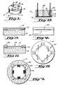
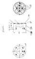
- FIGS. 19A and 19BOne approach for affixing pins or leads to a semiconductor substrate is to braze pins in place as illustrated in FIGS. 19A and 19B , respectively.
- FIG. 19Ais an example of a prior art brazing of a nail head pin to a substrate
- FIG. 19Bis an example of a prior art brazing of a headless pin to a substrate.
- FIG. 19Aillustrates a single crystal substrate 200 with a pin 210 that is brazed thereon.
- Pin 210includes a pin shaft 212 and a pin head 214 that provides a greater bonding surface area with substrate 200 .
- a braze 216is applied to the sides of pin head 214 . As illustrated via a stress fracture 218 , on a thin single crystal material stress fracture becomes a significant problem.
- substrate 200develops tensile stress as the melted braze hardens (or freezes) and contracts.
- the tensile stressconcentrates at the periphery of pin head 214 and promotes fracturing in the substrate.
- FIG. 19Banother approach to minimize stress in substrate 200 is to minimize the cross sectional area of the joint between substrate 200 and a headless pin 210 .
- the headless pinhelps to form a very small cross section joint with substrate 200 , however the newly formed joint is susceptible to high, localized stress from manipulation of the pin (back and forth—as shown by arrow 220 ) during subsequent manufacturing steps.
- a butt joint of this typeis considered an unreliable geometry because of the small attachment area and susceptibility to alignment problems.
- the inventionrelates generally to sensors and more particularly relates to a pressure and/or temperature sensor having exceptional stability up to 200° C. and effectively operable up to 700° C.
- the pressure sensor of the present inventionoperates without fluid fill and has no exterior exposed metallic components.
- the pressure sensorincludes a non-porous, impermeable surface that may be positioned in direct contact with fluids in an ultra-pure environment.
- the non-porous surfaceis comprised of a layer of single crystal sapphire that is impervious to chemical attack. In this manner, chemicals or contaminants cannot be extracted over time from the sensor into a process stream.
- the pressure sensor of the present inventionis suitable for use in chemically inert pressure transducer module or flow meter for sensing pressures in process fluids and may be molded directly into the high temperature plastic housing of the same.
- the present inventionprovides for a pressure sensor that includes a non-porous outer surface.
- the non-porous surfaceis characterized by a low diffusivity and low surface adsorption.
- the pressure sensorincludes a backing plate, a non-porous diaphragm, a sensing element adjacent an inner surface of the diaphragm, and a glass layer of a high strength material that is bonded by glassing to the backing plate and the non-porous diaphragm.
- the backing plateprovides rigidity to the structure. The rigidity of the backing plate resists stresses transmitted from the housing (not shown) to the sensing elements on the sensor diaphragm.
- the backing plateis not in direct contact with the process medium it is required to be mechanically stable and amenable to high temperature processes.
- the thermal expansion rate of the backing plateshould approximate closely that of the sensing diaphragm. While it is possible to compensate for thermal effects, a large mismatch will produce stresses during manufacture that may cause the bond between the two pieces to yield over time.
- the non-porous diaphragmmay include a Wheatstone bridge or a conductive layer formed thereon as part of a piezoresistive or capacitive type sensor respectively.
- a silicon layeris formed on an inner surface of the non-porous diaphragm, wherein a strain gage such as a Wheatstone bridge is formed thereon.
- the backing plateincludes apertures extending therethrough, the apertures being adapted for receiving electrical leads coupled to the sensing element.
- a change in pressure near the non-porous diaphragmis detectable by the sensing element.
- An increase and decrease of pressure against the diaphragmcauses deflection of the diaphragm, which in turn changes the resistances of the strain gage. The changes in resistance is correlated with the pressure adjacent the diaphragm.
- the non-porous diaphragmis preferably comprised of a chemically inert material such as sapphire.
- the glass layer between the sapphire and the backing plateis preferably made of high bond strength borosilicate glass or other glass of suitable known construction having a high bond strength and melt temperature above 700° C. and preferably above 1000° C.
- the amount that the diaphragm flexesis controlled by the thickness and diameter of the glass layer.
- the glass layermay have a thickness ranging between 0.002 and 0.030 inches with 0.010 inches being preferred and an outside diameter ranging from 0.100 to 2.0 inches with 0.700 inches being preferred.
- the active sensing area of the diaphragmmay range from 0.050 to 2.0 inches with 0.400 inches being preferred.
- the range of thickness and diameter of the diaphragmshould not be construed as limiting, but that the thickness and diameter in certain applications may be further reduced or increased as desired.
- the non-porous diaphragmengages an inner surface of the backing plate.
- the backing plate and non-porous diaphragmare constructed of materials having similar thermal expansion rates to avoid unnecessary stress through a wide range of temperatures.
- the pressure sensormay be constructed such that the sensing element may detect an absolute pressure or gage pressure.
- the pressure sensormay further include a silicon nitride layer and a metallization or conductive layer positioned between the silicon layer and the backing plate (see FIG. 11 ). In this manner the silicon nitride layer acts as an electrical insulator and the metallization layer blocks EMI/RFI from affecting the sensing element 20 .
- the pressure sensormay further include a coating, gasket or seal adjacent to at least a portion of an outer edge of the layers of the non-porous diaphragm, silicon nitride layer, metallization layer and the backing plate.
- acid resistant epoxy or corrosion resistant polymerssuch as PTFE (polytetrafluroethylene), PVDF (polyvinylidenefluoride), PEEK (polyetheretherketone), urethane, or Paralyne protection may be utilized, wherein an acid resistant epoxy is preferred.
- the pressure sensorincludes bond pads formed on the diaphragm between the glass layer and the non-porous diaphragm.
- the preferred embodiment of the bond padscomprise a titanium layer and a diffusion barrier.
- the doped silicon thin filminterconnects the bond pads in a known suitable manner to form the Wheatstone bridge.
- a windowis formed in the glass layer and backing plate, thereby providing access to bond pads.
- Electrical leadsextend through the windows formed in the glass layer and backing plate and the electrical leads are brazed to the bond pads. The electrical leads are brazed to the bond pads and the glass layer is glassed to the diaphragm and backing plate.
- the diaphragm and sensing elementis modified to create a capacitance rather than a piezoresistive sensor.
- the thin sensing diaphragmwhich flexes when pressure is applied, has a capacitive plate formed on the inner surface of the sensing diaphragm and another capacitive plate is formed on the inner surface of the backing plate.
- One electrical leadis connected to the capacitive plate formed on the inner surface of the sensing diaphragm and another lead is electrically coupled to the inner surface of the backing plate.
- the spacing between the diaphragm and the platevary with pressure the capacitance of the plate changes. This variation in capacitance is detected by an electrically connected sensing element of know suitable construction.
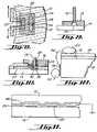
- FIG. 1is a perspective view of the pressure sensor of the present invention.
- FIG. 2is a partial sectional side elevational view of an embodiment of the pressure sensor of the present invention.
- FIG. 3is a partial sectional side elevational view of an embodiment of the pressure sensor of the present invention.
- FIG. 4is a partial sectional side elevational view of an embodiment of the pressure sensor of the present invention.
- FIG. 5is a partial sectional side elevational view of an embodiment of the pressure sensor of the present invention.
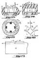
- FIG. 6is a top plan view of the diaphragm having a Wheatstone bridge formed thereon of the present invention.
- FIG. 7is a partial sectional top plan view of an embodiment of the diaphragm of the present invention.
- FIG. 8is a partial sectional top plan view of an embodiment of the bond pads of the present invention.
- FIG. 9is a partial sectional side elevational view of an embodiment of the bond pads of the present invention.
- FIG. 10is a partial sectional side clevational view of an embodiment of the bond pads of the present invention.
- FIG. 11is a partial sectional side elevational view of an embodiment of the pressure sensor of the present invention.
- FIG. 12is a partial sectional side elevational view of an embodiment of the pressure sensor of the present invention.
- FIG. 13is a partial sectional side elevational view of an embodiment of the pressure sensor of the present invention shown positioned in a pressure transducer housing.
- FIG. 14is a partial sectional side elevational view of an embodiment of the pressure sensor of the present invention shown molded into a pressure transducer housing.
- FIG. 15is a partial sectional top plan view of an embodiment of the diaphragm of the present invention.
- FIG. 16is an electrical schematic of an embodiment of the diaphragm of the present invention.
- FIG. 17is a partial sectional side elevational view of an embodiment of the pressure sensor of the present invention.
- FIG. 18is a partial sectional side elevational view of an embodiment of the pressure sensor of the present invention having a seal or gasket adjacent an edge of the sensor.
- FIG. 19Ais an example of a prior art brazing of a nail head pin to a substrate.
- FIG. 19Bis an example of a prior art brazing of a headless pin to a substrate.
- FIG. 20is a partial side view of a coil pin embodiment of the present invention that is brazed to a substrate according to the teachings of the present invention.
- FIG. 21is an exploded view of a sensor with coil spring leads that are brazed to the diaphragm according to the teachings of the present invention.
- FIG. 22is a side view of the assembled sensor of FIG. 21 .
- FIG. 23is an enlarged view of a coil spring lead of the present invention.
- the present inventionrepresents broadly applicable improvements to pressure sensors.
- the embodiments detailed hereinare intended to be taken as representative or exemplary of those in which the improvements of the invention may be incorporated and are not intended to be limiting.
- the pressure sensor of the present inventionmay be constructed as a piezoresistive or capacitive sensor having a sensing diaphragm.
- the sensing diaphragmis made of a piece of single crystal sapphire.
- the sensing diaphragmmay be constructed of a single crystal diamond.
- the sensor 10 of the present inventiongenerally comprises a backing plate 12 , sensing diaphragm 14 , silica glass bond 16 between the backing plate 12 and the diaphragm 14 , and electrical leads 18 (see FIGS. 1 and 2 ).
- a large wafer of the single crystal sapphireis used so that many sensors can be fabricated at the same time using the familiar planar processes of the semiconductor technology.
- sapphireis an electrical insulator.
- the silicon layercan, by diffusion, ion implantation, or other means be doped with atomic species such as boron or phosphorus to give the film semiconducting properties.
- atomic speciessuch as boron or phosphorus
- the area resistance value of the filmcan be adjusted.
- This filmin addition to having electrical resistance, will change its resistance in response to strain. This property is known as piezoresistance. As described earlier, deflection of the sensing diaphragm 14 will strain the film and produce a change in resistance. The pressure-sensing signal is derived from this change in resistance.
- the silicon patterns 20form a Wheatstone bridge 22 (see FIGS. 6 and 7 ). Those skilled in the art will appreciate that several different patterns can produce the Wheatstone bridge 22 .
- the silicon resistors 20may be patterned by standard photolithographic techniques. An insulating layer of silicon nitride 24 (see FIGS. 8 and 10 ) is applied to the entire surface of the sapphire wafer by chemical vapor deposition. Photolithographic resist is applied to the entire wafer. Windows are patterned in the resist and chemically removed.
- An acid itchantremoves the underlying nitride exposed by the window in the resist.
- a window 28is opened up above and adjacent to each of the connection points or bond pads 26 to the Wheatstone bridge (see FIG. 8 ).
- the silicon nitride layer 24is a tough insulating layer and further protects the delicate silicon layer.
- Metallic bond pads 26are needed to connect the electrical leads 18 to the Wheatstone bridge 22 .
- Metals commonly used as bond pads 26 in semiconductor devices such as gold and aluminumare unsuitable because they will alloy with the silicon at glassing temperatures.
- a two metal layer bond padis constructed (see FIG. 10 ).
- RFradio frequency
- Titaniumis a very active metal and has excellent bonding properties. Titanium, however, requires a diffusion barrier 32 between it and the braze material 34 .
- the braze alloy 34joins the bond pad 26 to pins 18 . Without a diffusion barrier 32 the braze 34 will alloy with both the titanium layer 30 and the thin silicon layer 20 .
- the diffusion barrier 32needs to be a refractory metal that will not form alloys at the brazing temperatures (approximately 1000° C.). Without limitation, niobium, tungsten, iridium, molybdenum, tantalum, platinum, and palladium are suitable for this purpose.
- the barrier material 32must be capable of being made into a film having a minimal amount of pinholes extending through the film. Any oxides must dissociate at brazing temperatures.
- Niobiumis found to work well as a diffusion barrier. The niobium is RF sputtered across the entire sapphire wafer 14 on the top of the titanium layer 30 . The niobium layer is then patterned using known lithographic techniques.
- the metal for the bond pads 26is deposited and patterned with methods know to those skilled in the art including, without limitation, evaporation and sputtering.
- the bond pad 26is patterned in such a way that the metal overlies (see FIG. 8 ) a portion of the silicon layer 20 but is primarily in direct contact with the sapphire diaphragm 14 .
- the reason for thisis that metallization layers may have small pinholes. It has been found that if the braze 34 is able to penetrate the diffusion barrier 32 it will alloy with the silicon with consequent failure of the film.
- the silica glass 16can serve to inhibit the flow of the braze 34 from the pin to the region where the bond pad 26 metal overlies the silicon pattern 20 .
- the braze 34must not overly the silicon pattern 20 .
- the sapphire waferis diced using known methods of dicing to separate the plurality of sapphire diaphragms from the sapphire wafer. Without limitation, several methods including scribe and fracture along crystal planes, ultrasonic machining, or laser cutting, may be utilized. The use of known methods allows for cutting round diaphragms 14 that are desirable for pressure sensor fabrication.
- the electrical leads 18are brazed to the bond pads 26 and the backing plate 12 is glassed to the diaphragm 14 .
- the thick backing plate 12 or waferis constructed of ceramic having holes or vias 36 (see FIG. 2 ).
- the vias 36are formed in the backing plate 12 to align with the bond pads 26 and provide passage of electrical leads 18 from the sensor diaphragm 14 to the electronics utilizing the pressure information.
- a vent hole 38is provided through the backing plate 12 when a gauge pressure sensing is desired.
- ceramicsconsist of metal oxide powders that are sintered together at high temperature typically using a small amount of glass to act as a binding agent.
- a common ceramicis alumina, which has many similar properties to single crystal sapphire. As long as the glass content of the alumina ceramic is kept below a few percent the thermal expansion properties of the two materials will be negligibly different.
- a glass 16 that will bind well to both sapphire and alumina ceramicneeds to have similar thermal expansion properties.
- Borosilicate glasseshave been found to be well suited for this purpose. These glasses have far higher melt temperatures than those glasses used for frit bonding materials together. It has been found that sensors fabricated from bulk silicon and exposed to temperatures above 600° C. experience excessive diffusion of dopant atoms into adjacent regions. Thus, these bulk silicon sensors are typically restricted to processing temperatures of no more than 450° C. and then for only brief excursions. As indicated by Ghiselin et al. in U.S. Pat. No. 4,774,843, reliable bonding of a sapphire diaphragm to a ceramic backing plate has been a significant problem.
- the proposed high bond strength borosilicate glasses used in glassingare distinct from lower temperature low strength solder glass or glass frit. The solder glass has a melt temperature around 450° C. and is of lower strength.
- a silica glass 16may be pre-formed or screened onto the surface of the backing plate 12 . In either case it is important that the silica glass does not flow far from where it starts. If the inner diameter of the glass pattern changes significantly the pressure characteristics of the sensor 10 can change drastically. Further, during the glassing process, if the glass 16 flows over the metallized bond pad 26 before the braze 34 on the bond pad 26 melts, the pins 18 will not braze to the bond pads 26 . The firing of the glass should be at constant temperatures to avoid leaving stresses in the glass bond that could result in instability or glass fracture. Further the silica glass 16 must have openings or windows for the electrical pins 18 .
- the sensing diaphragm 14will bottom out on the backing plate 12 during overpressure (see FIG. 4 ).
- this overpressure stopincreases the overpressure capacity of the sensor 10 by a factor of 100 or more.
- PN junctionsare used to form any diode or transistor and are used to isolate any features that are on a silicon wafer.
- To simply make a Wheatstone bridge on a silicon substraterequires a PN junction to isolate the bridge from the substrate semiconductor.
- PN junctionsare extremely useful they deteriorate quickly above 400° C. For most processes it is not possible to leave a device at 450° C. for more than 30 minutes otherwise it will be destroyed. It is also obviously not possible to have a process that may last 2–6 hours at temperatures as high as 900–1100° C. in order to make high stability bonds.
- the Wheatstone bridge of the present inventionis built directly on the sapphire diaphragm there is no PN junction therebetween that would cause a failure of the high melting temperature (above 400° C.).
- a PN junctionmay cause a breakdown of the glass bond of the diaphragm and back plate. Everywhere that a resistive surface is not needed the silicon is completely etched away.
- the braze alloy 34 used to bond the electrical lead 18 to the bond pad 26must melt at a temperature slightly below that of the silica glass 16 . Further, the braze 34 must be aggressive enough at its melt temperature to remove any oxides from the metal layers 26 . Without limitation, it has been found that several copper braze alloys of suitable known construction are capable of meeting these requirements. When the braze 34 melts before the glass 16 begins to flow, then if the silica glass 16 flows over the bond pad 26 it will flow over the braze 34 and bond pad 26 , thereby providing significant stress relief to the bond pad region. Without limitation, a braze alloy such as Pakusil-15 (comprised of palladium, copper, and silver) sold by Wesgo Metals, San Carlos, Calif., a Division of Morgan Advanced Ceramics Incorporated has been found to braze acceptably.
- Pakusil-15compact of palladium, copper, and silver
- the electrical lead or pin 18should be of a small cross section and preferably be made of a ductile metal. Such a pin 18 structures that confined by the geometry of the holes 36 in the ceramic backing plate 12 will have good strain relief properties and will not conduct stress from the pins 18 to the sensing elements. Pins 18 should be plated with a material with good braze and reasonable soldering capabilities such as nickel or gold.
- FIG. 20illustrates a partial side view of a coil pin embodiment of the present invention that is brazed to a silicon substrate according to the teachings of the present invention.
- Coil pin 250is brazed to substrate 251 at coil pin head 254 .
- at the foot of pin 250is a single circular coil 254 that is formed to function as the head of the pin.
- a springis formed at the end of the shaft with the spring portion being mounted on the substrate.
- a multi-coil springis used as the lead because of the case in fabrication and in maintaining 90 degrees alignment with the substrate.
- coil pin 259is more flexible than a solid head pin illustrated in FIG. 19A .
- a materialsuch as Kovar or Invar it is possible to reduce the stresses by a factor of 10 or more.
- the pinhas a length of about 0.320 inches, an outside diameter of coil 0.040 inches, and a wire diameter of about 0.008 inches.
- wire diameterOne important consideration in connection with the structure of the pin is the wire diameter. A preferred range of wire diameter dimensions is about 0.001 inches to about 0.020 inches.
- Another important design consideration to the structure of the wireis that the stiffness of wire increases with the 4 th power of the diameter. Nickel is preferred material for the lead, but Kovar works as well.
- a preferred braze compositionis comprised of 65% silver, 20% copper, and 15% palladium.
- Various copper-silver combinationsare used to obtain melt temperatures near those of borosilicate glasses ( ⁇ 900° C.), however the amount of palladium used does affect the melt temperature of the braze.
- the more palladium is used in the compositionthe higher the melt temperature for the braze material.
- Palladiumalso plays an important role in the braze composition in controlling the viscosity of the braze melt puddle. The viscosity of both silver and copper at melt temperature is known to be very low. Both these materials will readily migrate to adjacent regions both horizontally and vertically through thin film dielectrics.
- the braze materialhas a thickness of about 0.0001 to about 0.0002 inches.
- braze processesthere are a number of braze processes that would be utilized in connection with the present invention. It is preferable to use a belt furnace process that allows the glass and brazing to take place in a single process. This approach is a cost savings but is not essential to the function of the braze joint.
- nickelis used as the pin or lead material such that nickel does not closely match the expansion coefficient but has very low yield strength. While the expansion rate may be high the strength of the substrate crystalline structure and the braze material can overwhelm the strength of a small cross-section coil of wire. To compensate the coil portion is joined not only at the braze end but also at the other end where it is attached to the circuit board, wire or flex circuit. For this reason a material that solders easily is desirable. Gold, platinum, and nickel all meet this requirement with nickel having the lowest cost.
- the high temperature capabilities of all of the materials of construction of the sensor 10allows use of such sensor 10 at very high temperatures (above 400° C.) over extended periods of time and/or such sensor 10 may be molded directly into high performance plastic housings such as PFA (generic name) TEFLON® (“Teflon” is a registered trademark of E. I. DuPont DeNemours and Company) (see FIG. 14 ).
- PFAgenerator name
- TEFLON®is a registered trademark of E. I. DuPont DeNemours and Company
- First dotted line identified by 40represents a greatly exaggerated flexure of the diaphragm 14 .
- Second dotted line identified by 42represents a flexure of the diaphragm due to overpressure (disregarding the stopping affect the backing plate 12 has on flexure of the diaphragm during overpressure). Such drastic flexure would likely fracture or break the diaphragm 14 .
- FIG. 5shows a modified diaphragm 14 , having thinner central portions of the diaphragm than the outer portion of the diaphragm.
- the thickness of the diaphragmshould decrease for maximum sensitivity.
- the gap between the diaphragm 14 and backing plate 12may be controlled by the thickness of the glass bond 16 .
- the glass thicknessis minimized to improve the stiffness of the structure.
- a shallow depression (2 to 5 mils)is created in ceramic 12 at the time of molding. Under overpressure conditions the sapphire bottoms out on the interior surface of ceramic 12 and the flexural stress on sapphire diaphragm 14 is thereby limited.
- a typical flexure of the diaphragmis between 0.01 to 0.0001 inches and the spacing may be between 0.02 to 0.0002 inches depending upon the thickness and diameter of the diaphragm 14 .
- the order of magnitude of the gapis preferably twice the thickness of the diaphragm 14 .
- the active sensing region of the diaphragmmay range between 0.075 to 2 inches for a diaphragm having a thickness ranging from 0.002 to 0.050 inches.
- Practical constraintslimit the thickness of a single crystal sapphire wafer during wafer fabrication. Unlike single crystal silicon, however, there is no easy method of forming thin sapphire diaphragms by chemical processes.
- the modified diaphragm 14 shown in FIG. 5reduces the thickness of the diaphragm proximate the sensing area while being manufactured from a thicker sapphire wafer. Thinning the diaphragm after thin film processing has been completed allows for more compliant pressure sensing diaphragms. A rim of material left around each device provides strength required, for example, when the sensing diaphragm is in direct contact with a pressure sensor housing. The thin central area 46 provides the sensitivity required.
- the sapphire diaphragm 14can be thinned by conventional mechanical means such as abrasive machining or ultrasonic machining known to those skilled in the art.
- annular groove 80may be formed on the outer sensing surface of the diaphragm 14 (see FIG. 17 ).
- shape of the grooveis not critical, rounded edges and groove is preferred.
- the grooveis annular, other geometric shapes may be adequate to relieve flexure stress in the region adjacent the glass bond 16 .
- FIG. 11an alternate embodiment of the pressure sensor of the present invention is shown having a conductive layer sandwiched between the backing plate 12 and the silicon nitride layer 24 .
- the conductive layer 48is shown electrically grounded. In this manner electromagnetic and radio frequency interference (EMI and RFI) are blocked. EMI and RFI are known to degrade the performance of piezoresistive sensors. Because of the epitaxial construction of silicon on sapphire and the desire to bond the silicon directly to the sapphire, it is not possible to put a conductive layer between the silicon and the sapphire. Further, putting a conductive layer on the outside of the sapphire diaphragm would defeat the non-porous, chemically inert attributes of the sapphire diaphragm.
- the conductive or metallization layer 48may comprise a layer of niobium, tungsten, iridium, molybdenum, tantalum, platinum, and palladium, or other material known to shield EMI and RFI.
- the metal layer 48shields the sensing element from EMI and RFI originating from above the conductive layer.
- the EMI and RFIwill set up standing waves with zero potential at the conductive layer 48 . It is known that if the radiation of the standing waves has frequency components whose wavelength is on the order of the distance between the ground plane and the resistive components, significant interference will result. If, on the other hand, the distance from the ground plane to the resistive component is small, then the standing waves will have negligible amplitude at the location of the piezoresistive element and no interference will occur. Since EMI and RFI interference occurs in the range of 1 MHz to 1,000 MHz, the minimum wavelength for this frequency range is 0.3 meters.
- the distance between the ground plane and the piezoresistive elements or the silicon pattern 20is equivalent to the thickness of the silicon nitride layer, which is one the order of 500 Angstrrom's or 0.00000005 meters.
- the expected effectiveness of EMI and RFI shieldingis approximately 6,000,000:1.
- a non-porous chemically inert pressure sensormay be used advantageously to detect pressures in a highly caustic environment. Sensors having a sensing diaphragm constructed with single crystal sapphire provide excellent protection against chemical attack.
- the sensor 10may be positioned within a pressure transducer housing 50 (see FIG. 13 ) having primary and secondary seals 52 and 54 . If the primary seal engages the outer surface of the sapphire diaphragm, the process fluid wets only the seal and the sapphire. Since seals of known suitable construction are permeable to process fluids, some process fluid will get beyond the primary seal.
- Very aggressive process fluids such as hydrofluoric acid permeate past the first primary sealmay attack the joint between the sapphire diaphragm 14 and the ceramic backing plate 12 .
- the contaminants from the corrosion of the jointmay then permeate back into the process fluids.
- the present inventionmay include a chemically resistant polymer such a an acid resistant epoxy, for example without limitation, acid resistant epoxy EP21AR available from Master Bond, Inc. of Hackensack, N.J. applied to the edge of the sensor 10 surrounding the joint.
- a gasket type sealmade of, for example without limitation, TEFLON, or an elastomeric type seal 84 made of, for example without limitation, KALREZ, may be compressed against the joint of the sensor as shown in FIG. 18 .
- the seal 84has an L-shaped cross-section and may wrap around the side of the sensor 10 and onto the diaphragm 14 sensing outer surface.
- the gasket seal 84may be formed as part of the housing 50 .
- the materialcould be made electrically conductive by blending in carbon powder.
- the conductive epoxycould be connected to an electrical ground by means of conductive ink 58 which is coupled to the ground.
- the senoris coated (including the sapphire surface) with Paralyne so as to limit chemical extraction from the sapphire and into the process fluids when the sensor is in use.
- the sensorcan also be coated with PFA to also limit chemical extraction from the sapphire diaphragm.
- the sensor 10is shown positioned within a pressure transducer housing 50 having fluid port 60 .
- the sapphire diaphragmseals against the primary and secondary seals 52 and 54 .
- a vent or drain 62may extend from the outside of the pressure transducer housing into the housing between the primary and secondary seal. The vent 62 may relieve pressure between the seals and/or provide a passage for fluids permeating through the primary seal to exit out the pressure transducer housing 50 .
- the sensor 10 of the present invention having a sapphire diaphragm 14provides a pressure sensor that is corrosion and solvent resistant, has desired flexure with no measurable temperature or pressure hysteresis, and can tolerate process fluid temperatures exceeding 400° C. Referring to FIG.
- the pressure sensorsince the pressure sensor is able to withstand high temperatures, the pressure sensor may alternatively be molded into the plastic housing 50 of the pressure transducer as an insert during the plastic injection molding process, thereby eliminating the need for a primary or secondary seal.
- the housingitself acts as a seal to the sensor 10 .
- Such mold in place pressure sensor and moduleis expected to reduce production costs, simplify construction and decrease the overall size of the pressure transducer module.
- the sensor 10is capable of detecting both the pressure and temperature of the fluid adjacent the diaphragm 14 .
- Bond pads 72are formed on the sensor in a similar manner and at the same time as bond pads 26 .
- the resistor 70is formed between the glass bond 16 and the diaphragm 14 . By positioning the resistor outside the pressure stress zone, pressure induced stresses that may affect the resistance of resistor 70 are thereby avoided.
- the resistance of the single crystal silicon resistor 70has well-defined temperature dependence. It has been found that for high doping concentrations (p doping above 10 19 atoms/cc) the function between temperature and resistance closely approximates a linear function. Thus, as resistance changes the temperature change is readily determinable.
- FIG. 16shows another embodiment of the sensor 10 , wherein the resistors of the Wheatstone bridge 22 are utilized to both determine pressure and temperature.
- the outer periphery of sensor 10is represented by a dotted line.
- the resistance of the single crystal silicon resistors that comprise the Wheatstone bridgehave well-defined temperature dependence.
- a resistor 76 designated as “Rt” in FIG. 16is electrically coupled to the Wheatstone bridge 22 but is of zero temperature coefficient construction.
- a metal film resistormeets this requirement.
- the resistor 76may be located with the sensing electronics of a pressure transducer and remote from the diaphragm 14 .
- the value of the resistor 76is preferably approximately half of the value of the Wheatstone bridge 22 resistance.
- the voltage Vtwill depend almost entirely upon the temperature of the Wheatstone bridge 22 , especially if the silicon resistors are heavily doped. If the silicon resistors are lightly doped or if the user desires to reduce the uncertainty in the measurement of temperature, the temperature can be derived by a matrix characterization.
- coefficients a xxare obtained by a least squares fitting procedure known to those skilled in the art. Utilization of the above characterization along with the data fitting procedure will provide a sensor with a calibrated temperature output that is calibrated for strain effects. Thus, the simultaneous measurement of pressure and temperature from a single sensor is achieved with quick response times. Alternatively, if only temperature output is desired, pressure characterization can be avoided by orienting the legs of the resistor in the axis that is not strain sensitive. For example, maximum strain sensitivity of R-plane silicon on sapphire is attained by orienting the resistor elements 45 degrees to the projected C-axis, where the R-plane and C-axis are defined by Miller indices of crystal geometry.
- Piezoresistanceis zero for resistor elements aligned parallel or perpendicular to the projected C-axis.
- the axis of the resistorscan be rotated to eliminate pressure sensitivity. In this manner, sensor 10 could be made to eliminate pressure sensitivity and to, thus, only determine temperature proximate the sensor 10 .
- High temperature glass seals(above 700° C.) are much stiffer and have less hysteresis than low temperature bonding methods (typical 450° C. glass). The high temperature sealing process, however, will destroy any structure (bond pad) needed for traditional wire bonding.
- the conventional alternative to wire bondingis conductive epoxy, however conductive epoxy has a tendency to oxidize and increase in resistance over time. This increase in resistance results in an output shift of the sensor.
- the brazing process and the electrical lead configuration of the present inventionprovides an effective solution to this problem.
- Silver and copperare ineffective when used as brazing materials because they tend to diffuse quickly into the silicon or silicon substrate and damage electrical/electronic structures that are displaced far away from the location that they were melted.
- palladiumis used to increase the viscosity of the fluid braze puddle during heating and acts to control the migration of silver and copper.
- FIGS. 21 and 22illustrate a related sensor embodiment, sensor 10 A (either pressure, temperature or both) of the present invention that is configurable as a piezoresistive or capacitive sensor having a sensing diaphragm 14 A.
- Sensing diaphragm 14is made of a piece of single crystal sapphire. Alternatively, the sensing diaphragm may be constructed of a single crystal diamond.
- Sensor 10 A of the present inventiongenerally comprises a backing plate 12 A, sensing diaphragm 14 A, a silica glass perform plate 16 A (preferably borosilicate glass—of high temperature (over 700° C. and having high strength) used to form the glass bond between the backing plate 12 and the diaphragm 14 , and coil spring electrical leads 18 A.
- backing platehas apertures 36 A that extend therethrough, and accommodate the leads, and includes at least one offset vent hole 38 A.
- the sapphire diaphragmhas a diameter of about 0.695 inches and is preferably slightly smaller in diameter than silica plate 16 .
- Preformed silica plate 16has an outside diameter of about 0.710 inches, an inside diameter of about 0.380 inches and is about 0.010 inches in thickness.
- Apertures 17 A, which accommodate the leads,have a diameter of about 0.050 inches and are disposed on an imaginary inner ring having a diameter of about 0.545 (see FIG. 22 ).
- Preformed braze alloy 34 Ais preferably a composite material made of palladium, copper and silver (65% Ag., 20% Cu.; and 15% Pd.) and has a diameter of about 0.047+/ ⁇ 0.002 inches and a thickness of about 0.002+/ ⁇ 0.001 inches. Once the braze material has melted onto the lead, the pull strength should be a minimum of 2 pounds.
- Backing plate 14 Ais 96% alumina and has a diameter of about 0.710+/ ⁇ 0.005 inches and has a thickness of about 0.240+/ ⁇ 0.005 inches.
- Apertures 36 Ahave a diameter of about 0.050 inches while vent hole 38 A has a diameter that tapers (in this embodiment) from a diameter of 0.050 to 0.032 inches. The tapered end is disposed adjacent the diaphragm.
- FIG. 22A side view of sensor 10 A, shown in FIG. 22 , illustrates that about 20% of leads 18 A protrude above backing plate 12 A.
- the coil spring lead 18 Ahas a length preferably of 0.32 inches and is preferably comprised of, but is not necessarily limited to, two dead coil portions 19 A and an expanded middle coil portion 19 B.
- a dead coil portion 19 Aprotrudes about 20% of its length from backing plate 12 A.
- the coilspreferably have a diameter of about 0.036 inches to about 0.042 inches.
- Nickelis preferably used to form the coil spring leads because of its pliability.
- Kovarcan also be used to form the coil spring leads, but it is a more difficult material to work with because of its stiffness.
- the coil spring lead configuration described above and illustrated in FIG. 23can also be used in other electronic applications where flexibility in the lead is preferred and there is a concern for fracturing the underlying substrate.
- the weight usedis made of stainless steel and weighs about 100 grams per square inch of sealing surface.
- the stainless steelis preferred because it does not react to the other materials in the process but the weight can be made of other non-reacting materials.
- the weightis preferably placed on the side of the backing plate that has leads 18 A protruding therefrom.
- the glass bondis formed and the leads are brazed in a single heating/melting operation, such as subjecting the entire assembly to a belt furnace.
- the backing plate and diaphragmare glass-bonded together first.
- the braze materialis then placed into the apertures along with the leads and the assembly is subjected to a brazing temperature of about 925° C. and then slowly cooled (about 7–10° C. per minute) to avoid substrate fracturing, the entire operation lasting about 2 hours.
- the processing timewill vary depending on the thermal mass of the sensor being manufactured (e.g., the bigger the sensor the longer the cooling time).
- Another step in the processing of the sensoris to preferably form the glass bond and the brazing in a non-oxidizing environment. Oxygen that is present during the brazing process will cause oxidation of the semiconductor surfaces thereby interfering with the mechanical and conductive joints to be formed between the brazed lead and the sensing element on the diaphragm.
- Oxygen that is present during the brazing processwill cause oxidation of the semiconductor surfaces thereby interfering with the mechanical and conductive joints to be formed between the brazed lead and the sensing element on the diaphragm.
- One approachis to use argon or nitrogen gas to substitute for oxygen in the chamber where the sensor is formed.
- Another approachis to use vacuum brazing at a high temperature (above 1050° C.) to avoid oxidation of the device surfaces.
Landscapes
- Physics & Mathematics (AREA)
- General Physics & Mathematics (AREA)
- Electromagnetism (AREA)
- Chemical & Material Sciences (AREA)
- Analytical Chemistry (AREA)
- Measuring Fluid Pressure (AREA)
- Ceramic Products (AREA)
Abstract
Description
T=a00+a01VT+a02VT2+ . . . +a10VP+a11VPVT+a12VPVT2+ . . . +a20VP2+ . . .
Claims (18)
Priority Applications (6)
| Application Number | Priority Date | Filing Date | Title |
|---|---|---|---|
| US10/440,433US7152478B2 (en) | 2000-07-20 | 2003-05-16 | Sensor usable in ultra pure and highly corrosive environments |
| CN200480016930ACN100587435C (en) | 2003-05-16 | 2004-05-14 | Sensors available in ultra-high purity and highly corrosive environments |
| JP2006533058AJP5033421B2 (en) | 2003-05-16 | 2004-05-14 | Sensor usable in ultrapure environment and highly corrosive environment, and its manufacturing method |
| KR1020057021825AKR101107464B1 (en) | 2003-05-16 | 2004-05-14 | Sensor having a non-porous outer surface and method of bonding an electrical lead to a semiconductor device |
| PCT/US2004/015098WO2004105091A2 (en) | 2003-05-16 | 2004-05-14 | Sensor usable in ultra pure and highly corrosive environments |
| TW093113740ATWI341920B (en) | 2003-05-16 | 2004-05-14 | A sensor having non-porous outer surface ,an electrical lead member,and a method of bonding an electrical lead to a semiconductor device |
Applications Claiming Priority (2)
| Application Number | Priority Date | Filing Date | Title |
|---|---|---|---|
| US09/620,007US6612175B1 (en) | 2000-07-20 | 2000-07-20 | Sensor usable in ultra pure and highly corrosive environments |
| US10/440,433US7152478B2 (en) | 2000-07-20 | 2003-05-16 | Sensor usable in ultra pure and highly corrosive environments |
Related Parent Applications (1)
| Application Number | Title | Priority Date | Filing Date |
|---|---|---|---|
| US09/620,007Continuation-In-PartUS6612175B1 (en) | 2000-07-20 | 2000-07-20 | Sensor usable in ultra pure and highly corrosive environments |
Publications (2)
| Publication Number | Publication Date |
|---|---|
| US20040040382A1 US20040040382A1 (en) | 2004-03-04 |
| US7152478B2true US7152478B2 (en) | 2006-12-26 |
Family
ID=33476595
Family Applications (1)
| Application Number | Title | Priority Date | Filing Date |
|---|---|---|---|
| US10/440,433Expired - LifetimeUS7152478B2 (en) | 2000-07-20 | 2003-05-16 | Sensor usable in ultra pure and highly corrosive environments |
Country Status (6)
| Country | Link |
|---|---|
| US (1) | US7152478B2 (en) |
| JP (1) | JP5033421B2 (en) |
| KR (1) | KR101107464B1 (en) |
| CN (1) | CN100587435C (en) |
| TW (1) | TWI341920B (en) |
| WO (1) | WO2004105091A2 (en) |
Cited By (15)
| Publication number | Priority date | Publication date | Assignee | Title |
|---|---|---|---|---|
| US20090000372A1 (en)* | 2005-03-18 | 2009-01-01 | Masahiro Matsumoto | Thermal Flow Measurement Device |
| US20090071259A1 (en)* | 2007-02-16 | 2009-03-19 | Hiroaki Tanaka | Pressure Sensor and Manufacturing Method Thereof |
| US20090078041A1 (en)* | 2007-09-20 | 2009-03-26 | Yamatake Corporation | Flow sensor unit |
| US20090139338A1 (en)* | 2007-09-28 | 2009-06-04 | James Tjan-Meng Suminto | Silicon sensing structure to detect through-plane motion in a plane of material with thermal expansion substantially different from that of silicon |
| US20090158853A1 (en)* | 2007-12-20 | 2009-06-25 | Walter Christian Berner | Diaphragm pressure measuring cell arrangement |
| US20110083513A1 (en)* | 2008-04-28 | 2011-04-14 | Christian Wohlgemuth | Pressure Sensor |
| US20110203381A1 (en)* | 2006-06-15 | 2011-08-25 | Kulite Semiconductor Products, Inc. | Corrosion-resistant high temperature pressure transducer employing a metal diaphragm |
| US20110221456A1 (en)* | 2010-03-11 | 2011-09-15 | General Electric Company | Sensor system and methods for environmental sensing |
| US8141429B2 (en)* | 2010-07-30 | 2012-03-27 | Rosemount Aerospace Inc. | High temperature capacitive static/dynamic pressure sensors and methods of making the same |
| US20150033878A1 (en)* | 2012-03-06 | 2015-02-05 | Centre National De La Recherche Scientifique Laboratoire D'analyse Et D'archit | Method for producing a pressure sensor and corresponding sensor |
| US20150219514A1 (en)* | 2014-02-05 | 2015-08-06 | Mgi Coutier | Pressure and temperature determining device, pressure and temperature sensor comprising such a device and method for manufacturing such a device |
| US20160223378A1 (en)* | 2015-02-02 | 2016-08-04 | Mgi Coutier | Pressure and temperature determining device, a pressure and temperature sensor comprising such a device and a method for manufacturing such a device |
| US9890033B2 (en) | 2015-04-06 | 2018-02-13 | Honeywell International Inc. | Silicon-on-sapphire device with minimal thermal strain preload and enhanced stability at high temperature |
| US9975765B1 (en) | 2015-12-18 | 2018-05-22 | The United States Of America As Represented By The Administrator Of National Aeronautics And Space Administration | Fabricating ultra-thin silicon carbide diaphragms |
| US10330549B2 (en) | 2013-05-17 | 2019-06-25 | Endress+Hauser Se+Co.Kg | Ceramic pressure measurement cell and method for production thereof |
Families Citing this family (29)
| Publication number | Priority date | Publication date | Assignee | Title |
|---|---|---|---|---|
| AT410498B (en)* | 2001-02-20 | 2003-05-26 | Akg Acoustics Gmbh | ELECTROACOUSTIC CAPSULE |
| JP2003315193A (en)* | 2002-04-24 | 2003-11-06 | Denso Corp | Pressure sensor |
| JP5558667B2 (en)* | 2004-09-29 | 2014-07-23 | ローズマウント インコーポレイテッド | Pressure transducer with improved process adapter |
| US7713771B2 (en)* | 2006-09-01 | 2010-05-11 | Grundfos A/S | Pressure sensor |
| US7845546B2 (en)* | 2007-04-07 | 2010-12-07 | Inficon Gmbh | Method for producing a vacuum measuring cell of the membrane type |
| AT505077B1 (en)* | 2008-06-06 | 2010-01-15 | Avl List Gmbh | MEASURING DEVICE |
| US7992441B2 (en)* | 2008-07-31 | 2011-08-09 | Sensata Technologies, Inc. | Pressure sensor for measuring pressure in a medium |
| US9126271B2 (en)* | 2008-10-07 | 2015-09-08 | Wisconsin Alumni Research Foundation | Method for embedding thin film sensor in a material |
| FI125815B (en) | 2010-10-14 | 2016-02-29 | Janesko Oy | Measuring sensor to measure temperature |
| WO2012131788A1 (en)* | 2011-03-31 | 2012-10-04 | シチズンファインテックミヨタ株式会社 | Cylinder internal-pressure sensor for engine |
| ITMI20120456A1 (en)* | 2012-03-23 | 2013-09-24 | Microtel Tecnologie Elettroniche S P A | CERAMIC PRESSURE SENSOR AND RELATIVE PRODUCTION METHOD, AND TRANSDUCER THAT INCORPORATES A CERAMIC PRESSURE SENSOR |
| EP2720019A1 (en)* | 2012-10-10 | 2014-04-16 | Auto Industrial Co., Ltd. | Pressure transducer using ceramic diaphragm |
| US8943896B2 (en) | 2012-10-10 | 2015-02-03 | Auto Industrial Co., Ltd. | Pressure transducer using ceramic diaphragm |
| US9391002B2 (en) | 2013-11-21 | 2016-07-12 | Amphenol Thermometrics, Inc. | Semiconductor sensor chips |
| US20150137277A1 (en)* | 2013-11-21 | 2015-05-21 | General Electric Company | Semiconductor sensor chips |
| JP6243762B2 (en)* | 2014-03-14 | 2017-12-06 | サーパス工業株式会社 | Pressure sensor |
| DE102015105057A1 (en)* | 2015-04-01 | 2016-10-06 | Endress + Hauser Gmbh + Co. Kg | Capacitive pressure sensor |
| KR101661443B1 (en) | 2016-06-02 | 2016-09-29 | 강성중 | Flexible lead manufacturing methods |
| CN110573286A (en)* | 2016-09-22 | 2019-12-13 | 鲁科斯-钎焊材料有限公司 | Solder Nail Head Leads |
| JP6751648B2 (en)* | 2016-10-27 | 2020-09-09 | サーパス工業株式会社 | Pressure detector |
| US10823630B1 (en) | 2016-11-11 | 2020-11-03 | Iowa State University Research Foundation, Inc. | High sensitivity MEMS pressure sensor |
| DE102017109226A1 (en)* | 2017-04-28 | 2018-10-31 | Testo SE & Co. KGaA | Deep-frying oil and / or frying fat sensor for determining a frying oil and / or frying fat quality |
| DE102017213527A1 (en)* | 2017-08-03 | 2019-02-07 | Robert Bosch Gmbh | A method of manufacturing a pressure sensor means for measuring a pressure of a fluid and pressure sensor means for measuring a pressure of a fluid |
| JP6922788B2 (en)* | 2018-03-05 | 2021-08-18 | 三菱電機株式会社 | Semiconductor pressure sensor |
| JP7372062B2 (en)* | 2019-07-02 | 2023-10-31 | アズビル株式会社 | pressure sensor |
| US11378480B2 (en)* | 2020-09-21 | 2022-07-05 | Rosemount Inc. | Polysilicon on sapphire oil-less pressure sensor |
| CN116235022A (en)* | 2020-09-29 | 2023-06-06 | 森萨塔科技公司 | Junction isolation semiconductor strain gauge |
| US12422307B2 (en)* | 2021-10-22 | 2025-09-23 | Matthew A. Hertel | MEMS thermal sensor array |
| DE102023127186A1 (en)* | 2023-10-05 | 2025-04-10 | Endress+Hauser SE+Co. KG | Pressure sensor for determining a first pressure of a medium |
Citations (71)
| Publication number | Priority date | Publication date | Assignee | Title |
|---|---|---|---|---|
| US3916365A (en) | 1972-01-31 | 1975-10-28 | Bailey Motor Company | Integrated single crystal pressure transducer |
| US3930823A (en) | 1972-03-14 | 1976-01-06 | Kulite Semiconductor Products, Inc. | High temperature transducers and housing including fabrication methods |
| US3946615A (en) | 1975-06-09 | 1976-03-30 | Bourns, Inc. | Pressure transducer |
| US4016644A (en) | 1974-03-18 | 1977-04-12 | Kulite Semiconductor Products, Inc. | Methods of fabricating low pressure silicon transducers |
| US4065970A (en) | 1976-05-17 | 1978-01-03 | Becton, Dickinson Electronics Company | Diffused semiconductor pressure gauge |
| US4127840A (en) | 1977-02-22 | 1978-11-28 | Conrac Corporation | Solid state force transducer |
| US4151578A (en) | 1977-08-01 | 1979-04-24 | Kavlico Corporation | Capacitive pressure transducer |
| US4161887A (en) | 1977-09-02 | 1979-07-24 | Bourns, Inc. | Media independent differential pressure transducer |
| US4177496A (en) | 1976-03-12 | 1979-12-04 | Kavlico Corporation | Capacitive pressure transducer |
| US4202217A (en) | 1977-12-12 | 1980-05-13 | Kulite Semiconductor Products, Inc. | Semiconductor transducers employing flat bondable surfaces with buried contact areas |
| US4203327A (en) | 1978-06-29 | 1980-05-20 | Honeywell Inc. | Piezoresistive silicon strain sensors and pressure transducers incorporating them |
| US4207604A (en) | 1976-12-02 | 1980-06-10 | Kavlico Corporation | Capacitive pressure transducer with cut out conductive plate |
| US4227419A (en) | 1979-09-04 | 1980-10-14 | Kavlico Corporation | Capacitive pressure transducer |
| US4236137A (en) | 1979-03-19 | 1980-11-25 | Kulite Semiconductor Products, Inc. | Semiconductor transducers employing flexure frames |
| US4291293A (en) | 1978-09-27 | 1981-09-22 | Hitachi, Ltd. | Semiconductor absolute pressure transducer assembly and method |
| US4329732A (en) | 1980-03-17 | 1982-05-11 | Kavlico Corporation | Precision capacitance transducer |
| US4345476A (en) | 1980-07-25 | 1982-08-24 | Bourns Instruments, Inc. | Differential pressure transducer with high compliance, constant stress cantilever beam |
| US4347745A (en) | 1980-12-22 | 1982-09-07 | Bourns Instruments, Inc. | Pressure measuring apparatus |
| US4373399A (en) | 1981-02-05 | 1983-02-15 | Beloglazov Alexei V | Semiconductor strain gauge transducer |
| US4395915A (en) | 1981-10-06 | 1983-08-02 | Bourns Instruments, Inc. | Pressure measuring apparatus |
| US4398426A (en) | 1981-07-02 | 1983-08-16 | Kavlico Corporation | Linear capacitive pressure transducer system |
| US4425799A (en) | 1982-06-03 | 1984-01-17 | Kavlico Corporation | Liquid capacitance pressure transducer technique |
| US4426673A (en) | 1976-03-12 | 1984-01-17 | Kavlico Corporation | Capacitive pressure transducer and method of making same |
| US4439752A (en) | 1981-10-26 | 1984-03-27 | Honeywell Inc. | Semiconductor pressure transducer |
| US4501051A (en) | 1981-05-11 | 1985-02-26 | Combustion Engineering, Inc. | High accuracy differential pressure capacitive transducer and methods for making same |
| US4535283A (en) | 1983-04-18 | 1985-08-13 | Gosudarstvenny Nauchno-Issledovatelsky Institut Teploenergeticheskogo Priborostroenia | Device for conversion of non-electrical quantity into electrical signal |
| US4574640A (en) | 1984-11-29 | 1986-03-11 | Bourns Instruments, Inc. | Integrated dual-range pressure transducer |
| US4586109A (en) | 1985-04-01 | 1986-04-29 | Bourns Instruments, Inc. | Batch-process silicon capacitive pressure sensor |
| US4600912A (en) | 1985-01-25 | 1986-07-15 | Bourns Instruments, Inc. | Diaphragm pressure sensor with improved tensile loading characteristics |
| US4656454A (en) | 1985-04-24 | 1987-04-07 | Honeywell Inc. | Piezoresistive pressure transducer with elastomeric seals |
| US4665754A (en) | 1985-04-08 | 1987-05-19 | Honeywell Inc. | Pressure transducer |
| US4725406A (en) | 1985-10-21 | 1988-02-16 | American Bionetics, Inc. | Apparatus and method for diagnostic analysis of biological fluids |
| US4735917A (en) | 1986-04-28 | 1988-04-05 | General Electric Company | Silicon-on-sapphire integrated circuits |
| US4751554A (en) | 1985-09-27 | 1988-06-14 | Rca Corporation | Silicon-on-sapphire integrated circuit and method of making the same |
| US4765188A (en) | 1986-11-24 | 1988-08-23 | Bourns Instruments, Inc. | Pressure transducer with integral digital temperature compensation |
| US4773269A (en) | 1986-07-28 | 1988-09-27 | Rosemount Inc. | Media isolated differential pressure sensors |
| US4774843A (en) | 1987-08-14 | 1988-10-04 | Gulton Industries, Inc. | Strain gage |
| US4864463A (en) | 1988-04-19 | 1989-09-05 | Allied-Signal Inc. | Capacitive pressure sensor |
| US4876892A (en) | 1988-04-19 | 1989-10-31 | Allied-Signal Inc. | Pressure sensor |
| US4903000A (en) | 1987-12-03 | 1990-02-20 | Ngk Insulators, Ltd. | Pressure sensor having means for electromagnetically shielding resistors |
| US4987782A (en) | 1989-10-03 | 1991-01-29 | Allied-Signal Inc. | Capacitive pressure transducer system |
| US4994781A (en) | 1988-04-07 | 1991-02-19 | Sahagen Armen N | Pressure sensing transducer employing piezoresistive elements on sapphire |
| US4999735A (en) | 1990-03-08 | 1991-03-12 | Allied-Signal Inc. | Differential capacitive transducer and method of making |
| US5005421A (en) | 1988-07-22 | 1991-04-09 | Endress U. Hauser Gmbh U. Co. | Pressure sensor and method for the manufacture thereof |
| US5024097A (en) | 1987-01-28 | 1991-06-18 | U.S. Philips Corporation | Pressure sensor comprising a silicon body |
| US5050035A (en) | 1989-03-21 | 1991-09-17 | Endress U. Hauser Gmbh U. Co. | Capacitive pressure sensor and method of manufacturing same |
| US5050034A (en) | 1990-01-22 | 1991-09-17 | Endress U. Hauser Gmbh U. Co. | Pressure sensor and method of manufacturing same |
| US5076147A (en) | 1989-04-13 | 1991-12-31 | Endress U. Hauser Gmbh U. Co. | Pressure sensor including a diaphragm having a protective layer thereon |
| US5079953A (en) | 1989-08-04 | 1992-01-14 | Endress U. Hauser Gmbh U. Co. | Pressure gage |
| US5088329A (en) | 1990-05-07 | 1992-02-18 | Sahagen Armen N | Piezoresistive pressure transducer |
| US5097712A (en) | 1989-09-28 | 1992-03-24 | Endress U. Hauser Gmbh U. Co. | Differential pressure measuring apparatus |
| US5111698A (en) | 1989-10-06 | 1992-05-12 | Endress U. Hauser Gmbh U. Co. | Differential pressure measuring apparatus |
| US5155061A (en) | 1991-06-03 | 1992-10-13 | Allied-Signal Inc. | Method for fabricating a silicon pressure sensor incorporating silicon-on-insulator structures |
| US5174926A (en) | 1988-04-07 | 1992-12-29 | Sahagen Armen N | Compositions for piezoresistive and superconductive application |
| US5233875A (en) | 1992-05-04 | 1993-08-10 | Kavlico Corporation | Stable capacitive pressure transducer system |
| US5303594A (en) | 1992-08-11 | 1994-04-19 | Kulite Semiconductor Products, Inc. | Pressure transducer utilizing diamond piezoresistive sensors and silicon carbide force collector |
| US5315877A (en) | 1993-02-19 | 1994-05-31 | Kavlico Corporation | Low cost versatile pressure transducer |
| US5334344A (en) | 1990-11-13 | 1994-08-02 | Endress U. Hauser Gmbh U. Co. | Ternary active brazing based on a zirconium-nickel alloy |
| US5349492A (en) | 1991-12-26 | 1994-09-20 | Yamatake-Honeywell Co., Ltd. | Capacitive pressure sensor |
| US5441591A (en) | 1993-06-07 | 1995-08-15 | The United States Of America As Represented By The Secretary Of The Navy | Silicon to sapphire bond |
| EP0723143A1 (en) | 1995-01-12 | 1996-07-24 | Endress + Hauser Gmbh + Co. | Arrangement for measuring pressure or differential pressure |
| US5731522A (en) | 1997-03-14 | 1998-03-24 | Rosemount Inc. | Transmitter with isolation assembly for pressure sensor |
| US5750899A (en) | 1995-08-19 | 1998-05-12 | Envec Mess- Und Regeltechnik Gmbh + Co. | Capacitive pressure sensor with sensing element mechanically isolated from the casing |
| US5772322A (en) | 1996-05-31 | 1998-06-30 | Honeywell Inc. | Resonant microbeam temperature sensor |
| US5808205A (en) | 1997-04-01 | 1998-09-15 | Rosemount Inc. | Eccentric capacitive pressure sensor |
| US5954900A (en) | 1996-10-04 | 1999-09-21 | Envec Mess- Und Regeltechnik Gmbh + Co. | Process for joining alumina ceramic bodies |
| US5955678A (en) | 1996-07-22 | 1999-09-21 | The United States Of America As Represented By The Administrator Of The National Aeronautics And Space Administration | Cryogenic high pressure sensor module |
| US6012336A (en) | 1995-09-06 | 2000-01-11 | Sandia Corporation | Capacitance pressure sensor |
| US6031944A (en) | 1997-12-30 | 2000-02-29 | Honeywell Inc. | High temperature resonant integrated microstructure sensor |
| EP0990885A2 (en) | 1998-09-29 | 2000-04-05 | Yamatake Corporation | Capacitive pressure sensor |
| US6612175B1 (en) | 2000-07-20 | 2003-09-02 | Nt International, Inc. | Sensor usable in ultra pure and highly corrosive environments |
Family Cites Families (10)
| Publication number | Priority date | Publication date | Assignee | Title |
|---|---|---|---|---|
| JPS5585771U (en)* | 1978-12-08 | 1980-06-13 | ||
| KR860001530Y1 (en)* | 1984-05-09 | 1986-07-14 | 김인형 | Protective device |
| JPH0532793Y2 (en)* | 1986-01-13 | 1993-08-20 | ||
| JPH05155670A (en)* | 1991-12-04 | 1993-06-22 | Shinko Electric Ind Co Ltd | Method for brazing ceramic package and jig therefor |
| JPH08178777A (en)* | 1994-12-27 | 1996-07-12 | Matsushita Electric Works Ltd | Semiconductor pressure sensor |
| US5831331A (en)* | 1996-11-22 | 1998-11-03 | Philips Electronics North America Corporation | Self-shielding inductor for multi-layer semiconductor integrated circuits |
| JPH11149969A (en) | 1997-11-13 | 1999-06-02 | Sony Corp | Socket for inspection device of semiconductor device |
| US6159773A (en)* | 1999-02-12 | 2000-12-12 | Lin; Mou-Shiung | Strain release contact system for integrated circuits |
| JP2002270320A (en)* | 2001-03-12 | 2002-09-20 | Advanex Inc | Socket for semiconductor package |
| JP2002364691A (en)* | 2001-06-12 | 2002-12-18 | Fuji Photo Film Co Ltd | Coil spring |
- 2003
- 2003-05-16USUS10/440,433patent/US7152478B2/ennot_activeExpired - Lifetime
- 2004
- 2004-05-14KRKR1020057021825Apatent/KR101107464B1/ennot_activeExpired - Lifetime
- 2004-05-14TWTW093113740Apatent/TWI341920B/ennot_activeIP Right Cessation
- 2004-05-14JPJP2006533058Apatent/JP5033421B2/ennot_activeExpired - Lifetime
- 2004-05-14CNCN200480016930Apatent/CN100587435C/ennot_activeExpired - Lifetime
- 2004-05-14WOPCT/US2004/015098patent/WO2004105091A2/enactiveApplication Filing
Patent Citations (71)
| Publication number | Priority date | Publication date | Assignee | Title |
|---|---|---|---|---|
| US3916365A (en) | 1972-01-31 | 1975-10-28 | Bailey Motor Company | Integrated single crystal pressure transducer |
| US3930823A (en) | 1972-03-14 | 1976-01-06 | Kulite Semiconductor Products, Inc. | High temperature transducers and housing including fabrication methods |
| US4016644A (en) | 1974-03-18 | 1977-04-12 | Kulite Semiconductor Products, Inc. | Methods of fabricating low pressure silicon transducers |
| US3946615A (en) | 1975-06-09 | 1976-03-30 | Bourns, Inc. | Pressure transducer |
| US4177496A (en) | 1976-03-12 | 1979-12-04 | Kavlico Corporation | Capacitive pressure transducer |
| US4426673A (en) | 1976-03-12 | 1984-01-17 | Kavlico Corporation | Capacitive pressure transducer and method of making same |
| US4065970A (en) | 1976-05-17 | 1978-01-03 | Becton, Dickinson Electronics Company | Diffused semiconductor pressure gauge |
| US4207604A (en) | 1976-12-02 | 1980-06-10 | Kavlico Corporation | Capacitive pressure transducer with cut out conductive plate |
| US4127840A (en) | 1977-02-22 | 1978-11-28 | Conrac Corporation | Solid state force transducer |
| US4151578A (en) | 1977-08-01 | 1979-04-24 | Kavlico Corporation | Capacitive pressure transducer |
| US4161887A (en) | 1977-09-02 | 1979-07-24 | Bourns, Inc. | Media independent differential pressure transducer |
| US4202217A (en) | 1977-12-12 | 1980-05-13 | Kulite Semiconductor Products, Inc. | Semiconductor transducers employing flat bondable surfaces with buried contact areas |
| US4203327A (en) | 1978-06-29 | 1980-05-20 | Honeywell Inc. | Piezoresistive silicon strain sensors and pressure transducers incorporating them |
| US4291293A (en) | 1978-09-27 | 1981-09-22 | Hitachi, Ltd. | Semiconductor absolute pressure transducer assembly and method |
| US4236137A (en) | 1979-03-19 | 1980-11-25 | Kulite Semiconductor Products, Inc. | Semiconductor transducers employing flexure frames |
| US4227419A (en) | 1979-09-04 | 1980-10-14 | Kavlico Corporation | Capacitive pressure transducer |
| US4329732A (en) | 1980-03-17 | 1982-05-11 | Kavlico Corporation | Precision capacitance transducer |
| US4345476A (en) | 1980-07-25 | 1982-08-24 | Bourns Instruments, Inc. | Differential pressure transducer with high compliance, constant stress cantilever beam |
| US4347745A (en) | 1980-12-22 | 1982-09-07 | Bourns Instruments, Inc. | Pressure measuring apparatus |
| US4373399A (en) | 1981-02-05 | 1983-02-15 | Beloglazov Alexei V | Semiconductor strain gauge transducer |
| US4501051A (en) | 1981-05-11 | 1985-02-26 | Combustion Engineering, Inc. | High accuracy differential pressure capacitive transducer and methods for making same |
| US4398426A (en) | 1981-07-02 | 1983-08-16 | Kavlico Corporation | Linear capacitive pressure transducer system |
| US4395915A (en) | 1981-10-06 | 1983-08-02 | Bourns Instruments, Inc. | Pressure measuring apparatus |
| US4439752A (en) | 1981-10-26 | 1984-03-27 | Honeywell Inc. | Semiconductor pressure transducer |
| US4425799A (en) | 1982-06-03 | 1984-01-17 | Kavlico Corporation | Liquid capacitance pressure transducer technique |
| US4535283A (en) | 1983-04-18 | 1985-08-13 | Gosudarstvenny Nauchno-Issledovatelsky Institut Teploenergeticheskogo Priborostroenia | Device for conversion of non-electrical quantity into electrical signal |
| US4574640A (en) | 1984-11-29 | 1986-03-11 | Bourns Instruments, Inc. | Integrated dual-range pressure transducer |
| US4600912A (en) | 1985-01-25 | 1986-07-15 | Bourns Instruments, Inc. | Diaphragm pressure sensor with improved tensile loading characteristics |
| US4586109A (en) | 1985-04-01 | 1986-04-29 | Bourns Instruments, Inc. | Batch-process silicon capacitive pressure sensor |
| US4665754A (en) | 1985-04-08 | 1987-05-19 | Honeywell Inc. | Pressure transducer |
| US4656454A (en) | 1985-04-24 | 1987-04-07 | Honeywell Inc. | Piezoresistive pressure transducer with elastomeric seals |
| US4751554A (en) | 1985-09-27 | 1988-06-14 | Rca Corporation | Silicon-on-sapphire integrated circuit and method of making the same |
| US4725406A (en) | 1985-10-21 | 1988-02-16 | American Bionetics, Inc. | Apparatus and method for diagnostic analysis of biological fluids |
| US4735917A (en) | 1986-04-28 | 1988-04-05 | General Electric Company | Silicon-on-sapphire integrated circuits |
| US4773269A (en) | 1986-07-28 | 1988-09-27 | Rosemount Inc. | Media isolated differential pressure sensors |
| US4765188A (en) | 1986-11-24 | 1988-08-23 | Bourns Instruments, Inc. | Pressure transducer with integral digital temperature compensation |
| US5024097A (en) | 1987-01-28 | 1991-06-18 | U.S. Philips Corporation | Pressure sensor comprising a silicon body |
| US4774843A (en) | 1987-08-14 | 1988-10-04 | Gulton Industries, Inc. | Strain gage |
| US4903000A (en) | 1987-12-03 | 1990-02-20 | Ngk Insulators, Ltd. | Pressure sensor having means for electromagnetically shielding resistors |
| US5174926A (en) | 1988-04-07 | 1992-12-29 | Sahagen Armen N | Compositions for piezoresistive and superconductive application |
| US4994781A (en) | 1988-04-07 | 1991-02-19 | Sahagen Armen N | Pressure sensing transducer employing piezoresistive elements on sapphire |
| US4864463A (en) | 1988-04-19 | 1989-09-05 | Allied-Signal Inc. | Capacitive pressure sensor |
| US4876892A (en) | 1988-04-19 | 1989-10-31 | Allied-Signal Inc. | Pressure sensor |
| US5005421A (en) | 1988-07-22 | 1991-04-09 | Endress U. Hauser Gmbh U. Co. | Pressure sensor and method for the manufacture thereof |
| US5050035A (en) | 1989-03-21 | 1991-09-17 | Endress U. Hauser Gmbh U. Co. | Capacitive pressure sensor and method of manufacturing same |
| US5076147A (en) | 1989-04-13 | 1991-12-31 | Endress U. Hauser Gmbh U. Co. | Pressure sensor including a diaphragm having a protective layer thereon |
| US5079953A (en) | 1989-08-04 | 1992-01-14 | Endress U. Hauser Gmbh U. Co. | Pressure gage |
| US5097712A (en) | 1989-09-28 | 1992-03-24 | Endress U. Hauser Gmbh U. Co. | Differential pressure measuring apparatus |
| US4987782A (en) | 1989-10-03 | 1991-01-29 | Allied-Signal Inc. | Capacitive pressure transducer system |
| US5111698A (en) | 1989-10-06 | 1992-05-12 | Endress U. Hauser Gmbh U. Co. | Differential pressure measuring apparatus |
| US5050034A (en) | 1990-01-22 | 1991-09-17 | Endress U. Hauser Gmbh U. Co. | Pressure sensor and method of manufacturing same |
| US4999735A (en) | 1990-03-08 | 1991-03-12 | Allied-Signal Inc. | Differential capacitive transducer and method of making |
| US5088329A (en) | 1990-05-07 | 1992-02-18 | Sahagen Armen N | Piezoresistive pressure transducer |
| US5334344A (en) | 1990-11-13 | 1994-08-02 | Endress U. Hauser Gmbh U. Co. | Ternary active brazing based on a zirconium-nickel alloy |
| US5155061A (en) | 1991-06-03 | 1992-10-13 | Allied-Signal Inc. | Method for fabricating a silicon pressure sensor incorporating silicon-on-insulator structures |
| US5349492A (en) | 1991-12-26 | 1994-09-20 | Yamatake-Honeywell Co., Ltd. | Capacitive pressure sensor |
| US5233875A (en) | 1992-05-04 | 1993-08-10 | Kavlico Corporation | Stable capacitive pressure transducer system |
| US5303594A (en) | 1992-08-11 | 1994-04-19 | Kulite Semiconductor Products, Inc. | Pressure transducer utilizing diamond piezoresistive sensors and silicon carbide force collector |
| US5315877A (en) | 1993-02-19 | 1994-05-31 | Kavlico Corporation | Low cost versatile pressure transducer |
| US5441591A (en) | 1993-06-07 | 1995-08-15 | The United States Of America As Represented By The Secretary Of The Navy | Silicon to sapphire bond |
| EP0723143A1 (en) | 1995-01-12 | 1996-07-24 | Endress + Hauser Gmbh + Co. | Arrangement for measuring pressure or differential pressure |
| US5750899A (en) | 1995-08-19 | 1998-05-12 | Envec Mess- Und Regeltechnik Gmbh + Co. | Capacitive pressure sensor with sensing element mechanically isolated from the casing |
| US6012336A (en) | 1995-09-06 | 2000-01-11 | Sandia Corporation | Capacitance pressure sensor |
| US5772322A (en) | 1996-05-31 | 1998-06-30 | Honeywell Inc. | Resonant microbeam temperature sensor |
| US5955678A (en) | 1996-07-22 | 1999-09-21 | The United States Of America As Represented By The Administrator Of The National Aeronautics And Space Administration | Cryogenic high pressure sensor module |
| US5954900A (en) | 1996-10-04 | 1999-09-21 | Envec Mess- Und Regeltechnik Gmbh + Co. | Process for joining alumina ceramic bodies |
| US5731522A (en) | 1997-03-14 | 1998-03-24 | Rosemount Inc. | Transmitter with isolation assembly for pressure sensor |
| US5808205A (en) | 1997-04-01 | 1998-09-15 | Rosemount Inc. | Eccentric capacitive pressure sensor |
| US6031944A (en) | 1997-12-30 | 2000-02-29 | Honeywell Inc. | High temperature resonant integrated microstructure sensor |
| EP0990885A2 (en) | 1998-09-29 | 2000-04-05 | Yamatake Corporation | Capacitive pressure sensor |
| US6612175B1 (en) | 2000-07-20 | 2003-09-02 | Nt International, Inc. | Sensor usable in ultra pure and highly corrosive environments |
Non-Patent Citations (1)
| Title |
|---|
| European Search Report dated Jul. 30, 2003. |
Cited By (27)
| Publication number | Priority date | Publication date | Assignee | Title |
|---|---|---|---|---|
| US20090000372A1 (en)* | 2005-03-18 | 2009-01-01 | Masahiro Matsumoto | Thermal Flow Measurement Device |
| US7721599B2 (en)* | 2005-03-18 | 2010-05-25 | Hitachi, Ltd. | Reduced resistance thermal flow measurement device |
| US8723635B2 (en)* | 2006-06-15 | 2014-05-13 | Kulite Semiconductor Products, Inc. | Corrosion-resistant high temperature pressure transducer employing a metal diaphragm |
| US8497758B2 (en)* | 2006-06-15 | 2013-07-30 | Kulite Semiconductor Products, Inc. | Corrosion-resistant high temperature pressure transducer employing a metal diaphragm |
| US8237537B2 (en)* | 2006-06-15 | 2012-08-07 | Kulite Semiconductor Products, Inc. | Corrosion-resistant high temperature pressure transducer employing a metal diaphragm |
| US20110203381A1 (en)* | 2006-06-15 | 2011-08-25 | Kulite Semiconductor Products, Inc. | Corrosion-resistant high temperature pressure transducer employing a metal diaphragm |
| US20090071259A1 (en)* | 2007-02-16 | 2009-03-19 | Hiroaki Tanaka | Pressure Sensor and Manufacturing Method Thereof |
| US7762141B2 (en) | 2007-02-16 | 2010-07-27 | Denso Corporation | Pressure sensor and manufacturing method thereof |
| US7765865B2 (en)* | 2007-09-20 | 2010-08-03 | Yamatake Corporation | Flow sensor unit including an insulating member interposed between the sensor chip and the attachment plate |
| US20090078041A1 (en)* | 2007-09-20 | 2009-03-26 | Yamatake Corporation | Flow sensor unit |
| US8146436B2 (en)* | 2007-09-28 | 2012-04-03 | Meggitt (San Juan Capistrano), Inc. | Silicon sensing structure to detect through-plane motion in a plane of material with thermal expansion substantially different from that of silicon |
| US20090139338A1 (en)* | 2007-09-28 | 2009-06-04 | James Tjan-Meng Suminto | Silicon sensing structure to detect through-plane motion in a plane of material with thermal expansion substantially different from that of silicon |
| US7614308B2 (en)* | 2007-12-20 | 2009-11-10 | Inficon Gmbh | Diaphragm pressure measuring cell arrangement |
| US20090158853A1 (en)* | 2007-12-20 | 2009-06-25 | Walter Christian Berner | Diaphragm pressure measuring cell arrangement |
| US20110083513A1 (en)* | 2008-04-28 | 2011-04-14 | Christian Wohlgemuth | Pressure Sensor |
| US8234926B2 (en)* | 2008-04-28 | 2012-08-07 | Epcos Ag | Pressure sensor with a closed cavity containing an inert filling medium |
| US20110221456A1 (en)* | 2010-03-11 | 2011-09-15 | General Electric Company | Sensor system and methods for environmental sensing |
| US8141429B2 (en)* | 2010-07-30 | 2012-03-27 | Rosemount Aerospace Inc. | High temperature capacitive static/dynamic pressure sensors and methods of making the same |
| US20150033878A1 (en)* | 2012-03-06 | 2015-02-05 | Centre National De La Recherche Scientifique Laboratoire D'analyse Et D'archit | Method for producing a pressure sensor and corresponding sensor |
| US9643836B2 (en)* | 2012-03-06 | 2017-05-09 | Auxitrol S.A. | Method for producing a pressure sensor and corresponding sensor |
| US10330549B2 (en) | 2013-05-17 | 2019-06-25 | Endress+Hauser Se+Co.Kg | Ceramic pressure measurement cell and method for production thereof |
| US20150219514A1 (en)* | 2014-02-05 | 2015-08-06 | Mgi Coutier | Pressure and temperature determining device, pressure and temperature sensor comprising such a device and method for manufacturing such a device |
| US9939340B2 (en)* | 2014-02-05 | 2018-04-10 | Mgi Coutier | Pressure and temperature determining device and pressure and temperature sensor comprising such a device |
| US20160223378A1 (en)* | 2015-02-02 | 2016-08-04 | Mgi Coutier | Pressure and temperature determining device, a pressure and temperature sensor comprising such a device and a method for manufacturing such a device |
| CN105841737A (en)* | 2015-02-02 | 2016-08-10 | Mgi库贴公司 | Pressure and temperature determining device, a pressure and temperature sensor comprising such a device and a method for manufacturing such a device |
| US9890033B2 (en) | 2015-04-06 | 2018-02-13 | Honeywell International Inc. | Silicon-on-sapphire device with minimal thermal strain preload and enhanced stability at high temperature |
| US9975765B1 (en) | 2015-12-18 | 2018-05-22 | The United States Of America As Represented By The Administrator Of National Aeronautics And Space Administration | Fabricating ultra-thin silicon carbide diaphragms |
Also Published As
| Publication number | Publication date |
|---|---|
| JP2006529027A (en) | 2006-12-28 |
| CN100587435C (en) | 2010-02-03 |
| US20040040382A1 (en) | 2004-03-04 |
| KR101107464B1 (en) | 2012-01-19 |
| WO2004105091A3 (en) | 2005-05-12 |
| WO2004105091A2 (en) | 2004-12-02 |
| JP5033421B2 (en) | 2012-09-26 |
| KR20060012296A (en) | 2006-02-07 |
| CN1809736A (en) | 2006-07-26 |
| TW200517642A (en) | 2005-06-01 |
| TWI341920B (en) | 2011-05-11 |
Similar Documents
| Publication | Publication Date | Title |
|---|---|---|
| US7152478B2 (en) | Sensor usable in ultra pure and highly corrosive environments | |
| US6612175B1 (en) | Sensor usable in ultra pure and highly corrosive environments | |
| US7538401B2 (en) | Transducer for use in harsh environments | |
| KR840002283B1 (en) | Silicone pressure transducer | |
| US5062302A (en) | Laminated semiconductor sensor with overpressure protection | |
| JP5570811B2 (en) | Heat-resistant solid state pressure sensor | |
| US4994781A (en) | Pressure sensing transducer employing piezoresistive elements on sapphire | |
| US4462018A (en) | Semiconductor strain gauge with integral compensation resistors | |
| JP2001324398A (en) | Corrosion resistant vacuum sensor | |
| EP0080186B1 (en) | Semiconductor pressure transducer | |
| JP2000241273A (en) | Pressure detecting device | |
| US6941812B2 (en) | Converter and method of manufacturing the same | |
| JPH06213746A (en) | Semiconductor pressure sensor | |
| JPH06258164A (en) | Semiconductor pressure sensor | |
| JPH09126923A (en) | Semiconductor pressure sensor | |
| JPH0425736A (en) | Pressure detector and its manufacture | |
| JPS5816346B2 (en) | Manufacturing method of semiconductor pressure transducer |
Legal Events
| Date | Code | Title | Description |
|---|---|---|---|
| AS | Assignment | Owner name:ENTEGRIS, INC., MINNESOTA Free format text:ASSIGNMENT OF ASSIGNORS INTEREST;ASSIGNORS:PETERSON, THOMAS;DIAZ, JORGE ANDRES DIAZ;CUCCI, GERALD R.;REEL/FRAME:014817/0981;SIGNING DATES FROM 20031113 TO 20031119 | |
| STCF | Information on status: patent grant | Free format text:PATENTED CASE | |
| AS | Assignment | Owner name:ENTEGRIS, INC. (DELAWARE CORPORATION), MINNESOTA Free format text:MERGER;ASSIGNOR:ENTEGRIS, INC. (MINNESOTA CORPORATION);REEL/FRAME:022228/0618 Effective date:20050805 | |
| AS | Assignment | Owner name:WELLS FARGO BANK, NATIONAL ASSOCIATION, AS AGENT, Free format text:SECURITY AGREEMENT;ASSIGNOR:ENTEGRIS, INC.;REEL/FRAME:022354/0784 Effective date:20090302 Owner name:WELLS FARGO BANK, NATIONAL ASSOCIATION, AS AGENT,M Free format text:SECURITY AGREEMENT;ASSIGNOR:ENTEGRIS, INC.;REEL/FRAME:022354/0784 Effective date:20090302 | |
| FPAY | Fee payment | Year of fee payment:4 | |
| AS | Assignment | Owner name:ENTEGRIS, INC., MASSACHUSETTS Free format text:RELEASE BY SECURED PARTY;ASSIGNOR:WELLS FARGO BANK NATIONAL ASSOCIATION;REEL/FRAME:026764/0880 Effective date:20110609 | |
| AS | Assignment | Owner name:GOLDMAN SACHS BANK USA, AS COLLATERAL AGENT, NEW YORK Free format text:SECURITY INTEREST;ASSIGNORS:ENTEGRIS, INC.;POCO GRAPHITE, INC.;ATMI, INC.;AND OTHERS;REEL/FRAME:032815/0852 Effective date:20140430 Owner name:GOLDMAN SACHS BANK USA, AS COLLATERAL AGENT, NEW Y Free format text:SECURITY INTEREST;ASSIGNORS:ENTEGRIS, INC.;POCO GRAPHITE, INC.;ATMI, INC.;AND OTHERS;REEL/FRAME:032815/0852 Effective date:20140430 | |
| AS | Assignment | Owner name:GOLDMAN SACHS BANK USA, AS COLLATERAL AGENT, NEW YORK Free format text:SECURITY INTEREST;ASSIGNORS:ENTEGRIS, INC.;POCO GRAPHITE, INC.;ATMI, INC.;AND OTHERS;REEL/FRAME:032812/0192 Effective date:20140430 Owner name:GOLDMAN SACHS BANK USA, AS COLLATERAL AGENT, NEW Y Free format text:SECURITY INTEREST;ASSIGNORS:ENTEGRIS, INC.;POCO GRAPHITE, INC.;ATMI, INC.;AND OTHERS;REEL/FRAME:032812/0192 Effective date:20140430 | |
| FPAY | Fee payment | Year of fee payment:8 | |
| MAFP | Maintenance fee payment | Free format text:PAYMENT OF MAINTENANCE FEE, 12TH YEAR, LARGE ENTITY (ORIGINAL EVENT CODE: M1553) Year of fee payment:12 | |
| AS | Assignment | Owner name:ATMI PACKAGING, INC., CONNECTICUT Free format text:RELEASE BY SECURED PARTY;ASSIGNOR:GOLDMAN SACHS BANK USA, AS COLLATERAL AGENT;REEL/FRAME:047477/0032 Effective date:20181106 Owner name:ADVANCED TECHNOLOGY MATERIALS, INC., CONNECTICUT Free format text:RELEASE BY SECURED PARTY;ASSIGNOR:GOLDMAN SACHS BANK USA, AS COLLATERAL AGENT;REEL/FRAME:047477/0032 Effective date:20181106 Owner name:ATMI, INC., CONNECTICUT Free format text:RELEASE BY SECURED PARTY;ASSIGNOR:GOLDMAN SACHS BANK USA, AS COLLATERAL AGENT;REEL/FRAME:047477/0032 Effective date:20181106 Owner name:ENTEGRIS, INC., MASSACHUSETTS Free format text:RELEASE BY SECURED PARTY;ASSIGNOR:GOLDMAN SACHS BANK USA, AS COLLATERAL AGENT;REEL/FRAME:047477/0032 Effective date:20181106 Owner name:POCO GRAPHITE, INC., MASSACHUSETTS Free format text:RELEASE BY SECURED PARTY;ASSIGNOR:GOLDMAN SACHS BANK USA, AS COLLATERAL AGENT;REEL/FRAME:047477/0032 Effective date:20181106 Owner name:ADVANCED TECHNOLOGY MATERIALS, INC., CONNECTICUT Free format text:RELEASE BY SECURED PARTY;ASSIGNOR:GOLDMAN SACHS BANK USA, AS COLLATERAL AGENT;REEL/FRAME:047477/0151 Effective date:20181106 Owner name:ENTEGRIS, INC., MASSACHUSETTS Free format text:RELEASE BY SECURED PARTY;ASSIGNOR:GOLDMAN SACHS BANK USA, AS COLLATERAL AGENT;REEL/FRAME:047477/0151 Effective date:20181106 Owner name:POCO GRAPHITE, INC., MASSACHUSETTS Free format text:RELEASE BY SECURED PARTY;ASSIGNOR:GOLDMAN SACHS BANK USA, AS COLLATERAL AGENT;REEL/FRAME:047477/0151 Effective date:20181106 Owner name:ATMI PACKAGING, INC., CONNECTICUT Free format text:RELEASE BY SECURED PARTY;ASSIGNOR:GOLDMAN SACHS BANK USA, AS COLLATERAL AGENT;REEL/FRAME:047477/0151 Effective date:20181106 Owner name:ATMI, INC., CONNECTICUT Free format text:RELEASE BY SECURED PARTY;ASSIGNOR:GOLDMAN SACHS BANK USA, AS COLLATERAL AGENT;REEL/FRAME:047477/0151 Effective date:20181106 | |
| AS | Assignment | Owner name:GOLDMAN SACHS BANK USA, NEW YORK Free format text:SECURITY INTEREST;ASSIGNORS:ENTEGRIS, INC.;SAES PURE GAS, INC.;REEL/FRAME:048811/0679 Effective date:20181106 | |
| AS | Assignment | Owner name:MORGAN STANLEY SENIOR FUNDING, INC., MARYLAND Free format text:ASSIGNMENT OF PATENT SECURITY INTEREST RECORDED AT REEL/FRAME 048811/0679;ASSIGNOR:GOLDMAN SACHS BANK USA;REEL/FRAME:050965/0035 Effective date:20191031 |