US7151688B2 - Sensing of resistance variable memory devices - Google Patents
Sensing of resistance variable memory devicesDownload PDFInfo
- Publication number
- US7151688B2 US7151688B2US10/931,129US93112904AUS7151688B2US 7151688 B2US7151688 B2US 7151688B2US 93112904 AUS93112904 AUS 93112904AUS 7151688 B2US7151688 B2US 7151688B2
- Authority
- US
- United States
- Prior art keywords
- cell
- memory
- digit
- circuit
- write
- Prior art date
- Legal status (The legal status is an assumption and is not a legal conclusion. Google has not performed a legal analysis and makes no representation as to the accuracy of the status listed.)
- Expired - Lifetime, expires
Links
Images


Classifications
- G—PHYSICS
- G11—INFORMATION STORAGE
- G11C—STATIC STORES
- G11C13/00—Digital stores characterised by the use of storage elements not covered by groups G11C11/00, G11C23/00, or G11C25/00
- G11C13/0002—Digital stores characterised by the use of storage elements not covered by groups G11C11/00, G11C23/00, or G11C25/00 using resistive RAM [RRAM] elements
- G11C13/0009—RRAM elements whose operation depends upon chemical change
- G11C13/0011—RRAM elements whose operation depends upon chemical change comprising conductive bridging RAM [CBRAM] or programming metallization cells [PMCs]
- G—PHYSICS
- G11—INFORMATION STORAGE
- G11C—STATIC STORES
- G11C13/00—Digital stores characterised by the use of storage elements not covered by groups G11C11/00, G11C23/00, or G11C25/00
- G11C13/0002—Digital stores characterised by the use of storage elements not covered by groups G11C11/00, G11C23/00, or G11C25/00 using resistive RAM [RRAM] elements
- G11C13/0004—Digital stores characterised by the use of storage elements not covered by groups G11C11/00, G11C23/00, or G11C25/00 using resistive RAM [RRAM] elements comprising amorphous/crystalline phase transition cells
- G—PHYSICS
- G11—INFORMATION STORAGE
- G11C—STATIC STORES
- G11C13/00—Digital stores characterised by the use of storage elements not covered by groups G11C11/00, G11C23/00, or G11C25/00
- G11C13/0002—Digital stores characterised by the use of storage elements not covered by groups G11C11/00, G11C23/00, or G11C25/00 using resistive RAM [RRAM] elements
- G11C13/0021—Auxiliary circuits
- G11C13/004—Reading or sensing circuits or methods
- G—PHYSICS
- G11—INFORMATION STORAGE
- G11C—STATIC STORES
- G11C13/00—Digital stores characterised by the use of storage elements not covered by groups G11C11/00, G11C23/00, or G11C25/00
- G11C13/0002—Digital stores characterised by the use of storage elements not covered by groups G11C11/00, G11C23/00, or G11C25/00 using resistive RAM [RRAM] elements
- G11C13/0021—Auxiliary circuits
- G11C13/0069—Writing or programming circuits or methods
- G—PHYSICS
- G11—INFORMATION STORAGE
- G11C—STATIC STORES
- G11C13/00—Digital stores characterised by the use of storage elements not covered by groups G11C11/00, G11C23/00, or G11C25/00
- G11C13/0002—Digital stores characterised by the use of storage elements not covered by groups G11C11/00, G11C23/00, or G11C25/00 using resistive RAM [RRAM] elements
- G11C13/0021—Auxiliary circuits
- G11C13/004—Reading or sensing circuits or methods
- G11C2013/0042—Read using differential sensing, e.g. bit line [BL] and bit line bar [BLB]
- G—PHYSICS
- G11—INFORMATION STORAGE
- G11C—STATIC STORES
- G11C13/00—Digital stores characterised by the use of storage elements not covered by groups G11C11/00, G11C23/00, or G11C25/00
- G11C13/0002—Digital stores characterised by the use of storage elements not covered by groups G11C11/00, G11C23/00, or G11C25/00 using resistive RAM [RRAM] elements
- G11C13/0021—Auxiliary circuits
- G11C13/0069—Writing or programming circuits or methods
- G11C2013/009—Write using potential difference applied between cell electrodes
- G—PHYSICS
- G11—INFORMATION STORAGE
- G11C—STATIC STORES
- G11C2213/00—Indexing scheme relating to G11C13/00 for features not covered by this group
- G11C2213/70—Resistive array aspects
- G11C2213/79—Array wherein the access device being a transistor
Definitions
- the inventionrelates generally to the field of random access memory (RAM) devices and more particularly to the improved sensing of RAM devices formed using a resistance variable material.
- RAMrandom access memory
- Resistance variable memory elementswhich include Programmable Conductive Random Access Memory (PCRAM) elements, have been investigated for suitability as semi-volatile and non-volatile random access memory devices.
- PCRAMProgrammable Conductive Random Access Memory
- the conductivity/resistance of a chalcogenide glass backbonecan be programmed to stable lower conductivity (i.e., higher resistance) and higher conductivity (i.e., lower resistance) states.
- An unprogrammed PCRAM deviceis normally in a lower conductivity, higher resistance state.
- a conditioning operationforms a conducting channel of a metal-chalcogenide in the PCRAM device, which supports a conductive pathway for altering the conductivity/resistivity state of the device.
- a write operationwill program the PCRAM device to a higher conductivity state, in which metal ions accumulate along the conducting channel(s).
- the PCRAM devicemay be read by applying a voltage of a lesser magnitude than required to program it; the current or resistance across the memory device is sensed as higher or lower to define the logic “one” and “zero” states.
- the PCRAMmay be erased by applying a reverse voltage (opposite bias) relative to the write voltage, which disrupts the conductive pathway, but typically leaves the conducting channel intact. In this way, such a device can function as a variable resistance memory having at least two conductivity states, which can define two respective logic states, i.e., at least a bit of data.
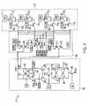
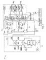
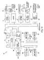
- FIG. 1illustrates a portion of a memory device 10 utilizing resistance variable memory elements as memory cells 12 0 , 12 1 .
- PCRAM elementsare used as the cells 12 0 , 12 1 .
- Each memory cell 12 0 , 12 1has a cell plate connected to a cell plate potential CPIN and is connected to a respective access transistor 14 0 , 14 1 .
- the first access transistor 14 0is connected between the first memory cell 12 0 and a first digit line DIGIT.
- the second access transistor 14 1is connected between the second memory cell 12 1 and a second digit line ⁇ overscore (DIGIT) ⁇ .
- the gates of the access transistors 14 0 , 14 1are connected to word lines WL 0 , WL 1 such that they receive row select signals R 0 , R 1 , respectively.
- the device 10also includes sensing circuitry 30 connected to the digit lines DIGIT, ⁇ overscore (DIGIT) ⁇ .
- the sensing circuitry 30includes an equilibration circuit 32 , two column select transistors 42 , 44 , a reference voltage circuit 50 , two isolating transistors 62 , 64 , a p-sense amplifier driver 78 , a p-sense amplifier circuit 70 , an n-sense amplifier driver 88 and an n-sense amplifier circuit 80 .
- the equilibration (EQ) circuit 32includes three EQ transistors 34 , 36 , 38 .
- the first EQ transistor 34is connected between the two digit lines DIGIT, ⁇ overscore (DIGIT) ⁇ .
- the second EQ transistor 36is connected between the first digit line DIGIT and the third EQ transistor 38 .
- the third EQ transistor 38is connected between the second digit line ⁇ overscore (DIGIT) ⁇ and the second EQ transistor 36 .
- the gate terminals of the three EQ transistors 34 , 36 , 38are connected to an equilibration gating line EQ.
- a bias voltage DVC 2is applied at the connection of the second and third EQ transistors 36 , 38 .
- All three of the EQ transistors 34 , 36 , 38are NMOS transistors.
- the equilibration circuit 32in response to the equilibration gating signal EQ, effectively equalizes the charges held by the digit lines DIGIT, ⁇ overscore (DIGIT) ⁇ after a read/write operation is completed and when the memory array is not active.
- the first column select transistor 42has its source and drain terminals connected between the first digit line DIGIT.
- the second column select transistor 44has its source and drain terminals connected between the second digit line ⁇ overscore (DIGIT) ⁇ .
- the gates of the column select transistors 42 , 44are connected to respective column select lines to receive a column select signal CSEL.
- the column select transistors 42 , 44are activated by the column select signal CSEL when it is desired to connect the remaining circuitry of the sensing circuitry 30 to the memory cells 12 0 , 12 1 (such as for example when it is time to write, erase or read the cells 12 0 , 12 1 ).
- the reference voltage circuit 50includes 4 reference voltage transistors 52 , 54 , 56 , 58 .
- the first reference voltage transistor 52is connected between the first digit line DIGIT and the second reference voltage transistor 54 .
- the second reference voltage transistor 54is connected between the first reference voltage transistor 52 and the second digit line ⁇ overscore (DIGIT) ⁇ .
- DVC 2is applied to the connection between the first and second reference voltage transistors 52 , 54 .
- the third reference voltage transistor 56is connected between the first digit line DIGIT and the fourth reference voltage transistor 58 .
- the fourth reference voltage transistor 58is connected between the third reference voltage transistor 56 and the second digit line ⁇ overscore (DIGIT) ⁇ .
- a reference voltage VREFis applied to the connection between the third and fourth reference voltage transistors 56 , 58 .
- the gate of the first reference voltage transistor 52is connected to the gate of the fourth reference voltage transistor 58 and to a first reference voltage signal REF E.
- the gate of the second reference voltage transistor 54is connected to the gate of the third reference voltage transistor 56 and to a second reference voltage signal REF O.
- the operation of the reference voltage circuit 50is explained below in more detail.
- the first isolating transistor 62is connected between the first digit line DIGIT and a first connection between the p-sense amplifier circuit 70 and the n-sense amplifier circuit 80 .
- the second isolating transistor 64is connected between the second digit line ⁇ overscore (DIGIT) ⁇ and a second connection between the p-sense amplifier circuit 70 and the n-sense amplifier circuit 80 .
- the gate terminals of the first and second isolating transistors 62 , 64are connected to an isolation gating signal SA ISO.
- the illustrated isolating transistors 62 , 64are NMOS transistors.
- the isolating transistors 62 , 64when activated by the isolation gating signal SA ISO, form isolation devices that effectively remove certain portions of the circuit 30 during addressing for a portion of a read and during a write and erase.
- the p-sense amplifier circuit 70includes two PMOS transistors 72 , 74 .
- the n-sense amplifier circuit 80includes two NMOS transistors 82 , 84 .
- the first PMOS transistor 72has its gate terminal connected to the second digit line ⁇ overscore (DIGIT) ⁇ and is connected between the first NMOS transistor 82 and the p-sense amplifier driver 78 .
- the second PMOS transistor 74has its gate terminal connected to the first digit line DIGIT and is connected between the second NMOS transistor 84 and driver 78 .
- the p-sense amplifier driver 78drives the p-sense amplifier 70 when a p-sense amplifier latching signal PL is applied to the gate of the driver 78 .
- the first NMOS transistor 82has its gate terminal connected to the second digit line ⁇ overscore (DIGIT) ⁇ and is connected between the n-sense amplifier driver 88 and the first PMOS transistor 72 .
- the second NMOS transistor 84has its gate terminal connected to the first digit line DIGIT and is connected between driver 88 and the second PMOS transistor 74 .
- the n-sense amplifier driver 88drives the n-sense amplifier 80 when an n-sense amplifier latching signal NL is applied to the gate of the driver 88 .
- Two write/erase circuits 92 0 , 92 1are respectively connected to the digit lines DIGIT, ⁇ overscore (DIGIT) ⁇ via the sensing circuitry 30 .
- the write/erase circuits 92 0 , 92 1apply a first programming voltage VPNS to the digit lines DIGIT, ⁇ overscore (DIGIT) ⁇ when the cells 12 0 or 12 1 are to be written to the high conductivity (i.e., lower resistance) state (as described above) depending on which row R 1 , R 0 is accessed.
- the write/erase circuits 92 0 , 92 1apply a second programming voltage VPPS, typically a reverse voltage (i.e., opposite bias) relative to the first programming voltage VPNS, to the digit lines DIGIT, ⁇ overscore (DIGIT) ⁇ when the cells 12 0 or 12 1 are to be written to the lower conductivity (i.e., higher resistance) state (as described above) depending on which row R 1 or R 0 is accessed.
- the appropriate column select transistors 42 , 44will also need to be activated during the write and erase operations.
- the first reference signal REF Eis generated, which causes the reference voltage circuit 50 to precharge the first digit line DIGIT to DVC 2 (via an activated first column select transistor 42 ).
- the reference voltage circuit 50precharges the second digit line ⁇ overscore (DIGIT) ⁇ to the reference voltage VREF. These precharged values will be applied to the digit lines and to the p-sense amplifier 70 and n-sense amplifier 80 (via activated isolation transistor 64 ).
- the current across the memory cell 12 0is sensed by p-sense amplifier 70 and n-sense amplifier 80 (via activated isolation transistor 62 ) and compared to the reference voltage VREF to determine the state of the memory cell 12 0 once the access transistor 14 0 is turned on.
- the second reference signal REF Ois generated, which causes the reference voltage circuit 50 to apply DVC 2 to the second digit line ⁇ overscore (DIGIT) ⁇ (via an activated second column select transistor 44 and access transistor 14 1 ).
- the reference voltage circuit 50applies the reference voltage VREF to the first digit line, DIGIT. Again, these precharged values will be applied to the digit lines and to the p-sense amplifier 70 and n-sense amplifier 80 (via activated isolation transistor 62 ).
- the current across the memory cell 12 1is sensed by p-sense amplifier 70 and n-sense amplifier 80 (via activated isolation transistor 64 ) and compared to the reference voltage VREF to determine the state of the memory cell 12 1 once the access transistor 141 is turned on.
- PCRAM cellssuch as e.g., cells 12 0 , 12 1
- Changes in the cell plate potential CPIN and the digit line programming voltages VPPS, VPNSallow an addressed cell to be written to or erased.
- the drawbackis that with different potentials for the cell plate and the equilibrated digit lines, non-addressed cells on the same word line may also become partially erased or written.
- FIG. 2illustrates a graph of sense time v. digit line voltage for the memory device 10 illustrated in FIG. 1 .
- Line 102represents the digit line voltage for a written cell.
- Line 104represents the digit line voltage for an erased cell. If DVC 2 is 1.0V (line 110 ) and CPIN is 1.2V (line 106 ), VREF is 1.1V (line 108 ).
- sensing differentialat the time the sense amplifiers are latched (e.g., at approximately 150 nS). Most likely, there is approximately a 60 mV differential when the cell is written and about a 40 mV differential when the cell is erased.
- sensing windowfor a resistance variable memory device such as e.g., a PCRAM memory device.
- sensing windowwithout causing the potential across the cell to be greater than approximately 200 mV.
- the inventionincreases the sensing window for a resistance variable memory device such as e.g., a PCRAM memory device.
- the inventionalso increases the sensing window without causing the potential across the cell to be greater than approximately 200 mV.
- the inventionalso provides a technique for writing to resistance variable memory cells while keeping the voltage across non-addressed cells at approximately 0V.
- the inventionalso provides a technique for sensing the state of resistance variable memory cells closer in time to when the cells are accessed (in comparison to typical sensing techniques).
- a resistance variable memory devicesuch as e.g., a PCRAM memory device, with either a 4T (transistor) or 2T memory cell configuration and either a dual cell plate or word line configuration.
- the deviceincludes additional circuitry configured to write or erase addressed cells while keeping the voltage across non-addressed cells at approximately 0V.
- the devicealso includes circuitry that reads the addressed cells in a manner that increases the sensing window without causing the potential across the cell to be greater than approximately 200 mV.
- the devicemay also sense the state of its addressed cells closer in time to when the cells are accessed, in comparison to typical sensing techniques.
- FIG. 1illustrates a portion of a memory device utilizing resistance variable memory elements as memory cells
- FIG. 2illustrates a graph of sense time v. digit line voltage for the memory device illustrated in FIG. 1 ;
- FIG. 3illustrates a graph of sense time v. digit line voltage for a memory device constructed in accordance with the present invention
- FIG. 4illustrates a portion of a memory device, utilizing resistance variable memory elements as memory cells, constructed in accordance with an exemplary embodiment of the invention
- FIG. 5illustrates a portion of the memory device illustrated in FIG. 4 ;
- FIGS. 6A , 6 B and 6 Care flowcharts illustrating exemplary methods of operating the device illustrated in FIGS. 4 and 5 ;
- FIG. 7illustrates a portion of a memory device, utilizing resistance variable memory elements as memory cells, constructed in accordance with another exemplary embodiment of the invention
- FIGS. 8A , 8 B and 8 Care flowcharts illustrating exemplary methods of operating the device illustrated in FIG. 7 ;
- FIG. 9illustrates a portion of a memory device, utilizing resistance variable memory elements as memory cells, constructed in accordance with yet another exemplary embodiment of the invention.
- FIG. 10illustrates a portion of the memory device illustrated in FIG. 9 ;
- FIGS. 11A , 11 B and 11 Care flowcharts illustrating exemplary methods of operating the device illustrated in FIGS. 9 and 10 ;
- FIG. 12shows a processor system incorporating at least one memory device constructed in accordance with an embodiment of the invention.
- FIG. 3depicts a graph of sense time v. digit line voltage for a memory device constructed in accordance with the invention.
- Line 122represents the digit line voltage for a written cell.
- Line 124represents the digit line voltage for an erased cell.
- the graphillustrates two cell plate voltages CPIN 1 (line 122 ) and CPIN 2 (line 124 ). The cell plate voltages CPIN 1 , CPIN 2 are discussed below in more detail.
- DVC 2is 1.0V (line 128 ), CPIN 1 is 1.2V (line 122 ), and CPIN 2 is 0.8V (line 130 ).
- the inventionalso increases the sensing window without causing the potential across the cell to be greater than approximately 200 mv.
- the inventionalso provides a technique for writing to resistance variable memory cells while keeping the voltage across non-addressed cells at approximately 0V.
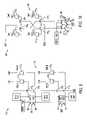
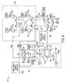
- FIG. 4illustrates a portion of a memory device 210 , utilizing resistance variable memory elements as memory cells 212 0 , 212 1 , 212 2 , 212 3 , constructed in accordance with an exemplary embodiment of the invention.
- PCRAM elementsare used as the cells 212 0 , 212 1 , 212 2 , 212 3 .
- the four memory cells 212 0 , 212 1 , 212 2 , 212 3are connected to the same word line WL via respective access transistors 214 0 , 214 1 , 214 2 , 214 3 .
- the first and third memory cells 212 0 , 212 2are connected to the first cell plate voltage CPIN 1 .
- the second and fourth memory cells 212 1 , 212 3are connected to the second cell plate voltage CPIN 2 .
- the first access transistor 214 0is connected between the first memory cell 212 0 (Cell A) and a right digit line DIGIT R.
- the second access transistor 214 1is connected between the second memory cell 212 1 (Cell B) and a left digit line DIGIT L.
- the third access transistor 214 2is connected between the third memory cell 212 2 ( ⁇ overscore (Cell A) ⁇ ) and a complementary right digit line ⁇ overscore (DIGIT R) ⁇ .
- the fourth access transistor 214 3is connected between the fourth memory cell 212 3 ( ⁇ overscore (Cell B) ⁇ ) and a complementary left digit line ⁇ overscore (DIGIT L) ⁇ .
- the gates of the access transistors 214 0 , 214 1 , 214 2 , 214 3are connected to the same word line WL such that they receive a row select signal R 0 at the same time.
- the memory cells 212 0 , 212 1 , 212 2 , 212 3 and access transistors 214 0 , 214 1 , 214 2 , 214 3make up one large 4T PCRAM cell 212 .
- the device 210also includes write/erase circuitry 290 connected between the digit lines DIGIT R, DIGIT L, ⁇ overscore (DIGIT R) ⁇ , ⁇ overscore (DIGIT L) ⁇ and the first and second digit lines DIGIT, ⁇ overscore (DIGIT) ⁇ .
- the first and second digit lines DIGIT, ⁇ overscore (DIGIT) ⁇are complementary to each other and can be referred to as the digit line DIGIT and complementary digit line ⁇ overscore (DIGIT) ⁇ .
- the write/erase circuitry 290also performs operations during a read operation and is discussed below in more detail.
- the device 210also includes sensing circuitry 230 connected to the first and second digit lines DIGIT, ⁇ overscore (DIGIT) ⁇ .
- the sensing circuitry 230includes an equilibration circuit 232 , two column select transistors 242 , 244 , two isolating transistors 256 , 258 , a p-sense amplifier driver 278 , a p-sense amplifier circuit 270 , an n-sense amplifier driver 288 and an n-sense amplifier circuit 280 .
- the equilibration (EQ) circuit 232includes three EQ transistors 234 , 236 , 238 .
- the first EQ transistor 234is connected between the two digit lines DIGIT, ⁇ overscore (DIGIT) ⁇ .
- the second EQ transistor 236is connected between the first digit line DIGIT and the third EQ transistor 238 .
- the third EQ transistor 238is connected between the second digit line ⁇ overscore (DIGIT) ⁇ and the second EQ transistor 236 .
- the gate terminals of the three EQ transistors 234 , 236 , 238are connected to an equilibration gating line EQ.
- a bias voltage DVC 2is applied at the connection of the second and third EQ transistors 236 , 238 .
- All three of the EQ transistors 234 , 236 , 238are NMOS transistors.
- the equilibration circuit 232in response to the equilibration gating signal EQ, effectively equalizes the charges held by the digit lines DIGIT, ⁇ overscore (DIGIT) ⁇ after a read/write operation is completed and when the memory array is not active.
- the first column select transistor 242has its source and drain terminals connected between the first digit line DIGIT.
- the second column select transistor 244has its source and drain terminals connected between the second digit line ⁇ overscore (DIGIT) ⁇ .
- the gates of the column select transistors 242 , 244are connected to respective column select lines to receive a column select signal CSEL.
- the column select transistors 242 , 244are activated by the column select signal CSEL when it is desired to connect the remaining circuitry of the sensing circuitry 230 to the memory cells 212 0 , 212 1 , 212 2 , 212 3 via circuit 290 and the access transistors 214 0 , 214 1 , 214 2 , 214 3 .
- the first isolating transistor 256is connected between the first digit line DIGIT and a first connection between the p-sense amplifier circuit 270 and the n-sense amplifier circuit 280 .
- the second isolating transistor 258is connected between the second digit line ⁇ overscore (DIGIT) ⁇ and a second connection between the p-sense amplifier circuit 270 and the n-sense amplifier circuit 280 .
- the gate terminals of the first and second isolating transistors 256 , 258are connected to an isolation gating signal SA ISO.
- the illustrated isolating transistors 256 , 258are NMOS transistors. The isolating transistors 256 , 258 , when activated by the isolation gating signal SA ISO, form isolation devices that effectively remove certain portions of the circuit 230 during addressing.
- the p-sense amplifier circuit 270includes two PMOS transistors 272 , 274 .
- the n-sense amplifier circuit 280includes two NMOS transistors 282 , 284 .
- the first PMOS transistor 272has its gate terminal connected to the second digit line ⁇ overscore (DIGIT) ⁇ and is connected between the first NMOS transistor 282 and the p-sense amplifier driver 278 .
- the second PMOS transistor 274has its gate terminal connected to the first digit line DIGIT and is connected between the second NMOS transistor 284 and driver 278 .
- the p-sense amplifier driver 278drives the p-sense amplifier 270 when a p-sense amplifier latching signal PL is applied to the gate of the driver 278 .
- the first NMOS transistor 282has its gate terminal connected to the second digit line ⁇ overscore (DIGIT) ⁇ and is connected between the n-sense amplifier driver 288 and the first PMOS transistor 272 .
- the second NMOS transistor 284has its gate terminal connected to the first digit line DIGIT and is connected between driver 288 and the second PMOS transistor 274 .
- the n-sense amplifier driver 288drives the n-sense amplifier 280 when an n-sense amplifier latching signal NL is applied to the gate of the driver 288 .
- the write/erase circuit 290contains four write/read transistors 300 , 302 , 312 , 314 and four programming column select transistors 304 , 306 , 308 , 310 .
- the first write/read transistor 300is connected between the second write/read transistor 302 and the right digit line DIGIT R.
- the second write/read transistor 302is connected between the first write/read transistor 300 and the left digit line DIGIT L.
- the connection between the first and second write/read transistors 300 , 302is connected to the first digit line DIGIT.
- the gates of the first and second write/read transistors 300 , 302are connected to a write/read control signal ⁇ overscore (WRITE) ⁇ READ.
- the third write/read transistor 312is connected between the fourth write/read transistor 314 and the complementary right digit line ⁇ overscore (DIGIT R) ⁇ .
- the fourth write/read transistor 314is connected between the second write/read transistor 312 and the complementary left digit line ⁇ overscore (DIGIT L) ⁇ .
- the connection between the third and fourth write/read transistors 312 , 314is connected to the complementary digit line ⁇ overscore (DIGIT) ⁇ .
- the gates of the third and fourth write/read transistors 312 , 314are connected to the write/read control signal ⁇ overscore (WRITE) ⁇ READ.
- the first programming column select transistor 304is connected between a first positive programming voltage VPPS 1 and a connection between the left digit line DIGIT L and the complementary right digit line ⁇ overscore (DIGIT R) ⁇ .
- the second programming column select transistor 306is connected between a first negative programming voltage VPNS 1 and a connection between the left digit line DIGIT L and the complementary right digit line ⁇ overscore (DIGIT R) ⁇ .
- the third programming column select transistor 308is connected between a second positive programming voltage VPPS 2 and a connection between the right digit line DIGIT R and the complementary left digit line ⁇ overscore (DIGIT L) ⁇ .
- the fourth programming column select transistor 310is connected between a second negative programming voltage VPNS 2 and a connection between the right digit line DIGIT R and the complementary left digit line ⁇ overscore (DIGIT L) ⁇ .
- the programming column select transistors 304 , 306 , 308 , 310are activated when it is time to write or erase the memory cells 212 0 , 212 1 , 212 2 , 212 3 .
- FIG. 5illustrates a portion of the memory device 210 in a more simplified manner.
- the FIG. 5 illustrationdoes not include the programming column select transistors 304 , 306 , 308 , 310 since it is presumed that they have been activated by the column select signal CSEL.
- the cell plate voltages CPIN 1 , CPIN 2are held at DVC 2 .
- the write/read control signal ⁇ overscore (WRITE) ⁇ READallows the right digit line DIGIT R and complementary left digit line ⁇ overscore (DIGIT L) ⁇ or the left digit line DIGIT and the complementary right digit line ⁇ overscore (DIGIT R) ⁇ to be accessed and programmed by the programming voltages VPPS 1 , VPPS 2 , VPNS 1 , VPNS 2 .
- All other non-accessed memory cells 212 0 , 212 1 , 212 2 , 212 3 associated with the accessed word line WLare not programmed since their top cell plate potential and their respective digit lines are held at DVC 2 . That is, the voltage across the non-addressed cells is approximately 0V.
- the first cell plate voltage CPIN 1is set to DVC 2 +200 mV and the second cell plate voltage is set to DVC 2 ⁇ 200 mV.
- the write/read control signal ⁇ overscore (WRITE) ⁇ READallows the right and left digit lines DIGIT R, DIGIT L to be connected to the sensing circuitry 230
- the accessed memory celleither pulls its digit line up to the first programming voltage CPIN 1 or down to the second programmed voltage CPIN 2 .
- cell 212 0Cell A
- cell 212 3⁇ overscore (Cell B) ⁇
- cell plate potentialse.g., CPIN 1 , CPIN 2
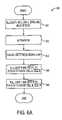
- the access transistors 214 0 , 214 1 , 214 2 , 214 3are activated by applying the row select signal R 0 (step 342 ).
- the write/read control signal ⁇ overscore (WRITE) ⁇ READis toggled low (step 343 ).
- the right digit line DIGIT R and the complementary left digit line ⁇ overscore (DIGIT L) ⁇are pulled to DVC 2 ⁇ 2V to write cell 212 0 (Cell A) and cell 212 3 ( ⁇ overscore (Cell B) ⁇ ) at step 344 .
- the left digit line DIGIT L and the complementary right digit line ⁇ overscore (DIGIT R) ⁇are pulled to DVC 2 +2V to erase cell 212 1 (Cell B) and cell 212 2 ( ⁇ overscore (Cell A) ⁇ ) at step 345 . This places the cell 212 in a high resistance state.
- cell 212 1 (Cell B) and cell 212 2 ( ⁇ overscore (Cell A) ⁇ )are written by writing the second digit line ⁇ overscore (DIGIT) ⁇ to a high state.
- all digit lines DIGIT R, DIGIT L, ⁇ overscore (DIGIT R) ⁇ , ⁇ overscore (DIGIT L) ⁇ and cell plate potentialsare held at DVC 2 (step 351 ).
- the access transistors 214 0 , 214 1 , 214 2 , 214 3are activated by applying the row select signal R 0 (step 352 ).
- the write/read control signal ⁇ overscore (WRITE) ⁇ READis toggled low (step 353 ).
- the left digit line DIGIT L and the complementary right digit line ⁇ overscore (DIGIT R) ⁇are pulled to DVC 2 ⁇ 2V to write cell 212 1 (Cell B) and cell 212 2 ⁇ overscore (Cell A) ⁇ at step 354 .
- the right digit line DIGIT R and the complementary left digit line ⁇ overscore (DIGIT L) ⁇are pulled to DVC 2 +2V to erase cell 212 0 (Cell A) and cell 212 3 ( ⁇ overscore (Cell B) ⁇ ) at step 355 . This places the cell 212 in a low resistance state.
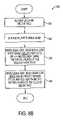
- an exemplary method 360 of operating the memory device 210is now described for a read operation.
- all digit lines DIGIT R, DIGIT L, ⁇ overscore (DIGIT R) ⁇ , ⁇ overscore (DIGIT L) ⁇are held at DVC 2 (step 361 ).
- the first cell plate voltage CPIN 1is set to DVC 2 +200 mV while the second cell plate voltage CPIN 2 is set to DVC 2 ⁇ 200 mV (step 362 ).
- the write/read control signal ⁇ overscore (WRITE) ⁇ READis toggled high (step 363 ) and the column can be accessed and sensed (step 364 ).
- WRITEwrite/read control signal
- FIG. 7illustrates a portion of a memory device 410 , utilizing resistance variable memory elements as memory cells 412 0 , 412 1 , 412 2 , 412 3 in a memory array 411 , constructed in accordance with another exemplary embodiment of the invention.
- PCRAM elementsare used as the cells 412 0 , 412 1 , 412 2 , 412 3 .
- the first two memory cells 412 0 , 412 1are connected to the first digit line DIGIT via access transistor 414 0 and contain different phase change material.
- the third and fourth memory cells 412 2 , 412 3are connected to the second line ⁇ overscore (DIGIT) ⁇ by access transistor 414 1 and contain different phase change material.
- the memory cells 412 0 , 412 1 , 412 2 , 412 3 and access transistors 414 0 , 414 1make up one large 2T PCRAM cell 412 .
- the gates of the access transistors 414 0 , 414 1are connected to the same word line WL such that they receive row select signal R 0 at the same time.
- the digit lines DIGIT, ⁇ overscore (DIGIT) ⁇are connected to sensing circuitry 230 , which is the same sensing circuitry described above with reference to FIG. 4 .
- the device 410also includes write/erase circuitry 490 connected to the cell plates of the memory cells 412 0 , 412 1 , 412 2 , 412 3 .
- the write/erase circuitry 490includes two write/erase circuits 492 0 , 492 1 and eight transistors 500 , 502 , 504 , 506 , 508 , 510 , 512 , 514 .
- the first transistor 500is connected between the second transistor 502 and the first cell plate potential CPIN 1 .
- the second transistor 502is connected between the first transistor 500 and the second write/erase circuit 492 1 .
- the cell plate of the first memory cell 412 0is connected to the connection between the first and second transistors 500 , 502 .
- the third transistor 504is connected between the fourth transistor 506 and the second cell plate potential CPIN 2 .
- the fourth transistor 506is connected between the third transistor 504 and the first write/erase circuit 492 0 .
- the cell plate of the second memory cell 412 1is connected to the connection between the third and fourth transistors 504 , 506 .
- the fifth transistor 508is connected between the sixth transistor 510 and CPIN 1 .
- the sixth transistor 510is connected between the fifth transistor 508 and the second write/erase circuit 492 1 .
- the cell plate of the third memory cell 412 2is connected to the connection between the fifth and sixth transistors 508 , 510 .
- the seventh transistor 512is connected between the eighth transistor 514 and CPIN 2 .
- the eighth transistor 514is connected between the seventh transistor 512 and the first write/erase circuit 492 0 .
- the cell plate of the fourth memory cell 412 3is connected to the connection between the seventh and eighth transistors 504 , 506 .
- the gates of the first, third, fifth and seventh transistors 500 , 504 , 508 , 512are connected to a read signal READ.
- the gates of the second, fourth, sixth and eighth transistors 502 , 506 , 510 , 514are connected to a write signal WRITE.
- the cell plate potentials CPIN 1 , CPIN 2are used to read and the write/erase circuits 492 0 , 492 1 are used to write or erase the memory cells 412 0 , 412 1 , 412 2 , 412 3 .
- a write signal WRITEcauses the cell plates to program the phase change resistance of the cells connected to the digit line DIGIT to one of the two voltages defined by the first write/erase circuit 492 0 (“Write Erase CIRCUIT 1 ”), for this example, DVC 2 +2V.
- the cell on the complementary digit line ⁇ overscore (DIGIT) ⁇is programmed to the opposite voltage defined by the second write/erase circuit 492 1 (“Write Erase CIRCUIT 2 ”), for this example, DVC 2 ⁇ 2V. All other non-accessed digit lines on the same word line are not programmed since their top cell plate and digital lines are at the same potential (i.e., DVC 2 ).
- the first cell plate voltage CPIN 1is set to DVC 2 +200 mV while the second cell plate voltage CPIN 2 is set to DVC 2 ⁇ 200 mV.
- the resistors within the memory cells 412 0 , 412 1 , 412 2 , 412 3are tied to their respective cell plate potentials.
- the programmed resistorse.g., memory cells 412 0 , 412 1 ) pull the digit line DIGIT up to CPIN 1 or down to CPIN 2 depending upon which cell was programmed.
- the cellse.g., memory cells 412 2 , 412 3
- cell 412 0Cell A
- cell 412 3⁇ overscore (Cell B) ⁇
- the digit lines DIGIT, ⁇ overscore (DIGIT) ⁇are held at DVC 2 (step 531 ).
- the access transistors 414 0 , 414 1are activated by applying the row select signal R 0 (step 532 ).
- the top cell plate for (Cell A) and ( ⁇ overscore (Cell B) ⁇ )are set to DVC 2 +2V through Write Erase Circuit 2 once the WRITE signal is given.
- the top cell plate for (Cell B) and ( ⁇ overscore (Cell A) ⁇ )are set to DVC 2 ⁇ 2V through Write Erase Circuit 1 once the WRITE signal is given.
- cell 412 1Cell B
- cell 412 2⁇ overscore (Cell A) ⁇
- the digit lines DIGIT, ⁇ overscore (DIGIT) ⁇are held at DVC 2 (step 541 ).
- the access transistors 414 0 , 414 1are activated by applying the row select signal R 0 (step 542 ).
- the first complementary top cell plates potentialsare set to DCV 2 +2V by the Write Erase CIRCUIT 1 once the WRITE signal is given, to write cell 412 1 (Cell B) and cell 412 2 ( ⁇ overscore (Cell A) ⁇ ) at step 543 .
- the first top cell plate potentialsare set to DCV 2 ⁇ 2V by the Write Erase CIRCUIT 2 once the WRITE signal is given, to erase cell 412 0 (Cell A) and cell 412 3 ( ⁇ overscore (Cell B) ⁇ ) at step 544 . This places the cell 412 in a low resistance state.
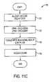
- an exemplary method 550 of operating the memory device 410is now described for a read operation.
- the digit lines DIGIT, ⁇ overscore (DIGIT) ⁇are held at DVC 2 (step 551 ).
- the first cell plate potential CPIN 1 and the complementary first cell plate potential CPIN 1are set to DVC 2 +200 mV at step 552 .
- the second cell plate potential CPIN 2 and the second complementary cell plate potential CPIN 2are set to DVC 2 ⁇ 2V at step 553 .
- the cell 412can now be sensed. As noted above, there will be a much larger sensing window as compared to the memory device 10 illustrated in FIGS. 1 and 2 .
- FIG. 9illustrates a portion of a memory device 610 , utilizing resistance variable memory elements as memory cells 612 0 , 612 1 , 612 2 , 612 3 , constructed in accordance with another exemplary embodiment of the invention.
- PCRAM elementsare used as the cells 612 0 , 612 1 , 612 2 , 612 3 .
- the first two memory cells 612 0 , 612 1are connected to the first digit line DIGIT via access transistors 614 0 , 614 1 .
- the other two memory cells 612 2 , 612 3are connected to the complementary digit line ⁇ overscore (DIGIT) ⁇ via access transistors 614 2 , 614 3 .
- DIGITcomplementary digit line ⁇ overscore
- the first and third memory cells 612 0 , 612 2have their cell plates connected to a first cell plate potential CPIN 1 .
- the second and fourth memory cells 612 1 , 612 3have their cell plates connected to a second cell plate potential CPIN 2 .
- the memory cells 612 0 , 612 1 , 612 2 , 612 3 and access transistors 614 0 , 6141 , 614 2 , 614 3make up one large 4T PCRAM cell 612 with a double word line WL r , WL 1 .
- the first access transistor 614 0is also connected to the first digit line DIGIT and one terminal of the second access transistor 614 1 .
- the second access transistor 614 1is also connected to the first digit line DIGIT and the first access transistor 614 0 .
- the third access transistor 614 2is connected to the fourth access transistor 614 3 and the complementary digit line ⁇ overscore (DIGIT) ⁇ .
- the gates of the first and fourth access transistors 614 0 , 614 3are connected to receive a right row select signal R 0 r from the right word line WL r via the write/read circuit 700 .
- the gates of the second and third access transistors 614 1 , 614 2are connected to receive a left row select signal R 0 1 from the left word line WL 1 via the write/read circuit 700 .
- the write/read circuit 700includes four write/read transistors 702 , 704 , 706 , 708 .
- the first write/read transistor 702is connected between the second write/read transistor 704 and a line 703 connected to the gates of the second and third access transistors 614 1 , 614 2 .
- the fourth write/read transistor 708is connected between the third write/read transistor 706 and line 703 .
- the second write/read transistor 704is connected between the first write/read transistor 702 and a line 705 connected to the gates of the first and fourth access transistors 614 0 , 614 3 .
- the third write/read transistor 706is connected between the fourth write/read transistor 708 and line 705 .
- the gates of the first and second write/read transistors 702 , 704are connected to receive a row select signal R 0 from a word line WL.
- the gates of the third and fourth write/read transistors 706 , 708are connected to the write/read control signal ⁇ overscore (WRITE) ⁇ READ.
- the digit lines DIGIT, ⁇ overscore (DIGIT) ⁇are connected to sensing circuitry 630 .
- the sensing circuitry 630includes an equilibration circuit 632 , two column select transistors 642 , 644 , two isolating transistors 656 , 658 , a p-sense amplifier driver 678 , a p-sense amplifier circuit 670 , an n-sense amplifier driver 688 and an n-sense amplifier circuit 680 .
- the equilibration (EQ) circuit 632includes three EQ transistors 634 , 636 , 638 .
- the first EQ transistor 634is connected between the two digit lines DIGIT, ⁇ overscore (DIGIT) ⁇ .
- the second EQ transistor 636is connected between the first digit line DIGIT and the third EQ transistor 638 .
- the third EQ transistor 638is connected between the second digit line ⁇ overscore (DIGIT) ⁇ and the second EQ transistor 636 .
- the gate terminals of the three EQ transistors 634 , 636 , 638are connected to an equilibration gating line EQ.
- a bias voltage DVC 2is applied at the connection of the second and third EQ transistors 636 , 638 .
- All three of the EQ transistors 634 , 636 , 638are NMOS transistors.
- the equilibration circuit 632in response to the equilibration gating signal EQ effectively equalizes the charges held by the digit lines DIGIT, ⁇ overscore (DIGIT) ⁇ after a read/write operation is completed and when the memory array is not active.
- the first column select transistor 642has its source and drain terminals connected between the first digit line DIGIT.
- the second column select transistor 644has its source and drain terminals connected between the second digit line ⁇ overscore (DIGIT) ⁇ .
- the gates of the column select transistors 642 , 644are connected to respective column select lines to receive a column select signal CSEL.
- the column select transistors 642 , 644are activated by the column select signal CSEL when it is desired to connect the remaining circuitry 630 to the memory cells 612 0 , 612 1 , 612 2 , 612 3 .
- the first isolating transistor 656is connected between the first digit line DIGIT and a first connection between the p-sense amplifier circuit 670 and the n-sense amplifier circuit 680 .
- the second isolating transistor 658is connected between the second digit line ⁇ overscore (DIGIT) ⁇ and a second connection between the p-sense amplifier circuit 670 and the n-sense amplifier circuit 680 .
- the gate terminals of the first and second isolating transistors 656 , 658are connected to an isolation gating signal SA ISO.
- the illustrated isolating transistors 656 , 658are NMOS transistors. The isolating transistors 656 , 658 , when activated by the isolation gating signal SA ISO, form isolation devices that effectively remove certain portions of the circuit 630 during addressing.
- the p-sense amplifier circuit 670includes two PMOS transistors 672 , 674 .
- the n-sense amplifier circuit 680includes two NMOS transistors 682 , 684 .
- the first PMOS transistor 672has its gate terminal connected to the second digit line ⁇ overscore (DIGIT) ⁇ and is connected between the first NMOS transistor 682 and the p-sense amplifier driver 678 .
- the second PMOS transistor 674has its gate terminal connected to the first digit line DIGIT and is connected between the second NMOS transistor 684 and driver 678 .
- the p-sense amplifier driver 678drives the p-sense amplifier 670 when a p-sense amplifier latching signal PL is applied to the gate of the driver 678 .
- the first NMOS transistor 682has its gate terminal connected to the second digit line ⁇ overscore (DIGIT) ⁇ and is connected between the n-sense amplifier driver 688 and the first PMOS transistor 672 .
- the second NMOS transistor 684has its gate terminal connected to the first digit line DIGIT and is connected between driver 688 and the second PMOS transistor 674 .
- the n-sense amplifier driver 688drives the n-sense amplifier 680 when an n-sense amplifier latching signal NL is applied to the gate of the driver 688 .
- the device 610also includes write/erase circuitry 692 0 , 692 1 connected to sensing circuitry 630 .
- the first write/erase circuit 692 0is connected to the first digit line DIGIT when the first column select transistor 642 is activated by the column select signal CSEL.
- the second write/erase circuit 692 1is connected to the complementary digit line ⁇ overscore (DIGIT) ⁇ when the second column select transistor 644 is activated by the column select signal CSEL.
- the write/erase circuitry 692 0 , 692 1also performs operations during a read operation and is discussed below in more detail.
- FIG. 10illustrates a portion of the memory device 610 illustrated in FIG. 9 .
- the FIG. 10 illustrationdoes not include the sensing circuitry 630 or the write/erase circuits 692 0 , 692 1 for clarity purposes.
- the cell platesare held at DVC 2 (via CPIN 1 and CPIN 2 ) and the write/read control signal ⁇ overscore (WRITE) ⁇ READ allows the left or right word lines WL 1 , WL r to access complimentary cells, which are programmed with the VPPS or VPNS potentials that are applied to the digit lines DIGIT, ⁇ overscore (DIGIT) ⁇ . All other non-accessed memory cells 612 0 , 612 1 , 612 2 , 612 3 associated with the accessed word line are not programmed since their top cell plate potential and their respective digit lines are held at DVC 2 . That is, the voltage across the non-addressed cells is approximately 0V.
- the first cell plate potential CPIN 1is set to DVC 2 +200 mV and the second cell plate potential CPIN 2 is set to DVC 2 ⁇ 200 mV.
- the write/read control signal ⁇ overscore (WRITE) ⁇ READis toggled high to turn on the left and right word lines WL 1 , WL r .
- the programmed cellcan pull its digit line up to CPIN 1 or down to CPIN 2 depending upon which word line WL 1 , WL r was used to program the cell.
- cell 612 0Cell A
- cell 612 3⁇ overscore (Cell B) ⁇
- the digit lines DIGIT, ⁇ overscore (DIGIT) ⁇ and the cell plate potentials CPIN 1 , CPIN 2are held at DVC 2 (step 731 ).
- the write/read control signal ⁇ overscore (WRITE) ⁇ READis toggled high at step 732 .
- the row select signal R 0is generate (step 733 ).
- the addressed cellsare erased by pulling the digit lines DIGIT, ⁇ overscore (DIGIT) ⁇ to DVC 2 +2V at step 734 .
- the digit lines DIGIT, ⁇ overscore (DIGIT) ⁇are returned to DVC 2 at step 735 .
- the write/read control signal ⁇ overscore (WRITE) ⁇ READis toggled low while the right word line WL r is toggled high and the left word line WL 1 is toggled low (step 736 ).
- the digit lines DIGIT, ⁇ overscore (DIGIT) ⁇are pulled to DVC 2 ⁇ 2V to write cell 612 0 (Cell A) and cell 612 3 ( ⁇ overscore (Cell B) ⁇ ) at step 737 . This places the cell 612 in a high resistance state.
- cell 612 1Cell B
- cell 612 2⁇ overscore (Cell A) ⁇
- the digit lines DIGIT, ⁇ overscore (DIGIT) ⁇ and the cell plate potentials CPIN 1 , CPIN 2are held at DVC 2 (step 741 ).
- the write/read control signal ⁇ overscore (WRITE) ⁇ READis toggled high at step 742 .
- the row select signal R 0is generate (step 743 ).
- the addressed cellsare erased by pulling the digit lines DIGIT, ⁇ overscore (DIGIT) ⁇ to DVC 2 +2V at step 744 .
- the digit lines DIGIT, ⁇ overscore (DIGIT) ⁇are returned to DVC 2 at step 745 .
- the write/read control signal ⁇ overscore (WRITE) ⁇ READis toggled low while the right word line WL r is toggled low and the left word line WL 1 is toggled high (step 746 ).
- the digit lines DIGIT, ⁇ overscore (DIGIT) ⁇are pulled to DVC 2 ⁇ 2V to write cell 612 1 (Cell B) and cell 612 2 ( ⁇ overscore (Cell A) ⁇ ) are written to a high state at step 747 . This places the cell 612 in a low resistance state.
- the digit lines DIGIT, ⁇ overscore (DIGIT) ⁇are held at DVC 2 (step 751 ).
- the first cell plate potential CPIN 1is set to DVC 2 +200 mV and the second cell plate potential CPIN 2 is set to DVC 2 ⁇ 2V at step 752 .
- the write/read control signal ⁇ overscore (WRITE) ⁇ READis toggled high while the right and left word lines WL r , WL 1 are toggled low.
- the columnis then accessed and the sensing of the digit lines DIGIT, ⁇ overscore (DIGIT) ⁇ occurs (step 754 ). As noted above, there will be a much larger sensing window as compared to the memory device 10 illustrated in FIGS. 1 and 2 .
- FIG. 12shows a processor system 900 that may utilize a memory device 100 incorporating one of the embodiments of the invention (i.e., deice 210 , 410 , 610 of FIGS. 4 , 7 , 9 ), in accordance with the invention.
- the processing system 900includes one or more processors 901 coupled to a local bus 904 .
- a memory controller 902 and a primary bus bridge 903are also coupled the local bus 904 .
- the processing system 900may include multiple memory controllers 902 and/or multiple primary bus bridges 903 .
- the memory controller 902 and the primary bus bridge 903may be integrated as a single device 906 .
- the memory controller 902is also coupled to one or more memory buses 907 .
- Each memory bus 907accepts memory components 908 which include at least one memory device 100 of the present invention.
- the memory components 908may be a memory card or a memory module. Examples of memory modules include single inline memory modules (SIMMs) and dual inline memory modules (DIMMs).
- the memory components 908may include one or more additional devices 909 .
- the additional device 909might be a configuration memory, such as a serial presence detect (SPD) memory.
- the memory controller 902may also be coupled to a cache memory 905 .
- the cache memory 905may be the only cache memory in the processing system.
- processors 901may also include cache memories, which may form a cache hierarchy with cache memory 905 .
- the processing system 900includes peripherals or controllers which are bus masters or which support direct memory access (DMA), the memory controller 902 may implement a cache coherency protocol. If the memory controller 902 is coupled to a plurality of memory buses 907 , each memory bus 907 may be operated in parallel, or different address ranges may be mapped to different memory buses 907 .
- DMAdirect memory access
- the primary bus bridge 903is coupled to at least one peripheral bus 910 .
- Various devicessuch as peripherals or additional bus bridges may be coupled to the peripheral bus 910 . These devices may include a storage controller 911 , a miscellaneous I/O device 914 , a secondary bus bridge 915 , a multimedia processor 918 , and a legacy device interface 920 .
- the primary bus bridge 903may also coupled to one or more special purpose high speed ports 922 . In a personal computer, for example, the special purpose port might be the Accelerated Graphics Port (AGP), used to couple a high performance video card to the processing system 900 .
- AGPAccelerated Graphics Port
- the storage controller 911couples one or more storage devices 913 , via a storage bus 912 , to the peripheral bus 910 .
- the storage controller 911may be a SCSI controller and storage devices 913 may be SCSI discs.
- the I/O device 914may be any sort of peripheral.
- the I/O device 914may be a local area network interface, such as an Ethernet card.
- the secondary bus bridge 915may be used to interface additional devices via another bus to the processing system.
- the secondary bus bridge 915may be an universal serial port (USB) controller used to couple USB devices 917 via to the processing system 900 .
- USBuniversal serial port
- the multimedia processor 918may be a sound card, a video capture card, or any other type of media interface, which may also be coupled to one additional devices such as speakers 919 .
- the legacy device interface 920is used to couple legacy devices 921 , for example, older styled keyboards and mice, to the processing system 900 .
- the processing system 900 illustrated in FIG. 12is only an exemplary processing system that may use the memory devices of the invention. While FIG. 12 illustrates a processing architecture especially suitable for a general purpose computer, such as a personal computer or a workstation, it should be recognized that well known modifications can be made to configure the processing system 900 to become more suitable for use in a variety of applications. For example, many electronic devices which require processing may be implemented using a simpler architecture which relies on a CPU 901 coupled to memory components 908 and/or memory devices 100 .
- These electronic devicesmay include, but are not limited to audio/video processors and recorders, gaming consoles, digital television sets, wired or wireless telephones, navigation devices (including system based on the global positioning system (GPS) and/or inertial navigation), and digital cameras and/or recorders.
- the modificationsmay include, for example, elimination of unnecessary components, addition of specialized devices or circuits, and/or integration of a plurality of devices.
- a method of manufacturing a memory deviceincludes the acts of providing an array of memory cells, each cell being connected to first and second digit lines, each cell comprising a plurality of resistance variable memory elements and a plurality of access; and providing sensing circuitry connected to the first and second digit lines, said sensing circuitry sensing the state of an addressed memory cell by changing a cell plate potential of the memory elements within the cell and sensing the difference between the first and second digit lines connected to the addressed cell.
Landscapes
- Chemical & Material Sciences (AREA)
- Crystallography & Structural Chemistry (AREA)
- Semiconductor Memories (AREA)
Abstract
Description
Claims (58)
Priority Applications (2)
| Application Number | Priority Date | Filing Date | Title |
|---|---|---|---|
| US10/931,129US7151688B2 (en) | 2004-09-01 | 2004-09-01 | Sensing of resistance variable memory devices |
| US11/473,308US7190608B2 (en) | 2004-09-01 | 2006-06-23 | Sensing of resistance variable memory devices |
Applications Claiming Priority (1)
| Application Number | Priority Date | Filing Date | Title |
|---|---|---|---|
| US10/931,129US7151688B2 (en) | 2004-09-01 | 2004-09-01 | Sensing of resistance variable memory devices |
Related Child Applications (1)
| Application Number | Title | Priority Date | Filing Date |
|---|---|---|---|
| US11/473,308ContinuationUS7190608B2 (en) | 2004-09-01 | 2006-06-23 | Sensing of resistance variable memory devices |
Publications (2)
| Publication Number | Publication Date |
|---|---|
| US20060044906A1 US20060044906A1 (en) | 2006-03-02 |
| US7151688B2true US7151688B2 (en) | 2006-12-19 |
Family
ID=35942841
Family Applications (2)
| Application Number | Title | Priority Date | Filing Date |
|---|---|---|---|
| US10/931,129Expired - LifetimeUS7151688B2 (en) | 2004-09-01 | 2004-09-01 | Sensing of resistance variable memory devices |
| US11/473,308Expired - LifetimeUS7190608B2 (en) | 2004-09-01 | 2006-06-23 | Sensing of resistance variable memory devices |
Family Applications After (1)
| Application Number | Title | Priority Date | Filing Date |
|---|---|---|---|
| US11/473,308Expired - LifetimeUS7190608B2 (en) | 2004-09-01 | 2006-06-23 | Sensing of resistance variable memory devices |
Country Status (1)
| Country | Link |
|---|---|
| US (2) | US7151688B2 (en) |
Cited By (6)
| Publication number | Priority date | Publication date | Assignee | Title |
|---|---|---|---|---|
| US7366045B2 (en)* | 2005-05-16 | 2008-04-29 | Micron Technology, Inc. | Power circuits for reducing a number of power supply voltage taps required for sensing a resistive memory |
| US20090237984A1 (en)* | 2008-03-21 | 2009-09-24 | Micron Technology, Inc. | Memory cell |
| US20100032732A1 (en)* | 2008-08-06 | 2010-02-11 | International Business Machines Corporation | Electrical antifuse having a multi-thickness dielectric layer |
| US20110019456A1 (en)* | 2009-07-24 | 2011-01-27 | Macronix International Co., Ltd. | Sense amplifier with shielding circuit |
| US9361975B2 (en) | 2013-03-11 | 2016-06-07 | Adesto Technologies Corporation | Sensing data in resistive switching memory devices |
| US20190362790A1 (en)* | 2016-03-16 | 2019-11-28 | Micron Technology, Inc. | Feram-dram hybrid memory |
Families Citing this family (2)
| Publication number | Priority date | Publication date | Assignee | Title |
|---|---|---|---|---|
| DE102004047638B4 (en)* | 2004-09-30 | 2011-12-01 | Qimonda Ag | Non-volatile memory cell |
| US7881100B2 (en)* | 2008-04-08 | 2011-02-01 | Micron Technology, Inc. | State machine sensing of memory cells |
Citations (184)
| Publication number | Priority date | Publication date | Assignee | Title |
|---|---|---|---|---|
| US3271591A (en) | 1963-09-20 | 1966-09-06 | Energy Conversion Devices Inc | Symmetrical current controlling device |
| US3622319A (en) | 1966-10-20 | 1971-11-23 | Western Electric Co | Nonreflecting photomasks and methods of making same |
| US3743847A (en) | 1971-06-01 | 1973-07-03 | Motorola Inc | Amorphous silicon film as a uv filter |
| US3961314A (en) | 1974-03-05 | 1976-06-01 | Energy Conversion Devices, Inc. | Structure and method for producing an image |
| US3966317A (en) | 1974-04-08 | 1976-06-29 | Energy Conversion Devices, Inc. | Dry process production of archival microform records from hard copy |
| US3983542A (en) | 1970-08-13 | 1976-09-28 | Energy Conversion Devices, Inc. | Method and apparatus for recording information |
| US4177474A (en) | 1977-05-18 | 1979-12-04 | Energy Conversion Devices, Inc. | High temperature amorphous semiconductor member and method of making the same |
| US4267261A (en) | 1971-07-15 | 1981-05-12 | Energy Conversion Devices, Inc. | Method for full format imaging |
| US4269935A (en) | 1979-07-13 | 1981-05-26 | Ionomet Company, Inc. | Process of doping silver image in chalcogenide layer |
| JPS56126916A (en) | 1980-03-10 | 1981-10-05 | Nippon Telegr & Teleph Corp <Ntt> | Manufacture of semiconductor device |
| US4312938A (en) | 1979-07-06 | 1982-01-26 | Drexler Technology Corporation | Method for making a broadband reflective laser recording and data storage medium with absorptive underlayer |
| US4316946A (en) | 1979-12-03 | 1982-02-23 | Ionomet Company, Inc. | Surface sensitized chalcogenide product and process for making and using the same |
| US4320191A (en) | 1978-11-07 | 1982-03-16 | Nippon Telegraph & Telephone Public Corporation | Pattern-forming process |
| US4405710A (en) | 1981-06-22 | 1983-09-20 | Cornell Research Foundation, Inc. | Ion beam exposure of (g-Gex -Se1-x) inorganic resists |
| US4419421A (en) | 1979-01-15 | 1983-12-06 | Max-Planck-Gesellschaft Zur Forderung Der Wissenschaften E.V. | Ion conductor material |
| US4499557A (en) | 1980-10-28 | 1985-02-12 | Energy Conversion Devices, Inc. | Programmable cell for use in programmable electronic arrays |
| US4597162A (en) | 1983-01-18 | 1986-07-01 | Energy Conversion Devices, Inc. | Method for making, parallel preprogramming or field programming of electronic matrix arrays |
| US4608296A (en) | 1983-12-06 | 1986-08-26 | Energy Conversion Devices, Inc. | Superconducting films and devices exhibiting AC to DC conversion |
| US4637895A (en) | 1985-04-01 | 1987-01-20 | Energy Conversion Devices, Inc. | Gas mixtures for the vapor deposition of semiconductor material |
| US4646266A (en) | 1984-09-28 | 1987-02-24 | Energy Conversion Devices, Inc. | Programmable semiconductor structures and methods for using the same |
| US4664939A (en) | 1985-04-01 | 1987-05-12 | Energy Conversion Devices, Inc. | Vertical semiconductor processor |
| US4668968A (en) | 1984-05-14 | 1987-05-26 | Energy Conversion Devices, Inc. | Integrated circuit compatible thin film field effect transistor and method of making same |
| US4670763A (en) | 1984-05-14 | 1987-06-02 | Energy Conversion Devices, Inc. | Thin film field effect transistor |
| US4671618A (en) | 1986-05-22 | 1987-06-09 | Wu Bao Gang | Liquid crystalline-plastic material having submillisecond switch times and extended memory |
| US4673957A (en) | 1984-05-14 | 1987-06-16 | Energy Conversion Devices, Inc. | Integrated circuit compatible thin film field effect transistor and method of making same |
| US4678679A (en) | 1984-06-25 | 1987-07-07 | Energy Conversion Devices, Inc. | Continuous deposition of activated process gases |
| US4710899A (en) | 1985-06-10 | 1987-12-01 | Energy Conversion Devices, Inc. | Data storage medium incorporating a transition metal for increased switching speed |
| US4728406A (en) | 1986-08-18 | 1988-03-01 | Energy Conversion Devices, Inc. | Method for plasma - coating a semiconductor body |
| US4737379A (en) | 1982-09-24 | 1988-04-12 | Energy Conversion Devices, Inc. | Plasma deposited coatings, and low temperature plasma method of making same |
| US4766471A (en) | 1986-01-23 | 1988-08-23 | Energy Conversion Devices, Inc. | Thin film electro-optical devices |
| US4769338A (en) | 1984-05-14 | 1988-09-06 | Energy Conversion Devices, Inc. | Thin film field effect transistor and method of making same |
| US4775425A (en) | 1987-07-27 | 1988-10-04 | Energy Conversion Devices, Inc. | P and n-type microcrystalline semiconductor alloy material including band gap widening elements, devices utilizing same |
| US4788594A (en) | 1986-10-15 | 1988-11-29 | Energy Conversion Devices, Inc. | Solid state electronic camera including thin film matrix of photosensors |
| US4795657A (en) | 1984-04-13 | 1989-01-03 | Energy Conversion Devices, Inc. | Method of fabricating a programmable array |
| US4800526A (en) | 1987-05-08 | 1989-01-24 | Gaf Corporation | Memory element for information storage and retrieval system and associated process |
| US4809044A (en) | 1986-08-22 | 1989-02-28 | Energy Conversion Devices, Inc. | Thin film overvoltage protection devices |
| US4818717A (en) | 1986-06-27 | 1989-04-04 | Energy Conversion Devices, Inc. | Method for making electronic matrix arrays |
| US4843443A (en) | 1984-05-14 | 1989-06-27 | Energy Conversion Devices, Inc. | Thin film field effect transistor and method of making same |
| US4847674A (en) | 1987-03-10 | 1989-07-11 | Advanced Micro Devices, Inc. | High speed interconnect system with refractory non-dogbone contacts and an active electromigration suppression mechanism |
| US4853785A (en) | 1986-10-15 | 1989-08-01 | Energy Conversion Devices, Inc. | Electronic camera including electronic signal storage cartridge |
| US4891330A (en) | 1987-07-27 | 1990-01-02 | Energy Conversion Devices, Inc. | Method of fabricating n-type and p-type microcrystalline semiconductor alloy material including band gap widening elements |
| US5128099A (en) | 1991-02-15 | 1992-07-07 | Energy Conversion Devices, Inc. | Congruent state changeable optical memory material and device |
| US5159661A (en) | 1990-10-05 | 1992-10-27 | Energy Conversion Devices, Inc. | Vertically interconnected parallel distributed processor |
| US5166758A (en) | 1991-01-18 | 1992-11-24 | Energy Conversion Devices, Inc. | Electrically erasable phase change memory |
| US5177567A (en) | 1991-07-19 | 1993-01-05 | Energy Conversion Devices, Inc. | Thin-film structure for chalcogenide electrical switching devices and process therefor |
| US5219788A (en) | 1991-02-25 | 1993-06-15 | Ibm Corporation | Bilayer metallization cap for photolithography |
| US5238862A (en) | 1992-03-18 | 1993-08-24 | Micron Technology, Inc. | Method of forming a stacked capacitor with striated electrode |
| US5272359A (en) | 1988-04-07 | 1993-12-21 | California Institute Of Technology | Reversible non-volatile switch based on a TCNQ charge transfer complex |
| US5296716A (en) | 1991-01-18 | 1994-03-22 | Energy Conversion Devices, Inc. | Electrically erasable, directly overwritable, multibit single cell memory elements and arrays fabricated therefrom |
| US5315131A (en) | 1990-11-22 | 1994-05-24 | Matsushita Electric Industrial Co., Ltd. | Electrically reprogrammable nonvolatile memory device |
| US5314772A (en) | 1990-10-09 | 1994-05-24 | Arizona Board Of Regents | High resolution, multi-layer resist for microlithography and method therefor |
| US5335219A (en) | 1991-01-18 | 1994-08-02 | Ovshinsky Stanford R | Homogeneous composition of microcrystalline semiconductor material, semiconductor devices and directly overwritable memory elements fabricated therefrom, and arrays fabricated from the memory elements |
| US5341328A (en) | 1991-01-18 | 1994-08-23 | Energy Conversion Devices, Inc. | Electrically erasable memory elements having reduced switching current requirements and increased write/erase cycle life |
| US5350484A (en) | 1992-09-08 | 1994-09-27 | Intel Corporation | Method for the anisotropic etching of metal films in the fabrication of interconnects |
| US5359205A (en) | 1991-11-07 | 1994-10-25 | Energy Conversion Devices, Inc. | Electrically erasable memory elements characterized by reduced current and improved thermal stability |
| US5360981A (en) | 1989-05-11 | 1994-11-01 | British Telecommunications Public Limited Company | Amorphous silicon memory |
| US5406509A (en) | 1991-01-18 | 1995-04-11 | Energy Conversion Devices, Inc. | Electrically erasable, directly overwritable, multibit single cell memory elements and arrays fabricated therefrom |
| US5414271A (en) | 1991-01-18 | 1995-05-09 | Energy Conversion Devices, Inc. | Electrically erasable memory elements having improved set resistance stability |
| US5500532A (en) | 1994-08-18 | 1996-03-19 | Arizona Board Of Regents | Personal electronic dosimeter |
| US5512328A (en) | 1992-08-07 | 1996-04-30 | Hitachi, Ltd. | Method for forming a pattern and forming a thin film used in pattern formation |
| US5512773A (en) | 1993-12-23 | 1996-04-30 | U.S. Philips Corporation | Switching element with memory provided with Schottky tunnelling barrier |
| US5534711A (en) | 1991-01-18 | 1996-07-09 | Energy Conversion Devices, Inc. | Electrically erasable, directly overwritable, multibit single cell memory elements and arrays fabricated therefrom |
| US5534712A (en) | 1991-01-18 | 1996-07-09 | Energy Conversion Devices, Inc. | Electrically erasable memory elements characterized by reduced current and improved thermal stability |
| US5536947A (en) | 1991-01-18 | 1996-07-16 | Energy Conversion Devices, Inc. | Electrically erasable, directly overwritable, multibit single cell memory element and arrays fabricated therefrom |
| US5543737A (en) | 1995-02-10 | 1996-08-06 | Energy Conversion Devices, Inc. | Logical operation circuit employing two-terminal chalcogenide switches |
| US5591501A (en) | 1995-12-20 | 1997-01-07 | Energy Conversion Devices, Inc. | Optical recording medium having a plurality of discrete phase change data recording points |
| US5596522A (en) | 1991-01-18 | 1997-01-21 | Energy Conversion Devices, Inc. | Homogeneous compositions of microcrystalline semiconductor material, semiconductor devices and directly overwritable memory elements fabricated therefrom, and arrays fabricated from the memory elements |
| US5687112A (en) | 1996-04-19 | 1997-11-11 | Energy Conversion Devices, Inc. | Multibit single cell memory element having tapered contact |
| US5694054A (en) | 1995-11-28 | 1997-12-02 | Energy Conversion Devices, Inc. | Integrated drivers for flat panel displays employing chalcogenide logic elements |
| US5714768A (en) | 1995-10-24 | 1998-02-03 | Energy Conversion Devices, Inc. | Second-layer phase change memory array on top of a logic device |
| US5726083A (en) | 1994-11-29 | 1998-03-10 | Nec Corporation | Process of fabricating dynamic random access memory device having storage capacitor low in contact resistance and small in leakage current through tantalum oxide film |
| US5751012A (en) | 1995-06-07 | 1998-05-12 | Micron Technology, Inc. | Polysilicon pillar diode for use in a non-volatile memory cell |
| US5761115A (en) | 1996-05-30 | 1998-06-02 | Axon Technologies Corporation | Programmable metallization cell structure and method of making same |
| US5789277A (en) | 1996-07-22 | 1998-08-04 | Micron Technology, Inc. | Method of making chalogenide memory device |
| US5814527A (en) | 1996-07-22 | 1998-09-29 | Micron Technology, Inc. | Method of making small pores defined by a disposable internal spacer for use in chalcogenide memories |
| US5818749A (en) | 1993-08-20 | 1998-10-06 | Micron Technology, Inc. | Integrated circuit memory device |
| US5825046A (en) | 1996-10-28 | 1998-10-20 | Energy Conversion Devices, Inc. | Composite memory material comprising a mixture of phase-change memory material and dielectric material |
| US5841150A (en) | 1995-06-07 | 1998-11-24 | Micron Technology, Inc. | Stack/trench diode for use with a muti-state material in a non-volatile memory cell |
| US5846889A (en) | 1997-03-14 | 1998-12-08 | The United States Of America As Represented By The Secretary Of The Navy | Infrared transparent selenide glasses |
| US5851882A (en) | 1996-05-06 | 1998-12-22 | Micron Technology, Inc. | ZPROM manufacture and design and methods for forming thin structures using spacers as an etching mask |
| US5869843A (en) | 1995-06-07 | 1999-02-09 | Micron Technology, Inc. | Memory array having a multi-state element and method for forming such array or cells thereof |
| WO1999028914A2 (en) | 1997-12-04 | 1999-06-10 | Axon Technologies Corporation | Programmable sub-surface aggregating metallization structure and method of making same |
| US5912839A (en) | 1998-06-23 | 1999-06-15 | Energy Conversion Devices, Inc. | Universal memory element and method of programming same |
| US5920788A (en) | 1995-06-07 | 1999-07-06 | Micron Technology, Inc. | Chalcogenide memory cell with a plurality of chalcogenide electrodes |
| US5933365A (en) | 1997-06-19 | 1999-08-03 | Energy Conversion Devices, Inc. | Memory element with energy control mechanism |
| US5998066A (en) | 1997-05-16 | 1999-12-07 | Aerial Imaging Corporation | Gray scale mask and depth pattern transfer technique using inorganic chalcogenide glass |
| US6011757A (en) | 1998-01-27 | 2000-01-04 | Ovshinsky; Stanford R. | Optical recording media having increased erasability |
| US6031287A (en) | 1997-06-18 | 2000-02-29 | Micron Technology, Inc. | Contact structure and memory element incorporating the same |
| US6072716A (en) | 1999-04-14 | 2000-06-06 | Massachusetts Institute Of Technology | Memory structures and methods of making same |
| US6087674A (en) | 1996-10-28 | 2000-07-11 | Energy Conversion Devices, Inc. | Memory element with memory material comprising phase-change material and dielectric material |
| US6117720A (en) | 1995-06-07 | 2000-09-12 | Micron Technology, Inc. | Method of making an integrated circuit electrode having a reduced contact area |
| US6141241A (en) | 1998-06-23 | 2000-10-31 | Energy Conversion Devices, Inc. | Universal memory element with systems employing same and apparatus and method for reading, writing and programming same |
| US6143604A (en) | 1999-06-04 | 2000-11-07 | Taiwan Semiconductor Manufacturing Company | Method for fabricating small-size two-step contacts for word-line strapping on dynamic random access memory (DRAM) |
| US6177338B1 (en) | 1999-02-08 | 2001-01-23 | Taiwan Semiconductor Manufacturing Company | Two step barrier process |
| US6236059B1 (en) | 1996-08-22 | 2001-05-22 | Micron Technology, Inc. | Memory cell incorporating a chalcogenide element and method of making same |
| US6297170B1 (en) | 1998-06-23 | 2001-10-02 | Vlsi Technology, Inc. | Sacrificial multilayer anti-reflective coating for mos gate formation |
| US6300684B1 (en) | 1995-06-07 | 2001-10-09 | Micron Technology, Inc. | Method for fabricating an array of ultra-small pores for chalcogenide memory cells |
| WO2000048196A9 (en) | 1999-02-11 | 2001-11-01 | Univ Arizona | Programmable microelectronic devices and methods of forming and programming same |
| US6329606B1 (en) | 1996-04-24 | 2001-12-11 | Amkor Technology, Inc. | Grid array assembly of circuit boards with singulation grooves |
| US20020000666A1 (en) | 1998-08-31 | 2002-01-03 | Michael N. Kozicki | Self-repairing interconnections for electrical circuits |
| US6339544B1 (en) | 2000-09-29 | 2002-01-15 | Intel Corporation | Method to enhance performance of thermal resistor device |
| US6348365B1 (en) | 2001-03-02 | 2002-02-19 | Micron Technology, Inc. | PCRAM cell manufacturing |
| US6350679B1 (en) | 1999-08-03 | 2002-02-26 | Micron Technology, Inc. | Methods of providing an interlevel dielectric layer intermediate different elevation conductive metal layers in the fabrication of integrated circuitry |
| WO2002021542A1 (en) | 2000-09-08 | 2002-03-14 | Axon Technologies Corporation | Microelectronic programmable device and methods of forming and programming the same |
| US6376284B1 (en) | 1996-02-23 | 2002-04-23 | Micron Technology, Inc. | Method of fabricating a memory device |
| US6404665B1 (en) | 2000-09-29 | 2002-06-11 | Intel Corporation | Compositionally modified resistive electrode |
| US20020072188A1 (en) | 2000-12-08 | 2002-06-13 | Gilton Terry L. | Non-volatile resistance variable devices and method of forming same, analog memory devices and method of forming same, programmable memory cell and method of forming same, and method of structurally changing a non-volatile device |
| US6414376B1 (en) | 1997-07-31 | 2002-07-02 | Micron Technology, Inc. | Method and apparatus for reducing isolation stress in integrated circuits |
| US6423628B1 (en) | 1999-10-22 | 2002-07-23 | Lsi Logic Corporation | Method of forming integrated circuit structure having low dielectric constant material and having silicon oxynitride caps over closely spaced apart metal lines |
| US6429064B1 (en) | 2000-09-29 | 2002-08-06 | Intel Corporation | Reduced contact area of sidewall conductor |
| US20020106849A1 (en) | 2001-02-08 | 2002-08-08 | Moore John T. | Method of forming non-volatile resistance variable devices, method of precluding diffusion of a metal into adjacent chalcogenide material, and non-volatile resistance variable devices |
| US6437383B1 (en) | 2000-12-21 | 2002-08-20 | Intel Corporation | Dual trench isolation for a phase-change memory cell and method of making same |
| US6440837B1 (en) | 2000-07-14 | 2002-08-27 | Micron Technology, Inc. | Method of forming a contact structure in a semiconductor device |
| US20020123169A1 (en) | 2001-03-01 | 2002-09-05 | Moore John T. | Methods of forming non-volatile resistance variable devices, and non-volatile resistance variable devices |
| US20020127886A1 (en) | 2001-03-07 | 2002-09-12 | Moore John T. | Method to manufacture a buried electrode PCRAM cell |
| US20020132417A1 (en) | 2001-03-15 | 2002-09-19 | Jiutao Li | Agglomeration elimination for metal sputter deposition of chalcogenides |
| US6462984B1 (en) | 2001-06-29 | 2002-10-08 | Intel Corporation | Biasing scheme of floating unselected wordlines and bitlines of a diode-based memory array |
| US6469364B1 (en) | 1998-08-31 | 2002-10-22 | Arizona Board Of Regents | Programmable interconnection system for electrical circuits |
| US6473332B1 (en) | 2001-04-04 | 2002-10-29 | The University Of Houston System | Electrically variable multi-state resistance computing |
| US20020160551A1 (en) | 2001-03-15 | 2002-10-31 | Harshfield Steven T. | Memory elements and methods for making same |
| US20020163828A1 (en) | 2001-05-07 | 2002-11-07 | Coatue Corporation | Memory device with a self-assembled polymer film and method of making the same |
| US6480438B1 (en) | 2001-06-12 | 2002-11-12 | Ovonyx, Inc. | Providing equal cell programming conditions across a large and high density array of phase-change memory cells |
| US20020168852A1 (en) | 2001-05-11 | 2002-11-14 | Harshfield Steven T. | PCRAM memory cell and method of making same |
| US20020168820A1 (en) | 2000-09-08 | 2002-11-14 | Kozicki Michael N. | Microelectronic programmable device and methods of forming and programming the same |
| US6487106B1 (en) | 1999-01-12 | 2002-11-26 | Arizona Board Of Regents | Programmable microelectronic devices and method of forming and programming same |
| US6487113B1 (en) | 2001-06-29 | 2002-11-26 | Ovonyx, Inc. | Programming a phase-change memory with slow quench time |
| US6501111B1 (en) | 2000-06-30 | 2002-12-31 | Intel Corporation | Three-dimensional (3D) programmable device |
| US6507061B1 (en) | 2001-08-31 | 2003-01-14 | Intel Corporation | Multiple layer phase-change memory |
| US6511862B2 (en) | 2001-06-30 | 2003-01-28 | Ovonyx, Inc. | Modified contact for programmable devices |
| US6511867B2 (en) | 2001-06-30 | 2003-01-28 | Ovonyx, Inc. | Utilizing atomic layer deposition for programmable device |
| US6512241B1 (en) | 2001-12-31 | 2003-01-28 | Intel Corporation | Phase change material memory device |
| US6514805B2 (en) | 2001-06-30 | 2003-02-04 | Intel Corporation | Trench sidewall profile for device isolation |
| US20030027416A1 (en) | 2001-08-01 | 2003-02-06 | Moore John T. | Method of forming integrated circuitry, method of forming memory circuitry, and method of forming random access memory circuitry |
| US20030035315A1 (en) | 2001-04-06 | 2003-02-20 | Kozicki Michael N. | Microelectronic device, structure, and system, including a memory structure having a variable programmable property and method of forming the same |
| US20030038301A1 (en) | 2001-08-27 | 2003-02-27 | John Moore | Apparatus and method for dual cell common electrode PCRAM memory device |
| US20030045054A1 (en) | 2001-08-29 | 2003-03-06 | Campbell Kristy A. | Method of forming non-volatile resistance variable devices, method of forming a programmable memory cell of memory circuitry, and a non-volatile resistance variable device |
| US20030045049A1 (en) | 2001-08-29 | 2003-03-06 | Campbell Kristy A. | Method of forming chalcogenide comprising devices |
| US20030043631A1 (en) | 2001-08-30 | 2003-03-06 | Gilton Terry L. | Method of retaining memory state in a programmable conductor RAM |
| US6531373B2 (en) | 2000-12-27 | 2003-03-11 | Ovonyx, Inc. | Method of forming a phase-change memory cell using silicon on insulator low electrode in charcogenide elements |
| US20030047765A1 (en) | 2001-08-30 | 2003-03-13 | Campbell Kristy A. | Stoichiometry for chalcogenide glasses useful for memory devices and method of formation |
| US20030049912A1 (en) | 2001-08-29 | 2003-03-13 | Campbell Kristy A. | Method of forming chalcogenide comprsing devices and method of forming a programmable memory cell of memory circuitry |
| US20030048519A1 (en) | 2000-02-11 | 2003-03-13 | Kozicki Michael N. | Microelectronic photonic structure and device and method of forming the same |
| US20030048744A1 (en) | 2001-09-01 | 2003-03-13 | Ovshinsky Stanford R. | Increased data storage in optical data storage and retrieval systems using blue lasers and/or plasmon lenses |
| US6534781B2 (en) | 2000-12-26 | 2003-03-18 | Ovonyx, Inc. | Phase-change memory bipolar array utilizing a single shallow trench isolation for creating an individual active area region for two memory array elements and one bipolar base contact |
| US6545907B1 (en) | 2001-10-30 | 2003-04-08 | Ovonyx, Inc. | Technique and apparatus for performing write operations to a phase change material memory device |
| US6545287B2 (en) | 2001-09-07 | 2003-04-08 | Intel Corporation | Using selective deposition to form phase-change memory cells |
| US20030068861A1 (en) | 2001-08-30 | 2003-04-10 | Jiutao Li | Integrated circuit device and fabrication using metal-doped chalcogenide materials |
| US6555860B2 (en) | 2000-09-29 | 2003-04-29 | Intel Corporation | Compositionally modified resistive electrode |
| US6563164B2 (en) | 2000-09-29 | 2003-05-13 | Ovonyx, Inc. | Compositionally modified resistive electrode |
| US6566700B2 (en) | 2001-10-11 | 2003-05-20 | Ovonyx, Inc. | Carbon-containing interfacial layer for phase-change memory |
| US6567293B1 (en) | 2000-09-29 | 2003-05-20 | Ovonyx, Inc. | Single level metal memory cell using chalcogenide cladding |
| US20030095426A1 (en) | 2001-11-20 | 2003-05-22 | Glen Hush | Complementary bit PCRAM sense amplifier and method of operation |
| US20030096497A1 (en) | 2001-11-19 | 2003-05-22 | Micron Technology, Inc. | Electrode structure for use in an integrated circuit |
| US6570784B2 (en) | 2001-06-29 | 2003-05-27 | Ovonyx, Inc. | Programming a phase-change material memory |
| US6569705B2 (en) | 2000-12-21 | 2003-05-27 | Intel Corporation | Metal structure for a phase-change memory device |
| US6576921B2 (en) | 2001-11-08 | 2003-06-10 | Intel Corporation | Isolating phase change material memory cells |
| US20030107105A1 (en) | 1999-08-31 | 2003-06-12 | Kozicki Michael N. | Programmable chip-to-substrate interconnect structure and device and method of forming same |
| US20030117831A1 (en) | 2001-12-20 | 2003-06-26 | Glen Hush | Programmable conductor random access memory and a method for writing thereto |
| US6586761B2 (en) | 2001-09-07 | 2003-07-01 | Intel Corporation | Phase change material memory device |
| US6589714B2 (en) | 2001-06-26 | 2003-07-08 | Ovonyx, Inc. | Method for making programmable resistance memory element using silylated photoresist |
| US6590807B2 (en) | 2001-08-02 | 2003-07-08 | Intel Corporation | Method for reading a structural phase-change memory |
| US20030128612A1 (en) | 2002-01-04 | 2003-07-10 | John Moore | PCRAM rewrite prevention |
| US20030137869A1 (en) | 1998-12-04 | 2003-07-24 | Kozicki Michael N. | Programmable microelectronic device, structure, and system and method of forming the same |
| US20030143782A1 (en) | 2002-01-31 | 2003-07-31 | Gilton Terry L. | Methods of forming germanium selenide comprising devices and methods of forming silver selenide comprising structures |
| US6605527B2 (en) | 2001-06-30 | 2003-08-12 | Intel Corporation | Reduced area intersection between electrode and programming element |
| US20030155589A1 (en) | 2002-02-20 | 2003-08-21 | Campbell Kristy A. | Silver-selenide/chalcogenide glass stack for resistance variable memory |
| US20030155606A1 (en) | 2002-02-15 | 2003-08-21 | Campbell Kristy A. | Method to alter chalcogenide glass for improved switching characteristics |
| US20030156447A1 (en) | 2000-02-11 | 2003-08-21 | Kozicki Michael N. | Programming circuit for a programmable microelectronic device, system including the circuit, and method of forming the same |
| US6613604B2 (en) | 2001-08-02 | 2003-09-02 | Ovonyx, Inc. | Method for making small pore for use in programmable resistance memory element |
| US20030169625A1 (en) | 2002-03-05 | 2003-09-11 | Glen Hush | Programmable conductor random access memory and method for sensing same |
| US6625054B2 (en) | 2001-12-28 | 2003-09-23 | Intel Corporation | Method and apparatus to program a phase change memory |
| US6642102B2 (en) | 2001-06-30 | 2003-11-04 | Intel Corporation | Barrier material encapsulation of programmable material |
| US6646297B2 (en) | 2000-12-26 | 2003-11-11 | Ovonyx, Inc. | Lower electrode isolation in a double-wide trench |
| US20030210564A1 (en) | 2001-10-26 | 2003-11-13 | Kozicki Michael N. | Tunable cantilever apparatus and method for making same |
| US20030209971A1 (en) | 2000-02-11 | 2003-11-13 | Kozicki Michael N. | Programmable structure, an array including the structure, and methods of forming the same |
| US20030212724A1 (en) | 2002-05-10 | 2003-11-13 | Ovshinsky Stanford R. | Methods of computing with digital multistate phase change materials |
| US6649928B2 (en) | 2000-12-13 | 2003-11-18 | Intel Corporation | Method to selectively remove one side of a conductive bottom electrode of a phase-change memory cell and structure obtained thereby |
| US6667900B2 (en) | 2001-12-28 | 2003-12-23 | Ovonyx, Inc. | Method and apparatus to operate a memory cell |
| US6673700B2 (en) | 2001-06-30 | 2004-01-06 | Ovonyx, Inc. | Reduced area intersection between electrode and programming element |
| US6687427B2 (en) | 2000-12-29 | 2004-02-03 | Intel Corporation | Optic switch |
| US6690026B2 (en) | 2001-09-28 | 2004-02-10 | Intel Corporation | Method of fabricating a three-dimensional array of active media |
| US6696355B2 (en) | 2000-12-14 | 2004-02-24 | Ovonyx, Inc. | Method to selectively increase the top resistance of the lower programming electrode in a phase-change memory |
| US20040035401A1 (en) | 2002-08-26 | 2004-02-26 | Subramanian Ramachandran | Hydrogen powered scooter |
| US6731528B2 (en) | 2002-05-03 | 2004-05-04 | Micron Technology, Inc. | Dual write cycle programmable conductor memory system and method of operation |
Family Cites Families (3)
| Publication number | Priority date | Publication date | Assignee | Title |
|---|---|---|---|---|
| US4845533A (en) | 1986-08-22 | 1989-07-04 | Energy Conversion Devices, Inc. | Thin film electrical devices with amorphous carbon electrodes and method of making same |
| US6791885B2 (en) | 2002-02-19 | 2004-09-14 | Micron Technology, Inc. | Programmable conductor random access memory and method for sensing same |
| JP4205938B2 (en)* | 2002-12-05 | 2009-01-07 | シャープ株式会社 | Nonvolatile memory device |
- 2004
- 2004-09-01USUS10/931,129patent/US7151688B2/ennot_activeExpired - Lifetime
- 2006
- 2006-06-23USUS11/473,308patent/US7190608B2/ennot_activeExpired - Lifetime
Patent Citations (220)
| Publication number | Priority date | Publication date | Assignee | Title |
|---|---|---|---|---|
| US3271591A (en) | 1963-09-20 | 1966-09-06 | Energy Conversion Devices Inc | Symmetrical current controlling device |
| US3622319A (en) | 1966-10-20 | 1971-11-23 | Western Electric Co | Nonreflecting photomasks and methods of making same |
| US3983542A (en) | 1970-08-13 | 1976-09-28 | Energy Conversion Devices, Inc. | Method and apparatus for recording information |
| US3988720A (en) | 1970-08-13 | 1976-10-26 | Energy Conversion Devices, Inc. | Recording and retrieving information in an amorphous memory material using a catalytic material |
| US3743847A (en) | 1971-06-01 | 1973-07-03 | Motorola Inc | Amorphous silicon film as a uv filter |
| US4267261A (en) | 1971-07-15 | 1981-05-12 | Energy Conversion Devices, Inc. | Method for full format imaging |
| US3961314A (en) | 1974-03-05 | 1976-06-01 | Energy Conversion Devices, Inc. | Structure and method for producing an image |
| US3966317A (en) | 1974-04-08 | 1976-06-29 | Energy Conversion Devices, Inc. | Dry process production of archival microform records from hard copy |
| US4177474A (en) | 1977-05-18 | 1979-12-04 | Energy Conversion Devices, Inc. | High temperature amorphous semiconductor member and method of making the same |
| US4320191A (en) | 1978-11-07 | 1982-03-16 | Nippon Telegraph & Telephone Public Corporation | Pattern-forming process |
| US4419421A (en) | 1979-01-15 | 1983-12-06 | Max-Planck-Gesellschaft Zur Forderung Der Wissenschaften E.V. | Ion conductor material |
| US4312938A (en) | 1979-07-06 | 1982-01-26 | Drexler Technology Corporation | Method for making a broadband reflective laser recording and data storage medium with absorptive underlayer |
| US4269935A (en) | 1979-07-13 | 1981-05-26 | Ionomet Company, Inc. | Process of doping silver image in chalcogenide layer |
| US4316946A (en) | 1979-12-03 | 1982-02-23 | Ionomet Company, Inc. | Surface sensitized chalcogenide product and process for making and using the same |
| JPS56126916A (en) | 1980-03-10 | 1981-10-05 | Nippon Telegr & Teleph Corp <Ntt> | Manufacture of semiconductor device |
| US4499557A (en) | 1980-10-28 | 1985-02-12 | Energy Conversion Devices, Inc. | Programmable cell for use in programmable electronic arrays |
| US4405710A (en) | 1981-06-22 | 1983-09-20 | Cornell Research Foundation, Inc. | Ion beam exposure of (g-Gex -Se1-x) inorganic resists |
| US4737379A (en) | 1982-09-24 | 1988-04-12 | Energy Conversion Devices, Inc. | Plasma deposited coatings, and low temperature plasma method of making same |
| US4597162A (en) | 1983-01-18 | 1986-07-01 | Energy Conversion Devices, Inc. | Method for making, parallel preprogramming or field programming of electronic matrix arrays |
| US4608296A (en) | 1983-12-06 | 1986-08-26 | Energy Conversion Devices, Inc. | Superconducting films and devices exhibiting AC to DC conversion |
| US4795657A (en) | 1984-04-13 | 1989-01-03 | Energy Conversion Devices, Inc. | Method of fabricating a programmable array |
| US4769338A (en) | 1984-05-14 | 1988-09-06 | Energy Conversion Devices, Inc. | Thin film field effect transistor and method of making same |
| US4668968A (en) | 1984-05-14 | 1987-05-26 | Energy Conversion Devices, Inc. | Integrated circuit compatible thin film field effect transistor and method of making same |
| US4670763A (en) | 1984-05-14 | 1987-06-02 | Energy Conversion Devices, Inc. | Thin film field effect transistor |
| US4843443A (en) | 1984-05-14 | 1989-06-27 | Energy Conversion Devices, Inc. | Thin film field effect transistor and method of making same |
| US4673957A (en) | 1984-05-14 | 1987-06-16 | Energy Conversion Devices, Inc. | Integrated circuit compatible thin film field effect transistor and method of making same |
| US4678679A (en) | 1984-06-25 | 1987-07-07 | Energy Conversion Devices, Inc. | Continuous deposition of activated process gases |
| US4646266A (en) | 1984-09-28 | 1987-02-24 | Energy Conversion Devices, Inc. | Programmable semiconductor structures and methods for using the same |
| US4637895A (en) | 1985-04-01 | 1987-01-20 | Energy Conversion Devices, Inc. | Gas mixtures for the vapor deposition of semiconductor material |
| US4698234A (en) | 1985-04-01 | 1987-10-06 | Energy Conversion Devices, Inc. | Vapor deposition of semiconductor material |
| US4696758A (en) | 1985-04-01 | 1987-09-29 | Energy Conversion Devices, Inc. | Gas mixtures for the vapor deposition of semiconductor material |
| US4664939A (en) | 1985-04-01 | 1987-05-12 | Energy Conversion Devices, Inc. | Vertical semiconductor processor |
| US4710899A (en) | 1985-06-10 | 1987-12-01 | Energy Conversion Devices, Inc. | Data storage medium incorporating a transition metal for increased switching speed |
| US4766471A (en) | 1986-01-23 | 1988-08-23 | Energy Conversion Devices, Inc. | Thin film electro-optical devices |
| US4671618A (en) | 1986-05-22 | 1987-06-09 | Wu Bao Gang | Liquid crystalline-plastic material having submillisecond switch times and extended memory |
| US4818717A (en) | 1986-06-27 | 1989-04-04 | Energy Conversion Devices, Inc. | Method for making electronic matrix arrays |
| US4728406A (en) | 1986-08-18 | 1988-03-01 | Energy Conversion Devices, Inc. | Method for plasma - coating a semiconductor body |
| US4809044A (en) | 1986-08-22 | 1989-02-28 | Energy Conversion Devices, Inc. | Thin film overvoltage protection devices |
| US4788594A (en) | 1986-10-15 | 1988-11-29 | Energy Conversion Devices, Inc. | Solid state electronic camera including thin film matrix of photosensors |
| US4853785A (en) | 1986-10-15 | 1989-08-01 | Energy Conversion Devices, Inc. | Electronic camera including electronic signal storage cartridge |
| US4847674A (en) | 1987-03-10 | 1989-07-11 | Advanced Micro Devices, Inc. | High speed interconnect system with refractory non-dogbone contacts and an active electromigration suppression mechanism |
| US4800526A (en) | 1987-05-08 | 1989-01-24 | Gaf Corporation | Memory element for information storage and retrieval system and associated process |
| US4891330A (en) | 1987-07-27 | 1990-01-02 | Energy Conversion Devices, Inc. | Method of fabricating n-type and p-type microcrystalline semiconductor alloy material including band gap widening elements |
| US4775425A (en) | 1987-07-27 | 1988-10-04 | Energy Conversion Devices, Inc. | P and n-type microcrystalline semiconductor alloy material including band gap widening elements, devices utilizing same |
| US5272359A (en) | 1988-04-07 | 1993-12-21 | California Institute Of Technology | Reversible non-volatile switch based on a TCNQ charge transfer complex |
| US5360981A (en) | 1989-05-11 | 1994-11-01 | British Telecommunications Public Limited Company | Amorphous silicon memory |
| US5159661A (en) | 1990-10-05 | 1992-10-27 | Energy Conversion Devices, Inc. | Vertically interconnected parallel distributed processor |
| US5314772A (en) | 1990-10-09 | 1994-05-24 | Arizona Board Of Regents | High resolution, multi-layer resist for microlithography and method therefor |
| US5315131A (en) | 1990-11-22 | 1994-05-24 | Matsushita Electric Industrial Co., Ltd. | Electrically reprogrammable nonvolatile memory device |
| US5536947A (en) | 1991-01-18 | 1996-07-16 | Energy Conversion Devices, Inc. | Electrically erasable, directly overwritable, multibit single cell memory element and arrays fabricated therefrom |
| US5414271A (en) | 1991-01-18 | 1995-05-09 | Energy Conversion Devices, Inc. | Electrically erasable memory elements having improved set resistance stability |
| US5296716A (en) | 1991-01-18 | 1994-03-22 | Energy Conversion Devices, Inc. | Electrically erasable, directly overwritable, multibit single cell memory elements and arrays fabricated therefrom |
| US5596522A (en) | 1991-01-18 | 1997-01-21 | Energy Conversion Devices, Inc. | Homogeneous compositions of microcrystalline semiconductor material, semiconductor devices and directly overwritable memory elements fabricated therefrom, and arrays fabricated from the memory elements |
| US5534712A (en) | 1991-01-18 | 1996-07-09 | Energy Conversion Devices, Inc. | Electrically erasable memory elements characterized by reduced current and improved thermal stability |
| US5335219A (en) | 1991-01-18 | 1994-08-02 | Ovshinsky Stanford R | Homogeneous composition of microcrystalline semiconductor material, semiconductor devices and directly overwritable memory elements fabricated therefrom, and arrays fabricated from the memory elements |
| US5341328A (en) | 1991-01-18 | 1994-08-23 | Energy Conversion Devices, Inc. | Electrically erasable memory elements having reduced switching current requirements and increased write/erase cycle life |
| US5534711A (en) | 1991-01-18 | 1996-07-09 | Energy Conversion Devices, Inc. | Electrically erasable, directly overwritable, multibit single cell memory elements and arrays fabricated therefrom |
| US5406509A (en) | 1991-01-18 | 1995-04-11 | Energy Conversion Devices, Inc. | Electrically erasable, directly overwritable, multibit single cell memory elements and arrays fabricated therefrom |
| US5166758A (en) | 1991-01-18 | 1992-11-24 | Energy Conversion Devices, Inc. | Electrically erasable phase change memory |
| US5128099A (en) | 1991-02-15 | 1992-07-07 | Energy Conversion Devices, Inc. | Congruent state changeable optical memory material and device |
| US5219788A (en) | 1991-02-25 | 1993-06-15 | Ibm Corporation | Bilayer metallization cap for photolithography |
| US5177567A (en) | 1991-07-19 | 1993-01-05 | Energy Conversion Devices, Inc. | Thin-film structure for chalcogenide electrical switching devices and process therefor |
| US5359205A (en) | 1991-11-07 | 1994-10-25 | Energy Conversion Devices, Inc. | Electrically erasable memory elements characterized by reduced current and improved thermal stability |
| US5238862A (en) | 1992-03-18 | 1993-08-24 | Micron Technology, Inc. | Method of forming a stacked capacitor with striated electrode |
| US5512328A (en) | 1992-08-07 | 1996-04-30 | Hitachi, Ltd. | Method for forming a pattern and forming a thin film used in pattern formation |
| US5350484A (en) | 1992-09-08 | 1994-09-27 | Intel Corporation | Method for the anisotropic etching of metal films in the fabrication of interconnects |
| US5818749A (en) | 1993-08-20 | 1998-10-06 | Micron Technology, Inc. | Integrated circuit memory device |
| US5512773A (en) | 1993-12-23 | 1996-04-30 | U.S. Philips Corporation | Switching element with memory provided with Schottky tunnelling barrier |
| US5500532A (en) | 1994-08-18 | 1996-03-19 | Arizona Board Of Regents | Personal electronic dosimeter |
| US5726083A (en) | 1994-11-29 | 1998-03-10 | Nec Corporation | Process of fabricating dynamic random access memory device having storage capacitor low in contact resistance and small in leakage current through tantalum oxide film |
| US5543737A (en) | 1995-02-10 | 1996-08-06 | Energy Conversion Devices, Inc. | Logical operation circuit employing two-terminal chalcogenide switches |
| US5920788A (en) | 1995-06-07 | 1999-07-06 | Micron Technology, Inc. | Chalcogenide memory cell with a plurality of chalcogenide electrodes |
| US5751012A (en) | 1995-06-07 | 1998-05-12 | Micron Technology, Inc. | Polysilicon pillar diode for use in a non-volatile memory cell |
| US6300684B1 (en) | 1995-06-07 | 2001-10-09 | Micron Technology, Inc. | Method for fabricating an array of ultra-small pores for chalcogenide memory cells |
| US6117720A (en) | 1995-06-07 | 2000-09-12 | Micron Technology, Inc. | Method of making an integrated circuit electrode having a reduced contact area |
| US6391688B1 (en) | 1995-06-07 | 2002-05-21 | Micron Technology, Inc. | Method for fabricating an array of ultra-small pores for chalcogenide memory cells |
| US6077729A (en) | 1995-06-07 | 2000-06-20 | Micron Technology, Inc. | Memory array having a multi-state element and method for forming such array or cellis thereof |
| US5841150A (en) | 1995-06-07 | 1998-11-24 | Micron Technology, Inc. | Stack/trench diode for use with a muti-state material in a non-volatile memory cell |
| US6420725B1 (en) | 1995-06-07 | 2002-07-16 | Micron Technology, Inc. | Method and apparatus for forming an integrated circuit electrode having a reduced contact area |
| US5869843A (en) | 1995-06-07 | 1999-02-09 | Micron Technology, Inc. | Memory array having a multi-state element and method for forming such array or cells thereof |
| US5714768A (en) | 1995-10-24 | 1998-02-03 | Energy Conversion Devices, Inc. | Second-layer phase change memory array on top of a logic device |
| US5694054A (en) | 1995-11-28 | 1997-12-02 | Energy Conversion Devices, Inc. | Integrated drivers for flat panel displays employing chalcogenide logic elements |
| US5591501A (en) | 1995-12-20 | 1997-01-07 | Energy Conversion Devices, Inc. | Optical recording medium having a plurality of discrete phase change data recording points |
| US6376284B1 (en) | 1996-02-23 | 2002-04-23 | Micron Technology, Inc. | Method of fabricating a memory device |
| USRE37259E1 (en) | 1996-04-19 | 2001-07-03 | Energy Conversion Devices, Inc. | Multibit single cell memory element having tapered contact |
| US5687112A (en) | 1996-04-19 | 1997-11-11 | Energy Conversion Devices, Inc. | Multibit single cell memory element having tapered contact |
| US6329606B1 (en) | 1996-04-24 | 2001-12-11 | Amkor Technology, Inc. | Grid array assembly of circuit boards with singulation grooves |
| US5851882A (en) | 1996-05-06 | 1998-12-22 | Micron Technology, Inc. | ZPROM manufacture and design and methods for forming thin structures using spacers as an etching mask |
| US5896312A (en) | 1996-05-30 | 1999-04-20 | Axon Technologies Corporation | Programmable metallization cell structure and method of making same |
| US5761115A (en) | 1996-05-30 | 1998-06-02 | Axon Technologies Corporation | Programmable metallization cell structure and method of making same |
| US5914893A (en) | 1996-05-30 | 1999-06-22 | Axon Technologies Corporation | Programmable metallization cell structure and method of making same |
| US6084796A (en) | 1996-05-30 | 2000-07-04 | Axon Technologies Corporation | Programmable metallization cell structure and method of making same |
| WO1997048032A8 (en) | 1996-05-30 | 2000-08-10 | Axon Technologies Corp | Programmable metallization cell and method of making |
| US6316784B1 (en) | 1996-07-22 | 2001-11-13 | Micron Technology, Inc. | Method of making chalcogenide memory device |
| US5789277A (en) | 1996-07-22 | 1998-08-04 | Micron Technology, Inc. | Method of making chalogenide memory device |
| US5814527A (en) | 1996-07-22 | 1998-09-29 | Micron Technology, Inc. | Method of making small pores defined by a disposable internal spacer for use in chalcogenide memories |
| US6236059B1 (en) | 1996-08-22 | 2001-05-22 | Micron Technology, Inc. | Memory cell incorporating a chalcogenide element and method of making same |
| US5825046A (en) | 1996-10-28 | 1998-10-20 | Energy Conversion Devices, Inc. | Composite memory material comprising a mixture of phase-change memory material and dielectric material |
| US6087674A (en) | 1996-10-28 | 2000-07-11 | Energy Conversion Devices, Inc. | Memory element with memory material comprising phase-change material and dielectric material |
| US5846889A (en) | 1997-03-14 | 1998-12-08 | The United States Of America As Represented By The Secretary Of The Navy | Infrared transparent selenide glasses |
| US5998066A (en) | 1997-05-16 | 1999-12-07 | Aerial Imaging Corporation | Gray scale mask and depth pattern transfer technique using inorganic chalcogenide glass |
| US6031287A (en) | 1997-06-18 | 2000-02-29 | Micron Technology, Inc. | Contact structure and memory element incorporating the same |
| US5933365A (en) | 1997-06-19 | 1999-08-03 | Energy Conversion Devices, Inc. | Memory element with energy control mechanism |
| US6414376B1 (en) | 1997-07-31 | 2002-07-02 | Micron Technology, Inc. | Method and apparatus for reducing isolation stress in integrated circuits |
| WO1999028914A2 (en) | 1997-12-04 | 1999-06-10 | Axon Technologies Corporation | Programmable sub-surface aggregating metallization structure and method of making same |
| US6418049B1 (en) | 1997-12-04 | 2002-07-09 | Arizona Board Of Regents | Programmable sub-surface aggregating metallization structure and method of making same |
| US20020190350A1 (en) | 1997-12-04 | 2002-12-19 | Arizona Board Of Regents | Programmable sub-surface aggregating metallization structure and method of making same |
| US6011757A (en) | 1998-01-27 | 2000-01-04 | Ovshinsky; Stanford R. | Optical recording media having increased erasability |
| US5912839A (en) | 1998-06-23 | 1999-06-15 | Energy Conversion Devices, Inc. | Universal memory element and method of programming same |
| US6297170B1 (en) | 1998-06-23 | 2001-10-02 | Vlsi Technology, Inc. | Sacrificial multilayer anti-reflective coating for mos gate formation |
| US6141241A (en) | 1998-06-23 | 2000-10-31 | Energy Conversion Devices, Inc. | Universal memory element with systems employing same and apparatus and method for reading, writing and programming same |
| US20020000666A1 (en) | 1998-08-31 | 2002-01-03 | Michael N. Kozicki | Self-repairing interconnections for electrical circuits |
| US6388324B2 (en) | 1998-08-31 | 2002-05-14 | Arizona Board Of Regents | Self-repairing interconnections for electrical circuits |
| US6469364B1 (en) | 1998-08-31 | 2002-10-22 | Arizona Board Of Regents | Programmable interconnection system for electrical circuits |
| US20030035314A1 (en) | 1998-12-04 | 2003-02-20 | Kozicki Michael N. | Programmable microelectronic devices and methods of forming and programming same |
| US20030137869A1 (en) | 1998-12-04 | 2003-07-24 | Kozicki Michael N. | Programmable microelectronic device, structure, and system and method of forming the same |
| US20030209728A1 (en) | 1998-12-04 | 2003-11-13 | Kozicki Michael N. | Microelectronic programmable device and methods of forming and programming the same |
| US6487106B1 (en) | 1999-01-12 | 2002-11-26 | Arizona Board Of Regents | Programmable microelectronic devices and method of forming and programming same |
| US6177338B1 (en) | 1999-02-08 | 2001-01-23 | Taiwan Semiconductor Manufacturing Company | Two step barrier process |
| WO2000048196A9 (en) | 1999-02-11 | 2001-11-01 | Univ Arizona | Programmable microelectronic devices and methods of forming and programming same |
| US6072716A (en) | 1999-04-14 | 2000-06-06 | Massachusetts Institute Of Technology | Memory structures and methods of making same |
| US6143604A (en) | 1999-06-04 | 2000-11-07 | Taiwan Semiconductor Manufacturing Company | Method for fabricating small-size two-step contacts for word-line strapping on dynamic random access memory (DRAM) |
| US6350679B1 (en) | 1999-08-03 | 2002-02-26 | Micron Technology, Inc. | Methods of providing an interlevel dielectric layer intermediate different elevation conductive metal layers in the fabrication of integrated circuitry |
| US20030107105A1 (en) | 1999-08-31 | 2003-06-12 | Kozicki Michael N. | Programmable chip-to-substrate interconnect structure and device and method of forming same |
| US6423628B1 (en) | 1999-10-22 | 2002-07-23 | Lsi Logic Corporation | Method of forming integrated circuit structure having low dielectric constant material and having silicon oxynitride caps over closely spaced apart metal lines |
| US20030048519A1 (en) | 2000-02-11 | 2003-03-13 | Kozicki Michael N. | Microelectronic photonic structure and device and method of forming the same |
| US20030156447A1 (en) | 2000-02-11 | 2003-08-21 | Kozicki Michael N. | Programming circuit for a programmable microelectronic device, system including the circuit, and method of forming the same |
| US20030209971A1 (en) | 2000-02-11 | 2003-11-13 | Kozicki Michael N. | Programmable structure, an array including the structure, and methods of forming the same |
| US6501111B1 (en) | 2000-06-30 | 2002-12-31 | Intel Corporation | Three-dimensional (3D) programmable device |
| US6440837B1 (en) | 2000-07-14 | 2002-08-27 | Micron Technology, Inc. | Method of forming a contact structure in a semiconductor device |
| WO2002021542A1 (en) | 2000-09-08 | 2002-03-14 | Axon Technologies Corporation | Microelectronic programmable device and methods of forming and programming the same |
| US20020168820A1 (en) | 2000-09-08 | 2002-11-14 | Kozicki Michael N. | Microelectronic programmable device and methods of forming and programming the same |
| US6339544B1 (en) | 2000-09-29 | 2002-01-15 | Intel Corporation | Method to enhance performance of thermal resistor device |
| US6429064B1 (en) | 2000-09-29 | 2002-08-06 | Intel Corporation | Reduced contact area of sidewall conductor |
| US6621095B2 (en) | 2000-09-29 | 2003-09-16 | Ovonyx, Inc. | Method to enhance performance of thermal resistor device |
| US6404665B1 (en) | 2000-09-29 | 2002-06-11 | Intel Corporation | Compositionally modified resistive electrode |
| US6567293B1 (en) | 2000-09-29 | 2003-05-20 | Ovonyx, Inc. | Single level metal memory cell using chalcogenide cladding |
| US6563164B2 (en) | 2000-09-29 | 2003-05-13 | Ovonyx, Inc. | Compositionally modified resistive electrode |
| US6555860B2 (en) | 2000-09-29 | 2003-04-29 | Intel Corporation | Compositionally modified resistive electrode |
| US6597009B2 (en) | 2000-09-29 | 2003-07-22 | Intel Corporation | Reduced contact area of sidewall conductor |
| US20030032254A1 (en) | 2000-12-08 | 2003-02-13 | Gilton Terry L. | Resistance variable device, analog memory device, and programmable memory cell |
| US20020072188A1 (en) | 2000-12-08 | 2002-06-13 | Gilton Terry L. | Non-volatile resistance variable devices and method of forming same, analog memory devices and method of forming same, programmable memory cell and method of forming same, and method of structurally changing a non-volatile device |
| US6649928B2 (en) | 2000-12-13 | 2003-11-18 | Intel Corporation | Method to selectively remove one side of a conductive bottom electrode of a phase-change memory cell and structure obtained thereby |
| US6696355B2 (en) | 2000-12-14 | 2004-02-24 | Ovonyx, Inc. | Method to selectively increase the top resistance of the lower programming electrode in a phase-change memory |
| US6437383B1 (en) | 2000-12-21 | 2002-08-20 | Intel Corporation | Dual trench isolation for a phase-change memory cell and method of making same |
| US6569705B2 (en) | 2000-12-21 | 2003-05-27 | Intel Corporation | Metal structure for a phase-change memory device |
| US6593176B2 (en) | 2000-12-26 | 2003-07-15 | Ovonyx, Inc. | Method for forming phase-change memory bipolar array utilizing a single shallow trench isolation for creating an individual active area region for two memory array elements and one bipolar base contact |
| US6534781B2 (en) | 2000-12-26 | 2003-03-18 | Ovonyx, Inc. | Phase-change memory bipolar array utilizing a single shallow trench isolation for creating an individual active area region for two memory array elements and one bipolar base contact |
| US6646297B2 (en) | 2000-12-26 | 2003-11-11 | Ovonyx, Inc. | Lower electrode isolation in a double-wide trench |
| US6531373B2 (en) | 2000-12-27 | 2003-03-11 | Ovonyx, Inc. | Method of forming a phase-change memory cell using silicon on insulator low electrode in charcogenide elements |
| US6687427B2 (en) | 2000-12-29 | 2004-02-03 | Intel Corporation | Optic switch |
| US20020106849A1 (en) | 2001-02-08 | 2002-08-08 | Moore John T. | Method of forming non-volatile resistance variable devices, method of precluding diffusion of a metal into adjacent chalcogenide material, and non-volatile resistance variable devices |
| US20020123169A1 (en) | 2001-03-01 | 2002-09-05 | Moore John T. | Methods of forming non-volatile resistance variable devices, and non-volatile resistance variable devices |
| US20020123248A1 (en) | 2001-03-01 | 2002-09-05 | Moore John T. | Methods of metal doping a chalcogenide material |
| US20030001229A1 (en) | 2001-03-01 | 2003-01-02 | Moore John T. | Chalcogenide comprising device |
| US6348365B1 (en) | 2001-03-02 | 2002-02-19 | Micron Technology, Inc. | PCRAM cell manufacturing |
| US20020123170A1 (en) | 2001-03-02 | 2002-09-05 | Moore John T. | PCRAM cell manufacturing |
| US20020127886A1 (en) | 2001-03-07 | 2002-09-12 | Moore John T. | Method to manufacture a buried electrode PCRAM cell |
| US20020160551A1 (en) | 2001-03-15 | 2002-10-31 | Harshfield Steven T. | Memory elements and methods for making same |
| US20020132417A1 (en) | 2001-03-15 | 2002-09-19 | Jiutao Li | Agglomeration elimination for metal sputter deposition of chalcogenides |
| US20030047772A1 (en) | 2001-03-15 | 2003-03-13 | Jiutao Li | Agglomeration elimination for metal sputter deposition of chalcogenides |
| US20030047773A1 (en) | 2001-03-15 | 2003-03-13 | Jiutao Li | Agglomeration elimination for metal sputter deposition of chalcogenides |
| US6473332B1 (en) | 2001-04-04 | 2002-10-29 | The University Of Houston System | Electrically variable multi-state resistance computing |
| US20030035315A1 (en) | 2001-04-06 | 2003-02-20 | Kozicki Michael N. | Microelectronic device, structure, and system, including a memory structure having a variable programmable property and method of forming the same |
| US20020163828A1 (en) | 2001-05-07 | 2002-11-07 | Coatue Corporation | Memory device with a self-assembled polymer film and method of making the same |
| US20020168852A1 (en) | 2001-05-11 | 2002-11-14 | Harshfield Steven T. | PCRAM memory cell and method of making same |
| US20020190289A1 (en) | 2001-05-11 | 2002-12-19 | Harshfield Steven T. | PCRAM memory cell and method of making same |
| US6480438B1 (en) | 2001-06-12 | 2002-11-12 | Ovonyx, Inc. | Providing equal cell programming conditions across a large and high density array of phase-change memory cells |
| US6589714B2 (en) | 2001-06-26 | 2003-07-08 | Ovonyx, Inc. | Method for making programmable resistance memory element using silylated photoresist |
| US6487113B1 (en) | 2001-06-29 | 2002-11-26 | Ovonyx, Inc. | Programming a phase-change memory with slow quench time |
| US6570784B2 (en) | 2001-06-29 | 2003-05-27 | Ovonyx, Inc. | Programming a phase-change material memory |
| US6687153B2 (en) | 2001-06-29 | 2004-02-03 | Ovonyx, Inc. | Programming a phase-change material memory |
| US6462984B1 (en) | 2001-06-29 | 2002-10-08 | Intel Corporation | Biasing scheme of floating unselected wordlines and bitlines of a diode-based memory array |
| US6673700B2 (en) | 2001-06-30 | 2004-01-06 | Ovonyx, Inc. | Reduced area intersection between electrode and programming element |
| US6511867B2 (en) | 2001-06-30 | 2003-01-28 | Ovonyx, Inc. | Utilizing atomic layer deposition for programmable device |
| US6514805B2 (en) | 2001-06-30 | 2003-02-04 | Intel Corporation | Trench sidewall profile for device isolation |
| US6511862B2 (en) | 2001-06-30 | 2003-01-28 | Ovonyx, Inc. | Modified contact for programmable devices |
| US6605527B2 (en) | 2001-06-30 | 2003-08-12 | Intel Corporation | Reduced area intersection between electrode and programming element |
| US6642102B2 (en) | 2001-06-30 | 2003-11-04 | Intel Corporation | Barrier material encapsulation of programmable material |
| US20030027416A1 (en) | 2001-08-01 | 2003-02-06 | Moore John T. | Method of forming integrated circuitry, method of forming memory circuitry, and method of forming random access memory circuitry |
| US6707712B2 (en) | 2001-08-02 | 2004-03-16 | Intel Corporation | Method for reading a structural phase-change memory |
| US6590807B2 (en) | 2001-08-02 | 2003-07-08 | Intel Corporation | Method for reading a structural phase-change memory |
| US6613604B2 (en) | 2001-08-02 | 2003-09-02 | Ovonyx, Inc. | Method for making small pore for use in programmable resistance memory element |
| US20030038301A1 (en) | 2001-08-27 | 2003-02-27 | John Moore | Apparatus and method for dual cell common electrode PCRAM memory device |
| US20030049912A1 (en) | 2001-08-29 | 2003-03-13 | Campbell Kristy A. | Method of forming chalcogenide comprsing devices and method of forming a programmable memory cell of memory circuitry |
| US20030045054A1 (en) | 2001-08-29 | 2003-03-06 | Campbell Kristy A. | Method of forming non-volatile resistance variable devices, method of forming a programmable memory cell of memory circuitry, and a non-volatile resistance variable device |
| US20030045049A1 (en) | 2001-08-29 | 2003-03-06 | Campbell Kristy A. | Method of forming chalcogenide comprising devices |
| US20030068862A1 (en) | 2001-08-30 | 2003-04-10 | Jiutao Li | Integrated circuit device and fabrication using metal-doped chalcogenide materials |
| US20030068861A1 (en) | 2001-08-30 | 2003-04-10 | Jiutao Li | Integrated circuit device and fabrication using metal-doped chalcogenide materials |
| US20030043631A1 (en) | 2001-08-30 | 2003-03-06 | Gilton Terry L. | Method of retaining memory state in a programmable conductor RAM |
| US20030047765A1 (en) | 2001-08-30 | 2003-03-13 | Campbell Kristy A. | Stoichiometry for chalcogenide glasses useful for memory devices and method of formation |
| US6674115B2 (en) | 2001-08-31 | 2004-01-06 | Intel Corporation | Multiple layer phrase-change memory |
| US6507061B1 (en) | 2001-08-31 | 2003-01-14 | Intel Corporation | Multiple layer phase-change memory |
| US20030048744A1 (en) | 2001-09-01 | 2003-03-13 | Ovshinsky Stanford R. | Increased data storage in optical data storage and retrieval systems using blue lasers and/or plasmon lenses |
| US6545287B2 (en) | 2001-09-07 | 2003-04-08 | Intel Corporation | Using selective deposition to form phase-change memory cells |
| US6586761B2 (en) | 2001-09-07 | 2003-07-01 | Intel Corporation | Phase change material memory device |
| US6690026B2 (en) | 2001-09-28 | 2004-02-10 | Intel Corporation | Method of fabricating a three-dimensional array of active media |
| US6566700B2 (en) | 2001-10-11 | 2003-05-20 | Ovonyx, Inc. | Carbon-containing interfacial layer for phase-change memory |
| US20030210564A1 (en) | 2001-10-26 | 2003-11-13 | Kozicki Michael N. | Tunable cantilever apparatus and method for making same |
| US6545907B1 (en) | 2001-10-30 | 2003-04-08 | Ovonyx, Inc. | Technique and apparatus for performing write operations to a phase change material memory device |
| US6673648B2 (en) | 2001-11-08 | 2004-01-06 | Intel Corporation | Isolating phase change material memory cells |
| US6576921B2 (en) | 2001-11-08 | 2003-06-10 | Intel Corporation | Isolating phase change material memory cells |
| US20030096497A1 (en) | 2001-11-19 | 2003-05-22 | Micron Technology, Inc. | Electrode structure for use in an integrated circuit |
| US20030095426A1 (en) | 2001-11-20 | 2003-05-22 | Glen Hush | Complementary bit PCRAM sense amplifier and method of operation |
| US20030117831A1 (en) | 2001-12-20 | 2003-06-26 | Glen Hush | Programmable conductor random access memory and a method for writing thereto |
| US6625054B2 (en) | 2001-12-28 | 2003-09-23 | Intel Corporation | Method and apparatus to program a phase change memory |
| US6667900B2 (en) | 2001-12-28 | 2003-12-23 | Ovonyx, Inc. | Method and apparatus to operate a memory cell |
| US6512241B1 (en) | 2001-12-31 | 2003-01-28 | Intel Corporation | Phase change material memory device |
| US20040071042A1 (en) | 2002-01-04 | 2004-04-15 | John Moore | PCRAM rewrite prevention |
| US20030128612A1 (en) | 2002-01-04 | 2003-07-10 | John Moore | PCRAM rewrite prevention |
| US20030143782A1 (en) | 2002-01-31 | 2003-07-31 | Gilton Terry L. | Methods of forming germanium selenide comprising devices and methods of forming silver selenide comprising structures |
| US20030155606A1 (en) | 2002-02-15 | 2003-08-21 | Campbell Kristy A. | Method to alter chalcogenide glass for improved switching characteristics |
| US20030155589A1 (en) | 2002-02-20 | 2003-08-21 | Campbell Kristy A. | Silver-selenide/chalcogenide glass stack for resistance variable memory |
| US20030169625A1 (en) | 2002-03-05 | 2003-09-11 | Glen Hush | Programmable conductor random access memory and method for sensing same |
| US6731528B2 (en) | 2002-05-03 | 2004-05-04 | Micron Technology, Inc. | Dual write cycle programmable conductor memory system and method of operation |
| US6671710B2 (en) | 2002-05-10 | 2003-12-30 | Energy Conversion Devices, Inc. | Methods of computing with digital multistate phase change materials |
| US6714954B2 (en) | 2002-05-10 | 2004-03-30 | Energy Conversion Devices, Inc. | Methods of factoring and modular arithmetic |
| US20030212725A1 (en) | 2002-05-10 | 2003-11-13 | Ovshinsky Stanford R. | Methods of factoring and modular arithmetic |
| US20030212724A1 (en) | 2002-05-10 | 2003-11-13 | Ovshinsky Stanford R. | Methods of computing with digital multistate phase change materials |
| US20040035401A1 (en) | 2002-08-26 | 2004-02-26 | Subramanian Ramachandran | Hydrogen powered scooter |
Non-Patent Citations (190)
| Title |
|---|
| Abdel-All, A.; Elshafie,A.; Elhawary, M.M., DC electric-field effect in bulk and thin-film Ge5As38Te57 chalcogenide glass, Vacuum 59 (2000) 845-853. |
| Adler, D.; Henisch, H.K.; Mott, S.N., The mechanism of threshold switching in amorphous alloys, Rev. Mod. Phys. 50 (1978) 209-220. |
| Adler, D.; Moss, S.C., Amorphous memories and bistable switches, J. Vac. Sci. Technol. 9 (1972) 1182-1189. |
| Afifi, M.A.; Labib, H.H.; El-Fazary, M.H.; Fadel, M., Electrical and thermal properties of chalcogenide glass system Se75Ge25−xSbx, Appl. Phys. A 55 (1992) 167-169. |
| Afifi, M.A.; Labib, H.H.; El-Fazary, M.H.; Fadel, M., Electrical and thermal properties of chalcogenide glass system Se75Ge25-xSbx, Appl. Phys. A 55 (1992) 167-169. |
| Afifi,M.A.; Labib, H.H.; Fouad, S.S.; El-Shazly, A.A., Electrical & thermal conductivity of the amorphous semiconductor GexSe1−x, Egypt, J. Phys. 17 (1986) 335-342. |
| Afifi,M.A.; Labib, H.H.; Fouad, S.S.; El-Shazly, A.A., Electrical & thermal conductivity of the amorphous semiconductor GexSe1-x, Egypt, J. Phys. 17 (1986) 335-342. |
| Alekperova, Sh.M.; Gadzhieva, G.S., Current-Voltage characteristics of Ag2Se single crystal near the phase transition, Inorganic Materials 23 (1987) 137-139. |
| Aleksiejunas, A.; Cesnys, A., Switching phenomenon and memory effect in thin-film heterojunction of polycrystalline selenium-silver selenide, Phys. Stat. Sol. (a) 19 (1973) K169-K171. |
| Angell, C.A., Mobile ions in amorphous solids, Annu. Rev. Phys. Chem. 43 (1992) 693-717. |
| Aniya, M., Average electronegativity, medium-range-order, and ionic conductivity in superionic glasses, Solid state Ionics 136-137 (2000) 1085-1089. |
| Asahara, Y.; Izumitani, T., Voltage controlled switching in Cu-As-Se compositions, J. Non-Cryst. Solids 11 (1972) 97-104. |
| Asokan, S.; Prasad, M.V.N.; Parthasarathy, G.; Gopal, E.S.R., Mechanical and chemical thresholds in IV-VI chalcogenide glasses, Phys. Rev. Lett. 62 (1989) 808-810. |
| Axon Technologies Corporation, Technology Description: Programmable Metalization Cell(PMC), pp. 1-6 (Pre-May 2000). |
| Baranovskii, S.D.; Cordes, H., On the conduction mechanism in ionic glasses, J. Chem. Phys. 111 (1999) 7546-7557. |
| Belin, R.; Taillades, G.; Pradél, A.; Ribes, M., Ion dynamics in superionic chalcogenide glasses: complete conductivity spectra, Solid state Ionics 136-137 (2000) 1025-1029. |
| Belin, R.; Zerouale, A.; Pradel, A.; Ribes, M., Ion dynamics in the argyrodite compound Ag7GeSe5I: non-Arrhenius behavior and complete conductivity spectra, Solid State Ionics 143 (2001) 445-455. |
| Benmore, C.J.; Salmon, P.S., Structure of fast ion conducting and semiconducting glassy chalcogenide alloys, Phys. Rev. Lett. 73 (1994) 264-267. |
| Bernede, J.C., Influence du metal des electrodes sur les caracteristiques courant-tension des structures M-Ag2Se-M, Thin solid films 70 (1980) L1-L4. |
| Bernede, J.C., Polarized memory switching in MIS thin films, Thin Solid Films 81 (1981) 155-160. |
| Bernede, J.C., Switching and silver movements in Ag2Se thin films, Phys. Stat. Sol. (a) 57 (1980) K101-K104. |
| Bernede, J.C.; Abachi, T., Differential negative resistance in metal/insulator/metal structures with an upper bilayer electrode, Thin solid films 131 (1985) L61-L64. |
| Bernede, J.C.; Conan, A.; Fousenan't, E.; El Bouchairi, B.; Goureaux, G., Polarized memory switching effects in Ag2Se/Se/M thin film sandwiches, Thin solid films 97 (1982) 165-171. |
| Bernede, J.C.; Khelil, A.; Kettaf, M.; Conan, A., Transition from S- to N-type differential negative resistance in Al—Al2O3-Ag2−xSe1+x thin film structures, Phys. Stat. Sol. (a) 74 (1982) 217-224. |
| Bernede, J.C.; Khelil, A.; Kettaf, M.; Conan, A., Transition from S- to N-type differential negative resistance in Al-Al2O3-Ag2-xSe1+x thin film structures, Phys. Stat. Sol. (a) 74 (1982) 217-224. |
| Bondarev, V.N.; Pikhitsa, P.V., A dendrite model of current instability in RbAg4I5, Solid State Ionics 70/71 (1994) 72-76. |
| Boolchand, P., Bresser, W.J., Compositional trends in glass transition temperature (Tg), network connectivity and nanoscale chemical phase separation in chalcogenides, Dept. of ECECS, Univ. Cincinnati (Oct. 28, 1999) 45221-0030. |
| Boolchand, P., The maximum in glass transition temperature (Tg) near x=⅓ in GexSe1−x Glasses, Asian Journal of Physics (2000) 9, 709-72. |
| Boolchand, P., The maximum in glass transition temperature (Tg) near x=1/3 in GexSe1-x Glasses, Asian Journal of Physics (2000) 9, 709-72. |
| Boolchand, P.; Bresser, W.J., Mobile silver ions and glass formation in solid electrolytes, Nature 410 (2001) 1070-1073. |
| Boolchand, P.; Enzweiler, R.N.; Tenhover, M., Structural ordering of evaporated amorphous chalcogenide alloy films: role of thermal annealing, Diffusion and Defect Data vol. 53-54 (1987) 415-420. |
| Boolchand, P.; Georgiev, D.G.; Goodman, B., Discovery of the Intermediate Phase in Chalcogenide Glasses, J. Optoelectronics and Advanced Materials, 3 (2001), 703. |
| Boolchand, P.; Grothaus, J, Molecular Structure of Melt-Quenched GeSe2 and GeS2 glasses compared, Proc. Int. Conf. Phys. Semicond. (Eds. Chadi and Harrison) 17<SUP>th </SUP>(1985) 833-36. |
| Boolchand, P.; Grothaus, J, Molecular Structure of Melt-Quenched GeSe2 and GeS2 glasses compared, Proc. Int. Conf. Phys. Semicond. (Eds. Chadi and Harrison) 17th (1985) 833-36. |
| Boolchand, P.; Grothaus, J.; Bresser, W.J.; Suranyi, P., Structural origin of broken chemical order in a GeSe2 glass, Phys. Rev. B 25 (1982) 2975-2978. |
| Boolchand, P.; Grothaus, J.; Phillips, J.C., Broken chemical order and phase separation in GexSe1−x glasses, Solid state comm. 45 (1983) 183-185. |
| Boolchand, P.; Grothaus, J.; Phillips, J.C., Broken chemical order and phase separation in GexSe1-x glasses, Solid state comm. 45 (1983) 183-185. |
| Boolchand, P.; Selvanathan, D.; Wang, Y.; Georgiev, D.G.; Bresser, W.J., Onset of rigidity in steps in chalcogenide glasses, Properties and Applications of Amorphous Materials, M.F. Thorpe and Tichy, L. (eds.) Kluwer Academic Publishers, the Netherlands, 2001, pp. 97-132. |
| Bresser, W.; Boolchand, P.; Suranyi, P., Rigidity percolation and molecular clustering in network glasses, Phys. Rev. Lett. 56 (1986) 2493-2496. |
| Bresser, W.J.; Boolchand, P.; Suranyi, P.; de Neufville, J.P, Intrinsically broken chalcogen chemical order in stoichiometric glasses, Journal de Physique 42 (1981) C4-193-C4-196. |
| Bresser, W.J.; Boolchand, P.; Suranyi, P.; Hernandez, J.G., Molecular phase separation and cluster size in GeSe2 glass, Hyperfine Interactions 27 (1986) 389-392. |
| Cahen, D.; Gilet, J.-M.; Schmitz, C.; Chernyak, L.; Gartsman, K.; Jakubowicz, A., Room-Temperature, electric field induced creation of stable devices in CuInSe2 Crystals, Science 258 (1992) 271-274. |
| Chatterjee, R.; Asokan, S.; Titus, S.S.K., Current-controlled negative-resistance behavior and memory switching in bulk As-Te-Se glasses, J. Phys. D: Appl. Phys. 27 (1994) 2624-2627. |
| Chen, C.H.; Tai, K.L. , Whisker growth induced by Ag photodoping in glassy GexSe1−x films, Appl. Phys. Lett. 37 (1980) 1075-1077. |
| Chen, C.H.; Tai, K.L. , Whisker growth induced by Ag photodoping in glassy GexSe1-x films, Appl. Phys. Lett. 37 (1980) 1075-1077. |
| Chen, G.; Cheng, J., Role of nitrogen in the crystallization of silicon nitride-doped chalcogenide glasses, J. Am. Ceram. Soc. 82 (1999) 2934-2936. |
| Chen, G.; Cheng, J.; Chen, W., Effect of Si3N4 on chemical durability of chalcogenide glass, J. Non-Cryst. Solids 220 (1997) 249-253. |
| Cohen, M.H.; Neale, R.G.; Paskin, A., A model for an amorphous semiconductor memory device, J. Non-Cryst. Solids 8-10 (1972) 885-891. |
| Croitoru, N.; Lazarescu, M.; Popescu, C.; Telnic, M.; and Vescan, L., Ohmic and non-ohmic conduction in some amorphous semiconductors, J. Non-Cryst. Solids 8-10 (1972) 781-786. |
| Dalven, R.; Gill, R., Electrical properties of beta-Ag2Te and beta-Ag2Se from 4.2 to 300K, J. Appl. Phys. 38 (1967) 753-756. |
| Dearnaley, G.; Stoneham, A.M.; Morgan, D.V., Electrical phenomena in amorphous oxide films, Rep. Prog. Phys. 33 (1970) 1129-1191. |
| Dejus, R.J.; Susman, S.; Volin, K.J.; Montague, D.G.; Price, D.L., Structure of Vitreous Ag-Ge-Se, J. Non-Cryst. Solids 143 (1992) 162-180. |
| den Boer, W., Threshold switching in hydrogenated amorphous silicon, Appl. Phys. Lett. 40 (1982) 812-813. |
| Drusedau, T.P.; Panckow, A.N.; Klabunde, F., The hydrogenated amorphous silicon/nanodisperse metal (SIMAL) system-Films of unique electronic properties, J. Non-Cryst. Solids 198-200 (1996) 829-832. |
| El Bouchairi, B.; Bernede, J.C.; Burgaud, P., Properties of Ag2−xSe1+x/n-Si diodes, Thin Solid Films 110 (1983) 107-113. |
| El Bouchairi, B.; Bernede, J.C.; Burgaud, P., Properties of Ag2-xSe1+x/n-Si diodes, Thin Solid Films 110 (1983) 107-113. |
| El Gharras, Z.; Bourahla, A.; Vautier, C., Role of photoinduced defects in amorphous GexSe1−x photoconductivity, J. Non-Cryst. Solids 155 (1993) 171-179. |
| El Gharras, Z.; Bourahla, A.; Vautier, C., Role of photoinduced defects in amorphous GexSe1-x photoconductivity, J. Non-Cryst. Solids 155 (1993) 171-179. |
| El Ghrandi, R.; Calas, J.; Galibert, G., Ag dissolution kinetics in amorphous GeSe5.5 thin films from "in-situ" resistance measurements vs time, Phys. Stat. Sol. (a) 123 (1991) 451-460. |
| El Ghrandi, R.; Calas, J.; Galibert, G., Averous, M., Silver photodissolution in amorphous chalcogenide thin films, Thin Solid Films 218 (1992)259-273. |
| El-kady, Y.L., The threshold switching in semiconducting glass Ge21Se17Te62, Indian J. Phys. 70A (1996) 507-516. |
| Elliott, S.R., A unified mechanism for metal photodissolution in amorphous chalcogenide materials, J. Non-Cryst. Solids 130 (1991) 85-97. |
| Elliott, S.R., Photodissolution of metals in chalcogenide glasses: A unified mechanism, J. Non-Cryst. Solids 137-138 (1991) 1031-1034. |
| Elsamanoudy, M.M.; Hegab, N.A.; Fadel, M., Conduction mechanism in the pre-switching state of thin films containing Te As Ge Si, Vacuum 46 (1995) 701-707. |
| El-Zahed, H.; El-Korashy, A., Influence of composition on the electrical and optical properties of Ge20BixSe80−x films, Thin Solid Films 376 (2000) 236-240. |
| El-Zahed, H.; El-Korashy, A., Influence of composition on the electrical and optical properties of Ge20BixSe80-x films, Thin Solid Films 376 (2000) 236-240. |
| Fadel, M., Switching phenomenon in evaporated Se-Ge-As thin films of amorphous chalcogenide glass, Vacuum 44 (1993) 851-855. |
| Fadel, M.; El-Shair, H.T., Electrical, thermal and optical properties of Se75Ge7Sb18, Vacuum 43 (1992) 253-257. |
| Feng, X. ;Bresser, W.J.; Boolchand, P., Direct evidence for stiffness threshold in Chalcogenide glasses, Phys. Rev. Lett. 78 (1997) 4422-4425. |
| Feng, X.; Bresser, W.J.; Zhang, M.; Goodman, B.; Boolchand, P., Role of network connectivity on the elastic, plastic and thermal behavior of covalent glasses, J. Non-Cryst. Solids 222 (1997) 137-143. |
| Fischer-Colbrie, A.; Bienenstock, A.; Fuoss, P.H.; Marcus, M.A., Structure and bonding in photodiffused amorphous Ag-GeSe2 thin films, Phys. Rev. B 38 (1988) 12388-12403. |
| Fleury, G.; Hamou, A.; Viger, C.; Vautier, C., Conductivity and crystallization of amorphous selenium, Phys. Stat. Sol. (a) 64 (1981) 311-316. |
| Fritzsche, H, Optical and electrical energy gaps in amorphous semiconductors, J. Non-Cryst. Solids 6 (1971) 49-71. |
| Fritzsche, H., Electronic phenomena in amorphous semiconductors, Annual Review of Materials Science 2 (1972) 697-744. |
| Gates, B.; Wu, Y.; Yin, Y.; Yang, P.; Xia, Y., Single-crystalline nanowires of Ag2Se can be synthesized by templating against nanowires of trigonal Se, J. Am. Chem. Soc. (2001) currently ASAP. |
| Gosain, D.P.; Nakamura, M.; Shimizu, T.; Suzuki, M.; Okano, S., Nonvolatile memory based on reversible phase transition phenomena in telluride glasses, Jap. J. Appl. Phys. 28 (1989) 1013-1018. |
| Guin, J.-P.; Rouxel, T.; Keryvin, V.; Sangleboeuf, J.-C.; Serre, I.; Lucas, J., Indentation creep of Ge-Se chalcogenide glasses below Tg: elastic recovery and non-Newtonian flow, J. Non-Cryst. Solids 298 (2002) 260-269. |
| Guin, J.-P.; Rouxel, T.; Sangleboeuf, J.-C; Melscoet, I.; Lucas, J., Hardness, toughness, and scratchability of germanium-selenium chalcogenide glasses, J. Am. Ceram. Soc. 85 (2002) 1545-52. |
| Gupta, Y.P., On electrical switching and memory effects in amorphous chalcogenides, J. Non-Cryst. Sol. 3 (1970) 148-154. |
| Haberland, D.R.; Stiegler, H., New experiments on the charge-controlled switching effect in amorphous semiconductors, J. Non-Cryst. Solids 8-10 (1972) 408-414. |
| Haifz, M.M.; Ibrahim, M.M.; Dongol, M.; Hammad, F.H., Effect of composition on the structure and electrical properties of As-Se-Cu glasses, J. Apply. Phys. 54 (1983) 1950-1954. |
| Hajto, J.; Hu, J.; Snell, A.J.; Turvey, K.; Rose, M., DC and AC measurements on metal/a-Si:H/metal room temperature quantised resistance devices, J. Non-Cryst. Solids 266-269 (2000) 1058-1061. |
| Hajto, J.; McAuley, B.; Snell, A.J.; Owen, A.E., Theory of room temperature quantized resistance effects in metal-a-Si:H-metal thin film structures, J. Non-Cryst. Solids 198-200 (1996) 825-828. |
| Hajto, J.; Owen, A.E.; Snell, A.J.; Le Comber, P.G.; Rose, M.J., Analogue memory and ballistic electron effects in metal-amorphous silicon structures, Phil. Mag. B 63 (1991) 349-369. |
| Hajto, J.; Rose, M.J.; Osborne, I.S.; Snell, A.J.; Le Comber, P.G.; Owen, A.E., Quantization effects in metal/a-Si:H/metal devices, Int. J. Electronics 73 (1992) 911-913. |
| Hayashi, T.; Ono, Y.; Fukaya, M.; Kan, H., Polarized memory switching in amorphous Se film, Japan. J. Appl. Phys. 13 (1974) 1163-1164. |
| Hegab, N.A.; Fadel, M.; Sedeek, K., Memory switching phenomena in thin films of chalcogenide semiconductors, Vacuum 45 (1994) 459-462. |
| Helbert et al., Intralevel hybrid resist process with submicron capability, SPIE vol. 333 Submicron Lithography, pp. 24-29 (1982). |
| Hilt, Dissertation: Materials characterization of Silver Chalcogenide Programmable Metalization Cells, Arizona State University, pp. Title page-114 (UMI Company, May 1999). |
| Hirose et al., High Speed Memory Behavior and Reliability of an Amorphous As<SUB>2</SUB>S<SUB>3 </SUB>Film Doped Ag, Phys. Stat. Sol. (a) 61, pp. 87-90 (1980). |
| Hirose et al., High Speed Memory Behavior and Reliability of an Amorphous As2S3 Film Doped Ag, Phys. Stat. Sol. (a) 61, pp. 87-90 (1980). |
| Hirose, Y.; Hirose, H., Polarity-dependent memory switching and behavior of Ag dendrite in Ag-photodoped amorphous As2S3 films, J. Appl. Phys. 47 (1976) 2767-2772. |
| Holmquist et al., Reaction and Diffusion in Silver-Arsenic Chalcogenide Glass Systems, 62 J. Amer. Ceram. Soc., No. 3-4, pp. 183-188 (Mar.-Apr. 1979). |
| Hong, K.S.; Speyer, R.F., Switching behavior in II-IV-V2 amorphous semiconductor systems, J. Non-Cryst. Solids 116 (1990) 191-200. |
| Hosokawa, S., Atomic and electronic structures of glassy GexSe1−x around the stiffness threshold composition, J. Optoelectronics and Advanced Materials 3 (2001) 199-214. |
| Hosokawa, S., Atomic and electronic structures of glassy GexSe1-x around the stiffness threshold composition, J. Optoelectronics and Advanced Materials 3 (2001) 199-214. |
| Hu, J.; Hajto, J.; Snell, A.J.; Owen, A.E.; Rose, M.J., Capacitance anomaly near the metal-non-metal transition in Cr-hydrogenated amorphous Si-V thin-film devices, Phil. Mag. B. 74 (1996) 37-50. |
| Hu, J.; Snell, A.J.; Hajto, J.; Owen, A.E., Constant current forming in Cr/p+a-/Si:H/V thin film devices, J. Non-Cryst. Solids 227-230 (1998) 1187-1191. |
| Hu, J.; Snell, A.J.; Hajto, J.; Owen, A.E., Current-induced instability in Cr-p+a-Si:H-V thin film devices, Phil. Mag. B 80 (2000) 29-43. |
| Huggett et al., Development of silver sensitized germanium selenide photoresist by reactive sputter etching in SF6, 42 Appl. Phys. Lett., No. 7, pp. 592-594 (Apr. 1983). |
| Iizima, S.; Sugi, M.; Kikuchi, M.; Tanaka, K., Electrical and thermal properties of semiconducting glasses As-Te-Ge, Solid State Comm. 8 (1970) 153-155. |
| Ishikawa, R.; Kikuchi, M., Photovoltaic study on the photo-enhanced diffusion of Ag in amorphous films of Ge2S3, J. Non-Cryst. Solids 35 & 36 (1980) 1061-1066. |
| Iyetomi, H.; Vashishta, P.; Kalia, R.K., Incipient phase separation in Ag/Ge/Se glasses: clustering of Ag atoms, J. Non-Cryst. Solids 262 (2000) 135-142. |
| Jones, G.; Collins, R.A., Switching properties of thin selenium films under pulsed bias, Thin Solid Films 40 (1977) L15-L18. |
| Joullie, A.M.; Marucchi, J., Electrical properties of the amorphous alloy As2Se5, Mat. Res. Bull. 8 (1973) 433-442. |
| Joullie, A.M.; Marucchi, J., On the DC electrical conduction of amorphous As2Se7 before switching, Phys. Stat. Sol. (a) 13 (1972) K105-K109. |
| Kaplan, T.; Adler, D., Electrothermal switching in amorphous semiconductors, J. Non-Cryst. Solids 8-10 (1972) 538-543. |
| Kawaguchi et al., Mechanism of photosurface deposition, 164-166 J. Non-Cryst. Solids, pp. 1231-1234 (1993). |
| Kawaguchi, T.; Maruno, S.; Elliott, S.R., Optical, electrical, and structural properties of amorphous Ag-Ge-S and Ag-Ge-Se films and comparison of photoinduced and thermally induced phenomena of both systems, J. Appl. Phys. 79 (1996) 9096-9104. |
| Kawaguchi, T.; Masui, K., Analysis of change in optical transmission spectra resulting from Ag photodoping in chalcogenide film, Japn. J. Appl. Phys. 26 (1987) 15-21. |
| Kawamoto, Y., Nishida, M., Ionic Condition in As2S3—Ag2S, GeS2—GeS—Ag2S and P2S5-Ag2S Glasses, J. Non-Cryst Solids 20(1976) 393-404. |
| Kawasaki, M.; Kawamura, J.; Nakamura, Y.; Aniya, M., Ionic conductivity of Agx(GeSe3)1−x (0<=x<=0.571) glasses, Solid state Ionics 123 (1999) 259-269. |
| Kluge, G.; Thomas, A.; Klabes, R.; Grotzschel, R., Silver photodiffusion in amorphous GexSe100−x, J. Non-Cryst. Solids 124 (1990) 186-193. |
| Kolobov et al., Photodoping of amorphous chalcogenides by metals, Advances in Physics, 1991, vol. 40, No. 5, pp. 625-684. |
| Kolobov, A.V., Lateral diffusion of silver in vitreous chalcogenide films, J. Non-Cryst. Solids 137-138 (1991) 1027-1030. |
| Kolobov, A.V., On the origin of p-type conductivity in amorphous chalcogenides, J. Non-Cryst. Solids 198-200 (1996) 728-731. |
| Korkinova, Ts.N.; Andreichin,R.E., Chalcogenide glass polarization and the type of contacts, J. Non-Cryst. Solids 194 (1996) 256-259. |
| Kotkata, M.F.; Afif, M.A.; Labib, H.H.; Hegab, N.A.; Abdel-Aziz, M.M., Memory switching in amorphous GeSeTI chalcogenide semiconductor films, Thin Solid Films 240 (1994) 143-146. |
| Kozicki et al., Applications of Programmable Resistance Changes In Metal-Doped Chalcogenides, Electrochemical Society Proceedings, vol. 99-13, 1999, pp. 298-309. |
| Kozicki et al., Nanoscale effects in devices based on chalcogenide solid solutions, Superlattices and Microstructures, vol. 27, No. 516, 2000, pp. 485-488. |
| Kozicki et al., Nanoscale phase separation in Ag—Ge—Se glasses, Microelectronic Engineering 63 (2002) pp. 155-159. |
| Kozicki et al., Silver incorporation in thin films of selenium rich Ge—Se glasses, International Congress on Glass, vol. 2, Extended Abstracts, Jul. 2001, pp. 8-9. |
| Lakshminarayan, K.N.; Srivastava, K.K.; Panwar, O.S.; Dumar, A.; Amorphous semiconductor devices: memory and switching mechanism, J. Instn Electronics & Telecom. Engrs 27 (1981) 16-19. |
| Lal, M.; Goyal, N., Chemical bond approach to study the memory and threshold switching chalcogenide glasses, Indian Journal of pure & appl. phys. 29 (1991) 303-304. |
| Leimer, F.; Stotzel, H.; Kottwitz, A., Isothermal electrical polarisation of amorphous GeSe films with blocking Al contacts influenced by Poole-Frenkel conduction, Phys. Stat. Sol. (a) 29 (1975) K129-K132. |
| Leung, W.; Cheung, N.; Neureuther, A.R., Photoinduced diffusion of Ag in GexSe1−x glass, Appl. Phys. Lett. 46 (1985) 543-545. |
| Matsushita, T.; Yamagami, T.; Okuda, M., Polarized memory effect observed on amorphous selenium thin films, Jpn. J. Appl. Phys. 11 (1972) 606. |
| Matsushita, T.; Yamagami, T.; Okuda, M., Polarized memory effect observed on Se—SnO2 system, Jap. J. Appl. Phys. 11 (1972) 1657-1662. |
| Mazurier, F.; Levy, M.; Souquet, J.L., Reversible and irreversible electrical switching in TeO2-V2O5 based glasses, Journal de Physique IV 2 (1992) C2-185-C2-188. |
| McHardy et al., The dissolution of metals in amorphous chalcogenides and the effects o electron and ultraviolet radiation, 20 J. Phys. C.: Solid State Phys., pp. 4055-4075 (1987)f. |
| Messoussi, R.; Bernede, J.C.; Benhida, S.; Abachi, T.; Latef, A., Electrical characterization of M/Se structures (M=Ni,Bi), Mat. Chem. And Phys. 28 (1991) 253-258. |
| Michael N. Kozicki, 1. Programmable Metallization Cell Technology Description, Feb. 18, 2000. |
| Michael N. Kozicki, Axon Technologies Corp. and Arizona State University, Presentation to Micron Technology, Inc., Apr. 6, 2000. |
| Mitkova, M.; Boolchand, P., Microscopic origin of the glass forming tendency in chalcogenides and constraint theory, J. Non-Cryst. Solids 240 (1998) 1-21. |
| Mitkova, M.; Kozicki, M.N., Silver incorporation in Ge—Se glasses used in programmable metallization cell devices, J. Non-Cryst. Solids 299-302 (2002) 1023-1027. |
| Mitkova, M.; Wang, Y.; Boolchand, P., Dual chemical role of Ag as an additive in chalcogenide glasses, Phys. Rev. Lett. 83 (1999) 3848-3851. |
| Miyatani, S.-y., Electrical properties of Ag2Se, J. Phys. Soc. Japan 13 (1958) 317. |
| Miyatani, S.-y., Electronic and ionic conduction in (AgxCu1−x)2Se, J. Phys. Soc. Japan 34 (1973) 423-432. |
| Miyatani, S.-y., Ionic conduction in beta-Ag2Te and beta-Ag2Se, Journal Phys. Soc. Japan 14 (1959) 996-1002. |
| Mott, N.F., Conduction in glasses containing transition metal ions, J. Non-Cryst. Solids 1 (1968) 1-17. |
| Nakayama, K.; Kitagawa, T.; Ohmura, M.; Suzuki, M., Nonvolatile memory based on phase transitions in chalcogenide thin films, Jpn. J. Appl. Phys. 32 (1993) 564-569. |
| Nakayama, K.; Kojima, K.; Hayakawa, F.; Imai, Y.; Kitagawa, A.; Suzuki, M., Submicron nonvolatile memory cell based on reversible phase transition in chalcogenide glasses, Jpn. J. Appl. Phys. 39 (2000) 6157-6161. |
| Nang, T.T.; Okuda, M.; Matsushita, T.; Yokota, S.; Suzuki, A., Electrical and optical parameters of GexSe1−x amorphous thin films, Jap. J. App. Phys. 15 (1976) 849-853. |
| Narayanan, R.A.; Asokan, S.; Kumar, A., Evidence concerning the effect of topology on electrical switching in chalcogenide network glasses, Phys. Rev. B 54 (1996) 4413-4415. |
| Neale, R.G.; Aseltine, J.A., The application of amorphous materials to computer memories, IEEE transactions on electron dev. Ed-20 (1973) 195-209. |
| Ovshinsky S.R.; Fritzsche, H., Reversible structural transformations in amorphous semiconductors for memory and logic, Mettalurgical transactions 2 (1971) 641-645. |
| Ovshinsky, S.R., Reversible electrical switching phenomena in disordered structures, Phys. Rev. Lett. 21 (1968) 1450-1453. |
| Owen et al., Metal-Chalcogenide Photoresists for High Resolution Lithography and Sub-Micron Structures, Nanostructure Physics and Fabrication, pp. 447-451 (M. Reed ed. 1989). |
| Owen, A.E.; Firth, A.P.; Ewen, P.J.S., Photo-induced structural and physico-chemical changes in amorphous chalcogenide semiconductors, Phil. Mag. B 52 (1985) 347-362. |
| Owen, A.E.; Le Comber, P.G.; Hajto, J.; Rose, M.J.; Snell, A.J., Switching in amorphous devices, Int. J. Electronics 73 (1992) 897-906. |
| Owen, A.E.; LeComber, P.G.; Sarrabayrouse, G.; Spear, W.E., New amorphous-silicon electrically programmable nonvolatile switching device, IEE Proc. 129 (1982) 51-54. |
| Pearson, A.D.; Miller, C.E., Filamentary conduction in semiconducting glass diodes, App. Phys. Lett. 14 (1969) 280-282. |
| Pinto, R.; Ramanathan, K.V., Electric field induced memory switching in thin films of the chalcogenide system Ge—As—Se, Appl. Phys. Lett. 19 (1971) 221-223. |
| Popescu, C., The effect of local non-uniformities on thermal switching and high field behavior of structures with chalcogenide glasses, Solid-state electronics 18 (1975) 671-681. |
| Popescu, C.; Croitoru, N., The contribution of the lateral thermal instability to the switching phenomenon, J. Non-Cryst. Solids 8-10 (1972) 531-537. |
| Popov, A.I.; Geller, I.KH.; Shemetova, V.K., Memory and threshold switching effects in amorphous selenium, Phys. Stat. Sol. (a) 44 (1977) K71-K73. |
| Prakash, S.; Asokan, S.; Ghare, D.B., Easily reversible memory switching in Ge—As—Te glasses, J. Phys. D: Appl. Phys. 29 (1996) 2004-2008. |
| Pulok Pattanayak et al., "Signature of a silver phase percolation threshold in microscopically phase separated ternary Ge<SUB>0.15</SUB>Se<SUB>0.85-x</SUB>Ag<SUB>x </SUB>(0<=x<=0.20) glasses," Journal of Applied Physics 97, 013515 (2005). |
| Pulok Pattanayak et al., "Signature of a silver phase percolation threshold in microscopically phase separated ternary Ge0.15Se0.85−xAgx (0≦x≦0.20) glasses," Journal of Applied Physics 97, 013515 (2005). |
| Rahman, S.; Sivarama Sastry, G., Electronic switching in Ge—Bi—Se—Te glasses, Mat. Sci. and Eng. B12 (1992) 219-222. |
| Ramesh, K.; Asokan, S.; Sangunni, K.S.; Gopal, E.S.R., Electrical Switching in germanium telluride glasses doped with Cu and Ag, Appl. Phys. A 69 (1999) 421-425. |
| Rose,M.J.;Hajto,J.;Lecomber,P.G.;Gage,S.M.;Choi,W.K.;Snell,A.J.;Owen,A.E., Amorphous silicon analogue memory devices, J. Non-Cryst. Solids 115 (1989) 168-170. |
| Rose,M.J.;Snell,A.J.;Lecomber,P.G.;Hajto,J.;Fitzgerald,A.G.;Owen,A.E., Aspects of non-volatility in a -Si:H memory devices, Mat. Res. Soc. Symp. Proc. V 258, 1992, 1075-1080. |
| Schuocker, D.; Rieder, G., On the reliability of amorphous chalcogenide switching devices, J. Non-Cryst. Solids 29 (1978) 397-407. |
| Sharma, A.K.; Singh, B., Electrical conductivity measurements of evaporated selenium films in vacuum, Proc. Indian Natn. Sci. Acad. 46, A, (1980) 362-368. |
| Sharma, P., Structural, electrical and optical properties of silver selenide films, Ind. J. Of pure and applied phys. 35 (1997) 424-427. |
| Shimizu et al., The Photo-Erasable Memory Switching Effect of Ag Photo-Doped Chalcogenide Glasses, 46 B. Chem. Soc. Japan, No. 12, pp. 3662-3365 (1973). |
| Snell, A.J.; Hajto, J.;Rose, M.J.; Osborne, L.S.; Holmes, A.; Owen, A.E.; Gibson, R.A.G., Analogue memory effects in metal/a-Si:H/metal thin film structures, Mat. Res. Soc. Symp. Proc. V 297, 1993, 1017-1021. |
| Snell, A.J.; Lecomber, P.G.; Hajto, J.; Rose, M.J.; Owen, A.E.; Osborne, I.L., Analogue memory effects in metal/a-Si:H/metal memory devices, J. Non-Cryst. Solids 137-138 (1991) 1257-1262. |
| Steventon, A.G., Microfilaments in amorphous chalcogenide memory devices, J. Phys. D: Appl. Phys. 8 (1975) L120-L122. |
| Steventon, A.G., The switching mechanisms in amorphous chalcogenide memory devices, J. Non-Cryst. Solids 21 (1976) 319-329. |
| Stocker, H.J., Bulk and thin film switching and memory effects in semiconducting chalcogenide glasses, App. Phys. Lett. 15 (1969) 55-57. |
| Tanaka, K., Ionic and mixed conductions in Ag photodoping process, Mod. Phys. Lett B 4 (1990) 1373-1377. |
| Tanaka, K.; Iizima, S.; Sugi, M.; Okada, Y.; Kikuchi, M., Thermal effects on switching phenomenon in chalcogenide amorphous semiconductors, Solid State Comm. 8 (1970) 387-389. |
| Thornburg, D.D., Memory switching in a Type I amorphous chalcogenide, J. Elect. Mat. 2 (1973) 3-15. |
| Thornburg, D.D., Memory switching in amorphous arsenic triselenide, J. Non-Cryst. Solids 11 (1972) 113-120. |
| Thornburg, D.D.; White, R.M., Electric field enhanced phase separation and memory switching in amorphous arsenic triselenide, Journal(??) (1972) 4609-4612. |
| Tichy, L.; Ticha, H., Remark on the glass-forming ability in GexSe1−x and AsxSe1−x systems, J. Non-Cryst. Solids 261 (2000) 277-281. |
| Titus, S.S.K.; Chatterjee, R.; Asokan, S., Electrical switching and short-range order in As—Te glasses, Phys. Rev. B 48 (1993) 14650-14652. |
| Tranchant,S.;Peytavin,S.;Ribes,M.;Flank,A.M.;Dexpert,H.;Lagarde,J.P., Silver chalcogenide glasses Ag—Ge—Se: Ionic conduction and exafs structural investigation, Transport-structure relations in fast ion and mixed conductors Proceedings of the 6th Riso International symposium. Sep. 9-13, 1985. |
| Tregouet, Y.; Bernede, J.C., Silver movements in Ag2Te thin films: switching and memory effects, Thin Solid Films 57 (1979) 49-54. |
| Uemura, O.; Kameda, Y.; Kokai, S.; Satow, T., Thermally induced crystallization of amorphous Ge0.4Se0.6, J. Non-Cryst. Solids 117-118 (1990) 219-221. |
| Uttecht, R.; Stevenson, H.; Sie, C.H.; Griener, J.D.; Raghavan, K.S., Electric field induced filament formation in As—Te—Ge glass, J. Non-Cryst. Solids 2 (1970) 358-370. |
| Viger, C.; Lefrancois, G.; Fleury, G., Anomalous behaviour of amorphous selenium films, J. Non-Cryst. Solids 33 (1976) 267-272. |
| Vodenicharov, C.; Parvanov,S.; Petkov,P., Electrode-limited currents in the thin-film M-GeSe-M system, Mat. Chem. And Phys. 21 (1989) 447-454. |
| Wang, S.-J.; Misium, G.R.; Camp, J.C.; Chen, K.-L.; Tigelaar, H.L., High-performance Metal/silicide antifuse, IEEE electron dev. Lett. 13 (1992)471-472. |
| Weirauch, D.F., Threshold switching and thermal filaments in amorphous semiconductors, App. Phys. Lett. 16 (1970) 72-73. |
| West, W.C., Electrically erasable non-volatile memory via electrochemical deposition of multifractal aggregates, Ph.D. Dissertation, ASU 1998. |
| West, W.C.; Sieradzki, K.; Kardynal, B.; Kozicki, M.N., Equivalent circuit modeling of the Ag|As0.24S0.36Ag0.40|Ag System prepared by photodissolution of Ag, J. Electrochem. Soc. 145 (1998) 2971-2974. |
| Zhang, M.; Mancini, S.; Bresser, W.; Boolchand, P., Variation of glass transition temperature, Tg, with average coordination number, <m>, in network glasses: evidence of a threshold behavior in the slope |dTg/d<m>| at the rigidity percolation threshold (<m>=2.4), J. Non-Cryst. Solids 151 (1992) 149-154. |
Cited By (16)
| Publication number | Priority date | Publication date | Assignee | Title |
|---|---|---|---|---|
| US7366045B2 (en)* | 2005-05-16 | 2008-04-29 | Micron Technology, Inc. | Power circuits for reducing a number of power supply voltage taps required for sensing a resistive memory |
| US7551509B2 (en) | 2005-05-16 | 2009-06-23 | Micron Technology, Inc. | Power circuits for reducing a number of power supply voltage taps required for sensing a resistive memory |
| US8089800B2 (en) | 2007-06-21 | 2012-01-03 | Micron Technology, Inc. | Memory cell |
| US20110026304A1 (en)* | 2007-06-21 | 2011-02-03 | Micron Technology, Inc. | Memory cell |
| US7813167B2 (en) | 2008-03-21 | 2010-10-12 | Micron Technology, Inc. | Memory cell |
| US20090237984A1 (en)* | 2008-03-21 | 2009-09-24 | Micron Technology, Inc. | Memory cell |
| US8351246B2 (en) | 2008-03-21 | 2013-01-08 | Micron Technology, Inc. | Memory cell |
| US8665635B2 (en) | 2008-03-21 | 2014-03-04 | Micron Technology, Inc. | Memory cell |
| US7825479B2 (en) | 2008-08-06 | 2010-11-02 | International Business Machines Corporation | Electrical antifuse having a multi-thickness dielectric layer |
| US20100032732A1 (en)* | 2008-08-06 | 2010-02-11 | International Business Machines Corporation | Electrical antifuse having a multi-thickness dielectric layer |
| US20110019456A1 (en)* | 2009-07-24 | 2011-01-27 | Macronix International Co., Ltd. | Sense amplifier with shielding circuit |
| US8208330B2 (en)* | 2009-07-24 | 2012-06-26 | Macronix International Co., Ltd. | Sense amplifier with shielding circuit |
| US9093130B2 (en) | 2009-07-24 | 2015-07-28 | Macronix International Co., Ltd. | Sense amplifier with shielding circuit |
| US9361975B2 (en) | 2013-03-11 | 2016-06-07 | Adesto Technologies Corporation | Sensing data in resistive switching memory devices |
| US20190362790A1 (en)* | 2016-03-16 | 2019-11-28 | Micron Technology, Inc. | Feram-dram hybrid memory |
| US10998046B2 (en)* | 2016-03-16 | 2021-05-04 | Micron Technology, Inc. | FeRAM-DRAM hybrid memory |
Also Published As
| Publication number | Publication date |
|---|---|
| US7190608B2 (en) | 2007-03-13 |
| US20060044906A1 (en) | 2006-03-02 |
| US20060285381A1 (en) | 2006-12-21 |
Similar Documents
| Publication | Publication Date | Title |
|---|---|---|
| US7248498B2 (en) | Serial transistor-cell array architecture | |
| US8611136B2 (en) | Method and apparatus providing a cross-point memory array using a variable resistance memory cell and capacitance | |
| US7190608B2 (en) | Sensing of resistance variable memory devices | |
| JP6246509B2 (en) | Sense amplifier circuit for resistive memory | |
| JP5359804B2 (en) | Nonvolatile semiconductor memory device | |
| JP6161959B2 (en) | Sense amplifier circuit for resistive memory | |
| US8379430B2 (en) | Memory device and method of reading memory device | |
| US8854873B1 (en) | Memory devices, architectures and methods for memory elements having dynamic change in property | |
| US20100091549A1 (en) | Non-Volatile Memory Cell with Complementary Resistive Memory Elements | |
| US11328784B2 (en) | Memory with cells having multiple select transistors | |
| US7064970B2 (en) | Serial transistor-cell array architecture | |
| US10726915B2 (en) | Semiconductor memory apparatus, semiconductor system and electronic device including the semiconductor memory apparatus | |
| US7251177B2 (en) | Skewed sense AMP for variable resistance memory sensing | |
| KR100318464B1 (en) | Stactic random access memory device having re-write circuit | |
| US9208870B2 (en) | Multi-port memory devices and methods having programmable impedance elements | |
| US7142465B2 (en) | Semiconductor memory | |
| TWI869917B (en) | Memory device, sense amplifier system, and method for operating memory array | |
| KR102374096B1 (en) | Cross-Point Array Memory Device Using Double Dummy Word Line | |
| JP4998495B2 (en) | Semiconductor device | |
| JP2004103057A (en) | Semiconductor storage device |
Legal Events
| Date | Code | Title | Description |
|---|---|---|---|
| AS | Assignment | Owner name:MICRON TECHNOLOGY, INC., IDAHO Free format text:ASSIGNMENT OF ASSIGNORS INTEREST;ASSIGNORS:WILLIFORD, ETHAN;INGRAM, MARK;REEL/FRAME:015763/0276 Effective date:20040831 | |
| FEPP | Fee payment procedure | Free format text:PAYOR NUMBER ASSIGNED (ORIGINAL EVENT CODE: ASPN); ENTITY STATUS OF PATENT OWNER: LARGE ENTITY | |
| STCF | Information on status: patent grant | Free format text:PATENTED CASE | |
| CC | Certificate of correction | ||
| FPAY | Fee payment | Year of fee payment:4 | |
| FPAY | Fee payment | Year of fee payment:8 | |
| AS | Assignment | Owner name:U.S. BANK NATIONAL ASSOCIATION, AS COLLATERAL AGENT, CALIFORNIA Free format text:SECURITY INTEREST;ASSIGNOR:MICRON TECHNOLOGY, INC.;REEL/FRAME:038669/0001 Effective date:20160426 Owner name:U.S. BANK NATIONAL ASSOCIATION, AS COLLATERAL AGEN Free format text:SECURITY INTEREST;ASSIGNOR:MICRON TECHNOLOGY, INC.;REEL/FRAME:038669/0001 Effective date:20160426 | |
| AS | Assignment | Owner name:MORGAN STANLEY SENIOR FUNDING, INC., AS COLLATERAL AGENT, MARYLAND Free format text:PATENT SECURITY AGREEMENT;ASSIGNOR:MICRON TECHNOLOGY, INC.;REEL/FRAME:038954/0001 Effective date:20160426 Owner name:MORGAN STANLEY SENIOR FUNDING, INC., AS COLLATERAL Free format text:PATENT SECURITY AGREEMENT;ASSIGNOR:MICRON TECHNOLOGY, INC.;REEL/FRAME:038954/0001 Effective date:20160426 | |
| AS | Assignment | Owner name:U.S. BANK NATIONAL ASSOCIATION, AS COLLATERAL AGENT, CALIFORNIA Free format text:CORRECTIVE ASSIGNMENT TO CORRECT THE REPLACE ERRONEOUSLY FILED PATENT #7358718 WITH THE CORRECT PATENT #7358178 PREVIOUSLY RECORDED ON REEL 038669 FRAME 0001. ASSIGNOR(S) HEREBY CONFIRMS THE SECURITY INTEREST;ASSIGNOR:MICRON TECHNOLOGY, INC.;REEL/FRAME:043079/0001 Effective date:20160426 Owner name:U.S. BANK NATIONAL ASSOCIATION, AS COLLATERAL AGEN Free format text:CORRECTIVE ASSIGNMENT TO CORRECT THE REPLACE ERRONEOUSLY FILED PATENT #7358718 WITH THE CORRECT PATENT #7358178 PREVIOUSLY RECORDED ON REEL 038669 FRAME 0001. ASSIGNOR(S) HEREBY CONFIRMS THE SECURITY INTEREST;ASSIGNOR:MICRON TECHNOLOGY, INC.;REEL/FRAME:043079/0001 Effective date:20160426 | |
| MAFP | Maintenance fee payment | Free format text:PAYMENT OF MAINTENANCE FEE, 12TH YEAR, LARGE ENTITY (ORIGINAL EVENT CODE: M1553) Year of fee payment:12 | |
| AS | Assignment | Owner name:JPMORGAN CHASE BANK, N.A., AS COLLATERAL AGENT, ILLINOIS Free format text:SECURITY INTEREST;ASSIGNORS:MICRON TECHNOLOGY, INC.;MICRON SEMICONDUCTOR PRODUCTS, INC.;REEL/FRAME:047540/0001 Effective date:20180703 Owner name:JPMORGAN CHASE BANK, N.A., AS COLLATERAL AGENT, IL Free format text:SECURITY INTEREST;ASSIGNORS:MICRON TECHNOLOGY, INC.;MICRON SEMICONDUCTOR PRODUCTS, INC.;REEL/FRAME:047540/0001 Effective date:20180703 | |
| AS | Assignment | Owner name:MICRON TECHNOLOGY, INC., IDAHO Free format text:RELEASE BY SECURED PARTY;ASSIGNOR:U.S. BANK NATIONAL ASSOCIATION, AS COLLATERAL AGENT;REEL/FRAME:047243/0001 Effective date:20180629 | |
| AS | Assignment | Owner name:MICRON TECHNOLOGY, INC., IDAHO Free format text:RELEASE BY SECURED PARTY;ASSIGNOR:MORGAN STANLEY SENIOR FUNDING, INC., AS COLLATERAL AGENT;REEL/FRAME:050937/0001 Effective date:20190731 | |
| AS | Assignment | Owner name:MICRON TECHNOLOGY, INC., IDAHO Free format text:RELEASE BY SECURED PARTY;ASSIGNOR:JPMORGAN CHASE BANK, N.A., AS COLLATERAL AGENT;REEL/FRAME:051028/0001 Effective date:20190731 Owner name:MICRON SEMICONDUCTOR PRODUCTS, INC., IDAHO Free format text:RELEASE BY SECURED PARTY;ASSIGNOR:JPMORGAN CHASE BANK, N.A., AS COLLATERAL AGENT;REEL/FRAME:051028/0001 Effective date:20190731 |