US7150622B2 - Systems for magnification and distortion correction for imprint lithography processes - Google Patents
Systems for magnification and distortion correction for imprint lithography processesDownload PDFInfo
- Publication number
- US7150622B2 US7150622B2US10/616,294US61629403AUS7150622B2US 7150622 B2US7150622 B2US 7150622B2US 61629403 AUS61629403 AUS 61629403AUS 7150622 B2US7150622 B2US 7150622B2
- Authority
- US
- United States
- Prior art keywords
- additional
- actuator arm
- bladder
- pair
- contact members
- Prior art date
- Legal status (The legal status is an assumption and is not a legal conclusion. Google has not performed a legal analysis and makes no representation as to the accuracy of the status listed.)
- Expired - Lifetime, expires
Links
Images


Classifications
- G—PHYSICS
- G03—PHOTOGRAPHY; CINEMATOGRAPHY; ANALOGOUS TECHNIQUES USING WAVES OTHER THAN OPTICAL WAVES; ELECTROGRAPHY; HOLOGRAPHY
- G03F—PHOTOMECHANICAL PRODUCTION OF TEXTURED OR PATTERNED SURFACES, e.g. FOR PRINTING, FOR PROCESSING OF SEMICONDUCTOR DEVICES; MATERIALS THEREFOR; ORIGINALS THEREFOR; APPARATUS SPECIALLY ADAPTED THEREFOR
- G03F7/00—Photomechanical, e.g. photolithographic, production of textured or patterned surfaces, e.g. printing surfaces; Materials therefor, e.g. comprising photoresists; Apparatus specially adapted therefor
- G03F7/0002—Lithographic processes using patterning methods other than those involving the exposure to radiation, e.g. by stamping
- B—PERFORMING OPERATIONS; TRANSPORTING
- B29—WORKING OF PLASTICS; WORKING OF SUBSTANCES IN A PLASTIC STATE IN GENERAL
- B29C—SHAPING OR JOINING OF PLASTICS; SHAPING OF MATERIAL IN A PLASTIC STATE, NOT OTHERWISE PROVIDED FOR; AFTER-TREATMENT OF THE SHAPED PRODUCTS, e.g. REPAIRING
- B29C43/00—Compression moulding, i.e. applying external pressure to flow the moulding material; Apparatus therefor
- B29C43/003—Compression moulding, i.e. applying external pressure to flow the moulding material; Apparatus therefor characterised by the choice of material
- B—PERFORMING OPERATIONS; TRANSPORTING
- B81—MICROSTRUCTURAL TECHNOLOGY
- B81C—PROCESSES OR APPARATUS SPECIALLY ADAPTED FOR THE MANUFACTURE OR TREATMENT OF MICROSTRUCTURAL DEVICES OR SYSTEMS
- B81C1/00—Manufacture or treatment of devices or systems in or on a substrate
- B81C1/00436—Shaping materials, i.e. techniques for structuring the substrate or the layers on the substrate
- B81C1/00444—Surface micromachining, i.e. structuring layers on the substrate
- B81C1/0046—Surface micromachining, i.e. structuring layers on the substrate using stamping, e.g. imprinting
- B—PERFORMING OPERATIONS; TRANSPORTING
- B82—NANOTECHNOLOGY
- B82Y—SPECIFIC USES OR APPLICATIONS OF NANOSTRUCTURES; MEASUREMENT OR ANALYSIS OF NANOSTRUCTURES; MANUFACTURE OR TREATMENT OF NANOSTRUCTURES
- B82Y10/00—Nanotechnology for information processing, storage or transmission, e.g. quantum computing or single electron logic
- B—PERFORMING OPERATIONS; TRANSPORTING
- B82—NANOTECHNOLOGY
- B82Y—SPECIFIC USES OR APPLICATIONS OF NANOSTRUCTURES; MEASUREMENT OR ANALYSIS OF NANOSTRUCTURES; MANUFACTURE OR TREATMENT OF NANOSTRUCTURES
- B82Y40/00—Manufacture or treatment of nanostructures
- B—PERFORMING OPERATIONS; TRANSPORTING
- B29—WORKING OF PLASTICS; WORKING OF SUBSTANCES IN A PLASTIC STATE IN GENERAL
- B29C—SHAPING OR JOINING OF PLASTICS; SHAPING OF MATERIAL IN A PLASTIC STATE, NOT OTHERWISE PROVIDED FOR; AFTER-TREATMENT OF THE SHAPED PRODUCTS, e.g. REPAIRING
- B29C43/00—Compression moulding, i.e. applying external pressure to flow the moulding material; Apparatus therefor
- B29C43/02—Compression moulding, i.e. applying external pressure to flow the moulding material; Apparatus therefor of articles of definite length, i.e. discrete articles
- B29C43/021—Compression moulding, i.e. applying external pressure to flow the moulding material; Apparatus therefor of articles of definite length, i.e. discrete articles characterised by the shape of the surface
- B29C2043/023—Compression moulding, i.e. applying external pressure to flow the moulding material; Apparatus therefor of articles of definite length, i.e. discrete articles characterised by the shape of the surface having a plurality of grooves
- B29C2043/025—Compression moulding, i.e. applying external pressure to flow the moulding material; Apparatus therefor of articles of definite length, i.e. discrete articles characterised by the shape of the surface having a plurality of grooves forming a microstructure, i.e. fine patterning
Definitions
- the field of inventionrelates generally to imprint lithography. More particularly, the present invention is directed to reducing pattern distortions during imprint lithography processes.
- Micro-fabricationinvolves the fabrication of very small structures, e.g., having features on the order of micro-meters or smaller.
- One area in which micro-fabrication has had a sizeable impactis in the processing of integrated circuits.
- micro-fabricationbecomes increasingly important.
- Micro-fabricationprovides greater process control while allowing increased reduction of the minimum feature dimension of the structures formed.
- Other areas of development in which micro-fabrication has been employedinclude biotechnology, optical technology, mechanical systems and the like.
- Willson et al.disclose a method of forming a relief image in a structure.
- the methodincludes providing a substrate having a transfer layer.
- the transfer layeris covered with a polymerizable fluid composition.
- a moldmakes mechanical contact with the polymerizable fluid.
- the moldincludes a relief structure, and the polymerizable fluid composition fills the relief structure.
- the polymerizable fluid compositionis then subjected to conditions to solidify and polymerize the same, forming a solidified polymeric material on the transfer layer that contains a relief structure complimentary to that of the mold.
- the moldis then separated from the solid polymeric material such that a replica of the relief structure in the mold is formed in the solidified polymeric material.
- the transfer layer and the solidified polymeric materialare subjected to an environment to selectively etch the transfer layer relative to the solidified polymeric material such that a relief image is formed in the transfer layer.
- the time required and the minimum feature dimension provided by this techniqueis dependent upon, inter alia, the composition of the polymerizable material.
- U.S. Pat. No. 5,772,905 to Choudiscloses a lithographic method and apparatus for creating ultra-fine (sub-25 nm) patterns in a thin film coated on a substrate in which a mold having at least one protruding feature is pressed into a thin film carried on a substrate.
- the protruding feature in the moldcreates a recess of the thin film.
- the moldis removed from the film.
- the thin filmthen is processed such that the thin film in the recess is removed exposing the underlying substrate.
- patterns in the moldare replaced in the thin film, completing the lithography.
- the patterns in the thin filmwill be, in subsequent processes, reproduced in the substrate or in another material which is added onto the substrate.
- LADIlaser assisted direct imprinting
- the present inventionis directed toward a system to vary dimensions of a template in order to attenuate, if not prevent, distortions in an underlying pattern formed by the template.
- the systemfeatures a compression device that includes a pair of spaced-apart contact members to compress a perimeter surface of the template between the pair of spaced-apart contact members.
- One embodiment of the compression deviceincludes first and second bodies, each has a contact member, defining a pair contact members. The contact members are disposed opposite to each other and spaced apart a distance.
- the first bodyincludes an actuator arm, and a chamber disposed adjacent to the actuator arm.
- One of the pair of contact membersis coupled to the actuator arm to move in response to movement of the actuator arm, varying the distance from the remaining contact member.
- a bladderis positioned within the chamber and has a variable volume.
- the actuator armis coupled to the first body to move in response to variations of the volume to vary the distance.
- a fluidsuch as a gas, selectively ingresses and egresses from the bladder to vary the volume of the same.
- a bladderfacilitates conformation of the bladder with the actuator arm.
- non-uniform force distribution on the actuator arm due, for example, to actuator surface imperfectionsis avoided.
- non-uniform force distribution on the template due, for example, to perimeter surface imperfectionsmay be avoided by forming one or more of the contact members from compliant material. Reducing, if not avoiding, non-uniform force distributions on the actuator arm and the perimeter surface provides more control and/or higher resolution of dimensional variation of the template.
- FIG. 1is a perspective view of a lithographic system in accordance with the present invention
- FIG. 2is a simplified elevation view of a lithographic system shown in FIG. 1 ;
- FIG. 3is a simplified representation of material from which an imprinting layer, shown in FIG. 2 , is comprised before being polymerized and cross-linked;
- FIG. 4is a simplified representation of cross-linked polymer material into which the material shown in FIG. 3 is transformed after being subjected to radiation;
- FIG. 5is a simplified elevation view of a mold spaced-apart from the imprinting layer, shown in FIG. 1 , after patterning of the imprinting layer;
- FIG. 6is a simplified elevation view of an additional imprinting layer positioned atop of the substrate shown in FIG. 5 after the pattern in the first imprinting layer is transferred therein;
- FIG. 7is a detailed perspective view of a print head shown in FIG. 1 ;
- FIG. 8is a cross-sectional view of a chucking system in accordance with the present invention.
- FIG. 9is an exploded view of an imprint head shown in FIG. 7 ;
- FIG. 10is a bottom-up plan view of a chuck body shown in FIG. 8 ;
- FIG. 11is a perspective view of an actuator device shown in FIG. 8 and used to vary dimensions of a template
- FIG. 12is a cross-sectional view of the actuator device shown in FIG. 11 , taken along lines 12 — 12 ;
- FIG. 13is a bottom up view of the actuator device shown in FIG. 12 in accordance with a first alternate embodiment
- FIG. 14is a bottom up view of the actuator device shown in FIG. 13 in accordance with a second alternate embodiment
- FIG. 15is a bottom up view of the actuator device shown in FIG. 13 in accordance with a third alternate embodiment
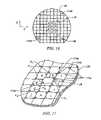
- FIG. 16is a top down view of a wafer, shown in FIGS. 2 , 5 and 6 upon which imprinting layers are disposed;
- FIG. 17is a detailed view of FIG. 16 showing the position of the mold in one of the imprint regions
- FIG. 18is a bottom-up plan view of the chuck body shown in FIG. 8 in accordance with an alternate embodiment
- FIG. 19is a cross-sectional view of a chuck body shown in FIG. 8 in accordance with a second alternate embodiment
- FIG. 20is a flow diagram showing a method of reducing distortions in patterns formed using imprint lithography techniques in accordance with the present invention.
- FIG. 21is a flow diagram showing a method of reducing distortions in patterns formed using imprint lithography techniques in accordance with an alternate embodiment of the present invention.
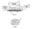
- FIG. 1depicts a lithographic system 10 in accordance with one embodiment of the present invention that includes a pair of spaced-apart bridge supports 12 having a bridge 14 and a stage support 16 extending therebetween. Bridge 14 and stage support 16 are spaced-apart. Coupled to bridge 14 is an imprint head 18 , which extends from bridge 14 toward stage support 16 . Disposed upon stage support 16 to face imprint head 18 is a motion stage 20 . Motion stage 20 is configured to move with respect to stage support 16 along X and Y axes.
- An exemplary motion stage deviceis disclosed in U.S.
- a radiation source 22is coupled to system 10 to impinge actinic radiation upon motion stage 20 .
- radiation source 22is coupled to bridge 14 and includes a power generator 23 connected to radiation source 22 .
- Mold 28includes a plurality of features defined by a plurality of spaced-apart recessions 28 a and protrusions 28 b .
- the plurality of featuresdefines an original pattern that is to be transferred into a wafer 30 positioned on motion stage 20 .
- imprint head 18is adapted to move along the Z axis and vary a distance “d” between mold 28 and wafer 30 .
- the features on mold 28may be imprinted into a flowable region of wafer 30 , discussed more fully below.
- Radiation source 22is located so that mold 28 is positioned between radiation source 22 and wafer 30 .
- mold 28is fabricated from material that allows it to be substantially transparent to the radiation produced by radiation source 22 .
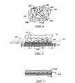
- a flowable regionsuch as an imprinting layer 34 , is disposed on a portion of surface 32 that presents a substantially planar profile.
- Flowable regionmay be formed using any known technique such as a hot embossing process disclosed in U.S. Pat. No. 5,772,905, which is incorporated by reference in its entirety herein, or a laser assisted direct imprinting (LADI) process of the type described by Chou et al. in Ultrafast and Direct Imprint of Nanostructures in Silicon , Nature, Col. 417, pp. 835–837, June 2002.
- LADIlaser assisted direct imprinting
- flowable regionconsists of imprinting layer 34 being deposited as a plurality of spaced-apart discrete beads 36 of material 36 a on wafer 30 , discussed more fully below.
- An exemplary system for depositing beads 36is disclosed in U.S. patent application Ser. No. 10/191,749, filed Jul. 9, 2002, entitled “System and Method for Dispensing Liquids”, and which is assigned to the assignee of the present invention.
- Imprinting layer 34is formed from a material 36 a that may be selectively polymerized and cross-linked to record the original pattern therein, defining a recorded pattern.
- An exemplary composition for material 36 ais disclosed in U.S. patent application Ser. No. 10/463,396, filed Jun.
- Material 36 ais shown in FIG. 4 as being cross-linked at points 36 b , forming cross-linked polymer material 36 c.
- the pattern recorded in imprinting layer 34is produced, in part, by mechanical contact with mold 28 .
- imprint head 18reduces the distance “d” to allow imprinting layer 34 to come into mechanical contact with mold 28 , spreading beads 36 so as to form imprinting layer 34 with a contiguous formation of material 36 a over surface 32 .
- distance “d”is reduced to allow sub-portions 34 a of imprinting layer 34 to ingress into and fill recessions 28 a.
- material 36 ais provided with the requisite properties to completely fill recessions 28 a while covering surface 32 with a contiguous formation of material 36 a .
- sub-portions 34 b of imprinting layer 34 in superimposition with protrusions 28 bremain after the desired, usually minimum distance “d”, has been reached, leaving sub-portions 34 a with a thickness t 1 , and sub-portions 34 b with a thickness, t 2 .
- Thicknesses “t 1 ” and “t 2 ”may be any thickness desired, dependent upon the application.
- t 1is selected so as to be no greater than twice the width u of sub-portions 34 a , i.e., t 1 ⁇ 2u, shown more clearly in FIG. 5 .
- radiation source 22produces actinic radiation that polymerizes and cross-links material 36 a , forming cross-linked polymer material 36 c .
- the composition of imprinting layer 34transforms from material 36 a to material 36 c , which is a solid.
- material 36 cis solidified to provide side 34 c of imprinting layer 34 with a shape conforming to a shape of a surface 28 c of mold 28 , shown more clearly in FIG. 5 .
- imprint head 18shown in FIG. 2 , is moved to increase distance “d” so that mold 28 and imprinting layer 34 are spaced-apart.
- additional processingmay be employed to complete the patterning of wafer 30 .
- wafer 30 and imprinting layer 34may be etched to transfer the pattern of imprinting layer 34 into wafer 30 , providing a patterned surface 32 a , shown in FIG. 6 .
- the material from which imprinting layer 34 is formedmay be varied to define a relative etch rate with respect to wafer 30 , as desired.
- the relative etch rate of imprinting layer 34 to wafer 30may be in a range of about 1.5:1 to about 100:1.
- imprinting layer 34may be provided with an etch differential with respect to photo-resist material (not shown) selectively disposed thereon.
- the photo-resist material (not shown)may be provided to further pattern imprinting layer 34 , using known techniques. Any etch process may be employed, dependent upon the etch rate desired and the underlying constituents that form wafer 30 and imprinting layer 34 . Exemplary etch processes may include plasma etching, reactive ion etching, chemical wet etching and the like.
- an exemplary radiation source 22may produce ultraviolet radiation.
- Other radiation sourcesmay be employed, such as thermal, electromagnetic and the like.
- the selection of radiation employed to initiate the polymerization of the material in imprinting layer 34is known to one skilled in the art and typically depends on the specific application which is desired.
- the plurality of features on mold 28are shown as recessions 28 a extending along a direction parallel to protrusions 28 b that provide a cross-section of mold 28 with a shape of a battlement.
- recessions 28 a and protrusions 28 bmay correspond to virtually any feature required to create an integrated circuit and may be as small as a few tenths of nanometers.
- bridge supports 12 , bridge 14 , and/or stage support 16may be fabricated from one or more of the following materials: silicon carbide, iron alloys available under the trade name INVAR®, or name SUPER INVARTM, ceramics, including but not limited to ZERODUR® ceramic.
- table 24may be constructed to isolate the remaining components of system 10 from vibrations in the surrounding environment. An exemplary table 24 is available from Newport Corporation of Irvine, Calif.
- template 26upon which mold 28 is present, is coupled to imprint head housing 18 a via a chucking system 40 that includes chuck body 42 .
- a calibration system 18 bis coupled to imprint head housing 18 a
- chuck body 42couples template 26 to calibration system 18 b vis-à-vis a flexure system 18 c .
- Calibration system 18 bfacilitates proper orientation alignment between template 26 and wafer 30 , shown in FIG. 5 , thereby achieving a substantially uniform gap distance, “d”, therebetween.
- calibration system 18 bincludes a plurality of actuators 19 a , 19 b and 19 c and a base plate 19 d .
- actuators 19 a , 19 b and 19 care connected between housing 18 a and base plate 19 d .
- Flexure system 18 cincludes flexure springs 21 a and flexure ring 21 b .
- Flexure ring 21 bis coupled between base plate 19 d and flexure springs 21 a .
- Motion of actuators 19 a , 19 b and 19 corientates flexure ring 21 b that may allow for a coarse calibration of flexure springs 21 a and, therefore, chuck body 42 and template 26 .
- Actuators 19 a , 19 b and 19 calso facilitate translation of flexure ring 21 b to the Z-axis.
- Flexure springs 21 ainclude a plurality of linear springs that facilitate gimbal-like motion in the X-Y plane so that proper orientation alignment may be achieved between wafer 30 and template 26 , shown in FIG. 2 .
- chuck body 42is adapted to retain template 26 upon which mold 28 is attached employing vacuum techniques.
- chuck body 42includes first 46 and second 48 opposed sides.
- a side, or edge, surface 50extends between first side 46 and second side 48 .
- First side 46includes a first recess 52 and a second recess 54 , spaced-apart from first recess 52 , defining first 58 and second 60 spaced-apart support regions.
- First support region 58cinctures second support region 60 and the first 52 and second 54 recesses.
- Second support region 60cinctures second recess 54 .
- a portion 62 of chuck body 42 in superimposition with second recess 54is transparent to radiation having a predetermined wavelength, such as the wavelength of the actinic radiation mentioned above.
- portion 62is made from a thin layer of transparent material, such as glass. However, the material from which portion 62 is made may depend upon the wavelength of radiation produced by radiation source 22 , shown in FIG. 2 .
- Portion 62extends from second side 48 and terminates proximate to second recess 54 and should define an area at least as large as an area of mold 28 so that mold 28 is in superimposition therewith.
- Formed in chuck body 42are one or more throughways, shown as 64 and 66 .
- One of the throughways, such as throughway 64places first recess 52 in fluid communication with side surface 50 .
- the remaining throughway, such as throughway 66places second recess 54 in fluid communication with side surface 50 .
- throughway 64may extend between second side 48 and first recess 52 , as well.
- throughway 66may extend between second side 48 and second recess 54 . What is desired is that throughways 64 and 66 facilitate placing recesses 52 and 54 , respectively, in fluid communication with a pressure control system, such a pump system 70 .
- Pump system 70may include one or more pumps to control the pressure proximate to recesses 52 and 54 , independently of one another. Specifically, when mounted to chuck body 42 , template 26 rests against first 58 and second 60 support regions, covering first 52 and second 54 recesses. First recess 52 and a portion 44 a of template 26 in superimposition therewith define a first chamber 52 a . Second recess 54 and a portion 44 b of template 26 in superimposition therewith define a second chamber 54 a . Pump system 70 operates to control a pressure in first 52 a and second 54 a chambers.
- the pressureis established in first chamber 52 a to maintain the position of the template 26 with the chuck body 42 and reduce, if not avoid, separation of template 26 from chuck body 42 under force of gravity.
- the pressure in the second chamber 54 amay differ from the pressure in the first chamber 52 a to, inter alia, reduce distortions in the template 26 that occur during imprinting, by modulating a shape of template 26 .
- pump system 70may apply a positive pressure in chamber 54 a to compensate for any upward force R that occurs as a result on imprinting layer 34 contacting mold 28 .
- pump system 70may apply a positive pressure in chamber 54 a to compensate for any upward force R that occurs as a result on imprinting layer 34 contacting mold 28 .
- the actuator device 72includes first and second bodies 74 and 76 , mounted on opposite sides of chuck body 42 , all of which are mounted to a flexure system 18 c .
- At least one of bodies body 74 and 76includes one or more chambers, shown in body 74 as 74 a .
- Disposed within chamber 74 ais an actuator arm.
- a first member 74 c of actuator arm 74 bis connected to body 74 to reciprocate about an axis 74 d .
- First member 74 cextends from axis 74 d along the Z direction and terminates in a second member 74 e .
- Second member 74 eextends from first member 74 c along the X direction and terminates in a contact member 74 f .
- At least one bladderis disposed within chamber 74 a .
- two bladders 78 a and 78 bare disposed in chamber on opposite sides of first member 74 c .
- bladder 78 bdisposed between a first sidewall 74 g of body 74 and first member 74 c
- bladder 78 bis disposed between a second side wall 74 h of body and first member 74 c .
- Each of bladders 78 a and 78 bhas a volume that may be selectively varied in response to introduction of a fluid therein. To that end, each bladder 78 a and 78 b is in fluid communication with pump system 70 .
- contact member 76 fDisposed opposite to contact member 74 f is contact member 76 f and spaced-apart a distance D 1 . It is not necessary for contact member 76 f to be coupled to move with respect to body 76 . As a result, contact member 76 f may be rigidly attached to body 76 . As shown, however, contact member is shown connected to a second portion of actuator arm 76 , and first member 76 c of actuator arm 76 b is connected to body 76 to reciprocate about an axis 76 d . First member 76 c extends from axis 76 d along the Z direction and terminates in a second member 76 e .
- Second member 76 eextends from first member 76 c along the X direction and terminates in a contact member 76 f .
- At least one bladderis disposed within chamber 76 a .
- two bladders 80 a and 80 bare disposed in chamber 76 a on opposite sides of first member 76 c .
- bladder 80 bdisposed between a first sidewall 76 g of body 76 and first member 76 c
- bladder 80 bis disposed between a second side wall 76 h of body and first member 76 c .
- Each of bladders 80 a and 80 bhas a volume that may be selectively varied in response to introduction of a fluid therein. To that end, each bladder 80 a and 80 b is in fluid communication with pump system 70 .
- template 26is disposed between contact members.
- the distance D 1is established to be slightly smaller than the distance between the opposed regions of perimeter surface 26 a of template 26 in contacted therewith.
- template 26is described as being compressively pre-loaded.
- one or both of bladders 78 a and 80 amay be inflated to increase the volume thereof. Expansion of bladder 78 a causes actuator arm 74 b to move about axis 74 d toward sidewall 74 h , thereby decreasing the magnitude of distance D 1 . Expansion of bladder 80 a causes actuator arm 76 b to move about axis 76 d toward sidewall 76 h , thereby decreasing the magnitude of distance D 1 .
- the volume of bladders 78 a and 80 amay be reduced to return to nominal size.
- one or both of bladders 78 b and 80 bmay be expanded. Expansion of bladder 78 b causes actuator arm 74 b to move about axis 74 d toward sidewall 74 g , thereby increasing the magnitude of distance D 1 . Expansion of bladder 80 b causes actuator arm 76 b to move about axis 76 d toward sidewall 76 g , thereby increasing the magnitude of distance D 1 .
- Expansion of bladders 78 b and 80 bmay also occur as the volume of bladders 78 a and 80 a is decreased.
- a rate at which one or more of bladders 78 b and 80 b are expanded and one or both of bladders 78 b and 80 b are deflatedthe time required to return substrate to a compressively pre-loaded state may be reduced
- a problem encountered during operationconcerned a force applied against side walls 74 g and 76 g when large compression forces were applied to perimeter surface 26 a .
- expansion of bladder 78 aexerted a force applied to side wall 76 g
- expansion of bladder 80 aexerted a force on side wall 76 g .
- the forces exerted on one or both of side walls 74 g and 76 gresulted in bending moment on chuck body 42 , which is transmitted onto template 26 .
- template 26should be subjected to purely compressive forces, with bending forces being substantially minimized, if not avoid entirely. Bending forces on substrate are problematic in that is results in pattern distortion.
- a compression ring 79is provided.
- Compression ring 79surrounds an area 81 and includes a surface 79 a facing the area 81 .
- Bodies 74 and 76are connected to surface 79 a and disposed opposite one another.
- the force exerted by bladder 78 a on sidewall 74 gcreates an equal and opposite force on a region of compression ring 79 disposed opposite to body 74 .
- the force exerted by bladder 80 a on sidewall 76 gcreates an equal and opposite force on a region of compression ring 79 disposed opposite to body 76 .
- a neutral axis 79 a thereofis closely aligned with a neutral axis A of template 26 .
- actuator device 72it is possible to employ actuator device 72 to expand template 26 , as well.
- contact members 74 f and 76 fwould be fixedly attached to perimeter surface 26 a . This may be achieved, for example, with the use of adhesives.
- the second members 74 e and 76 ewould then be coupled to contact members, 74 f and 76 f , respectively by, for example, a threaded coupling and/or adhesives.
- Tensile forceswould be applied to template 26 by expanding one or both of bladders 78 b and 80 b.
- An advantage with the present designis that the entire actuator device 72 is positioned to lie on one side of mold 28 so as to be spaced-apart from a plane in which mold surface 28 c lies. This is beneficial in preventing contact between the components of actuator device 72 and a wafer 30 , shown in FIG. 5 , during imprint processes. Additionally, by providing a relatively long firm member 74 c and 76 c , that area upon which a force may be exerted by bladders 74 a , 74 b , 76 a and 76 b may be substantially increased. This facilitates increasing the per unit area of force applied to perimeter surface 76 a by contact members 74 f and 76 f .
- the amplification of the force per unit area exerted by contact member 74 fis a function of the ratio of two areas: the area of perimeter surface 26 a upon which contact members 74 f exerts a force and the area of first member 74 fc over which one of bladders 78 a and 78 b exerts a force.
- the amplification of the force per unit area exerted by contact member 76 fis a function of the ratio of two areas: the area of perimeter surface 26 a upon which contact members 76 f exerts a force and the area of first member 76 c over which one of bladders 80 a and 80 b exerts a force.
- Bladders 78 a , 78 b , 80 a , and 80 bprovide an additional advantage of avoiding localized force concentration on actuator arms 74 b and 76 b due to, for example, roughness of the surface in contact therewith. Specifically, the surface roughness of actuator arms 74 b and 76 b may result in an uneven distribution of the force applied thereon by bladders 78 a , 78 b , 80 a , and 80 b . As a result, there can be localized surface concentrations of the force created by the bladders 78 a , 78 b , 80 a , and 80 b that may result in non-linear compression.
- Bladders 78 a , 78 b , 80 a , and 80 breduce, if not avoid, this problem by being formed of compliant material that takes the shape of the area against which contact is made. As a result, an even distribution of forces is exerted on over the contact area. For similar reasons, it may be desired to form contact members 74 f and 76 f from compliant material so that the same forms a profile that matches the profile of the perimeter surface 26 a that comes in contact therewith.
- compliant bladders 78 a , 78 b , 80 a , and 80 bcompensates for any non-planarity and/or roughness over the area of perimeter surface 26 a , referred hereafter as surface anomalies, that comes into contact with the contact members 74 f and 76 f .
- bladders 78 a , 78 b , 80 a , and 80 bmay conform to any distortion of first members 74 c and 76 c result from any bending moment exerted thereupon by contact members 74 f and 76 f .
- body 74may include a plurality of contact members, shown as 174 f , 274 f , 374 f and 474 f , each of which is attached to a separate actuator arm (not shown) that is mounted to body 74 as discussed above with respect to actuator arm 74 b .
- Bladders 78 a and 78 bcould facilitate movement of contact members as discussed above with respect to contact member 74 f .
- body 76may include a plurality of include a plurality of contact members, shown as 176 f , 276 f , 376 f and 476 f , each of which is attached to a separate actuator arm (not shown) that is mounted to body 76 , as discussed above with respect to actuator arm 76 b .
- Bladders 80 a and 80 bcould facilitate movement of contact members 176 f , 276 f , 376 f and 476 f with respect to contact member 76 f.
- bladder 78 amay be replaced with a plurality of bladders 178 a , 278 a , 378 a , 478 a , each of which is in fluid communication with pump system 70 .
- Each of the plurality of bladders 178 a , 278 a , 378 a , 478 ais coupled to move one of contact members 174 f , 274 f , 374 f , 474 f that differs from the contact members 174 f , 274 f , 374 f , 474 f that the remaining bladders 178 a , 278 a , 378 a , 478 a are coupled to move.
- bladder 80 amay be replaced with a plurality of bladders 180 a , 280 a , 380 a , 480 a , each of which is in fluid communication with pump system 70 .
- Each of bladders 180 a , 280 a , 380 a , 480 ais coupled to move one of contact members 176 f , 276 f , 376 f , 476 f that differs from the contact members 176 f , 276 f , 376 f , 476 f that the remaining bladders 180 a , 280 a , 380 a , 480 a are coupled to move.
- bladders 78 b and 80 bmay also be replaced with a plurality of bladders to achieve independent control over contact members 174 a , 274 f , 374 f , 474 f , 176 f , 276 f , 376 f and 476 f when applying a tensile force to template 26 .
- An additional benefit with providing independent control over the movement of the plurality of contact members 174 f , 274 f , 374 f , 474 f , 176 f , 276 f , 376 f and 476 fis that is facilitates compensation for errors caused by anisotropic thermal expansion of template 26 .
- bladders 78 a , 78 b , 80 a , 80 b , 178 a , 278 a , 378 a , 478 a , 180 a . 280 a , 380 a and 480 awith a piezo actuator, four of which are shown as 500 , 502 , 504 and 506 .
- each of piezo actuatorsis coupled to body 76 via flexures 500 b , 502 b , 504 b and 506 b , respectively.
- piezo actuators 500 , 502 , 504 and 506may be employed to compensate for surface anomalies and bladders 178 a , 278 a , 378 a and 478 a may be employed to compensate for large mean errors for differing templates coupled to chuck body 42 . This facilitates maintaining template 26 centering respect to a machine coordinate frame.
- piezo actuatorsare shown in combination with the plurality of bladders 178 a , 278 a , 378 a and 478 a
- any combination piezo actuators and bladdersmay be employed in actuator device 72 .
- only one piezo actuatormay be employed on one body for example, body, 74 , with body 76 contact one or more contact members being rigidly attached thereto or having including any of the bladder combinations shown in FIGS. 11 , 12 and 13 .
- all bladders associated with compression devicebe replaced with piezo actuators.
- the dimension of template 26may be varied in two dimensions. This is particularly useful in overcoming Poisson's effect. Poisson's effect may result in linear coupling of template 26 that may necessitate activating actuators to vary both distances D 1 and D 2 .
- the Poisson ratiois the ratio between the tensile strain caused in the Y and Z directions in template 26 to the compressive strain imparted to template 26 in the X direction. Typical numbers are in the range of 0.1–0.4.
- Were template 26 formed from fused silicais the ratio is approximately 0.16.
- actuator device 72a force may be applied to template 26 to vary the dimensions of the same and reduce distortions in the pattern recorded into imprinting layer 34 , shown in FIG. 2 .
- distortions in the pattern recorded into imprinting layer 34may arise from, inter alia, dimensional variations of imprinting layer 34 and wafer 30 . These dimensional variations, which may be due in part to thermal fluctuations, as well as, inaccuracies in previous processing steps that produce what is commonly referred to as magnification/run-out errors.
- the magnification/run-out errorsoccur when a region of wafer 30 in which the original pattern is to be recorded exceeds the area of the original pattern. Additionally, magnification/run-out errors may occur when the region of wafer 30 , in which the original pattern is to be recorded, has an area smaller than the original pattern.
- imprinting layer 124in superimposition with patterned surface 32 a , shown in FIG. 6 .
- Proper alignment between two superimposed patternsis difficult in the face of magnification/run-out errors in both single-step full wafer imprinting and step-and-repeat imprinting processes.
- a step-and-repeat processincludes defining a plurality of regions, shown as, a– 1 , on wafer 30 in which the original pattern on mold 28 will be recorded.
- the original pattern on mold 28may be coextensive with the entire surface of mold 28 , or simply located to a sub-portion thereof. The present invention will be discussed with respect to the original pattern being coextensive with the surface of mold 28 that faces wafer 30 .
- Proper execution of a step-and-repeat processmay include proper alignment of mold 28 with each of regions a– 1 . To that end, mold 28 includes alignment marks 114 a , shown as a “+” sign.
- One or more of regions a– 1includes fiducial marks 110 a .
- fiducial marks 110 aBy ensuring that alignment marks 114 a are properly aligned with fiducial marks 110 a , proper alignment of mold 28 with one of regions a– 1 in superimposition therewith is ensured.
- machine vision devices(not shown) may be employed to sense the relative alignment between alignment marks 114 a and fiducial marks 110 a . In the present example, proper alignment is indicated upon alignment marks 114 a being in superimposition with fiducial marks 110 a . With the introduction of magnification/run-out errors, proper alignment becomes very difficult.
- magnification/run-out errorsare reduced, if not avoided, by creating relative dimensional variations between mold 28 and wafer 30 .
- the temperature of wafer 30is varied so that one of regions a– 1 defines an area that is slightly less than an area of the original pattern on mold 28 .
- the final compensation for magnification/run-out errorsis achieved by subjecting template 26 , shown in FIG. 8 , to mechanical compression forces using actuator device 72 , which are in turn transferred to mold 28 shown by arrows F 1 and F 2 , orientated transversely to one another, shown in FIG. 17 .
- the area of the original patternis made coextensive with the area of the region a– 1 in superimposition therewith.
- subjecting template 26 to compressive forcesmodulates the shape of the same through bending action. Bending of template 26 may also introduce distortions in the pattern imprinted into imprinting layer 34 . The pattern distortions attributable to bending of template 26 may be reduced, if not prevented, by positioning actuator device 72 so that the bending of template 26 is controlled to occur in a desired direction. In the present example, actuator device 72 is positioned to compress template 26 so as to bow in a direction parallel to, and opposite of, force R.
- chucking system 40may be employed to counter the bending force, B, so as to establish mold 28 to be a desired shape, e.g., arcuate, planar and the like.
- Pump system 70may be employed to pressurize chamber 54 a appropriately to that end. For example, assuming bending force, B, is greater than force R, pump system 70 would be employed to evacuate chamber 54 a with sufficient vacuum to counter the bending force B. Were bending force B weaker than force, R, pump system 70 would be employed to pressurize chamber 54 a appropriately to maintain planarity of mold 28 , or any other desired shape.
- the exact pressure levelsmay be determined with a priori knowledge of the forces R and B which then may be analyzed by a processor (not shown) that may be included in pump system 70 to pressurize chambers 52 a and 54 a to the appropriate levels. Also, the forces R and B may be sensed dynamically using known techniques so that the pressure within chambers 52 a and 54 a may be established dynamically during operation to maintain template 26 with a desired shape. An added benefit is that the pressure in one or both chambers 52 a and 54 a may be established to be a positive pressure, thereby facilitating removal of template 26 from chuck body 42 . This also may be accomplished under processor control, or manually.
- support regions 58 and 60have surface regions 58 a and 60 a , respectively, formed thereon from a material adapted to conform to a profile of said template 26 and resistant to deformation along the X and Y axes. In this manner, surface regions 58 a and 60 a resist relative movement of template 26 with respect to chuck body 42 in the X and Y directions.
- chuck body 142may include one or more walls, or baffles, shown as 142 a , 142 b , 142 c and 142 d extending between first and second support regions 158 and 160 .
- walls/baffles 142 a , 142 b , 142 c and 142 dsegment recess 152 into a plurality of sub-regions 152 a , 152 b , 152 c and 152 d that function as sub-chambers once template 26 is placed in superimposition therewith.
- Sub-chambers 152 a , 152 b , 152 c and 152 dmay be fluid-tight which would result in each have a throughway (not shown) placing the same in fluid communication with pump system 70 .
- sub-chambers 152 a , 152 b , 152 c and 152 dmay not form fluid-tight chambers once template 26 is placed in superimposition therewith. Rather walls 142 a , 142 b , 142 c and 142 d would be spaced apart from template 26 to function as a baffle for fluid transfer across the same.
- a pressure differentialcould be provided between sub-chambers 152 a , 152 b , 152 c and 152 d , as desired.
- sub-regions 152 a , 152 b , 152 c and 152 dmay be concurrently provided with differing pressure levels.
- the amount of force exerted on template 26 when being pulled-apart from imprinting layer 34may vary across the surface of template 26 . This allows cantilevering, or peeling-off of template 26 from imprinting layer 34 that reduces distortions or defects from being formed in imprinting layer 34 during separation of template 26 therefrom.
- sub-chamber 152 bmay have a pressure established therein that is greater than the pressure associated with the remaining sub-chambers 152 a , 152 c and 152 d .
- the pulling force of the portion of template 26 in superimposition with sub-chambers 152 a , 152 c and 152 d is subjected tois greater than the pulling force to which the portion of template 26 in superimposition with sub-chamber 152 b is subjected.
- the rate that “d” increases for the portion of template 26 in superimposition with sub-chambers 152 a , 152 c and 152 dis accelerated compared to the rate at which “d” increases for the portion of template 26 in superimposition with sub-chamber 152 b , providing the aforementioned cantilevering effect.
- chuck body 242includes a plurality of pins 242 a projecting from a nadir surface 252 a of out recess 252 .
- Pins 242 aprovide mechanical support for the wafer (not shown] retained on chuck body 242 via vacuum. This enables support regions 258 and 260 to have surface regions 258 a and 260 a , respectively, formed from material that is fully compliant with the surface (not shown) of the wafer (not shown) resting against support regions 258 and 260 .
- surface regions 258 a and 260 aprovide a fluid-tight seal with the wafer (not shown) in the presence of extreme surface variation, e.g., when particulate matter is present between the surface (not shown) of the wafer (not shown) and the surface regions 258 a and 260 a .
- Mechanical support of the wafer (not shown) in the Z directionneed not be provided by surface regions 258 a and 260 a .
- Pins 242 aprovide this support. To that end, pins 242 a are typically rigid posts having a circular cross-section.
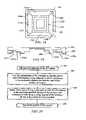
- an accurate measurement of wafer 30 in an X-Y planeis undertaken at step 200 .
- Thismay be achieved by sensing gross alignment fiducials 110 b present on wafer 30 using machine vision devices (not shown) and known signal processing techniques.
- the temperature of wafer 30may be varied, i.e., raised or lowered, so that the area of one of regions a– 1 is slightly less than an area of the original pattern on mold 28 .
- the temperature variationsmay be achieved using a temperature controlled chuck or pedestal (not shown) against which wafer 30 rests.
- the area of each of regions a– 1can be determined by measurement of a change in distance between two collinear gross alignment fiducials 110 b.
- a change in the distance between two gross alignment fiducials 110 b collinear along one of the X or Y axesis determined. Thereafter, this change in distance is divided by a number of adjacent regions a– 1 on the wafer 30 along the X-axis. This provides the dimensional change of the areas of regions a– 1 attributable to dimensional changes in wafer 30 along the X-axis. If necessary the same measurement may be made to determine the change in area of regions a– 1 due to dimensional changes of wafer 30 along the Y-axis. However, it may also be assumed that the dimensional changes in wafer 30 may be uniform in the two orthogonal axes, X and Y.
- compressive forces, F 1 and F 2are applied to mold 28 to establish the area of the original pattern to be coextensive with the area of one of the regions a– 1 in superimposition with the pattern. This may be achieved in real-time employing machine vision devices (not shown) and known signal processing techniques, to determine when two or more of alignment marks 114 a are aligned with two or more of fiducial marks 110 a .
- the original patternis recorded in the region a– 1 that is in superimposition with mold 28 , forming the recorded pattern.
- compression forces F 1 and F 2have the same magnitude, as the dimensional variations in either wafer 30 or mold 28 may not be uniform in all directions. Further, the magnification/run-out errors may not be identical in both X-Y directions. As a result, compression forces, F 1 and F 2 may differ to compensate for these anomalies. Furthermore, to ensure greater reduction in magnification/run-out errors, the dimensional variation in mold 28 may be undertaken after mold 28 contacts imprinting layer 124 , shown in FIG. 6 . However, this is not necessary.
- the alignment of mold 28 with regions a– 1 in superimposition therewithmay occur with mold 28 being spaced-apart from imprinting layer 124 .
- the magnification/run-out errorswere constant over the entire wafer 30 , then the magnitude of forces F 1 and F 2 could be maintained for each region a– 1 in which the original pattern is recorded.
- steps 202 and 204shown in FIG. 15 , would then be undertaken for each region a– 1 in which the original pattern is recorded.
- the area of the regions a– 1should be of appropriate dimensions to enable pattern on mold 28 to define an area coextensive therewith when mold 28 is subject to compression forces F 1 and F 2 , without compromising the structural integrity of mold 28 .
- step 300accurate measurement of wafer 30 in an X-Y plane is undertaken at step 300 .
- step 302the dimensions of one of regions a– 1 in superimposition with mold 28 is determined.
- step 304it is determined whether the area of one of regions a– 1 in superimposition with mold 28 is larger than the area of the pattern on mold 28 . If this is the case, the process proceeds to step 306 , otherwise the process proceeds to step 308 .
- step 308mold 28 is placed in contact with the region a– 1 in superimposition therewith, and the requisite magnitude of compressive forces F 1 and F 2 is determined to apply to mold 28 to ensure that the area of pattern is coextensive with the area of this region a– 1 .
- step 310compressive forces F 1 and F 2 are applied to mold 28 .
- mold 28is spaced-apart from the region a– 1 in superimposition with mold 28 and the process proceeds to step 312 where it is determined whether there remain any regions a– 1 on wafer 30 in which to record the original pattern. If there are, the process proceeds to step 314 wherein mold is placed in superimposition with the next region and the process proceeds to step 304 . Otherwise, the process ends at step 316 .
- step 304Were it determined at step 304 that the region a– 1 in superimposition with mold 28 had an area greater than the area of the pattern, then the process proceeds to step 306 wherein the temperature of mold 28 is varied to cause expansion of the same.
- mold 28is heated at step 306 so that the pattern is slightly larger than the area of region a– 1 in superimposition therewith. Then the process continues at step 310 .
- LADIlaser assisted direct imprinting
Landscapes
- Engineering & Computer Science (AREA)
- Nanotechnology (AREA)
- Chemical & Material Sciences (AREA)
- Physics & Mathematics (AREA)
- General Physics & Mathematics (AREA)
- Crystallography & Structural Chemistry (AREA)
- Manufacturing & Machinery (AREA)
- Condensed Matter Physics & Semiconductors (AREA)
- Mathematical Physics (AREA)
- Theoretical Computer Science (AREA)
- Mechanical Engineering (AREA)
- Microelectronics & Electronic Packaging (AREA)
- Shaping Of Tube Ends By Bending Or Straightening (AREA)
Abstract
Description
Claims (22)
Priority Applications (8)
| Application Number | Priority Date | Filing Date | Title |
|---|---|---|---|
| US10/616,294US7150622B2 (en) | 2003-07-09 | 2003-07-09 | Systems for magnification and distortion correction for imprint lithography processes |
| CNA2004800230671ACN1871103A (en) | 2003-07-09 | 2004-07-08 | Systems for magnification and distortion correction for imprint lithography processes |
| JP2006518977AJP4594305B2 (en) | 2003-07-09 | 2004-07-08 | System for correcting magnification and distortion in imprint lithography processes |
| PCT/US2004/022454WO2005006076A2 (en) | 2003-07-09 | 2004-07-08 | Systems for magnification and distortion correction for imprint lithography processes |
| TW093120450ATW200522155A (en) | 2003-07-09 | 2004-07-08 | Systems for magnification and distortion correction for imprint lithography processes |
| KR1020067000555AKR20060034694A (en) | 2003-07-09 | 2004-07-08 | Zoom and distortion correction system for imprint lithography process |
| EP04778126AEP1642170A4 (en) | 2003-07-09 | 2004-07-08 | Systems for magnification and distortion correction for imprint lithography processes |
| MYPI20042743AMY137556A (en) | 2003-07-09 | 2004-07-09 | Systems for magnification and distortion correction for imprint lithography processes |
Applications Claiming Priority (1)
| Application Number | Priority Date | Filing Date | Title |
|---|---|---|---|
| US10/616,294US7150622B2 (en) | 2003-07-09 | 2003-07-09 | Systems for magnification and distortion correction for imprint lithography processes |
Publications (2)
| Publication Number | Publication Date |
|---|---|
| US20050006343A1 US20050006343A1 (en) | 2005-01-13 |
| US7150622B2true US7150622B2 (en) | 2006-12-19 |
Family
ID=33564732
Family Applications (1)
| Application Number | Title | Priority Date | Filing Date |
|---|---|---|---|
| US10/616,294Expired - LifetimeUS7150622B2 (en) | 2003-07-09 | 2003-07-09 | Systems for magnification and distortion correction for imprint lithography processes |
Country Status (8)
| Country | Link |
|---|---|
| US (1) | US7150622B2 (en) |
| EP (1) | EP1642170A4 (en) |
| JP (1) | JP4594305B2 (en) |
| KR (1) | KR20060034694A (en) |
| CN (1) | CN1871103A (en) |
| MY (1) | MY137556A (en) |
| TW (1) | TW200522155A (en) |
| WO (1) | WO2005006076A2 (en) |
Cited By (29)
| Publication number | Priority date | Publication date | Assignee | Title |
|---|---|---|---|---|
| US20050208171A1 (en)* | 2004-02-20 | 2005-09-22 | Canon Kabushiki Kaisha | Mold and molding apparatus using the same |
| US20060231979A1 (en)* | 2005-04-19 | 2006-10-19 | Asml Netherlands B.V. | Imprint lithography |
| US20060233906A1 (en)* | 2005-04-19 | 2006-10-19 | Toshiba Kikai Kabushiki Kaisha | Transcript apparatus |
| US20060243761A1 (en)* | 2005-04-28 | 2006-11-02 | Toshiba Kikai Kabushiki Kaisha | Transfer apparatus having gimbal mechanism and transfer method using the transfer apparatus |
| US20060257514A1 (en)* | 2005-05-10 | 2006-11-16 | Toshiba Kikai Kabushiki Kaisha | Transcript apparatus |
| US20060269645A1 (en)* | 2005-05-25 | 2006-11-30 | Toshiba Kikai Kabushiki Kaisha | Transcript apparatus |
| US20070287081A1 (en)* | 2004-06-03 | 2007-12-13 | Molecular Imprints, Inc. | Method for obtaining force combinations for template deformation using nullspace and methods optimization techniques |
| US20080160129A1 (en)* | 2006-05-11 | 2008-07-03 | Molecular Imprints, Inc. | Template Having a Varying Thickness to Facilitate Expelling a Gas Positioned Between a Substrate and the Template |
| US20090026657A1 (en)* | 2007-07-20 | 2009-01-29 | Molecular Imprints, Inc. | Alignment System and Method for a Substrate in a Nano-Imprint Process |
| US20090140445A1 (en)* | 2007-12-04 | 2009-06-04 | Molecular Imprints | High Throughput Imprint Based on Contact Line Motion Tracking Control |
| US7635263B2 (en) | 2005-01-31 | 2009-12-22 | Molecular Imprints, Inc. | Chucking system comprising an array of fluid chambers |
| US7636999B2 (en) | 2005-01-31 | 2009-12-29 | Molecular Imprints, Inc. | Method of retaining a substrate to a wafer chuck |
| US7641840B2 (en) | 2002-11-13 | 2010-01-05 | Molecular Imprints, Inc. | Method for expelling gas positioned between a substrate and a mold |
| US20100007868A1 (en)* | 2004-05-28 | 2010-01-14 | Board Of Regents, The University Of Texas System | Substrate Support System Having a Plurality of Contact Lands |
| US7670530B2 (en) | 2006-01-20 | 2010-03-02 | Molecular Imprints, Inc. | Patterning substrates employing multiple chucks |
| US7670529B2 (en) | 2005-12-08 | 2010-03-02 | Molecular Imprints, Inc. | Method and system for double-sided patterning of substrates |
| US20100102469A1 (en)* | 2008-10-24 | 2010-04-29 | Molecular Imprints, Inc. | Strain and Kinetics Control During Separation Phase of Imprint Process |
| US20100110409A1 (en)* | 2008-10-30 | 2010-05-06 | Molecular Imprints, Inc. | Separation in an Imprint Lithography Process |
| US20100320645A1 (en)* | 2009-06-19 | 2010-12-23 | Molecular Imprints, Inc. | Dual zone template chuck |
| US20110042348A1 (en)* | 2005-10-18 | 2011-02-24 | Canon Kabushiki Kaisha | Imprint method, imprint apparatus, and process for producing chip |
| US20110084417A1 (en)* | 2009-10-08 | 2011-04-14 | Molecular Imprints, Inc. | Large area linear array nanoimprinting |
| US20120056350A1 (en)* | 2010-09-06 | 2012-03-08 | Canon Kabushiki Kaisha | Original and article manufacturing method using same |
| US8215946B2 (en) | 2006-05-18 | 2012-07-10 | Molecular Imprints, Inc. | Imprint lithography system and method |
| US8715515B2 (en) | 2009-03-23 | 2014-05-06 | Intevac, Inc. | Process for optimization of island to trench ratio in patterned media |
| US9329316B2 (en) | 2013-08-27 | 2016-05-03 | Samsung Electronics Co., Ltd. | Wire grid polarizer and liquid crystal display panel and liquid crystal display device having the same |
| US9335582B2 (en) | 2013-05-29 | 2016-05-10 | Samsung Electronics Co., Ltd. | Wire grid polarizer, and liquid crystal display panel and liquid crystal display device including the same |
| US9375872B2 (en) | 2011-11-28 | 2016-06-28 | Canon Kabushiki Kaisha | Imprint apparatus, manufacturing method for article using the same, and imprint method |
| US20160195823A1 (en)* | 2009-07-06 | 2016-07-07 | Asml Netherlands B.V. | Imprint lithography apparatus and method |
| US10606170B2 (en) | 2017-09-14 | 2020-03-31 | Canon Kabushiki Kaisha | Template for imprint lithography and methods of making and using the same |
Families Citing this family (33)
| Publication number | Priority date | Publication date | Assignee | Title |
|---|---|---|---|---|
| US20050064344A1 (en)* | 2003-09-18 | 2005-03-24 | University Of Texas System Board Of Regents | Imprint lithography templates having alignment marks |
| US7019819B2 (en)* | 2002-11-13 | 2006-03-28 | Molecular Imprints, Inc. | Chucking system for modulating shapes of substrates |
| US8349241B2 (en)* | 2002-10-04 | 2013-01-08 | Molecular Imprints, Inc. | Method to arrange features on a substrate to replicate features having minimal dimensional variability |
| US20050270516A1 (en)* | 2004-06-03 | 2005-12-08 | Molecular Imprints, Inc. | System for magnification and distortion correction during nano-scale manufacturing |
| US7785526B2 (en) | 2004-07-20 | 2010-08-31 | Molecular Imprints, Inc. | Imprint alignment method, system, and template |
| US7292326B2 (en)* | 2004-11-30 | 2007-11-06 | Molecular Imprints, Inc. | Interferometric analysis for the manufacture of nano-scale devices |
| US7630067B2 (en) | 2004-11-30 | 2009-12-08 | Molecular Imprints, Inc. | Interferometric analysis method for the manufacture of nano-scale devices |
| JP4773729B2 (en)* | 2005-02-28 | 2011-09-14 | キヤノン株式会社 | Transfer apparatus and device manufacturing method |
| US7803308B2 (en) | 2005-12-01 | 2010-09-28 | Molecular Imprints, Inc. | Technique for separating a mold from solidified imprinting material |
| US7906058B2 (en)* | 2005-12-01 | 2011-03-15 | Molecular Imprints, Inc. | Bifurcated contact printing technique |
| US7802978B2 (en)* | 2006-04-03 | 2010-09-28 | Molecular Imprints, Inc. | Imprinting of partial fields at the edge of the wafer |
| US7946837B2 (en)* | 2006-10-06 | 2011-05-24 | Asml Netherlands B.V. | Imprint lithography |
| US7632088B2 (en)* | 2006-10-20 | 2009-12-15 | Provost Fellows And Scholars Of The College Of The Holy And Undivided Trinity Of Queen Elizabeth Near Dublin | Cyclic loading system and methods for forming nanostructures |
| NL1036034A1 (en)* | 2007-10-11 | 2009-04-15 | Asml Netherlands Bv | Imprint lithography. |
| JP5065121B2 (en)* | 2008-03-28 | 2012-10-31 | 東京エレクトロン株式会社 | Resist solution supply apparatus, resist solution supply method, program, and computer storage medium |
| US8043085B2 (en)* | 2008-08-19 | 2011-10-25 | Asml Netherlands B.V. | Imprint lithography |
| NL2004266A (en) | 2009-04-27 | 2010-10-28 | Asml Netherlands Bv | An actuator. |
| NL2004409A (en) | 2009-05-19 | 2010-11-22 | Asml Netherlands Bv | Imprint lithography apparatus. |
| US8913230B2 (en)* | 2009-07-02 | 2014-12-16 | Canon Nanotechnologies, Inc. | Chucking system with recessed support feature |
| JP5669466B2 (en)* | 2010-07-12 | 2015-02-12 | キヤノン株式会社 | Holding apparatus, imprint apparatus and article manufacturing method |
| JP5337114B2 (en)* | 2010-07-30 | 2013-11-06 | 株式会社東芝 | Pattern formation method |
| JP4774125B2 (en)* | 2010-10-04 | 2011-09-14 | キヤノン株式会社 | Transfer apparatus, mold, and device manufacturing method |
| JP5744548B2 (en)* | 2011-02-02 | 2015-07-08 | キヤノン株式会社 | Holding device, imprint apparatus using the same, and article manufacturing method |
| JP6061524B2 (en)* | 2011-08-11 | 2017-01-18 | キヤノン株式会社 | Imprint apparatus and article manufacturing method |
| JP5759303B2 (en)* | 2011-08-11 | 2015-08-05 | キヤノン株式会社 | Imprint apparatus and article manufacturing method using the same |
| US11267012B2 (en)* | 2014-06-25 | 2022-03-08 | Universal Display Corporation | Spatial control of vapor condensation using convection |
| EP2960059B1 (en) | 2014-06-25 | 2018-10-24 | Universal Display Corporation | Systems and methods of modulating flow during vapor jet deposition of organic materials |
| US11220737B2 (en) | 2014-06-25 | 2022-01-11 | Universal Display Corporation | Systems and methods of modulating flow during vapor jet deposition of organic materials |
| JP6552329B2 (en)* | 2014-09-12 | 2019-07-31 | キヤノン株式会社 | Imprint apparatus, imprint system, and article manufacturing method |
| US10331027B2 (en)* | 2014-09-12 | 2019-06-25 | Canon Kabushiki Kaisha | Imprint apparatus, imprint system, and method of manufacturing article |
| JP6552185B2 (en)* | 2014-11-20 | 2019-07-31 | キヤノン株式会社 | Imprint apparatus, correction mechanism calibration method, and article manufacturing method |
| US10566534B2 (en) | 2015-10-12 | 2020-02-18 | Universal Display Corporation | Apparatus and method to deliver organic material via organic vapor-jet printing (OVJP) |
| US11454883B2 (en) | 2016-11-14 | 2022-09-27 | Canon Kabushiki Kaisha | Template replication |
Citations (110)
| Publication number | Priority date | Publication date | Assignee | Title |
|---|---|---|---|---|
| US3783520A (en) | 1970-09-28 | 1974-01-08 | Bell Telephone Labor Inc | High accuracy alignment procedure utilizing moire patterns |
| DE2800476A1 (en) | 1977-01-07 | 1978-07-13 | Instruments Sa | Mass prodn. method for grids, graticules etc. - using revolving drum, belt carrying resin and UV light source for polymerisation process |
| US4256829A (en) | 1977-05-11 | 1981-03-17 | U.S. Philips Corporation | Method of manufacturing solid-state devices in which planar dimensional distortion is reduced |
| US4326805A (en) | 1980-04-11 | 1982-04-27 | Bell Telephone Laboratories, Incorporated | Method and apparatus for aligning mask and wafer members |
| US4492554A (en)* | 1980-08-26 | 1985-01-08 | Corn States Metal Fabricators, Inc. | Valve unit for a mold vent |
| US4512848A (en) | 1984-02-06 | 1985-04-23 | Exxon Research And Engineering Co. | Procedure for fabrication of microstructures over large areas using physical replication |
| US4600309A (en) | 1982-12-30 | 1986-07-15 | Thomson-Csf | Process and apparatus for theoptical alignment of patterns in two close-up planes in an exposure means incorporating a divergent radiation source |
| US4724222A (en) | 1986-04-28 | 1988-02-09 | American Telephone And Telegraph Company, At&T Bell Laboratories | Wafer chuck comprising a curved reference surface |
| US4731155A (en) | 1987-04-15 | 1988-03-15 | General Electric Company | Process for forming a lithographic mask |
| US4848911A (en) | 1986-06-11 | 1989-07-18 | Kabushiki Kaisha Toshiba | Method for aligning first and second objects, relative to each other, and apparatus for practicing this method |
| JPH01196749A (en) | 1988-01-30 | 1989-08-08 | Hoya Corp | Manufacture of substrate for optical information recording medium |
| JPH0292603A (en) | 1988-09-30 | 1990-04-03 | Hoya Corp | Manufacture of data recording board with guide groove |
| US4929083A (en) | 1986-06-19 | 1990-05-29 | Xerox Corporation | Focus and overlay characterization and optimization for photolithographic exposure |
| JPH0224848B2 (en) | 1981-11-13 | 1990-05-30 | Nippon Synthetic Chem Ind | |
| US5028366A (en) | 1988-01-12 | 1991-07-02 | Air Products And Chemicals, Inc. | Water based mold release compositions for making molded polyurethane foam |
| US5066351A (en)* | 1987-05-20 | 1991-11-19 | The Boeing Company | Hot/cold press forming methods for shaping thermoformable materials |
| US5072126A (en) | 1990-10-31 | 1991-12-10 | International Business Machines Corporation | Promixity alignment using polarized illumination and double conjugate projection lens |
| US5074667A (en) | 1988-08-15 | 1991-12-24 | Sumitomo Heavy Industries Co. Ltd. | Position detector employing a sector fresnel zone plate |
| US5148037A (en) | 1988-09-09 | 1992-09-15 | Canon Kabushiki Kaisha | Position detecting method and apparatus |
| US5148036A (en) | 1989-07-18 | 1992-09-15 | Canon Kabushiki Kaisha | Multi-axis wafer position detecting system using a mark having optical power |
| US5151242A (en)* | 1988-12-08 | 1992-09-29 | Sumitomo Rubber Industries, Ltd. | Method for vulcanizing elastomer products and apparatus therefor |
| US5152949A (en)* | 1990-12-19 | 1992-10-06 | United Technologies Corporation | Tooling method for resin transfer molding |
| US5204739A (en) | 1992-02-07 | 1993-04-20 | Karl Suss America, Inc. | Proximity mask alignment using a stored video image |
| US5206983A (en) | 1991-06-24 | 1993-05-04 | Wisconsin Alumni Research Foundation | Method of manufacturing micromechanical devices |
| US5414514A (en) | 1993-06-01 | 1995-05-09 | Massachusetts Institute Of Technology | On-axis interferometric alignment of plates using the spatial phase of interference patterns |
| US5425848A (en) | 1993-03-16 | 1995-06-20 | U.S. Philips Corporation | Method of providing a patterned relief of cured photoresist on a flat substrate surface and device for carrying out such a method |
| US5563684A (en) | 1994-11-30 | 1996-10-08 | Sgs-Thomson Microelectronics, Inc. | Adaptive wafer modulator for placing a selected pattern on a semiconductor wafer |
| US5601641A (en) | 1992-07-21 | 1997-02-11 | Tse Industries, Inc. | Mold release composition with polybutadiene and method of coating a mold core |
| US5633505A (en) | 1995-09-29 | 1997-05-27 | Taiwan Semiconductor Manufacturing Company, Ltd. | Semiconductor wafer incorporating marks for inspecting first layer overlay shift in global alignment process |
| US5669303A (en) | 1996-03-04 | 1997-09-23 | Motorola | Apparatus and method for stamping a surface |
| US5737064A (en) | 1994-03-15 | 1998-04-07 | Matsushita Electric Industrial Co., Ltd. | Exposure apparatus for transferring a mask pattern onto a substrate |
| US5772905A (en) | 1995-11-15 | 1998-06-30 | Regents Of The University Of Minnesota | Nanoimprint lithography |
| US5776748A (en) | 1993-10-04 | 1998-07-07 | President And Fellows Of Harvard College | Method of formation of microstamped patterns on plates for adhesion of cells and other biological materials, devices and uses therefor |
| US5802914A (en) | 1996-05-30 | 1998-09-08 | Eastman Kodak Company | Alignment mechanism using flexures |
| US5808742A (en) | 1995-05-31 | 1998-09-15 | Massachusetts Institute Of Technology | Optical alignment apparatus having multiple parallel alignment marks |
| US5820894A (en)* | 1995-10-06 | 1998-10-13 | Mcdonnell Douglas Corporation | Method and apparatus for consolidating a workpiece at elevated temperature |
| US5849222A (en) | 1995-09-29 | 1998-12-15 | Johnson & Johnson Vision Products, Inc. | Method for reducing lens hole defects in production of contact lens blanks |
| US5849209A (en) | 1995-03-31 | 1998-12-15 | Johnson & Johnson Vision Products, Inc. | Mold material made with additives |
| WO1999005724A1 (en) | 1997-07-25 | 1999-02-04 | Regents Of The University Of Minnesota | Single-electron floating-gate mos memory |
| US5877861A (en) | 1997-11-14 | 1999-03-02 | International Business Machines Corporation | Method for overlay control system |
| US5877036A (en) | 1996-02-29 | 1999-03-02 | Nec Corporation | Overlay measuring method using correlation function |
| US5900160A (en) | 1993-10-04 | 1999-05-04 | President And Fellows Of Harvard College | Methods of etching articles via microcontact printing |
| US5948470A (en) | 1997-04-28 | 1999-09-07 | Harrison; Christopher | Method of nanoscale patterning and products made thereby |
| US5999245A (en) | 1997-03-27 | 1999-12-07 | Ushiodenki Kabushiki Kaisha | Proximity exposure device with distance adjustment device |
| US6019166A (en) | 1997-12-30 | 2000-02-01 | Intel Corporation | Pickup chuck with an integral heatsink |
| US6039897A (en) | 1996-08-28 | 2000-03-21 | University Of Washington | Multiple patterned structures on a single substrate fabricated by elastomeric micro-molding techniques |
| US6049373A (en) | 1997-02-28 | 2000-04-11 | Sumitomo Heavy Industries, Ltd. | Position detection technique applied to proximity exposure |
| WO2000021689A1 (en) | 1998-10-09 | 2000-04-20 | The Trustees Of Princeton University | Microscale patterning and articles formed thereby |
| US6128085A (en) | 1997-12-09 | 2000-10-03 | N & K Technology, Inc. | Reflectance spectroscopic apparatus with toroidal mirrors |
| US6137562A (en) | 1996-12-05 | 2000-10-24 | Nikon Corporation | Substrate adjuster, substrate holder and substrate holding method |
| WO2000062993A1 (en) | 1999-04-16 | 2000-10-26 | Aerospatiale Matra | Forming equipment for polymerisation of shaped parts in composite material |
| US6150231A (en) | 1998-06-15 | 2000-11-21 | Siemens Aktiengesellschaft | Overlay measurement technique using moire patterns |
| US6180239B1 (en) | 1993-10-04 | 2001-01-30 | President And Fellows Of Harvard College | Microcontact printing on surfaces and derivative articles |
| WO2001079933A1 (en) | 2000-04-18 | 2001-10-25 | Obducat Aktiebolag | A substrate for and a process in connection with the product of structures |
| US6309580B1 (en) | 1995-11-15 | 2001-10-30 | Regents Of The University Of Minnesota | Release surfaces, particularly for use in nanoimprint lithography |
| WO2001090816A1 (en) | 2000-05-24 | 2001-11-29 | Obducat Aktiebolag | Method in connection with the production of a template and the template thus produced |
| US6334960B1 (en) | 1999-03-11 | 2002-01-01 | Board Of Regents, The University Of Texas System | Step and flash imprint lithography |
| WO2002007199A1 (en) | 2000-07-18 | 2002-01-24 | Nanonex Corporation | Fluid pressure imprint lithography |
| WO2001047003A3 (en) | 1999-12-23 | 2002-01-31 | Univ Massachusetts | Methods and apparatus for forming submicron patterns on films |
| US20020018190A1 (en) | 2000-06-15 | 2002-02-14 | Hideki Nogawa | Exposure apparatus and device manufacturing method |
| US6355198B1 (en) | 1996-03-15 | 2002-03-12 | President And Fellows Of Harvard College | Method of forming articles including waveguides via capillary micromolding and microtransfer molding |
| US20020042027A1 (en) | 1998-10-09 | 2002-04-11 | Chou Stephen Y. | Microscale patterning and articles formed thereby |
| US6383888B1 (en) | 2001-04-18 | 2002-05-07 | Advanced Micro Devices, Inc. | Method and apparatus for selecting wafer alignment marks based on film thickness variation |
| US6388755B1 (en) | 1998-12-03 | 2002-05-14 | Advanced Optical Technologies, Inc. | Wireless position and orientation detecting system |
| US20020150398A1 (en) | 2000-08-21 | 2002-10-17 | Choi Byung J. | Flexure based macro motion translation stage |
| US6482741B1 (en)* | 1997-06-25 | 2002-11-19 | Nec Corporation | Copper wiring structure comprising a copper material buried in a hollow of an insulating film and a carbon layer between the hollow and the copper material in semiconductor device and method fabricating the same |
| US6489068B1 (en) | 2001-02-21 | 2002-12-03 | Advanced Micro Devices, Inc. | Process for observing overlay errors on lithographic masks |
| US6517995B1 (en) | 1999-09-14 | 2003-02-11 | Massachusetts Institute Of Technology | Fabrication of finely featured devices by liquid embossing |
| US6518189B1 (en) | 1995-11-15 | 2003-02-11 | Regents Of The University Of Minnesota | Method and apparatus for high density nanostructures |
| US6518168B1 (en) | 1995-08-18 | 2003-02-11 | President And Fellows Of Harvard College | Self-assembled monolayer directed patterning of surfaces |
| US6522411B1 (en) | 1999-05-25 | 2003-02-18 | Massachusetts Institute Of Technology | Optical gap measuring apparatus and method having two-dimensional grating mark with chirp in one direction |
| US20030062334A1 (en) | 2001-09-25 | 2003-04-03 | Lee Hong Hie | Method for forming a micro-pattern on a substrate by using capillary force |
| US20030081193A1 (en) | 2001-06-01 | 2003-05-01 | White Donald L. | Holder, system, and process for improving overlay in lithography |
| US20030080472A1 (en) | 2001-10-29 | 2003-05-01 | Chou Stephen Y. | Lithographic method with bonded release layer for molding small patterns |
| US20030092261A1 (en) | 2000-12-04 | 2003-05-15 | Fumio Kondo | Substrate processing method |
| US6580172B2 (en) | 2001-03-02 | 2003-06-17 | Motorola, Inc. | Lithographic template and method of formation and use |
| WO2003010289A3 (en) | 2001-07-25 | 2003-07-24 | Univ Princeton | Nanochannel arrays and their preparation and use for high throughput macromolecular analysis |
| US20030179354A1 (en) | 1996-03-22 | 2003-09-25 | Nikon Corporation | Mask-holding apparatus for a light exposure apparatus and related scanning-exposure method |
| WO2003079416A1 (en) | 2002-03-15 | 2003-09-25 | Princeton University | Laser assisted direct imprint lithography |
| US6630410B2 (en) | 2000-08-31 | 2003-10-07 | Micron Technology, Inc. | Self-aligned PECVD etch mask |
| US6636311B1 (en) | 1998-12-01 | 2003-10-21 | Canon Kabushiki Kaisha | Alignment method and exposure apparatus using the same |
| US6646662B1 (en) | 1998-05-26 | 2003-11-11 | Seiko Epson Corporation | Patterning method, patterning apparatus, patterning template, and method for manufacturing the patterning template |
| WO2003099536A1 (en) | 2002-05-24 | 2003-12-04 | Chou Stephen Y | Methods and apparatus of field-induced pressure imprint lithography |
| US6665119B1 (en) | 2002-10-15 | 2003-12-16 | Eastman Kodak Company | Wire grid polarizer |
| US20040009673A1 (en) | 2002-07-11 | 2004-01-15 | Sreenivasan Sidlgata V. | Method and system for imprint lithography using an electric field |
| US20040008334A1 (en) | 2002-07-11 | 2004-01-15 | Sreenivasan Sidlgata V. | Step and repeat imprint lithography systems |
| US20040007799A1 (en) | 2002-07-11 | 2004-01-15 | Choi Byung Jin | Formation of discontinuous films during an imprint lithography process |
| US20040021254A1 (en) | 2002-08-01 | 2004-02-05 | Sreenivasan Sidlgata V. | Alignment methods for imprint lithography |
| US20040021866A1 (en) | 2002-08-01 | 2004-02-05 | Watts Michael P.C. | Scatterometry alignment for imprint lithography |
| US20040022888A1 (en) | 2002-08-01 | 2004-02-05 | Sreenivasan Sidlgata V. | Alignment systems for imprint lithography |
| US20040033515A1 (en) | 2002-04-16 | 2004-02-19 | Han Cao | Gradient structures interfacing microfluidics and nanofluidics, methods for fabrication and uses thereof |
| US6696220B2 (en) | 2000-10-12 | 2004-02-24 | Board Of Regents, The University Of Texas System | Template for room temperature, low pressure micro-and nano-imprint lithography |
| US20040036201A1 (en) | 2000-07-18 | 2004-02-26 | Princeton University | Methods and apparatus of field-induced pressure imprint lithography |
| US20040046288A1 (en) | 2000-07-18 | 2004-03-11 | Chou Stephen Y. | Laset assisted direct imprint lithography |
| US20040053146A1 (en) | 2000-07-16 | 2004-03-18 | University Of Texas System Board Of Regents, Ut System | Method of varying template dimensions to achieve alignment during imprint lithography |
| US20040089979A1 (en) | 2002-11-13 | 2004-05-13 | Molecular Imprints, Inc. | Method of reducing pattern distortions during imprint lithography processes |
| US20040110856A1 (en) | 2002-12-04 | 2004-06-10 | Young Jung Gun | Polymer solution for nanoimprint lithography to reduce imprint temperature and pressure |
| US20040112861A1 (en) | 2002-12-11 | 2004-06-17 | Molecular Imprints, Inc. | Method for modulating shapes of substrates |
| US20040124566A1 (en) | 2002-07-11 | 2004-07-01 | Sreenivasan Sidlgata V. | Step and repeat imprint lithography processes |
| US20040131718A1 (en) | 2000-07-18 | 2004-07-08 | Princeton University | Lithographic apparatus for fluid pressure imprint lithography |
| US20040137734A1 (en) | 1995-11-15 | 2004-07-15 | Princeton University | Compositions and processes for nanoimprinting |
| US6770852B1 (en) | 2003-02-27 | 2004-08-03 | Lam Research Corporation | Critical dimension variation compensation across a wafer by means of local wafer temperature control |
| US20040156108A1 (en) | 2001-10-29 | 2004-08-12 | Chou Stephen Y. | Articles comprising nanoscale patterns with reduced edge roughness and methods of making same |
| US6776094B1 (en) | 1993-10-04 | 2004-08-17 | President & Fellows Of Harvard College | Kit For Microcontact Printing |
| US6791669B2 (en) | 2001-04-12 | 2004-09-14 | Nikon Corporation | Positioning device and exposure apparatus including the same |
| US20040192041A1 (en) | 2003-03-27 | 2004-09-30 | Jun-Ho Jeong | UV nanoimprint lithography process using elementwise embossed stamp and selectively additive pressurization |
| US20040223131A1 (en) | 2002-11-13 | 2004-11-11 | Molecular Imprints, Inc. | Chucking system for modulating shapes of substrates |
| US20040250945A1 (en) | 2003-06-10 | 2004-12-16 | Industrial Technology Research Institute | Method for and apparatus for bonding patterned imprint to a substrate by adhering means |
| US20050037143A1 (en) | 2000-07-18 | 2005-02-17 | Chou Stephen Y. | Imprint lithography with improved monitoring and control and apparatus therefor |
| WO2004114016A3 (en) | 2003-06-09 | 2005-05-26 | Princeton University Office Of | Imprint lithography with improved monitoring and control and apparatus therefor |
Family Cites Families (2)
| Publication number | Priority date | Publication date | Assignee | Title |
|---|---|---|---|---|
| US81193A (en)* | 1868-08-18 | Improved stump-joint for carriages | ||
| US5096368A (en)* | 1987-11-20 | 1992-03-17 | Butterfield Floyd S | Method for storing and transporting stacks of flexible sheets |
- 2003
- 2003-07-09USUS10/616,294patent/US7150622B2/ennot_activeExpired - Lifetime
- 2004
- 2004-07-08EPEP04778126Apatent/EP1642170A4/ennot_activeWithdrawn
- 2004-07-08KRKR1020067000555Apatent/KR20060034694A/ennot_activeAbandoned
- 2004-07-08TWTW093120450Apatent/TW200522155A/enunknown
- 2004-07-08WOPCT/US2004/022454patent/WO2005006076A2/enactiveApplication Filing
- 2004-07-08JPJP2006518977Apatent/JP4594305B2/ennot_activeExpired - Lifetime
- 2004-07-08CNCNA2004800230671Apatent/CN1871103A/enactivePending
- 2004-07-09MYMYPI20042743Apatent/MY137556A/enunknown
Patent Citations (133)
| Publication number | Priority date | Publication date | Assignee | Title |
|---|---|---|---|---|
| US3783520A (en) | 1970-09-28 | 1974-01-08 | Bell Telephone Labor Inc | High accuracy alignment procedure utilizing moire patterns |
| DE2800476A1 (en) | 1977-01-07 | 1978-07-13 | Instruments Sa | Mass prodn. method for grids, graticules etc. - using revolving drum, belt carrying resin and UV light source for polymerisation process |
| US4256829A (en) | 1977-05-11 | 1981-03-17 | U.S. Philips Corporation | Method of manufacturing solid-state devices in which planar dimensional distortion is reduced |
| US4326805A (en) | 1980-04-11 | 1982-04-27 | Bell Telephone Laboratories, Incorporated | Method and apparatus for aligning mask and wafer members |
| US4492554A (en)* | 1980-08-26 | 1985-01-08 | Corn States Metal Fabricators, Inc. | Valve unit for a mold vent |
| JPH0224848B2 (en) | 1981-11-13 | 1990-05-30 | Nippon Synthetic Chem Ind | |
| US4600309A (en) | 1982-12-30 | 1986-07-15 | Thomson-Csf | Process and apparatus for theoptical alignment of patterns in two close-up planes in an exposure means incorporating a divergent radiation source |
| US4512848A (en) | 1984-02-06 | 1985-04-23 | Exxon Research And Engineering Co. | Procedure for fabrication of microstructures over large areas using physical replication |
| US4724222A (en) | 1986-04-28 | 1988-02-09 | American Telephone And Telegraph Company, At&T Bell Laboratories | Wafer chuck comprising a curved reference surface |
| US4848911A (en) | 1986-06-11 | 1989-07-18 | Kabushiki Kaisha Toshiba | Method for aligning first and second objects, relative to each other, and apparatus for practicing this method |
| US4929083A (en) | 1986-06-19 | 1990-05-29 | Xerox Corporation | Focus and overlay characterization and optimization for photolithographic exposure |
| US4731155A (en) | 1987-04-15 | 1988-03-15 | General Electric Company | Process for forming a lithographic mask |
| US5066351A (en)* | 1987-05-20 | 1991-11-19 | The Boeing Company | Hot/cold press forming methods for shaping thermoformable materials |
| US5028366A (en) | 1988-01-12 | 1991-07-02 | Air Products And Chemicals, Inc. | Water based mold release compositions for making molded polyurethane foam |
| JPH01196749A (en) | 1988-01-30 | 1989-08-08 | Hoya Corp | Manufacture of substrate for optical information recording medium |
| US5074667A (en) | 1988-08-15 | 1991-12-24 | Sumitomo Heavy Industries Co. Ltd. | Position detector employing a sector fresnel zone plate |
| US5148037A (en) | 1988-09-09 | 1992-09-15 | Canon Kabushiki Kaisha | Position detecting method and apparatus |
| JPH0292603A (en) | 1988-09-30 | 1990-04-03 | Hoya Corp | Manufacture of data recording board with guide groove |
| US5151242A (en)* | 1988-12-08 | 1992-09-29 | Sumitomo Rubber Industries, Ltd. | Method for vulcanizing elastomer products and apparatus therefor |
| US5148036A (en) | 1989-07-18 | 1992-09-15 | Canon Kabushiki Kaisha | Multi-axis wafer position detecting system using a mark having optical power |
| US5072126A (en) | 1990-10-31 | 1991-12-10 | International Business Machines Corporation | Promixity alignment using polarized illumination and double conjugate projection lens |
| US5152949A (en)* | 1990-12-19 | 1992-10-06 | United Technologies Corporation | Tooling method for resin transfer molding |
| US5206983A (en) | 1991-06-24 | 1993-05-04 | Wisconsin Alumni Research Foundation | Method of manufacturing micromechanical devices |
| US5204739A (en) | 1992-02-07 | 1993-04-20 | Karl Suss America, Inc. | Proximity mask alignment using a stored video image |
| US5601641A (en) | 1992-07-21 | 1997-02-11 | Tse Industries, Inc. | Mold release composition with polybutadiene and method of coating a mold core |
| US5425848A (en) | 1993-03-16 | 1995-06-20 | U.S. Philips Corporation | Method of providing a patterned relief of cured photoresist on a flat substrate surface and device for carrying out such a method |
| US5414514A (en) | 1993-06-01 | 1995-05-09 | Massachusetts Institute Of Technology | On-axis interferometric alignment of plates using the spatial phase of interference patterns |
| US6180239B1 (en) | 1993-10-04 | 2001-01-30 | President And Fellows Of Harvard College | Microcontact printing on surfaces and derivative articles |
| US5900160A (en) | 1993-10-04 | 1999-05-04 | President And Fellows Of Harvard College | Methods of etching articles via microcontact printing |
| US5776748A (en) | 1993-10-04 | 1998-07-07 | President And Fellows Of Harvard College | Method of formation of microstamped patterns on plates for adhesion of cells and other biological materials, devices and uses therefor |
| US6776094B1 (en) | 1993-10-04 | 2004-08-17 | President & Fellows Of Harvard College | Kit For Microcontact Printing |
| US5737064A (en) | 1994-03-15 | 1998-04-07 | Matsushita Electric Industrial Co., Ltd. | Exposure apparatus for transferring a mask pattern onto a substrate |
| US5563684A (en) | 1994-11-30 | 1996-10-08 | Sgs-Thomson Microelectronics, Inc. | Adaptive wafer modulator for placing a selected pattern on a semiconductor wafer |
| US5849209A (en) | 1995-03-31 | 1998-12-15 | Johnson & Johnson Vision Products, Inc. | Mold material made with additives |
| US5808742A (en) | 1995-05-31 | 1998-09-15 | Massachusetts Institute Of Technology | Optical alignment apparatus having multiple parallel alignment marks |
| US6088103A (en) | 1995-05-31 | 2000-07-11 | Massachusetts Institute Of Technology | Optical interference alignment and gapping apparatus |
| US6518168B1 (en) | 1995-08-18 | 2003-02-11 | President And Fellows Of Harvard College | Self-assembled monolayer directed patterning of surfaces |
| US5849222A (en) | 1995-09-29 | 1998-12-15 | Johnson & Johnson Vision Products, Inc. | Method for reducing lens hole defects in production of contact lens blanks |
| US5633505A (en) | 1995-09-29 | 1997-05-27 | Taiwan Semiconductor Manufacturing Company, Ltd. | Semiconductor wafer incorporating marks for inspecting first layer overlay shift in global alignment process |
| US5820894A (en)* | 1995-10-06 | 1998-10-13 | Mcdonnell Douglas Corporation | Method and apparatus for consolidating a workpiece at elevated temperature |
| US6309580B1 (en) | 1995-11-15 | 2001-10-30 | Regents Of The University Of Minnesota | Release surfaces, particularly for use in nanoimprint lithography |
| US6518189B1 (en) | 1995-11-15 | 2003-02-11 | Regents Of The University Of Minnesota | Method and apparatus for high density nanostructures |
| US20040137734A1 (en) | 1995-11-15 | 2004-07-15 | Princeton University | Compositions and processes for nanoimprinting |
| US5772905A (en) | 1995-11-15 | 1998-06-30 | Regents Of The University Of Minnesota | Nanoimprint lithography |
| US6809356B2 (en) | 1995-11-15 | 2004-10-26 | Regents Of The University Of Minnesota | Method and apparatus for high density nanostructures |
| US6828244B2 (en) | 1995-11-15 | 2004-12-07 | Regents Of The University Of Minnesota | Method and apparatus for high density nanostructures |
| US5877036A (en) | 1996-02-29 | 1999-03-02 | Nec Corporation | Overlay measuring method using correlation function |
| US5669303A (en) | 1996-03-04 | 1997-09-23 | Motorola | Apparatus and method for stamping a surface |
| US6355198B1 (en) | 1996-03-15 | 2002-03-12 | President And Fellows Of Harvard College | Method of forming articles including waveguides via capillary micromolding and microtransfer molding |
| US20030179354A1 (en) | 1996-03-22 | 2003-09-25 | Nikon Corporation | Mask-holding apparatus for a light exposure apparatus and related scanning-exposure method |
| US5802914A (en) | 1996-05-30 | 1998-09-08 | Eastman Kodak Company | Alignment mechanism using flexures |
| US6039897A (en) | 1996-08-28 | 2000-03-21 | University Of Washington | Multiple patterned structures on a single substrate fabricated by elastomeric micro-molding techniques |
| US6137562A (en) | 1996-12-05 | 2000-10-24 | Nikon Corporation | Substrate adjuster, substrate holder and substrate holding method |
| US6049373A (en) | 1997-02-28 | 2000-04-11 | Sumitomo Heavy Industries, Ltd. | Position detection technique applied to proximity exposure |
| US6285439B1 (en) | 1997-02-28 | 2001-09-04 | Sumitomo Heavy Industries, Ltd. | Position detection technique applied to proximity exposure |
| US6295120B1 (en) | 1997-02-28 | 2001-09-25 | Sumitomo Heavy Industries, Ltd. | Position detection technique applied to proximity exposure |
| US5999245A (en) | 1997-03-27 | 1999-12-07 | Ushiodenki Kabushiki Kaisha | Proximity exposure device with distance adjustment device |
| US5948470A (en) | 1997-04-28 | 1999-09-07 | Harrison; Christopher | Method of nanoscale patterning and products made thereby |
| US6482741B1 (en)* | 1997-06-25 | 2002-11-19 | Nec Corporation | Copper wiring structure comprising a copper material buried in a hollow of an insulating film and a carbon layer between the hollow and the copper material in semiconductor device and method fabricating the same |
| WO1999005724A1 (en) | 1997-07-25 | 1999-02-04 | Regents Of The University Of Minnesota | Single-electron floating-gate mos memory |
| US5877861A (en) | 1997-11-14 | 1999-03-02 | International Business Machines Corporation | Method for overlay control system |
| US6128085A (en) | 1997-12-09 | 2000-10-03 | N & K Technology, Inc. | Reflectance spectroscopic apparatus with toroidal mirrors |
| US6019166A (en) | 1997-12-30 | 2000-02-01 | Intel Corporation | Pickup chuck with an integral heatsink |
| US6646662B1 (en) | 1998-05-26 | 2003-11-11 | Seiko Epson Corporation | Patterning method, patterning apparatus, patterning template, and method for manufacturing the patterning template |
| US6150231A (en) | 1998-06-15 | 2000-11-21 | Siemens Aktiengesellschaft | Overlay measurement technique using moire patterns |
| US20030034329A1 (en) | 1998-06-30 | 2003-02-20 | Chou Stephen Y. | Lithographic method for molding pattern with nanoscale depth |
| US20020167117A1 (en) | 1998-06-30 | 2002-11-14 | Regents Of The University Of Minnesota | Release surfaces, particularly for use in nanoimprint lithography |
| US6713238B1 (en) | 1998-10-09 | 2004-03-30 | Stephen Y. Chou | Microscale patterning and articles formed thereby |
| US20040118809A1 (en) | 1998-10-09 | 2004-06-24 | Chou Stephen Y. | Microscale patterning and articles formed thereby |
| US20020042027A1 (en) | 1998-10-09 | 2002-04-11 | Chou Stephen Y. | Microscale patterning and articles formed thereby |
| WO2000021689A1 (en) | 1998-10-09 | 2000-04-20 | The Trustees Of Princeton University | Microscale patterning and articles formed thereby |
| US6636311B1 (en) | 1998-12-01 | 2003-10-21 | Canon Kabushiki Kaisha | Alignment method and exposure apparatus using the same |
| US6388755B1 (en) | 1998-12-03 | 2002-05-14 | Advanced Optical Technologies, Inc. | Wireless position and orientation detecting system |
| US6334960B1 (en) | 1999-03-11 | 2002-01-01 | Board Of Regents, The University Of Texas System | Step and flash imprint lithography |
| US6796784B1 (en)* | 1999-04-16 | 2004-09-28 | Eads Ccr | Forming equipment for polymerization of shaped parts in composite material |
| WO2000062993A1 (en) | 1999-04-16 | 2000-10-26 | Aerospatiale Matra | Forming equipment for polymerisation of shaped parts in composite material |
| US6522411B1 (en) | 1999-05-25 | 2003-02-18 | Massachusetts Institute Of Technology | Optical gap measuring apparatus and method having two-dimensional grating mark with chirp in one direction |
| US6517995B1 (en) | 1999-09-14 | 2003-02-11 | Massachusetts Institute Of Technology | Fabrication of finely featured devices by liquid embossing |
| US6391217B2 (en) | 1999-12-23 | 2002-05-21 | University Of Massachusetts | Methods and apparatus for forming submicron patterns on films |
| WO2001047003A3 (en) | 1999-12-23 | 2002-01-31 | Univ Massachusetts | Methods and apparatus for forming submicron patterns on films |
| WO2001079933A1 (en) | 2000-04-18 | 2001-10-25 | Obducat Aktiebolag | A substrate for and a process in connection with the product of structures |
| WO2001090816A1 (en) | 2000-05-24 | 2001-11-29 | Obducat Aktiebolag | Method in connection with the production of a template and the template thus produced |
| US20020018190A1 (en) | 2000-06-15 | 2002-02-14 | Hideki Nogawa | Exposure apparatus and device manufacturing method |
| US20040086793A1 (en) | 2000-07-16 | 2004-05-06 | University Of Texas System Board Of Regents, Ut System | High resolution overlay alignment systems for imprint lithography |
| US6919152B2 (en) | 2000-07-16 | 2005-07-19 | Board Of Regents, The University Of Texas System | High resolution overlay alignment systems for imprint lithography |
| US6916585B2 (en) | 2000-07-16 | 2005-07-12 | Board Of Regents, The University Of Texas Systems | Method of varying template dimensions to achieve alignment during imprint lithography |
| US20040053146A1 (en) | 2000-07-16 | 2004-03-18 | University Of Texas System Board Of Regents, Ut System | Method of varying template dimensions to achieve alignment during imprint lithography |
| US20020177319A1 (en) | 2000-07-18 | 2002-11-28 | Chou Stephen Y. | Fluid pressure bonding |
| WO2002007199A1 (en) | 2000-07-18 | 2002-01-24 | Nanonex Corporation | Fluid pressure imprint lithography |
| US20040046288A1 (en) | 2000-07-18 | 2004-03-11 | Chou Stephen Y. | Laset assisted direct imprint lithography |
| US6482742B1 (en) | 2000-07-18 | 2002-11-19 | Stephen Y. Chou | Fluid pressure imprint lithography |
| US20020132482A1 (en) | 2000-07-18 | 2002-09-19 | Chou Stephen Y. | Fluid pressure imprint lithography |
| US20040036201A1 (en) | 2000-07-18 | 2004-02-26 | Princeton University | Methods and apparatus of field-induced pressure imprint lithography |
| US20050037143A1 (en) | 2000-07-18 | 2005-02-17 | Chou Stephen Y. | Imprint lithography with improved monitoring and control and apparatus therefor |
| US20040131718A1 (en) | 2000-07-18 | 2004-07-08 | Princeton University | Lithographic apparatus for fluid pressure imprint lithography |
| US20020150398A1 (en) | 2000-08-21 | 2002-10-17 | Choi Byung J. | Flexure based macro motion translation stage |
| US6630410B2 (en) | 2000-08-31 | 2003-10-07 | Micron Technology, Inc. | Self-aligned PECVD etch mask |
| US6696220B2 (en) | 2000-10-12 | 2004-02-24 | Board Of Regents, The University Of Texas System | Template for room temperature, low pressure micro-and nano-imprint lithography |
| US20030092261A1 (en) | 2000-12-04 | 2003-05-15 | Fumio Kondo | Substrate processing method |
| US6489068B1 (en) | 2001-02-21 | 2002-12-03 | Advanced Micro Devices, Inc. | Process for observing overlay errors on lithographic masks |
| US6580172B2 (en) | 2001-03-02 | 2003-06-17 | Motorola, Inc. | Lithographic template and method of formation and use |
| US6791669B2 (en) | 2001-04-12 | 2004-09-14 | Nikon Corporation | Positioning device and exposure apparatus including the same |
| US6383888B1 (en) | 2001-04-18 | 2002-05-07 | Advanced Micro Devices, Inc. | Method and apparatus for selecting wafer alignment marks based on film thickness variation |
| US20030081193A1 (en) | 2001-06-01 | 2003-05-01 | White Donald L. | Holder, system, and process for improving overlay in lithography |
| WO2003010289A3 (en) | 2001-07-25 | 2003-07-24 | Univ Princeton | Nanochannel arrays and their preparation and use for high throughput macromolecular analysis |
| US20040197843A1 (en) | 2001-07-25 | 2004-10-07 | Chou Stephen Y. | Nanochannel arrays and their preparation and use for high throughput macromolecular analysis |
| US20030062334A1 (en) | 2001-09-25 | 2003-04-03 | Lee Hong Hie | Method for forming a micro-pattern on a substrate by using capillary force |
| US20040156108A1 (en) | 2001-10-29 | 2004-08-12 | Chou Stephen Y. | Articles comprising nanoscale patterns with reduced edge roughness and methods of making same |
| US20030080472A1 (en) | 2001-10-29 | 2003-05-01 | Chou Stephen Y. | Lithographic method with bonded release layer for molding small patterns |
| US20030080471A1 (en) | 2001-10-29 | 2003-05-01 | Chou Stephen Y. | Lithographic method for molding pattern with nanoscale features |
| WO2003079416A1 (en) | 2002-03-15 | 2003-09-25 | Princeton University | Laser assisted direct imprint lithography |
| US20040033515A1 (en) | 2002-04-16 | 2004-02-19 | Han Cao | Gradient structures interfacing microfluidics and nanofluidics, methods for fabrication and uses thereof |
| WO2003099536A1 (en) | 2002-05-24 | 2003-12-04 | Chou Stephen Y | Methods and apparatus of field-induced pressure imprint lithography |
| US20040009673A1 (en) | 2002-07-11 | 2004-01-15 | Sreenivasan Sidlgata V. | Method and system for imprint lithography using an electric field |
| US6908861B2 (en) | 2002-07-11 | 2005-06-21 | Molecular Imprints, Inc. | Method for imprint lithography using an electric field |
| US20040008334A1 (en) | 2002-07-11 | 2004-01-15 | Sreenivasan Sidlgata V. | Step and repeat imprint lithography systems |
| US20040124566A1 (en) | 2002-07-11 | 2004-07-01 | Sreenivasan Sidlgata V. | Step and repeat imprint lithography processes |
| US20040007799A1 (en) | 2002-07-11 | 2004-01-15 | Choi Byung Jin | Formation of discontinuous films during an imprint lithography process |
| US6900881B2 (en) | 2002-07-11 | 2005-05-31 | Molecular Imprints, Inc. | Step and repeat imprint lithography systems |
| US6916584B2 (en) | 2002-08-01 | 2005-07-12 | Molecular Imprints, Inc. | Alignment methods for imprint lithography |
| US20040021254A1 (en) | 2002-08-01 | 2004-02-05 | Sreenivasan Sidlgata V. | Alignment methods for imprint lithography |
| US20040021866A1 (en) | 2002-08-01 | 2004-02-05 | Watts Michael P.C. | Scatterometry alignment for imprint lithography |
| US20040022888A1 (en) | 2002-08-01 | 2004-02-05 | Sreenivasan Sidlgata V. | Alignment systems for imprint lithography |
| US6665119B1 (en) | 2002-10-15 | 2003-12-16 | Eastman Kodak Company | Wire grid polarizer |
| US20040223131A1 (en) | 2002-11-13 | 2004-11-11 | Molecular Imprints, Inc. | Chucking system for modulating shapes of substrates |
| US20040089979A1 (en) | 2002-11-13 | 2004-05-13 | Molecular Imprints, Inc. | Method of reducing pattern distortions during imprint lithography processes |
| US6929762B2 (en) | 2002-11-13 | 2005-08-16 | Molecular Imprints, Inc. | Method of reducing pattern distortions during imprint lithography processes |
| US20040110856A1 (en) | 2002-12-04 | 2004-06-10 | Young Jung Gun | Polymer solution for nanoimprint lithography to reduce imprint temperature and pressure |
| US20040112861A1 (en) | 2002-12-11 | 2004-06-17 | Molecular Imprints, Inc. | Method for modulating shapes of substrates |
| US6770852B1 (en) | 2003-02-27 | 2004-08-03 | Lam Research Corporation | Critical dimension variation compensation across a wafer by means of local wafer temperature control |
| US20040192041A1 (en) | 2003-03-27 | 2004-09-30 | Jun-Ho Jeong | UV nanoimprint lithography process using elementwise embossed stamp and selectively additive pressurization |
| WO2004114016A3 (en) | 2003-06-09 | 2005-05-26 | Princeton University Office Of | Imprint lithography with improved monitoring and control and apparatus therefor |
| US20040250945A1 (en) | 2003-06-10 | 2004-12-16 | Industrial Technology Research Institute | Method for and apparatus for bonding patterned imprint to a substrate by adhering means |
Non-Patent Citations (38)
| Title |
|---|
| Bailey et al., Step and Flash Imprint Lithography: Defect Analysis, Journal of Vacuum Science, B 19(6), pp. 2806-2810, Nov. 1, 2001. |
| Bailey et al., Step and Flash Imprint Lithography: Template Surface Treatment and Defect Analysis, Journal of Vacuum Science, B 18(6), pp. 3572-3577, Nov. 1, 2000. |
| Choi et al., "Design of Orientation Stages for Step and Flash Imprint Lithography," Precision Engineering, Journal of the International Societies for Precision Engineering and Nanotechnology, 2001, pp. 192-199, vol. 25. |
| Choi et al., "High Precision Orientation Alignment and Gap Control Stages for Imprint Lithography Processes," U.S. Appl. No. 09/698,317, Filed with USPTO on Oct. 27, 2000. |
| Chou et al., "Imprint Lithography with 25-Nanometer Resolution," Science, Apr. 5, 1996, pp. 85-87, vol. 272. |
| Chou et al., "Imprint Lithography with Sub-10nm Feature Size and High Throughput," Microelectronic Engineering, 1997, pp. 237-240, vol. 35. |
| Chou et al., "Imprint of Sub-25 nm Vias and Trenches in Polymers," Applied Physics Letters, Nov. 20, 1995, pp. 3114-3116, vol. 67(21). |
| Chou et al., "Lithographically-Induced Self Assembly of Periodic Polymer Micropillar Arrays," Journal of Vacuum Science and Technology, Nov./Dec. 1999, pp. 3197-3202, vol. B 17(6). |
| Chou et al., Imprint Lithography with Sub-10 nm Feature Size and High Throughput, Microelectronic Engineering 35, pp. 237-240, Jan. 1, 1997. |
| Chou et al., Nanoimprint Lithography, Journal of Vacuum Science Technolgoy B 14(16), pp. 4129-4133, Nov. 1, 1996. |
| Chou et al., Ultrafast and Direct Imprint of Nanostructures in Silicon, Nature, Col. 417, (Jun. 2002), pp. 835-837, Jun. 1, 2002. |
| Chou, "Nanoimprint Lithography and Lithographically Induced Self-Assembly," MRS Bulletin, Jul. 2001, pp. 512-517. |
| Colburn et al., Characterization and Modeling of Volumetric and Mechanical Properties for Step and Flash Imprint Lithography Photopolymers, Journal of Vacuum Science Technology, vol. b. 19(6), Nov. 1, 2002. |
| Colburn et al., Development and Advantages of Step-and-Flash Lithography, Solid State Technology, Jul. 1, 2001. |
| Colburn et al., Step and Flash Imprint Lithography for sub-100 nm Patterning, Proceedings of SPIE vol. 3997, pp. 453-457, Jan. 1, 2000. |
| Colburn. et al., "Step and Flash Imprint Lithography: A New Approach to High-Resolution Patterning", Proc. of SPIE, 1999, pp. 379-389, vol. 3676. |
| Feldman et al., "Wafer chuck for manification correction in x-ray lithography," American Vacuum Society, 1998, pp. 3476-3479. |
| Haisma et al., "Mold-Assisted Nanolithography: A Process for Reliable Pattern Replication," Journal of Vacuum Science and Technology, Nov./Dec. 1996, pp. 4124-4128, vol. B 14(6). |
| Heidari, Nanoimprint Lithography at the 6 in. Wafer Scale, J. Vac. Sci. Technol. B 18(6), pp. 3557-3560, Nov. 1, 2000. |
| Johnson et al., Advances in Step and Flash Imprint Lithography, SPIE Microlithography Conference, Feb. 23, 2003. |
| Martin et al., Predication of Fabrication Distortions in Step and Flash Imprint Lithography Templates, Journal of Vacuum Science Technology B 20(6), pp. 2891-2895, Nov. 1, 2002. |
| Nimmakayala et al., "Magnification Correction Employing Out-of-Plane Distortion of a Substrate," U.S. Appl. No. 10,735,110, Filed with USPTO on Dec. 12, 2003. |
| Park et al., Aligning Liquid Crystals Using Replicated Nanopatterns, PSI Scientific Report 2002, vol. VII, p. 85 Mar. 3, 2003. |
| Ruchhoeft et al., "Patterning Curved Surfaces: Template Generation by Ion Beam Proximity Lithography and Relief Transfer by Step and Flash Imprint Lithography," Journal of Vacuum Science and Technology, 1999, pp. 2965-2982, vol. 17. |
| Scheer et al., "Problems of the Nanoimprinting Technique for Nanometer Scale Pattern Definition," Journal of Vacuum Science and Technology, Nov./Dec. 1998, pp. 3917-3921, vol. B 16(6). |
| Schneider et al., Stripes of Partially Fluorinated Alkyl Chains: Dipolar Langmuir Monolayers. |
| Sreenivasan et al., "High-Resolution Overlay Alignment Methods and Systems for Imprint Lithography," U.S. Appl. No. 09/907,512, Filed with USPTO on Jul. 16, 2001. |
| Translation of Japanese Patent 02-24848. |
| Translation of Japanese Patent 02-92603. |
| U.S. Appl. No. 10/999,898, filed Nov. 30, 2004, Cherala et al. |
| U.S. Appl. No. 11/126,946, naming Inventors Choi et al., entitled Formation of Discontinuous Films During an Imprint Lithography Process, filed May 11, 2005. |
| U.S. Appl. No. 11/127,041, naming Inventors Sreenivasan et al., entitled Step and Repeat Imprint Lithography Processes, filed May 11, 2005. |
| U.S. Appl. No. 11/127,060, naming Inventors Sreenivasan et al., entitled Step and Repeat Imprint Lithography Systems, filed May 11, 2005. |
| U.S. Appl. No. 11/142,808, naming Inventors Cherala et al., entitled System for Varying Dimensions of a Substrate during Nano-Scale Manufacturing, filed Jun. 1, 2005. |
| U.S. Appl. No. 11/142,834, naming Inventors Cherala et al., entitled Method of Varying Dimensions of a Substrate during Nano-Scale Manufacturing, filed Jun. 1, 2005. |
| U.S. Appl. No. 11/142,839, naming Inventors Cherala et al., entitled Apparatusa to Vary Dimensions of a Substrate during Nano-Scale Manufacturing, filed Jun. 1, 2005. |
| White et al., Novel Alignmnt System for Imprint Lithography, J. Vac. Sci. Technol. B 18(6), pp. 3552-3556, Nov. 1, 2000. |
| Wronosky et al., Wafer and Reticle Positioning System for the Extreme Ultaviolet Lithography Engineering Test Stand, Emerging Lithography Technologies, Proceedings of SPIE vol. 3997, pp. 829-839, Jul. 1, 2000. |
Cited By (55)
| Publication number | Priority date | Publication date | Assignee | Title |
|---|---|---|---|---|
| US8556616B2 (en) | 2002-07-08 | 2013-10-15 | Molecular Imprints, Inc. | Template having a varying thickness to facilitate expelling a gas positioned between a substrate and the template |
| US7641840B2 (en) | 2002-11-13 | 2010-01-05 | Molecular Imprints, Inc. | Method for expelling gas positioned between a substrate and a mold |
| US7347683B2 (en)* | 2004-02-20 | 2008-03-25 | Canon Kabushiki Kaisha | Mold and molding apparatus using the same |
| US7674104B2 (en) | 2004-02-20 | 2010-03-09 | Canon Kabushiki Kaisha | Mold and molding apparatus using the same |
| US20050208171A1 (en)* | 2004-02-20 | 2005-09-22 | Canon Kabushiki Kaisha | Mold and molding apparatus using the same |
| US7678319B2 (en) | 2004-02-20 | 2010-03-16 | Canon Kabushiki Kaisha | Mold and molding apparatus using the same |
| US20080131550A1 (en)* | 2004-02-20 | 2008-06-05 | Canon Kabushiki Kaisha | Mold and Molding Apparatus Using the Same |
| US8334967B2 (en) | 2004-05-28 | 2012-12-18 | Board Of Regents, The University Of Texas System | Substrate support system having a plurality of contact lands |
| US20100007868A1 (en)* | 2004-05-28 | 2010-01-14 | Board Of Regents, The University Of Texas System | Substrate Support System Having a Plurality of Contact Lands |
| US20070287081A1 (en)* | 2004-06-03 | 2007-12-13 | Molecular Imprints, Inc. | Method for obtaining force combinations for template deformation using nullspace and methods optimization techniques |
| US7768624B2 (en) | 2004-06-03 | 2010-08-03 | Board Of Regents, The University Of Texas System | Method for obtaining force combinations for template deformation using nullspace and methods optimization techniques |
| US7636999B2 (en) | 2005-01-31 | 2009-12-29 | Molecular Imprints, Inc. | Method of retaining a substrate to a wafer chuck |
| US7635263B2 (en) | 2005-01-31 | 2009-12-22 | Molecular Imprints, Inc. | Chucking system comprising an array of fluid chambers |
| US20060233906A1 (en)* | 2005-04-19 | 2006-10-19 | Toshiba Kikai Kabushiki Kaisha | Transcript apparatus |
| US7448865B2 (en)* | 2005-04-19 | 2008-11-11 | Toshiba Kikai Kabushiki Kaisha | Transcript apparatus |
| US20060231979A1 (en)* | 2005-04-19 | 2006-10-19 | Asml Netherlands B.V. | Imprint lithography |
| US7611348B2 (en)* | 2005-04-19 | 2009-11-03 | Asml Netherlands B.V. | Imprint lithography |
| US8318074B2 (en) | 2005-04-28 | 2012-11-27 | Toshiba Kikai Kabushiki Kaisha | Transfer apparatus having gimbal mechanism and transfer method using the transfer apparatus |
| US20060243761A1 (en)* | 2005-04-28 | 2006-11-02 | Toshiba Kikai Kabushiki Kaisha | Transfer apparatus having gimbal mechanism and transfer method using the transfer apparatus |
| US7648354B2 (en) | 2005-04-28 | 2010-01-19 | Toshiba Kikai Kabushiki Kaisha | Transfer apparatus having gimbal mechanism and transfer method using the transfer apparatus |
| US20100086629A1 (en)* | 2005-04-28 | 2010-04-08 | Toshiba Kikai Kabushiki Kaisha | Transfer apparatus having gimbal mechanism and transfer method using the transfer apparatus |
| US7465162B2 (en) | 2005-05-10 | 2008-12-16 | Toshiba Kikai Kabushiki Kaisha | Transcript apparatus |
| US20060257514A1 (en)* | 2005-05-10 | 2006-11-16 | Toshiba Kikai Kabushiki Kaisha | Transcript apparatus |
| US7448862B2 (en) | 2005-05-25 | 2008-11-11 | Toshiba Kikai Kabushiki Kaisha | Transcript apparatus |
| US20060269645A1 (en)* | 2005-05-25 | 2006-11-30 | Toshiba Kikai Kabushiki Kaisha | Transcript apparatus |
| US9507256B2 (en)* | 2005-10-18 | 2016-11-29 | Canon Kabushiki Kaisha | Imprint method, imprint apparatus, and process for producing chip |
| US20110042348A1 (en)* | 2005-10-18 | 2011-02-24 | Canon Kabushiki Kaisha | Imprint method, imprint apparatus, and process for producing chip |
| US7670529B2 (en) | 2005-12-08 | 2010-03-02 | Molecular Imprints, Inc. | Method and system for double-sided patterning of substrates |
| US7670530B2 (en) | 2006-01-20 | 2010-03-02 | Molecular Imprints, Inc. | Patterning substrates employing multiple chucks |
| US20080160129A1 (en)* | 2006-05-11 | 2008-07-03 | Molecular Imprints, Inc. | Template Having a Varying Thickness to Facilitate Expelling a Gas Positioned Between a Substrate and the Template |
| USRE47483E1 (en) | 2006-05-11 | 2019-07-02 | Molecular Imprints, Inc. | Template having a varying thickness to facilitate expelling a gas positioned between a substrate and the template |
| US8215946B2 (en) | 2006-05-18 | 2012-07-10 | Molecular Imprints, Inc. | Imprint lithography system and method |
| US7837907B2 (en) | 2007-07-20 | 2010-11-23 | Molecular Imprints, Inc. | Alignment system and method for a substrate in a nano-imprint process |
| US20090026657A1 (en)* | 2007-07-20 | 2009-01-29 | Molecular Imprints, Inc. | Alignment System and Method for a Substrate in a Nano-Imprint Process |
| US8945444B2 (en) | 2007-12-04 | 2015-02-03 | Canon Nanotechnologies, Inc. | High throughput imprint based on contact line motion tracking control |
| US20090140445A1 (en)* | 2007-12-04 | 2009-06-04 | Molecular Imprints | High Throughput Imprint Based on Contact Line Motion Tracking Control |
| US20100102469A1 (en)* | 2008-10-24 | 2010-04-29 | Molecular Imprints, Inc. | Strain and Kinetics Control During Separation Phase of Imprint Process |
| TWI405659B (en)* | 2008-10-24 | 2013-08-21 | Molecular Imprints Inc | Strain and kinetics control during separation phase of imprint process |
| US11161280B2 (en) | 2008-10-24 | 2021-11-02 | Molecular Imprints, Inc. | Strain and kinetics control during separation phase of imprint process |
| US8652393B2 (en) | 2008-10-24 | 2014-02-18 | Molecular Imprints, Inc. | Strain and kinetics control during separation phase of imprint process |
| US8309008B2 (en) | 2008-10-30 | 2012-11-13 | Molecular Imprints, Inc. | Separation in an imprint lithography process |
| US20100110409A1 (en)* | 2008-10-30 | 2010-05-06 | Molecular Imprints, Inc. | Separation in an Imprint Lithography Process |
| US8715515B2 (en) | 2009-03-23 | 2014-05-06 | Intevac, Inc. | Process for optimization of island to trench ratio in patterned media |
| US9164375B2 (en) | 2009-06-19 | 2015-10-20 | Canon Nanotechnologies, Inc. | Dual zone template chuck |
| US20100320645A1 (en)* | 2009-06-19 | 2010-12-23 | Molecular Imprints, Inc. | Dual zone template chuck |
| US20160195823A1 (en)* | 2009-07-06 | 2016-07-07 | Asml Netherlands B.V. | Imprint lithography apparatus and method |
| US10712678B2 (en)* | 2009-07-06 | 2020-07-14 | Asml Netherlands B.V. | Imprint lithography apparatus and method |
| US20110084417A1 (en)* | 2009-10-08 | 2011-04-14 | Molecular Imprints, Inc. | Large area linear array nanoimprinting |
| US8734702B2 (en) | 2010-09-06 | 2014-05-27 | Canon Kabushiki Kaisha | Original and article manufacturing method using same |
| US8603383B2 (en)* | 2010-09-06 | 2013-12-10 | Canon Kabushiki Kaisha | Original and article manufacturing method using same |
| US20120056350A1 (en)* | 2010-09-06 | 2012-03-08 | Canon Kabushiki Kaisha | Original and article manufacturing method using same |
| US9375872B2 (en) | 2011-11-28 | 2016-06-28 | Canon Kabushiki Kaisha | Imprint apparatus, manufacturing method for article using the same, and imprint method |
| US9335582B2 (en) | 2013-05-29 | 2016-05-10 | Samsung Electronics Co., Ltd. | Wire grid polarizer, and liquid crystal display panel and liquid crystal display device including the same |
| US9329316B2 (en) | 2013-08-27 | 2016-05-03 | Samsung Electronics Co., Ltd. | Wire grid polarizer and liquid crystal display panel and liquid crystal display device having the same |
| US10606170B2 (en) | 2017-09-14 | 2020-03-31 | Canon Kabushiki Kaisha | Template for imprint lithography and methods of making and using the same |
Also Published As
| Publication number | Publication date |
|---|---|
| TW200522155A (en) | 2005-07-01 |
| US20050006343A1 (en) | 2005-01-13 |
| JP2007535121A (en) | 2007-11-29 |
| JP4594305B2 (en) | 2010-12-08 |
| WO2005006076A2 (en) | 2005-01-20 |
| EP1642170A4 (en) | 2009-04-15 |
| CN1871103A (en) | 2006-11-29 |
| WO2005006076A3 (en) | 2006-07-06 |
| KR20060034694A (en) | 2006-04-24 |
| EP1642170A2 (en) | 2006-04-05 |
| MY137556A (en) | 2009-02-27 |
Similar Documents
| Publication | Publication Date | Title |
|---|---|---|
| US7150622B2 (en) | Systems for magnification and distortion correction for imprint lithography processes | |
| US7019819B2 (en) | Chucking system for modulating shapes of substrates | |
| US6980282B2 (en) | Method for modulating shapes of substrates | |
| EP1567913B1 (en) | A chucking system and method for modulating shapes of substrates | |
| US7323130B2 (en) | Magnification correction employing out-of-plane distortion of a substrate | |
| US20050270516A1 (en) | System for magnification and distortion correction during nano-scale manufacturing | |
| US6929762B2 (en) | Method of reducing pattern distortions during imprint lithography processes |
Legal Events
| Date | Code | Title | Description |
|---|---|---|---|
| AS | Assignment | Owner name:MOLECULAR IMPRINTS INC., TEXAS Free format text:ASSIGNMENT OF ASSIGNORS INTEREST;ASSIGNORS:SREENIVASAN, SIDLGATA V.;CHOI, BYUNG-JIN;MEISSL, MARIO J.;REEL/FRAME:014923/0383 Effective date:20040113 | |
| AS | Assignment | Owner name:VENTURE LENDING & LEASING IV, INC., CALIFORNIA Free format text:SECURITY INTEREST;ASSIGNOR:MOLECULAR IMPRINTS, INC.;REEL/FRAME:016133/0369 Effective date:20040928 Owner name:VENTURE LENDING & LEASING IV, INC.,CALIFORNIA Free format text:SECURITY INTEREST;ASSIGNOR:MOLECULAR IMPRINTS, INC.;REEL/FRAME:016133/0369 Effective date:20040928 | |
| STCF | Information on status: patent grant | Free format text:PATENTED CASE | |
| AS | Assignment | Owner name:MOLECULAR IMPRINTS, INC.,TEXAS Free format text:RELEASE BY SECURED PARTY;ASSIGNOR:VENTURE LENDING & LEASING IV, INC.;REEL/FRAME:019072/0882 Effective date:20070326 Owner name:MOLECULAR IMPRINTS, INC., TEXAS Free format text:RELEASE BY SECURED PARTY;ASSIGNOR:VENTURE LENDING & LEASING IV, INC.;REEL/FRAME:019072/0882 Effective date:20070326 | |
| FEPP | Fee payment procedure | Free format text:PAT HOLDER NO LONGER CLAIMS SMALL ENTITY STATUS, ENTITY STATUS SET TO UNDISCOUNTED (ORIGINAL EVENT CODE: STOL); ENTITY STATUS OF PATENT OWNER: LARGE ENTITY | |
| FPAY | Fee payment | Year of fee payment:4 | |
| AS | Assignment | Owner name:CANON INC., JAPAN Free format text:ASSIGNMENT OF ASSIGNORS INTEREST;ASSIGNOR:MOLECULAR IMPRINTS, INC.;REEL/FRAME:026842/0929 Effective date:20110901 | |
| AS | Assignment | Owner name:CANON INC., JAPAN Free format text:CORRECTIVE ASSIGNMENT TO CORRECT THE NATURE OF CONVEYANCE FROM AN "ASSIGNMENT" TO "SECURITY AGREEMENT" PREVIOUSLY RECORDED ON REEL 026842 FRAME 0929. ASSIGNOR(S) HEREBY CONFIRMS THE THE ORIGINAL DOCUMENT SUBMITTED WAS A "SECURITY AGREEMENT";ASSIGNOR:MOLECULAR IMPRINTS, INC.;REEL/FRAME:031003/0031 Effective date:20110901 | |
| FPAY | Fee payment | Year of fee payment:8 | |
| AS | Assignment | Owner name:CANON INC., JAPAN Free format text:RELEASE OF SECURITY INTEREST;ASSIGNOR:MOLECULAR IMPRINTS, INC.;REEL/FRAME:033161/0705 Effective date:20140613 | |
| AS | Assignment | Owner name:MOLECULAR IMPRINTS, INC., TEXAS Free format text:CORRECTIVE ASSIGNMENT TO CORRECT THE ASSIGNOR AND ASSIGNEE PREVIOUSLY RECORDED ON REEL 033161 FRAME 0705. ASSIGNOR(S) HEREBY CONFIRMS THE ASSIGNMENT;ASSIGNOR:CANON INC.;REEL/FRAME:033227/0398 Effective date:20140613 | |
| AS | Assignment | Owner name:MII NEWCO, INC., TEXAS Free format text:ASSIGNMENT OF JOINT OWNERSHIP;ASSIGNOR:MOLECULAR IMPRINTS, INC.;REEL/FRAME:033329/0280 Effective date:20140710 | |
| AS | Assignment | Owner name:CANON NANOTECHNOLOGIES, INC., TEXAS Free format text:CHANGE OF NAME;ASSIGNOR:MOLECULAR IMPRINTS, INC.;REEL/FRAME:033400/0184 Effective date:20140417 | |
| AS | Assignment | Owner name:MOLECULAR IMPRINTS, INC., TEXAS Free format text:CHANGE OF NAME;ASSIGNOR:MII NEWCO, INC.;REEL/FRAME:033449/0684 Effective date:20140423 | |
| AS | Assignment | Owner name:MOLECULAR IMPRINTS, INC., TEXAS Free format text:CONFIRMATORY ASSIGNMENT OF JOINT PATENT OWNERSHIP;ASSIGNOR:CANON NANOTECHNOLOGIES, INC.;REEL/FRAME:035507/0559 Effective date:20150427 | |
| MAFP | Maintenance fee payment | Free format text:PAYMENT OF MAINTENANCE FEE, 12TH YEAR, LARGE ENTITY (ORIGINAL EVENT CODE: M1553) Year of fee payment:12 | |
| AS | Assignment | Owner name:JP MORGAN CHASE BANK, N.A., NEW YORK Free format text:PATENT SECURITY AGREEMENT;ASSIGNORS:MAGIC LEAP, INC.;MOLECULAR IMPRINTS, INC.;MENTOR ACQUISITION ONE, LLC;REEL/FRAME:050138/0287 Effective date:20190820 | |
| AS | Assignment | Owner name:CITIBANK, N.A., NEW YORK Free format text:ASSIGNMENT OF SECURITY INTEREST IN PATENTS;ASSIGNOR:JPMORGAN CHASE BANK, N.A.;REEL/FRAME:050967/0138 Effective date:20191106 |