US7149857B2 - Out of order DRAM sequencer - Google Patents
Out of order DRAM sequencerDownload PDFInfo
- Publication number
- US7149857B2 US7149857B2US10/143,896US14389602AUS7149857B2US 7149857 B2US7149857 B2US 7149857B2US 14389602 AUS14389602 AUS 14389602AUS 7149857 B2US7149857 B2US 7149857B2
- Authority
- US
- United States
- Prior art keywords
- memory access
- memory
- requests
- sequence
- rearranging
- Prior art date
- Legal status (The legal status is an assumption and is not a legal conclusion. Google has not performed a legal analysis and makes no representation as to the accuracy of the status listed.)
- Expired - Lifetime, expires
Links
Images


Classifications
- G—PHYSICS
- G06—COMPUTING OR CALCULATING; COUNTING
- G06F—ELECTRIC DIGITAL DATA PROCESSING
- G06F3/00—Input arrangements for transferring data to be processed into a form capable of being handled by the computer; Output arrangements for transferring data from processing unit to output unit, e.g. interface arrangements
- G06F3/06—Digital input from, or digital output to, record carriers, e.g. RAID, emulated record carriers or networked record carriers
- G06F3/0601—Interfaces specially adapted for storage systems
- G06F3/0628—Interfaces specially adapted for storage systems making use of a particular technique
- G06F3/0655—Vertical data movement, i.e. input-output transfer; data movement between one or more hosts and one or more storage devices
- G06F3/0659—Command handling arrangements, e.g. command buffers, queues, command scheduling
- G—PHYSICS
- G06—COMPUTING OR CALCULATING; COUNTING
- G06F—ELECTRIC DIGITAL DATA PROCESSING
- G06F12/00—Accessing, addressing or allocating within memory systems or architectures
- G06F12/02—Addressing or allocation; Relocation
- G—PHYSICS
- G06—COMPUTING OR CALCULATING; COUNTING
- G06F—ELECTRIC DIGITAL DATA PROCESSING
- G06F13/00—Interconnection of, or transfer of information or other signals between, memories, input/output devices or central processing units
- G06F13/14—Handling requests for interconnection or transfer
- G06F13/16—Handling requests for interconnection or transfer for access to memory bus
- G06F13/1605—Handling requests for interconnection or transfer for access to memory bus based on arbitration
- G06F13/161—Handling requests for interconnection or transfer for access to memory bus based on arbitration with latency improvement
- G06F13/1626—Handling requests for interconnection or transfer for access to memory bus based on arbitration with latency improvement by reordering requests
- G—PHYSICS
- G06—COMPUTING OR CALCULATING; COUNTING
- G06F—ELECTRIC DIGITAL DATA PROCESSING
- G06F12/00—Accessing, addressing or allocating within memory systems or architectures
- G06F12/02—Addressing or allocation; Relocation
- G06F12/06—Addressing a physical block of locations, e.g. base addressing, module addressing, memory dedication
- G—PHYSICS
- G06—COMPUTING OR CALCULATING; COUNTING
- G06F—ELECTRIC DIGITAL DATA PROCESSING
- G06F12/00—Accessing, addressing or allocating within memory systems or architectures
- G06F12/14—Protection against unauthorised use of memory or access to memory
- G—PHYSICS
- G06—COMPUTING OR CALCULATING; COUNTING
- G06F—ELECTRIC DIGITAL DATA PROCESSING
- G06F13/00—Interconnection of, or transfer of information or other signals between, memories, input/output devices or central processing units
- G06F13/14—Handling requests for interconnection or transfer
- G06F13/16—Handling requests for interconnection or transfer for access to memory bus
- G—PHYSICS
- G06—COMPUTING OR CALCULATING; COUNTING
- G06F—ELECTRIC DIGITAL DATA PROCESSING
- G06F3/00—Input arrangements for transferring data to be processed into a form capable of being handled by the computer; Output arrangements for transferring data from processing unit to output unit, e.g. interface arrangements
- G06F3/06—Digital input from, or digital output to, record carriers, e.g. RAID, emulated record carriers or networked record carriers
- G06F3/0601—Interfaces specially adapted for storage systems
- G06F3/0602—Interfaces specially adapted for storage systems specifically adapted to achieve a particular effect
- G06F3/061—Improving I/O performance
- G06F3/0613—Improving I/O performance in relation to throughput
- G—PHYSICS
- G06—COMPUTING OR CALCULATING; COUNTING
- G06F—ELECTRIC DIGITAL DATA PROCESSING
- G06F3/00—Input arrangements for transferring data to be processed into a form capable of being handled by the computer; Output arrangements for transferring data from processing unit to output unit, e.g. interface arrangements
- G06F3/06—Digital input from, or digital output to, record carriers, e.g. RAID, emulated record carriers or networked record carriers
- G06F3/0601—Interfaces specially adapted for storage systems
- G06F3/0668—Interfaces specially adapted for storage systems adopting a particular infrastructure
- G06F3/0671—In-line storage system
- G06F3/0673—Single storage device
- G06F3/0674—Disk device
- G06F3/0676—Magnetic disk device
- G—PHYSICS
- G06—COMPUTING OR CALCULATING; COUNTING
- G06F—ELECTRIC DIGITAL DATA PROCESSING
- G06F3/00—Input arrangements for transferring data to be processed into a form capable of being handled by the computer; Output arrangements for transferring data from processing unit to output unit, e.g. interface arrangements
- G06F3/06—Digital input from, or digital output to, record carriers, e.g. RAID, emulated record carriers or networked record carriers
- G06F3/0601—Interfaces specially adapted for storage systems
- G06F3/0628—Interfaces specially adapted for storage systems making use of a particular technique
- G06F3/0655—Vertical data movement, i.e. input-output transfer; data movement between one or more hosts and one or more storage devices
- G06F3/0656—Data buffering arrangements
Definitions
- the present inventionrelates to the architecture and operational method of a memory controller for controlling memory access operations to achieve an increased effective memory bandwidth.
- the main active memoryor random access memory (RAM) is a dynamic random access memory (DRAM).
- DRAMdynamic random access memory
- the structure of a DRAMis generally composed of a number of memory cells organized into a plurality of banks. Each bank corresponds to an array of the memory cells with each cell being respectively associated with a unique memory address.
- memory addresses within a bankare each designated by a row address and a column address, wherein each row address is defined as a memory page.
- Each page of memorytherefore, contains several memory locations corresponding to the different column designations within the page.
- a currently requested pageis found in a same bank currently having another page open, such condition is known as a “page conflict,” whereupon the previously opened page must first be closed, or “precharged.” After precharging, the requested page may then be opened, or “activated,” and then the read or write operation is performed.
- a “page miss”occurs if the currently requested page is found in a bank which has no page open, thus requiring an activation procedure to be performed.
- a “page hit”is said to occur when a current memory access request is for a page which is already open from a previous memory access request.
- the priority of the access requestmay be based on various factors such as the type of device sending the request, the type of access requested, the memory address desired to be accessed by the request, etc.
- the problem with providing memory access strictly on priorityis that low priority requests may be denied access for unacceptably long periods of time.
- memory processing efficiencywould be greatly improved if the order of a sequence of received memory access requests could be rearranged to avoid or reduce conflicts.
- the memory data busis more efficiently utilized in that idle time in the memory data bus is reduced or eliminated, which thereby effectively increases the memory bandwith of the memory system and enables more memory access transactions to occur in a shorter amount of time than previously possible.
- the present inventionseeks to address the problems identified in the prior art by rearranging the sequentially received order of DRAM access requests to minimize conflicts and delays such as those discussed above, while returning the requested information to requesting units in the same order in which the requests were originally received.
- memory access requestsare successively received in an input queue of a memory controller.
- a sequence matrixis arranged after the request input queue, whereupon conflicts or potential delays between sequential requests are identified by a conflict detector.
- the conflict detectorre-orders the memory core access requests to optimize the flow of data to and from the data bus. For example, if a bank busy condition or other delay is recognized by the conflict detector in the sequentially received memory requests, the memory controller rearranges the order in which the pending memory requests will be executed to eliminate the conflict or delay, if possible, or otherwise to minimize the delay.
- the re-ordered sequenceis retained in an execution queue, wherein each request is tagged to indicate its location in the original sequence so that returned data can be properly re-ordered in the memory controller to match the order of the incoming memory access requests.
- a command selectorselects a command or commands to be executed from the execution queue.
- the command selectorcontains interface timing characteristics which enables a constant speed DRAM sequencer to interface with multiple clock speeds without complicated clock phasing operations.
- a read return queuetracks the returned data obtained from the DRAM. Based on the tag associated with each returned data, the read return queue returns the read data to the respective requestors in the original sequential order. Specifically, upon executing a read request, if the tag associated with the returned data corresponds with the read request having the longest latency in the memory controller, the returned data is returned to the system unit which requested the data. If the tag is not associated with the read request having the longest latency, the returned data is stored in a buffer until returned data for all read requests having a longer latency are returned to their respective requestors.
- each requestcan be assigned a buffer location based on the received request sequence.
- returned data obtained from the DRAMis placed into the buffer location corresponding to the read request received earliest in the input queue, that data is returned to the appropriate requester. Otherwise, the returned data is retained in the buffer until all prior read requests as received in the input queue have been executed. In this manner, the read return queue returns data from the buffer locations in the order in which they were originally received.
- FIG. 1is a block diagram of a memory controller in accordance with the present invention
- FIG. 2is a flowchart illustrating the process for returning requested data obtained by the re-ordered execution of read requests to their respective requestors in the originally received order of the requests.
- FIG. 3is a first embodiment of a conflict re-ordering process performed by the sequence load logic unit in the memory controller upon detection of a conflict or delay in a current timing matrix;
- FIG. 4is a second embodiment of a conflict re-ordering process performed by the sequence load logic unit in the memory controller upon detection of a conflict or delay in a current timing matrix;
- FIG. 5is a third embodiment of a conflict re-ordering process performed by the sequence load logic unit in the memory controller upon detection of a conflict or delay in a current timing matrix;
- FIG. 6is a timing diagram for illustrating the operation of the present invention.
- FIG. 7is a block diagram of a processing system in which the memory controller of the present invention may be utilized.
- DRAMdynamic random access memory
- SRAMstatic RAMs
- FPM DRAMfast page mode DRAM
- EDO DRAMextended data out DRAM
- SDRAMsynchronous DRAM
- DDR DRAMdouble data rate DRAM
- RDRAMRambus DRAM
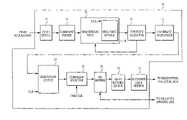
- FIG. 1shows a memory controller 10 in accordance with the present invention, and which includes an input queue 12 , a command parser 14 , a sequencing unit 16 , a sequence matrix 18 , a conflict detector 20 , a command sequencer 22 , an execution queue 24 , a command selector 26 , an input/output buffer 28 , a read return queue 30 , and a returned data buffer 32 .
- Memory access requestsenter the memory controller 10 and are received in input queue 12 on a first-in first-out basis.
- the received requestsare then sequentially processed by command parser 14 to obtain relevant information from each request signal, such as memory address (MA) data, a chip select (CS) command (indicating a requested memory bank to be accessed), a row address select (RAS) command, and a column address select (CAS) command, and a write enable (WE) state for indicating whether the request is a read or a write operation.
- MAmemory address
- CSchip select
- RASrow address select
- CAScolumn address select
- WEwrite enable
- the information obtainedis then provided to the sequencing unit 16 , which places the received memory access requests into a sequence matrix 18 in accordance with a clock signal received in the sequence matrix 18 . It is noted that upon startup of the process, the access requests are loaded into the matrix in the order in which they are received in the sequencing unit 16 .
- Conflict detector 20monitors the information in the sequence matrix 18 and checks for any conflicts or delays that may occur if the sequence of requests in the matrix were to be executed in the current order in the sequence matrix. Any conflict or delay detected by conflict detector 20 is reported back to sequencing unit 16 , which then rearranges the order of the requests in the matrix to minimize or eliminate the time the memory data bus is idle due to the identified conflicts or delays.
- Conflicts which may be detected by conflict detector 20include, but are not limited to, page conflicts and bank busy conditions in which a memory bank is busy performing another read or write operation, for example. Delays identified by the conflict detector are conditions which, while not necessarily a conflict with the execution of another memory access request, would require the performance of preparatory steps during which time the memory data bus is idle. Such delays include, for example, page conflicts, page misses, etc.
- both read and write type memory access requestsmay be re-ordered in the sequence matrix 18 .
- write requestsonly be rearranged if necessary to the extent that the re-ordered sequence does not create any addressing conflicts with earlier received requests in to the input queue or otherwise interfere with the data stored or to be stored in the relevant memory locations in connection with any other memory access requests in the matrix.
- the requests at the front of the sequenceare moved into the execution queue 24 , which serves as a transfer buffer where the rearranged requests await execution.
- the requestsmay be moved into the execution queue 24 either on a continuous basis in accordance with a clock signal, in batches of a predetermined number of access requests, or based on a predetermined cumulative size of the requests.
- the clock (CLK) for the execution queue 24is the same clock (CLK) guiding the loading of sequence matrix 18 .
- Command sequencer 22arranges the various commands associated with each request transferred to execution queue 24 from the sequence matrix 18 , as it may be necessary to insert and/or temporally separate data control commands from the read or write command of a particular memory access request. For example, if a read or write request sent to execution queue 24 requires a precharging and/or activation operation, a data control command to initiate the precharging and/or activation operation is placed in the execution queue ahead of the relevant read or write operation, with at least one other read or write command associated with a different access request positioned between the precharge and/or activate command and the associated read or write command.
- An advantage of the present inventionis realized by separating the read or write commands from such data control commands in this manner. Specifically, in the above example, the precharge and/or activation operation in the above example can be performed while the read or write command for another memory access request can be immediately executed. Thus, the memory data bus does not have to be idle during the time the pre-charge and/or activation operation is perfomed.
- each read requestWhen each read request is transferred to the execution queue, a tag is temporarily added to the data control commands for that request, for identifying the original relative placement of the each request as received in the input queue 12 .
- each read requestmay be assigned a respective buffer location in a read buffer 32 , which will be described in more detail later.
- command select clock (CMD CLK) signal fed into command selector 26one or more memory access requests from the front of the execution queue 24 is (are) selected for execution in the appropriate DRAM bank(s). For example, if the command select clock signal is four times the speed of the clock speed at which requests are loaded into sequence matrix 18 , then four access requests are removed from execution queue 24 for each clock signal of queue 24 . In this case, command selector 26 regulates the request selection process so that the four access requests which are all selected at one time from queue 24 are executed at even intervals. If the commands are selected from the execution queue for execution at the same clock speed at which new requests are entered into the sequence matrix 18 , then command selector 26 may be omitted from memory controller 10 .
- CMD CLKcommand select clock
- I/O buffer 28is a transition buffer used during the read or write operation specified in each access request. If a current access request to be executed is a write operation, the data to be written into the selected memory cell is temporarily written into I/O buffer 28 . Similarly, data read from a selected memory cell in a read operation is temporarily stored in I/O buffer 28 .
- each read requestUpon execution of the requested memory access, each read request is placed into a read return queue 30 .
- Read return queue 30manages the requested data read from the DRAM upon execution of the read requests, and returns the requested data to the respective requestors in the order in which they were received in the input queue. Data read from the DRAM is either transferred directly to the requestor or is placed into returned data buffer 32 , depending on the tag or assigned buffer location associated with the returned request data.
- the executed read requestis returned to the read request queue 30 , with the data obtained by the request being temporarily held in I/O buffer 28 (step 100 ). If the read request queue 30 determines at step 110 that the returning read request is associated with the most current tag or assigned buffer location, the data obtained by that request is returned to the requestor at step 120 , and the current tag/buffer location information is updated at step 130 .
- a tag or buffer locationis “current” if it is assigned to or associated with the read request having the longest latency in the memory controller 10 .
- Read return queue 30may keep track of the most current tag or buffer location, for example, by incrementing a count value which represents the current tag or buffer location each time a returned data is transferred to its requestor.
- the datais placed into the read data buffer 32 (step 140 ) until the associated tag or buffer location becomes current.
- the read return queue 30determines whether or not returned data corresponding to the current tag or buffer location can be found in the returned data buffer 32 . If “yes,” the process returns to step 120 , where the current returned data is transferred to the requestor of that data, and the current tag or buffer location is again updated in step 130 . If returned data corresponding to the current tag or buffer location is not found in the buffer 32 , the process returns to step 100 to receive the returned data obtained by the execution of the next read request in the execution queue. Due to this process shown in FIG. 2 , the read data is returned to the respective requestors in the order in which the requests were received into the input queue 12 .
- tagsare used to indicate the originally received order of the read requests, the tags are temporarily inserted among the data control commands of each request, but are not included in the read data returned to the requestors.
- the functions of the read return queue 30 and of the returned data buffer 32are performed according to a clock speed corresponding to the clock speed of the DRAM or an integral multiple thereof.
- returned read requests and returned data received in the read return queue 30 and returned data buffer 32can be coordinated with the updating of the current tag/buffer location and the transferring of the returned data, respectively.
- a first embodiment of a conflict re-ordering process which the sequencing unit 16 may use to reschedule a memory access request due to a detected conflict or delaywill be described with reference to the flowchart shown in FIG. 3
- the last memory access request to be parsedis placed in the sequence matrix 18 .
- the status of the memory bank desired to be accessedis checked to determine if any conflicts or delays would occur if the newly arrived memory access request is executed at its present position in the sequence matrix 18 .
- sequencing unit 16determines at step 240 whether a more suitable timing position can be found among the sequence of memory access requests ahead of its current position. Specifically, sequencing unit 16 first determines whether any unresolved conflicts or delays are present in the sequence ahead of the new access request, and if so, whether or not the new access request can be performed during that time without conflict. If there are no pending conflicts or delays, sequencing unit 16 checks whether the new access request may be rescheduled at any point in the matrix without causing any new conflicts or delays among the previously scheduled requests. If not, the process is redirected to step 230 , whereupon the new access request is left at the end of the current timing sequence with the unresolved condition. If a suitable timing position can be found ahead in the sequence, the newly arrived request is inserted into sequence at that position (step 250 ). The process is then returned to step 200 to be repeated for the next incoming memory access request.
- the conflict detector 20next determines at step 220 whether any unresolved conflicts or delays are present in the timing matrix ahead of the current position of the newly arrived request. If an unresolved conflict or delay is found, the process is redirected to step 240 discussed above. If no existing conflicts are found, the sequencing unit 16 leaves the request in its current position in sequence matrix 18 at step 230 , and then returns to step 200 to repeat the process for the next incoming memory access request.
- any unresolved conflicts or delaysmay or may not be later resolved with the arrival of a new access request with a subsequent iteration of the sequencing unit 16 . If no suitable request arrives to alleviate the conflict or delay, the memory access requests will continue to be processed in the designated order, but there will be some inefficiency in utilization of the memory data bus line due to the unresolved conflict(s) or unmitigated delay(s).
- a second embodiment of the conflict re-ordering process performed by sequencing unit 16is illustrated in the flowchart shown in FIG. 4 .
- the access request next in line in the sequence matrixis moved into the first location of the sequence matrix at step 300 .
- conflict detector 20determines whether a conflict or delay is present with respect to the access request at the head of the sequence matrix (i.e., the earliest one in among the requests in the matrix). If no conflict is found, the access request is passed onto the execution queue 24 at step 320 , and the process returns to step 300 .
- step 310the conflict detector 20 turns its attention to the next access request in the sequence matrix, and determines at step 330 whether or not that request can be performed at that time position without any conflicts. If no conflicts or delays would be created by scheduling that access request at that time position, the request is sent to the execution queue 24 at step 320 , and the process returns to step 300 . If a conflict or delay is found, the process repeats step 330 until a request is found which may be suitably executed at that time position.
- the rejected requestsremain in their current position in the sequence until a suitable time slot is found for the request.
- no memory accesswill be sent to the execution queue 24 with a conflict or delay condition.
- each requestis given priority based on latency, and will be executed at the earliest possible time slot in which no conflict condition is created by the timing of that request.
- step 420is executed in which the request having the conflict or delay is sent to the back of the sequence.
- conflict detector 20moves to the next access request in line to determine if any conflicts or delays are found with respect to that request (step 430 ). If no conflicts or delays are detected, the request is sent to the execution queue 24 , similarly to the process shown in FIG. 4 . If a conflict or delay is detected, the process returns to step 420 .
- FIG. 6a timing chart is shown illustrating the result obtained upon the operation of the present invention.
- read requests RD 0 , RD 1 , and RD 2are received in the input queue in the order as listed.
- RD 1 and RD 2are both page hits in other memory banks.
- the requestshave been rearranged so that while the precharge operation is being performed for RD 0 , read memory accesses for RD 1 and RD 2 are executed. Rearranging the commands in this manner minimizes the time that the memory data bus would have been idle while waiting for the precharge operation for RD 0 to finish executing, thus resulting in a more efficient utilization of the memory data bus.
- the activation operation for RD 0is performed, and then the read access command for RD 0 is performed.
- the read data “1111” and “2222”are transferred to the returned data buffer in the order the read operations are executed. After the “0000” data is obtained from the appropriate memory cell, however, the data is returned first to the requestor of RD 0 . Then, the data “1111” and “2222” are returned to their respective requestors, in that order.
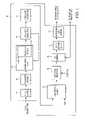
- FIG. 7illustrates an exemplary processing system 900 which may utilize the memory controller 10 of the present invention.
- the processing system 900includes one or more processors 901 coupled to a local bus 904 .
- Memory controller 10 and a primary bus bridge 903are also coupled the local bus 904 .
- the processing system 900may include multiple memory controllers 10 and/or multiple primary bus bridges 903 .
- the memory controller 10 and the primary bus bridge 903may be integrated as a single device 906 .
- the memory controller 10is also coupled to one or more memory data buses 907 .
- Each memory busaccepts memory components 908 which include at least one memory device 902 .
- the memory components 908may be formed as a memory card or a memory module. Examples of memory modules usable in the system 900 include single inline memory modules (SIMMs) and dual inline memory modules (DIMMs).
- the memory components 908may include one or more additional devices 909 .
- the additional device 909might be a configuration memory, such as a serial presence detect (SPD) memory.
- SPDserial presence detect
- the memory controller 10may also be coupled to a cache memory 905 .
- the cache memory 905may be the only cache memory in the processing system.
- processors 901may also include cache memories, which may form a cache hierarchy with cache memory 905 .
- the processing system 900include peripherals or controllers which are bus masters or which support direct memory access (DMA), the memory controller 10 may implement a cache coherency protocol. If the memory controller 10 is coupled to a plurality of memory buses 907 , each memory bus 907 may be operated in parallel, or different address ranges may be mapped to different memory buses 907 .
- the primary bus bridge 903is coupled to at least one peripheral bus 910 .
- Various devicessuch as peripherals or additional bus bridges may be coupled to the peripheral bus 910 . These devices may include a storage controller 911 , an miscellaneous I/O device 914 , a secondary bus bridge 915 , a multimedia processor 918 , and an legacy device interface 920 .
- the primary bus bridge 903may also coupled to one or more special purpose high speed ports 922 . In a personal computer, for example, the special purpose port might be the Accelerated Graphics Port (AGP), used to couple a high performance video card to the processing system 900 .
- AGPAccelerated Graphics Port
- the storage controller 911couples one or more storage devices 913 , via a storage bus 912 , to the peripheral bus 910 .
- the storage controller 911may be a SCSI controller and storage devices 913 may be SCSI discs.
- the I/O device 914may be any sort of peripheral.
- the I/O device 914may be an local area network interface, such as an Ethernet card.
- the secondary bus bridgemay be used to interface additional devices via another bus to the processing system.
- the secondary bus bridgemay be an universal serial port (USB) controller used to couple USB devices 917 via to the processing system 900 .
- the multimedia processor 918may be a sound card, a video capture card, or any other type of media interface, which may also be coupled to one additional devices such as speakers 919 .
- the legacy device interface 920is used to couple legacy devices, for example, older styled keyboards and mice, to the processing system 900 .
- FIG. 7illustrates a processing architecture especially suitable for a general purpose computer, such as a personal computer or a workstation, it should be recognized that well known modifications can be made to configure the processing system 900 to become more suitable for use in a variety of applications. For example, many electronic devices which require processing may be implemented using a simpler architecture which relies on a CPU 901 coupled to memory components 908 and/or memory devices 902 .
- These electronic devicesmay include, but are not limited to audio/video processors and recorders, gaming consoles, digital television sets, wired or wireless telephones, navigation devices (including system based on the global positioning system (GPS) and/or inertial navigation), and digital cameras and/or recorders.
- the modificationsmay include, for example, elimination of unnecessary components, addition of specialized devices or circuits, and/or integration of a plurality of devices.
Landscapes
- Engineering & Computer Science (AREA)
- Theoretical Computer Science (AREA)
- Physics & Mathematics (AREA)
- General Engineering & Computer Science (AREA)
- General Physics & Mathematics (AREA)
- Human Computer Interaction (AREA)
- Computer Security & Cryptography (AREA)
- Memory System (AREA)
- Multi Processors (AREA)
- Dram (AREA)
- Magnetic Resonance Imaging Apparatus (AREA)
- Advance Control (AREA)
- Apparatus For Radiation Diagnosis (AREA)
- Stabilization Of Oscillater, Synchronisation, Frequency Synthesizers (AREA)
- Electrotherapy Devices (AREA)
- Processing Of Color Television Signals (AREA)
Abstract
Description
Claims (54)
Priority Applications (14)
| Application Number | Priority Date | Filing Date | Title |
|---|---|---|---|
| US10/143,896US7149857B2 (en) | 2002-05-14 | 2002-05-14 | Out of order DRAM sequencer |
| AT03753034TATE456094T1 (en) | 2002-05-14 | 2003-05-14 | NON-SEQUENTIAL DRAM SEQUENCE CONTROL |
| JP2004505842AJP2005525652A (en) | 2002-05-14 | 2003-05-14 | Out-of-order DRAM sequencer |
| PCT/US2003/015184WO2003098392A2 (en) | 2002-05-14 | 2003-05-14 | Out of order dram sequencer |
| EP03753034AEP1540485B1 (en) | 2002-05-14 | 2003-05-14 | Out of order dram sequencer |
| KR10-2004-7018434AKR20050005481A (en) | 2002-05-14 | 2003-05-14 | Out of order dram sequencer |
| CNB038167735ACN100527107C (en) | 2002-05-14 | 2003-05-14 | Out-of-order DRAM sequencer |
| DE60331081TDE60331081D1 (en) | 2002-05-14 | 2003-05-14 | NON-SEQUENTIAL DRAM FOLLOW CONTROL |
| KR1020067017435AKR100724557B1 (en) | 2002-05-14 | 2003-05-14 | Out of order dram sequencer |
| AU2003232136AAU2003232136A1 (en) | 2002-05-14 | 2003-05-14 | Out of order dram sequencer |
| US11/604,906US7620789B2 (en) | 2002-05-14 | 2006-11-28 | Out of order DRAM sequencer |
| JP2008140086AJP4742116B2 (en) | 2002-05-14 | 2008-05-28 | Out-of-order DRAM sequencer |
| US12/604,579US8639902B2 (en) | 2002-05-14 | 2009-10-23 | Methods for sequencing memory access requests |
| US14/165,423US9904489B2 (en) | 2002-05-14 | 2014-01-27 | Processing systems, memory controllers and methods for controlling memory access operations |
Applications Claiming Priority (1)
| Application Number | Priority Date | Filing Date | Title |
|---|---|---|---|
| US10/143,896US7149857B2 (en) | 2002-05-14 | 2002-05-14 | Out of order DRAM sequencer |
Related Child Applications (1)
| Application Number | Title | Priority Date | Filing Date |
|---|---|---|---|
| US11/604,906ContinuationUS7620789B2 (en) | 2002-05-14 | 2006-11-28 | Out of order DRAM sequencer |
Publications (2)
| Publication Number | Publication Date |
|---|---|
| US20030217239A1 US20030217239A1 (en) | 2003-11-20 |
| US7149857B2true US7149857B2 (en) | 2006-12-12 |
Family
ID=29418478
Family Applications (4)
| Application Number | Title | Priority Date | Filing Date |
|---|---|---|---|
| US10/143,896Expired - LifetimeUS7149857B2 (en) | 2002-05-14 | 2002-05-14 | Out of order DRAM sequencer |
| US11/604,906Expired - LifetimeUS7620789B2 (en) | 2002-05-14 | 2006-11-28 | Out of order DRAM sequencer |
| US12/604,579Expired - LifetimeUS8639902B2 (en) | 2002-05-14 | 2009-10-23 | Methods for sequencing memory access requests |
| US14/165,423Expired - LifetimeUS9904489B2 (en) | 2002-05-14 | 2014-01-27 | Processing systems, memory controllers and methods for controlling memory access operations |
Family Applications After (3)
| Application Number | Title | Priority Date | Filing Date |
|---|---|---|---|
| US11/604,906Expired - LifetimeUS7620789B2 (en) | 2002-05-14 | 2006-11-28 | Out of order DRAM sequencer |
| US12/604,579Expired - LifetimeUS8639902B2 (en) | 2002-05-14 | 2009-10-23 | Methods for sequencing memory access requests |
| US14/165,423Expired - LifetimeUS9904489B2 (en) | 2002-05-14 | 2014-01-27 | Processing systems, memory controllers and methods for controlling memory access operations |
Country Status (9)
| Country | Link |
|---|---|
| US (4) | US7149857B2 (en) |
| EP (1) | EP1540485B1 (en) |
| JP (2) | JP2005525652A (en) |
| KR (2) | KR20050005481A (en) |
| CN (1) | CN100527107C (en) |
| AT (1) | ATE456094T1 (en) |
| AU (1) | AU2003232136A1 (en) |
| DE (1) | DE60331081D1 (en) |
| WO (1) | WO2003098392A2 (en) |
Cited By (10)
| Publication number | Priority date | Publication date | Assignee | Title |
|---|---|---|---|---|
| US7418706B1 (en)* | 2003-05-08 | 2008-08-26 | Teradota Us, Inc. | Rescheduling table scan transactions |
| US20080215783A1 (en)* | 2007-03-01 | 2008-09-04 | Allen James J | Structure for data bus bandwidth scheduling in an fbdimm memory system operating in variable latency mode |
| US20090055580A1 (en)* | 2007-08-21 | 2009-02-26 | Microsoft Corporation | Multi-level dram controller to manage access to dram |
| US20090150624A1 (en)* | 2007-11-15 | 2009-06-11 | Micron Technology, Inc. | System, apparatus, and method for modifying the order of memory accesseses |
| US20090216962A1 (en)* | 2008-02-26 | 2009-08-27 | Microsoft Corporation | Prioritization of multiple concurrent threads for scheduling requests to shared memory |
| US20110066821A1 (en)* | 2008-05-21 | 2011-03-17 | Nxp B.V. | data handling system comprising a rearrangement network |
| USRE44402E1 (en)* | 2005-03-09 | 2013-07-30 | Jinsalas Solutions, Llc | System and method for storing a sequential data stream |
| US8601205B1 (en)* | 2008-12-31 | 2013-12-03 | Synopsys, Inc. | Dynamic random access memory controller |
| EP2992437A4 (en)* | 2013-04-30 | 2017-01-11 | Hewlett-Packard Enterprise Development LP | Coalescing memory access requests |
| US20230362280A1 (en)* | 2018-02-12 | 2023-11-09 | Micron Technology, Inc. | Optimization of data access and communication in memory systems |
Families Citing this family (98)
| Publication number | Priority date | Publication date | Assignee | Title |
|---|---|---|---|---|
| US6694490B2 (en)* | 2002-07-10 | 2004-02-17 | Hewlett-Packard Development Company, L.P. | DIMM and method for producing a DIMM |
| US7399043B2 (en)* | 2002-12-02 | 2008-07-15 | Silverbrook Research Pty Ltd | Compensation for uneven printhead module lengths in a multi-module printhead |
| US7240141B2 (en)* | 2004-04-09 | 2007-07-03 | Broadcom Corporation | Programmable inter-virtual channel and intra-virtual channel instructions issuing rules for an I/O bus of a system-on-a-chip processor |
| US20060026371A1 (en)* | 2004-07-30 | 2006-02-02 | Chrysos George Z | Method and apparatus for implementing memory order models with order vectors |
| US9286198B2 (en) | 2005-04-21 | 2016-03-15 | Violin Memory | Method and system for storage of data in non-volatile media |
| US8200887B2 (en) | 2007-03-29 | 2012-06-12 | Violin Memory, Inc. | Memory management system and method |
| US8452929B2 (en)* | 2005-04-21 | 2013-05-28 | Violin Memory Inc. | Method and system for storage of data in non-volatile media |
| US9384818B2 (en) | 2005-04-21 | 2016-07-05 | Violin Memory | Memory power management |
| US8028186B2 (en) | 2006-10-23 | 2011-09-27 | Violin Memory, Inc. | Skew management in an interconnection system |
| US8019938B2 (en) | 2006-12-06 | 2011-09-13 | Fusion-I0, Inc. | Apparatus, system, and method for solid-state storage as cache for high-capacity, non-volatile storage |
| CN100565485C (en)* | 2006-12-21 | 2009-12-02 | 扬智科技股份有限公司 | Method and device for reading external memory |
| US8265169B2 (en)* | 2006-12-29 | 2012-09-11 | Intel Corporation | Video block memory read request translation and tagging |
| US9632870B2 (en) | 2007-03-29 | 2017-04-25 | Violin Memory, Inc. | Memory system with multiple striping of raid groups and method for performing the same |
| US11010076B2 (en) | 2007-03-29 | 2021-05-18 | Violin Systems Llc | Memory system with multiple striping of raid groups and method for performing the same |
| US8015375B1 (en) | 2007-03-30 | 2011-09-06 | Emc Corporation | Methods, systems, and computer program products for parallel processing and saving tracking information for multiple write requests in a data replication environment including multiple storage devices |
| US7996599B2 (en)* | 2007-04-25 | 2011-08-09 | Apple Inc. | Command resequencing in memory operations |
| US7925796B1 (en) | 2007-05-03 | 2011-04-12 | Emc Corporation | Methods, systems, and computer program products for performing an input/output (I/O) operation that includes a virtual drain |
| US8145976B1 (en) | 2007-05-14 | 2012-03-27 | Marvell International Ltd. | Error correcting |
| US7836226B2 (en) | 2007-12-06 | 2010-11-16 | Fusion-Io, Inc. | Apparatus, system, and method for coordinating storage requests in a multi-processor/multi-thread environment |
| US8156415B1 (en)* | 2007-12-26 | 2012-04-10 | Marvell International Ltd. | Method and system for command queuing in disk drives |
| CN101520749B (en)* | 2008-02-29 | 2012-08-29 | 瑞昱半导体股份有限公司 | Methods of managing memory |
| US8370717B1 (en) | 2008-04-08 | 2013-02-05 | Marvell International Ltd. | Method and apparatus for flexible buffers in an XOR engine |
| CN101727398B (en)* | 2008-10-31 | 2012-07-11 | 西安奇维测控科技有限公司 | Method for realizing management data storage and restoration of flash memory controller through information serialization |
| JP2010182092A (en)* | 2009-02-05 | 2010-08-19 | Mitsubishi Electric Corp | Bus device |
| KR101581679B1 (en)* | 2009-03-18 | 2015-12-31 | 삼성전자주식회사 | Storage device and method for managing buffer memory of storage device |
| US8199759B2 (en)* | 2009-05-29 | 2012-06-12 | Intel Corporation | Method and apparatus for enabling ID based streams over PCI express |
| CN102576330B (en) | 2009-06-12 | 2015-01-28 | 提琴存储器公司 | Storage system with persistent garbage collection mechanism |
| US8650438B2 (en)* | 2009-08-11 | 2014-02-11 | Marvell World Trade Ltd. | Controller for reading data from non-volatile memory |
| US8644140B2 (en)* | 2009-09-09 | 2014-02-04 | Mellanox Technologies Ltd. | Data switch with shared port buffers |
| CN102253917B (en)* | 2010-05-19 | 2014-03-19 | 联芯科技有限公司 | Serial peripheral interface (SPI) controller and data sending method |
| KR101121902B1 (en)* | 2010-06-22 | 2012-03-20 | 성균관대학교산학협력단 | Transactional memory system and method for tracking modified memory address |
| US9021192B1 (en)* | 2010-09-21 | 2015-04-28 | Western Digital Technologies, Inc. | System and method for enhancing processing of memory access requests |
| US8699491B2 (en)* | 2011-07-25 | 2014-04-15 | Mellanox Technologies Ltd. | Network element with shared buffers |
| JP5704012B2 (en)* | 2011-08-01 | 2015-04-22 | 富士通セミコンダクター株式会社 | Processor and control method of processor |
| KR101292309B1 (en)* | 2011-12-27 | 2013-07-31 | 숭실대학교산학협력단 | Semiconductor chip and control method of memory, and recording medium storing program for executing method of the same in computer |
| CN102567246B (en)* | 2011-12-29 | 2014-08-13 | 中国人民解放军国防科学技术大学 | NAND flash memory controller supporting operation out-of-order execution |
| KR101721273B1 (en)* | 2012-01-16 | 2017-03-29 | 한국전자통신연구원 | Non - sequential data transmission apparatus and method using sdio interface |
| US20130185491A1 (en)* | 2012-01-17 | 2013-07-18 | Skymedi Corporation | Memory controller and a method thereof |
| US9251086B2 (en) | 2012-01-24 | 2016-02-02 | SanDisk Technologies, Inc. | Apparatus, system, and method for managing a cache |
| US9348775B2 (en) | 2012-03-16 | 2016-05-24 | Analog Devices, Inc. | Out-of-order execution of bus transactions |
| US8775762B2 (en)* | 2012-05-07 | 2014-07-08 | Advanced Micro Devices, Inc. | Method and apparatus for batching memory requests |
| KR20140028618A (en)* | 2012-08-29 | 2014-03-10 | 삼성전자주식회사 | Memory device for reducimg write fail, system includinmg tha same, and method there-of |
| US9047092B2 (en)* | 2012-12-21 | 2015-06-02 | Arm Limited | Resource management within a load store unit |
| US9582440B2 (en) | 2013-02-10 | 2017-02-28 | Mellanox Technologies Ltd. | Credit based low-latency arbitration with data transfer |
| US8989011B2 (en) | 2013-03-14 | 2015-03-24 | Mellanox Technologies Ltd. | Communication over multiple virtual lanes using a shared buffer |
| KR102120823B1 (en) | 2013-08-14 | 2020-06-09 | 삼성전자주식회사 | Method of controlling read sequence of nov-volatile memory device and memory system performing the same |
| US9641465B1 (en) | 2013-08-22 | 2017-05-02 | Mellanox Technologies, Ltd | Packet switch with reduced latency |
| US9548960B2 (en) | 2013-10-06 | 2017-01-17 | Mellanox Technologies Ltd. | Simplified packet routing |
| US20150199134A1 (en)* | 2014-01-10 | 2015-07-16 | Qualcomm Incorporated | System and method for resolving dram page conflicts based on memory access patterns |
| US9325641B2 (en) | 2014-03-13 | 2016-04-26 | Mellanox Technologies Ltd. | Buffering schemes for communication over long haul links |
| US9875185B2 (en) | 2014-07-09 | 2018-01-23 | Intel Corporation | Memory sequencing with coherent and non-coherent sub-systems |
| US9584429B2 (en) | 2014-07-21 | 2017-02-28 | Mellanox Technologies Ltd. | Credit based flow control for long-haul links |
| US9740411B2 (en)* | 2014-09-04 | 2017-08-22 | National Instruments Corporation | Configuring circuitry with memory access constraints for a program |
| GB2550829B (en)* | 2014-10-14 | 2021-09-22 | Advanced Risc Mach Ltd | Transaction response modification within interconnect circuitry |
| KR20160049200A (en)* | 2014-10-27 | 2016-05-09 | 삼성전자주식회사 | Method for operating data storage device, mobile computing device having the same, and method of the mobile computing device |
| CN104375963B (en)* | 2014-11-28 | 2019-03-15 | 上海兆芯集成电路有限公司 | Cache coherency-based control system and method |
| US9740646B2 (en)* | 2014-12-20 | 2017-08-22 | Intel Corporation | Early identification in transactional buffered memory |
| CN106164888A (en)* | 2015-02-26 | 2016-11-23 | 斯特拉托斯卡莱有限公司 | An ordering scheme for network and storage I/O requests to minimize workload idle time and inter-workload interference |
| GB2539435B8 (en)* | 2015-06-16 | 2018-02-21 | Advanced Risc Mach Ltd | Data processing memory access control, in which an owning process for a region of memory is specified independently of privilege level |
| JP2017027479A (en)* | 2015-07-24 | 2017-02-02 | 富士通株式会社 | Data reading method and information processing system |
| CN106469126B (en)* | 2015-08-12 | 2020-07-07 | 北京忆恒创源科技有限公司 | Method for processing IO request and storage controller thereof |
| JP2017204170A (en)* | 2016-05-12 | 2017-11-16 | キヤノン株式会社 | Image processing device and image processing method |
| GB2551351B (en)* | 2016-06-14 | 2019-05-08 | Imagination Tech Ltd | Executing memory requests out of order |
| US10353819B2 (en)* | 2016-06-24 | 2019-07-16 | Qualcomm Incorporated | Next line prefetchers employing initial high prefetch prediction confidence states for throttling next line prefetches in a processor-based system |
| WO2018003244A1 (en)* | 2016-06-29 | 2018-01-04 | ソニー株式会社 | Memory controller, memory system, and information processing system |
| KR20180069960A (en)* | 2016-12-15 | 2018-06-26 | 에스케이하이닉스 주식회사 | Memory system and method thereof |
| KR102687676B1 (en)* | 2017-02-02 | 2024-07-23 | 에스케이하이닉스 주식회사 | Data storage device and operating method thereof |
| JP2018205859A (en)* | 2017-05-31 | 2018-12-27 | キヤノン株式会社 | Memory controller and control method thereof |
| CN107770620B (en)* | 2017-09-21 | 2020-10-30 | 广州视源电子科技股份有限公司 | Request information response method, system and readable storage medium |
| US10419265B2 (en) | 2017-11-29 | 2019-09-17 | Bank Of America Corporation | Request processing system using a combining engine |
| US10425456B2 (en) | 2017-11-29 | 2019-09-24 | Bank Of America Corporation | Request processing system using a splitting engine |
| CN108335719A (en)* | 2018-02-24 | 2018-07-27 | 上海兆芯集成电路有限公司 | Capability evaluating device and performance estimating method |
| US11874782B1 (en)* | 2018-07-20 | 2024-01-16 | Robert Gezelter | Fast mass storage access for digital computers |
| US11099778B2 (en)* | 2018-08-08 | 2021-08-24 | Micron Technology, Inc. | Controller command scheduling in a memory system to increase command bus utilization |
| CN109683963A (en)* | 2018-12-10 | 2019-04-26 | 深圳忆联信息系统有限公司 | The output method that reorders, device and computer equipment based on more order inputs |
| TWI701554B (en)* | 2018-12-13 | 2020-08-11 | 英屬維京群島商鯨鏈先進股份有限公司 | Circuit system adapted to hash algorithm |
| US10951549B2 (en) | 2019-03-07 | 2021-03-16 | Mellanox Technologies Tlv Ltd. | Reusing switch ports for external buffer network |
| CN110046053B (en) | 2019-04-19 | 2021-11-12 | 上海兆芯集成电路有限公司 | Processing system for distributing tasks and access method thereof |
| CN110083388B (en)* | 2019-04-19 | 2021-11-12 | 上海兆芯集成电路有限公司 | Processing system for scheduling and access method thereof |
| CN110032453B (en) | 2019-04-19 | 2022-05-03 | 上海兆芯集成电路有限公司 | Processing system for task scheduling and distribution and acceleration method thereof |
| CN110058931B (en) | 2019-04-19 | 2022-03-22 | 上海兆芯集成电路有限公司 | Processing system for task scheduling and acceleration method thereof |
| CN110083387B (en) | 2019-04-19 | 2021-11-12 | 上海兆芯集成电路有限公司 | Processing system using polling mechanism and access method thereof |
| US11093404B2 (en)* | 2019-10-14 | 2021-08-17 | EMC IP Holding Company LLC | Efficient pre-fetching on a storage system |
| GB2588618B (en)* | 2019-10-29 | 2022-04-20 | Advanced Risc Mach Ltd | Methods and apparatus for issuing memory access commands |
| US20210200694A1 (en)* | 2019-12-27 | 2021-07-01 | Advanced Micro Devices, Inc. | Staging buffer arbitration |
| US11481152B2 (en)* | 2019-12-30 | 2022-10-25 | Micron Technology, Inc. | Execution of commands addressed to a logical block |
| US11470010B2 (en) | 2020-02-06 | 2022-10-11 | Mellanox Technologies, Ltd. | Head-of-queue blocking for multiple lossless queues |
| CN113377277B (en)* | 2020-03-09 | 2024-08-16 | 伊姆西Ip控股有限责任公司 | Method, apparatus and computer program product for managing memory |
| US11995719B1 (en) | 2020-09-21 | 2024-05-28 | Cboe Exchange, Inc. | Message randomization and delay based on order type in an electronic trading system |
| US11727421B1 (en) | 2020-09-21 | 2023-08-15 | Cboe Exchange, Inc | System and method for implementing a system execution delay in response to liquidity removal for resting orders |
| US11558316B2 (en) | 2021-02-15 | 2023-01-17 | Mellanox Technologies, Ltd. | Zero-copy buffering of traffic of long-haul links |
| WO2022174367A1 (en)* | 2021-02-18 | 2022-08-25 | Micron Technology, Inc. | Improved implicit ordered command handling |
| JP7614928B2 (en)* | 2021-04-26 | 2025-01-16 | キヤノン株式会社 | MEMORY CONTROLLER, METHOD FOR CONTROLLING MEMORY CONTROLLER, AND PROGRAM - Patent application |
| JP7647472B2 (en)* | 2021-09-22 | 2025-03-18 | 富士通株式会社 | Processing device and memory access method |
| CN114036096B (en)* | 2021-11-04 | 2024-05-03 | 珠海一微半导体股份有限公司 | Read controller based on bus interface |
| US11973696B2 (en) | 2022-01-31 | 2024-04-30 | Mellanox Technologies, Ltd. | Allocation of shared reserve memory to queues in a network device |
| US12375404B2 (en) | 2022-08-25 | 2025-07-29 | Mellanox Technologies, Ltd | Flow-based congestion control |
| US12353713B2 (en) | 2023-03-10 | 2025-07-08 | SanDisk Technologies, Inc. | Memory controller with common request buffer |
Citations (29)
| Publication number | Priority date | Publication date | Assignee | Title |
|---|---|---|---|---|
| US5388247A (en) | 1993-05-14 | 1995-02-07 | Digital Equipment Corporation | History buffer control to reduce unnecessary allocations in a memory stream buffer |
| US5461718A (en) | 1992-04-24 | 1995-10-24 | Digital Equipment Corporation | System for sequential read of memory stream buffer detecting page mode cycles availability fetching data into a selected FIFO, and sending data without aceessing memory |
| US5522059A (en) | 1992-11-26 | 1996-05-28 | Nec Corporation | Apparatus for multiport memory access control unit with plurality of bank busy state check mechanisms employing address decoding and coincidence detection schemes |
| US5537572A (en) | 1992-03-31 | 1996-07-16 | Vlsi Technology, Inc. | Cache controller and method for dumping contents of a cache directory and cache data random access memory (RAM) |
| US5630099A (en) | 1993-12-10 | 1997-05-13 | Advanced Micro Devices | Non-volatile memory array controller capable of controlling memory banks having variable bit widths |
| US5630096A (en) | 1995-05-10 | 1997-05-13 | Microunity Systems Engineering, Inc. | Controller for a synchronous DRAM that maximizes throughput by allowing memory requests and commands to be issued out of order |
| US5638374A (en)* | 1995-03-15 | 1997-06-10 | Hughes Electronics | Enhanced transaction reservation |
| US5664153A (en) | 1993-04-21 | 1997-09-02 | Intel Corporation | Page open/close scheme based on high order address bit and likelihood of page access |
| US5701434A (en) | 1995-03-16 | 1997-12-23 | Hitachi, Ltd. | Interleave memory controller with a common access queue |
| US5819076A (en) | 1995-09-12 | 1998-10-06 | Micron Electronics, Inc. | Memory controller with low skew control signal |
| US5848025A (en) | 1997-06-30 | 1998-12-08 | Motorola, Inc. | Method and apparatus for controlling a memory device in a page mode |
| US5872822A (en) | 1995-10-26 | 1999-02-16 | Mcdata Corporation | Method and apparatus for memory sequencing |
| US5907863A (en) | 1996-08-16 | 1999-05-25 | Unisys Corporation | Memory control unit using preloaded values to generate optimal timing of memory control sequences between different memory segments |
| US5983325A (en) | 1997-12-09 | 1999-11-09 | Advanced Micro Devices, Inc. | Dataless touch to open a memory page |
| US6052134A (en) | 1997-12-22 | 2000-04-18 | Compaq Computer Corp. | Memory controller and method for dynamic page management |
| US6052756A (en) | 1998-01-23 | 2000-04-18 | Oki Electric Industry Co., Ltd. | Memory page management |
| US6061759A (en) | 1996-02-09 | 2000-05-09 | Apex Semiconductor, Inc. | Hidden precharge pseudo cache DRAM |
| US6181638B1 (en) | 1998-12-07 | 2001-01-30 | Micron Technology, Inc. | Method for receiving data from a synchronous random access memory |
| US6204864B1 (en) | 1995-06-07 | 2001-03-20 | Seiko Epson Corporation | Apparatus and method having improved memory controller request handler |
| US6212598B1 (en) | 1998-11-30 | 2001-04-03 | Micron Technology, Inc. | Controlling a paging policy based on a requestor characteristic |
| US6212611B1 (en)* | 1998-11-03 | 2001-04-03 | Intel Corporation | Method and apparatus for providing a pipelined memory controller |
| US6212231B1 (en) | 1996-12-25 | 2001-04-03 | Nec Corporation | Assign of pels of a macroblock for compression encoding to a memory sequence in one of banks of DRAM |
| US6275913B1 (en) | 1999-10-15 | 2001-08-14 | Micron Technology, Inc. | Method for preserving memory request ordering across multiple memory controllers |
| US6295592B1 (en) | 1998-07-31 | 2001-09-25 | Micron Technology, Inc. | Method of processing memory requests in a pipelined memory controller |
| US6295586B1 (en) | 1998-12-04 | 2001-09-25 | Advanced Micro Devices, Inc. | Queue based memory controller |
| US6330647B1 (en) | 1999-08-31 | 2001-12-11 | Micron Technology, Inc. | Memory bandwidth allocation based on access count priority scheme |
| US6330683B1 (en) | 1998-10-30 | 2001-12-11 | Micron Technology, Inc. | Method for aligning clock and data signals received from a RAM |
| US6385708B1 (en) | 1998-11-16 | 2002-05-07 | Infineon Technologies Ag | Using a timing-look-up-table and page timers to determine the time between two consecutive memory accesses |
| US6510474B1 (en)* | 1998-11-16 | 2003-01-21 | Infineon Technologies Ag | Methods and apparatus for re-reordering command and data packets in order to restore an original order of out-of-order memory requests |
Family Cites Families (9)
| Publication number | Priority date | Publication date | Assignee | Title |
|---|---|---|---|---|
| US3735354A (en) | 1972-04-07 | 1973-05-22 | Sperry Rand Corp | Multiplexed memory request interface |
| JP3157507B2 (en)* | 1990-03-14 | 2001-04-16 | 日本電気株式会社 | Data processing device |
| US6272600B1 (en)* | 1996-11-15 | 2001-08-07 | Hyundai Electronics America | Memory request reordering in a data processing system |
| US6434684B1 (en) | 1998-09-03 | 2002-08-13 | Micron Technology, Inc. | Method and apparatus for coupling signals across different clock domains, and memory device and computer system using same |
| US6389529B1 (en) | 1999-06-25 | 2002-05-14 | International Business Machines Corporation | Method for alternate preferred time delivery of load data |
| JP2001022529A (en)* | 1999-06-30 | 2001-01-26 | Internatl Business Mach Corp <Ibm> | Disk drive device and control method therefor |
| JP2001154913A (en)* | 1999-11-30 | 2001-06-08 | Hitachi Ltd | Main memory controller |
| US6735677B1 (en) | 2001-04-30 | 2004-05-11 | Lsi Logic Corporation | Parameterizable queued memory access system |
| US7242690B2 (en) | 2002-03-05 | 2007-07-10 | Hewlett-Packard Development Company, L.P. | System for performing input processing on a data packet |
- 2002
- 2002-05-14USUS10/143,896patent/US7149857B2/ennot_activeExpired - Lifetime
- 2003
- 2003-05-14ATAT03753034Tpatent/ATE456094T1/ennot_activeIP Right Cessation
- 2003-05-14WOPCT/US2003/015184patent/WO2003098392A2/enactiveApplication Filing
- 2003-05-14JPJP2004505842Apatent/JP2005525652A/ennot_activeWithdrawn
- 2003-05-14EPEP03753034Apatent/EP1540485B1/ennot_activeExpired - Lifetime
- 2003-05-14KRKR10-2004-7018434Apatent/KR20050005481A/ennot_activeCeased
- 2003-05-14DEDE60331081Tpatent/DE60331081D1/ennot_activeExpired - Lifetime
- 2003-05-14AUAU2003232136Apatent/AU2003232136A1/ennot_activeAbandoned
- 2003-05-14KRKR1020067017435Apatent/KR100724557B1/ennot_activeExpired - Lifetime
- 2003-05-14CNCNB038167735Apatent/CN100527107C/ennot_activeExpired - Lifetime
- 2006
- 2006-11-28USUS11/604,906patent/US7620789B2/ennot_activeExpired - Lifetime
- 2008
- 2008-05-28JPJP2008140086Apatent/JP4742116B2/ennot_activeExpired - Fee Related
- 2009
- 2009-10-23USUS12/604,579patent/US8639902B2/ennot_activeExpired - Lifetime
- 2014
- 2014-01-27USUS14/165,423patent/US9904489B2/ennot_activeExpired - Lifetime
Patent Citations (29)
| Publication number | Priority date | Publication date | Assignee | Title |
|---|---|---|---|---|
| US5537572A (en) | 1992-03-31 | 1996-07-16 | Vlsi Technology, Inc. | Cache controller and method for dumping contents of a cache directory and cache data random access memory (RAM) |
| US5461718A (en) | 1992-04-24 | 1995-10-24 | Digital Equipment Corporation | System for sequential read of memory stream buffer detecting page mode cycles availability fetching data into a selected FIFO, and sending data without aceessing memory |
| US5522059A (en) | 1992-11-26 | 1996-05-28 | Nec Corporation | Apparatus for multiport memory access control unit with plurality of bank busy state check mechanisms employing address decoding and coincidence detection schemes |
| US5664153A (en) | 1993-04-21 | 1997-09-02 | Intel Corporation | Page open/close scheme based on high order address bit and likelihood of page access |
| US5388247A (en) | 1993-05-14 | 1995-02-07 | Digital Equipment Corporation | History buffer control to reduce unnecessary allocations in a memory stream buffer |
| US5630099A (en) | 1993-12-10 | 1997-05-13 | Advanced Micro Devices | Non-volatile memory array controller capable of controlling memory banks having variable bit widths |
| US5638374A (en)* | 1995-03-15 | 1997-06-10 | Hughes Electronics | Enhanced transaction reservation |
| US5701434A (en) | 1995-03-16 | 1997-12-23 | Hitachi, Ltd. | Interleave memory controller with a common access queue |
| US5630096A (en) | 1995-05-10 | 1997-05-13 | Microunity Systems Engineering, Inc. | Controller for a synchronous DRAM that maximizes throughput by allowing memory requests and commands to be issued out of order |
| US6204864B1 (en) | 1995-06-07 | 2001-03-20 | Seiko Epson Corporation | Apparatus and method having improved memory controller request handler |
| US5819076A (en) | 1995-09-12 | 1998-10-06 | Micron Electronics, Inc. | Memory controller with low skew control signal |
| US5872822A (en) | 1995-10-26 | 1999-02-16 | Mcdata Corporation | Method and apparatus for memory sequencing |
| US6061759A (en) | 1996-02-09 | 2000-05-09 | Apex Semiconductor, Inc. | Hidden precharge pseudo cache DRAM |
| US5907863A (en) | 1996-08-16 | 1999-05-25 | Unisys Corporation | Memory control unit using preloaded values to generate optimal timing of memory control sequences between different memory segments |
| US6212231B1 (en) | 1996-12-25 | 2001-04-03 | Nec Corporation | Assign of pels of a macroblock for compression encoding to a memory sequence in one of banks of DRAM |
| US5848025A (en) | 1997-06-30 | 1998-12-08 | Motorola, Inc. | Method and apparatus for controlling a memory device in a page mode |
| US5983325A (en) | 1997-12-09 | 1999-11-09 | Advanced Micro Devices, Inc. | Dataless touch to open a memory page |
| US6052134A (en) | 1997-12-22 | 2000-04-18 | Compaq Computer Corp. | Memory controller and method for dynamic page management |
| US6052756A (en) | 1998-01-23 | 2000-04-18 | Oki Electric Industry Co., Ltd. | Memory page management |
| US6295592B1 (en) | 1998-07-31 | 2001-09-25 | Micron Technology, Inc. | Method of processing memory requests in a pipelined memory controller |
| US6330683B1 (en) | 1998-10-30 | 2001-12-11 | Micron Technology, Inc. | Method for aligning clock and data signals received from a RAM |
| US6212611B1 (en)* | 1998-11-03 | 2001-04-03 | Intel Corporation | Method and apparatus for providing a pipelined memory controller |
| US6385708B1 (en) | 1998-11-16 | 2002-05-07 | Infineon Technologies Ag | Using a timing-look-up-table and page timers to determine the time between two consecutive memory accesses |
| US6510474B1 (en)* | 1998-11-16 | 2003-01-21 | Infineon Technologies Ag | Methods and apparatus for re-reordering command and data packets in order to restore an original order of out-of-order memory requests |
| US6212598B1 (en) | 1998-11-30 | 2001-04-03 | Micron Technology, Inc. | Controlling a paging policy based on a requestor characteristic |
| US6295586B1 (en) | 1998-12-04 | 2001-09-25 | Advanced Micro Devices, Inc. | Queue based memory controller |
| US6181638B1 (en) | 1998-12-07 | 2001-01-30 | Micron Technology, Inc. | Method for receiving data from a synchronous random access memory |
| US6330647B1 (en) | 1999-08-31 | 2001-12-11 | Micron Technology, Inc. | Memory bandwidth allocation based on access count priority scheme |
| US6275913B1 (en) | 1999-10-15 | 2001-08-14 | Micron Technology, Inc. | Method for preserving memory request ordering across multiple memory controllers |
Cited By (18)
| Publication number | Priority date | Publication date | Assignee | Title |
|---|---|---|---|---|
| US7418706B1 (en)* | 2003-05-08 | 2008-08-26 | Teradota Us, Inc. | Rescheduling table scan transactions |
| USRE44402E1 (en)* | 2005-03-09 | 2013-07-30 | Jinsalas Solutions, Llc | System and method for storing a sequential data stream |
| US20080215783A1 (en)* | 2007-03-01 | 2008-09-04 | Allen James J | Structure for data bus bandwidth scheduling in an fbdimm memory system operating in variable latency mode |
| US8028257B2 (en)* | 2007-03-01 | 2011-09-27 | International Business Machines Corporation | Structure for data bus bandwidth scheduling in an FBDIMM memory system operating in variable latency mode |
| US8001338B2 (en) | 2007-08-21 | 2011-08-16 | Microsoft Corporation | Multi-level DRAM controller to manage access to DRAM |
| US20090055580A1 (en)* | 2007-08-21 | 2009-02-26 | Microsoft Corporation | Multi-level dram controller to manage access to dram |
| US8180974B2 (en) | 2007-11-15 | 2012-05-15 | Micron Technology, Inc. | System, apparatus, and method for modifying the order of memory accesses |
| US20110099341A1 (en)* | 2007-11-15 | 2011-04-28 | Micron Technology, Inc. | System, apparatus, and method for modifying the order of memory accesses |
| US7870351B2 (en) | 2007-11-15 | 2011-01-11 | Micron Technology, Inc. | System, apparatus, and method for modifying the order of memory accesses |
| US20090150624A1 (en)* | 2007-11-15 | 2009-06-11 | Micron Technology, Inc. | System, apparatus, and method for modifying the order of memory accesseses |
| US20090217273A1 (en)* | 2008-02-26 | 2009-08-27 | Microsoft Corporation | Controlling interference in shared memory systems using parallelism-aware batch scheduling |
| US8180975B2 (en)* | 2008-02-26 | 2012-05-15 | Microsoft Corporation | Controlling interference in shared memory systems using parallelism-aware batch scheduling |
| US20090216962A1 (en)* | 2008-02-26 | 2009-08-27 | Microsoft Corporation | Prioritization of multiple concurrent threads for scheduling requests to shared memory |
| US8271741B2 (en)* | 2008-02-26 | 2012-09-18 | Microsoft Corporation | Prioritization of multiple concurrent threads for scheduling requests to shared memory |
| US20110066821A1 (en)* | 2008-05-21 | 2011-03-17 | Nxp B.V. | data handling system comprising a rearrangement network |
| US8601205B1 (en)* | 2008-12-31 | 2013-12-03 | Synopsys, Inc. | Dynamic random access memory controller |
| EP2992437A4 (en)* | 2013-04-30 | 2017-01-11 | Hewlett-Packard Enterprise Development LP | Coalescing memory access requests |
| US20230362280A1 (en)* | 2018-02-12 | 2023-11-09 | Micron Technology, Inc. | Optimization of data access and communication in memory systems |
Also Published As
| Publication number | Publication date |
|---|---|
| US9904489B2 (en) | 2018-02-27 |
| CN1669011A (en) | 2005-09-14 |
| EP1540485B1 (en) | 2010-01-20 |
| KR20060108357A (en) | 2006-10-17 |
| AU2003232136A1 (en) | 2003-12-02 |
| US20100100670A1 (en) | 2010-04-22 |
| DE60331081D1 (en) | 2010-03-11 |
| AU2003232136A8 (en) | 2003-12-02 |
| EP1540485A2 (en) | 2005-06-15 |
| US20070101075A1 (en) | 2007-05-03 |
| JP2008204487A (en) | 2008-09-04 |
| US8639902B2 (en) | 2014-01-28 |
| CN100527107C (en) | 2009-08-12 |
| KR20050005481A (en) | 2005-01-13 |
| WO2003098392A3 (en) | 2005-04-21 |
| US20030217239A1 (en) | 2003-11-20 |
| US20140223116A1 (en) | 2014-08-07 |
| JP4742116B2 (en) | 2011-08-10 |
| JP2005525652A (en) | 2005-08-25 |
| KR100724557B1 (en) | 2007-06-04 |
| WO2003098392A2 (en) | 2003-11-27 |
| ATE456094T1 (en) | 2010-02-15 |
| US7620789B2 (en) | 2009-11-17 |
Similar Documents
| Publication | Publication Date | Title |
|---|---|---|
| US7149857B2 (en) | Out of order DRAM sequencer | |
| EP2223217B1 (en) | System, apparatus, and method for modifying the order of memory accesses | |
| US6745309B2 (en) | Pipelined memory controller | |
| US6295592B1 (en) | Method of processing memory requests in a pipelined memory controller | |
| EP1110151B1 (en) | Buffering system bus for external-memory accesses | |
| US6591323B2 (en) | Memory controller with arbitration among several strobe requests | |
| US7216214B2 (en) | System and method for re-ordering memory references for access to memory | |
| KR20040037187A (en) | Method and apparatus for memory access scheduling to reduce memory access latency | |
| TW200413913A (en) | Read-write switching method for a memory controller | |
| US5684978A (en) | Synchronous DRAM controller with memory access commands timed for optimized use of data bus | |
| US6549991B1 (en) | Pipelined SDRAM memory controller to optimize bus utilization | |
| US6836831B2 (en) | Independent sequencers in a DRAM control structure | |
| JP3384770B2 (en) | High bandwidth narrow I/O memory device with command stacking - Patents.com | |
| US20030088751A1 (en) | Memory read/write arbitrating apparatus and method | |
| JP2001282612A (en) | Memory controller | |
| JPH06324940A (en) | Method and device for controlling memory |
Legal Events
| Date | Code | Title | Description |
|---|---|---|---|
| AS | Assignment | Owner name:MICRON TECHNOLOGY, INC., IDAHO Free format text:ASSIGNMENT OF ASSIGNORS INTEREST;ASSIGNOR:JEDDELOH, JOSEPH M.;REEL/FRAME:013256/0146 Effective date:20020510 | |
| FEPP | Fee payment procedure | Free format text:PAYOR NUMBER ASSIGNED (ORIGINAL EVENT CODE: ASPN); ENTITY STATUS OF PATENT OWNER: LARGE ENTITY | |
| STCF | Information on status: patent grant | Free format text:PATENTED CASE | |
| CC | Certificate of correction | ||
| FPAY | Fee payment | Year of fee payment:4 | |
| FPAY | Fee payment | Year of fee payment:8 | |
| AS | Assignment | Owner name:U.S. BANK NATIONAL ASSOCIATION, AS COLLATERAL AGENT, CALIFORNIA Free format text:SECURITY INTEREST;ASSIGNOR:MICRON TECHNOLOGY, INC.;REEL/FRAME:038669/0001 Effective date:20160426 Owner name:U.S. BANK NATIONAL ASSOCIATION, AS COLLATERAL AGEN Free format text:SECURITY INTEREST;ASSIGNOR:MICRON TECHNOLOGY, INC.;REEL/FRAME:038669/0001 Effective date:20160426 | |
| AS | Assignment | Owner name:MORGAN STANLEY SENIOR FUNDING, INC., AS COLLATERAL AGENT, MARYLAND Free format text:PATENT SECURITY AGREEMENT;ASSIGNOR:MICRON TECHNOLOGY, INC.;REEL/FRAME:038954/0001 Effective date:20160426 Owner name:MORGAN STANLEY SENIOR FUNDING, INC., AS COLLATERAL Free format text:PATENT SECURITY AGREEMENT;ASSIGNOR:MICRON TECHNOLOGY, INC.;REEL/FRAME:038954/0001 Effective date:20160426 | |
| AS | Assignment | Owner name:U.S. BANK NATIONAL ASSOCIATION, AS COLLATERAL AGENT, CALIFORNIA Free format text:CORRECTIVE ASSIGNMENT TO CORRECT THE REPLACE ERRONEOUSLY FILED PATENT #7358718 WITH THE CORRECT PATENT #7358178 PREVIOUSLY RECORDED ON REEL 038669 FRAME 0001. ASSIGNOR(S) HEREBY CONFIRMS THE SECURITY INTEREST;ASSIGNOR:MICRON TECHNOLOGY, INC.;REEL/FRAME:043079/0001 Effective date:20160426 Owner name:U.S. BANK NATIONAL ASSOCIATION, AS COLLATERAL AGEN Free format text:CORRECTIVE ASSIGNMENT TO CORRECT THE REPLACE ERRONEOUSLY FILED PATENT #7358718 WITH THE CORRECT PATENT #7358178 PREVIOUSLY RECORDED ON REEL 038669 FRAME 0001. ASSIGNOR(S) HEREBY CONFIRMS THE SECURITY INTEREST;ASSIGNOR:MICRON TECHNOLOGY, INC.;REEL/FRAME:043079/0001 Effective date:20160426 | |
| MAFP | Maintenance fee payment | Free format text:PAYMENT OF MAINTENANCE FEE, 12TH YEAR, LARGE ENTITY (ORIGINAL EVENT CODE: M1553) Year of fee payment:12 | |
| AS | Assignment | Owner name:JPMORGAN CHASE BANK, N.A., AS COLLATERAL AGENT, ILLINOIS Free format text:SECURITY INTEREST;ASSIGNORS:MICRON TECHNOLOGY, INC.;MICRON SEMICONDUCTOR PRODUCTS, INC.;REEL/FRAME:047540/0001 Effective date:20180703 Owner name:JPMORGAN CHASE BANK, N.A., AS COLLATERAL AGENT, IL Free format text:SECURITY INTEREST;ASSIGNORS:MICRON TECHNOLOGY, INC.;MICRON SEMICONDUCTOR PRODUCTS, INC.;REEL/FRAME:047540/0001 Effective date:20180703 | |
| AS | Assignment | Owner name:MICRON TECHNOLOGY, INC., IDAHO Free format text:RELEASE BY SECURED PARTY;ASSIGNOR:U.S. BANK NATIONAL ASSOCIATION, AS COLLATERAL AGENT;REEL/FRAME:047243/0001 Effective date:20180629 | |
| AS | Assignment | Owner name:MICRON TECHNOLOGY, INC., IDAHO Free format text:RELEASE BY SECURED PARTY;ASSIGNOR:MORGAN STANLEY SENIOR FUNDING, INC., AS COLLATERAL AGENT;REEL/FRAME:050937/0001 Effective date:20190731 | |
| AS | Assignment | Owner name:MICRON SEMICONDUCTOR PRODUCTS, INC., IDAHO Free format text:RELEASE BY SECURED PARTY;ASSIGNOR:JPMORGAN CHASE BANK, N.A., AS COLLATERAL AGENT;REEL/FRAME:051028/0001 Effective date:20190731 Owner name:MICRON TECHNOLOGY, INC., IDAHO Free format text:RELEASE BY SECURED PARTY;ASSIGNOR:JPMORGAN CHASE BANK, N.A., AS COLLATERAL AGENT;REEL/FRAME:051028/0001 Effective date:20190731 |