US7149145B2 - Delay stage-interweaved analog DLL/PLL - Google Patents
Delay stage-interweaved analog DLL/PLLDownload PDFInfo
- Publication number
- US7149145B2 US7149145B2US10/893,804US89380404AUS7149145B2US 7149145 B2US7149145 B2US 7149145B2US 89380404 AUS89380404 AUS 89380404AUS 7149145 B2US7149145 B2US 7149145B2
- Authority
- US
- United States
- Prior art keywords
- phase
- output
- reference clock
- vcdl
- delay
- Prior art date
- Legal status (The legal status is an assumption and is not a legal conclusion. Google has not performed a legal analysis and makes no representation as to the accuracy of the status listed.)
- Expired - Lifetime, expires
Links
Images


Classifications
- G—PHYSICS
- G11—INFORMATION STORAGE
- G11C—STATIC STORES
- G11C7/00—Arrangements for writing information into, or reading information out from, a digital store
- G11C7/22—Read-write [R-W] timing or clocking circuits; Read-write [R-W] control signal generators or management
- G—PHYSICS
- G11—INFORMATION STORAGE
- G11C—STATIC STORES
- G11C29/00—Checking stores for correct operation ; Subsequent repair; Testing stores during standby or offline operation
- G11C29/02—Detection or location of defective auxiliary circuits, e.g. defective refresh counters
- G—PHYSICS
- G11—INFORMATION STORAGE
- G11C—STATIC STORES
- G11C29/00—Checking stores for correct operation ; Subsequent repair; Testing stores during standby or offline operation
- G11C29/02—Detection or location of defective auxiliary circuits, e.g. defective refresh counters
- G11C29/028—Detection or location of defective auxiliary circuits, e.g. defective refresh counters with adaption or trimming of parameters
- G—PHYSICS
- G11—INFORMATION STORAGE
- G11C—STATIC STORES
- G11C29/00—Checking stores for correct operation ; Subsequent repair; Testing stores during standby or offline operation
- G11C29/04—Detection or location of defective memory elements, e.g. cell constructio details, timing of test signals
- G11C29/50—Marginal testing, e.g. race, voltage or current testing
- G11C29/50012—Marginal testing, e.g. race, voltage or current testing of timing
- G—PHYSICS
- G11—INFORMATION STORAGE
- G11C—STATIC STORES
- G11C7/00—Arrangements for writing information into, or reading information out from, a digital store
- G11C7/22—Read-write [R-W] timing or clocking circuits; Read-write [R-W] control signal generators or management
- G11C7/222—Clock generating, synchronizing or distributing circuits within memory device
- H—ELECTRICITY
- H03—ELECTRONIC CIRCUITRY
- H03L—AUTOMATIC CONTROL, STARTING, SYNCHRONISATION OR STABILISATION OF GENERATORS OF ELECTRONIC OSCILLATIONS OR PULSES
- H03L7/00—Automatic control of frequency or phase; Synchronisation
- H03L7/06—Automatic control of frequency or phase; Synchronisation using a reference signal applied to a frequency- or phase-locked loop
- H03L7/08—Details of the phase-locked loop
- H03L7/0802—Details of the phase-locked loop the loop being adapted for reducing power consumption
- H—ELECTRICITY
- H03—ELECTRONIC CIRCUITRY
- H03L—AUTOMATIC CONTROL, STARTING, SYNCHRONISATION OR STABILISATION OF GENERATORS OF ELECTRONIC OSCILLATIONS OR PULSES
- H03L7/00—Automatic control of frequency or phase; Synchronisation
- H03L7/06—Automatic control of frequency or phase; Synchronisation using a reference signal applied to a frequency- or phase-locked loop
- H03L7/08—Details of the phase-locked loop
- H03L7/081—Details of the phase-locked loop provided with an additional controlled phase shifter
- H03L7/0812—Details of the phase-locked loop provided with an additional controlled phase shifter and where no voltage or current controlled oscillator is used
- H—ELECTRICITY
- H03—ELECTRONIC CIRCUITRY
- H03L—AUTOMATIC CONTROL, STARTING, SYNCHRONISATION OR STABILISATION OF GENERATORS OF ELECTRONIC OSCILLATIONS OR PULSES
- H03L7/00—Automatic control of frequency or phase; Synchronisation
- H03L7/06—Automatic control of frequency or phase; Synchronisation using a reference signal applied to a frequency- or phase-locked loop
- H03L7/08—Details of the phase-locked loop
- H03L7/10—Details of the phase-locked loop for assuring initial synchronisation or for broadening the capture range
- H03L7/104—Details of the phase-locked loop for assuring initial synchronisation or for broadening the capture range using an additional signal from outside the loop for setting or controlling a parameter in the loop
- G—PHYSICS
- G11—INFORMATION STORAGE
- G11C—STATIC STORES
- G11C2207/00—Indexing scheme relating to arrangements for writing information into, or reading information out from, a digital store
- G11C2207/22—Control and timing of internal memory operations
- G11C2207/2254—Calibration
- H—ELECTRICITY
- H03—ELECTRONIC CIRCUITRY
- H03L—AUTOMATIC CONTROL, STARTING, SYNCHRONISATION OR STABILISATION OF GENERATORS OF ELECTRONIC OSCILLATIONS OR PULSES
- H03L7/00—Automatic control of frequency or phase; Synchronisation
- H03L7/06—Automatic control of frequency or phase; Synchronisation using a reference signal applied to a frequency- or phase-locked loop
- H03L7/08—Details of the phase-locked loop
- H03L7/085—Details of the phase-locked loop concerning mainly the frequency- or phase-detection arrangement including the filtering or amplification of its output signal
- H03L7/089—Details of the phase-locked loop concerning mainly the frequency- or phase-detection arrangement including the filtering or amplification of its output signal the phase or frequency detector generating up-down pulses
- H03L7/0891—Details of the phase-locked loop concerning mainly the frequency- or phase-detection arrangement including the filtering or amplification of its output signal the phase or frequency detector generating up-down pulses the up-down pulses controlling source and sink current generators, e.g. a charge pump
Definitions
- the present disclosuregenerally relates to memory systems and, more particularly, to an analog delay locked loop (DLL) or phase locked loop (PLL) with delay stage interweaving.
- DLLdelay locked loop
- PLLphase locked loop
- SDRAMssynchronous dynamic random access memory circuits
- microprocessorsdigital signal processors
- digital signal processorsdigital signal processors
- the processing, storage, and retrieval of informationis coordinated or synchronized with a clock signal.
- the speed and stability of the clock signaldetermines to a large extent the data rate at which a circuit can function.
- Many high speed integrated circuit devices, such as SDRAMs, microprocessors, etc.rely upon clock signals to control the flow of commands, data, addresses, etc., into, through and out of the devices.
- DLLsare synchronous circuits used in SDRAMs to synchronize an external clock (e.g., the system clock serving the microprocessor) and an internal clock (e.g., the clock used internally within the SDRAM to perform data read/write operations on various memory cells) with each other.
- an external clocke.g., the system clock serving the microprocessor
- an internal clocke.g., the clock used internally within the SDRAM to perform data read/write operations on various memory cells
- a DLLis a feedback circuit that operates to feed back a phase difference-related signal to control a delay line, until the timing of one clock signal (e.g., the system clock) is advanced or delayed until its rising edge is coincident or has a fixed time delay relationship (or “locked”) with the rising edge of a second clock signal (e.g., the memory's internal clock).
- one clock signale.g., the system clock
- lockede.g., the memory's internal clock
- FIG. 1is a simplified block diagram showing a memory chip or memory device 12 .
- the memory chip 12may be part of a DIMM (dual in-line memory module) or a PCB (printed circuit board) containing many such memory chips (not shown in FIG. 1 ).
- the memory chip 12may include a plurality of pins 14 located outside of chip 12 for electrically connecting the chip 12 to other system devices. Some of those pins 14 may constitute memory address pins or address bus 17 , data pins or data bus 18 , and control pins or control bus 19 . It is evident that each of the reference numerals 17 – 19 designates more than one pin in the corresponding bus. Further, it is understood that the schematic in FIG. 1 is for illustration only. That is, the pin arrangement or configuration in a typical memory chip may not be in the form shown in FIG. 1 .
- a processor or memory controllermay communicate with the chip 12 and perform memory read/write operations.
- the processor and the memory chip 12may communicate using address signals on the address lines or address bus 17 , data signals on the data lines or data bus 18 , and control signals (e.g., a row address strobe (RAS) signal, a column address strobe (CAS) signal, etc. (not shown)) on the control lines or control bus 19 .
- control signalse.g., a row address strobe (RAS) signal, a column address strobe (CAS) signal, etc. (not shown)
- the “width” (i.e., number of pins) of address, data and control busesmay differ from one memory configuration to another.
- memory chip 12 of FIG. 1is simplified to illustrate one embodiment of a memory chip and is not intended to be a detailed illustration of all of the features of a typical memory chip.
- Numerous peripheral devices or circuitsmay be typically provided along with the memory chip 12 for writing data to and reading data from the memory cells 20 .
- these peripheral devices or circuitsare not shown in FIG. 1 for the sake of clarity.
- the memory chip 12may include a plurality of memory cells 20 generally arranged in rows and columns to store data in rows and columns. Each memory cell 20 may store a bit of data.
- a row decode circuit 22 and a column decode circuit 24may select the rows and columns in the memory cells 20 in response to decoding an address, provided on the address bus 17 . Data to/from the memory cells 20 is then transferred over the data bus 18 via sense amplifiers and a data output path (not shown).
- a memory controller(not shown) may provide relevant control signals (not shown) on the control bus 19 to control data communication to and from the memory chip 12 via an I/O (input/output) unit 26 .
- the I/O unit 26may include a number of data output buffers (not shown) to receive the data bits from the memory cells 20 and provide those data bits or data signals to the corresponding data lines in the data bus 18 .
- the I/O unit 26may further include a clock synchronization unit or delay locked loop (DLL) 28 to synchronize the external system clock (e.g., the clock used by the memory controller (not shown) to clock address, data and control signals between the memory chip 12 and the controller) with the internal clock used by the memory 12 to perform data write/read operations on the memory cells 20 .
- the DLL 28is an analog DLL, which is described in more detail below with reference to FIG. 2 .
- the memory controllermay determine the modes of operation of memory chip 12 .
- Some examples of the input signals or control signals (not shown in FIG. 1 ) on the control bus 19include an External Clock signal, a Chip Select signal, a Row Access Strobe signal, a Column Access Strobe signal, a Write Enable signal, etc.
- the memory chip 12communicates to other devices connected thereto via the pins 14 on the chip 12 . These pins, ash mentioned before, may be connected to appropriate address, data and control lines to carry out data transfer (i.e., data transmission and reception) operations.
- FIG. 2depicts a simplified block diagram of the analog delay-locked loop (DLL) 28 shown in FIG. 1 .
- the analog DLL 28is a 4-phase DLL, generating the Ph 0 , Ph 90 , Ph 180 , and Ph 270 signals at its output 33 .
- a 2-phase analog DLLwould generate, for example, a Ph 0 and a Ph 180 signals only.
- the DLL 28receives a reference clock (ClkREF) 46 as an input and generates a set of output clock signals (Ph 0 , Ph 90 , Ph 180 , Ph 270 , Ph 360 ) at the output 33 of a voltage controlled delay line (VCDL) 32 .
- VCDLvoltage controlled delay line
- Ph 0 and Ph 360 signalsare, in turn, fed back into a phase detector 30 whose operation is discussed below.
- the notation “Ph 0 ”is used to refer to a clock signal that is substantially in phase with the reference clock 46
- the “Ph 360 ” signalis substantially 360° out of phase with ClkREF 46
- the Ph 90 clock signalis substantially 90° out of phase with ClkREF 46
- the Ph 180 clockis substantially 180° out of phase with ClkREF 46
- Ph 270 clockis substantially 270° out of phase with the reference clock 46 .
- the reference clock 46is interchangeably referred to herein as “ClkREF”, “ClkREF signal”, “Ref clock signal”, “Ref clock” or “system clock”; whereas each of the various output clocks (Ph 0 , Ph 90 , Ph 180 , etc.) is individually referred to herein as a “phase signal” and collectively as “phase signals.”
- the reference clock 46is typically the external system clock serving the microprocessor (or memory controller) (both not shown) or a delayed/buffered version of the external system clock.
- One or more of the output phase signals Ph 0 , Ph 90 , etc., or signals derived from them,may be used as “internal clock(s)” by the SDRAM 12 to perform data read/write operations on memory cells 20 and to transfer the data out of the SDRAM to the data requesting device (e.g., a microprocessor (not shown)).
- the phase signalsare generated using delay lines (not shown) in the VCDL 32 , which introduces a specific delay into the input Ref clock 46 to obtain the “lock” condition—i.e., to obtain specific output clocks or phase signals (Ph 0 , Ph 90 , etc.) having a predetermined phase relationship with the input reference clock 46 .
- the phase detector (PD) 30compares the relative timing of the Ph 0 and Ph 360 phase signals (both of which relate to the reference clock 46 in a determined manner) to generate one of a pair of direction signals—the UP signal 34 or the DN (down) signal 35 —depending on the phase difference between the Ph 0 and Ph 360 signals.
- the direction signal outputsare fed to a charge pump 36 , which generates a control voltage signal Vctrl 38 whose value at a given instant in time depends on the inputs received from the phase detector 30 .
- the voltage level of the control voltage Vctrl 38is representative of the phase difference between the Ph 0 and Ph 360 phase signals and, hence, between the ClkREF signal 46 and its 360° delayed version.
- the control voltage signal 38is fed to a bias generator 40 , which generates a pair of bias voltage outputs or bias signals—a PMOS (p-channel metal oxide semiconductor) bias voltage VBP 42 and an NMOS (n-channel MOS) bias voltage VBN 43 —based on the voltage level of the input Vctrl signal 38 .
- the PMOS bias voltage VBPmay be substantially equal to or may vary directly with Vctrl, the control input to the bias generator. In that case, when the value of Vctrl goes high, the value of VBP goes high whereas the value of VBN goes low. And, when the value of Vctrl goes low, the value of VBP also goes low proportionately whereas the value of VBN goes high.
- the bias voltagesare applied to the VCDL unit 32 to control the delay imparted therein to the reference clock 46 input thereto.
- the delay imparted by VCDL 32increases; whereas, when VBP goes low and VBN goes high, the delay decreases.
- the VCDL 32may have separate output lines (not shown) to output each of the phase signals Ph 0 , Ph 90 , etc., individually. It is noted here that additional constructional details or circuit details (of individual circuit units, e.g., the charge pump 36 or the bias generator 40 ) for the analog DLL 28 in FIG. 2 is not provided herein for the sake of brevity and also because such details are known to one skilled in the art.
- the analog DLL 28 in FIG. 2is a 4-phase DLL, which may be employed when the external or system clock 46 has a frequency (e.g., 800 MHz) that substantially differs from the frequency (e.g., 400 MHz) of the memory's internal clock (not shown).
- a 2-phase DLLgenerating only Ph 0 and Ph 180 outputs
- a 2-phase DLLmay suffice as is known in the art.
- the frequency range of operation of the DLL 28(i.e., the available range of delay) is dependent on the range of Vctrl 38 , the gain of various circuit elements in the DLL 28 , the number of various VCDL stages constituting the VCDL unit 32 , and the PVT (process, voltage, temperature) variations during circuit fabrication and at run time.
- the analog DLL 28requires a lot of current at high frequency because some of those delay stages in VCDL 32 may be unnecessarily kept turned ON during high frequency operation.
- it may not be preferable to increase the number of VCDL stagesbecause that may also increase the corresponding overall delay.
- the VCDLmay not properly function at low input clock frequencies. For example, if delay at each VCDL stage (not shown) is in the range of 300–700 ps (picoseconds) (a range of delay is available because of the voltage-controlled nature of the VCDL operation), then four (4) VCDL stages may be needed to obtain a delay range of 1.2 ns–2.8 ns for a low frequency operation.
- the discussion presented hereinaboveequally applies to an analog phase-locked loop (PLL) that may be used in place of the analog DLL 28 in the memory chip 12 as is known in the art.
- the PLL implementationmay include a VCO (Voltage Controlled Oscillator) instead of the VCDL 32 for the DLL version.
- VCOVoltage Controlled Oscillator
- the VCDL and VCOmay be generally considered as voltage-controlled frequency monitoring units.
- the inventorshave recognized that the frequency range of operation, locking time, and current consumption (e.g., at higher frequencies) of a prior art analog delay locked loop may be negatively affected because of the usage of all delay line stages for all frequencies of operation.
- the number of delay stages active in the delay lineis fixed regardless of the frequency of the reference clock signal.
- This arrangementnot only consumes extra current (and, hence, power) at higher frequencies of operation, but also results in inefficient and inflexible usage of the delay line.
- the usage of the entire delay line for each frequency delay operationresults in slower locking time and a narrow frequency range of operation. Therefore, the present disclosure contemplates an analog delay locked loop (or phase locked loop) wherein delay stages in a voltage-controlled delay line (or voltage-controlled oscillator) may be programmed according to the operating condition (e.g., the frequency of the input reference clock).
- the present disclosurecontemplates a method of operating a synchronous circuit.
- the methodcomprises: applying a reference clock as an input to a voltage controlled delay line (VCDL) in the synchronous circuit, wherein the VCDL includes a plurality of delay stages to delay the reference clock input to the VCDL; obtaining a plurality of output signals at an output of the VCDL; and disabling one or more of the plurality of delay stages using a first set of two or more of the plurality of output signals.
- VCDLvoltage controlled delay line
- the present disclosurecontemplates a method of operating a synchronous circuit, wherein the method comprises: obtaining a reference clock; generating a plurality of output signals, wherein each of the plurality of output signals has a respective phase relationship with the reference clock; and using a first subset of the plurality of output signals to determine which one or more of a plurality of delay stages in the synchronous circuit are to be applied to the reference clock.
- the present disclosurecontemplates another method of operating a synchronous circuit.
- the methodcomprises: applying a reference clock as an input to a voltage controlled delay line (VCDL) in the synchronous circuit, wherein the VCDL includes a plurality of delay stages to delay the reference clock input thereto; generating a plurality of output signals at an output of the VCDL, wherein each of the plurality of output signals has a respective phase relationship with the reference clock; and selectively maintaining one or more of the plurality of delay stages activated based on a phase relationship between the reference clock and each output signal in a subset of the plurality of output signals.
- VCDLvoltage controlled delay line
- the present disclosurealso contemplates a synchronous circuit and a system including a memory chip containing the synchronous circuit to perform various method steps outlined above.
- the programming of the delay stages according to the operating conditionmay result in optimized delay stages that allow for broad frequency range of operation, fast locking time over a wide range of input clock frequencies, and a lower current consumption at high clock frequencies. Better performance may be achieved by allowing the number of analog delay stages active during a given operation to be flexibly set. The deactivation or turning off of unused delay stages may conserve power at higher frequencies.
- the high frequency range of operationmay be increased because of the removal of the prior art restriction of using a fixed number of delay stages for all input clock frequencies.
- FIG. 1is a simplified block diagram showing a memory chip or memory device
- FIG. 2depicts a simplified block diagram of the analog delay-locked loop (DLL) shown in FIG. 1 ;
- DLLdelay-locked loop
- FIG. 3illustrates an exemplary block diagram of an analog DLL according to one embodiment of the present disclosure
- FIG. 4shows exemplary constructional details of the voltage-controlled delay line (VCDL) used in the analog DLL illustrated in FIG. 3 ;
- VCDLvoltage-controlled delay line
- FIG. 5depicts how respective phase signals are generated and input to the phase detector in a 2-phase analog DLL according to one embodiment of the present disclosure
- FIG. 6is an exemplary timing diagram illustrating a timing relationship among a set of low frequency output signals and the Vctrl signal in the analog DLL of FIG. 3 ;
- FIG. 7is an exemplary timing diagram depicting a timing relationship among a set of high frequency output signals and the Vctrl signal in the analog DLL of FIG. 3 ;
- FIG. 8depicts how respective phase signals are generated and input to the phase detector in a 4-phase analog DLL according to one embodiment of the present disclosure
- FIG. 9is an exemplary circuit layout illustrating how eight enable signals may be generated using outputs from a frequency to delay detector (FDD) to enable/disable each delay stage in a VCDL according to one embodiment having eight delay stages;
- FDDfrequency to delay detector
- FIG. 10shows an exemplary circuit layout of an FDD according to one embodiment of the present disclosure
- FIG. 11depicts an exemplary circuit layout according to one embodiment of present disclosure showing how a Ph 180 phase signal may be generated using outputs of an FDD;
- FIG. 12shows a table listing a set of clock timing ratios and corresponding values of FDD outputs according to one embodiment of the present disclosure.
- FIG. 13is a block diagram depicting a system in which the analog DLL of FIG. 3 may be used.
- FIG. 3illustrates an exemplary block diagram of an analog DLL 48 according to one embodiment of the present disclosure.
- the DLL 48may be used in place of the prior art DLL 28 in the memory chip 12 .
- circuit elements that are functionally common between the DLL 28 and the DLL 48are indicated by the same reference numerals in FIGS. 2 and 3 .
- the DLL 48contains a voltage-controlled delay line (VCDL) 50 that is functionally different from the VCDL unit 32 in FIG. 2 .
- the VCDL unit 50receives the same reference clock 46 and the same bias signal (which includes a pair of bias voltages VBP 42 and VBN 43 ) as inputs thereto as in the embodiment of FIG.
- the generation and usage of output phase signals at the output 52 of VCDL unit 50is different.
- the output phase signals Ph ⁇ 0 : n >contain many more outputs than the 2-phase or 4-phase outputs discussed hereinbefore with reference to FIG. 2 .
- the output 52 of VCDL 50contains n+1 phase signals Ph ⁇ 0 : n >—each corresponding to a different one of the n+1 delay stages (not shown in FIG. 3 , but shown in FIG. 4 ) in the VCDL unit 50 .
- each delay stage in the VCDL unit 50generates a corresponding output in the embodiment of FIG.
- output phase signals Ph ⁇ 0 : n >are used, as discussed later hereinbelow, to generate Ph 0 and Ph 360 phase signals that are input to the phase detector 30 as already discussed hereinbefore.
- the output of the VCDL 50may include n+1 output lines—each carrying a corresponding one of the n+1 phase signals Ph ⁇ 0 : n >.
- the numeral “ 52 ”is used for the sake of clarity to collectively illustrate all such outputs of the VCDL unit 50 .
- phase detector 30 in the embodiment of FIG. 3may have construction different from or may be a modified version of the phase detector 30 in FIG. 2 to accommodate the design and signal considerations that are specific to the DLL 48 embodiment of FIG. 3 .
- the bias generator 40 in FIG. 3may include a bypass capacitor between VBN line 43 and ground to provide additional stability at high frequency operations.
- the charge pump 36 in FIG. 3may be a differential charge pump (to avoid charge sharing) and may also be modified from that in FIG. 2 to include a differential low pass filter for higher DC offset cancellation. Additional modifications to these and other circuit elements in FIG. 3 may also be contemplated depending on the design considerations for the design of the analog DLL 48 .
- FIG. 4shows exemplary constructional details of the voltage-controlled delay line (VCDL) 50 used in the analog DLL 48 illustrated in FIG. 3 .
- the VCDL 50 in FIG. 3receives the VBP 42 , VBN 43 , and ClkREF 46 signals as inputs (similar to the VCDL 32 in FIG. 2 ), which are connected to each of the delay stages 54 – 58 constituting the VCDL unit 50 as shown in FIG. 4 .
- VCDL 50selectively applies (as discussed later hereinbelow) one or more of its constituent delay stages 54 – 58 to the reference clock 46 (based on corresponding Enable signals discussed later hereinbelow with reference to FIG.
- a delay stage 54 – 58is considered “applied” to the reference clock 46 (to impart corresponding delay to the reference clock) when that delay stage is turned ON or electrically activated to perform its delay generation function.
- the reference clock line 46is shown connected to each delay stage 54 – 58 in FIG. 4 , one or more of the delay stages 54 – 58 in FIG. 4 may remain inactive or turned OFF (and, hence, not “applied” to the ClkREF signal 46 ) depending on the operation condition of VCDL 50 as discussed below.
- the selective activation of delay stages in the VCDL 50 of FIGS. 3 and 4differs from the non-selective usage of all VCDL stages for all frequencies of operation in the prior art VCDL unit 32 discussed hereinbefore with reference to FIG. 2 .
- the controlled application (or activation) in FIG. 4 of only those VCDL stages 54 – 58 that are needed for a given reference clock frequencyallows for a broader frequency locking range, faster analog DLL locking time, and lower current consumption (and, hence, lower power consumption) at high frequencies.
- each output signal Ph ⁇ 0 >, Ph ⁇ 1 >, . . . , Ph ⁇ n>has the same frequency but different phase from the input reference clock 46 . That is, each output signal is a correspondingly delayed version of the reference clock 46 , the delay being determined by the position of the delay stage generating the respective output signal.
- Each delay stageprovides one unit of delay (may be denoted as “t D ”), which is implied in FIG. 4 by the letters “VCDL1.” Although each delay stage may provide a range of delays (e.g., from 300 ps–700 ps), the unit delay for a given clock reference frequency may have a single value in that range of delays (the value being dependent on the frequency of ClkREF signal 46 ).
- the first delay stage 54may be configured not to provide the unit delay to the input reference clock 46 .
- the Ph ⁇ 0 > output signalwould be almost identical to the ClkREF signal 46 .
- the second delay stage 55may provides a unit of delay, and each delay stage thereafter may provide the corresponding unit delay.
- Ph ⁇ 0 > signalis substantially in phase with ClkREF signal 46
- each of the other output signals Ph ⁇ 1 > . . . Ph ⁇ n>would be delayed versions of the input Ref clock 46 .
- the Ph ⁇ 1 > output signalwill be a unit-delayed version of ClkREF 46 as compared to the zero delay in Ph ⁇ 0 > output.
- the Ph ⁇ n ⁇ 1> output signalwill be an n ⁇ 1 times (unit) delayed version of the ClkREF signal 46 , and so on.
- each delay stage 54 – 57may provide a unit delay.
- the Ph ⁇ 0 > signalis a unit-delayed version of Ref clock 46
- the Ph ⁇ 1 > signalis the Ref clock 46 delayed by two unit delays, and so on.
- a dummy delay stage 58may be included in the VCDL design to match output loading (i.e., loading at the output of the VCDL unit 32 ) so as to obtain uniform unit delays at each delay stage 54 – 57 in the VCDL unit 32 .
- the “unit delay” of the first delay stage 54may be more than the “unit delay” of the last delay stage 57 , which may not be desirable. It is noted that, in one embodiment, the dummy delay stage 58 may remain “applied” to the input reference clock 46 irrespective of the frequency of the Ref clock 46 . That is, the dummy stage 58 may not be selectively turned ON and OFF as are the other delay stages 54 – 57 (as discussed later hereinbelow). In any event, an output signal (similar to Ph ⁇ 0 >, Ph ⁇ 1 >, etc.) may not be obtained from the dummy delay stage 58 as indicated in FIG. 4 .
- FIG. 5depicts how respective phase signals are generated and input to the phase detector 30 in a 2-phase analog DLL according to one embodiment of the present disclosure.
- the circuit elements shown in FIG. 5may be part of the analog DLL 48 in FIG. 3 when the DLL 48 is configured to be operated as a 2-phase DLL. It is noted that only a portion of the analog DLL is shown in FIG. 5 , with additional circuit elements (e.g., the bias generator 40 and the VCDL unit 50 ) omitted for the sake of clarity.
- the RST signal(at line 72 ), when enabled, resets the analog DLL.
- the Init signal(initialization signal) may be enabled to initialize the Vctrl signal 38 (through a Vctrl Init unit 70 ) for several clock cycles.
- the Vctrl initializing circuite.g., the Vctrl Init unit 70
- the output phase signals, Ph ⁇ 0 : n >may be obtained at the output 52 ( FIG. 3 ) of VCDL unit 50 .
- a portion of these initial output signalsmay be fed to a frequency-to-delay detector (FDD) unit 68 .
- FDDfrequency-to-delay detector
- the locking timemay be fast with a wide range of input (reference) clock frequencies.
- the number (“n”) of “active” VCDL delay stagesmay be predetermined depending on various design considerations including, for example, the range of frequencies that may be encountered by the DLL 48 for the input reference clock (the desired locking range), the unit delay that may be obtained at each delay stage (so as to determine the total delay that may be needed to accommodate the range of input clock frequencies), etc.
- the delay stages in the DLL 48may be selectively activated (i.e., delay stages that are not required to be applied to the reference clock may be turned OFF or deactivated, for example, to conserve power).
- the FDD unit 68operates on the input phase signals Ph ⁇ 0 >, Ph ⁇ 2 >, Ph ⁇ 4 >, and Ph ⁇ 6 > to generate a set of detection signals FDD ⁇ 0 : 2 > at its output 66 .
- a single reference numeral “ 66 ”is used herein to refer to a group of three separate detection signals for ease of reference only.
- the output of FDD unit 68may constitute three separate output lines (not shown in FIG. 5 ) to carry each corresponding detection signal.
- the detection signals FDD ⁇ 0 : 2 >may be applied to a group of multiplexers 62 , 64 as control inputs to select an appropriate one of the phase signals input to the multiplexers 62 , 64 .
- one of the phase signals Ph ⁇ 2 >, Ph ⁇ 4 > and Ph ⁇ 6 >may be selected to be applied to the phase detector 30 as the Ph 360 input.
- one of the phase signals Ph ⁇ 1 >, Ph ⁇ 2 > and Ph ⁇ 3 >may be selected as the Ph 180 output of the DLL 48 .
- the Ph ⁇ 0 >, Ph ⁇ 180 >, and Ph ⁇ 360 > outputsmay be obtained from the DLL 48 , more specifically, at output 52 ( FIG. 3 ) of the VCDL unit 50 .
- the Ph 0 input of the phase detector 30is obtained through a multiplexer 60 having a separate Enable (En) and Disable (Dis) signals at its control input 65 .
- the generation of the phase signals Ph 360 and Ph 180depends on a selection of appropriate one of the VCDL output phase signals Ph ⁇ 1 > through Ph ⁇ 6 > for each of the phase signals Ph 360 and Ph 180 . Further, the selection process is controlled by the outputs from the FDD unit 68 , which outputs, in turn, are generated based on the detection of phase relation between two or more phase signals output from the VCDL unit 50 as can be seen from the block diagram in FIG. 5 . As discussed with reference to FIG. 9 , unneeded or unused VCDL stages may be disabled with outputs from the FDD unit (e.g., FDD ⁇ 0 : 2 > in FIG. 5 ) to save current. An exemplary-circuit layout for an FDD unit to generate various FDD outputs is illustrated in FIG. 10 .
- FIG. 6is an exemplary timing diagram illustrating a timing relationship among a set of low frequency output signals and the Vctrl signal 38 in the analog DLL 48 of FIG. 3 .
- the input reference clockis a low frequency signal, resulting in low frequency phase output signals from the VCDL unit 50 .
- these output signalsare also fed into the FDD unit 68 to detect the phase relationship between the reference clock (the Ph ⁇ 0 > signal) and all other delayed versions thereof (i.e., Ph ⁇ 2 >, Ph ⁇ 4 > and Ph ⁇ 6 > signals in FIGS. 5 and 6 ).
- the “high” (logic “1”) and “low” (logic “0”) values for different signalsare also indicated with reference to specific instants in time.
- the waveform for the Vctrl signal 38 over timeis also depicted for the reference.
- the FDD unit 68may be configured to select (through appropriate logic value on each of the FDD output FDD ⁇ 0 : 2 > controlling the multiplexers 62 and 64 shown in FIG. 5 ) either of the Ph ⁇ 4 > and Ph ⁇ 6 > signals to function as the Ph 360 input to the phase detector 30 ( FIG. 5 ), whereas either of the Ph ⁇ 2 > and Ph ⁇ 3 > (not shown in FIG. 6 ) signals may be selected to function as the Ph 180 signal ( FIG. 5 ).
- FIG. 7is an exemplary timing diagram depicting a timing relationship among a set of high frequency output signals and the Vctrl signal 38 in the analog DLL 48 of FIG. 3 .
- the input reference clock in the embodiment of FIG. 7is a higher frequency signal, resulting in high frequency phase output signals from the VCDL unit 50 (as can be seen from a simple visual comparison of the period of phase signals in FIGS. 6 and 7 ).
- the “high” (logic “1”) and “low” (logic “0”) values for different signalsare also indicated with reference to specific instants in time.
- the waveform for the Vctrl signal 38 over timeis also depicted for the reference. Based on the timing relationship depicted in FIG. 7 among the phase signals Ph ⁇ 0 >, Ph ⁇ 2 >, Ph ⁇ 4 >, and Ph ⁇ 6 >, it is seen that the FDD unit 68 may be configured to select either of the Ph ⁇ 2 > and Ph ⁇ 4 > signals to function as the Ph 360 input to the phase detector 30 ( FIG. 5 ), whereas either of the Ph ⁇ 2 > and Ph ⁇ l> (not shown in FIG. 7 ) signals may be selected to function as the Ph 180 signal ( FIG. 5 ).
- FIG. 8depicts how respective phase signals are generated and input to the phase detector 30 in a 4-phase analog DLL according to one embodiment of the present disclosure.
- the circuit elements shown in FIG. 8may be part of the analog DLL 48 in FIG. 3 when the DLL 48 is configured to be operated as a 4-phase DLL (i.e., having Ph 0 , Ph 90 , Ph 180 , and Ph 270 outputs, in addition to the Ph 360 output).
- a comparison of the embodiments in FIGS. 5 and 8shows the substantial similarities between the two block diagrams. However, there are several noticeable differences between FIGS. 5 and 8 : (1) In FIG.
- two additional multiplexers 74 and 76are provided to generate outputs Ph 180 and Ph 270 ), (2) the phase signals (output from the delay stages in the VCDL unit 50 ) selected as inputs to the FDD unit 68 in FIG. 8 are different from those in FIG. 5 , (3) the phase signals input to multiplexers 62 , 64 in FIG. 8 are different from those in FIG. 5 , (4) the multiplexer 64 in FIG. 8 generates the Ph 90 output as opposed to the Ph 180 output in the embodiment of FIG. 5 , and (5) in the embodiment of FIG.
- n12 (i.e., the VCDL unit 50 in the analog DLL 48 includes 13 delay stages generating output signals Ph ⁇ 0 > through Ph ⁇ 12 > and a dummy delay stage).
- the construction and operation of the exemplary circuit configuration in FIG. 8is substantially similar to the exemplary configuration in FIG. 5 and, hence, no additional discussion of the diagram in FIG. 8 is provided herein.
- the outputs of the FDD unitare shown individually as inputs FDD ⁇ 0 >, FDD ⁇ 1 >, FDD ⁇ 2 > and FDD ⁇ 3 >, which generate eight enable signals collectively designated in FIG.
- each enable signalmay be applied to a corresponding VCDL delay stage.
- the VEn ⁇ 0 > signalmay be applied to the first delay stage (e.g., the delay stage 54 in FIG. 4 )
- the VEn ⁇ l> signalmay be applied to the second delay stage (e.g., the delay stage 55 in FIG. 4 ), and so on.
- the enable signals VEnmay be used to activate/deactivate individual delay stages in the VCDL unit 50 .
- VEn ⁇ 2 : 7 > signalsmay be used to disable those six (6) delay stages in the VCDL unit 50 that generate the output signals Ph ⁇ 2 : 7 > whereas VEn ⁇ 0 : 1 > may be used to enable respective outputs Ph ⁇ 0 : 1 >, and so on.
- VEn signalsselective activation and deactivation of VCDL delay stages (to accommodate higher and lower frequency input reference clocks) may be accomplished with VEn signals, which may be generated using the outputs from an FDD unit (e.g., the FDD unit 68 in FIGS. 5 or 8 ) as depicted in the exemplary circuit of FIG. 9 .
- each delay stage 54 – 57 in the VCDL unit 50provides a delay in the range of 300 ps–700 ps.
- the analog DLL 48FIG. 3
- all four stages, when activemay provide a delay in the range of 1.2 ns–2.8 ns.
- this range of delaymay not accommodate input reference clock frequency of 1 ns when all four of the delay stages are turned ON (as in case of the prior art DLL 28 in FIG. 2 ).
- VEn signalsmay be used in this manner to control the number of delay stages that may be active in the VCDL unit 50 at any given time, thereby allowing the DLL 48 to operate with a broader input reference clock frequency range.
- FIG. 10shows an exemplary circuit layout of an FDD 80 according to one embodiment of the present disclosure.
- the RST and Initf signalsare similar to the RST and Init signals, respectively, shown in FIGS. 5 and 8 .
- the FDD 80 in FIG. 10is also shown to receive the reference clock as the Ref input.
- Other signals shown in FIG. 10are generated internal to the FDD 80 and are self-explanatory in view of the circuit configuration in FIG. 10 .
- FIG. 11depicts an exemplary circuit layout according to one embodiment of present disclosure showing how a Ph 180 phase signal may be generated using outputs of an FDD (e.g., the outputs FDD ⁇ 0 : 3 > of the FDD 80 in FIG. 10 ).
- a circuit configuration similar to the one shown in FIG. 11may be used to generate the Ph 180 signal in the configurations of FIGS. 5 and 8 . Because of the self-explanatory nature of the circuit layout in FIG. 11 , no further discussion of FIG. 11 is provided herein.
- FIG. 12shows a table 90 listing a set of clock timing ratios and corresponding values of FDD outputs (FDD ⁇ 0 : 3 >) according to one embodiment of the present disclosure.
- the terms “t D ” and “t CK ”have the meanings attributed to them hereinbefore.
- the term “t D ”denotes a unit delay of a single delay stage in a VCDL unit (e.g., the VCDL unit 50 in FIG. 4 )
- the term “t CK ”denotes the clock period of the input reference clock 46 .
- FIG. 10it is seen that there are four flip-flops receiving the Ph ⁇ 0 : 3 > input lines.
- flip-flopsare referred to by the term “Latch” in the second column from right in table 90 .
- “Latch 2 ”refers to that flip-flop in FIG. 10 which receives Ph ⁇ 2 > signal as input and generates the e ⁇ 0 > output signal related to the 2t D /t CK timing ratio (represented by the Ph ⁇ 2 > signal).
- “Latch 4 ”refers to that flip-flop in FIG. 10 which receives Ph ⁇ 4 > signal as input and generates the e ⁇ 1 > output signal related to the 4t D /t CK timing ratio (represented by the Ph ⁇ 4 > signal).
- the “Latch 6 ” entry under the “Latch” column in table 90refers to that flip-flop in FIG.
- the fourth flip-flop in FIG. 10may receive the Ph ⁇ 0 > signal as input. It is noted here that the actual signal inputs Ph ⁇ 2 >, Ph ⁇ 4 >, Ph ⁇ 6 >and Ph ⁇ 0 > in FIG. 10 are designated as Ph ⁇ 0 : 3 > input lines, respectively, at the top left-hand corner in FIG. 10 .
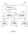
- FIG. 13is a block diagram depicting a system 100 in which the analog DLL 48 of FIG. 3 may be used.
- the system 100may include a data processing unit or computing unit 102 that includes a processor 104 for performing various computing functions, such as executing specific software to perform specific calculations or data processing tasks.
- the computing unit 102may also include memory devices 106 that are in communication with the processor 104 through a bus 108 .
- the bus 108may include an address bus (not shown), a data bus (not shown), and a control bus (not shown).
- Each of the memory device 106can be a dynamic random access memory (DRAM) chip or another type of memory circuits such as SRAM (Static Random Access Memory) chip or Flash memory.
- DRAMdynamic random access memory
- the DRAMcould be a synchronous DRAM commonly referred to as SGRAM (Synchronous Graphics Random Access Memory), SDRAM (Synchronous Dynamic Random Access Memory), SDRAM II, or DDR SDRAM (Double Data Rate SDRAM), as well as Synchlink or Rambus DRAMs.
- SGRAMSynchronous Graphics Random Access Memory
- SDRAMSerial Dynamic Random Access Memory
- SDRAM IISerial Dynamic Random Access Memory
- DDR SDRAMDouble Data Rate SDRAM
- Synchlink or Rambus DRAMsSynchlink or Rambus DRAMs.
- the processor 104can perform a plurality of functions based on information and data stored in the memory devices 106 .
- the processor 104can be a microprocessor, digital signal processor, embedded processor, micro-controller, dedicated memory test chip, or the like.
- Each of the memory devices 106may have construction similar to that shown in FIG. 1 , with the exception that the DLL unit 28 of the prior art is replaced by the analog DLL 48 ( FIG. 3 ) according to one embodiment of the present disclosure.
- a memory controller 110controls data communication to and from the memory devices 106 in response to control signals (not shown) received from the processor 104 over the bus 112 .
- the memory controller 110may include a command decode circuit (not shown).
- the command decode circuitmay receive the input control signals (on the bus 112 ) (not shown) to determine the modes of operation of one or more of the memory devices 106 .
- Some examples of the input signals or control signals (not shown in FIG. 13 ) on the bus 112 (and also on the bus 108 )include an External Clock signal, a Chip Select signal, a Row Access Strobe signal, a Column Access Strobe signal, a Write Enable signal, etc.
- the system 100may include one or more input devices 114 (e.g., a keyboard, a mouse, etc.) connected to the computing unit 102 to allow a user to manually input data, instructions, etc., to operate the computing unit 102 .
- One or more output devices 116 connected to the computing unit 102may also be provided as part of the system 100 to display or otherwise output data generated by the processor 104 . Examples of output devices 116 include printers, video terminals or video display units (VDUs).
- the system 100also includes one or more data storage devices 118 connected to the data processing unit 102 to allow the processor 104 to store data in or retrieve data from internal or external storage media (not shown). Examples of typical data storage devices 118 include drives that accept hard and floppy disks, CD-ROMs (compact disk read-only memories), and tape cassettes.
- the analog DLL 48may receive reference clock frequencies in the range of 800 MHz–1 GHz. In that case, a small clock jitter may distort the duty cycle. Therefore, it may be preferable to utilize a reference clock frequency with 50% duty cycle. Furthermore, it is observed that the DLL 48 may be designed to be free from stability considerations, unless the feedback delay is extremely large.
- the foregoingdescribes a methodology to devise an analog delay locked loop (DLL) or phase locked loop (PLL) wherein the delay stages may be programmed according to the operating condition, which may depend on the frequency of the input reference clock.
- DLLdelay locked loop
- PLLphase locked loop
- the resulting optimized delay stagesallow for broad frequency range of operation, fast locking time over a wide range of input clock frequencies, and a lower current consumption at high clock frequencies.
- Better performanceis achieved by allowing the number of analog delay stages active during a given operation to be flexibly set.
- the deactivation or turning off of unused delay stagesconserves power at higher frequencies.
- the high frequency range of operationis increased because of the removal of the prior art restriction of using a fixed number of delay stages for all input clock frequencies.
Landscapes
- Stabilization Of Oscillater, Synchronisation, Frequency Synthesizers (AREA)
- Dram (AREA)
Abstract
Description
Claims (20)
Priority Applications (5)
| Application Number | Priority Date | Filing Date | Title |
|---|---|---|---|
| US10/893,804US7149145B2 (en) | 2004-07-19 | 2004-07-19 | Delay stage-interweaved analog DLL/PLL |
| US11/297,184US7489568B2 (en) | 2004-07-19 | 2005-12-08 | Delay stage-interweaved analog DLL/PLL |
| US11/297,181US7447106B2 (en) | 2004-07-19 | 2005-12-08 | Delay stage-interweaved analog DLL/PLL |
| US11/297,768US7382678B2 (en) | 2004-07-19 | 2005-12-08 | Delay stage-interweaved analog DLL/PLL |
| US12/252,618US7835205B2 (en) | 2004-07-19 | 2008-10-16 | Delay stage-interweaved analog DLL/PLL |
Applications Claiming Priority (1)
| Application Number | Priority Date | Filing Date | Title |
|---|---|---|---|
| US10/893,804US7149145B2 (en) | 2004-07-19 | 2004-07-19 | Delay stage-interweaved analog DLL/PLL |
Related Child Applications (3)
| Application Number | Title | Priority Date | Filing Date |
|---|---|---|---|
| US11/297,184DivisionUS7489568B2 (en) | 2004-07-19 | 2005-12-08 | Delay stage-interweaved analog DLL/PLL |
| US11/297,768DivisionUS7382678B2 (en) | 2004-07-19 | 2005-12-08 | Delay stage-interweaved analog DLL/PLL |
| US11/297,181DivisionUS7447106B2 (en) | 2004-07-19 | 2005-12-08 | Delay stage-interweaved analog DLL/PLL |
Publications (2)
| Publication Number | Publication Date |
|---|---|
| US20060023562A1 US20060023562A1 (en) | 2006-02-02 |
| US7149145B2true US7149145B2 (en) | 2006-12-12 |
Family
ID=35732017
Family Applications (5)
| Application Number | Title | Priority Date | Filing Date |
|---|---|---|---|
| US10/893,804Expired - LifetimeUS7149145B2 (en) | 2004-07-19 | 2004-07-19 | Delay stage-interweaved analog DLL/PLL |
| US11/297,181Expired - LifetimeUS7447106B2 (en) | 2004-07-19 | 2005-12-08 | Delay stage-interweaved analog DLL/PLL |
| US11/297,768Expired - LifetimeUS7382678B2 (en) | 2004-07-19 | 2005-12-08 | Delay stage-interweaved analog DLL/PLL |
| US11/297,184Expired - LifetimeUS7489568B2 (en) | 2004-07-19 | 2005-12-08 | Delay stage-interweaved analog DLL/PLL |
| US12/252,618Expired - LifetimeUS7835205B2 (en) | 2004-07-19 | 2008-10-16 | Delay stage-interweaved analog DLL/PLL |
Family Applications After (4)
| Application Number | Title | Priority Date | Filing Date |
|---|---|---|---|
| US11/297,181Expired - LifetimeUS7447106B2 (en) | 2004-07-19 | 2005-12-08 | Delay stage-interweaved analog DLL/PLL |
| US11/297,768Expired - LifetimeUS7382678B2 (en) | 2004-07-19 | 2005-12-08 | Delay stage-interweaved analog DLL/PLL |
| US11/297,184Expired - LifetimeUS7489568B2 (en) | 2004-07-19 | 2005-12-08 | Delay stage-interweaved analog DLL/PLL |
| US12/252,618Expired - LifetimeUS7835205B2 (en) | 2004-07-19 | 2008-10-16 | Delay stage-interweaved analog DLL/PLL |
Country Status (1)
| Country | Link |
|---|---|
| US (5) | US7149145B2 (en) |
Cited By (41)
| Publication number | Priority date | Publication date | Assignee | Title |
|---|---|---|---|---|
| US20060039205A1 (en)* | 2004-08-23 | 2006-02-23 | Cornelius William P | Reducing the number of power and ground pins required to drive address signals to memory modules |
| US20060087435A1 (en)* | 2004-07-19 | 2006-04-27 | Micron Technology, Inc. | Delay stage-interweaved analog DLL/PLL |
| US20060273827A1 (en)* | 2005-06-02 | 2006-12-07 | Samsung Electronics Co., Ltd. | Systems, apparatuses and methods for synchronizing clock signals |
| US20090167386A1 (en)* | 2007-12-27 | 2009-07-02 | Taek-Sang Song | Charge pumping circuit, clock synchronization circuit having the charge pumping circuit, and method for operating the clock synchronization circuit |
| US7580312B2 (en) | 2006-07-31 | 2009-08-25 | Metaram, Inc. | Power saving system and method for use with a plurality of memory circuits |
| US7581127B2 (en) | 2006-07-31 | 2009-08-25 | Metaram, Inc. | Interface circuit system and method for performing power saving operations during a command-related latency |
| US7599205B2 (en) | 2005-09-02 | 2009-10-06 | Metaram, Inc. | Methods and apparatus of stacking DRAMs |
| US7609567B2 (en) | 2005-06-24 | 2009-10-27 | Metaram, Inc. | System and method for simulating an aspect of a memory circuit |
| US7724589B2 (en)* | 2006-07-31 | 2010-05-25 | Google Inc. | System and method for delaying a signal communicated from a system to at least one of a plurality of memory circuits |
| US7730338B2 (en) | 2006-07-31 | 2010-06-01 | Google Inc. | Interface circuit system and method for autonomously performing power management operations in conjunction with a plurality of memory circuits |
| US7761724B2 (en) | 2006-07-31 | 2010-07-20 | Google Inc. | Interface circuit system and method for performing power management operations in conjunction with only a portion of a memory circuit |
| US8019589B2 (en) | 2006-07-31 | 2011-09-13 | Google Inc. | Memory apparatus operable to perform a power-saving operation |
| US8055833B2 (en) | 2006-10-05 | 2011-11-08 | Google Inc. | System and method for increasing capacity, performance, and flexibility of flash storage |
| US8060774B2 (en) | 2005-06-24 | 2011-11-15 | Google Inc. | Memory systems and memory modules |
| US8077535B2 (en) | 2006-07-31 | 2011-12-13 | Google Inc. | Memory refresh apparatus and method |
| US8080874B1 (en) | 2007-09-14 | 2011-12-20 | Google Inc. | Providing additional space between an integrated circuit and a circuit board for positioning a component therebetween |
| US8081474B1 (en) | 2007-12-18 | 2011-12-20 | Google Inc. | Embossed heat spreader |
| US8090897B2 (en) | 2006-07-31 | 2012-01-03 | Google Inc. | System and method for simulating an aspect of a memory circuit |
| US8089795B2 (en) | 2006-02-09 | 2012-01-03 | Google Inc. | Memory module with memory stack and interface with enhanced capabilities |
| US8111566B1 (en) | 2007-11-16 | 2012-02-07 | Google, Inc. | Optimal channel design for memory devices for providing a high-speed memory interface |
| US8130560B1 (en) | 2006-11-13 | 2012-03-06 | Google Inc. | Multi-rank partial width memory modules |
| US8169233B2 (en) | 2009-06-09 | 2012-05-01 | Google Inc. | Programming of DIMM termination resistance values |
| US8209479B2 (en) | 2007-07-18 | 2012-06-26 | Google Inc. | Memory circuit system and method |
| US8244971B2 (en) | 2006-07-31 | 2012-08-14 | Google Inc. | Memory circuit system and method |
| US8280714B2 (en) | 2006-07-31 | 2012-10-02 | Google Inc. | Memory circuit simulation system and method with refresh capabilities |
| US8327104B2 (en) | 2006-07-31 | 2012-12-04 | Google Inc. | Adjusting the timing of signals associated with a memory system |
| US8335894B1 (en) | 2008-07-25 | 2012-12-18 | Google Inc. | Configurable memory system with interface circuit |
| US8386722B1 (en) | 2008-06-23 | 2013-02-26 | Google Inc. | Stacked DIMM memory interface |
| US8397013B1 (en) | 2006-10-05 | 2013-03-12 | Google Inc. | Hybrid memory module |
| US8438328B2 (en) | 2008-02-21 | 2013-05-07 | Google Inc. | Emulation of abstracted DIMMs using abstracted DRAMs |
| US8566516B2 (en) | 2006-07-31 | 2013-10-22 | Google Inc. | Refresh management of memory modules |
| US8796830B1 (en) | 2006-09-01 | 2014-08-05 | Google Inc. | Stackable low-profile lead frame package |
| US8972673B2 (en) | 2006-07-31 | 2015-03-03 | Google Inc. | Power management of memory circuits by virtual memory simulation |
| US20150256187A1 (en)* | 2014-03-04 | 2015-09-10 | Samsung Electronics Co., Ltd. | Delay locked loop, method of operating the same, and memory system including the same |
| US9171585B2 (en) | 2005-06-24 | 2015-10-27 | Google Inc. | Configurable memory circuit system and method |
| US9507739B2 (en) | 2005-06-24 | 2016-11-29 | Google Inc. | Configurable memory circuit system and method |
| US9542353B2 (en) | 2006-02-09 | 2017-01-10 | Google Inc. | System and method for reducing command scheduling constraints of memory circuits |
| US9632929B2 (en) | 2006-02-09 | 2017-04-25 | Google Inc. | Translating an address associated with a command communicated between a system and memory circuits |
| US10013371B2 (en) | 2005-06-24 | 2018-07-03 | Google Llc | Configurable memory circuit system and method |
| WO2020251709A1 (en)* | 2019-06-13 | 2020-12-17 | Intel Corporation | Apparatus and method to maintain stable clocking |
| US20230308103A1 (en)* | 2019-09-06 | 2023-09-28 | SK Hynix Inc. | Delay line, a delay locked loop circuit and a semiconductor apparatus using the delay line and the delay locked loop circuit |
Families Citing this family (16)
| Publication number | Priority date | Publication date | Assignee | Title |
|---|---|---|---|---|
| US8164368B2 (en)* | 2005-04-19 | 2012-04-24 | Micron Technology, Inc. | Power savings mode for memory systems |
| KR100809692B1 (en)* | 2006-08-01 | 2008-03-06 | 삼성전자주식회사 | Delay locked loop circuit having low jitter and jitter reducing method thereof |
| KR100846386B1 (en)* | 2006-09-21 | 2008-07-15 | 주식회사 하이닉스반도체 | Multi port memory device |
| US8064666B2 (en)* | 2007-04-10 | 2011-11-22 | Avantis Medical Systems, Inc. | Method and device for examining or imaging an interior surface of a cavity |
| KR100884590B1 (en)* | 2007-11-02 | 2009-02-19 | 주식회사 하이닉스반도체 | Delay locked circuit, semiconductor device, semiconductor memory device and operation method thereof |
| KR20090045773A (en)* | 2007-11-02 | 2009-05-08 | 주식회사 하이닉스반도체 | Delayed fixed circuit of semiconductor device operating at high speed |
| US7755404B2 (en)* | 2008-02-05 | 2010-07-13 | Micron Technology, Inc. | Delay locked loop circuit and method |
| US8032778B2 (en)* | 2008-03-19 | 2011-10-04 | Micron Technology, Inc. | Clock distribution apparatus, systems, and methods |
| KR101027676B1 (en)* | 2008-06-26 | 2011-04-12 | 주식회사 하이닉스반도체 | Phase synchronizer |
| JP5458556B2 (en)* | 2008-11-27 | 2014-04-02 | ソニー株式会社 | Timing adjustment circuit, solid-state imaging device, and camera system |
| JP2010200090A (en)* | 2009-02-26 | 2010-09-09 | Toshiba Corp | Phase compensation clock synchronizing circuit |
| US9191193B1 (en) | 2014-07-18 | 2015-11-17 | Qualcomm Incorporated | Clock synchronization |
| DE102015200690A1 (en)* | 2015-01-19 | 2016-07-21 | Siemens Aktiengesellschaft | Proazaphosphatrans as n-dopants in organic electronics |
| KR102656696B1 (en)* | 2016-12-06 | 2024-04-12 | 에스케이하이닉스 주식회사 | Semiconductor device |
| US10263627B1 (en)* | 2017-12-12 | 2019-04-16 | Nxp Usa, Inc. | Delay-locked loop having initialization circuit |
| US11206026B2 (en) | 2019-09-06 | 2021-12-21 | SK Hynix Inc. | Delay line, a delay locked loop circuit and a semiconductor apparatus using the delay line and the delay locked loop circuit |
Citations (14)
| Publication number | Priority date | Publication date | Assignee | Title |
|---|---|---|---|---|
| US5799051A (en)* | 1992-05-28 | 1998-08-25 | Rambus, Inc. | Delay stage circuitry for a ring oscillator |
| US6011732A (en)* | 1997-08-20 | 2000-01-04 | Micron Technology, Inc. | Synchronous clock generator including a compound delay-locked loop |
| US6125364A (en)* | 1997-11-06 | 2000-09-26 | International Business Machines Corporation | Flexible object persistence framework using data cursor objects loaded from superclasses |
| US6208183B1 (en)* | 1999-04-30 | 2001-03-27 | Conexant Systems, Inc. | Gated delay-locked loop for clock generation applications |
| JP2001285266A (en)* | 2000-03-30 | 2001-10-12 | Nec Corp | Digital phase control circuit |
| US6346839B1 (en)* | 2000-04-03 | 2002-02-12 | Mosel Vitelic Inc. | Low power consumption integrated circuit delay locked loop and method for controlling the same |
| US6445231B1 (en)* | 2000-06-01 | 2002-09-03 | Micron Technology, Inc. | Digital dual-loop DLL design using coarse and fine loops |
| US6621314B2 (en)* | 2001-09-25 | 2003-09-16 | Intel Corporation | Delay locked loop |
| USRE38482E1 (en)* | 1992-05-28 | 2004-03-30 | Rambus Inc. | Delay stage circuitry for a ring oscillator |
| US20040125905A1 (en)* | 2002-12-31 | 2004-07-01 | Mosaid Technologies, Inc. | Wide frequency range delay locked loop |
| US6779126B1 (en)* | 2000-08-31 | 2004-08-17 | Micron Technology, Inc. | Phase detector for all-digital phase locked and delay locked loops |
| US20050050375A1 (en)* | 2003-08-29 | 2005-03-03 | Mark Novak | Memory interface system and method |
| US6867627B1 (en)* | 2003-09-16 | 2005-03-15 | Integrated Device Technology, Inc. | Delay-locked loop (DLL) integrated circuits having high bandwidth and reliable locking characteristics |
| US6914852B2 (en)* | 2003-03-12 | 2005-07-05 | Micron Technology, Inc. | Multi-frequency synchronizing clock signal generator |
Family Cites Families (55)
| Publication number | Priority date | Publication date | Assignee | Title |
|---|---|---|---|---|
| US5184027A (en)* | 1987-03-20 | 1993-02-02 | Hitachi, Ltd. | Clock signal supply system |
| US4868522A (en)* | 1988-12-13 | 1989-09-19 | Gazelle Microcircuits, Inc. | Clock signal distribution device |
| US4994695A (en)* | 1989-11-13 | 1991-02-19 | Intel Corporation | Synchronous delay line with quadrature clock phases |
| US5036230A (en)* | 1990-03-01 | 1991-07-30 | Intel Corporation | CMOS clock-phase synthesizer |
| DE4211701A1 (en)* | 1992-04-08 | 1993-10-14 | Thomson Brandt Gmbh | Method and device for phase measurement |
| US5317202A (en)* | 1992-05-28 | 1994-05-31 | Intel Corporation | Delay line loop for 1X on-chip clock generation with zero skew and 50% duty cycle |
| DE69535087T2 (en)* | 1994-03-11 | 2006-12-21 | Fujitsu Ltd., Kawasaki | Circuit arrangement for clock recovery |
| US5714904A (en)* | 1994-06-06 | 1998-02-03 | Sun Microsystems, Inc. | High speed serial link for fully duplexed data communication |
| US5515403A (en)* | 1994-06-21 | 1996-05-07 | Dsc Communications Corporation | Apparatus and method for clock alignment and switching |
| US5684421A (en)* | 1995-10-13 | 1997-11-04 | Credence Systems Corporation | Compensated delay locked loop timing vernier |
| US5642082A (en)* | 1996-06-20 | 1997-06-24 | Altera Corporation | Loop filter level detection circuit and method |
| JP3487532B2 (en)* | 1996-07-08 | 2004-01-19 | 株式会社東芝 | Data processing device, semiconductor storage device, and data processing method |
| US6104225A (en)* | 1997-04-21 | 2000-08-15 | Fujitsu Limited | Semiconductor device using complementary clock and signal input state detection circuit used for the same |
| CA2204089C (en)* | 1997-04-30 | 2001-08-07 | Mosaid Technologies Incorporated | Digital delay locked loop |
| JP3309782B2 (en)* | 1997-06-10 | 2002-07-29 | 日本電気株式会社 | Semiconductor integrated circuit |
| US6247138B1 (en)* | 1997-06-12 | 2001-06-12 | Fujitsu Limited | Timing signal generating circuit, semiconductor integrated circuit device and semiconductor integrated circuit system to which the timing signal generating circuit is applied, and signal transmission system |
| JP3209943B2 (en)* | 1997-06-13 | 2001-09-17 | 沖電気工業株式会社 | Voltage control delay circuit, direct phase control type voltage controlled oscillator, clock / data recovery circuit, and clock / data recovery device |
| US5999576A (en)* | 1997-07-14 | 1999-12-07 | Realtek Semiconductor Corp. | Delay-locked loop for data recovery |
| US6073259A (en)* | 1997-08-05 | 2000-06-06 | Teradyne, Inc. | Low cost CMOS tester with high channel density |
| US6088255A (en)* | 1998-03-20 | 2000-07-11 | Fujitsu Limited | Semiconductor device with prompt timing stabilization |
| JP3439670B2 (en)* | 1998-10-15 | 2003-08-25 | 富士通株式会社 | Timing clock generation circuit using hierarchical DLL circuit |
| KR100301048B1 (en)* | 1998-10-19 | 2001-09-06 | 윤종용 | Delay lock loop having variable stage and operating method |
| US6369624B1 (en)* | 1998-11-03 | 2002-04-09 | Altera Corporation | Programmable phase shift circuitry |
| JP2000163961A (en)* | 1998-11-26 | 2000-06-16 | Mitsubishi Electric Corp | Synchronous semiconductor integrated circuit device |
| JP3973308B2 (en)* | 1998-11-27 | 2007-09-12 | 富士通株式会社 | Integrated circuit device incorporating a self-timing control circuit |
| US6157694A (en)* | 1998-12-09 | 2000-12-05 | Lucent Technologies, Inc. | Fractional frequency divider |
| US6310498B1 (en)* | 1998-12-09 | 2001-10-30 | Agere Systems Guardian Corp. | Digital phase selection circuitry and method for reducing jitter |
| US6483886B1 (en)* | 1999-01-08 | 2002-11-19 | Altera Corporation | Phase-locked loop circuitry for programmable logic devices |
| KR100319890B1 (en)* | 1999-01-26 | 2002-01-10 | 윤종용 | Delay locked loop and method for controlling the same |
| KR100331562B1 (en)* | 1999-11-29 | 2002-04-06 | 윤종용 | Delay locked loop circuit and method for generating internal clock signal |
| US6317381B1 (en)* | 1999-12-07 | 2001-11-13 | Micron Technology, Inc. | Method and system for adaptively adjusting control signal timing in a memory device |
| KR100331566B1 (en)* | 2000-01-22 | 2002-04-06 | 윤종용 | Clock synchronization circuit and semiconductor device having the clock synchronization circuit |
| JP3984412B2 (en)* | 2000-05-26 | 2007-10-03 | 富士通株式会社 | Variable delay circuit and semiconductor integrated circuit having variable delay circuit |
| US6525615B1 (en)* | 2000-07-14 | 2003-02-25 | International Business Machines Corporation | Oscillator with digitally variable phase for a phase-locked loop |
| JP3807593B2 (en)* | 2000-07-24 | 2006-08-09 | 株式会社ルネサステクノロジ | Clock generation circuit, control method, and semiconductor memory device |
| KR100385232B1 (en)* | 2000-08-07 | 2003-05-27 | 삼성전자주식회사 | Synchronizer between two different clock frequencies |
| US6868504B1 (en)* | 2000-08-31 | 2005-03-15 | Micron Technology, Inc. | Interleaved delay line for phase locked and delay locked loops |
| US6768356B1 (en)* | 2000-09-07 | 2004-07-27 | Iowa State University Research Foundation, Inc. | Apparatus for and method of implementing time-interleaved architecture |
| JP4407031B2 (en)* | 2000-09-21 | 2010-02-03 | ソニー株式会社 | Phase-locked loop circuit and delay-locked loop circuit |
| JP4526194B2 (en)* | 2001-01-11 | 2010-08-18 | ルネサスエレクトロニクス株式会社 | Oversampling clock recovery method and circuit |
| US6771103B2 (en)* | 2001-03-14 | 2004-08-03 | Denso Corporation | Time measurement apparatus, distance measurement apparatus, and clock signal generating apparatus usable therein |
| JP2002353809A (en)* | 2001-05-28 | 2002-12-06 | Mitsubishi Electric Corp | Clock generation circuit |
| KR100423012B1 (en)* | 2001-09-28 | 2004-03-16 | 주식회사 버카나와이어리스코리아 | DLL with False Lock Protector |
| US6426662B1 (en)* | 2001-11-12 | 2002-07-30 | Pericom Semiconductor Corp. | Twisted-ring oscillator and delay line generating multiple phases using differential dividers and comparators to match delays |
| US6794912B2 (en)* | 2002-02-18 | 2004-09-21 | Matsushita Electric Industrial Co., Ltd. | Multi-phase clock transmission circuit and method |
| JP3966012B2 (en)* | 2002-02-21 | 2007-08-29 | セイコーエプソン株式会社 | Multiphase clock generation circuit and clock multiplication circuit |
| JP4031671B2 (en)* | 2002-06-11 | 2008-01-09 | 松下電器産業株式会社 | Clock recovery circuit |
| KR100531469B1 (en)* | 2003-01-09 | 2005-11-28 | 주식회사 하이닉스반도체 | Analog Delay Lock Loop with store circuit about delay lock |
| US6937076B2 (en)* | 2003-06-11 | 2005-08-30 | Micron Technology, Inc. | Clock synchronizing apparatus and method using frequency dependent variable delay |
| US7098714B2 (en)* | 2003-12-08 | 2006-08-29 | Micron Technology, Inc. | Centralizing the lock point of a synchronous circuit |
| US6982579B2 (en)* | 2003-12-11 | 2006-01-03 | Micron Technology, Inc. | Digital frequency-multiplying DLLs |
| US7149145B2 (en)* | 2004-07-19 | 2006-12-12 | Micron Technology, Inc. | Delay stage-interweaved analog DLL/PLL |
| US7138845B2 (en)* | 2004-07-22 | 2006-11-21 | Micron Technology, Inc. | Method and apparatus to set a tuning range for an analog delay |
| US7282972B2 (en)* | 2005-07-29 | 2007-10-16 | Micron Technology, Inc. | Bias generator with feedback control |
| US7271634B1 (en)* | 2005-09-16 | 2007-09-18 | Advanced Micro Devices, Inc. | Delay-locked loop having a plurality of lock modes |
- 2004
- 2004-07-19USUS10/893,804patent/US7149145B2/ennot_activeExpired - Lifetime
- 2005
- 2005-12-08USUS11/297,181patent/US7447106B2/ennot_activeExpired - Lifetime
- 2005-12-08USUS11/297,768patent/US7382678B2/ennot_activeExpired - Lifetime
- 2005-12-08USUS11/297,184patent/US7489568B2/ennot_activeExpired - Lifetime
- 2008
- 2008-10-16USUS12/252,618patent/US7835205B2/ennot_activeExpired - Lifetime
Patent Citations (16)
| Publication number | Priority date | Publication date | Assignee | Title |
|---|---|---|---|---|
| US5799051A (en)* | 1992-05-28 | 1998-08-25 | Rambus, Inc. | Delay stage circuitry for a ring oscillator |
| USRE38482E1 (en)* | 1992-05-28 | 2004-03-30 | Rambus Inc. | Delay stage circuitry for a ring oscillator |
| US6011732A (en)* | 1997-08-20 | 2000-01-04 | Micron Technology, Inc. | Synchronous clock generator including a compound delay-locked loop |
| US6125364A (en)* | 1997-11-06 | 2000-09-26 | International Business Machines Corporation | Flexible object persistence framework using data cursor objects loaded from superclasses |
| US6208183B1 (en)* | 1999-04-30 | 2001-03-27 | Conexant Systems, Inc. | Gated delay-locked loop for clock generation applications |
| JP2001285266A (en)* | 2000-03-30 | 2001-10-12 | Nec Corp | Digital phase control circuit |
| US6346839B1 (en)* | 2000-04-03 | 2002-02-12 | Mosel Vitelic Inc. | Low power consumption integrated circuit delay locked loop and method for controlling the same |
| US6774690B2 (en)* | 2000-06-01 | 2004-08-10 | Micron Technology, Inc. | Digital dual-loop DLL design using coarse and fine loops |
| US6445231B1 (en)* | 2000-06-01 | 2002-09-03 | Micron Technology, Inc. | Digital dual-loop DLL design using coarse and fine loops |
| US20020180501A1 (en)* | 2000-06-01 | 2002-12-05 | Micron Technology, Inc. | Digital dual-loop DLL design using coarse and fine loops |
| US6779126B1 (en)* | 2000-08-31 | 2004-08-17 | Micron Technology, Inc. | Phase detector for all-digital phase locked and delay locked loops |
| US6621314B2 (en)* | 2001-09-25 | 2003-09-16 | Intel Corporation | Delay locked loop |
| US20040125905A1 (en)* | 2002-12-31 | 2004-07-01 | Mosaid Technologies, Inc. | Wide frequency range delay locked loop |
| US6914852B2 (en)* | 2003-03-12 | 2005-07-05 | Micron Technology, Inc. | Multi-frequency synchronizing clock signal generator |
| US20050050375A1 (en)* | 2003-08-29 | 2005-03-03 | Mark Novak | Memory interface system and method |
| US6867627B1 (en)* | 2003-09-16 | 2005-03-15 | Integrated Device Technology, Inc. | Delay-locked loop (DLL) integrated circuits having high bandwidth and reliable locking characteristics |
Non-Patent Citations (1)
| Title |
|---|
| John G. Maneatis, Low-Jitter Process-Independent DLL and PLL Based on Self-Biased Techniques, IEEE Journal, Nov. 1996, 1723-1732, vol. 31, No. 11. |
Cited By (83)
| Publication number | Priority date | Publication date | Assignee | Title |
|---|---|---|---|---|
| US20060087435A1 (en)* | 2004-07-19 | 2006-04-27 | Micron Technology, Inc. | Delay stage-interweaved analog DLL/PLL |
| US20060087907A1 (en)* | 2004-07-19 | 2006-04-27 | Micron Technology, Inc. | Delay stage-interweaved analog DLL/PLL |
| US7447106B2 (en)* | 2004-07-19 | 2008-11-04 | Micron Technology, Inc. | Delay stage-interweaved analog DLL/PLL |
| US7489568B2 (en)* | 2004-07-19 | 2009-02-10 | Micron Technology, Inc. | Delay stage-interweaved analog DLL/PLL |
| US20090066379A1 (en)* | 2004-07-19 | 2009-03-12 | Micron Technology, Inc. | Delay Stage-Interweaved Analog DLL/PLL |
| US7835205B2 (en)* | 2004-07-19 | 2010-11-16 | Micron Technology, Inc. | Delay stage-interweaved analog DLL/PLL |
| US20060039205A1 (en)* | 2004-08-23 | 2006-02-23 | Cornelius William P | Reducing the number of power and ground pins required to drive address signals to memory modules |
| US7586348B2 (en)* | 2005-06-02 | 2009-09-08 | Samsung Electronics Co., Ltd. | Systems, apparatuses and methods for synchronizing clock signals |
| US20060273827A1 (en)* | 2005-06-02 | 2006-12-07 | Samsung Electronics Co., Ltd. | Systems, apparatuses and methods for synchronizing clock signals |
| US8615679B2 (en) | 2005-06-24 | 2013-12-24 | Google Inc. | Memory modules with reliability and serviceability functions |
| US8386833B2 (en) | 2005-06-24 | 2013-02-26 | Google Inc. | Memory systems and memory modules |
| US10013371B2 (en) | 2005-06-24 | 2018-07-03 | Google Llc | Configurable memory circuit system and method |
| US8359187B2 (en) | 2005-06-24 | 2013-01-22 | Google Inc. | Simulating a different number of memory circuit devices |
| US7609567B2 (en) | 2005-06-24 | 2009-10-27 | Metaram, Inc. | System and method for simulating an aspect of a memory circuit |
| US9171585B2 (en) | 2005-06-24 | 2015-10-27 | Google Inc. | Configurable memory circuit system and method |
| US9507739B2 (en) | 2005-06-24 | 2016-11-29 | Google Inc. | Configurable memory circuit system and method |
| US8060774B2 (en) | 2005-06-24 | 2011-11-15 | Google Inc. | Memory systems and memory modules |
| US7599205B2 (en) | 2005-09-02 | 2009-10-06 | Metaram, Inc. | Methods and apparatus of stacking DRAMs |
| US8619452B2 (en) | 2005-09-02 | 2013-12-31 | Google Inc. | Methods and apparatus of stacking DRAMs |
| US8582339B2 (en) | 2005-09-02 | 2013-11-12 | Google Inc. | System including memory stacks |
| US8811065B2 (en) | 2005-09-02 | 2014-08-19 | Google Inc. | Performing error detection on DRAMs |
| US9542353B2 (en) | 2006-02-09 | 2017-01-10 | Google Inc. | System and method for reducing command scheduling constraints of memory circuits |
| US9727458B2 (en) | 2006-02-09 | 2017-08-08 | Google Inc. | Translating an address associated with a command communicated between a system and memory circuits |
| US8566556B2 (en) | 2006-02-09 | 2013-10-22 | Google Inc. | Memory module with memory stack and interface with enhanced capabilities |
| US9632929B2 (en) | 2006-02-09 | 2017-04-25 | Google Inc. | Translating an address associated with a command communicated between a system and memory circuits |
| US9542352B2 (en) | 2006-02-09 | 2017-01-10 | Google Inc. | System and method for reducing command scheduling constraints of memory circuits |
| US8797779B2 (en) | 2006-02-09 | 2014-08-05 | Google Inc. | Memory module with memory stack and interface with enhanced capabilites |
| US8089795B2 (en) | 2006-02-09 | 2012-01-03 | Google Inc. | Memory module with memory stack and interface with enhanced capabilities |
| US8972673B2 (en) | 2006-07-31 | 2015-03-03 | Google Inc. | Power management of memory circuits by virtual memory simulation |
| US7581127B2 (en) | 2006-07-31 | 2009-08-25 | Metaram, Inc. | Interface circuit system and method for performing power saving operations during a command-related latency |
| US8154935B2 (en) | 2006-07-31 | 2012-04-10 | Google Inc. | Delaying a signal communicated from a system to at least one of a plurality of memory circuits |
| US7724589B2 (en)* | 2006-07-31 | 2010-05-25 | Google Inc. | System and method for delaying a signal communicated from a system to at least one of a plurality of memory circuits |
| US9047976B2 (en) | 2006-07-31 | 2015-06-02 | Google Inc. | Combined signal delay and power saving for use with a plurality of memory circuits |
| US8244971B2 (en) | 2006-07-31 | 2012-08-14 | Google Inc. | Memory circuit system and method |
| US8280714B2 (en) | 2006-07-31 | 2012-10-02 | Google Inc. | Memory circuit simulation system and method with refresh capabilities |
| US8327104B2 (en) | 2006-07-31 | 2012-12-04 | Google Inc. | Adjusting the timing of signals associated with a memory system |
| US8019589B2 (en) | 2006-07-31 | 2011-09-13 | Google Inc. | Memory apparatus operable to perform a power-saving operation |
| US8340953B2 (en) | 2006-07-31 | 2012-12-25 | Google, Inc. | Memory circuit simulation with power saving capabilities |
| US8671244B2 (en) | 2006-07-31 | 2014-03-11 | Google Inc. | Simulating a memory standard |
| US7590796B2 (en) | 2006-07-31 | 2009-09-15 | Metaram, Inc. | System and method for power management in memory systems |
| US8868829B2 (en) | 2006-07-31 | 2014-10-21 | Google Inc. | Memory circuit system and method |
| US7730338B2 (en) | 2006-07-31 | 2010-06-01 | Google Inc. | Interface circuit system and method for autonomously performing power management operations in conjunction with a plurality of memory circuits |
| US8112266B2 (en) | 2006-07-31 | 2012-02-07 | Google Inc. | Apparatus for simulating an aspect of a memory circuit |
| US8631220B2 (en) | 2006-07-31 | 2014-01-14 | Google Inc. | Adjusting the timing of signals associated with a memory system |
| US8090897B2 (en) | 2006-07-31 | 2012-01-03 | Google Inc. | System and method for simulating an aspect of a memory circuit |
| US8566516B2 (en) | 2006-07-31 | 2013-10-22 | Google Inc. | Refresh management of memory modules |
| US8077535B2 (en) | 2006-07-31 | 2011-12-13 | Google Inc. | Memory refresh apparatus and method |
| US7761724B2 (en) | 2006-07-31 | 2010-07-20 | Google Inc. | Interface circuit system and method for performing power management operations in conjunction with only a portion of a memory circuit |
| US8595419B2 (en) | 2006-07-31 | 2013-11-26 | Google Inc. | Memory apparatus operable to perform a power-saving operation |
| US8601204B2 (en) | 2006-07-31 | 2013-12-03 | Google Inc. | Simulating a refresh operation latency |
| US7580312B2 (en) | 2006-07-31 | 2009-08-25 | Metaram, Inc. | Power saving system and method for use with a plurality of memory circuits |
| US8041881B2 (en) | 2006-07-31 | 2011-10-18 | Google Inc. | Memory device with emulated characteristics |
| US8745321B2 (en) | 2006-07-31 | 2014-06-03 | Google Inc. | Simulating a memory standard |
| US8796830B1 (en) | 2006-09-01 | 2014-08-05 | Google Inc. | Stackable low-profile lead frame package |
| US8370566B2 (en) | 2006-10-05 | 2013-02-05 | Google Inc. | System and method for increasing capacity, performance, and flexibility of flash storage |
| US8055833B2 (en) | 2006-10-05 | 2011-11-08 | Google Inc. | System and method for increasing capacity, performance, and flexibility of flash storage |
| US8977806B1 (en) | 2006-10-05 | 2015-03-10 | Google Inc. | Hybrid memory module |
| US8751732B2 (en) | 2006-10-05 | 2014-06-10 | Google Inc. | System and method for increasing capacity, performance, and flexibility of flash storage |
| US8397013B1 (en) | 2006-10-05 | 2013-03-12 | Google Inc. | Hybrid memory module |
| US8446781B1 (en) | 2006-11-13 | 2013-05-21 | Google Inc. | Multi-rank partial width memory modules |
| US8130560B1 (en) | 2006-11-13 | 2012-03-06 | Google Inc. | Multi-rank partial width memory modules |
| US8760936B1 (en) | 2006-11-13 | 2014-06-24 | Google Inc. | Multi-rank partial width memory modules |
| US8209479B2 (en) | 2007-07-18 | 2012-06-26 | Google Inc. | Memory circuit system and method |
| US8080874B1 (en) | 2007-09-14 | 2011-12-20 | Google Inc. | Providing additional space between an integrated circuit and a circuit board for positioning a component therebetween |
| US8675429B1 (en) | 2007-11-16 | 2014-03-18 | Google Inc. | Optimal channel design for memory devices for providing a high-speed memory interface |
| US8111566B1 (en) | 2007-11-16 | 2012-02-07 | Google, Inc. | Optimal channel design for memory devices for providing a high-speed memory interface |
| US8705240B1 (en) | 2007-12-18 | 2014-04-22 | Google Inc. | Embossed heat spreader |
| US8081474B1 (en) | 2007-12-18 | 2011-12-20 | Google Inc. | Embossed heat spreader |
| US8730670B1 (en) | 2007-12-18 | 2014-05-20 | Google Inc. | Embossed heat spreader |
| US20090167386A1 (en)* | 2007-12-27 | 2009-07-02 | Taek-Sang Song | Charge pumping circuit, clock synchronization circuit having the charge pumping circuit, and method for operating the clock synchronization circuit |
| US8438328B2 (en) | 2008-02-21 | 2013-05-07 | Google Inc. | Emulation of abstracted DIMMs using abstracted DRAMs |
| US8631193B2 (en) | 2008-02-21 | 2014-01-14 | Google Inc. | Emulation of abstracted DIMMS using abstracted DRAMS |
| US8386722B1 (en) | 2008-06-23 | 2013-02-26 | Google Inc. | Stacked DIMM memory interface |
| US8762675B2 (en) | 2008-06-23 | 2014-06-24 | Google Inc. | Memory system for synchronous data transmission |
| US8819356B2 (en) | 2008-07-25 | 2014-08-26 | Google Inc. | Configurable multirank memory system with interface circuit |
| US8335894B1 (en) | 2008-07-25 | 2012-12-18 | Google Inc. | Configurable memory system with interface circuit |
| US8169233B2 (en) | 2009-06-09 | 2012-05-01 | Google Inc. | Programming of DIMM termination resistance values |
| US20150256187A1 (en)* | 2014-03-04 | 2015-09-10 | Samsung Electronics Co., Ltd. | Delay locked loop, method of operating the same, and memory system including the same |
| US9306583B2 (en)* | 2014-03-04 | 2016-04-05 | Samsung Electronics Co., Ltd. | Delay locked loop, method of operating the same, and memory system including the same |
| WO2020251709A1 (en)* | 2019-06-13 | 2020-12-17 | Intel Corporation | Apparatus and method to maintain stable clocking |
| US11256287B2 (en) | 2019-06-13 | 2022-02-22 | Intel Corporation | Apparatus and method to maintain stable clocking |
| US20230308103A1 (en)* | 2019-09-06 | 2023-09-28 | SK Hynix Inc. | Delay line, a delay locked loop circuit and a semiconductor apparatus using the delay line and the delay locked loop circuit |
| US11942955B2 (en)* | 2019-09-06 | 2024-03-26 | SK Hynix Inc. | Delay line, a delay locked loop circuit and a semiconductor apparatus using the delay line and the delay locked loop circuit |
Also Published As
| Publication number | Publication date |
|---|---|
| US20090066379A1 (en) | 2009-03-12 |
| US7489568B2 (en) | 2009-02-10 |
| US20060087908A1 (en) | 2006-04-27 |
| US7447106B2 (en) | 2008-11-04 |
| US7835205B2 (en) | 2010-11-16 |
| US7382678B2 (en) | 2008-06-03 |
| US20060023562A1 (en) | 2006-02-02 |
| US20060087907A1 (en) | 2006-04-27 |
| US20060087435A1 (en) | 2006-04-27 |
Similar Documents
| Publication | Publication Date | Title |
|---|---|---|
| US7149145B2 (en) | Delay stage-interweaved analog DLL/PLL | |
| US7259604B2 (en) | Initialization scheme for a reduced-frequency, fifty percent duty cycle corrector | |
| US7208989B2 (en) | Synchronous clock generator including duty cycle correction | |
| US7327173B2 (en) | Delay-locked loop having a pre-shift phase detector | |
| US6906566B2 (en) | Dual-phase delay-locked loop circuit and method | |
| US8878586B2 (en) | Seamless coarse and fine delay structure for high performance DLL | |
| US6836166B2 (en) | Method and system for delay control in synchronization circuits | |
| US7423456B2 (en) | Fast response time, low power phase detector circuits, devices and systems incorporating the same, and associated methods | |
| US6693472B2 (en) | Method and circuit for adjusting the timing of output data based on an operational mode of output drivers | |
| US6803826B2 (en) | Delay-locked loop circuit and method using a ring oscillator and counter-based delay | |
| US9041446B2 (en) | Power savings mode for memory systems | |
| US7449939B2 (en) | Bias generator with feedback control |
Legal Events
| Date | Code | Title | Description |
|---|---|---|---|
| AS | Assignment | Owner name:MICRON TECHNOLOGY, INC., IDAHO Free format text:ASSIGNMENT OF ASSIGNORS INTEREST;ASSIGNORS:KIM, KANG YONG;CHOI, DONG MYUNG;REEL/FRAME:015585/0935 Effective date:20040709 | |
| FEPP | Fee payment procedure | Free format text:PAYOR NUMBER ASSIGNED (ORIGINAL EVENT CODE: ASPN); ENTITY STATUS OF PATENT OWNER: LARGE ENTITY | |
| STCF | Information on status: patent grant | Free format text:PATENTED CASE | |
| CC | Certificate of correction | ||
| FPAY | Fee payment | Year of fee payment:4 | |
| FPAY | Fee payment | Year of fee payment:8 | |
| AS | Assignment | Owner name:U.S. BANK NATIONAL ASSOCIATION, AS COLLATERAL AGENT, CALIFORNIA Free format text:SECURITY INTEREST;ASSIGNOR:MICRON TECHNOLOGY, INC.;REEL/FRAME:038669/0001 Effective date:20160426 Owner name:U.S. BANK NATIONAL ASSOCIATION, AS COLLATERAL AGEN Free format text:SECURITY INTEREST;ASSIGNOR:MICRON TECHNOLOGY, INC.;REEL/FRAME:038669/0001 Effective date:20160426 | |
| AS | Assignment | Owner name:MORGAN STANLEY SENIOR FUNDING, INC., AS COLLATERAL AGENT, MARYLAND Free format text:PATENT SECURITY AGREEMENT;ASSIGNOR:MICRON TECHNOLOGY, INC.;REEL/FRAME:038954/0001 Effective date:20160426 Owner name:MORGAN STANLEY SENIOR FUNDING, INC., AS COLLATERAL Free format text:PATENT SECURITY AGREEMENT;ASSIGNOR:MICRON TECHNOLOGY, INC.;REEL/FRAME:038954/0001 Effective date:20160426 | |
| AS | Assignment | Owner name:U.S. BANK NATIONAL ASSOCIATION, AS COLLATERAL AGENT, CALIFORNIA Free format text:CORRECTIVE ASSIGNMENT TO CORRECT THE REPLACE ERRONEOUSLY FILED PATENT #7358718 WITH THE CORRECT PATENT #7358178 PREVIOUSLY RECORDED ON REEL 038669 FRAME 0001. ASSIGNOR(S) HEREBY CONFIRMS THE SECURITY INTEREST;ASSIGNOR:MICRON TECHNOLOGY, INC.;REEL/FRAME:043079/0001 Effective date:20160426 Owner name:U.S. BANK NATIONAL ASSOCIATION, AS COLLATERAL AGEN Free format text:CORRECTIVE ASSIGNMENT TO CORRECT THE REPLACE ERRONEOUSLY FILED PATENT #7358718 WITH THE CORRECT PATENT #7358178 PREVIOUSLY RECORDED ON REEL 038669 FRAME 0001. ASSIGNOR(S) HEREBY CONFIRMS THE SECURITY INTEREST;ASSIGNOR:MICRON TECHNOLOGY, INC.;REEL/FRAME:043079/0001 Effective date:20160426 | |
| MAFP | Maintenance fee payment | Free format text:PAYMENT OF MAINTENANCE FEE, 12TH YEAR, LARGE ENTITY (ORIGINAL EVENT CODE: M1553) Year of fee payment:12 | |
| AS | Assignment | Owner name:JPMORGAN CHASE BANK, N.A., AS COLLATERAL AGENT, ILLINOIS Free format text:SECURITY INTEREST;ASSIGNORS:MICRON TECHNOLOGY, INC.;MICRON SEMICONDUCTOR PRODUCTS, INC.;REEL/FRAME:047540/0001 Effective date:20180703 Owner name:JPMORGAN CHASE BANK, N.A., AS COLLATERAL AGENT, IL Free format text:SECURITY INTEREST;ASSIGNORS:MICRON TECHNOLOGY, INC.;MICRON SEMICONDUCTOR PRODUCTS, INC.;REEL/FRAME:047540/0001 Effective date:20180703 | |
| AS | Assignment | Owner name:MICRON TECHNOLOGY, INC., IDAHO Free format text:RELEASE BY SECURED PARTY;ASSIGNOR:U.S. BANK NATIONAL ASSOCIATION, AS COLLATERAL AGENT;REEL/FRAME:047243/0001 Effective date:20180629 | |
| AS | Assignment | Owner name:MICRON TECHNOLOGY, INC., IDAHO Free format text:RELEASE BY SECURED PARTY;ASSIGNOR:MORGAN STANLEY SENIOR FUNDING, INC., AS COLLATERAL AGENT;REEL/FRAME:050937/0001 Effective date:20190731 | |
| AS | Assignment | Owner name:MICRON SEMICONDUCTOR PRODUCTS, INC., IDAHO Free format text:RELEASE BY SECURED PARTY;ASSIGNOR:JPMORGAN CHASE BANK, N.A., AS COLLATERAL AGENT;REEL/FRAME:051028/0001 Effective date:20190731 Owner name:MICRON TECHNOLOGY, INC., IDAHO Free format text:RELEASE BY SECURED PARTY;ASSIGNOR:JPMORGAN CHASE BANK, N.A., AS COLLATERAL AGENT;REEL/FRAME:051028/0001 Effective date:20190731 |