US7147759B2 - High-power pulsed magnetron sputtering - Google Patents
High-power pulsed magnetron sputteringDownload PDFInfo
- Publication number
- US7147759B2 US7147759B2US10/065,277US6527702AUS7147759B2US 7147759 B2US7147759 B2US 7147759B2US 6527702 AUS6527702 AUS 6527702AUS 7147759 B2US7147759 B2US 7147759B2
- Authority
- US
- United States
- Prior art keywords
- ionized plasma
- weakly
- sputtering
- source
- pulse
- Prior art date
- Legal status (The legal status is an assumption and is not a legal conclusion. Google has not performed a legal analysis and makes no representation as to the accuracy of the status listed.)
- Expired - Fee Related
Links
- 238000001755magnetron sputter depositionMethods0.000titledescription51
- 230000005291magnetic effectEffects0.000claimsabstractdescription89
- 238000004544sputter depositionMethods0.000claimsabstractdescription57
- 238000005477sputtering targetMethods0.000claimsabstractdescription53
- 230000005684electric fieldEffects0.000claimsabstractdescription51
- 150000002500ionsChemical class0.000claimsabstractdescription35
- 230000004907fluxEffects0.000claimsabstract3
- 238000000034methodMethods0.000claimsdescription54
- 239000013077target materialSubstances0.000claimsdescription33
- 239000000758substrateSubstances0.000claimsdescription24
- 238000000752ionisation methodMethods0.000claimsdescription19
- 230000015556catabolic processEffects0.000claimsdescription14
- 239000000463materialSubstances0.000claimsdescription10
- 230000003628erosive effectEffects0.000claimsdescription7
- 230000005284excitationEffects0.000claimsdescription6
- 239000000696magnetic materialSubstances0.000claimsdescription4
- 238000010894electron beam technologyMethods0.000claimsdescription3
- 238000010884ion-beam techniqueMethods0.000claimsdescription3
- 239000002131composite materialSubstances0.000claimsdescription2
- 239000004020conductorSubstances0.000claimsdescription2
- 239000007769metal materialSubstances0.000claimsdescription2
- 239000012811non-conductive materialSubstances0.000claimsdescription2
- 239000002861polymer materialSubstances0.000claimsdescription2
- 239000011819refractory materialSubstances0.000claimsdescription2
- 230000005283ground stateEffects0.000claims8
- 238000010891electric arcMethods0.000claims3
- 210000002381plasmaAnatomy0.000description182
- 239000007789gasSubstances0.000description93
- XKRFYHLGVUSROY-UHFFFAOYSA-NargonSubstances[Ar]XKRFYHLGVUSROY-UHFFFAOYSA-N0.000description24
- 230000008569processEffects0.000description19
- 229910052786argonInorganic materials0.000description15
- 239000012212insulatorSubstances0.000description13
- 230000007935neutral effectEffects0.000description12
- 230000003993interactionEffects0.000description9
- 238000000151depositionMethods0.000description7
- 230000000737periodic effectEffects0.000description6
- 238000000429assemblyMethods0.000description5
- 230000000712assemblyEffects0.000description5
- 230000015572biosynthetic processEffects0.000description5
- 238000013461designMethods0.000description5
- -1argon ionsChemical class0.000description4
- 230000005540biological transmissionEffects0.000description4
- 230000008021depositionEffects0.000description4
- 238000009792diffusion processMethods0.000description4
- 238000010438heat treatmentMethods0.000description4
- 238000001816coolingMethods0.000description3
- 238000009826distributionMethods0.000description3
- 238000005240physical vapour depositionMethods0.000description3
- 230000003213activating effectEffects0.000description2
- 238000004891communicationMethods0.000description2
- 238000011109contaminationMethods0.000description2
- 239000012530fluidSubstances0.000description2
- 230000003116impacting effectEffects0.000description2
- 239000007788liquidSubstances0.000description2
- 238000012544monitoring processMethods0.000description2
- 230000004044responseEffects0.000description2
- 230000001133accelerationEffects0.000description1
- 238000009825accumulationMethods0.000description1
- 230000001154acute effectEffects0.000description1
- 239000010406cathode materialSubstances0.000description1
- 230000008859changeEffects0.000description1
- 239000012141concentrateSubstances0.000description1
- 230000000694effectsEffects0.000description1
- 239000003302ferromagnetic materialSubstances0.000description1
- 239000001307heliumSubstances0.000description1
- 229910052734heliumInorganic materials0.000description1
- SWQJXJOGLNCZEY-UHFFFAOYSA-Nhelium atomChemical compound[He]SWQJXJOGLNCZEY-UHFFFAOYSA-N0.000description1
- 239000011261inert gasSubstances0.000description1
- 238000010849ion bombardmentMethods0.000description1
- 238000005259measurementMethods0.000description1
- 230000007246mechanismEffects0.000description1
- 239000000203mixtureSubstances0.000description1
- 239000002245particleSubstances0.000description1
- 230000005855radiationEffects0.000description1
- 239000004065semiconductorSubstances0.000description1
- 230000001629suppressionEffects0.000description1
- 238000009827uniform distributionMethods0.000description1
Images


Classifications
- H—ELECTRICITY
- H01—ELECTRIC ELEMENTS
- H01J—ELECTRIC DISCHARGE TUBES OR DISCHARGE LAMPS
- H01J37/00—Discharge tubes with provision for introducing objects or material to be exposed to the discharge, e.g. for the purpose of examination or processing thereof
- H01J37/32—Gas-filled discharge tubes
- H01J37/32009—Arrangements for generation of plasma specially adapted for examination or treatment of objects, e.g. plasma sources
- H01J37/32082—Radio frequency generated discharge
- C—CHEMISTRY; METALLURGY
- C23—COATING METALLIC MATERIAL; COATING MATERIAL WITH METALLIC MATERIAL; CHEMICAL SURFACE TREATMENT; DIFFUSION TREATMENT OF METALLIC MATERIAL; COATING BY VACUUM EVAPORATION, BY SPUTTERING, BY ION IMPLANTATION OR BY CHEMICAL VAPOUR DEPOSITION, IN GENERAL; INHIBITING CORROSION OF METALLIC MATERIAL OR INCRUSTATION IN GENERAL
- C23C—COATING METALLIC MATERIAL; COATING MATERIAL WITH METALLIC MATERIAL; SURFACE TREATMENT OF METALLIC MATERIAL BY DIFFUSION INTO THE SURFACE, BY CHEMICAL CONVERSION OR SUBSTITUTION; COATING BY VACUUM EVAPORATION, BY SPUTTERING, BY ION IMPLANTATION OR BY CHEMICAL VAPOUR DEPOSITION, IN GENERAL
- C23C14/00—Coating by vacuum evaporation, by sputtering or by ion implantation of the coating forming material
- C23C14/22—Coating by vacuum evaporation, by sputtering or by ion implantation of the coating forming material characterised by the process of coating
- C23C14/34—Sputtering
- C23C14/35—Sputtering by application of a magnetic field, e.g. magnetron sputtering
- H—ELECTRICITY
- H01—ELECTRIC ELEMENTS
- H01J—ELECTRIC DISCHARGE TUBES OR DISCHARGE LAMPS
- H01J37/00—Discharge tubes with provision for introducing objects or material to be exposed to the discharge, e.g. for the purpose of examination or processing thereof
- H01J37/32—Gas-filled discharge tubes
- H01J37/34—Gas-filled discharge tubes operating with cathodic sputtering
- H01J37/3402—Gas-filled discharge tubes operating with cathodic sputtering using supplementary magnetic fields
- H01J37/3405—Magnetron sputtering
- H01J37/3408—Planar magnetron sputtering
Definitions
- Sputteringis a well-known technique for depositing films on substrates. Sputtering is the physical ejection of atoms from a target surface and is sometimes referred to as physical vapor deposition (PVD). Ions, such as argon ions, are generated and then directed to a target surface where the ions physically sputter target material atoms. The target material atoms ballistically flow to a substrate where they deposit as a film of target material.
- PVDphysical vapor deposition
- Diode sputtering systemsinclude a target and an anode. Sputtering is achieved in a diode sputtering system by establishing an electrical discharge in a gas between two parallel-plate electrodes inside a chamber. A potential of several kilovolts is typically applied between planar electrodes in an inert gas atmosphere (e.g., argon) at pressures that are between about 10 ⁇ 1 and 10 ⁇ 2 Torr. A plasma discharge is then formed. The plasma discharge is separated from each electrode by what is referred to as the dark space.
- an inert gas atmospheree.g., argon
- the plasma dischargehas a relatively constant positive potential with respect to the target. Ions are drawn out of the plasma, and are accelerated across the cathode dark space.
- the targethas a lower potential than the region in which the plasma is formed. Therefore, the target attracts positive ions. Positive ions move towards the target with a high velocity. Positive ions impact the target and cause atoms to physically dislodge or sputter from the target. The sputtered atoms then propagate to a substrate where they deposit a film of sputtered target material.
- the plasmais replenished by electron-ion pairs formed by the collision of neutral molecules with secondary electrons generated at the target surface.
- Magnetron sputtering systemsuse magnetic fields that are shaped to trap and to concentrate secondary electrons, which are produced by ion bombardment of the target surface.
- the plasma discharge generated by a magnetron sputtering systemis located proximate to the surface of the target and has a high density of electrons.
- the high density of electronscauses ionization of the sputtering gas in a region that is close to the target surface.
- planar magnetron sputtering systemis a planar magnetron sputtering system.
- Planar magnetron sputtering systemsare similar in configuration to diode sputtering systems. However, the magnets (permanent or electromagnets) in planar magnetron sputtering systems are placed behind the cathode. The magnetic field lines generated by the magnets enter and leave the target cathode substantially normal to the cathode surface. Electrons are trapped in the electric and magnetic fields. The trapped electrons enhance the efficiency of the discharge and reduce the energy dissipated by electrons arriving at the substrate.
- Conventional magnetron sputtering systemsdeposit films that have relatively low uniformity. However, the film uniformity can be increased by mechanically moving the substrate and/or the magnetron, but such systems are relatively complex and expensive to implement. Conventional magnetron sputtering systems also have relatively poor target utilization. By poor target utilization, we mean that the target material erodes in a non-uniform manner.
- FIG. 1illustrates a cross-sectional view of a known magnetron sputtering apparatus having a pulsed power source.
- FIG. 2illustrates a cross-sectional view of an embodiment of a magnetron sputtering apparatus according to the present invention.
- FIG. 3illustrates a cross-sectional view of the anode and the cathode assembly of the magnetron sputtering apparatus of FIG. 2 .
- FIG. 4illustrates a graphical representation of the applied power of a pulse as a function of time for periodic pulses applied to the plasma in the magnetron sputtering system of FIG. 2 .
- FIG. 5illustrates graphical representations of the absolute value of applied voltage, current, and power as a function of time for periodic pulses applied to the plasma in the magnetron sputtering system of FIG. 2 .
- FIG. 6A through FIG. 6Dillustrate various simulated magnetic field distributions proximate to the cathode assembly for various electron E ⁇ B drift currents according to the present invention.
- FIG. 7illustrates a cross-sectional view of another embodiment of a magnetron sputtering apparatus according to the present invention.
- FIG. 8illustrates a graphical representation of pulse power as a function of time for periodic pulses applied to the plasma in the magnetron sputtering system of FIG. 7 .
- FIG. 9A through FIG. 9Care cross-sectional views of various embodiments of cathode assemblies according to the present invention.
- FIG. 10illustrates a cross-sectional view of another illustrative embodiment of a magnetron sputtering apparatus according to the present invention.
- FIG. 11is a cross-sectional view of another illustrative embodiment of a magnetron sputtering apparatus according to the present invention.
- FIG. 12is a flowchart of an illustrative process of sputter deposition according to the present invention.
- FIG. 13includes FIGS.13 A and 13 B which is a flowchart of an illustrative process of controlling sputtering rate according to the present invention.
- the magnetic and electric fields in magnetron sputtering systemsare concentrated in narrow regions close to the surface of the target. These narrow regions are located between the poles of the magnets used for producing the magnetic field. Most of the ionization of the sputtering gas occurs in these localized regions. The location of the ionization regions causes a non-uniform erosion or wear of the target that results in poor target utilization.
- Increasing the power applied between the target and the anodecan increase the amount of ionized gas and, therefore, increase the target utilization. However, undesirable target heating and target damage can occur. Furthermore, increasing the voltage applied between the target and the anode increases the probability of establishing an undesirable electrical discharge (an electrical arc) in the process chamber.
- Pulsing the power applied to the plasmacan be advantageous since the average discharge power can remain low while relatively large power pulses can be periodically applied. Additionally, the duration of these large voltage pulses can be preset so as to reduce the probability of establishing an electrical breakdown condition leading to an undesirable electrical discharge. However, very large power pulses can still result in undesirable electrical discharges and undesirable target heating regardless of their duration.
- FIG. 1illustrates a cross-sectional view of a known magnetron sputtering apparatus 100 having a pulsed power source 102 .
- the known magnetron sputtering apparatus 100includes a vacuum chamber 104 where the sputtering process is performed.
- the vacuum chamber 104is positioned in fluid communication with a vacuum pump 106 via a conduit 108 .
- the vacuum pump 106is adapted to evacuate the vacuum chamber 104 to high vacuum.
- the pressure inside the vacuum chamber 104is generally less than 100 Pa during operation.
- a feed gas source 109such as an argon gas source, is introduced into the vacuum chamber 104 through a gas inlet 110 .
- the gas flowis controlled by a valve 112 .
- the magnetron sputtering apparatus 100also includes a cathode assembly 114 having a target material 116 .
- the cathode assembly 114is generally in the shape of a circular disk.
- the cathode assembly 114is electrically connected to a first output 118 of the pulsed power supply 102 with an electrical transmission line 120 .
- the cathode assembly 114is typically coupled to the negative potential of the pulsed power supply 102 .
- an insulator 122can be used to pass the electrical transmission line 120 through a wall of the vacuum chamber 104 .
- a grounded shield 124can be positioned behind the cathode assembly 114 to protect a magnet 126 from bombarding ions.
- the magnet 126 shown in FIG. 1is generally ring-shaped having its south pole 127 on the inside of the ring and its north pole 128 on the outside of the ring. Many other magnet configurations can also be used.
- An anode 130is positioned in the vacuum chamber 104 proximate to the cathode assembly 114 .
- the anode 130is typically coupled to ground.
- a second output 132 of the pulsed power supply 102is also typically coupled to ground.
- a substrate 134is positioned in the vacuum chamber 104 on a substrate support 135 to receive the sputtered target material 116 .
- the substrate 134can be electrically connected to a bias voltage power supply 136 with a transmission line 138 .
- an insulator 140can be used to pass the electrical transmission line 138 through a wall of the vacuum chamber 104 .
- the pulsed power supply 102applies a voltage pulse between the cathode assembly 114 and the anode 130 that has a sufficient amplitude to ionize the argon feed gas in the vacuum chamber 104 .
- This typical ionization processis referred to as direct ionization or atomic ionization by electron impact and can be described as follows: Ar+e ⁇ ⁇ Ar + +2e ⁇
- Arrepresents a neutral argon atom in the feed gas and e ⁇ represents an ionizing electron generated in response to the voltage pulse applied between the cathode assembly 114 and the anode 130 .
- the collision between the neutral argon atom and the ionizing electronresults in an argon ion (Ar + ) and two electrons.
- the negatively biased cathode assembly 114attracts positively charged ions with sufficient acceleration so that the ions sputter the target material 116 .
- a portion of the sputtered target material 116is deposited on the substrate 134 .
- the electrons, which cause the ionization,are generally confined by the magnetic fields produced by the magnet 126 .
- the magnetic confinementis strongest in a confinement region 142 where there is relatively low magnetic field intensity.
- the confinement region 142is substantially in the shape of a ring that is located proximate to the target material.
- a higher concentration of positively charged ions in the plasmais present in the confinement region 142 than elsewhere in the chamber 104 . Consequently, the target material 116 is eroded rapidly in areas directly adjacent to the higher concentration of positively charged ions. The rapid erosion in these areas results in undesirable non-uniform erosion of the target material 116 and, thus relatively poor target utilization.
- Dramatically increasing the power applied to the plasmacan result in more uniform erosion of the target material 116 .
- the amount of applied power necessary to achieve this increased uniformitycan increase the probability of generating an electrical breakdown condition that leads to an undesirable electrical discharge between the cathode assembly 114 and the anode 130 regardless of the duration of the pulses.
- An undesirable electrical dischargewill corrupt the sputtering process and cause contamination in the vacuum chamber 104 .
- the increased powercan overheat the target and cause target damage.
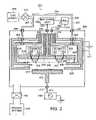
- FIG. 2illustrates a cross-sectional view of an embodiment of a magnetron sputtering apparatus 200 according to the present invention.
- the magnetron sputtering apparatus 200includes a chamber 202 , such as a vacuum chamber.
- the chamber 202is coupled in fluid communication to a vacuum system 204 through a vacuum control system 206 .
- the chamber 202is electrically coupled to ground potential.
- the chamber 202is coupled by one or more gas lines 207 to a feed gas source 208 .
- the gas lines 207are isolated from the chamber and other components by insulators 209 . Additionally, the gas lines 207 can be isolated from the feed gas source using in-line insulating couplers (not shown).
- a gas flow control system 210controls the gas flow to the chamber 202 .
- the gas source 208can contain any feed gas, such as argon.
- the feed gasincludes a mixture of gases.
- the feed gasincludes a reactive gas.
- a substrate 211 to be sputter coatedis supported in the chamber 202 by a substrate support 212 .
- the substrate 211can be any type of work piece such as a semiconductor wafer.
- the substrate support 212is electrically coupled to an output 213 of a bias voltage source 214 .
- An insulator 215isolates the bias voltage source 214 from a wall of the chamber 202 .
- the bias voltage source 214is an alternating current (AC) power source, such as a radio frequency (RF) power source.
- the substrate support 212is coupled to ground potential or is electrically floating.
- the magnetron sputtering apparatus 200also includes a cathode assembly 216 .
- the cathode assembly 216includes a cathode 218 and a sputtering target 220 composed of target material.
- the sputtering target 220is in contact with the cathode 218 .
- the sputtering target 220is positioned inside the cathode 218 .
- the distance from the sputtering target 220 to the substrate 211can vary from a few centimeters to about one hundred centimeters.
- the target materialcan be any material suitable for sputtering.
- the target materialcan be a metallic material, polymer material, superconductive material, magnetic material including ferromagnetic material, non-magnetic material, conductive material, non-conductive material, composite material, reactive material, or a refractory material.
- the cathode assembly 216is coupled to an output 222 of a matching unit 224 .
- An insulator 226isolates the cathode assembly 216 from a grounded wall of the chamber 202 .
- An input 230 of the matching unit 224is coupled to a first output 232 of a pulsed power supply 234 .
- a second output 236 of the pulsed power supply 234is coupled to an anode 238 .
- An insulator 240isolates the anode 238 from a grounded wall of the chamber 202 .
- Another insulator 242isolates the anode 238 from the cathode assembly 216 .
- the first output 232 of the pulsed power supply 234is directly coupled to the cathode assembly 216 (not shown).
- the second output 236 of the pulsed power supply 234is coupled to ground (not shown).
- the anode 238is also coupled to ground (not shown).
- the first output 232 of the pulsed power supply 234couples a negative voltage impulse to the cathode assembly 216 . In another embodiment (not shown), the first output 232 of the pulsed power supply 234 couples a positive voltage impulse to the anode 238 .
- the pulsed power supply 234generates peak voltage levels of up to about 30,000V. Typical operating voltages are generally between about 100V and 30 kV. In one embodiment, the pulsed power supply 234 generates peak current levels of less than one ampere to about 5,000 A or more depending on the size of the magnetron sputtering system. Typical operating currents varying from less than a few amperes to more than a few thousand amperes depending on the size of the magnetron sputtering system. In one embodiment, the power pulses have a repetition rate that is below 1 kHz. In one embodiment, the pulse width of the pulses generated by the pulsed power supply 234 is substantially between about one microsecond and several seconds.
- the anode 238is positioned so as to form a gap 244 between the anode 238 and the cathode assembly 216 that is sufficient to allow current to flow through a region 245 between the anode 238 and the cathode assembly 216 .
- the gap 244is between approximately 0.3 centimeters (0.3 cm) and ten centimeters (10 cm).
- the volume of region 245is determined by the area of the sputtering target 220 .
- the gap 244 and the total volume of region 245are parameters in the ionization process as will be discussed with reference to FIG. 3 .
- An anode shield 248is positioned adjacent to the anode 238 so as to protect the interior wall of the chamber 202 from being exposed to sputtered target material. Additionally, the anode shield 248 can function as an electric shield to electrically isolate the anode 238 from the plasma. In one embodiment, the anode shield 248 is coupled to ground potential. An insulator 250 is positioned to isolate the anode shield 248 from the anode 238 .
- the magnetron sputtering apparatus 200also includes a magnet assembly 252 .
- the magnet assembly 252is adapted to create a magnetic field 254 proximate to the cathode assembly 216 .
- the magnet assembly 252can include permanent magnets 256 , or alternatively, electro-magnets (not shown).
- the configuration of the magnet assembly 252can be varied depending on the desired shape and strength of the magnetic field 254 . In alternate embodiments, the magnet assembly can have either a balanced or unbalanced configuration.
- the magnet assembly 252includes switching electro-magnets, which generate a pulsed magnetic field proximate to the cathode assembly 216 .
- additional magnet assembliescan be placed at various locations throughout the chamber 202 to direct different types of sputtered target materials to the substrate 212 .
- the magnetron sputtering apparatus 200is operated by generating the magnetic field 254 proximate to the cathode assembly 216 .
- the permanent magnets 256continuously generate the magnetic field 254 .
- the magnetic field 254is generated by energizing a current source (not shown) that is coupled to electro-magnets.
- the strength of the magnetic field 254is between about one hundred and two thousand gauss.
- the pulsed power supply 234is a component in an ionization source that generates the weakly-ionized plasma.
- the pulsed power supplyapplies a voltage pulse between the cathode assembly 216 and the anode 238 .
- the pulsed power supply 234applies a negative voltage pulse to the cathode assembly 216 .
- the amplitude and shape of the voltage pulseare such that a weakly-ionized plasma is generated in the region 246 between the anode 238 and the cathode assembly 216 .
- the weakly-ionized plasmais also referred to as a pre-ionized plasma.
- the peak plasma density of the pre-ionized plasmais between about 10 6 and 10 12 cm ⁇ 3 for argon feed gas.
- the pressure in the chambercan vary from about 10 ⁇ 3 to 10 Torr.
- the peak plasma density of the pre-ionized plasmadepends on the properties of the specific magnetron sputtering system and is a function of the location of the measurement in the pre-ionized plasma.
- the pulsed power supply 234generates a low power pulse having an initial voltage of between about one hundred volts and five kilovolts with a discharge current of between about 0.1 amperes and one hundred amperes in order to generate the weakly-ionized plasma.
- the width of the pulsecan be in on the order of 0.1 microseconds up to one hundred seconds. Specific parameters of the pulse are discussed herein in more detail in connection with FIG. 4 and FIG. 5 .
- the pulsed power supply 234prior to the generating of the weakly-ionized plasma, the pulsed power supply 234 generates a potential difference between the cathode assembly 216 and the anode 238 before the feed gas is supplied between the cathode assembly 216 and the anode 238 .
- a direct current (DC) power supply(not shown) is used to generate and maintain the weakly-ionized or pre-ionized plasma.
- the DC power supplyis adapted to generate a voltage that is large enough to ignite the pre-ionized plasma.
- the DC power supplygenerates an initial voltage of several kilovolts with a discharge current of several hundred milliamps between the cathode assembly 216 and the anode 238 in order to generate and maintain the pre-ionized plasma.
- the value of the currentdepends on the power level generated by the power supply and is a function of the size of the magnetron. Additionally, the presence of a magnetic field in the region 245 can have a dramatic effect on the value of the applied voltage and current required to generate the weakly-ionized plasma.
- the DC power supplygenerates a current that is between about 1 mA and 100 A depending on the size of the magnetron and the strength of a magnetic field in the region 245 .
- the DC power supplybefore generating the weakly-ionized plasma, is adapted to generate and maintain an initial voltage between the cathode assembly 216 and the anode 238 before the introduction of the feed gas.
- the pre-ionized or weakly-ionized plasmacan be generated by numerous other techniques including UV radiation techniques, X-ray techniques, electron beam techniques, ion beam techniques, or ionizing filament techniques, for example.
- an alternating current (AC) power supplycan be used.
- an AC power supplycan require less power to generate a weakly-ionized plasma than a DC power supply.
- Forming a weakly-ionized or pre-ionized plasmasubstantially eliminates the probability of establishing a breakdown condition in the chamber 202 when high-power pulses are applied between the cathode assembly 216 and the anode 238 .
- the probability of establishing a breakdown conditionis substantially eliminated because the weakly-ionized plasma has a low-level of ionization that provides electrical conductivity through the plasma. This conductivity substantially prevents the formation of a breakdown condition, even when high power is applied to the plasma.
- high-power pulsesare then generated between the cathode assembly 216 and the anode 238 .
- the pulsed power supply 234generates the high-power pulses.
- the desired power level of the high-power pulsedepends on several factors including the desired deposition rate, the density of the pre-ionized plasma, and the size of the magnetron, for example.
- the power level of the high-power pulseis in the range of about one kilowatt to about ten megawatts or more. This power level range corresponds to target densities that are on the order of 0.01 kilowatt per square centimeter to more than ten kilowatts per square centimeter.
- Each of the high-power pulsesare maintained for a predetermined time that, in alternate embodiments, is approximately one microsecond to ten seconds.
- the repetition frequency or repetition rate of the high-power pulsesin one embodiment, is in the range of between about 0.1 Hz to 1 kHz.
- the average power generated by the pulsed power supply 234can be less than one megawatt depending on the size of the magnetron.
- the thermal energy in the sputtering target 220is conducted away or dissipated by liquid or gas cooling such as helium cooling (not shown).
- the high-power pulsesgenerate a strong electric field between the cathode assembly 216 and the anode 238 .
- This strong electric fieldis substantially located in the region 245 that is in the gap 244 between the cathode assembly 216 and the anode 238 .
- the electric fieldis a pulsed electric field.
- the electric fieldis a quasi-static electric field.
- quasi-static electric fieldwe mean an electric field that has a characteristic time of electric field variation that is much greater than the collision time for electrons with neutral gas particles. Such a time of electric field variation can be on the order of ten seconds. The strength and the position of the strong electric field will be discussed in more detail with reference to FIG. 3 .
- the high-power pulsesgenerate a highly-ionized or a strongly-ionized plasma from the weakly-ionized plasma.
- the discharge current density that is formed from this strongly-ionized plasmacan be as high as about five-hundred amperes per squared centimeter or more for a pressure that is as high as about ten Torr. Since the sputtering target 220 is typically negatively biased, the positively charged ions in the strongly-ionized plasma accelerate at high velocity towards the sputtering target 220 . The accelerated ions impact the surface of the sputtering target 220 , causing the target material to be sputtered.
- the strongly-ionized plasma of the present inventionresults in a very high sputtering rate of the target material.
- the strongly-ionized plasmatends to diffuse homogenously in the region 246 .
- the homogenous diffusionresults in accelerated ions impacting the surface of the sputtering target 220 in a more uniform manner than with conventional magnetron sputtering. Consequently, the surface of the sputtering target 220 is eroded more evenly and, thus higher target utilization is achieved.
- the target materialis sputtered more uniformly across the surface of the sputtering target 220 , the uniformity and homogeneity of the material deposited on the substrate 211 is also increased without the necessity of rotating the substrate 211 and/or the magnet assembly 252 .
- the physical mechanism responsible for this homogenous diffusionis described with reference to FIG. 6A through FIG. 6D .
- the high-power pulsed magnetron sputtering system 200 of the present inventiongenerates a relatively high electron temperature plasma and a relatively high density plasma.
- One application for the high-power pulsed magnetron sputtering system 200 of the present inventionis ionized physical vapor deposition (IPVD), which is a technique that converts neutral sputtered atoms into positive ions to enhance the sputtering process.
- IPVDphysical vapor deposition
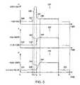
- FIG. 3illustrates a cross-sectional view of the cathode assembly 216 and the anode 238 of FIG. 2 .
- the strong electric field 260is located in the region 245 between the cathode assembly 216 and the anode 238 .
- the strong electric field 260facilitates a multi-step ionization process that substantially increases the rate at which the strongly-ionized plasma is formed.
- the feed gas 264flows between the cathode assembly 216 and the anode 238 .
- a pre-ionizing voltageis applied between the cathode assembly 216 and the anode 238 across the feed gas 264 which forms the weakly-ionized plasma.
- the weakly-ionized plasmais generally formed in the region 245 and diffuses to a region 266 as the feed gas 264 continues to flow.
- the electrons in the weakly-ionized plasmaare substantially trapped in the region 266 by the magnetic field 254 .
- the magnetic field 254is generated in the region 245 to substantially trap electrons where the weakly-ionized plasma is ignited.
- a high-power pulseis then applied between the cathode assembly 216 and the anode 238 .
- This high-power pulsegenerates the strong electric field 260 in the region 245 between the cathode assembly 216 and the anode 238 .
- the strong electric field 260results in collisions occurring between neutral atoms and ions in the weakly ionized plasma. These collisions generate numerous excited atoms in the weakly-ionized plasma.
- the accumulation of excited atoms in the weakly-ionized plasmaalters the ionization process.
- the strongly-ionized plasmais generated by a multi-step ionization process having an efficiency that increases as the density of excited atoms in the weakly-ionized plasma increases.
- the distance or gap 244 between the cathode assembly 216 and the anode 238is chosen so as to maximize the rate of excitation of the atoms.
- the value of the electric field 260 in the region 245depends on the voltage level applied by the pulsed power supply 234 ( FIG. 2 ) and the size of the gap 244 between the anode 238 and the cathode assembly 216 .
- the strength of the electric field 260can vary between about 10V/cm and 10 5 V/cm depending on various parameters and operating conditions of the magnetron system.
- the gap 244can be between about 0.30 cm and about 10 cm depending on various parameters of the process.
- the electric field 260 in the region 245is rapidly applied to the pre-ionized or weakly-ionized plasma.
- the rapidly applied electric field 260is generated by a voltage pulse having a rise time that is between about 0.1 microsecond and ten seconds.
- the dimensions of the gap 244 and the parameters of the applied electric field 260are varied in order to determine the optimum condition for a relatively high rate of excitation of the atoms in the region 245 .
- an argon atomrequires an energy of about 11.55 eV to become excited.
- the weakly-ionized plasmais formed and the atoms in the weakly-ionized plasma undergo a stepwise ionization process.
- the excited atoms in the weakly-ionized plasmathen encounter the electrons that are trapped in the region 266 by the magnetic field 254 .
- excited atomsonly require about 4 eV of energy to ionize while neutral atoms require about 15.76 eV of energy to ionize, the excited atoms will ionize at a much higher rate than neutral atoms.
- ions in the strongly-ionized plasmabombard the sputtering target 220 causing secondary electron emission from the sputtering target 220 . These secondary electrons are substantially trapped by the magnetic field 254 and interact with any neutral or excited atoms in the strongly-ionized plasma. This process further increases the density of ions in the strongly-ionized plasma as the feed gas 264 is replenished.
- the multi-step ionization process corresponding to the rapid application of the electric field 260can be described as follows: Ar+e ⁇ ⁇ Ar*+e ⁇ Ar*+e ⁇ ⁇ Ar + +2e ⁇
- Arrepresents a neutral argon atom in the feed gas and e ⁇ represents an ionizing electron generated in response to a pre-ionized plasma, when sufficient voltage is applied between the cathode assembly 216 and the anode 238 .
- Ar*represents an excited argon atom in the weakly-ionized plasma. The collision between the excited argon atom and the ionizing electron results in an argon ion (Ar + ) and two electrons.
- the excited argon atomsgenerally require less energy to become ionized than neutral argon atoms.
- the excited atomstend to more rapidly ionize near the surface of the sputtering target 220 than the neutral argon atoms.
- the efficiency of the ionization processrapidly increases. The increased efficiency eventually results in an avalanche-like increase in the density of the strongly-ionized plasma.
- the proportion of the energy applied to the weakly-ionized plasma which is transformed to the excited atomsis very high for a pulsed discharge in the feed gas.
- high power pulsesare applied to a weakly-ionized plasma across the gap 244 to generate a strong electric field between the anode 238 and the cathode assembly 216 .
- This strong electric fieldgenerates excited atoms in the weakly-ionized plasma.
- the excited atomsare rapidly ionized by secondary electrons emitted by the sputtering target 220 .
- This rapid ionizationresults in a strongly-ionized plasma having a large ion density being formed in an area proximate to the cathode assembly 216 .
- FIG. 4illustrates a graphical representation 300 of the applied power of a pulse as a function of time for periodic pulses applied to the plasma in the magnetron sputtering system of FIG. 2 .
- the feed gas from the gas source 208flows into the chamber 202 before the pulsed power supply 234 is activated.
- the time required for a sufficient quantity of gas to flow from the gas source 208 into the chamber 202depends on several factors including the flow rate of the gas and the desired pressure in the chamber 202 .
- the pulsed power supply 234is activated before the feed gas flows into the chamber 202 .
- the feed gasis injected between the anode 238 and the cathode assembly 216 where it is ignited by the pulsed power supply 234 to generate the weakly-ionized plasma.
- the feed gasflows between the anode 238 and the cathode assembly 216 between time t 0 and time t 1 .
- the pulsed power supply 234generates a pulse 302 between the cathode assembly 216 and the anode 238 that has a power level between about 0.01 kW and 100 kW depending on the size of the magnetron.
- the pulse 302is sufficient to ignite the feed gas to generate the weakly-ionized plasma.
- the pulsed power supply 234applies a potential in the gap 244 between the cathode assembly 216 and the anode 238 before the feed gas from the gas source 208 is delivered into the chamber 202 .
- the feed gasis ignited as it flows between the cathode assembly 216 and the anode 238 .
- the pulsed power supply 234generates the pulse 302 between the cathode assembly 216 and the anode 238 when the feed gas from the gas source 208 is delivered into the chamber 202 .
- the power generated by the pulsed power supply 234partially ionizes the gas that is located in the region 245 between the cathode assembly 216 and the anode 238 .
- the partially ionized gasis also referred to as a weakly-ionized plasma or a pre-ionized plasma.
- the formation of weakly-ionized plasmasubstantially eliminates the possibility of creating a breakdown condition when high-power pulses are applied to the weakly-ionized plasma.
- the poweris continuously applied for between about one microsecond and one hundred seconds to allow the pre-ionized plasma to form and be maintained at a sufficient plasma density.
- the power from the pulsed power supply 234is continuously applied after the weakly-ionized plasma is ignited to maintain the weakly-ionized plasma.
- the pulsed power supply 234can be designed so as to generate a continuous nominal power in order to generate and sustain the weakly-ionized plasma until a high-power pulse is delivered by the pulsed power supply 234 .
- the pulsed power supply 234delivers a high-power pulse 304 across the weakly-ionized plasma.
- the high-power pulse 304has a power that is in the range of between about one kilowatt to ten megawatts depending on the size of the magnetron.
- the high-power pulsehas a leading edge 306 with a rise time that is between about 0.1 microseconds and ten seconds
- the high-power pulse 304has a power and a pulse width that is sufficient to transform the weakly-ionized plasma to a strongly-ionized plasma.
- the high-power pulse 304is applied for a time that is in the range of between about ten microseconds and ten seconds. At time t 4 , the high-power pulse 304 is terminated.
- the power supply 224maintains the weakly-ionized plasma after the delivery of the high-power pulse 304 by applying background power that, in one embodiment, is between about 0.01 kW and 100 kW.
- the background powercan be a pulsed or continuously applied power that maintains the pre-ionization condition in the plasma, while the pulsed power supply 234 prepares to deliver another high-power pulse 308 .
- the pulsed power supply 234delivers another high-power pulse 308 .
- the repetition rate between the high-power pulses 304 , 308is, in one embodiment, between about 0.1 Hz and 1 kHz.
- the particular size, shape, width, and frequency of the high-power pulses 304 , 308depend on various factors including process parameters, the design of the pulsed power supply 234 , the size of the magnetron, and the design of the sputter system.
- the shape and duration of the leading edge 308 and the trailing edge 310 of the high-power pulse 304is chosen to sustain the weakly-ionized plasma while controlling the rate of ionization of the strongly-ionized plasma.
- the particular size, shape, width, and frequency of the high-power pulse 304is chosen to control the rate of sputtering of the target material.
- FIG. 5illustrates graphical representations 320 , 322 , and 324 of the absolute value of applied voltage, current, and power, respectively, as a function of time for periodic pulses applied to the plasma in the magnetron sputtering system of FIG. 2 .
- the feed gas from the gas source 208flows into the chamber 202 before the pulsed power supply 234 is activated.
- the time required for a sufficient quantity of gas to flow from the gas source 208 into the chamber 202depends on several factors including the flow rate of the gas and the desired pressure in the chamber 202 .
- the power supply 238generates a constant power.
- the pulsed power supply 234generates a voltage 326 across the anode 238 and the cathode assembly 216 .
- the voltage 326is approximately between one hundred and two thousand volts.
- the period between time t 0 and time t 1can be on the order of several microseconds up to several milliseconds.
- the current 328 and the power 330have constant value.
- the voltage 326 at time t 2is between about 100V and 2,000V.
- the current 334 at time t 2is between about 0.1 A and 100 A.
- the power 336 delivered at time t 2is between about 0.01 kW and 100 kW.
- the power 336 generated by the pulsed power supply 234partially ionizes the gas that is located between the cathode assembly 216 and the anode 238 .
- the partially ionized gasis also referred to as a weakly-ionized plasma or a pre-ionized plasma.
- the formation of weakly-ionized plasmasubstantially eliminates the possibility of creating a breakdown condition when high-power pulses are applied to the weakly-ionized plasma.
- the suppression of this breakdown conditionsubstantially eliminates the occurrence of undesirable arcing in the chamber 202 .
- the period between time t 1 and time t 2is between about one microsecond and one hundred seconds to allow the pre-ionized plasma to form and be maintained at a sufficient plasma density.
- the power 336 from the pulsed power supply 234is continuously applied to maintain the weakly-ionized plasma.
- the pulsed power supply 234can be designed so as to output a continuous nominal power into order to sustain the weakly-ionized plasma.
- the pulsed power supply 234delivers a large voltage pulse 338 across the weakly-ionized plasma.
- the large voltage pulse 338has a voltage that is in the range of two hundred to thirty thousand volts.
- the period between time t 2 and time t 3is between about 0.1 microseconds and ten seconds.
- the large voltage pulse 338is applied between time t 3 and time t 4 , before the current across the plasma begins to increase.
- the time period between time t 3 and time t 4can be between about one microsecond and ten seconds.
- time t 4 and time t 5the voltage 340 drops as the current 342 increases.
- the power 344also increases between time t 4 and time t 5 , until a quasi-stationary state exists between the voltage 346 and the current 348 .
- the period between time t 4 and time t 5can be on the order of one to one hundred microseconds.
- the voltage 346is between about one hundred and thirty thousand volts
- the current 348is between about one hundred and five thousand amperes
- the power 350is between about one kilowatt and ten megawatts.
- the power 350is continuously applied to the plasma until time t 6 .
- the period between time t 5 and time t 6is approximately between one microsecond and ten seconds.
- the pulsed power supply 234delivers a high-power pulse having a maximum power 350 and a pulse width that is sufficient to transform the weakly-ionized plasma to a strongly-ionized plasma. At time t 6 , the maximum power 350 is terminated. In one embodiment, the pulsed power supply 234 continues to supply a background power that is sufficient to maintain the plasma after time t 6 .
- the power supply 234maintains the plasma after the delivery of the high-power pulse by continuing to apply a power 352 that can be between about 0.01 kW and 100 kW to the plasma.
- the continuously generated powermaintains the pre-ionization condition in the plasma, while the pulsed power supply 234 prepares to deliver the next high-power pulse.
- the pulsed power supply 234delivers the next high-power pulse (not shown).
- the repetition rate between the high-power pulsesis between about 0.1 Hz and 1 kHz.
- the particular size, shape, width, and frequency of the high-power pulsesdepend on various factors including process parameters, the design of the pulsed power supply 234 , the size of the magnetron, and the design of the sputter system.
- the power supply 234generates a constant voltage.
- the applied voltage 320is continuously applied from time t 2 until time t 6 .
- the current 322 and the power 324change to keep the applied voltage 320 constant.
- the current 322 and the power 224rise until time t 6 , where the voltage 320 is terminated.
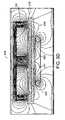
- FIG. 6A through FIG. 6Dillustrate various simulated magnetic field distributions 400 , 402 , 404 , and 406 that are proximate to the cathode assembly 116 for various electron ExB drift currents in the magnetron sputtering apparatus 200 of FIG. 2 .
- the simulated magnetic fields distributions 400 , 402 , 404 , and 406indicate that high-power plasmas having high current density tend to diffuse homogeneously in the area 246 of the magnetron sputtering apparatus 200 of FIG. 2 .
- the high-power pulses between the cathode assembly 216 and the anode 238generate secondary electrons from the cathode assembly 216 that move in a substantially circular motion proximate to the cathode assembly 216 according to crossed electric and magnetic fields.
- the substantially circular motion of the electronsgenerate an electron E ⁇ B drift current.
- the magnitude of the electron E ⁇ B drift currentis proportional to the magnitude of the discharge current in the plasma and, in one embodiment, is approximately in the range of between about three and ten times the magnitude of the discharge current.
- the substantially circular electron E ⁇ B drift currentgenerates a magnetic field that interacts with the magnetic field generated by the magnet assembly 252 .
- the magnetic field generated by the electron ExB drift currenthas a direction that is substantially opposite to the direction of the magnetic field generated by the magnet assembly 252 .
- the magnitude of the magnetic field generated by the electron E ⁇ B drift currentincreases with increased electron E ⁇ B drift current.
- the homogeneous diffusion of the strongly-ionized plasma in the region 246is caused, at least in part, by the interaction of the magnetic field generated by the magnet assembly 252 and the magnetic field generated by the electron E ⁇ B drift current.
- the electron E ⁇ B drift currentdefines a substantially circular shape for low current density plasma.
- the substantially circular electron E ⁇ B drift currenttends to describe a more complex shape as the interaction of the magnetic field generated by the magnet assembly 252 , the electric field generated by the high-power pulse, and the magnetic field generated by the electron E ⁇ B drift current becomes more acute.
- the electron E ⁇ B drift currenthas a substantially cycloidal shape.
- the exact shape of the electron E ⁇ B drift currentcan be quite elaborate and depends on various factors.
- FIG. 6Aillustrates the magnetic field lines 408 produced from the interaction of the magnetic field generated by the magnet assembly 252 and the magnetic field generated by an electron E ⁇ B drift current 410 illustrated by a substantially circularly shaped ring.
- the electron E ⁇ B drift current 410is generated proximate to the cathode assembly 216 .
- the electron E ⁇ B drift current 410is approximately one hundred amperes (100 A). In one embodiment of the invention, the electron E ⁇ B drift current 410 is between approximately three and ten times as great as the discharge current. Thus, in the example shown in FIG. 6A , the discharge current is approximately between 10 A and 30 A.
- the magnetic field lines 408 shown in FIG. 6Aindicate that the magnetic field generated by the magnet assembly 252 is substantially undisturbed by the relatively small magnetic field that is generated by the relatively small electron E ⁇ B drift current 410 .
- FIG. 6Billustrates the magnetic field lines 412 produced from the interaction of the magnetic field generated by the magnet assembly 252 and the magnetic field generated by an electron E ⁇ B drift current 414 .
- the electron E ⁇ B drift current 414is generated proximate to the cathode assembly 216 .
- the electron E ⁇ B drift current 414is approximately 300 A. Since the electron E ⁇ B drift current 414 is typically between about three and ten times as great as the discharge current, the discharge current in this example is approximately between 30 A and 100 A.
- the magnetic field lines 412 that are generated by the magnet assembly 252are substantially undisturbed by the relatively small magnetic field generated by the relatively small electron E ⁇ B drift current 414 .
- the magnetic field lines 416 that are closest to the electron E ⁇ B drift current 414are somewhat distorted by the magnetic field generated by the electron E ⁇ B drift current 414 . The distortion suggests that a larger electron E ⁇ B drift current should generate a stronger magnetic field that will interact more strongly with the magnetic field generated by the magnet assembly 252 .
- FIG. 6Cillustrates the magnetic field lines 418 that are produced from the interaction of the magnetic field generated by the magnet assembly 252 and the magnetic field generated by an electron E ⁇ B drift current 420 .
- the electron E ⁇ B drift current 420is generated proximate to the cathode assembly 216 .
- the electron E ⁇ B drift current 420is approximately 1,000 A. Since the electron E ⁇ B drift current 420 is typically between about three and ten times as great as the discharge current, the discharge current in this example is approximately between 100 A and 300 A.
- the magnetic field lines 418 that are generated by the magnet assembly 252exhibit substantial distortion that is caused by the relatively strong magnetic field generated by the relatively large electron E ⁇ B drift current 420 .
- the larger electron E ⁇ B drift current 420generates a stronger magnetic field that strongly interacts with and can begin to dominate the magnetic field generated by the magnet assembly 252 .
- the magnetic field lines 422allow the strongly-ionized plasma to more uniformly distribute itself in the area 246 .
- the strongly-ionized plasmais substantially uniformly diffused in the area 246 , and consequently, the sputtering target 220 is eroded more uniformly thereby resulting in higher target utilization than can be achieved than in conventional magnetron sputtering systems.
- FIG. 6Dillustrates the magnetic field lines 424 produced from the interaction of the magnetic field generated by the magnet assembly 252 and the magnetic field generated by an electron E ⁇ B drift current 426 .
- the electron E ⁇ B drift current 426is generated proximate to the cathode assembly 216 .
- the electron E ⁇ B drift current 426is approximately 5,000 A.
- the discharge current in this exampleis approximately between 500 A and 1,700 A.
- the magnetic field lines 424 generated by the magnet assembly 252are relatively distorted due to their interaction with the relatively strong magnetic field generated by the relatively large electron E ⁇ B drift current 426 .
- the relatively large electron E ⁇ B drift current 426generates a very strong magnetic field that is substantially stronger than the magnetic field generated by the magnet assembly 252 .
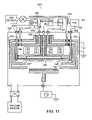
- FIG. 7illustrates a cross-sectional view of another embodiment of a magnetron sputtering apparatus 450 according to the present invention.
- the magnetron sputtering apparatus 450includes an electrode 452 that generates a weakly-ionized or pre-ionized plasma.
- the electrode 452is also referred to as a pre-ionizing filament electrode and is a component in an ionization source that generates the weakly ionized plasma.
- the electrode 452is coupled to an output 454 of a power supply 456 .
- the power supply 456can be a DC power supply or an AC power supply.
- An insulator 458isolates the electrode 452 from the grounded wall of the chamber 202 .
- the electrode 452is substantially shaped in the form of a ring electrode. In other embodiments, the electrode 452 is substantially shaped in a linear form or any other shape that is suitable for pre-ionizing the plasma.
- a second output 460 of the power supply 456is coupled to the cathode 218 .
- the insulator 226isolates the cathode 218 from the grounded wall of the chamber 202 .
- the power supply 456generates an average output power that is in the range of between about 0.01 kW and 100 kW. Such an output power is sufficient to generate a suitable current between the electrode 452 and the cathode assembly 216 to pre-ionize feed gas that is located proximate to the electrode 452 .
- the magnetron sputtering apparatus 450functions in a similar manner to the magnetron sputtering apparatus 200 of FIG. 2 , but with some operational differences.
- the magnetic field 254is generated proximate to the cathode assembly 216 .
- the strength of the magnetic field 254is between about one hundred and two thousand gauss.
- the feed gasis supplied from the gas source 208 to the chamber 202 by the gas flow control system 210 .
- the power supply 456applies a suitable current between the cathode assembly 216 and the electrode 452 .
- the parameters of the currentare chosen to establish a weakly-ionized plasma in the area 246 proximate to the electrode 452 .
- the power supply 456generates a voltage of between about one hundred volts and five thousand volts with a discharge current that is between about 0.1 A and 100 A depending on the size of the magnetron. An example with specific parameters will be discussed herein in more detail in connection with FIG. 8 .
- the resulting pre-ionized plasma densityis in the range between approximately 10 6 and 10 12 cm ⁇ 3 for argon sputtering gas.
- the pressure in the chamber 202is in the range of approximately 10 ⁇ 3 to 10 Torr.
- the weakly-ionized or pre-ionized plasmareduces or substantially eliminates the possibility of establishing a breakdown condition in the chamber 202 when high-power pulses are applied to the plasma.
- the pulsed power supply 234then generates a high-power pulse between the cathode assembly 216 and the anode 238 .
- the high-power pulsegenerates a strongly-ionized plasma from the weakly-ionized plasma.
- the parameters of the high-power pulsedepend on various parameters including the size of the magnetron, the desired deposition rate, and the concentration of the pre-ionized plasma necessary for depositing the target material.
- the high-power pulse between the cathode assembly 216 and the anode 238is in the range of about one kilowatt to about ten megawatts. This corresponds to target densities on the order of several kilowatts per square centimeter. In one embodiment, the ion current density that can be generated from the strongly-ionized plasma is greater than about one ampere per squared centimeter for a pressure of approximately ten mTorr.
- the high-power pulsehas a pulse width that is in the range of approximately one microsecond to several seconds. In one embodiment, the repetition rate of the high-power discharge is in the range of between about 0.1 Hz to 1 kHz. In one embodiment, in order to minimize undesirable target heating, the average power generated by the pulsed power supply is less than one megawatt depending on the size of the magnetron. In one embodiment, the thermal energy in the sputtering target 220 is conducted away or dissipated by liquid or gas cooling (not shown).
- the gas flow control system 210provides a feed gas flow rate that is high enough to maintain the strongly-ionized plasma. Additionally, the vacuum control system 206 controls the pressure so as to maintain the pressure inside the chamber 202 in a range that supports the strongly-ionized plasma.
- the ions in the strongly-ionized plasmaaccelerate towards the sputtering target 220 at high velocity and impact the surface of the sputtering target 220 .
- the strongly ionized plasmacauses a very high sputtering rate of the target material.
- the strongly-ionized plasma generated by the sputtering systems according to the present inventiontends to diffuse homogenously in the area 246 due to the interaction of generated magnetic fields. This homogenous diffusion results in a more uniform distribution of ions impacting the surface of the target material 220 compared with conventional magnetron sputtering systems, thereby resulting in relatively high target utilization and relatively uniform deposition of target material on the substrate 211 .
- FIG. 8illustrates a graphical representation of pulse power as a function of time for periodic pulses applied to the plasma in the magnetron sputtering system of FIG. 7 .
- the feed gas from the gas source 208flows into the chamber 202 at time t 0 , before either the power supply 456 or the pulsed power supply 234 are activated.
- the power supply 456 and/or the pulsed power supply 234are activated at time t 0 before the gas enters the chamber 202 .
- the feed gasis injected between the electrode 452 and the cathode assembly 216 where it is ignited by the power supply 456 to generate the weakly-ionized plasma.
- the time required for a sufficient quantity of gas to flow into the chamber 202depends on several factors including the flow rate of the gas and the desired operating pressure in the chamber 202 .
- the power supply 456generates a power 502 that is in the range of between about 0.01 kW to about 100 kW between the electrode 452 and the cathode assembly 216 .
- the power 502causes the gas proximate to the electrode 452 to become partially ionized, thereby generating a weakly-ionized plasma or a pre-ionized plasma.
- the pulsed power supply 234delivers a high-power pulse 504 to the weakly-ionized plasma that is on the order of less than one kilowatt to about ten megawatts depending on the size of the magnetron.
- the high-power pulse 504is sufficient to transform the weakly-ionized plasma to a strongly-ionized plasma.
- the high-power pulsehas a leading edge 506 having a rise time that is between about 0.1 microseconds and ten seconds.
- the pulse width of the high-power pulse 504is in the range of between about one microsecond and ten seconds.
- the high-power pulse 504is terminated at time t 4 .
- the power 502 from the power supply 456is continuously applied to sustain the pre-ionized plasma, while the pulsed power supply 234 prepares to deliver another high-power pulse 508 .
- the power supply 456is an AC power supply and delivers suitable power pulses to ignite and sustain the weakly-ionized plasma.
- the pulsed power supply 234delivers another high-power pulse 508 .
- the repetition rate of the high-power pulsescan be between about 0.1 Hz and 1 kHz.
- the particular size, shape, width, and frequency of the high-power pulsedepend on the process parameters and on the design of the pulsed power supply 234 and the sputter system.
- the shape and duration of the leading edge 506 and the trailing edge 510 of the high-power pulse 504is chosen to control the rate of ionization of the strongly-ionized plasma.
- the particular size, shape, width, and frequency of the high power pulse 504is chosen to control the rate of sputtering of the target material.
- FIG. 9A through FIG. 9Care cross-sectional views of various embodiments of cathode assemblies 216 ′, 216 ′′, and 216 ′′′ according to the present invention.
- FIG. 9A through FIG. 9Cillustrate one side (the right side with reference to FIG. 7 ) of each cathode assembly. The left side of each cathode assembly is generally symmetrical to the illustrated right side.
- FIG. 9A through FIG. 9Cillustrate various configurations of the electrode 452 and the cathode assemblies 216 ′, 216 ′′, and 216 ′′′. These various configurations can affect the parameters of the electric field generated between the electrode 452 and each of the cathode assemblies 216 ′, 216 ′′, and 216 ′′′.
- the parameters of the electric fieldcan influence the ignition of the pre-ionized plasma as well as the pre-ionization process generally.
- these various embodimentscreate the necessary conditions for breakdown of the feed gas and ignition of the weakly-ionized plasma in the region between the anode 238 and each respective cathode assembly 216 ′, 216 ′′, and 216 ′′′.
- FIG. 9Aillustrates one side of the cathode assembly 216 ′.
- a sputtering target 220 ′is substantially positioned in contact with a cathode 218 ′.
- the sputtering target 220 ′extends past the bend 520 of the ring-shaped electrode 452 .
- the electric field lines (not shown) from the electric field generated between the cathode assembly 216 ′ and the ring-shaped electrode 452are substantially perpendicular to the cathode assembly 216 ′ along the circumference of the ring-shaped electrode 452 .
- This embodimentcan increase the efficiency of the pre-ionization process.
- the cathode 218 ′is never directly exposed to the plasma, ions from the plasma do not bombard the cathode 218 ′ and therefore, any contamination that could otherwise be generated by the cathode material is substantially reduced.
- FIG. 9Billustrates one side of the cathode assembly 216 ′′.
- a sputtering target 220 ′′is substantially positioned in contact with a cathode 218 ′′.
- the sputtering target 220 ′′extends to the point 524 on the cathode assembly 216 ′′.
- the electric field lines (not shown) generated between the cathode assembly 216 ′′ and the electrode 452are substantially perpendicular to the cathode assembly 216 ′′ at the point 528 on the cathode 218 ′′.
- the electric field in the gap 530 between the electrode 452 and the cathode 218 ′′is adapted to ignite the plasma from the feed gas flowing through the gap 530 .
- this embodimentcan increase the efficiency of the pre-ionization process.
- FIG. 9Cillustrates one side of the cathode assembly 216 ′′′.
- a sputtering target 220 ′′′is substantially positioned in contact with a cathode 218 ′′′.
- the sputtering target 220 ′′′extends to position 532 on the cathode assembly 216 ′′′.
- the electric field lines (not shown) generated between the cathode assembly 216 ′′′ and the electrode 452are substantially perpendicular to the cathode assembly 216 ′′′ at the position 538 .
- the electric field in the gap 540 between the electrode 452 and the cathode 218 ′′′is adapted to ignite the plasma from the feed gas flowing through the gap 540 .
- this embodimentcan increase the efficiency of the pre-ionization process.
- FIG. 10is a cross-sectional view of another embodiment of a magnetron sputtering apparatus 450 ′ according to the present invention.
- This embodimentis similar to the magnetron sputtering apparatus 450 of FIG. 7 .
- the electrode 452 ′which is a component of the ionization source, substantially surrounds the cathode assembly 216 .
- the position of the electrode 452 ′ relative to the cathode assembly 216is chosen to achieve particular electrical conditions in the gap 244 between the anode 238 and the cathode assembly 216 .
- the pre-ionizing electrode 452 ′since the pre-ionizing electrode 452 ′ is not physically located in the region 245 ′ between the anode 238 and the cathode assembly 216 , it does not interfere with the strong electric field that results when a high-power pulse is applied between the anode 238 and the cathode assembly 216 . Additionally, the location of the pre-ionizing electrode 452 ′ results in a more uniformly distributed weakly-ionized plasma in the region 246 ′.
- the power supply 456applies a substantially constant voltage between the cathode assembly 216 and the electrode 452 ′.
- the substantially constant voltagegenerates a weakly-ionized or pre-ionized plasma proximate to the electrode 452 ′ and the cathode assembly 216 .
- the pre-ionized plasmasubstantially eliminates the possibility of establishing a breakdown condition in the chamber 202 when high-power pulses are applied to the plasma.
- the power supply 456is a DC power supply that generates a DC voltage that is in the range of between about one hundred volts and several kilovolts with a discharge current that is in the range of between about 0.1 A and 100 A.
- the power supply 456is an AC power supply that generates voltage pulses between the cathode assembly 216 and the electrode 452 ′.
- a distance 462 between the electrode 452 ′ and the cathode 218can be varied by changing the diameter of the electrode 452 ′.
- the distance 462can be varied from about 0.1 cm to about 10 cm.
- the distance 462is optimized to generate sustainable weakly-ionized plasma in the region 246 ′.
- the vertical position of the electrode 452 ′ relative to the cathode assembly 216can also be varied.
- FIG. 11illustrates a cross-sectional view of another illustrative embodiment of a magnetron sputtering apparatus 450 ′′ according to the present invention.
- the magnetron sputtering apparatus 450 ′′is similar to the magnetron sputtering apparatus 450 of FIG. 7 .
- the electrode 452 ′′is a component of an ionization source. However, the electrode 452 ′′ is coupled to a first power supply 464 and also to an additional second power supply 466 .
- the position of the electrode 452 ′′ relative to the cathode assembly 216is chosen to achieve particular sputtering characteristics.
- a first output 468 of the first power supply 464is coupled through the insulator 458 to a first side 470 of the electrode 452 ′′.
- a second output 472 of the first power supply 464is coupled to a second side 474 of the electrode 452 ′′ through an insulator 476 .
- the first power supply 464is adapted to generate a current through the electrode 452 ′′.
- the currentessentially generates heat in the electrode 452 ′′.
- the heated electrode 452 ′′emits electrons in the area 245 ′′.
- the first power supply 464is a DC power supply and applies a substantially constant current through the electrode 452 ′′. In another embodiment, the first power supply 464 is an AC power supply.
- a first output 478 of the second power supply 466is coupled to the anode 238 through an insulator 480 .
- a second output 482 of the second power supply 466is coupled to the second side 474 of the electrode.
- the second power supply 466is adapted to apply a voltage between the electrode 452 ′′ and the anode 238 .
- the second power supply 466can be an AC power supply or a DC power supply. In one embodiment, the second power supply 466 generates a voltage in the range of about one hundred volts and several kilovolts with a discharge current that is in the range of between about 0.1 A and 10 A.
- the second power supply 466applies a substantially constant voltage that generates a weakly-ionized or pre-ionized plasma proximate to the electrode 452 ′′ and the cathode assembly 216 .
- the pre-ionized plasmasubstantially eliminates the possibility of establishing a breakdown condition in the chamber 202 when high-power pulses are applied to the plasma.
- the pulsed power supply 234then generates a high-power pulse between the cathode assembly 216 and the anode 238 .
- the high-power pulsegenerates a strongly-ionized plasma from the weakly-ionized plasma.
- the parameters of the high-power pulsedepend on various parameters including the size of the magnetron, the desired deposition rate, and the concentration of the pre-ionized plasma necessary for depositing the target material, for example.
- FIG. 12is a flowchart 600 of an illustrative process of sputter deposition according to the present invention.
- the processis initiated (step 602 ) by activating various systems in the magnetron sputtering apparatus 200 of FIG. 2 .
- the chamber 202is initially pumped down to a specific pressure (step 604 ).
- the pressure in the chamber 202is checked (step 606 ).
- feed gasis then pumped into the chamber (step 608 ).
- the gas pressureis then checked (step 610 ). If the gas pressure is correct, the chamber pressure is then re-checked (step 612 ). If the chamber pressure is correct, an appropriate magnetic field is generated proximate to the feed gas (step 614 ).
- the magnet assembly 252 of FIG. 2includes at least one permanent magnet, where magnetic field is generated constantly, even before the process is initiated.
- a magnetic assembly(not shown) includes at least one electromagnet, where the magnetic field is generated only when the electromagnet is operating.
- the feed gasis ionized to generate a weakly-ionized plasma (step 618 ).
- the weakly-ionized plasmacan be generated by creating a relatively low current discharge in the gap 244 between the cathode assembly 216 and the anode 238 of FIG. 2 .
- the weakly-ionized plasmacan be generated by creating a relatively low current discharge between the electrode 452 and the cathode assembly 216 of FIG. 7 .
- the electrode 452 ′′is heated to emit electrons proximate to the cathode assembly 216 of FIG. 11 . In the embodiment of FIG. 11 , a relatively low current discharge is created between the anode 238 and the electrode 452 ′′.
- the weakly-ionized plasmais generated by applying a potential across the gap 244 between the cathode assembly 216 and the anode 238 before the introduction of the feed gas.
- the weakly-ionized plasmais generated by applying a potential difference between the electrode 452 and the cathode assembly 216 before the introduction of the feed gas to generate the weakly-ionized plasma.
- a strongly-ionized plasmais generated from the weakly-ionized plasma (step 622 ).
- the strongly-ionized plasmais generated by applying a high-power pulse in the gap 244 between the cathode assembly 216 and the anode 238 .
- the high-power pulseresults in a strong electric field being generated in the gap 244 between the anode 238 and the cathode assembly 216 .
- the strong electric fieldresults in a stepwise ionization process.
- the strongly-ionized plasmais substantially homogeneous in the area 246 of FIG. 2 . This homogeneity results in substantially uniform erosion of the sputtering target 220 and, therefore, relatively high sputtering target utilization.
- the cathode assembly 216attracts ions from the strongly-ionized substantially uniform plasma because the cathode assembly 216 is negatively biased relative to the anode 238 . This causes the ions to bombard the cathode assembly 216 causing sputtering of the target material.
- the sputter depositionis monitored (step 628 ) by known monitoring techniques. Once the sputter deposition is completed (step 630 ), the sputter process is ended (step 632 ).
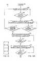
- FIG. 13includes FIGS. 13 A and 13 B which is a flowchart 650 of an illustrative process of controlling the sputter rate according to the present invention.
- the processis initiated (step 602 ) by activating various systems in the magnetron sputtering apparatus 200 of FIG. 2 .
- the chamber 202is initially pumped down to a specific pressure (step 604 ).
- the pressure in the chamber 202is evaluated (step 606 ).
- feed gasis then pumped into the chamber (step 608 ).
- the gas pressureis evaluated (step 610 ). If the gas pressure is correct, the pressure in the chamber 202 is again evaluated (step 612 ). If the pressure in the chamber 202 is correct, an appropriate magnetic field is generated proximate to the feed gas (step 614 ).
- the feed gasis ionized to generate a weakly-ionized plasma (step 618 ).
- the weakly-ionized plasmacan be generated by creating a relatively low current discharge between the cathode assembly 216 and the anode 238 of FIG. 2 .
- a strongly-ionized plasmais generated from the weakly-ionized plasma (step 622 ).
- the strongly-ionized plasmais generated by applying a high-power pulse in the gap 244 between the cathode assembly 216 and the anode 238 .
- the strongly-ionized plasmais substantially homogeneous in the area 246 of FIG. 2 . This homogeneity results in more uniform erosion of the sputtering target 220 .
- the cathode assembly 216attracts ions from the strongly-ionized substantially uniform plasma because the the cathode assembly 216 is negatively biased relative to the anode 238 . This causes the ions to bombard the cathode assembly 216 causing sputtering of the target material.
- the sputter rateis monitored (step 652 ) by known monitoring techniques. If the sputter rate is not sufficient (step 654 ), the power delivered to the plasma is increased (step 656 ). Increasing the magnitude of the high-power pulse applied in the gap 244 between the cathode assembly 216 and the anode 238 increases the power delivered to the plasma. The sputter rate is again evaluated (step 652 ). This process continues (step 658 ) until the sputter rate is sufficient (step 654 ). Once the sputter deposition is completed (step 660 ), the sputter process is ended (step 662 ).
Landscapes
- Chemical & Material Sciences (AREA)
- Engineering & Computer Science (AREA)
- Physics & Mathematics (AREA)
- Plasma & Fusion (AREA)
- Analytical Chemistry (AREA)
- Chemical Kinetics & Catalysis (AREA)
- Materials Engineering (AREA)
- Mechanical Engineering (AREA)
- Metallurgy (AREA)
- Organic Chemistry (AREA)
- Plasma Technology (AREA)
- Physical Vapour Deposition (AREA)
Abstract
Description
Ar+e−→→Ar++2e−
Ar+e−→Ar*+e−
Ar*+e−→Ar++2e−
Claims (50)
Priority Applications (4)
| Application Number | Priority Date | Filing Date | Title |
|---|---|---|---|
| US10/065,277US7147759B2 (en) | 2002-09-30 | 2002-09-30 | High-power pulsed magnetron sputtering |
| PCT/US2003/030427WO2004031435A2 (en) | 2002-09-30 | 2003-09-26 | High-power pulsed magnetron sputtering |
| AU2003278984AAU2003278984A1 (en) | 2002-09-30 | 2003-09-26 | High-power pulsed magnetron sputtering |
| US11/608,833US20070119701A1 (en) | 2002-09-30 | 2006-12-10 | High-Power Pulsed Magnetron Sputtering |
Applications Claiming Priority (1)
| Application Number | Priority Date | Filing Date | Title |
|---|---|---|---|
| US10/065,277US7147759B2 (en) | 2002-09-30 | 2002-09-30 | High-power pulsed magnetron sputtering |
Related Child Applications (1)
| Application Number | Title | Priority Date | Filing Date |
|---|---|---|---|
| US11/608,833ContinuationUS20070119701A1 (en) | 2002-09-30 | 2006-12-10 | High-Power Pulsed Magnetron Sputtering |
Publications (2)
| Publication Number | Publication Date |
|---|---|
| US20040060813A1 US20040060813A1 (en) | 2004-04-01 |
| US7147759B2true US7147759B2 (en) | 2006-12-12 |
Family
ID=32028517
Family Applications (2)
| Application Number | Title | Priority Date | Filing Date |
|---|---|---|---|
| US10/065,277Expired - Fee RelatedUS7147759B2 (en) | 2002-09-30 | 2002-09-30 | High-power pulsed magnetron sputtering |
| US11/608,833AbandonedUS20070119701A1 (en) | 2002-09-30 | 2006-12-10 | High-Power Pulsed Magnetron Sputtering |
Family Applications After (1)
| Application Number | Title | Priority Date | Filing Date |
|---|---|---|---|
| US11/608,833AbandonedUS20070119701A1 (en) | 2002-09-30 | 2006-12-10 | High-Power Pulsed Magnetron Sputtering |
Country Status (3)
| Country | Link |
|---|---|
| US (2) | US7147759B2 (en) |
| AU (1) | AU2003278984A1 (en) |
| WO (1) | WO2004031435A2 (en) |
Cited By (49)
| Publication number | Priority date | Publication date | Assignee | Title |
|---|---|---|---|---|
| US20050178654A1 (en)* | 2002-11-14 | 2005-08-18 | Roman Chistyakov | High deposition rate sputtering |
| US20070188104A1 (en)* | 2004-02-22 | 2007-08-16 | Zond, Inc. | Methods and apparatus for generating strongly-ionized plasmas with ionizational instabilities |
| US20090200158A1 (en)* | 2006-05-02 | 2009-08-13 | Sheffield Hallam University | High power impulse magnetron sputtering vapour deposition |
| US20090314631A1 (en)* | 2008-06-18 | 2009-12-24 | Angstrom Sciences, Inc. | Magnetron With Electromagnets And Permanent Magnets |
| US20090321249A1 (en)* | 2003-11-19 | 2009-12-31 | Zond, Inc. | Method of Hard Coating a Blade |
| US20100025230A1 (en)* | 2006-04-11 | 2010-02-04 | Hauzer Techno Coating Bv | Vacuum Treatment Apparatus, A Bias Power Supply And A Method Of Operating A Vacuum Treatment Apparatus |
| US20100236919A1 (en)* | 2008-07-29 | 2010-09-23 | Jones Alami | High-Power Pulsed Magnetron Sputtering Process As Well As A High-Power Electrical Energy Source |
| US20100282598A1 (en)* | 2006-06-20 | 2010-11-11 | Fraunhofer-Gesellschaft Zur Foerderung Der Angewan Dten Forschung E.V. | Method for controlling a reactive-high-power pulsed magnetron sputter process and corresponding device |
| CN101928922A (en)* | 2010-09-08 | 2010-12-29 | 姜文 | Arc evaporation source actively controlling arc spot and equipment using same |
| US20110005920A1 (en)* | 2009-07-13 | 2011-01-13 | Seagate Technology Llc | Low Temperature Deposition of Amorphous Thin Films |
| US7966909B2 (en) | 2007-07-25 | 2011-06-28 | The Gillette Company | Process of forming a razor blade |
| US20110315543A1 (en)* | 2010-06-28 | 2011-12-29 | Micron Technology, Inc. | Forming memory using high power impulse magnetron sputtering |
| US20140076716A1 (en)* | 2012-09-14 | 2014-03-20 | Vapor Technologies, Inc. | Low Pressure Arc Plasma Immersion Coating Vapor Deposition And Ion Treatment |
| US20140174909A1 (en)* | 2011-06-27 | 2014-06-26 | Trumpf Huettinger Sp. Z.O.O. | Generating a Highly Ionized Plasma in a Plasma Chamber |
| US20150184285A1 (en)* | 2013-12-30 | 2015-07-02 | Samsung Display Co., Ltd. | Sputtering apparatus and method thereof |
| US9123508B2 (en) | 2004-02-22 | 2015-09-01 | Zond, Llc | Apparatus and method for sputtering hard coatings |
| US9412569B2 (en) | 2012-09-14 | 2016-08-09 | Vapor Technologies, Inc. | Remote arc discharge plasma assisted processes |
| US20160369386A1 (en)* | 2013-06-26 | 2016-12-22 | Oerlikon Surface Solutions Ag, Trubbach | Decorative hipims hard material layers |
| US20170107607A1 (en)* | 2014-12-03 | 2017-04-20 | Hyundai Motor Company | Surface treatment method with superior mass-productivity and low friction characteristics |
| US9761424B1 (en) | 2011-09-07 | 2017-09-12 | Nano-Product Engineering, LLC | Filtered cathodic arc method, apparatus and applications thereof |
| US10056237B2 (en) | 2012-09-14 | 2018-08-21 | Vapor Technologies, Inc. | Low pressure arc plasma immersion coating vapor deposition and ion treatment |
| US10304665B2 (en) | 2011-09-07 | 2019-05-28 | Nano-Product Engineering, LLC | Reactors for plasma-assisted processes and associated methods |
| US10354845B2 (en) | 2016-02-18 | 2019-07-16 | Southwest Research Institute | Atmospheric pressure pulsed arc plasma source and methods of coating therewith |
| US10440808B2 (en) | 2015-11-17 | 2019-10-08 | Southwest Research Institute | High power impulse plasma source |
| US11284500B2 (en) | 2018-05-10 | 2022-03-22 | Applied Materials, Inc. | Method of controlling ion energy distribution using a pulse generator |
| US11462388B2 (en) | 2020-07-31 | 2022-10-04 | Applied Materials, Inc. | Plasma processing assembly using pulsed-voltage and radio-frequency power |
| US11476090B1 (en) | 2021-08-24 | 2022-10-18 | Applied Materials, Inc. | Voltage pulse time-domain multiplexing |
| US11476145B2 (en) | 2018-11-20 | 2022-10-18 | Applied Materials, Inc. | Automatic ESC bias compensation when using pulsed DC bias |
| US11495470B1 (en) | 2021-04-16 | 2022-11-08 | Applied Materials, Inc. | Method of enhancing etching selectivity using a pulsed plasma |
| US11508554B2 (en) | 2019-01-24 | 2022-11-22 | Applied Materials, Inc. | High voltage filter assembly |
| US11569066B2 (en) | 2021-06-23 | 2023-01-31 | Applied Materials, Inc. | Pulsed voltage source for plasma processing applications |
| US11699572B2 (en) | 2019-01-22 | 2023-07-11 | Applied Materials, Inc. | Feedback loop for controlling a pulsed voltage waveform |
| US11776788B2 (en) | 2021-06-28 | 2023-10-03 | Applied Materials, Inc. | Pulsed voltage boost for substrate processing |
| US11791138B2 (en) | 2021-05-12 | 2023-10-17 | Applied Materials, Inc. | Automatic electrostatic chuck bias compensation during plasma processing |
| US11798790B2 (en) | 2020-11-16 | 2023-10-24 | Applied Materials, Inc. | Apparatus and methods for controlling ion energy distribution |
| US11810760B2 (en) | 2021-06-16 | 2023-11-07 | Applied Materials, Inc. | Apparatus and method of ion current compensation |
| US11834204B1 (en) | 2018-04-05 | 2023-12-05 | Nano-Product Engineering, LLC | Sources for plasma assisted electric propulsion |
| US11901157B2 (en) | 2020-11-16 | 2024-02-13 | Applied Materials, Inc. | Apparatus and methods for controlling ion energy distribution |
| US11948780B2 (en) | 2021-05-12 | 2024-04-02 | Applied Materials, Inc. | Automatic electrostatic chuck bias compensation during plasma processing |
| US11967483B2 (en) | 2021-06-02 | 2024-04-23 | Applied Materials, Inc. | Plasma excitation with ion energy control |
| US11972924B2 (en) | 2022-06-08 | 2024-04-30 | Applied Materials, Inc. | Pulsed voltage source for plasma processing applications |
| US11984306B2 (en) | 2021-06-09 | 2024-05-14 | Applied Materials, Inc. | Plasma chamber and chamber component cleaning methods |
| US12106938B2 (en) | 2021-09-14 | 2024-10-01 | Applied Materials, Inc. | Distortion current mitigation in a radio frequency plasma processing chamber |
| US12111341B2 (en) | 2022-10-05 | 2024-10-08 | Applied Materials, Inc. | In-situ electric field detection method and apparatus |
| US12148595B2 (en) | 2021-06-09 | 2024-11-19 | Applied Materials, Inc. | Plasma uniformity control in pulsed DC plasma chamber |
| US12198966B2 (en) | 2017-09-20 | 2025-01-14 | Applied Materials, Inc. | Substrate support with multiple embedded electrodes |
| US12272524B2 (en) | 2022-09-19 | 2025-04-08 | Applied Materials, Inc. | Wideband variable impedance load for high volume manufacturing qualification and on-site diagnostics |
| US12315732B2 (en) | 2022-06-10 | 2025-05-27 | Applied Materials, Inc. | Method and apparatus for etching a semiconductor substrate in a plasma etch chamber |
| US12414278B2 (en) | 2019-09-26 | 2025-09-09 | Raytheon Company | Method for protecting IR transmitting windows and domes from EMI |
Families Citing this family (22)
| Publication number | Priority date | Publication date | Assignee | Title |
|---|---|---|---|---|
| US6806651B1 (en)* | 2003-04-22 | 2004-10-19 | Zond, Inc. | High-density plasma source |
| US7095179B2 (en)* | 2004-02-22 | 2006-08-22 | Zond, Inc. | Methods and apparatus for generating strongly-ionized plasmas with ionizational instabilities |
| EP1580298A1 (en)* | 2004-03-22 | 2005-09-28 | Materia Nova A.S.B.L | Process and apparatus for pulsed magnetron sputtering |
| US7750575B2 (en)* | 2004-04-07 | 2010-07-06 | Zond, Inc. | High density plasma source |
| CN100482854C (en)* | 2005-01-27 | 2009-04-29 | 中华映管股份有限公司 | Magnetron sputtering manufacturing process |
| DE102005033769B4 (en)* | 2005-07-15 | 2009-10-22 | Systec System- Und Anlagentechnik Gmbh & Co.Kg | Method and apparatus for multi-cathode PVD coating and substrate with PVD coating |
| DE102006021994B4 (en)* | 2006-05-10 | 2017-08-03 | Cemecon Ag | coating process |
| PL2158977T3 (en)* | 2006-10-27 | 2017-10-31 | Oerlikon Surface Solutions Ag Pfaeffikon | Method and apparatus for manufacturing cleaned substrates or clean substrates which are further processed |
| WO2008071734A2 (en)* | 2006-12-12 | 2008-06-19 | Oc Oerlikon Balzers Ag | Arc suppression and pulsing in high power impulse magnetron sputtering (hipims) |
| US9103022B2 (en)* | 2007-10-01 | 2015-08-11 | Southwest Research Institute | Amorphous aluminum alloy coatings |
| US8486242B2 (en) | 2010-10-18 | 2013-07-16 | Applied Materials, Inc. | Deposition apparatus and methods to reduce deposition asymmetry |
| EP2679703A4 (en)* | 2011-02-25 | 2017-03-08 | Toray Industries, Inc. | Magnetron electrode for plasma processing |
| US9559616B2 (en)* | 2013-03-13 | 2017-01-31 | The United States Of America As Represented By The Administrator Of The National Aeronautics And Space Administration. | Quasi-static electric field generator |
| JP6403269B2 (en)* | 2014-07-30 | 2018-10-10 | 株式会社神戸製鋼所 | Arc evaporation source |
| GB201516171D0 (en)* | 2015-09-14 | 2015-10-28 | Gencoa Ltd | Ion source sputtering |
| US12217949B2 (en)* | 2015-12-21 | 2025-02-04 | Ionquest Corp. | Magnetically enhanced high density plasma-chemical vapor deposition plasma source for depositing diamond and diamond-like films |
| US11359274B2 (en) | 2015-12-21 | 2022-06-14 | IonQuestCorp. | Electrically and magnetically enhanced ionized physical vapor deposition unbalanced sputtering source |
| WO2020198012A1 (en) | 2019-03-26 | 2020-10-01 | Board Of Trustees Of Michigan State University | Single beam plasma source |
| CN111916326A (en)* | 2020-06-09 | 2020-11-10 | 哈尔滨工业大学 | Magnetic conduction sleeve structure of ion source with safeguard function |
| DE102021129533A1 (en)* | 2021-11-12 | 2023-05-17 | VON ARDENNE Asset GmbH & Co. KG | Magnetron target coupling and storage device |
| CN119008375B (en)* | 2024-07-31 | 2025-09-09 | 中国科学院化学研究所 | Metal catalysis non-thermal plasma reaction device, method and application |
| CN119811976B (en)* | 2025-03-17 | 2025-06-27 | 温州职业技术学院 | Straight tube magnetic filtered radial arc source |
Citations (24)
| Publication number | Priority date | Publication date | Assignee | Title |
|---|---|---|---|---|
| US3516920A (en) | 1967-06-09 | 1970-06-23 | Nat Res Corp | Sputtering apparatus |
| GB1339910A (en) | 1970-05-13 | 1973-12-05 | United Aircraft Corp | Alloy deposition by liquid phase sputtering |
| JPS57194254A (en) | 1981-05-25 | 1982-11-29 | Ulvac Corp | Cathode for insulator target in rf sputtering |
| DE3210351A1 (en) | 1982-03-20 | 1983-09-22 | Leybold-Heraeus GmbH, 5000 Köln | Process and device for producing magnetic recording films |
| US4953174A (en) | 1989-10-23 | 1990-08-28 | Hughes Aircraft Company | Preionization electrode for pulsed gas laser |
| US4965248A (en) | 1988-02-18 | 1990-10-23 | Kernforschungsanlage Julich Gesellschaft Mit Beschrankter Haftung | Method of fabricating thin layers from high-temperature oxide superconductors |
| US5015493A (en) | 1987-01-11 | 1991-05-14 | Reinar Gruen | Process and apparatus for coating conducting pieces using a pulsed glow discharge |
| WO1995004368A1 (en)* | 1993-07-29 | 1995-02-09 | Institute Of Physics Academy Of Sciences Of The Czech Republic | Method and device for magnetron sputtering |
| US5616224A (en) | 1995-05-09 | 1997-04-01 | Deposition Sciences, Inc. | Apparatus for reducing the intensity and frequency of arcs which occur during a sputtering process |
| EP0788139A1 (en) | 1996-02-02 | 1997-08-06 | Commissariat A L'energie Atomique | Cathodic spulter coating method and device using a target heated at high temperature |
| JPH10204633A (en) | 1997-01-22 | 1998-08-04 | Sony Corp | Sputtering device |
| WO1998040532A1 (en) | 1997-03-11 | 1998-09-17 | Chemfilt R & D Aktiebolag | A method and apparatus for magnetically enhanced sputtering |
| US5875207A (en) | 1994-07-22 | 1999-02-23 | Atl Lasertechnik & Accessories Gmbh | Discharge arrangement for pulsed gas lasers |
| US5942089A (en) | 1996-04-22 | 1999-08-24 | Northwestern University | Method for sputtering compounds on a substrate |
| US6083361A (en) | 1997-05-28 | 2000-07-04 | Anelva Corporation | Sputter device |
| WO2001098553A1 (en) | 2000-06-19 | 2001-12-27 | Chemfilt R & D Ab | Pulsed highly ionized magnetron sputtering |
| US6342132B1 (en) | 1999-10-29 | 2002-01-29 | International Business Machines Corporation | Method of controlling gas density in an ionized physical vapor deposition apparatus |
| US20020033480A1 (en) | 1995-07-20 | 2002-03-21 | Olympus Optical Co., Ltd. | Process for producing thin film, thin film and optical instrument including the same |
| US6398929B1 (en)* | 1999-10-08 | 2002-06-04 | Applied Materials, Inc. | Plasma reactor and shields generating self-ionized plasma for sputtering |
| US6413382B1 (en) | 2000-11-03 | 2002-07-02 | Applied Materials, Inc. | Pulsed sputtering with a small rotating magnetron |
| US6436251B2 (en) | 2000-01-21 | 2002-08-20 | Applied Materials, Inc. | Vault-shaped target and magnetron having both distributed and localized magnets |
| US6440280B1 (en) | 2000-06-28 | 2002-08-27 | Sola International, Inc. | Multi-anode device and methods for sputter deposition |
| US6456642B1 (en) | 1998-09-11 | 2002-09-24 | Donald Bennett Hilliard | Optical coupling device |
| US20050252763A1 (en)* | 2002-11-14 | 2005-11-17 | Roman Chistyakov | High deposition rate sputtering |
Family Cites Families (70)
| Publication number | Priority date | Publication date | Assignee | Title |
|---|---|---|---|---|
| FR1488482A (en)* | 1965-07-16 | 1967-11-02 | ||
| US3461054A (en)* | 1966-03-24 | 1969-08-12 | Bell Telephone Labor Inc | Cathodic sputtering from a cathodically biased target electrode having an rf potential superimposed on the cathodic bias |
| US3761836A (en)* | 1972-01-07 | 1973-09-25 | United Aircraft Corp | Magnetically compensated cross field flowing gas laser |
| US4588490A (en)* | 1985-05-22 | 1986-05-13 | International Business Machines Corporation | Hollow cathode enhanced magnetron sputter device |
| JP2613201B2 (en)* | 1987-01-23 | 1997-05-21 | 株式会社日立製作所 | Spaghetti method |
| JPH01152271A (en)* | 1987-12-09 | 1989-06-14 | Toshiba Corp | sputtering equipment |
| US5429070A (en)* | 1989-06-13 | 1995-07-04 | Plasma & Materials Technologies, Inc. | High density plasma deposition and etching apparatus |
| DE59004614D1 (en)* | 1989-06-27 | 1994-03-24 | Hauzer Holding | METHOD AND DEVICE FOR COATING SUBSTRATES. |
| JP2819420B2 (en)* | 1989-11-20 | 1998-10-30 | 東京エレクトロン株式会社 | Ion source |
| US5045166A (en)* | 1990-05-21 | 1991-09-03 | Mcnc | Magnetron method and apparatus for producing high density ionic gas discharge |
| JP3076367B2 (en)* | 1990-11-29 | 2000-08-14 | キヤノン株式会社 | Plasma processing equipment |
| DE4108474A1 (en)* | 1991-03-15 | 1992-09-17 | Lambda Physik Forschung | DEVICE FOR PREIONING A PULSED GAS LASER |
| DE9109503U1 (en)* | 1991-07-31 | 1991-10-17 | Magtron Magneto Elektronische Geraete Gmbh, 7583 Ottersweier | Circuit arrangement for a power supply unit for devices and systems in plasma and surface technology |
| DE4202425C2 (en)* | 1992-01-29 | 1997-07-17 | Leybold Ag | Method and device for coating a substrate, in particular with electrically non-conductive layers |
| US5330800A (en)* | 1992-11-04 | 1994-07-19 | Hughes Aircraft Company | High impedance plasma ion implantation method and apparatus |
| US6217717B1 (en)* | 1992-12-30 | 2001-04-17 | Advanced Energy Industries, Inc. | Periodically clearing thin film plasma processing system |
| US5718813A (en)* | 1992-12-30 | 1998-02-17 | Advanced Energy Industries, Inc. | Enhanced reactive DC sputtering system |
| US5427669A (en)* | 1992-12-30 | 1995-06-27 | Advanced Energy Industries, Inc. | Thin film DC plasma processing system |
| US6190512B1 (en)* | 1993-09-07 | 2001-02-20 | Tokyo Electron Arizona Inc. | Soft plasma ignition in plasma processing chambers |
| DE4412906C1 (en)* | 1994-04-14 | 1995-07-13 | Fraunhofer Ges Forschung | Ion-assisted vacuum coating |
| US5651865A (en)* | 1994-06-17 | 1997-07-29 | Eni | Preferential sputtering of insulators from conductive targets |
| US5535906A (en)* | 1995-01-30 | 1996-07-16 | Advanced Energy Industries, Inc. | Multi-phase DC plasma processing system |
| JPH08279495A (en)* | 1995-02-07 | 1996-10-22 | Seiko Epson Corp | Plasma processing apparatus and method |
| WO1996031899A1 (en)* | 1995-04-07 | 1996-10-10 | Advanced Energy Industries, Inc. | Adjustable energy quantum thin film plasma processing system |
| US5576939A (en)* | 1995-05-05 | 1996-11-19 | Drummond; Geoffrey N. | Enhanced thin film DC plasma power supply |
| US5733418A (en)* | 1996-05-07 | 1998-03-31 | Pld Advanced Automation Systems, Inc. | Sputtering method and apparatus |
| US5917286A (en)* | 1996-05-08 | 1999-06-29 | Advanced Energy Industries, Inc. | Pulsed direct current power supply configurations for generating plasmas |
| DE19702187C2 (en)* | 1997-01-23 | 2002-06-27 | Fraunhofer Ges Forschung | Method and device for operating magnetron discharges |
| JP4355036B2 (en)* | 1997-03-18 | 2009-10-28 | キヤノンアネルバ株式会社 | Ionization sputtering equipment |
| JP3846970B2 (en)* | 1997-04-14 | 2006-11-15 | キヤノンアネルバ株式会社 | Ionization sputtering equipment |
| DE19720251A1 (en)* | 1997-05-15 | 1998-11-19 | Fraunhofer Ges Forschung | Thin film coating method for magnetic record carrying disks |
| US5976327A (en)* | 1997-12-12 | 1999-11-02 | Applied Materials, Inc. | Step coverage and overhang improvement by pedestal bias voltage modulation |
| US6124675A (en)* | 1998-06-01 | 2000-09-26 | University Of Montreal | Metastable atom bombardment source |
| US6057244A (en)* | 1998-07-31 | 2000-05-02 | Applied Materials, Inc. | Method for improved sputter etch processing |
| US6238537B1 (en)* | 1998-08-06 | 2001-05-29 | Kaufman & Robinson, Inc. | Ion assisted deposition source |
| DE69939044D1 (en)* | 1998-09-28 | 2008-08-21 | Bridgestone Corp | Method for controlling the refractive index of a PVD film |
| DE19851062C1 (en)* | 1998-11-05 | 2000-06-15 | Ibm | Process for coating magnetic storage disks and magnetic storage disk produced thereafter |
| US6306265B1 (en)* | 1999-02-12 | 2001-10-23 | Applied Materials, Inc. | High-density plasma for ionized metal deposition capable of exciting a plasma wave |
| US6497802B2 (en)* | 1999-02-12 | 2002-12-24 | Applied Materials, Inc. | Self ionized plasma sputtering |
| US6183614B1 (en)* | 1999-02-12 | 2001-02-06 | Applied Materials, Inc. | Rotating sputter magnetron assembly |
| JP4351755B2 (en)* | 1999-03-12 | 2009-10-28 | キヤノンアネルバ株式会社 | Thin film forming method and thin film forming apparatus |
| US6327163B1 (en)* | 1999-04-27 | 2001-12-04 | Science Research Laboratory, Inc. | Solid state pulsed power supply |
| US6319355B1 (en)* | 1999-06-30 | 2001-11-20 | Lam Research Corporation | Plasma processor with coil responsive to variable amplitude rf envelope |
| US6290821B1 (en)* | 1999-07-15 | 2001-09-18 | Seagate Technology Llc | Sputter deposition utilizing pulsed cathode and substrate bias power |
| DE19937859C2 (en)* | 1999-08-13 | 2003-06-18 | Huettinger Elektronik Gmbh | Electrical supply unit for plasma systems |
| US8696875B2 (en)* | 1999-10-08 | 2014-04-15 | Applied Materials, Inc. | Self-ionized and inductively-coupled plasma for sputtering and resputtering |
| US20010050220A1 (en)* | 1999-11-16 | 2001-12-13 | Applied Materials, Inc. | Method and apparatus for physical vapor deposition using modulated power |
| US6350353B2 (en)* | 1999-11-24 | 2002-02-26 | Applied Materials, Inc. | Alternate steps of IMP and sputtering process to improve sidewall coverage |
| US6344419B1 (en)* | 1999-12-03 | 2002-02-05 | Applied Materials, Inc. | Pulsed-mode RF bias for sidewall coverage improvement |
| US6251242B1 (en)* | 2000-01-21 | 2001-06-26 | Applied Materials, Inc. | Magnetron and target producing an extended plasma region in a sputter reactor |
| US6277249B1 (en)* | 2000-01-21 | 2001-08-21 | Applied Materials Inc. | Integrated process for copper via filling using a magnetron and target producing highly energetic ions |
| DE10015244C2 (en)* | 2000-03-28 | 2002-09-19 | Fraunhofer Ges Forschung | Method and circuit arrangement for pulsed energy feed in magnetron discharges |
| DE10018879B4 (en)* | 2000-04-17 | 2013-02-28 | Melec Gmbh | Power supply unit for bipolar power supply |
| US6679981B1 (en)* | 2000-05-11 | 2004-01-20 | Applied Materials, Inc. | Inductive plasma loop enhancing magnetron sputtering |
| US6447655B2 (en)* | 2000-05-30 | 2002-09-10 | Alexander D. Lantsman | DC plasma power supply for a sputter deposition |
| JP4679004B2 (en)* | 2000-09-26 | 2011-04-27 | 新明和工業株式会社 | Arc evaporation source apparatus, driving method thereof, and ion plating apparatus |
| DE10051509B4 (en)* | 2000-10-18 | 2007-08-30 | Fraunhofer-Gesellschaft zur Förderung der angewandten Forschung e.V. | Method for producing a thin-film system and use of the method |
| US6777037B2 (en)* | 2001-02-21 | 2004-08-17 | Hitachi, Ltd. | Plasma processing method and apparatus |
| US6663754B2 (en)* | 2001-04-13 | 2003-12-16 | Applied Materials, Inc. | Tubular magnet as center pole in unbalanced sputtering magnetron |
| CN100355058C (en)* | 2001-05-04 | 2007-12-12 | 东京毅力科创株式会社 | Ionized PVD with sequential deposition and etching |
| US20030029715A1 (en)* | 2001-07-25 | 2003-02-13 | Applied Materials, Inc. | An Apparatus For Annealing Substrates In Physical Vapor Deposition Systems |
| US7378356B2 (en)* | 2002-03-16 | 2008-05-27 | Springworks, Llc | Biased pulse DC reactive sputtering of oxide films |
| US6730196B2 (en)* | 2002-08-01 | 2004-05-04 | Applied Materials, Inc. | Auxiliary electromagnets in a magnetron sputter reactor |
| WO2004017356A2 (en)* | 2002-08-16 | 2004-02-26 | The Regents Of The University Of California | Process and apparatus for pulsed dc magnetron reactive sputtering of thin film coatings on large substrates using smaller sputter cathodes |
| US6808607B2 (en)* | 2002-09-25 | 2004-10-26 | Advanced Energy Industries, Inc. | High peak power plasma pulsed supply with arc handling |
| US6853142B2 (en)* | 2002-11-04 | 2005-02-08 | Zond, Inc. | Methods and apparatus for generating high-density plasma |
| US20040112735A1 (en)* | 2002-12-17 | 2004-06-17 | Applied Materials, Inc. | Pulsed magnetron for sputter deposition |
| US6899796B2 (en)* | 2003-01-10 | 2005-05-31 | Applied Materials, Inc. | Partially filling copper seed layer |
| US6805779B2 (en)* | 2003-03-21 | 2004-10-19 | Zond, Inc. | Plasma generation using multi-step ionization |
| US6806651B1 (en)* | 2003-04-22 | 2004-10-19 | Zond, Inc. | High-density plasma source |
- 2002
- 2002-09-30USUS10/065,277patent/US7147759B2/ennot_activeExpired - Fee Related
- 2003
- 2003-09-26WOPCT/US2003/030427patent/WO2004031435A2/ennot_activeApplication Discontinuation
- 2003-09-26AUAU2003278984Apatent/AU2003278984A1/ennot_activeAbandoned
- 2006
- 2006-12-10USUS11/608,833patent/US20070119701A1/ennot_activeAbandoned
Patent Citations (25)
| Publication number | Priority date | Publication date | Assignee | Title |
|---|---|---|---|---|
| US3516920A (en) | 1967-06-09 | 1970-06-23 | Nat Res Corp | Sputtering apparatus |
| GB1339910A (en) | 1970-05-13 | 1973-12-05 | United Aircraft Corp | Alloy deposition by liquid phase sputtering |
| JPS57194254A (en) | 1981-05-25 | 1982-11-29 | Ulvac Corp | Cathode for insulator target in rf sputtering |
| DE3210351A1 (en) | 1982-03-20 | 1983-09-22 | Leybold-Heraeus GmbH, 5000 Köln | Process and device for producing magnetic recording films |
| US5015493A (en) | 1987-01-11 | 1991-05-14 | Reinar Gruen | Process and apparatus for coating conducting pieces using a pulsed glow discharge |
| US4965248A (en) | 1988-02-18 | 1990-10-23 | Kernforschungsanlage Julich Gesellschaft Mit Beschrankter Haftung | Method of fabricating thin layers from high-temperature oxide superconductors |
| US4953174A (en) | 1989-10-23 | 1990-08-28 | Hughes Aircraft Company | Preionization electrode for pulsed gas laser |
| WO1995004368A1 (en)* | 1993-07-29 | 1995-02-09 | Institute Of Physics Academy Of Sciences Of The Czech Republic | Method and device for magnetron sputtering |
| US5875207A (en) | 1994-07-22 | 1999-02-23 | Atl Lasertechnik & Accessories Gmbh | Discharge arrangement for pulsed gas lasers |
| US5616224A (en) | 1995-05-09 | 1997-04-01 | Deposition Sciences, Inc. | Apparatus for reducing the intensity and frequency of arcs which occur during a sputtering process |
| US20020033480A1 (en) | 1995-07-20 | 2002-03-21 | Olympus Optical Co., Ltd. | Process for producing thin film, thin film and optical instrument including the same |
| EP0788139A1 (en) | 1996-02-02 | 1997-08-06 | Commissariat A L'energie Atomique | Cathodic spulter coating method and device using a target heated at high temperature |
| US5942089A (en) | 1996-04-22 | 1999-08-24 | Northwestern University | Method for sputtering compounds on a substrate |
| JPH10204633A (en) | 1997-01-22 | 1998-08-04 | Sony Corp | Sputtering device |
| WO1998040532A1 (en) | 1997-03-11 | 1998-09-17 | Chemfilt R & D Aktiebolag | A method and apparatus for magnetically enhanced sputtering |
| US6296742B1 (en) | 1997-03-11 | 2001-10-02 | Chemfilt R & D Aktiebolag | Method and apparatus for magnetically enhanced sputtering |
| US6083361A (en) | 1997-05-28 | 2000-07-04 | Anelva Corporation | Sputter device |
| US6456642B1 (en) | 1998-09-11 | 2002-09-24 | Donald Bennett Hilliard | Optical coupling device |
| US6398929B1 (en)* | 1999-10-08 | 2002-06-04 | Applied Materials, Inc. | Plasma reactor and shields generating self-ionized plasma for sputtering |
| US6342132B1 (en) | 1999-10-29 | 2002-01-29 | International Business Machines Corporation | Method of controlling gas density in an ionized physical vapor deposition apparatus |
| US6436251B2 (en) | 2000-01-21 | 2002-08-20 | Applied Materials, Inc. | Vault-shaped target and magnetron having both distributed and localized magnets |
| WO2001098553A1 (en) | 2000-06-19 | 2001-12-27 | Chemfilt R & D Ab | Pulsed highly ionized magnetron sputtering |
| US6440280B1 (en) | 2000-06-28 | 2002-08-27 | Sola International, Inc. | Multi-anode device and methods for sputter deposition |
| US6413382B1 (en) | 2000-11-03 | 2002-07-02 | Applied Materials, Inc. | Pulsed sputtering with a small rotating magnetron |
| US20050252763A1 (en)* | 2002-11-14 | 2005-11-17 | Roman Chistyakov | High deposition rate sputtering |
Non-Patent Citations (17)
| Title |
|---|
| Booth, et al., The Transition From Symmetric To Asymmetric Discharges In Pulsed 13.56 MHz Capacity Coupled Plasmas, J. Appl. Phys., Jul. 15, 1997, pp. 552-560, vol. 82 (2), American Institute of Physics. |
| Bunshah, et al., Deposition Technologies For Films And Coatings, Materials Science Series, pp. 176-183, Noyes Publications, Park Ridge, New Jersey. |
| Daugherty, et al., Attachment-Dominated Electron-Beam-Ionized Discharges, Applied Science Letters, May 15, 1976, vol. 28, No. 10, American Institute of Physics. |
| Encyclopedia Of Low Temperature Plasma, p. 119, vol. 3. |
| Encyclopedia Of Low Temperature Plasma, p. 123, vol. 3. |
| Goto, et al., Dual Excitation Reactive Ion Etcher for Low Energy Plasma Processing, J. Vac. Sci. Technol. A, Sep./Oct. 1992, pp. 3048-3054, vol. 10, No. 5, American Vacuum Society. |
| Kouznetsov, et al., A Novel Pulsed Magnetron Sputter Technique Utilizing Very High Target Power Densities, Surface & Coatings Technology, pp. 290-293, Elsevier Sciences S.A. |
| Lindquist, et al., High Selectivity Plasma Etching Of Silicon Dioxide With A Dual Frequency 27/2 MHz Capacitive RF Discharge. |
| Macak, et al., Ionized Sputter Deposition Using An Extremely High Plasma Density Pulsed Magnetron Discharge, J. Vac. Sci. Technol. A., Jul./Aug. 2000, pp. 1533-1537, vol. 18, No. 4, American Vacuum Society. |
| Macak, Reactive Sputter Deposition Process of Al203 and Characterization Of A Novel High Plasma Density Pulsed Magnetron Discharge, Linkoping Studies in Science And Technology, 1999, pp. 1-2, Sweden. |
| Mozgrin, et al., High-Current Low-Pressure Quasi -Stationary Discharge In A Magnetic Field: Experimental Research, Plasma Physics Reports, 1995, pp. 400-409, vol. 21, No. 5, Mozgrin, Feitsov, Khodachenko. |
| Rossnagel, et al., Induced Drift Currents In Circular Planar Magnetrons, J. Vac. Sci. Technol. A., Jan./Feb. 1987, pp. 88-91, vol. 5, No. 1, American Vacuum Society. |
| Sheridan, et al., Electron Velocity Distribution Functions In A Sputtering Magnetron Discharge For The EXB Direction, J. Vac. Sci. Technol. A., Jul./Aug. 1998, pp. 2173-2176, vol. 16, No. 4, American Vacuum Society. |
| Steinbruchel, A Simple Formula For Low-Energy Sputtering Yields, Applied Physics A., 1985, pp. 37-42, vol. 36, Springer-Verlag. |
| Sugimoto, et al; Magnetic Condensation Of A Photoexcited Plasma During Fluoropolymer Sputtering; J. Appl. Phys.; Feb. 15, 1990; pp. 2093-2099; vol. 67, No. 4; American Institute of Physics; New York, US. |
| Turenko, et al., Magnetron Discharge In The Vapor Of The Cathode Material, Soviet Technical Physics Letters, Jul. 1989, pp. 519-520; vol. 15, No. 7, New York, US. |
| Yamaya, et al; Use Of A Helicon-Wave Excited Plasma For Aluminum-Doped ZnO Thin-Film Sputtering; Appl. Phys. Lett.; Jan. 12, 1998; pp. 235-237; vol. 72; No. 2; American Institute of Physics: New York US. |
Cited By (77)
| Publication number | Priority date | Publication date | Assignee | Title |
|---|---|---|---|---|
| US20050178654A1 (en)* | 2002-11-14 | 2005-08-18 | Roman Chistyakov | High deposition rate sputtering |
| US20050252763A1 (en)* | 2002-11-14 | 2005-11-17 | Roman Chistyakov | High deposition rate sputtering |
| US7811421B2 (en)* | 2002-11-14 | 2010-10-12 | Zond, Inc. | High deposition rate sputtering |
| US20100326815A1 (en)* | 2002-11-14 | 2010-12-30 | Zond, Inc. | High Power Pulse Ionized Physical Vapor Deposition |
| US20090321249A1 (en)* | 2003-11-19 | 2009-12-31 | Zond, Inc. | Method of Hard Coating a Blade |
| US20100101935A1 (en)* | 2004-02-22 | 2010-04-29 | Zond, Inc. | Methods and Apparatus for Generating Strongly-Ionized Plasmas with Ionizational Instabilities |
| US7898183B2 (en) | 2004-02-22 | 2011-03-01 | Zond, Inc. | Methods and apparatus for generating strongly-ionized plasmas with ionizational instabilities |
| US9123508B2 (en) | 2004-02-22 | 2015-09-01 | Zond, Llc | Apparatus and method for sputtering hard coatings |
| US7663319B2 (en) | 2004-02-22 | 2010-02-16 | Zond, Inc. | Methods and apparatus for generating strongly-ionized plasmas with ionizational instabilities |
| US20070188104A1 (en)* | 2004-02-22 | 2007-08-16 | Zond, Inc. | Methods and apparatus for generating strongly-ionized plasmas with ionizational instabilities |
| US9771648B2 (en) | 2004-08-13 | 2017-09-26 | Zond, Inc. | Method of ionized physical vapor deposition sputter coating high aspect-ratio structures |
| US20100025230A1 (en)* | 2006-04-11 | 2010-02-04 | Hauzer Techno Coating Bv | Vacuum Treatment Apparatus, A Bias Power Supply And A Method Of Operating A Vacuum Treatment Apparatus |
| US20090200158A1 (en)* | 2006-05-02 | 2009-08-13 | Sheffield Hallam University | High power impulse magnetron sputtering vapour deposition |
| US20100282598A1 (en)* | 2006-06-20 | 2010-11-11 | Fraunhofer-Gesellschaft Zur Foerderung Der Angewan Dten Forschung E.V. | Method for controlling a reactive-high-power pulsed magnetron sputter process and corresponding device |
| US7966909B2 (en) | 2007-07-25 | 2011-06-28 | The Gillette Company | Process of forming a razor blade |
| US20110209988A1 (en)* | 2007-07-25 | 2011-09-01 | John Madeira | Thin film coating of blades |
| US20090314631A1 (en)* | 2008-06-18 | 2009-12-24 | Angstrom Sciences, Inc. | Magnetron With Electromagnets And Permanent Magnets |
| US9551066B2 (en)* | 2008-07-29 | 2017-01-24 | Oerlikon Surface Solutions Ag, Pfaeffikon | High-power pulsed magnetron sputtering process as well as a high-power electrical energy source |
| US20100236919A1 (en)* | 2008-07-29 | 2010-09-23 | Jones Alami | High-Power Pulsed Magnetron Sputtering Process As Well As A High-Power Electrical Energy Source |
| US20110005920A1 (en)* | 2009-07-13 | 2011-01-13 | Seagate Technology Llc | Low Temperature Deposition of Amorphous Thin Films |
| US9249498B2 (en)* | 2010-06-28 | 2016-02-02 | Micron Technology, Inc. | Forming memory using high power impulse magnetron sputtering |
| US20110315543A1 (en)* | 2010-06-28 | 2011-12-29 | Micron Technology, Inc. | Forming memory using high power impulse magnetron sputtering |
| CN102971844A (en)* | 2010-06-28 | 2013-03-13 | 美光科技公司 | Memory formation using high power pulsed magnetron sputtering |
| CN101928922A (en)* | 2010-09-08 | 2010-12-29 | 姜文 | Arc evaporation source actively controlling arc spot and equipment using same |
| US20140174909A1 (en)* | 2011-06-27 | 2014-06-26 | Trumpf Huettinger Sp. Z.O.O. | Generating a Highly Ionized Plasma in a Plasma Chamber |
| US9840770B2 (en)* | 2011-06-27 | 2017-12-12 | Trumpf Huettinger Sp. Z O. O. | Generating a highly ionized plasma in a plasma chamber |
| US10679829B1 (en) | 2011-09-07 | 2020-06-09 | Nano-Product Engineering, LLC | Reactors and methods for making diamond coatings |
| US10304665B2 (en) | 2011-09-07 | 2019-05-28 | Nano-Product Engineering, LLC | Reactors for plasma-assisted processes and associated methods |
| US9761424B1 (en) | 2011-09-07 | 2017-09-12 | Nano-Product Engineering, LLC | Filtered cathodic arc method, apparatus and applications thereof |
| US20140076716A1 (en)* | 2012-09-14 | 2014-03-20 | Vapor Technologies, Inc. | Low Pressure Arc Plasma Immersion Coating Vapor Deposition And Ion Treatment |
| US9412569B2 (en) | 2012-09-14 | 2016-08-09 | Vapor Technologies, Inc. | Remote arc discharge plasma assisted processes |
| US10056237B2 (en) | 2012-09-14 | 2018-08-21 | Vapor Technologies, Inc. | Low pressure arc plasma immersion coating vapor deposition and ion treatment |
| US9793098B2 (en)* | 2012-09-14 | 2017-10-17 | Vapor Technologies, Inc. | Low pressure arc plasma immersion coating vapor deposition and ion treatment |
| US11060181B2 (en)* | 2013-06-26 | 2021-07-13 | Oerlikon Surface Solutions Ag, Pfaffikon | Decorative HIPIMS hard material layers |
| US20160369386A1 (en)* | 2013-06-26 | 2016-12-22 | Oerlikon Surface Solutions Ag, Trubbach | Decorative hipims hard material layers |
| US20150184285A1 (en)* | 2013-12-30 | 2015-07-02 | Samsung Display Co., Ltd. | Sputtering apparatus and method thereof |
| US20170107607A1 (en)* | 2014-12-03 | 2017-04-20 | Hyundai Motor Company | Surface treatment method with superior mass-productivity and low friction characteristics |
| US10440808B2 (en) | 2015-11-17 | 2019-10-08 | Southwest Research Institute | High power impulse plasma source |
| US10354845B2 (en) | 2016-02-18 | 2019-07-16 | Southwest Research Institute | Atmospheric pressure pulsed arc plasma source and methods of coating therewith |
| US12198966B2 (en) | 2017-09-20 | 2025-01-14 | Applied Materials, Inc. | Substrate support with multiple embedded electrodes |
| US11834204B1 (en) | 2018-04-05 | 2023-12-05 | Nano-Product Engineering, LLC | Sources for plasma assisted electric propulsion |
| US12252275B2 (en) | 2018-04-05 | 2025-03-18 | Nano-Product Engineering, LLC | Reactors for plasma assisted treatment of powder |
| US11284500B2 (en) | 2018-05-10 | 2022-03-22 | Applied Materials, Inc. | Method of controlling ion energy distribution using a pulse generator |
| US11476145B2 (en) | 2018-11-20 | 2022-10-18 | Applied Materials, Inc. | Automatic ESC bias compensation when using pulsed DC bias |
| US12057292B2 (en) | 2019-01-22 | 2024-08-06 | Applied Materials, Inc. | Feedback loop for controlling a pulsed voltage waveform |
| US11699572B2 (en) | 2019-01-22 | 2023-07-11 | Applied Materials, Inc. | Feedback loop for controlling a pulsed voltage waveform |
| US11508554B2 (en) | 2019-01-24 | 2022-11-22 | Applied Materials, Inc. | High voltage filter assembly |
| US12414278B2 (en) | 2019-09-26 | 2025-09-09 | Raytheon Company | Method for protecting IR transmitting windows and domes from EMI |
| US12237148B2 (en) | 2020-07-31 | 2025-02-25 | Applied Materials, Inc. | Plasma processing assembly using pulsed-voltage and radio-frequency power |
| US11776789B2 (en) | 2020-07-31 | 2023-10-03 | Applied Materials, Inc. | Plasma processing assembly using pulsed-voltage and radio-frequency power |
| US11462388B2 (en) | 2020-07-31 | 2022-10-04 | Applied Materials, Inc. | Plasma processing assembly using pulsed-voltage and radio-frequency power |
| US11848176B2 (en) | 2020-07-31 | 2023-12-19 | Applied Materials, Inc. | Plasma processing using pulsed-voltage and radio-frequency power |
| US11462389B2 (en) | 2020-07-31 | 2022-10-04 | Applied Materials, Inc. | Pulsed-voltage hardware assembly for use in a plasma processing system |
| US11798790B2 (en) | 2020-11-16 | 2023-10-24 | Applied Materials, Inc. | Apparatus and methods for controlling ion energy distribution |
| US12183557B2 (en) | 2020-11-16 | 2024-12-31 | Applied Materials, Inc. | Apparatus and methods for controlling ion energy distribution |
| US11901157B2 (en) | 2020-11-16 | 2024-02-13 | Applied Materials, Inc. | Apparatus and methods for controlling ion energy distribution |
| US11495470B1 (en) | 2021-04-16 | 2022-11-08 | Applied Materials, Inc. | Method of enhancing etching selectivity using a pulsed plasma |
| US11948780B2 (en) | 2021-05-12 | 2024-04-02 | Applied Materials, Inc. | Automatic electrostatic chuck bias compensation during plasma processing |
| US11791138B2 (en) | 2021-05-12 | 2023-10-17 | Applied Materials, Inc. | Automatic electrostatic chuck bias compensation during plasma processing |
| US11967483B2 (en) | 2021-06-02 | 2024-04-23 | Applied Materials, Inc. | Plasma excitation with ion energy control |
| US12347647B2 (en) | 2021-06-02 | 2025-07-01 | Applied Materials, Inc. | Plasma excitation with ion energy control |
| US12394596B2 (en) | 2021-06-09 | 2025-08-19 | Applied Materials, Inc. | Plasma uniformity control in pulsed DC plasma chamber |
| US11984306B2 (en) | 2021-06-09 | 2024-05-14 | Applied Materials, Inc. | Plasma chamber and chamber component cleaning methods |
| US12148595B2 (en) | 2021-06-09 | 2024-11-19 | Applied Materials, Inc. | Plasma uniformity control in pulsed DC plasma chamber |
| US11810760B2 (en) | 2021-06-16 | 2023-11-07 | Applied Materials, Inc. | Apparatus and method of ion current compensation |
| US11887813B2 (en) | 2021-06-23 | 2024-01-30 | Applied Materials, Inc. | Pulsed voltage source for plasma processing |
| US12125673B2 (en) | 2021-06-23 | 2024-10-22 | Applied Materials, Inc. | Pulsed voltage source for plasma processing applications |
| US11569066B2 (en) | 2021-06-23 | 2023-01-31 | Applied Materials, Inc. | Pulsed voltage source for plasma processing applications |
| US11776788B2 (en) | 2021-06-28 | 2023-10-03 | Applied Materials, Inc. | Pulsed voltage boost for substrate processing |
| US11476090B1 (en) | 2021-08-24 | 2022-10-18 | Applied Materials, Inc. | Voltage pulse time-domain multiplexing |
| US12261019B2 (en) | 2021-08-24 | 2025-03-25 | Applied Materials, Inc. | Voltage pulse time-domain multiplexing |
| US12106938B2 (en) | 2021-09-14 | 2024-10-01 | Applied Materials, Inc. | Distortion current mitigation in a radio frequency plasma processing chamber |
| US12368020B2 (en) | 2022-06-08 | 2025-07-22 | Applied Materials, Inc. | Pulsed voltage source for plasma processing applications |
| US11972924B2 (en) | 2022-06-08 | 2024-04-30 | Applied Materials, Inc. | Pulsed voltage source for plasma processing applications |
| US12315732B2 (en) | 2022-06-10 | 2025-05-27 | Applied Materials, Inc. | Method and apparatus for etching a semiconductor substrate in a plasma etch chamber |
| US12272524B2 (en) | 2022-09-19 | 2025-04-08 | Applied Materials, Inc. | Wideband variable impedance load for high volume manufacturing qualification and on-site diagnostics |
| US12111341B2 (en) | 2022-10-05 | 2024-10-08 | Applied Materials, Inc. | In-situ electric field detection method and apparatus |
Also Published As
| Publication number | Publication date |
|---|---|
| US20070119701A1 (en) | 2007-05-31 |
| WO2004031435A3 (en) | 2004-09-30 |
| AU2003278984A1 (en) | 2004-04-23 |
| US20040060813A1 (en) | 2004-04-01 |
| WO2004031435A2 (en) | 2004-04-15 |
| AU2003278984A8 (en) | 2004-04-23 |
Similar Documents
| Publication | Publication Date | Title |
|---|---|---|
| US7147759B2 (en) | High-power pulsed magnetron sputtering | |
| EP1556882B1 (en) | High-power pulsed magnetically enhanced plasma processing | |
| US6896773B2 (en) | High deposition rate sputtering | |
| US7604716B2 (en) | Methods and apparatus for generating high-density plasma | |
| US6903511B2 (en) | Generation of uniformly-distributed plasma | |
| US7446479B2 (en) | High-density plasma source | |
| US7750575B2 (en) | High density plasma source | |
| US20190368030A1 (en) | Apparatus for generating high-current electrical discharges | |
| WO2004095498A2 (en) | High-density plasma source using excited atoms |
Legal Events
| Date | Code | Title | Description |
|---|---|---|---|
| AS | Assignment | Owner name:ZOND CORPORATION, MASSACHUSETTS Free format text:ASSIGNMENT OF ASSIGNORS INTEREST;ASSIGNOR:CHISTYAKOV, ROMAN;REEL/FRAME:013163/0674 Effective date:20020927 | |
| AS | Assignment | Owner name:ZOND, INC., MASSACHUSETTS Free format text:ASSIGNMENT OF ASSIGNORS INTEREST;ASSIGNOR:CHISTYAKOV, ROMAN;REEL/FRAME:013351/0573 Effective date:20020927 | |
| FPAY | Fee payment | Year of fee payment:4 | |
| FPAY | Fee payment | Year of fee payment:8 | |
| IPR | Aia trial proceeding filed before the patent and appeal board: inter partes review | Free format text:TRIAL NO: IPR2014-00446 Opponent name:INTEL CORPORATION Effective date:20140220 Free format text:TRIAL NO: IPR2014-00443 Opponent name:INTEL CORPORATION Effective date:20140220 Free format text:TRIAL NO: IPR2014-00444 Opponent name:INTEL CORPORATION Effective date:20140220 Free format text:TRIAL NO: IPR2014-00445 Opponent name:INTEL CORPORATION Effective date:20140220 Free format text:TRIAL NO: IPR2014-00447 Opponent name:INTEL CORPORATION Effective date:20140220 | |
| IPR | Aia trial proceeding filed before the patent and appeal board: inter partes review | Free format text:TRIAL NO: IPR2014-00781 Opponent name:TAIWAN SEMICONDUCTOR MANUFACTURING COMPANY, LTD. Effective date:20140519 Free format text:TRIAL NO: IPR2014-00782 Opponent name:TAIWAN SEMICONDUCTOR MANUFACTURING COMPANY, LTD. Effective date:20140519 | |
| IPR | Aia trial proceeding filed before the patent and appeal board: inter partes review | Free format text:TRIAL NO: IPR2014-00845 Opponent name:FUJITSU SEMICONDUCTOR LIMITED FUJITSU SEMICONDUC Effective date:20140529 Free format text:TRIAL NO: IPR2014-00850 Opponent name:FUJITSU SEMICONDUCTOR LIMITED FUJITSU SEMICONDUC Effective date:20140529 | |
| IPR | Aia trial proceeding filed before the patent and appeal board: inter partes review | Free format text:TRIAL NO: IPR2014-00985 Opponent name:THE GILLETTE COMPANY Effective date:20140619 Free format text:TRIAL NO: IPR2014-00986 Opponent name:THE GILLETTE COMPANY Effective date:20140619 Free format text:TRIAL NO: IPR2014-01059 Opponent name:ADVANCED MICRO DEVICES, INC.,RENESAS ELECTRONICS C Effective date:20140627 Free format text:TRIAL NO: IPR2014-00981 Opponent name:THE GILLETTE COMPANY Effective date:20140619 Free format text:TRIAL NO: IPR2014-01047 Opponent name:ADVANCED MICRO DEVICES, INC.,RENESAS ELECTRONICS C Effective date:20140627 Free format text:TRIAL NO: IPR2014-00988 Opponent name:THE GILLETTE COMPANY Effective date:20140619 Free format text:TRIAL NO: IPR2014-00984 Opponent name:THE GILLETTE COMPANY Effective date:20140619 | |
| IPR | Aia trial proceeding filed before the patent and appeal board: inter partes review | Free format text:TRIAL NO: IPR2014-01086 Opponent name:GLOBALFOUNDRIES U.S., INC.,GLOBALFOUNDRIES DRESDEN Effective date:20140630 Free format text:TRIAL NO: IPR2014-01087 Opponent name:GLOBALFOUNDRIES U.S., INC.,GLOBALFOUNDRIES DRESDEN Effective date:20140630 Free format text:TRIAL NO: IPR2014-01083 Opponent name:GLOBALFOUNDRIES U.S., INC.,GLOBALFOUNDRIES DRESDEN Effective date:20140630 | |
| IPRC | Trial and appeal board: inter partes review certificate | Kind code of ref document:K1 Free format text:INTER PARTES REVIEW CERTIFICATE; TRIAL NO. IPR2014-00781, MAY 19, 2014; TRIAL NO. IPR2014-00782, MAY 19, 2014; TRIAL NO. IPR2014-00845, MAY 29, 2014; TRIAL NO. IPR2014-00850, MAY 29, 2014; TRIAL NO. IPR2014-00981, JUN. 19, 2014; TRIAL NO. IPR2014-00984, JUN. 19, 2014; TRIAL NO. IPR2014-00985, JUN. 19, 2014; TRIAL NO. IPR2014-00986, JUN. 19, 2014; TRIAL NO. IPR2014-00988, JUN. 19, 2014; TRIAL NO. IPR2014-01047, JUN. 27, 2014; TRIAL NO. IPR2014-01059, JUN. 27, 2014; TRIAL NO. IPR2014-01083, JUN. 30, 2014; TRIAL NO. IPR2014-01086, JUN. 30, 2014; TRIAL NO. IPR2014-01087, JUN. 30, 2014INTER PARTES REVIEW CERTIFICATE FOR PATENT 7,147,759, ISSUED DEC. 12, 2006, APPL. NO. 10/065,2 Effective date:20180209 | |
| FEPP | Fee payment procedure | Free format text:MAINTENANCE FEE REMINDER MAILED (ORIGINAL EVENT CODE: REM.) | |
| LAPS | Lapse for failure to pay maintenance fees | Free format text:PATENT EXPIRED FOR FAILURE TO PAY MAINTENANCE FEES (ORIGINAL EVENT CODE: EXP.); ENTITY STATUS OF PATENT OWNER: SMALL ENTITY | |
| STCH | Information on status: patent discontinuation | Free format text:PATENT EXPIRED DUE TO NONPAYMENT OF MAINTENANCE FEES UNDER 37 CFR 1.362 | |
| FP | Expired due to failure to pay maintenance fee | Effective date:20181212 |