US7147358B2 - Cover removal tab for optical products - Google Patents
Cover removal tab for optical productsDownload PDFInfo
- Publication number
- US7147358B2 US7147358B2US10/750,553US75055303AUS7147358B2US 7147358 B2US7147358 B2US 7147358B2US 75055303 AUS75055303 AUS 75055303AUS 7147358 B2US7147358 B2US 7147358B2
- Authority
- US
- United States
- Prior art keywords
- optical
- product
- optical film
- film
- removal tab
- Prior art date
- Legal status (The legal status is an assumption and is not a legal conclusion. Google has not performed a legal analysis and makes no representation as to the accuracy of the status listed.)
- Expired - Fee Related, expires
Links
Images


Classifications
- B—PERFORMING OPERATIONS; TRANSPORTING
- B29—WORKING OF PLASTICS; WORKING OF SUBSTANCES IN A PLASTIC STATE IN GENERAL
- B29D—PRODUCING PARTICULAR ARTICLES FROM PLASTICS OR FROM SUBSTANCES IN A PLASTIC STATE
- B29D11/00—Producing optical elements, e.g. lenses or prisms
- B—PERFORMING OPERATIONS; TRANSPORTING
- B32—LAYERED PRODUCTS
- B32B—LAYERED PRODUCTS, i.e. PRODUCTS BUILT-UP OF STRATA OF FLAT OR NON-FLAT, e.g. CELLULAR OR HONEYCOMB, FORM
- B32B17/00—Layered products essentially comprising sheet glass, or glass, slag, or like fibres
- B32B17/06—Layered products essentially comprising sheet glass, or glass, slag, or like fibres comprising glass as the main or only constituent of a layer, next to another layer of a specific material
- B32B17/10—Layered products essentially comprising sheet glass, or glass, slag, or like fibres comprising glass as the main or only constituent of a layer, next to another layer of a specific material of synthetic resin
- B—PERFORMING OPERATIONS; TRANSPORTING
- B32—LAYERED PRODUCTS
- B32B—LAYERED PRODUCTS, i.e. PRODUCTS BUILT-UP OF STRATA OF FLAT OR NON-FLAT, e.g. CELLULAR OR HONEYCOMB, FORM
- B32B38/00—Ancillary operations in connection with laminating processes
- B32B38/0004—Cutting, tearing or severing, e.g. bursting; Cutter details
- B—PERFORMING OPERATIONS; TRANSPORTING
- B32—LAYERED PRODUCTS
- B32B—LAYERED PRODUCTS, i.e. PRODUCTS BUILT-UP OF STRATA OF FLAT OR NON-FLAT, e.g. CELLULAR OR HONEYCOMB, FORM
- B32B7/00—Layered products characterised by the relation between layers; Layered products characterised by the relative orientation of features between layers, or by the relative values of a measurable parameter between layers, i.e. products comprising layers having different physical, chemical or physicochemical properties; Layered products characterised by the interconnection of layers
- B32B7/04—Interconnection of layers
- B32B7/06—Interconnection of layers permitting easy separation
- G—PHYSICS
- G02—OPTICS
- G02B—OPTICAL ELEMENTS, SYSTEMS OR APPARATUS
- G02B5/00—Optical elements other than lenses
- G02B5/04—Prisms
- G02B5/045—Prism arrays
- G—PHYSICS
- G02—OPTICS
- G02B—OPTICAL ELEMENTS, SYSTEMS OR APPARATUS
- G02B5/00—Optical elements other than lenses
- G02B5/12—Reflex reflectors
- B—PERFORMING OPERATIONS; TRANSPORTING
- B32—LAYERED PRODUCTS
- B32B—LAYERED PRODUCTS, i.e. PRODUCTS BUILT-UP OF STRATA OF FLAT OR NON-FLAT, e.g. CELLULAR OR HONEYCOMB, FORM
- B32B37/00—Methods or apparatus for laminating, e.g. by curing or by ultrasonic bonding
- B32B37/14—Methods or apparatus for laminating, e.g. by curing or by ultrasonic bonding characterised by the properties of the layers
- B32B37/26—Methods or apparatus for laminating, e.g. by curing or by ultrasonic bonding characterised by the properties of the layers with at least one layer which influences the bonding during the lamination process, e.g. release layers or pressure equalising layers
- B32B2037/268—Release layers
- B—PERFORMING OPERATIONS; TRANSPORTING
- B32—LAYERED PRODUCTS
- B32B—LAYERED PRODUCTS, i.e. PRODUCTS BUILT-UP OF STRATA OF FLAT OR NON-FLAT, e.g. CELLULAR OR HONEYCOMB, FORM
- B32B2307/00—Properties of the layers or laminate
- B32B2307/40—Properties of the layers or laminate having particular optical properties
- B32B2307/418—Refractive
- B—PERFORMING OPERATIONS; TRANSPORTING
- B32—LAYERED PRODUCTS
- B32B—LAYERED PRODUCTS, i.e. PRODUCTS BUILT-UP OF STRATA OF FLAT OR NON-FLAT, e.g. CELLULAR OR HONEYCOMB, FORM
- B32B2457/00—Electrical equipment
- B32B2457/20—Displays, e.g. liquid crystal displays, plasma displays
- C—CHEMISTRY; METALLURGY
- C09—DYES; PAINTS; POLISHES; NATURAL RESINS; ADHESIVES; COMPOSITIONS NOT OTHERWISE PROVIDED FOR; APPLICATIONS OF MATERIALS NOT OTHERWISE PROVIDED FOR
- C09K—MATERIALS FOR MISCELLANEOUS APPLICATIONS, NOT PROVIDED FOR ELSEWHERE
- C09K2323/00—Functional layers of liquid crystal optical display excluding electroactive liquid crystal layer characterised by chemical composition
- Y—GENERAL TAGGING OF NEW TECHNOLOGICAL DEVELOPMENTS; GENERAL TAGGING OF CROSS-SECTIONAL TECHNOLOGIES SPANNING OVER SEVERAL SECTIONS OF THE IPC; TECHNICAL SUBJECTS COVERED BY FORMER USPC CROSS-REFERENCE ART COLLECTIONS [XRACs] AND DIGESTS
- Y10—TECHNICAL SUBJECTS COVERED BY FORMER USPC
- Y10T—TECHNICAL SUBJECTS COVERED BY FORMER US CLASSIFICATION
- Y10T156/00—Adhesive bonding and miscellaneous chemical manufacture
- Y10T156/11—Methods of delaminating, per se; i.e., separating at bonding face
- Y10T156/1126—Using direct fluid current against work during delaminating
- Y10T156/1132—Using vacuum directly against work during delaminating
- Y—GENERAL TAGGING OF NEW TECHNOLOGICAL DEVELOPMENTS; GENERAL TAGGING OF CROSS-SECTIONAL TECHNOLOGIES SPANNING OVER SEVERAL SECTIONS OF THE IPC; TECHNICAL SUBJECTS COVERED BY FORMER USPC CROSS-REFERENCE ART COLLECTIONS [XRACs] AND DIGESTS
- Y10—TECHNICAL SUBJECTS COVERED BY FORMER USPC
- Y10T—TECHNICAL SUBJECTS COVERED BY FORMER US CLASSIFICATION
- Y10T428/00—Stock material or miscellaneous articles
- Y10T428/24—Structurally defined web or sheet [e.g., overall dimension, etc.]
- Y10T428/24479—Structurally defined web or sheet [e.g., overall dimension, etc.] including variation in thickness
- Y10T428/24612—Composite web or sheet
Definitions
- the present inventionrelates to optical films.
- the present inventionrelates to a tab, which allows easy removal of protective coverings from optical films and a method of forming the tab.
- Optical filmsare used to increase the amount of light exiting an optical display in a preferred direction, typically this is a direction normal, or “on-axis,” to the surface of the display. Increasing the amount of on-axis light reduces the amount of energy required to generate a desired amount of on-axis luminance. This is particularly important for optical displays that use battery powered light sources such as those used in laptop computers, calculators, digital wristwatches, cellular phones, and personal digital assistants.
- the 3M brand Brightness Enhancement Film from 3M Company, the assignee of the present invention,is used to address this problem.
- the filmcollects light from “off-axis” and redirects or “recycles” this light on-axis toward the viewer. In use, this material increases the on-axis luminance at the expense of off-axis luminance.
- a “turning” filmis also used to increase the amount of on-axis light exiting a display.
- Turning filmsare usually used in combination with wedge-shaped or stepped-wedge light guides. Light rays exiting the light guide at the glancing angle, usually less than 30° to the output surface, are internally reflected such that they are directed substantially on-axis. Representative embodiments of turning films are described in U.S. Pat. Nos. RE38,243 E and 4,984,144, which are assigned to 3M Company.
- Another film used to increase on-axis light exiting a displayis a reflective polarizer, these include multilayer optical films such as DBEF from 3M Company.
- the filmis formed of layers of polymer that provides high polarized reflectivity over a wide bandwidth. Representative embodiments are described in U.S. Pat. No. 6,613,421, which is assigned to 3M Company.
- a protective cover, or pre-maskis laminated to the film.
- the present inventionis an optical product with a cover removal tab and a method of making the product.
- a webcomprised of a protective cover sheet and an optical film sheet, is cut to form the optical product with the cover removal tab. Another cut is through essentially only the optical film to divide the optical film and the cover removal tab so that the cover removal tab remains connected to the optical product by the protective cover.
- FIG. 1is a cross-sectional view of an optical display.
- FIG. 2is a top view of a representative embodiment of a light directing film for use in a display in accordance with the present invention.
- FIG. 3is a cross-sectional view of a representative embodiment of a light directing film for use in a display in accordance with the present invention.
- FIG. 4is a cross-sectional view of a light directing product in accordance with the present invention.
- FIGS. 5 a – 5 fare cross-sectional views illustrating a method of making a light directing film for use in a display in accordance with the present invention.
- FIG. 6is a representative alternate embodiment of a light directing film for use in a display in accordance with the present invention.
- FIG. 7is a front view of a converting machine.
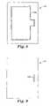
- FIG. 8is a top view of an upper die.
- FIG. 9is a top view of a lower die.
- the present inventionis described in terms of light directing films such as the 3M brand Brightness Enhancement Film, which has prism elements with apex angles of about 90°.
- light directing filmssuch as the 3M brand Brightness Enhancement Film, which has prism elements with apex angles of about 90°.
- any optical films for use in optical displaysinclude, for example, turning films, reflective polarizers including multilayer optical films, etc., as discussed previously.
- FIG. 1shows an optical display 10 , which includes case 12 , light source 14 , light directing film 16 , light gating device 18 , and cover sheet 20 .
- light directing film 16has a structured surface containing prism elements, which may be any of a variety of sizes and forms.
- the size of the structured surfacein particular, is greatly exaggerated for illustrative purposes.
- Sharp-tipped prism elements, such as shown hereare fragile and must be protected prior to assembly into optical display 10 .
- a protective cover, or pre-maskmust be applied to light directing film 16 and subsequently removed for installation.
- the followingis a description of a light directing product, which includes a protective cover laminated to a light directing film, as it comes to a manufacturer for assembly into an optical device and the method of making the product.
- FIGS. 2 and 3are top and cross-sectional side views, respectively, of a representative embodiment of the present invention.
- FIGS. 2 and 3show a light directing film for use in displays 22 , which includes light directing product with cover removal tab (tabbed product) 24 and liner 26 (shown cut away).
- Tabbed product 24further includes light directing product 28 ; tab 30 ; cut 32 , which divides light directing product 28 and tab 30 ; and protective covers 34 a and 34 b .
- FIG. 3which is a cross-section along section 3 — 3 of FIG. 2 , further shows that tabbed product 24 includes two layers, protective covers 34 a and 34 b and light directing films 36 a and 36 b .
- the perimeters, or edges, of protective covers 34 a and 34 b and light directing films 36 a and 36 bare the same shape and size so that when stacked the edges are aligned.
- Tab 30may be attached essentially anywhere along the perimeter of light directing product 28 .
- Tabbed product 24is manufactured on liner 26 and remains adhered to liner 26 until light directing film 36 a is assembled into an optical display. At this time, tabbed product 24 is detached from liner 26 . Typically, about 15 tabbed products 24 are adhered to a section of liner 26 , and when all of them are detached, liner 26 can be discarded.
- FIG. 4shows tabbed product 24 in use.
- protective covers 34 a and 34 b and light directing film 36 bmust be removed from light directing film 36 a .
- Tab 30which includes protective cover 34 b and light directing film 36 b , is pulled in a manner that peels protective cover 34 a from light directing film 36 a .
- Light directing film 36 ais now ready for installation.
- tabbed product 24is placed in the display prior to removing tab 30 and protective cover 34 a from light directing film 36 a.
- FIGS. 5 a – 5 fillustrate one method of making a light directing film for use in a display 22 .
- FIG. 5 ashows light directing film sheet 38 , which contains prism elements that can be made by any one of a variety of known techniques.
- protective cover sheet 40is laminated onto the structured surface of light directing film sheet 38 (see FIG. 1 ) to form web 42 .
- web 42is adhered to liner 26 forming web/liner 44 as shown in FIG. 5 c .
- the layering of sheets 38 and 40 and liner 26 to form web/liner 44can be performed in any order or done simultaneously.
- FIG. 5 ashows light directing film sheet 38 , which contains prism elements that can be made by any one of a variety of known techniques.
- protective cover sheet 40is laminated onto the structured surface of light directing film sheet 38 (see FIG. 1 ) to form web 42 .
- web 42is adhered to liner 26 forming web/liner 44 as shown in FIG. 5 c
- FIG. 5 dshows the positions of blade 46 a of upper die 46 and blade 48 a of lower die 48 relative to web/liner 44 .
- Upper and lower dies 46 and 48described in more detail below, cut web/liner 44 to form tabbed product 24 .
- blade 46 ais shown cutting down through web 42
- blade 48 ais shown cutting up through liner 26 and light directing film sheet 38 , although these cuts do not necessarily happen concurrently on a single tabbed product 24 .
- FIG. 5 fshows the resulting light directing film for use in displays 22 .
- FIG. 6illustrates a representative embodiment of a light directing film for use in a display with a transfer tape 50 .
- Transfer tape 52is adhered along the edges of light directing film 36 a opposite the structured surface, which is laminated to protective cover 34 a .
- Transfer tape 52is used to mount film 36 a on the back of a light guide in an optical display.
- FIG. 7shows a converting machine 54 that can be used with the present invention.
- FIG. 7includes converting machine 54 and web/liner 44 .
- Converting machine 54comprises unwinder 56 , stamping press 58 with upper die 46 and lower die 48 , stripper 60 , and sheet cutter 62 .
- rolls of web/liner 44are unwound by unwinder 56 and fed through stamping press 58 .
- Upper die 46 of stamping press 58vertically reciprocates, while lower die 48 of stamping press 58 is stationary.
- Upper die 46 and lower die 48cut web/liner 44 to form tabbed product 24 .
- Web/liner 44is then fed into stripper 60 where waste web 42 surrounding tabbed products 24 is stripped away.
- Web/liner 44is subsequently fed through sheet cutter 62 where liner 26 is cut into sections that carry one or more of tabbed products 24 .
- FIG. 8is an illustration of upper die 46 with blade 46 a . As shown, blade 46 a has the overall shape of tabbed product 24 . Upper die 46 reciprocates vertically to cut, or punch, out tabbed product 24 from web 42 .
- FIG. 9is an illustration of lower die 48 with blade 48 a .
- Blade 48 ais shaped to cut or sever at cut 32 .
- lower die 48is stationary and cuts through liner 26 to sever light directing film 36 a from light directing film 36 b ( FIGS. 2 and 3 ).
- dies 46 and 48cut concurrently, but more specifically by progressive cutting.
- die 48performs its cut for one tabbed product 24 .
- die 46performs its cut for a second tabbed product 24 that is actually positioned ahead of the first tabbed product 24 and was previously cut by die 48 .
- the cutscould alternatively be performed by sequential strokes, however, progressive cutting is the simplest and most efficient means of cutting.
- the present inventionhas several advantages. First, there is no imprint of tab 30 transferred to light directing film 36 a when tabbed products 24 are stacked or rolled-up for storage. Second, protective covers 34 a and 34 b are not larger than light directing films 36 a and 36 b , because having protective covers 34 a and 34 b larger than light directing films 36 a and 36 b is unacceptable to some users. Third, the method of making tabbed product 24 only requires a one punch-head converting machine. Fourth, there is minimal waste of material and time to add tab 30 . Fifth, the addition of tab 30 to light directing product 28 provides a way to easily remove a protective cover from a light directing film.
Landscapes
- Physics & Mathematics (AREA)
- General Physics & Mathematics (AREA)
- Optics & Photonics (AREA)
- Engineering & Computer Science (AREA)
- Health & Medical Sciences (AREA)
- Manufacturing & Machinery (AREA)
- Ophthalmology & Optometry (AREA)
- Mechanical Engineering (AREA)
- Polarising Elements (AREA)
- Optical Elements Other Than Lenses (AREA)
- Devices For Indicating Variable Information By Combining Individual Elements (AREA)
Abstract
Description
The present invention relates to optical films. In particular, the present invention relates to a tab, which allows easy removal of protective coverings from optical films and a method of forming the tab.
Optical films are used to increase the amount of light exiting an optical display in a preferred direction, typically this is a direction normal, or “on-axis,” to the surface of the display. Increasing the amount of on-axis light reduces the amount of energy required to generate a desired amount of on-axis luminance. This is particularly important for optical displays that use battery powered light sources such as those used in laptop computers, calculators, digital wristwatches, cellular phones, and personal digital assistants.
The 3M brand Brightness Enhancement Film from 3M Company, the assignee of the present invention, is used to address this problem. The film collects light from “off-axis” and redirects or “recycles” this light on-axis toward the viewer. In use, this material increases the on-axis luminance at the expense of off-axis luminance.
A “turning” film is also used to increase the amount of on-axis light exiting a display. Turning films are usually used in combination with wedge-shaped or stepped-wedge light guides. Light rays exiting the light guide at the glancing angle, usually less than 30° to the output surface, are internally reflected such that they are directed substantially on-axis. Representative embodiments of turning films are described in U.S. Pat. Nos. RE38,243 E and 4,984,144, which are assigned to 3M Company.
Another film used to increase on-axis light exiting a display is a reflective polarizer, these include multilayer optical films such as DBEF from 3M Company. The film is formed of layers of polymer that provides high polarized reflectivity over a wide bandwidth. Representative embodiments are described in U.S. Pat. No. 6,613,421, which is assigned to 3M Company.
Other examples of useful optical films manufactured by 3M Company are described in U.S. Pat. Nos. 5,828,488 and 4,906,070. These include films that are combinations of or variations of the films discussed above.
The films described above need to be protected. To prevent scratching or other damage prior to assembly in an optical display, a protective cover, or pre-mask, is laminated to the film.
Current products that include a film/pre-mask combination are manufactured by first laminating a sheet of pre-mask to a sheet of film and subsequently cutting the sheet of film/pre-mask with a single die to form the products. Because the pre-mask is the exact size of the film, and the edges of the film and the pre-mask are exactly aligned, removing the pre-mask during assembly of the display is difficult and time consuming.
The present invention is an optical product with a cover removal tab and a method of making the product. A web, comprised of a protective cover sheet and an optical film sheet, is cut to form the optical product with the cover removal tab. Another cut is through essentially only the optical film to divide the optical film and the cover removal tab so that the cover removal tab remains connected to the optical product by the protective cover.
The present invention is described in terms of light directing films such as the 3M brand Brightness Enhancement Film, which has prism elements with apex angles of about 90°. However, those skilled in the art know that it can be used with any optical films for use in optical displays. These include, for example, turning films, reflective polarizers including multilayer optical films, etc., as discussed previously.
Tabbedproduct 24 is manufactured onliner 26 and remains adhered toliner 26 until light directingfilm 36ais assembled into an optical display. At this time, tabbedproduct 24 is detached fromliner 26. Typically, about 15tabbed products 24 are adhered to a section ofliner 26, and when all of them are detached,liner 26 can be discarded.
Other layers may be added depending on the application and type of the film.FIG. 6 illustrates a representative embodiment of a light directing film for use in a display with atransfer tape 50.Transfer tape 52 is adhered along the edges oflight directing film 36aopposite the structured surface, which is laminated toprotective cover 34a.Transfer tape 52 is used to mountfilm 36aon the back of a light guide in an optical display.
In operation, rolls of web/liner 44 are unwound byunwinder 56 and fed through stampingpress 58. Upper die46 of stampingpress 58 vertically reciprocates, while lower die48 of stampingpress 58 is stationary. Upper die46 andlower die 48 cut web/liner 44 to form tabbedproduct 24. Web/liner 44 is then fed intostripper 60 wherewaste web 42 surrounding tabbedproducts 24 is stripped away. Web/liner 44 is subsequently fed throughsheet cutter 62 whereliner 26 is cut into sections that carry one or more of tabbedproducts 24.
Preferably, dies46 and48 cut concurrently, but more specifically by progressive cutting. During one stroke of stampingpress 58, die48 performs its cut for one tabbedproduct 24. At the same time, die46 performs its cut for a secondtabbed product 24 that is actually positioned ahead of the firsttabbed product 24 and was previously cut bydie 48. The cuts could alternatively be performed by sequential strokes, however, progressive cutting is the simplest and most efficient means of cutting.
Although the present invention has been discussed using a stamping process to form the cover removal tab for light directing products, it is well within the scope of this invention to use any means of converting a tab on light directing products. For example, a rotary converting process may also be used to form the cover removal tab.
The present invention has several advantages. First, there is no imprint oftab 30 transferred tolight directing film 36awhen tabbedproducts 24 are stacked or rolled-up for storage. Second,protective covers films protective covers films product 24 only requires a one punch-head converting machine. Fourth, there is minimal waste of material and time to addtab 30. Fifth, the addition oftab 30 to light directingproduct 28 provides a way to easily remove a protective cover from a light directing film.
Claims (23)
1. A method of making an optical product, the method comprising:
providing an optical film sheet having a first surface and a second surface, the first surface having an array of prism elements;
laminating a protective cover sheet to the first surface of the optical film sheet to form a web;
cutting the web to form the optical product, comprised of an optical film and a protective cover, with a cover removal tab; and
cutting essentially only the optical film sheet of the web between the optical product and the cover removal tab so that the cover removal tab remains connected to the optical product by the protective cover.
2. The method ofclaim 1 and further comprising:
laminating a transfer tape to the second surface of the optical film sheet; and
wherein the transfer tape is cut concurrently with the web.
3. The method ofclaim 1 wherein the web is carried by a liner that is cut concurrently with essentially only the optical film sheet of the web.
4. The method ofclaim 1 wherein the optical film is a turning film.
5. The method ofclaim 1 wherein the optical film is a multilayer optical film.
6. The method ofclaim 1 wherein the optical film is a light directing film.
7. A method of making an optical product, the method comprising:
cutting essentially only an optical film sheet of a web comprised of the optical film sheet and a protective cover sheet with a first die shaped to divide an optical film and a removal tab; and
cutting the web with a second die having a shape of the optical film with the removal tab.
8. The method ofclaim 7 wherein the first die and the second die cut in opposite directions.
9. The method ofclaim 7 and further comprising:
attaching the web to a liner.
10. A method of making an optical product, the method comprising:
laminating a protective cover sheet to an optical film sheet to form a web;
severing the web to form the optical product, comprised of a protective cover and an optical film, with a removal tab; and
severing, between the optical product and the removal tab, the optical film so that the removal tab remains connected to the optical product by the protective cover.
11. The method ofclaim 10 wherein removing the removal tab from the optical product also removes the protective cover from the optical film.
12. The method ofclaim 10 wherein the optical film is a light directing film having prism elements that have apex angles of about 90°.
13. The method ofclaim 10 wherein the optical film is a turning film.
14. The method ofclaim 10 wherein the optical film is a multilayer optical film.
15. An optical product with a removal tab comprising:
a protective cover stacked on an optical film, the protective cover being continuous between the optical product and the removal tab, the optical film being discontinuous between the optical product and the removal tab such that the removal tab is connected to the optical product by the protective cover.
16. The optical product with a removal tab ofclaim 15 and further comprising:
a transfer tape stacked underneath the optical film.
17. The optical product with a removal tab ofclaim 15 wherein the protective cover and the optical film have perimeters of equal size and shape, the perimeters being aligned.
18. The optical product with a removal tab ofclaim 15 wherein the optical film is a light directing film with prism elements having apex angles of about 90°.
19. The optical product with a removal tab ofclaim 15 wherein the optical film is a turning film.
20. The optical product with a removal tab ofclaim 15 wherein the optical film is a multilayer optical film.
21. An optical product with a removal tab comprising:
an optical product comprised of a layer of protective cover stacked on a layer of optical film, the layers having aligned edges;
a tab comprised of the layers and attached to an edge of the product such that the layer of protective cover is continuous between the product and the tab; and
a cut in the layer of optical film, the cut dividing the product and the tab such that the optical film is discontinuous between the product and the tab.
22. The optical product with a removal tab ofclaim 21 wherein the optical product is shaped for use in an optical display.
23. The optical product with a removal tab ofclaim 21 wherein the tab and the layer of protective cover of the optical product are removable from the layer of optical film of the product.
Priority Applications (7)
| Application Number | Priority Date | Filing Date | Title |
|---|---|---|---|
| US10/750,553US7147358B2 (en) | 2003-12-31 | 2003-12-31 | Cover removal tab for optical products |
| PCT/US2004/042554WO2005065922A1 (en) | 2003-12-31 | 2004-12-17 | A cover removal tab for optical products |
| JP2006547178AJP2007518597A (en) | 2003-12-31 | 2004-12-17 | Cover removal tab for optical products |
| KR1020067012993AKR20060101785A (en) | 2003-12-31 | 2004-12-17 | Cover Removal Tab for Optics |
| EP04814703AEP1699618A1 (en) | 2003-12-31 | 2004-12-17 | A cover removal tab for optical products |
| CNA2004800393950ACN1929987A (en) | 2003-12-31 | 2004-12-17 | Cover removal tab for optical products |
| TW093141410ATW200530631A (en) | 2003-12-31 | 2004-12-30 | A cover removal tab for optical products |
Applications Claiming Priority (1)
| Application Number | Priority Date | Filing Date | Title |
|---|---|---|---|
| US10/750,553US7147358B2 (en) | 2003-12-31 | 2003-12-31 | Cover removal tab for optical products |
Publications (2)
| Publication Number | Publication Date |
|---|---|
| US20050146881A1 US20050146881A1 (en) | 2005-07-07 |
| US7147358B2true US7147358B2 (en) | 2006-12-12 |
Family
ID=34711295
Family Applications (1)
| Application Number | Title | Priority Date | Filing Date |
|---|---|---|---|
| US10/750,553Expired - Fee RelatedUS7147358B2 (en) | 2003-12-31 | 2003-12-31 | Cover removal tab for optical products |
Country Status (7)
| Country | Link |
|---|---|
| US (1) | US7147358B2 (en) |
| EP (1) | EP1699618A1 (en) |
| JP (1) | JP2007518597A (en) |
| KR (1) | KR20060101785A (en) |
| CN (1) | CN1929987A (en) |
| TW (1) | TW200530631A (en) |
| WO (1) | WO2005065922A1 (en) |
Cited By (3)
| Publication number | Priority date | Publication date | Assignee | Title |
|---|---|---|---|---|
| US20060158592A1 (en)* | 2005-01-14 | 2006-07-20 | Freking Anthony J | Pre-stacked optical films |
| US20080101759A1 (en)* | 2006-10-26 | 2008-05-01 | K Laser Technology, Inc. | Prism matrix with random phase structures |
| US20080266501A1 (en)* | 2003-08-29 | 2008-10-30 | 3M Innovative Properties Company | Adhesive stacking for multiple optical films |
Families Citing this family (7)
| Publication number | Priority date | Publication date | Assignee | Title |
|---|---|---|---|---|
| JP2005347081A (en)* | 2004-06-02 | 2005-12-15 | Toyota Industries Corp | Surface light source device |
| WO2011039702A1 (en)* | 2009-10-01 | 2011-04-07 | Ehud Sarig | Manufacture of large sign backings |
| WO2015002685A1 (en)* | 2013-07-01 | 2015-01-08 | 3M Innovative Properties Company | Protection film suitable for illuminated display devices |
| KR101490760B1 (en)* | 2013-07-04 | 2015-02-11 | 에스케이씨 주식회사 | Cut-out laminated sheet and preparation method thereof |
| US9522511B2 (en) | 2013-07-04 | 2016-12-20 | Skc Co., Ltd | Cut-out laminated sheet and preparation method thereof |
| CN104119815B (en)* | 2014-08-04 | 2015-08-19 | 博洛尼家居用品(北京)股份有限公司 | A kind of double sticky tape |
| KR101692344B1 (en)* | 2015-07-29 | 2017-01-04 | (주)세경하이테크 | protection film production method |
Citations (79)
| Publication number | Priority date | Publication date | Assignee | Title |
|---|---|---|---|---|
| US3754813A (en) | 1971-12-13 | 1973-08-28 | Eastman Kodak Co | Radiation-redistributive devices |
| US3765281A (en) | 1971-12-13 | 1973-10-16 | Eastman Kodak Co | Method and apparatus for fabricating radiation-redistributive devices |
| US3788171A (en) | 1971-12-13 | 1974-01-29 | Eastman Kodak Co | Projection screen fabrication apparatus and method |
| US3851093A (en) | 1971-07-12 | 1974-11-26 | D Sunstein | Color television display system and method for reducing visibility of geometric pattern of colored-light sources, and method for fabrication thereof |
| USRE29091E (en) | 1971-12-13 | 1976-12-28 | Eastman Kodak Company | Radiation-redistributive devices |
| DE3407431A1 (en) | 1984-02-29 | 1985-08-29 | Siemens AG, 1000 Berlin und 8000 München | Lens for signal lights, in particular for traffic lights |
| US4542449A (en) | 1983-08-29 | 1985-09-17 | Canadian Patents & Development Limited | Lighting panel with opposed 45° corrugations |
| US4576850A (en)* | 1978-07-20 | 1986-03-18 | Minnesota Mining And Manufacturing Company | Shaped plastic articles having replicated microstructure surfaces |
| US4791540A (en) | 1987-05-26 | 1988-12-13 | Minnesota Mining And Manufacturing Company | Light fixture providing normalized output |
| US4804253A (en) | 1986-05-15 | 1989-02-14 | General Electric Company | Lenticular filter for display devices |
| US4906070A (en) | 1985-11-21 | 1990-03-06 | Minnesota Mining And Manufacturing Company | Totally internally reflecting thin, flexible film |
| EP0395957A1 (en) | 1989-04-21 | 1990-11-07 | Idemitsu Kosan Company Limited | Method of producing a substrate coated with a film of liquid crystal material and method and apparatus of producing a liquid crystal optical device |
| US4971719A (en) | 1989-09-22 | 1990-11-20 | General Motors Corporation | Polymer dispersed liquid crystal films formed by electron beam curing |
| US4984144A (en) | 1987-05-08 | 1991-01-08 | Minnesota Mining And Manufacturing Company | High aspect ratio light fixture and film for use therein |
| US5005108A (en) | 1989-02-10 | 1991-04-02 | Lumitex, Inc. | Thin panel illuminator |
| US5076668A (en) | 1988-01-25 | 1991-12-31 | Taliq Corporation | Gain reflector-liquid crystal display |
| US5128783A (en) | 1990-01-31 | 1992-07-07 | Ois Optical Imaging Systems, Inc. | Diffusing/collimating lens array for a liquid crystal display |
| US5146415A (en) | 1991-02-15 | 1992-09-08 | Faris Sades M | Self-aligned stereo printer |
| US5161041A (en) | 1990-04-26 | 1992-11-03 | Ois Optical Imaging Systems, Inc. | Lighting assembly for a backlit electronic display including an integral image splitting and collimating means |
| US5190370A (en) | 1991-08-21 | 1993-03-02 | Minnesota Mining And Manufacturing Company | High aspect ratio lighting element |
| EP0531939A1 (en) | 1991-09-09 | 1993-03-17 | Enplas Corporation | Surface light source device |
| US5247390A (en) | 1991-11-05 | 1993-09-21 | Aharon Zeev Hed | Lightweight low-loss refractive light diffusion system |
| US5268782A (en) | 1992-01-16 | 1993-12-07 | Minnesota Mining And Manufacturing Company | Micro-ridged, polymeric liquid crystal display substrate and display device |
| US5280371A (en) | 1992-07-09 | 1994-01-18 | Honeywell Inc. | Directional diffuser for a liquid crystal display |
| JPH0618707A (en) | 1992-06-30 | 1994-01-28 | Dainippon Printing Co Ltd | Lenticular lens, surface light source and liquid crystal display device |
| JPH06342106A (en) | 1992-07-31 | 1994-12-13 | Nissha Printing Co Ltd | Production of surface light emitting device |
| US5394255A (en) | 1992-01-27 | 1995-02-28 | Sekisui Kagaku Kogyo Kabushiki Kaisha | Liquid crystal display using a plurality of light adjusting sheets angled at 5 degrees or more |
| JPH0778254A (en) | 1993-09-08 | 1995-03-20 | Hitachi Ltd | Figure closed area extraction method |
| US5435963A (en) | 1991-09-09 | 1995-07-25 | Rackovan; Mitchell J. | In-mold labelling a coextruded, stretched and annealed label |
| US5467208A (en) | 1992-06-01 | 1995-11-14 | Sharp Kabushiki Kaisha | Liquid crystal display |
| US5492590A (en) | 1993-02-15 | 1996-02-20 | Matsushita Electric Industrial Co., Ltd. | Method for peeling the interlayer of a two-sided adhesive tape |
| US5521797A (en) | 1993-02-01 | 1996-05-28 | Tosoh Corporation | Backlighting device |
| US5550657A (en) | 1992-09-14 | 1996-08-27 | Fujitsu Limited | Liquid crystal display device having an optimized ridged layer to improve luminosity |
| US5552907A (en) | 1992-01-27 | 1996-09-03 | Sekisui Chemical Co., Ltd. | Light adjusting sheet having a sinusoidal surface and a non-optically flat surface and useable with an LCD |
| WO1996027757A1 (en) | 1995-03-03 | 1996-09-12 | Minnesota Mining And Manufacturing Company | Light directing film having variable height structured surface and light directing article constructed therefrom |
| US5592332A (en) | 1992-12-25 | 1997-01-07 | Dai Nippon Printing Co., Ltd. | Renticular lens, surface light source, and liquid crystal display apparatus |
| US5598280A (en) | 1993-03-23 | 1997-01-28 | Dai Nippon Printing Co., Ltd. | Film lens and a surface light source using the same |
| US5600462A (en) | 1992-09-16 | 1997-02-04 | International Business Machines Corporation | Optical film and liquid crystal display device using the film |
| US5600455A (en) | 1994-08-31 | 1997-02-04 | Enplas Corporation | Prismatic member with coarsened portions or triangular prismatic and semi-circular prismatic members arranged on a flat light emitting surface |
| EP0770899A1 (en) | 1995-10-24 | 1997-05-02 | AT&T Corp. | Composite for plastic liquid crystal display |
| US5627926A (en) | 1992-09-16 | 1997-05-06 | Hitachi, Ltd. | Prism plate for efficiently emitting light flux within a predetermined range, and liquid crystal indicator and indicator illumination method using the same |
| WO1997028468A1 (en) | 1996-02-05 | 1997-08-07 | Minnesota Mining And Manufacturing Company | Brightness enhancement film with soft cutoff |
| US5659408A (en) | 1995-05-24 | 1997-08-19 | Polaroid Corporation | Reflective image-providing display viewed with holographically diffused ambient light |
| JPH09267424A (en) | 1996-04-02 | 1997-10-14 | Nitto Denko Corp | Sheet member for surface light source device |
| US5828488A (en) | 1993-12-21 | 1998-10-27 | Minnesota Mining And Manufacturing Co. | Reflective polarizer display |
| US5919551A (en) | 1996-04-12 | 1999-07-06 | 3M Innovative Properties Company | Variable pitch structured optical film |
| JPH11259021A (en) | 1998-02-17 | 1999-09-24 | Internatl Business Mach Corp <Ibm> | Liquid crystal display panel and liquid crystal display device |
| US5997964A (en) | 1991-04-11 | 1999-12-07 | Sprayex Llc | Liquid crystal display |
| US6052164A (en) | 1993-03-01 | 2000-04-18 | 3M Innovative Properties Company | Electroluminescent display with brightness enhancement |
| US6079840A (en) | 1996-10-17 | 2000-06-27 | Enplas Corporation | Surface light source device having shielding layer |
| US6104854A (en) | 1996-03-29 | 2000-08-15 | Enplas Corporation | Light regulator and surface light source device |
| US6185043B1 (en) | 1998-01-14 | 2001-02-06 | Olympus Optical Co., Ltd. | Optical system having diffractive optical element and image pickup apparatus having diffractive optical element |
| US6191833B1 (en) | 1998-12-24 | 2001-02-20 | Hitachi, Ltd. | Liquid crystal display device having reflection film between prism sheet and liquid crystal panel |
| WO2001050160A1 (en) | 1999-12-30 | 2001-07-12 | 3M Innovative Properties Company | Segmented retroreflective sheeting and methods of making and using same |
| EP1134068A2 (en) | 2000-03-16 | 2001-09-19 | Colorlink, Inc. | Method and apparatus for laminating stacks of polycarbonate films |
| JP2001301104A (en) | 2000-04-24 | 2001-10-30 | Techno Works:Kk | Display article protecting sheet |
| US6322236B1 (en) | 1999-02-09 | 2001-11-27 | 3M Innovative Properties Company | Optical film with defect-reducing surface and method for making same |
| EP1168282A1 (en) | 2000-06-20 | 2002-01-02 | 3M Innovative Properties Company | Label for affixing to a garment |
| WO2002021167A1 (en) | 2000-09-01 | 2002-03-14 | 3M Innovative Properties Company | Sheeting having an optical core laminated to a vinyl film, retroreflective articles, and methods |
| US6364497B1 (en) | 1999-03-24 | 2002-04-02 | L G Chemical Ltd. | Backlight system |
| US6411353B1 (en) | 1998-04-22 | 2002-06-25 | Hitachi, Ltd. | Liquid crystal display device with its upper and lower cases clamped by crimping portions thereof |
| US20020080598A1 (en) | 1999-02-23 | 2002-06-27 | Parker Jeffery R. | Transreflectors, transreflector systems and displays and methods of making transreflectors |
| EP1220014A2 (en) | 2000-12-21 | 2002-07-03 | Nitto Denko Corporation | Optical film and liquid-crystal display device |
| US20020124950A1 (en) | 1997-08-21 | 2002-09-12 | Walter Klima | Liquid crystal display |
| US6462794B1 (en) | 1998-10-14 | 2002-10-08 | Hitachi, Ltd. | Image forming unit, enlarging unit, optical parts, and image display apparatus having these components |
| JP2002304254A (en) | 2001-04-05 | 2002-10-18 | Ricoh Co Ltd | Protective material for touch panel |
| US20020196397A1 (en) | 2001-06-07 | 2002-12-26 | Nitto Denko Corporation | Laminated optical film, method for producing the same film and liquid-crystal display device using the same film |
| WO2003010569A2 (en) | 2001-07-23 | 2003-02-06 | 3M Innovative Properties Company | Optical filter |
| US20030063251A1 (en) | 2001-10-01 | 2003-04-03 | Fujitsu Display Technologies Corporation | Method and apparatus for fabricating liquid crystal display device |
| EP1302922A2 (en) | 2001-10-10 | 2003-04-16 | ELTEX Industriekennzeichnung GmbH | Label with protection laminate |
| WO2003042747A2 (en) | 2001-11-09 | 2003-05-22 | 3M Innovative Properties Company | Optical devices having reflective and transmissive modes for display |
| US20030133207A1 (en) | 2001-08-03 | 2003-07-17 | Kazuhiko Minami | Optical filter |
| JP2003207767A (en) | 2002-01-16 | 2003-07-25 | Toshiba Corp | Surface light source device |
| US6613421B2 (en) | 1993-12-21 | 2003-09-02 | 3M Innovative Properties Company | Optical film |
| USRE38243E1 (en) | 1987-11-12 | 2003-09-02 | Mitsubishi Rayon Co., Ltd. | Plane light source unit |
| US6661482B2 (en) | 2001-10-05 | 2003-12-09 | Nitto Denko Corporation | Polarizing element, optical element, and liquid crystal display |
| US6685795B1 (en)* | 2001-08-10 | 2004-02-03 | Adco Products, Inc. | Device and method of separating adhered layers |
| US20040141103A1 (en) | 2003-01-16 | 2004-07-22 | Kotchick Keith M. | Packaging and handling method for optical films |
| US20050046767A1 (en) | 2003-08-29 | 2005-03-03 | Freking Anthony J. | Adhesive stacking for multiple optical films |
Family Cites Families (5)
| Publication number | Priority date | Publication date | Assignee | Title |
|---|---|---|---|---|
| US46767A (en)* | 1865-03-14 | Improved method of coating glass with platinum | ||
| US80598A (en)* | 1868-08-04 | Falls | ||
| US196397A (en)* | 1877-10-23 | Improvement in plates for artificial teeth | ||
| US1013282A (en)* | 1911-06-26 | 1912-01-02 | Hugh Duncan | Vehicle-wheel. |
| US1411031A (en)* | 1921-02-07 | 1922-03-28 | Jackson Frank | Plug |
- 2003
- 2003-12-31USUS10/750,553patent/US7147358B2/ennot_activeExpired - Fee Related
- 2004
- 2004-12-17WOPCT/US2004/042554patent/WO2005065922A1/ennot_activeApplication Discontinuation
- 2004-12-17KRKR1020067012993Apatent/KR20060101785A/ennot_activeWithdrawn
- 2004-12-17JPJP2006547178Apatent/JP2007518597A/ennot_activeWithdrawn
- 2004-12-17CNCNA2004800393950Apatent/CN1929987A/enactivePending
- 2004-12-17EPEP04814703Apatent/EP1699618A1/ennot_activeWithdrawn
- 2004-12-30TWTW093141410Apatent/TW200530631A/enunknown
Patent Citations (84)
| Publication number | Priority date | Publication date | Assignee | Title |
|---|---|---|---|---|
| US3851093A (en) | 1971-07-12 | 1974-11-26 | D Sunstein | Color television display system and method for reducing visibility of geometric pattern of colored-light sources, and method for fabrication thereof |
| US3765281A (en) | 1971-12-13 | 1973-10-16 | Eastman Kodak Co | Method and apparatus for fabricating radiation-redistributive devices |
| US3788171A (en) | 1971-12-13 | 1974-01-29 | Eastman Kodak Co | Projection screen fabrication apparatus and method |
| USRE29091E (en) | 1971-12-13 | 1976-12-28 | Eastman Kodak Company | Radiation-redistributive devices |
| US3754813A (en) | 1971-12-13 | 1973-08-28 | Eastman Kodak Co | Radiation-redistributive devices |
| US4576850A (en)* | 1978-07-20 | 1986-03-18 | Minnesota Mining And Manufacturing Company | Shaped plastic articles having replicated microstructure surfaces |
| US4542449A (en) | 1983-08-29 | 1985-09-17 | Canadian Patents & Development Limited | Lighting panel with opposed 45° corrugations |
| DE3407431A1 (en) | 1984-02-29 | 1985-08-29 | Siemens AG, 1000 Berlin und 8000 München | Lens for signal lights, in particular for traffic lights |
| US4906070A (en) | 1985-11-21 | 1990-03-06 | Minnesota Mining And Manufacturing Company | Totally internally reflecting thin, flexible film |
| US4804253A (en) | 1986-05-15 | 1989-02-14 | General Electric Company | Lenticular filter for display devices |
| US4984144A (en) | 1987-05-08 | 1991-01-08 | Minnesota Mining And Manufacturing Company | High aspect ratio light fixture and film for use therein |
| US4791540A (en) | 1987-05-26 | 1988-12-13 | Minnesota Mining And Manufacturing Company | Light fixture providing normalized output |
| USRE38243E1 (en) | 1987-11-12 | 2003-09-02 | Mitsubishi Rayon Co., Ltd. | Plane light source unit |
| US5076668A (en) | 1988-01-25 | 1991-12-31 | Taliq Corporation | Gain reflector-liquid crystal display |
| US5005108A (en) | 1989-02-10 | 1991-04-02 | Lumitex, Inc. | Thin panel illuminator |
| EP0395957A1 (en) | 1989-04-21 | 1990-11-07 | Idemitsu Kosan Company Limited | Method of producing a substrate coated with a film of liquid crystal material and method and apparatus of producing a liquid crystal optical device |
| US4971719A (en) | 1989-09-22 | 1990-11-20 | General Motors Corporation | Polymer dispersed liquid crystal films formed by electron beam curing |
| US5128783A (en) | 1990-01-31 | 1992-07-07 | Ois Optical Imaging Systems, Inc. | Diffusing/collimating lens array for a liquid crystal display |
| US5161041A (en) | 1990-04-26 | 1992-11-03 | Ois Optical Imaging Systems, Inc. | Lighting assembly for a backlit electronic display including an integral image splitting and collimating means |
| US5146415A (en) | 1991-02-15 | 1992-09-08 | Faris Sades M | Self-aligned stereo printer |
| US5997964A (en) | 1991-04-11 | 1999-12-07 | Sprayex Llc | Liquid crystal display |
| US5190370A (en) | 1991-08-21 | 1993-03-02 | Minnesota Mining And Manufacturing Company | High aspect ratio lighting element |
| EP0531939A1 (en) | 1991-09-09 | 1993-03-17 | Enplas Corporation | Surface light source device |
| US5435963A (en) | 1991-09-09 | 1995-07-25 | Rackovan; Mitchell J. | In-mold labelling a coextruded, stretched and annealed label |
| US5247390A (en) | 1991-11-05 | 1993-09-21 | Aharon Zeev Hed | Lightweight low-loss refractive light diffusion system |
| US5268782A (en) | 1992-01-16 | 1993-12-07 | Minnesota Mining And Manufacturing Company | Micro-ridged, polymeric liquid crystal display substrate and display device |
| US5394255A (en) | 1992-01-27 | 1995-02-28 | Sekisui Kagaku Kogyo Kabushiki Kaisha | Liquid crystal display using a plurality of light adjusting sheets angled at 5 degrees or more |
| US5552907A (en) | 1992-01-27 | 1996-09-03 | Sekisui Chemical Co., Ltd. | Light adjusting sheet having a sinusoidal surface and a non-optically flat surface and useable with an LCD |
| US5596429A (en) | 1992-06-01 | 1997-01-21 | Sharp Kabushiki Kaisha | Liquid crystal display |
| US5467208A (en) | 1992-06-01 | 1995-11-14 | Sharp Kabushiki Kaisha | Liquid crystal display |
| JPH0618707A (en) | 1992-06-30 | 1994-01-28 | Dainippon Printing Co Ltd | Lenticular lens, surface light source and liquid crystal display device |
| US5280371A (en) | 1992-07-09 | 1994-01-18 | Honeywell Inc. | Directional diffuser for a liquid crystal display |
| JPH06342106A (en) | 1992-07-31 | 1994-12-13 | Nissha Printing Co Ltd | Production of surface light emitting device |
| US5550657A (en) | 1992-09-14 | 1996-08-27 | Fujitsu Limited | Liquid crystal display device having an optimized ridged layer to improve luminosity |
| US5627926A (en) | 1992-09-16 | 1997-05-06 | Hitachi, Ltd. | Prism plate for efficiently emitting light flux within a predetermined range, and liquid crystal indicator and indicator illumination method using the same |
| US5600462A (en) | 1992-09-16 | 1997-02-04 | International Business Machines Corporation | Optical film and liquid crystal display device using the film |
| US5592332A (en) | 1992-12-25 | 1997-01-07 | Dai Nippon Printing Co., Ltd. | Renticular lens, surface light source, and liquid crystal display apparatus |
| US5521797A (en) | 1993-02-01 | 1996-05-28 | Tosoh Corporation | Backlighting device |
| US5492590A (en) | 1993-02-15 | 1996-02-20 | Matsushita Electric Industrial Co., Ltd. | Method for peeling the interlayer of a two-sided adhesive tape |
| US6052164A (en) | 1993-03-01 | 2000-04-18 | 3M Innovative Properties Company | Electroluminescent display with brightness enhancement |
| US5598280A (en) | 1993-03-23 | 1997-01-28 | Dai Nippon Printing Co., Ltd. | Film lens and a surface light source using the same |
| JPH0778254A (en) | 1993-09-08 | 1995-03-20 | Hitachi Ltd | Figure closed area extraction method |
| US6613421B2 (en) | 1993-12-21 | 2003-09-02 | 3M Innovative Properties Company | Optical film |
| US5828488A (en) | 1993-12-21 | 1998-10-27 | Minnesota Mining And Manufacturing Co. | Reflective polarizer display |
| US5600455A (en) | 1994-08-31 | 1997-02-04 | Enplas Corporation | Prismatic member with coarsened portions or triangular prismatic and semi-circular prismatic members arranged on a flat light emitting surface |
| WO1996027757A1 (en) | 1995-03-03 | 1996-09-12 | Minnesota Mining And Manufacturing Company | Light directing film having variable height structured surface and light directing article constructed therefrom |
| US5771328A (en) | 1995-03-03 | 1998-06-23 | Minnesota Mining And Manufacturing Company | Light directing film having variable height structured surface and light directing article constructed therefrom |
| US5659408A (en) | 1995-05-24 | 1997-08-19 | Polaroid Corporation | Reflective image-providing display viewed with holographically diffused ambient light |
| US5767931A (en) | 1995-10-24 | 1998-06-16 | Lucent Technologies Inc. | Composite for plastic liquid crystal display |
| EP0770899A1 (en) | 1995-10-24 | 1997-05-02 | AT&T Corp. | Composite for plastic liquid crystal display |
| WO1997028468A1 (en) | 1996-02-05 | 1997-08-07 | Minnesota Mining And Manufacturing Company | Brightness enhancement film with soft cutoff |
| US6104854A (en) | 1996-03-29 | 2000-08-15 | Enplas Corporation | Light regulator and surface light source device |
| JPH09267424A (en) | 1996-04-02 | 1997-10-14 | Nitto Denko Corp | Sheet member for surface light source device |
| US5919551A (en) | 1996-04-12 | 1999-07-06 | 3M Innovative Properties Company | Variable pitch structured optical film |
| US6079840A (en) | 1996-10-17 | 2000-06-27 | Enplas Corporation | Surface light source device having shielding layer |
| US20020124950A1 (en) | 1997-08-21 | 2002-09-12 | Walter Klima | Liquid crystal display |
| US6185043B1 (en) | 1998-01-14 | 2001-02-06 | Olympus Optical Co., Ltd. | Optical system having diffractive optical element and image pickup apparatus having diffractive optical element |
| JPH11259021A (en) | 1998-02-17 | 1999-09-24 | Internatl Business Mach Corp <Ibm> | Liquid crystal display panel and liquid crystal display device |
| US6538709B1 (en) | 1998-02-17 | 2003-03-25 | International Business Machines Corporation | LCD panel including plurality of display panel parts wrapped around by a thin plastic film envelope with an opening |
| US6411353B1 (en) | 1998-04-22 | 2002-06-25 | Hitachi, Ltd. | Liquid crystal display device with its upper and lower cases clamped by crimping portions thereof |
| US6462794B1 (en) | 1998-10-14 | 2002-10-08 | Hitachi, Ltd. | Image forming unit, enlarging unit, optical parts, and image display apparatus having these components |
| US6191833B1 (en) | 1998-12-24 | 2001-02-20 | Hitachi, Ltd. | Liquid crystal display device having reflection film between prism sheet and liquid crystal panel |
| US6322236B1 (en) | 1999-02-09 | 2001-11-27 | 3M Innovative Properties Company | Optical film with defect-reducing surface and method for making same |
| US20020080598A1 (en) | 1999-02-23 | 2002-06-27 | Parker Jeffery R. | Transreflectors, transreflector systems and displays and methods of making transreflectors |
| US6364497B1 (en) | 1999-03-24 | 2002-04-02 | L G Chemical Ltd. | Backlight system |
| WO2001050160A1 (en) | 1999-12-30 | 2001-07-12 | 3M Innovative Properties Company | Segmented retroreflective sheeting and methods of making and using same |
| EP1134068A2 (en) | 2000-03-16 | 2001-09-19 | Colorlink, Inc. | Method and apparatus for laminating stacks of polycarbonate films |
| JP2001301104A (en) | 2000-04-24 | 2001-10-30 | Techno Works:Kk | Display article protecting sheet |
| EP1168282A1 (en) | 2000-06-20 | 2002-01-02 | 3M Innovative Properties Company | Label for affixing to a garment |
| WO2002021167A1 (en) | 2000-09-01 | 2002-03-14 | 3M Innovative Properties Company | Sheeting having an optical core laminated to a vinyl film, retroreflective articles, and methods |
| EP1220014A2 (en) | 2000-12-21 | 2002-07-03 | Nitto Denko Corporation | Optical film and liquid-crystal display device |
| JP2002304254A (en) | 2001-04-05 | 2002-10-18 | Ricoh Co Ltd | Protective material for touch panel |
| US6661487B2 (en) | 2001-06-07 | 2003-12-09 | Nitto Denko Corporation | Laminated optical film, method for producing the same film and liquid-crystal display device using the same film |
| US20020196397A1 (en) | 2001-06-07 | 2002-12-26 | Nitto Denko Corporation | Laminated optical film, method for producing the same film and liquid-crystal display device using the same film |
| WO2003010569A2 (en) | 2001-07-23 | 2003-02-06 | 3M Innovative Properties Company | Optical filter |
| US20030133207A1 (en) | 2001-08-03 | 2003-07-17 | Kazuhiko Minami | Optical filter |
| US6685795B1 (en)* | 2001-08-10 | 2004-02-03 | Adco Products, Inc. | Device and method of separating adhered layers |
| US20030063251A1 (en) | 2001-10-01 | 2003-04-03 | Fujitsu Display Technologies Corporation | Method and apparatus for fabricating liquid crystal display device |
| US6661482B2 (en) | 2001-10-05 | 2003-12-09 | Nitto Denko Corporation | Polarizing element, optical element, and liquid crystal display |
| EP1302922A2 (en) | 2001-10-10 | 2003-04-16 | ELTEX Industriekennzeichnung GmbH | Label with protection laminate |
| WO2003042747A2 (en) | 2001-11-09 | 2003-05-22 | 3M Innovative Properties Company | Optical devices having reflective and transmissive modes for display |
| JP2003207767A (en) | 2002-01-16 | 2003-07-25 | Toshiba Corp | Surface light source device |
| US20040141103A1 (en) | 2003-01-16 | 2004-07-22 | Kotchick Keith M. | Packaging and handling method for optical films |
| US20050046767A1 (en) | 2003-08-29 | 2005-03-03 | Freking Anthony J. | Adhesive stacking for multiple optical films |
Non-Patent Citations (3)
| Title |
|---|
| U.S. Appl. No. 10/830,733, Title Optical Products for Displays, Filed Apr. 23, 2004, Nakayama et al., No. of pages, 16 specifications, 3 drawings. |
| U.S. Appl. No. 11/036,521, Title: Pre-Stacked Optical Films, Filed Jan. 14, 2005, Freking et al., No. of pages: 13 specifications, 8 drawings. |
| US 2001/0013282, 08/2001, LaBelle et al. (withdrawn) |
Cited By (5)
| Publication number | Priority date | Publication date | Assignee | Title |
|---|---|---|---|---|
| US20080266501A1 (en)* | 2003-08-29 | 2008-10-30 | 3M Innovative Properties Company | Adhesive stacking for multiple optical films |
| US7520654B2 (en) | 2003-08-29 | 2009-04-21 | 3M Innovative Properties Company | Adhesive stacking for multiple optical films |
| US20060158592A1 (en)* | 2005-01-14 | 2006-07-20 | Freking Anthony J | Pre-stacked optical films |
| US7339635B2 (en) | 2005-01-14 | 2008-03-04 | 3M Innovative Properties Company | Pre-stacked optical films with adhesive layer |
| US20080101759A1 (en)* | 2006-10-26 | 2008-05-01 | K Laser Technology, Inc. | Prism matrix with random phase structures |
Also Published As
| Publication number | Publication date |
|---|---|
| JP2007518597A (en) | 2007-07-12 |
| US20050146881A1 (en) | 2005-07-07 |
| KR20060101785A (en) | 2006-09-26 |
| TW200530631A (en) | 2005-09-16 |
| WO2005065922A1 (en) | 2005-07-21 |
| EP1699618A1 (en) | 2006-09-13 |
| CN1929987A (en) | 2007-03-14 |
Similar Documents
| Publication | Publication Date | Title |
|---|---|---|
| US7147358B2 (en) | Cover removal tab for optical products | |
| US7520654B2 (en) | Adhesive stacking for multiple optical films | |
| CN106541449A (en) | A kind of cross cutting waste discharge apparatus with inside casing cutting part and cross cutting waste discharge method | |
| TW201118437A (en) | Method for manufacturing polarizing plate | |
| US20100314032A1 (en) | Method of producing optical film laminate | |
| CN105739181A (en) | Frame adhesive, frame adhesive manufacturing method and backlight module manufacturing method | |
| CN109822672A (en) | A kind of circulation cabling die-cutting process | |
| CN115103581B (en) | Panel shielding assembly for notebook computer and production process thereof | |
| WO2005108073A1 (en) | Optical products for displays | |
| CN101189650B (en) | Film cutting and peeling cutter and film cutting and peeling device | |
| JPH0618383Y2 (en) | Adhesive label sheet for semiconductor manufacturing process | |
| CN108546520A (en) | A kind of belt glue film and its application method | |
| CN208485835U (en) | A kind of belt glue film | |
| CN111534242A (en) | Single-sided adhesive die cutting assembly with bent handle part and production process thereof | |
| CN113025217A (en) | Double-sided tape molding method and double-sided tape | |
| JP2000214324A (en) | Optical film with adhesive layer | |
| JP2007518597A5 (en) | ||
| JP5052573B2 (en) | Film antenna manufacturing method | |
| CN215395663U (en) | Touch screen protection film cutting die | |
| JP3021645U (en) | Adhesive sheet for semiconductor manufacturing process | |
| CN114670284B (en) | A production system for double-sided tape die-cut parts | |
| JP2005126643A (en) | Double-sided self-adhesive tape, method for producing frame-shaped double-sided self-adhesive tape and method for forming adhesive zone on outer circumference of sheet | |
| KR20170090595A (en) | Producting Methode for film | |
| US20070154681A1 (en) | Optical film delivery unit | |
| JP3188841B2 (en) | Easy-to-remove and reusable label and its manufacturing method |
Legal Events
| Date | Code | Title | Description |
|---|---|---|---|
| AS | Assignment | Owner name:3M INNOVATIVE PROPERTIES COMPANY, MINNESOTA Free format text:ASSIGNMENT OF ASSIGNORS INTEREST;ASSIGNORS:FREKING, ANTHONY J.;LU, ASHOK;FEI, JOHN;REEL/FRAME:015533/0425;SIGNING DATES FROM 20040628 TO 20040629 | |
| FPAY | Fee payment | Year of fee payment:4 | |
| REMI | Maintenance fee reminder mailed | ||
| LAPS | Lapse for failure to pay maintenance fees | ||
| STCH | Information on status: patent discontinuation | Free format text:PATENT EXPIRED DUE TO NONPAYMENT OF MAINTENANCE FEES UNDER 37 CFR 1.362 | |
| FP | Lapsed due to failure to pay maintenance fee | Effective date:20141212 |