US7141486B1 - Shallow trench isolation structures comprising a graded doped sacrificial silicon dioxide material and a method for forming shallow trench isolation structures - Google Patents
Shallow trench isolation structures comprising a graded doped sacrificial silicon dioxide material and a method for forming shallow trench isolation structuresDownload PDFInfo
- Publication number
- US7141486B1 US7141486B1US11/153,893US15389305AUS7141486B1US 7141486 B1US7141486 B1US 7141486B1US 15389305 AUS15389305 AUS 15389305AUS 7141486 B1US7141486 B1US 7141486B1
- Authority
- US
- United States
- Prior art keywords
- forming
- sacrificial layer
- doped
- taper angle
- layer
- Prior art date
- Legal status (The legal status is an assumption and is not a legal conclusion. Google has not performed a legal analysis and makes no representation as to the accuracy of the status listed.)
- Expired - Fee Related
Links
- 238000002955isolationMethods0.000titleclaimsabstractdescription29
- 238000000034methodMethods0.000titleclaimsdescription68
- 239000000463materialSubstances0.000titleclaimsdescription16
- VYPSYNLAJGMNEJ-UHFFFAOYSA-NSilicium dioxideChemical compoundO=[Si]=OVYPSYNLAJGMNEJ-UHFFFAOYSA-N0.000titleabstractdescription94
- 235000012239silicon dioxideNutrition0.000titleabstractdescription47
- 239000000377silicon dioxideSubstances0.000titleabstractdescription47
- 239000000758substrateSubstances0.000claimsabstractdescription50
- 229910052581Si3N4Inorganic materials0.000claimsdescription33
- HQVNEWCFYHHQES-UHFFFAOYSA-Nsilicon nitrideChemical compoundN12[Si]34N5[Si]62N3[Si]51N64HQVNEWCFYHHQES-UHFFFAOYSA-N0.000claimsdescription33
- 239000002019doping agentSubstances0.000claimsdescription30
- ZOXJGFHDIHLPTG-UHFFFAOYSA-NBoronChemical compound[B]ZOXJGFHDIHLPTG-UHFFFAOYSA-N0.000claimsdescription13
- XUIMIQQOPSSXEZ-UHFFFAOYSA-NSiliconChemical compound[Si]XUIMIQQOPSSXEZ-UHFFFAOYSA-N0.000claimsdescription13
- 229910052796boronInorganic materials0.000claimsdescription13
- 238000005530etchingMethods0.000claimsdescription13
- BHEPBYXIRTUNPN-UHFFFAOYSA-Nhydridophosphorus(.) (triplet)Chemical compound[PH]BHEPBYXIRTUNPN-UHFFFAOYSA-N0.000claimsdescription13
- 229910052710siliconInorganic materials0.000claimsdescription13
- 239000010703siliconSubstances0.000claimsdescription13
- 239000011810insulating materialSubstances0.000claimsdescription8
- 229920002120photoresistant polymerPolymers0.000claimsdescription8
- 229910021420polycrystalline siliconInorganic materials0.000abstractdescription10
- 229920005591polysiliconPolymers0.000abstractdescription10
- 239000004065semiconductorSubstances0.000abstractdescription10
- 230000015572biosynthetic processEffects0.000abstractdescription7
- 230000008021depositionEffects0.000abstractdescription6
- 230000001747exhibiting effectEffects0.000abstract1
- 229960001866silicon dioxideDrugs0.000description44
- 230000008569processEffects0.000description26
- 238000000151depositionMethods0.000description8
- 238000005498polishingMethods0.000description6
- BOTDANWDWHJENH-UHFFFAOYSA-NTetraethyl orthosilicateChemical compoundCCO[Si](OCC)(OCC)OCCBOTDANWDWHJENH-UHFFFAOYSA-N0.000description5
- 239000007789gasSubstances0.000description4
- 239000005360phosphosilicate glassSubstances0.000description4
- DQWPFSLDHJDLRL-UHFFFAOYSA-Ntriethyl phosphateChemical compoundCCOP(=O)(OCC)OCCDQWPFSLDHJDLRL-UHFFFAOYSA-N0.000description4
- 230000008901benefitEffects0.000description3
- 239000005380borophosphosilicate glassSubstances0.000description3
- 239000007788liquidSubstances0.000description3
- 230000003647oxidationEffects0.000description3
- 238000007254oxidation reactionMethods0.000description3
- 230000003071parasitic effectEffects0.000description3
- 238000000623plasma-assisted chemical vapour depositionMethods0.000description3
- 239000000126substanceSubstances0.000description3
- KRHYYFGTRYWZRS-UHFFFAOYSA-NFluoraneChemical compoundFKRHYYFGTRYWZRS-UHFFFAOYSA-N0.000description2
- BLRPTPMANUNPDV-UHFFFAOYSA-NSilaneChemical compound[SiH4]BLRPTPMANUNPDV-UHFFFAOYSA-N0.000description2
- 230000008859changeEffects0.000description2
- 238000004140cleaningMethods0.000description2
- 239000000470constituentSubstances0.000description2
- 230000007423decreaseEffects0.000description2
- 238000005516engineering processMethods0.000description2
- 230000005669field effectEffects0.000description2
- 239000001307heliumSubstances0.000description2
- 229910052734heliumInorganic materials0.000description2
- SWQJXJOGLNCZEY-UHFFFAOYSA-Nhelium atomChemical compound[He]SWQJXJOGLNCZEY-UHFFFAOYSA-N0.000description2
- 238000004518low pressure chemical vapour depositionMethods0.000description2
- 229910044991metal oxideInorganic materials0.000description2
- 150000004706metal oxidesChemical class0.000description2
- 230000001590oxidative effectEffects0.000description2
- 238000001020plasma etchingMethods0.000description2
- 229910000077silaneInorganic materials0.000description2
- AJSTXXYNEIHPMD-UHFFFAOYSA-Ntriethyl borateChemical compoundCCOB(OCC)OCCAJSTXXYNEIHPMD-UHFFFAOYSA-N0.000description2
- CBENFWSGALASAD-UHFFFAOYSA-NOzoneChemical compound[O-][O+]=OCBENFWSGALASAD-UHFFFAOYSA-N0.000description1
- QVGXLLKOCUKJST-UHFFFAOYSA-Natomic oxygenChemical compound[O]QVGXLLKOCUKJST-UHFFFAOYSA-N0.000description1
- 230000004888barrier functionEffects0.000description1
- 238000010276constructionMethods0.000description1
- 239000000356contaminantSubstances0.000description1
- 230000000593degrading effectEffects0.000description1
- 230000000694effectsEffects0.000description1
- 239000011521glassSubstances0.000description1
- 239000007943implantSubstances0.000description1
- 238000011065in-situ storageMethods0.000description1
- 230000003993interactionEffects0.000description1
- 238000004519manufacturing processMethods0.000description1
- 230000000873masking effectEffects0.000description1
- 239000001301oxygenSubstances0.000description1
- 229910052760oxygenInorganic materials0.000description1
- 238000005268plasma chemical vapour depositionMethods0.000description1
- 230000009467reductionEffects0.000description1
- 230000004044responseEffects0.000description1
- 238000001039wet etchingMethods0.000description1
Images


Classifications
- H—ELECTRICITY
- H01—ELECTRIC ELEMENTS
- H01L—SEMICONDUCTOR DEVICES NOT COVERED BY CLASS H10
- H01L21/00—Processes or apparatus adapted for the manufacture or treatment of semiconductor or solid state devices or of parts thereof
- H01L21/70—Manufacture or treatment of devices consisting of a plurality of solid state components formed in or on a common substrate or of parts thereof; Manufacture of integrated circuit devices or of parts thereof
- H01L21/71—Manufacture of specific parts of devices defined in group H01L21/70
- H01L21/76—Making of isolation regions between components
- H01L21/762—Dielectric regions, e.g. EPIC dielectric isolation, LOCOS; Trench refilling techniques, SOI technology, use of channel stoppers
- H01L21/76224—Dielectric regions, e.g. EPIC dielectric isolation, LOCOS; Trench refilling techniques, SOI technology, use of channel stoppers using trench refilling with dielectric materials
- H01L21/76232—Dielectric regions, e.g. EPIC dielectric isolation, LOCOS; Trench refilling techniques, SOI technology, use of channel stoppers using trench refilling with dielectric materials of trenches having a shape other than rectangular or V-shape, e.g. rounded corners, oblique or rounded trench walls
Definitions
- the present inventionrelates generally to integrated circuits and more particularly to a method for forming a shallow trench isolation (STI) structure within an integrated circuit, wherein the shallow trench isolation structure comprises a graded doped silicon dioxide material, and further to a shallow trench isolation structure comprising graded doped silicon dioxide material.
- STIshallow trench isolation
- Integrated circuitstypically comprise a silicon substrate and semiconductor devices, such as transistors, formed from doped regions within the substrate.
- Interconnect structures disposed in parallel-like layers overlying the semiconductor substrateprovide electrical connection between doped regions to form electrical devices and circuits.
- a conventional interconnect systemcomprises a plurality of substantially vertical conductive vias or plugs interconnecting substantially horizontal conductive traces, with a dielectric layer disposed between two vertically adjacent horizontal conductive traces.
- a parasitic bipolar structurei.e., a p-n-p-n thyristor
- the thyristoris off under normal operating conditions, if the isolation between doped regions is not sufficient, under certain bias conditions the p-n-p regions can supply base current to the n-p-n regions, causing a large current leakage between adjacent MOSFETS that can latch-up the CMOS device.
- a thick oxide regionwhether formed according to a local oxidation of silicon (LOCOS) process or an STI process as described below, electrically isolates adjacent transistors and other devices to minimize current therebetween and reduce these parasitic effects.
- the local oxidation of silicon processforms recessed LOCOS isolation regions in a non-active area (also referred to as a field region) of the semiconductor substrate.
- LOCOS regionsare formed in an area between the p-channel and n-channel devices of a CMOS device.
- a layer of silicon nitrideis deposited over the substrate and patterned according to conventional masking and etching steps to form openings that expose underlying substrate silicon.
- the isolating LOCOS regionsare formed by oxidizing the exposed silicon through the openings. No oxidation occurs in the masked regions.
- An STI structurecomprises a dielectric-filled substrate trench that electrically isolates doped regions of active devices, including CMOS devices, MOSFETS and bipolar transistors.
- STIis an important technology for device sizes below about 0.25 microns, as the trenches consume a smaller surface area and exhibit a flatter upper surface topology than the LOCOS structures. Since the shallow trench isolation structure consumes less substrate surface than the LOCOS structure, more transistors per unit area can be fabricated in an integrated circuit employing STI isolation techniques.
- STI structuresalso provide superior isolation because sharp corners at the bottom of the STI trench form voltage barriers that tend to block leakage currents between adjacent doped regions. LOCOS regions generally present rounded corners and thus may permit some leakage current.
- STI trenchesare typically about 3000 Angstroms deep.
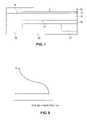
- FIGS. 1–6are cross-sectional views, not drawn to scale, illustrating successive prior art processing steps across a common plane for forming a shallow trench isolation structure in a substrate of one integrated circuit of the plurality of integrated circuits.
- a semiconductor substrate 30 in FIG. 1comprises active devices formed within doped regions depicted generally by a reference character 32 . It is desired to isolate these doped regions with a shallow trench isolation structure therebetween.
- a stress-reducing silicon dioxide layer 36(also referred to as a pad oxide layer 36 ) is deposited or grown over an upper surface 37 of the substrate 30 .
- a silicon nitride layer 38is deposited overlying the silicon dioxide layer 36 .
- the silicon nitride layer 38imposes stresses on the substrate 30 , with the stresses increasing with increasing thickness of the silicon nitride layer.
- the pad oxide layer 36isolates the substrate 30 from the silicon nitride layer 38 to reduce these stresses.
- a photoresist layer 40is deposited, exposed and developed according to known processes to form an opening 41 therein.
- an opening 46(see FIG. 2 ) is etched in the silicon nitride layer 38 , preferably using a plasma etching process. During the etching process, sidewalls 47 of the opening 46 are formed with a positive taper angle.
- the photoresist layer 40is removed and the wafer is cleaned.
- a trench 48is formed in the silicon dioxide layer 36 and the silicon substrate 30 during an etching step that uses the opening 46 as a mask.
- the positive taper angle in the sidewalls 47 of the opening 46creates a positive taper angle in sidewalls 49 of the trench 48 .
- a trench silicon dioxide liner 50is then formed or deposited in the trench 48 . See FIG. 4 .
- a shallow trench isolation (STI) structure 55is formed within the trench 48 according to a silicon dioxide deposition step (e.g., a high density plasma oxide deposition), during which silicon dioxide is also deposited on an upper surface 59 of the silicon nitride layer 38 .
- a chemical-mechanical polishing (CMP) stepremoves the silicon dioxide from the upper surface 59 , stopping on the silicon nitride layer 38 . Since the CMP polishing rate for silicon dioxide is different than the CMP polishing rate for silicon nitride, an upper surface 60 of the STI structure 55 is recessed below the upper surface 59 .
- FIG. 6illustrates the structural elements following these processing steps.
- the STI structureexhibits a re-entrant profile such that a top left comer 64 and a top right corner 66 together with sidewalls 67 and 68 define an oxide-undercut shape above the surface 37 .
- conventional cleaning steps following formation of the STI structure 55may cause additional undercutting in the sidewalls 67 and 68 , especially within notch regions 69 .
- the undercut profilesweaken the STI structure 55 .
- a gate polysilicon layeris deposited on the surface 37 .
- undesired polysilicon stringerscan form around the sidewalls 68 and 69 and the left and right comers 64 and 66 , creating short circuits that defeat the STI isolation function, thereby degrading performance of the integrated circuit.
- a process technology to avoid formation of the polysilicon stringersis highly desired.
- the oxide undercutby reducing a duration of the clean step (typically a hydrofluoric acid clean) that follows removal of the silicon nitride layer 38 and the pad oxide layer 36 .
- the shorter cleaning stepcauses material residues and contaminants to remain on the substrate, possibly causing undesirable short circuits or leakage current within the STI structure 55 and the substrate 30 .
- the present inventioncomprises a method for forming a shallow trench isolation structure in an integrated circuit.
- the methodcomprises providing a silicon substrate, forming a sacrificial layer having a graded doped concentration overlying the substrate, etching the sacrificial layer to form an opening therein, wherein sidewalls of the opening present a negative taper angle, etching the substrate in a region below the opening to form a trench therein and forming the shallow trench isolation structure by forming an insulating material in the opening and the trench, wherein the insulating material in the opening exhibits a negative taper angle.
- a semiconductor devicecomprises a substrate, a device isolation structure formed on the substrate, the device isolation structure further comprising a trench formed within the substrate and an insulating film filling the trench, the insulating film extending above an upper surface of the substrate and presenting a negative taper angle with respect to the substrate
- FIGS. 1–6are cross-sectional views of a substrate during successive processing steps to form a prior art shallow trench isolation structure.
- FIG. 7is a cross-sectional view of a substrate during a processing step to form a shallow trench isolation structure according to the teachings of the present invention.
- FIG. 8illustrates a doping profile for the graded doped silicon dioxide layer of the present invention.
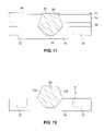
- FIGS. 9–12are cross-sectional views of a substrate during successive processing steps to form a shallow trench isolation structure according to the present invention.
- FIG. 13is a cross-sectional view of a substrate illustrating different sidewall profiles for the shallow trench isolation structure according to another embodiment of the present invention.
- the present inventioncomprises a technique for forming an STI structure having a negative taper angle above the substrate surface 37 , in contrast to the positive taper angle formed according to the prior art processes.
- a preferred methodology for forming the negative taper angleemploys a graded doped sacrificial silicon dioxide layer 70 (see FIG. 7 ) disposed (e.g., deposited) between a silicon nitride layer 71 and the pad silicon dioxide layer 36 .
- the negative taper angleincreases with increasing dopant concentration in the graded doped silicon dioxide layer 70 .
- the silicon nitride layer 71which functions as a CMP stop layer, is thinner according to the present invention than the silicon nitride layer 38 of the prior art process.
- the graded doped silicon dioxide layer 70comprises a layer about 1000 Angstroms thick comprising boron and phosphorous-doped oxide film (e.g., TEOS, plasma-deposited silane, LPCVD-deposited silane).
- the layer 70comprises a layer doped with either boron or phosphorous dopants.
- the graded doped oxide layer 70comprises a plurality of sublayers of different dopant concentrations and/or dopant types.
- the graded doped silicon dioxide layer 70can be doped in situ by introducing a gas or liquid containing the desired dopant into the atmosphere of the deposition chamber. Depending on the desired doping concentration, it may also be possible to dope the layer 70 using an implant doping process.
- the graded doped silicon dioxide layer 70 or one or more of the doped sublayers thereofcomprises a phosphoborosilicate glass (BPSG) material layer.
- the BPSG material layercan be formed by a low-pressure chemical vapor deposition (LPCVD) process, a plasma CVD process or a sub-atmospheric CVD (SACVD) process.
- LPCVDlow-pressure chemical vapor deposition
- SACVDsub-atmospheric CVD
- An exemplary SACVD process for depositing the BPSG material layeris performed at about 480 degrees C. and about 200 Torr.
- the constituent gas flow ratesare ozone (O 3 ) at about 4000 sccm and helium at about 6000 sccm.
- TEOStetraethyl orthosilicate
- TEBtriethylborate
- TEPOtriethylphosphate
- the graded doped silicon dioxide layer 70 or one or more of the doped sublayers thereofcomprises a phosphosilicate glass (PSG) material layer.
- the PSG material layercan be formed by a plasma-enhanced chemical vapor deposition (PECVD) process.
- PECVDplasma-enhanced chemical vapor deposition
- An exemplary PECVD process for depositing the PSG material layeris performed at about 480 degrees C. and about 2 Torr with 500 W applied to the plasma chamber.
- the constituent gas flow ratesare oxygen (O 2 ) at about 1400 sccm and helium at about 800 sccm.
- TEOStetraethyl orthosilicate
- TEPOtriethylphosphate
- a doping concentration of the graded doped silicon dioxide layer 70decreases from a first concentration (e.g., a maximum dopant concentration) at a surface 72 proximate the pad oxide layer 36 , to a second concentration, e.g., a minimum concentration, at a surface 76 proximate the silicon nitride layer 71 .
- a first concentratione.g., a maximum dopant concentration
- a second concentratione.g., a minimum concentration
- both the boron and phosphorous doping the concentrationsdecrease in a direction away from the surface 72 of the layer 70 , but the boron and phosphorous dopant concentrations may differ with respect to a slope of the doping concentration curve (the rate at which the doping concentration changes) and a magnitude of the doping concentration at any depth within the layer 70 . Both the rate of change of the concentration and the concentration magnitudes can be selected to achieve a desired etch profile for the STI structure. Also, in an embodiment wherein the graded doped silicon dioxide layer 70 comprises a plurality of sublayers, the shape of the doping profile may vary from the representative doping profile of FIG. 8 , as each sublayer may have a different doping concentration magnitude and slope as a function of layer depth.
- a phosphorous-doped silicon dioxide layeretches faster than a boron-doped silicon dioxide layer. Further, a phosphorous-doped plus boron-doped silicon-dioxide layer etches faster than a solely phosphorous-doped silicon dioxide layer.
- the STI etch rate and the STI sidewall profilecan be controlled by varying the relative dopant concentrations of phosphorous and boron, the rate at which the concentrations change, the concentration magnitudes within the layer 70 and the thickness of the layer 70 .
- the dopant concentrationranges from about 5% to about 1% for boron and about 5% to about 1% for phosphorous within the graded doped silicon dioxide layer 70 .
- a combined dopant concentration, i.e., boron plus phosphorous, of up to about 10%is permitted, but it may not be desirable for either concentration to exceed about 5%.
- a boron concentration of 3% plus a phosphorous concentration of 4%is acceptable, but a boron concentration of 3% plus a phosphorous concentration of 6% may not be desired since the phosphorous concentration exceeds 5%.
- the layer 70comprises a plurality of differently-doped sublayers having different doping concentrations (and in one embodiment different dopants) each sublayer exhibits a different etch rate, resulting in a different sidewall profile corresponding to each sublayer.
- the opening 46(see FIG. 9 ) with the sidewalls 47 is formed in the silicon nitride layer 71 .
- the photoresist layer 40is removed and using the opening 46 as an etch mask, an opening 80 having negative taper angle sidewalls 82 is formed in the graded doped silicon dioxide layer 70 and the pad oxide layer 36 , preferably using a wet etching process.
- the layer 70is etched using a plasma etching process.
- the sidewall profilesare substantially controlled by the doping of the layer 70 .
- an etch rate of a doped silicon dioxide materialis a direct function of the doping concentration, i.e., the etch rate increases with increasing doping concentration.
- the etch rateincreases with etch duration, forming the sidewalls 82 with a negative taper angle.
- a trench 88 having positive taper sidewalls 90is formed in the substrate 30 .
- the substrate etchis terminated after a predetermined etch duration or according to an etch endpoint technique.
- the silicon dioxide liner 50is then formed or deposited in the trench 88 .
- the liner 50is formed by oxidizing exposed silicon in the trench 88 to form a high quality silicon dioxide material layer.
- the pad silicon dioxide layer 36is not etched during etching of the graded doped silicon dioxide layer 70 . According to this embodiment the pad silicon dioxide layer 36 is etched during substrate etching.
- a shallow trench isolation structure 92is formed within the trench 88 according to a silicon dioxide deposition step during which silicon dioxide is deposited within the trench 80 and on an upper surface 94 of the silicon nitride layer 71 .
- a CMP stepremoves silicon dioxide from the upper surface 94 , stopping on the silicon nitride layer 71 . Since the CMP polishing rate for silicon dioxide is higher than the polishing rate for silicon nitride, an upper surface 95 of the STI structure 92 is recessed below the upper surface 94 .
- a distance “d”is about 100–300 Angstroms. Note sidewalls 100 of the STI structure 92 exhibit only a negative taper angle. No regions of positive taper angle or undercuts are present.
- the STI structure 92when formed in the trench 80 , the STI structure 92 may exhibit a slight positive taper angle in a region of the structure 92 adjacent the silicon nitride layer 71 . This region is removed by a combination of the CMP step that recesses the surface 95 below the surface 94 and the etching step that removes the silicon nitride layer 71 . Thus the final STI structure exhibits only a negative taper angle on the sidewalls 100 . In a plan view the STI structure exhibits a square or rectangular shape.
- the layer 71is removed prior to forming the STI silicon dioxide in the trench 80 , see FIG. 11 .
- the sidewalls 100do not exhibit any positive taper angle regions or undercuts.
- the STI structure 92 formed according to the teachings of the present inventiondoes not exhibit the disadvantageous re-entrant profiles and weak notch regions that are known to occur according to the prior art processes. Therefore, the STI structure 92 avoids the formation of polysilicon stringers and shorts when the polysilicon gate is formed later. By drastically reducing or eliminating the polysilicon shorts and leakage paths, fabrication processes employing the present invention enjoy a higher, more consistent yield and improved device performance.
- the dopant concentration during formation of the graded doped sacrificial silicon dioxide layer 70By controlling the dopant concentration during formation of the graded doped sacrificial silicon dioxide layer 70 , different sidewall profiles can be achieved. See for example, sidewalls 110 , 111 and 112 of FIG. 13 . Also, if the liner 50 is thicker than a conventional liner, then it may be advantageous to increase the sidewall taper angle by accordingly adjusting the dopant concentration.
- the silicon nitride layer 71preferably comprises a thinner material layer than the silicon nitride layer 38 of the prior art. According to the present invention, a thickness of the silicon nitride layer 71 can be reduced substantially from about 1600 Angstroms to about 500 to about 800 Angstroms since the graded doped silicon dioxide layer 70 can serve as a material stop layer for the chemical mechanical polishing step that removes silicon from the surface 94 .
- a thinner silicon nitride layerimposes less stress on the silicon substrate compared with the thicker silicon nitride layer that is required according to the prior art process. Improved wafer flatness, due to this stress reduction, results in better STI planarization.
Landscapes
- Engineering & Computer Science (AREA)
- Physics & Mathematics (AREA)
- Condensed Matter Physics & Semiconductors (AREA)
- General Physics & Mathematics (AREA)
- Manufacturing & Machinery (AREA)
- Computer Hardware Design (AREA)
- Microelectronics & Electronic Packaging (AREA)
- Power Engineering (AREA)
- Element Separation (AREA)
- Metal-Oxide And Bipolar Metal-Oxide Semiconductor Integrated Circuits (AREA)
Abstract
Description
Claims (25)
Priority Applications (1)
| Application Number | Priority Date | Filing Date | Title |
|---|---|---|---|
| US11/153,893US7141486B1 (en) | 2005-06-15 | 2005-06-15 | Shallow trench isolation structures comprising a graded doped sacrificial silicon dioxide material and a method for forming shallow trench isolation structures |
Applications Claiming Priority (1)
| Application Number | Priority Date | Filing Date | Title |
|---|---|---|---|
| US11/153,893US7141486B1 (en) | 2005-06-15 | 2005-06-15 | Shallow trench isolation structures comprising a graded doped sacrificial silicon dioxide material and a method for forming shallow trench isolation structures |
Publications (2)
| Publication Number | Publication Date |
|---|---|
| US7141486B1true US7141486B1 (en) | 2006-11-28 |
| US20060286739A1 US20060286739A1 (en) | 2006-12-21 |
Family
ID=37449887
Family Applications (1)
| Application Number | Title | Priority Date | Filing Date |
|---|---|---|---|
| US11/153,893Expired - Fee RelatedUS7141486B1 (en) | 2005-06-15 | 2005-06-15 | Shallow trench isolation structures comprising a graded doped sacrificial silicon dioxide material and a method for forming shallow trench isolation structures |
Country Status (1)
| Country | Link |
|---|---|
| US (1) | US7141486B1 (en) |
Cited By (8)
| Publication number | Priority date | Publication date | Assignee | Title |
|---|---|---|---|---|
| US20070063270A1 (en)* | 2005-09-22 | 2007-03-22 | Samsung Electronics Co., Ltd. | Transistors including laterally extended active regions and methods of fabricating the same |
| US20080157194A1 (en)* | 2006-03-22 | 2008-07-03 | Samsung Electronics Co., Ltd. | Transistors with laterally extended active regions and methods of fabricating same |
| KR100854502B1 (en)* | 2007-02-26 | 2008-08-26 | 삼성전자주식회사 | Semiconductor device adopting transistor having recess channel region and manufacturing method thereof |
| CN103151257A (en)* | 2013-03-14 | 2013-06-12 | 上海华力微电子有限公司 | Method for manufacturing sigma-shaped silicon grooves |
| US20150137309A1 (en)* | 2006-03-01 | 2015-05-21 | Infineon Technologies Ag | Methods of Fabricating Isolation Regions of Semiconductor Devices and Structures Thereof |
| US20150349055A1 (en)* | 2014-06-03 | 2015-12-03 | Renesas Electronics Corporation | Semiconductor device |
| US20160358810A1 (en)* | 2015-06-03 | 2016-12-08 | Macronix International Co., Ltd. | Semiconductor device and method of fabricating the same |
| US9613848B2 (en) | 2015-02-12 | 2017-04-04 | Infineon Technologies Ag | Dielectric structures with negative taper and methods of formation thereof |
Families Citing this family (6)
| Publication number | Priority date | Publication date | Assignee | Title |
|---|---|---|---|---|
| KR100745934B1 (en)* | 2006-06-30 | 2007-08-02 | 주식회사 하이닉스반도체 | Semiconductor element and formation method thereof |
| US8728891B2 (en) | 2010-09-21 | 2014-05-20 | Infineon Technologies Austria Ag | Method for producing contact openings in a semiconductor body and self-aligned contact structures on a semiconductor body |
| DE102010046213B3 (en) | 2010-09-21 | 2012-02-09 | Infineon Technologies Austria Ag | Method for producing a structural element and semiconductor component with a structural element |
| JP2014116707A (en)* | 2012-12-07 | 2014-06-26 | Seiko Epson Corp | Method of manufacturing vibrator |
| CN103311284B (en) | 2013-06-06 | 2015-11-25 | 苏州晶湛半导体有限公司 | Semiconductor device and preparation method thereof |
| CN111952360B (en)* | 2020-08-19 | 2023-02-21 | 深圳方正微电子有限公司 | Field Effect Transistor and Method for Making the Same |
Citations (15)
| Publication number | Priority date | Publication date | Assignee | Title |
|---|---|---|---|---|
| US3887404A (en)* | 1972-01-27 | 1975-06-03 | Philips Corp | Method of manufacturing semiconductor devices |
| US4341010A (en)* | 1979-04-24 | 1982-07-27 | U.S. Philips Corporation | Fabrication of electroluminescent semiconductor device utilizing selective etching and epitaxial deposition |
| US4571819A (en) | 1984-11-01 | 1986-02-25 | Ncr Corporation | Method for forming trench isolation structures |
| US5838055A (en) | 1997-05-29 | 1998-11-17 | International Business Machines Corporation | Trench sidewall patterned by vapor phase etching |
| US6235456B1 (en)* | 1998-12-09 | 2001-05-22 | Advanced Micros Devices, Inc. | Graded anti-reflective barrier films for ultra-fine lithography |
| US6355567B1 (en)* | 1999-06-30 | 2002-03-12 | International Business Machines Corporation | Retrograde openings in thin films |
| US20020037627A1 (en)* | 2000-08-10 | 2002-03-28 | Liu Mark Y. | Extension of shallow trench isolation by ion implantation |
| US20020055231A1 (en)* | 1998-05-08 | 2002-05-09 | Clampitt Darwin A. | Semiconductor structure having more usable substrate area and method for forming same |
| US20030003681A1 (en)* | 2001-06-30 | 2003-01-02 | Daniel Xu | Trench sidewall profile for device isolation |
| US6566226B2 (en) | 1998-12-25 | 2003-05-20 | Fujitsu Limited | Semiconductor device and fabrication process thereof, method of forming a device isolation structure |
| US6825544B1 (en) | 1998-12-09 | 2004-11-30 | Cypress Semiconductor Corporation | Method for shallow trench isolation and shallow trench isolation structure |
| US6828646B2 (en) | 2001-10-17 | 2004-12-07 | Stmicroelectronics Sa | Isolating trench and manufacturing process |
| US6849919B2 (en) | 2001-08-13 | 2005-02-01 | Renesas Technology Corp. | Method of fabricating a semiconductor device with a trench isolation structure and resulting semiconductor device |
| US20050085056A1 (en)* | 2003-10-17 | 2005-04-21 | Chartered Semiconductor Manufacturing Ltd. | Integrated circuit with protected implantation profiles and method for the formation thereof |
| US20050133828A1 (en)* | 2003-09-05 | 2005-06-23 | Chia-Shun Hsiao | Corner protection to reduce wrap around |
Family Cites Families (2)
| Publication number | Priority date | Publication date | Assignee | Title |
|---|---|---|---|---|
| US6945933B2 (en)* | 2002-06-26 | 2005-09-20 | Sdgi Holdings, Inc. | Instruments and methods for minimally invasive tissue retraction and surgery |
| US6869398B2 (en)* | 2003-01-06 | 2005-03-22 | Theodore G. Obenchain | Four-blade surgical speculum |
- 2005
- 2005-06-15USUS11/153,893patent/US7141486B1/ennot_activeExpired - Fee Related
Patent Citations (16)
| Publication number | Priority date | Publication date | Assignee | Title |
|---|---|---|---|---|
| US3887404A (en)* | 1972-01-27 | 1975-06-03 | Philips Corp | Method of manufacturing semiconductor devices |
| US4341010A (en)* | 1979-04-24 | 1982-07-27 | U.S. Philips Corporation | Fabrication of electroluminescent semiconductor device utilizing selective etching and epitaxial deposition |
| US4571819A (en) | 1984-11-01 | 1986-02-25 | Ncr Corporation | Method for forming trench isolation structures |
| US5838055A (en) | 1997-05-29 | 1998-11-17 | International Business Machines Corporation | Trench sidewall patterned by vapor phase etching |
| US20020055231A1 (en)* | 1998-05-08 | 2002-05-09 | Clampitt Darwin A. | Semiconductor structure having more usable substrate area and method for forming same |
| US6235456B1 (en)* | 1998-12-09 | 2001-05-22 | Advanced Micros Devices, Inc. | Graded anti-reflective barrier films for ultra-fine lithography |
| US6825544B1 (en) | 1998-12-09 | 2004-11-30 | Cypress Semiconductor Corporation | Method for shallow trench isolation and shallow trench isolation structure |
| US6566226B2 (en) | 1998-12-25 | 2003-05-20 | Fujitsu Limited | Semiconductor device and fabrication process thereof, method of forming a device isolation structure |
| US6355567B1 (en)* | 1999-06-30 | 2002-03-12 | International Business Machines Corporation | Retrograde openings in thin films |
| US20020037627A1 (en)* | 2000-08-10 | 2002-03-28 | Liu Mark Y. | Extension of shallow trench isolation by ion implantation |
| US20030003681A1 (en)* | 2001-06-30 | 2003-01-02 | Daniel Xu | Trench sidewall profile for device isolation |
| US6514805B2 (en)* | 2001-06-30 | 2003-02-04 | Intel Corporation | Trench sidewall profile for device isolation |
| US6849919B2 (en) | 2001-08-13 | 2005-02-01 | Renesas Technology Corp. | Method of fabricating a semiconductor device with a trench isolation structure and resulting semiconductor device |
| US6828646B2 (en) | 2001-10-17 | 2004-12-07 | Stmicroelectronics Sa | Isolating trench and manufacturing process |
| US20050133828A1 (en)* | 2003-09-05 | 2005-06-23 | Chia-Shun Hsiao | Corner protection to reduce wrap around |
| US20050085056A1 (en)* | 2003-10-17 | 2005-04-21 | Chartered Semiconductor Manufacturing Ltd. | Integrated circuit with protected implantation profiles and method for the formation thereof |
Cited By (15)
| Publication number | Priority date | Publication date | Assignee | Title |
|---|---|---|---|---|
| US20070063270A1 (en)* | 2005-09-22 | 2007-03-22 | Samsung Electronics Co., Ltd. | Transistors including laterally extended active regions and methods of fabricating the same |
| US7470588B2 (en) | 2005-09-22 | 2008-12-30 | Samsung Electronics Co., Ltd. | Transistors including laterally extended active regions and methods of fabricating the same |
| US9653543B2 (en)* | 2006-03-01 | 2017-05-16 | Infineon Technologies Ag | Methods of fabricating isolation regions of semiconductor devices and structures thereof |
| US20150137309A1 (en)* | 2006-03-01 | 2015-05-21 | Infineon Technologies Ag | Methods of Fabricating Isolation Regions of Semiconductor Devices and Structures Thereof |
| US8133786B2 (en) | 2006-03-22 | 2012-03-13 | Samsung Electronics Co., Ltd. | Transistors with laterally extended active regions and methods of fabricating same |
| US20110183482A1 (en)* | 2006-03-22 | 2011-07-28 | Samsung Electronics Co., Ltd. | Transistors with laterally extended active regions and methods of fabricating same |
| US7902597B2 (en) | 2006-03-22 | 2011-03-08 | Samsung Electronics Co., Ltd. | Transistors with laterally extended active regions and methods of fabricating same |
| US20080157194A1 (en)* | 2006-03-22 | 2008-07-03 | Samsung Electronics Co., Ltd. | Transistors with laterally extended active regions and methods of fabricating same |
| KR100854502B1 (en)* | 2007-02-26 | 2008-08-26 | 삼성전자주식회사 | Semiconductor device adopting transistor having recess channel region and manufacturing method thereof |
| CN103151257A (en)* | 2013-03-14 | 2013-06-12 | 上海华力微电子有限公司 | Method for manufacturing sigma-shaped silicon grooves |
| US20150349055A1 (en)* | 2014-06-03 | 2015-12-03 | Renesas Electronics Corporation | Semiconductor device |
| US9691852B2 (en)* | 2014-06-03 | 2017-06-27 | Renesas Electronics Corporation | Semiconductor device |
| US9613848B2 (en) | 2015-02-12 | 2017-04-04 | Infineon Technologies Ag | Dielectric structures with negative taper and methods of formation thereof |
| US20160358810A1 (en)* | 2015-06-03 | 2016-12-08 | Macronix International Co., Ltd. | Semiconductor device and method of fabricating the same |
| US9627247B2 (en)* | 2015-06-03 | 2017-04-18 | Macronix International Co., Ltd. | Semiconductor device and method of fabricating the same |
Also Published As
| Publication number | Publication date |
|---|---|
| US20060286739A1 (en) | 2006-12-21 |
Similar Documents
| Publication | Publication Date | Title |
|---|---|---|
| US7906407B2 (en) | Shallow trench isolation structures and a method for forming shallow trench isolation structures | |
| KR100470086B1 (en) | Semiconductor device and manufacturing method thereof | |
| US5817568A (en) | Method of forming a trench isolation region | |
| US6214698B1 (en) | Shallow trench isolation methods employing gap filling doped silicon oxide dielectric layer | |
| US7141486B1 (en) | Shallow trench isolation structures comprising a graded doped sacrificial silicon dioxide material and a method for forming shallow trench isolation structures | |
| US5811345A (en) | Planarization of shallow- trench- isolation without chemical mechanical polishing | |
| US8022481B2 (en) | Robust shallow trench isolation structures and a method for forming shallow trench isolation structures | |
| US20070190742A1 (en) | Semiconductor device including shallow trench isolator and method of forming same | |
| US6649489B1 (en) | Poly etching solution to improve silicon trench for low STI profile | |
| US6391729B1 (en) | Shallow trench isolation formation to eliminate poly stringer with controlled step height and corner rounding | |
| US20030003678A1 (en) | Method of forming shallow trench isolation for thin silicon-on-insulator substrates | |
| KR100518587B1 (en) | Fabrication Method for shallow trench isolation structure and microelectronic device having the same structure | |
| US6171929B1 (en) | Shallow trench isolator via non-critical chemical mechanical polishing | |
| US6248641B1 (en) | Method of fabricating shallow trench isolation | |
| KR20010024284A (en) | Method for making a groove structure with a silicium substrate | |
| US6602759B2 (en) | Shallow trench isolation for thin silicon/silicon-on-insulator substrates by utilizing polysilicon | |
| US20040038493A1 (en) | Method for forming a trench isolation structure | |
| US20070087565A1 (en) | Methods of forming isolation regions and structures thereof | |
| US6159821A (en) | Methods for shallow trench isolation | |
| US7026172B2 (en) | Reduced thickness variation in a material layer deposited in narrow and wide integrated circuit trenches | |
| CN1237602C (en) | Method for forming trench isolation structure | |
| US6187650B1 (en) | Method for improving global planarization uniformity of a silicon nitride layer used in the formation of trenches by using a sandwich stop layer | |
| US20010053583A1 (en) | Shallow trench isolation formation process using a sacrificial layer | |
| KR100455726B1 (en) | Method for forming isolation layer in semiconductor device | |
| KR20050012584A (en) | Method for forming isolation layer of semiconductor device |
Legal Events
| Date | Code | Title | Description |
|---|---|---|---|
| AS | Assignment | Owner name:AGERE SYSTEMS INC., PENNSYLVANIA Free format text:ASSIGNMENT OF ASSIGNORS INTEREST;ASSIGNORS:ROSSI, NACE;SINGH, RANBIR;NANDA, ARUN K.;REEL/FRAME:016534/0748;SIGNING DATES FROM 20050708 TO 20050712 | |
| FEPP | Fee payment procedure | Free format text:PAYOR NUMBER ASSIGNED (ORIGINAL EVENT CODE: ASPN); ENTITY STATUS OF PATENT OWNER: LARGE ENTITY | |
| FPAY | Fee payment | Year of fee payment:4 | |
| FPAY | Fee payment | Year of fee payment:8 | |
| AS | Assignment | Owner name:DEUTSCHE BANK AG NEW YORK BRANCH, AS COLLATERAL AG Free format text:PATENT SECURITY AGREEMENT;ASSIGNORS:LSI CORPORATION;AGERE SYSTEMS LLC;REEL/FRAME:032856/0031 Effective date:20140506 | |
| AS | Assignment | Owner name:AVAGO TECHNOLOGIES GENERAL IP (SINGAPORE) PTE. LTD Free format text:ASSIGNMENT OF ASSIGNORS INTEREST;ASSIGNOR:AGERE SYSTEMS LLC;REEL/FRAME:035365/0634 Effective date:20140804 | |
| AS | Assignment | Owner name:LSI CORPORATION, CALIFORNIA Free format text:TERMINATION AND RELEASE OF SECURITY INTEREST IN PATENT RIGHTS (RELEASES RF 032856-0031);ASSIGNOR:DEUTSCHE BANK AG NEW YORK BRANCH, AS COLLATERAL AGENT;REEL/FRAME:037684/0039 Effective date:20160201 Owner name:AGERE SYSTEMS LLC, PENNSYLVANIA Free format text:TERMINATION AND RELEASE OF SECURITY INTEREST IN PATENT RIGHTS (RELEASES RF 032856-0031);ASSIGNOR:DEUTSCHE BANK AG NEW YORK BRANCH, AS COLLATERAL AGENT;REEL/FRAME:037684/0039 Effective date:20160201 | |
| AS | Assignment | Owner name:BANK OF AMERICA, N.A., AS COLLATERAL AGENT, NORTH CAROLINA Free format text:PATENT SECURITY AGREEMENT;ASSIGNOR:AVAGO TECHNOLOGIES GENERAL IP (SINGAPORE) PTE. LTD.;REEL/FRAME:037808/0001 Effective date:20160201 Owner name:BANK OF AMERICA, N.A., AS COLLATERAL AGENT, NORTH Free format text:PATENT SECURITY AGREEMENT;ASSIGNOR:AVAGO TECHNOLOGIES GENERAL IP (SINGAPORE) PTE. LTD.;REEL/FRAME:037808/0001 Effective date:20160201 | |
| AS | Assignment | Owner name:AVAGO TECHNOLOGIES GENERAL IP (SINGAPORE) PTE. LTD., SINGAPORE Free format text:TERMINATION AND RELEASE OF SECURITY INTEREST IN PATENTS;ASSIGNOR:BANK OF AMERICA, N.A., AS COLLATERAL AGENT;REEL/FRAME:041710/0001 Effective date:20170119 Owner name:AVAGO TECHNOLOGIES GENERAL IP (SINGAPORE) PTE. LTD Free format text:TERMINATION AND RELEASE OF SECURITY INTEREST IN PATENTS;ASSIGNOR:BANK OF AMERICA, N.A., AS COLLATERAL AGENT;REEL/FRAME:041710/0001 Effective date:20170119 | |
| AS | Assignment | Owner name:BELL SEMICONDUCTOR, LLC, ILLINOIS Free format text:ASSIGNMENT OF ASSIGNORS INTEREST;ASSIGNORS:AVAGO TECHNOLOGIES GENERAL IP (SINGAPORE) PTE. LTD.;BROADCOM CORPORATION;REEL/FRAME:044886/0608 Effective date:20171208 | |
| AS | Assignment | Owner name:CORTLAND CAPITAL MARKET SERVICES LLC, AS COLLATERA Free format text:SECURITY INTEREST;ASSIGNORS:HILCO PATENT ACQUISITION 56, LLC;BELL SEMICONDUCTOR, LLC;BELL NORTHERN RESEARCH, LLC;REEL/FRAME:045216/0020 Effective date:20180124 | |
| FEPP | Fee payment procedure | Free format text:MAINTENANCE FEE REMINDER MAILED (ORIGINAL EVENT CODE: REM.) | |
| LAPS | Lapse for failure to pay maintenance fees | Free format text:PATENT EXPIRED FOR FAILURE TO PAY MAINTENANCE FEES (ORIGINAL EVENT CODE: EXP.); ENTITY STATUS OF PATENT OWNER: LARGE ENTITY | |
| STCH | Information on status: patent discontinuation | Free format text:PATENT EXPIRED DUE TO NONPAYMENT OF MAINTENANCE FEES UNDER 37 CFR 1.362 | |
| FP | Lapsed due to failure to pay maintenance fee | Effective date:20181128 | |
| AS | Assignment | Owner name:BELL NORTHERN RESEARCH, LLC, ILLINOIS Free format text:RELEASE BY SECURED PARTY;ASSIGNOR:CORTLAND CAPITAL MARKET SERVICES LLC;REEL/FRAME:059720/0719 Effective date:20220401 Owner name:BELL SEMICONDUCTOR, LLC, ILLINOIS Free format text:RELEASE BY SECURED PARTY;ASSIGNOR:CORTLAND CAPITAL MARKET SERVICES LLC;REEL/FRAME:059720/0719 Effective date:20220401 Owner name:HILCO PATENT ACQUISITION 56, LLC, ILLINOIS Free format text:RELEASE BY SECURED PARTY;ASSIGNOR:CORTLAND CAPITAL MARKET SERVICES LLC;REEL/FRAME:059720/0719 Effective date:20220401 |