US7139203B2 - Voltage regulator and data path for a memory device - Google Patents
Voltage regulator and data path for a memory deviceDownload PDFInfo
- Publication number
- US7139203B2 US7139203B2US10/678,595US67859503AUS7139203B2US 7139203 B2US7139203 B2US 7139203B2US 67859503 AUS67859503 AUS 67859503AUS 7139203 B2US7139203 B2US 7139203B2
- Authority
- US
- United States
- Prior art keywords
- output
- driver
- data path
- data
- pair
- Prior art date
- Legal status (The legal status is an assumption and is not a legal conclusion. Google has not performed a legal analysis and makes no representation as to the accuracy of the status listed.)
- Expired - Lifetime
Links
- 230000004044responseEffects0.000claimsabstractdescription14
- 238000000034methodMethods0.000claimsabstractdescription13
- 230000003321amplificationEffects0.000claimsabstract2
- 238000003199nucleic acid amplification methodMethods0.000claimsabstract2
- 230000003111delayed effectEffects0.000claimsdescription27
- 230000015654memoryEffects0.000claimsdescription13
- 230000011664signalingEffects0.000claims1
- 238000010586diagramMethods0.000description8
- 230000008859changeEffects0.000description6
- 230000008569processEffects0.000description3
- 239000004606Fillers/ExtendersSubstances0.000description2
- 230000008901benefitEffects0.000description2
- 230000003139buffering effectEffects0.000description2
- 239000003990capacitorSubstances0.000description2
- 230000006870functionEffects0.000description2
- 238000012986modificationMethods0.000description2
- 230000004048modificationEffects0.000description2
- 230000009467reductionEffects0.000description2
- 239000007787solidSubstances0.000description2
- 238000003860storageMethods0.000description2
- 230000033228biological regulationEffects0.000description1
- 238000004364calculation methodMethods0.000description1
- 238000013500data storageMethods0.000description1
- 230000003247decreasing effectEffects0.000description1
- 230000003292diminished effectEffects0.000description1
- 238000004519manufacturing processMethods0.000description1
- 230000001902propagating effectEffects0.000description1
- 238000011084recoveryMethods0.000description1
- 238000004513sizingMethods0.000description1
- 238000012358sourcingMethods0.000description1
- 230000003068static effectEffects0.000description1
- 230000001960triggered effectEffects0.000description1
Images


Classifications
- G—PHYSICS
- G11—INFORMATION STORAGE
- G11C—STATIC STORES
- G11C5/00—Details of stores covered by group G11C11/00
- G11C5/14—Power supply arrangements, e.g. power down, chip selection or deselection, layout of wirings or power grids, or multiple supply levels
- G11C5/147—Voltage reference generators, voltage or current regulators; Internally lowered supply levels; Compensation for voltage drops
- G—PHYSICS
- G11—INFORMATION STORAGE
- G11C—STATIC STORES
- G11C5/00—Details of stores covered by group G11C11/00
- G11C5/14—Power supply arrangements, e.g. power down, chip selection or deselection, layout of wirings or power grids, or multiple supply levels
- G11C5/145—Applications of charge pumps; Boosted voltage circuits; Clamp circuits therefor
Definitions
- the present inventionis directed to memory devices generally and, more particularly, to voltage regulators and data paths used in such devices.
- Solid state memory devicescommunicate with the outside world through input/output pads. Some pads may be connected to an address bus and are thus dedicated to receiving address information. Other pads may be connected to a command bus from which command signals are received while still other pads are connected to a data bus, on which data to be written into the memory is received or data read from the memory is output. In other types of devices, the pads may be connected to a single multiplexed bus which, at one point in time outputs address and command information and, at another point in time, outputs or receives data.
- the informationis transmitted in the form of ones and zeros.
- the “ones” and “zeros”are typically represented by two different voltage levels. For example, a voltage between two and five and one half volts may be considered to represent a high signal, or a “one”, while a voltage level of between minus 0.3 volts and plus 0.8 volts may be considered to represent a low signal, or a “zero”.
- the output padsmust be capable of reliably producing voltages within the ranges designated as representing ones and zeroes in accordance with timing specifications set for the component.
- Timing specificationsare typically set by the consumers of the memory devices for particular applications.
- a timing specificationwould identify how long it may take for an output pad to change from a zero to a one, e.g. change from minus 0.3 volts to plus five volts, how abrupt the changes must be, etc.
- access times for memory devices measured in nanosecondsit is clear the design engineer is faced with quite a challenge to design electrical circuits which can change the voltage available at the output pads so quickly.
- Output padstypically are serviced by a number of circuits such as circuits for buffering (holding) data, and drive circuits for driving the voltage on the pad to a voltage representative of data to be output.
- the drive circuitis serviced by devices such as voltage generators and voltage regulators which provide the power needed by the output pad drivers.
- the voltage regulatoris used to provide power, in the form of voltage for driving the gate of an output transistor ultimately servicing an output pad.
- voltage regulatorssupply that gate voltage (Vgate) to a number of drive transistors through a voltage bus.
- output transistorstypically have an RC time constant associated therewith as a result of their loading.
- the RC time constantprevents the output transistor from reducing its drive sufficiently quickly.
- a pass gateis used to disconnect the RC so that the output transistor can respond more quickly.
- that approachleaves one side of the RC load floating. Due to n-plus junctions, the floating side can move to a back bias voltage. Should that occur, when the RC is reconnected to the transistor, the transistor would be turned on hard.
- output slew ratesare improved by segmenting the output transistors into two main portions and delaying the switching of one of the portions.
- the delayis controlled by a circuit that makes a determination as to the strength of the p- and n-channel transistors and generates a two-bit binary code.
- a NAND gateis used to receive the two-bit signal which, in turn, enables a p-channel transistor to further enable two other p-channel transistors in the output pre-driver so that they could strengthen the high side out of the pre-driver for both the normal and delayed paths.
- One aspect of the present inventionis directed to a method and apparatus of boosting the gate voltages for transistors controlling the voltage appearing on output pads of a solid state memory device, with the gate voltages being supplied by a voltage regulator through an output bus.
- the demand for gate voltageis periodically determined and, when the demand is high, each line of the bus may be momentarily connected to a voltage source.
- additional currentis temporarily sourced to the output terminal of the voltage regulator.
- Another aspect of the present inventionis directed to a method and apparatus of producing a control pulse of an extended duration for use in the voltage regulator having its output terminal connected to a voltage bus, and with the voltage bus serving a plurality of output blocks through a plurality of output lines.
- a first logic gatereceives a plurality of signals each representative of the voltage demand of one of the plurality of output blocks and produces a control pulse of a first duration.
- a plurality of delay circuitsreceives the control pulse and produces a plurality of delayed control pulses.
- a second logic gatereceives the control pulse and the plurality of delayed control pulses and produces a control pulse of extended duration.
- the control pulse of extended durationmay be used, for example, for temporarily sourcing additional current to an output terminal of the voltage regulator.
- a methodis disclosed of forcing a voltage regulator into a low power mode.
- the methodinvolves increasing the rate at which a bias voltage is withdrawn from an amplifier in the voltage regulator.
- a node between a resistive and capacitive load connected to an output transistor of the voltage regulatoris pulled to a predetermined voltage other than ground.
- the bias voltageBy reducing the bias voltage, power consumption is rapidly diminished.
- the nodeBy pulling the node to a predetermined voltage other than ground, the node is prevented from floating to a voltage which will turn the transistor on hard when reconnected.
- Another aspect of the present inventionis directed to a pre-driver or the like which provides variable output drive capability.
- the pre-driveris comprised of two paths each divided into output stages.
- a two-bit signalis generated in response to determining the relative strength of the n-channel and p-channel transistors in a subsequent output amplifier.
- the two-bit signalis then used to enable certain of the output stages in each of the output paths.
- the present inventionsolves the problems encountered in prior art voltage regulators used in memory devices or other types of demanding applications. For example, the present invention insures that the power provided by the voltage regulator is adequate even under heavy load conditions. The present invention insures that the power consumption is quickly reduced when the device is put into a nap or standby mode while at the same time insuring that the device will properly power up when desired. The present invention also improves the performance of the data path. Those, and other advantages and benefits, will become apparent from the Description of the Preferred Embodiment hereinbelow.
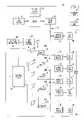
- FIG. 1is a block diagram of a memory device illustrating a voltage regulator servicing a number of output blocks
- FIG. 2is a circuit diagram of an output block of FIG. 1 ;
- FIG. 3is a circuit diagram illustrating one implementation of a voltage regulator constructed according to the teachings of the present invention.
- FIG. 4is a circuit diagram of control circuit used in conjunction with the voltage regulator of FIG. 3 ;
- FIG. 5is a circuit diagram of a circuit for controlling the decrease in bias voltage supplied to the differential amplifier of FIG. 3 ;
- FIG. 6illustrates an implementation for the output transistors of a data pre-river or the like.
- FIG. 7is a block diagram of a computer system in which the memory device of FIG. 1 may be used.
- FIG. 1illustrates a memory device 10 .
- the readerwill understand the description of the present invention in conjunction with the memory 10 of FIG. 1 is merely for purposes of providing one example of an application for the present invention. The present invention is not to be limited to the application shown in FIG. 1 .
- the memory device 10includes an array 12 of memory cells.
- the memory cells 12are arranged in rows and columns as is known in the art. Individual cells in the array 12 may be selected for a read or write operation by row decode circuitry 14 and column decode circuitry 16 which operates in response to command information on a command bus 18 and address information on an address bus 20 .
- Signals appearing on the command bus 18may include, but are not limited to, chip select, row address strobe, column address strobe, write enable and clock enable.
- Sense amps 22read information out of and write information into cells which have been selected by row decode circuitry 14 and column decode circuitry 16 in response to read and write commands, respectively.
- the sense amps 22form part of a data path shown generally by reference numeral 24 .
- the data path 24is the path along which data flows between a data bus 26 and the array 12 .
- the data pathbegins at data pads 28 and ends with sense amps 22 writing the data into the array 12 .
- the pathbegins with the sense amps reading the data from the array 12 and ends with the data being output on the data pads 28 .
- the data path 24is comprised of a number of circuits for buffering and amplifying the data which are not shown as they do not form a part of the present invention.
- a plurality of output blocks 30is arranged such that each output block 30 services one of the data pads 28 .
- An example of a typical output block 30is illustrated in FIG. 2 .
- the output block 30is comprised of a first plurality of enable transistors 31 , each connected in series with a drive transistor 32 .
- the transistors 31each receive the data signal q, while each of the drive transistors receives one of the Vgate enable signal EnVg ⁇ 0 >, EnVg ⁇ 1 > . . . EnVg ⁇ 6 >.
- the output blockis further comprised of a second plurality of enable transistors 33 , each connected in series with a drive transistor 32 .
- the first and second pluralities of enable transistors 31 , 33respectively, must be fully turned on by the signals q and q 1 for the drive transistors 32 to provide the proper pull-down load to the data pad 28 that it is servicing so that the voltage level necessary to represent the data being transferred is quickly reached.
- Each of the other output blocks 30may be identically constructed, and each receives the data signals q and q 1 and Vgate enable signals EnVg ⁇ 0 > through ⁇ 6 >.
- Each of the lines carrying the Vgate enable signals EnVg ⁇ 0 > through ⁇ 6 >is connected to a system voltage, V DD , through a p-channel transistor 34 .
- the gate of each of the transistors 34is connected to a control circuit 36 through an inverter 38 .
- the transistors 34thus provide a plurality of switches which, under the control of control circuit 36 , may momentarily connect the lines carrying the Vgate enable signals to the voltage source V DD .
- a voltage regulator 40provides the voltage for the Vgate enable signals through Vgate enable control 41 .
- Vgate enable control 41provides the Vgate enable signals to the output blocks 30 through a bus 42 .
- the bus 42is comprised of a plurality of lines each carrying one of the Vgate enable signals EnVg ⁇ 0 > through ⁇ 6 >.
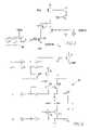
- FIG. 3a circuit diagram illustrating one implementation of the voltage regulator 40 constructed according to the present invention is illustrated.
- the voltage regulator 40has an output terminal 44 .
- a p-channel transistor 46is connected between a voltage source and the output terminal 44 and an n-channel transistor 48 is connected between the output terminal 44 and ground.
- a transistor 50receives at its gate terminal, through a pass gate 52 , the same signal (OUT 1 ) that the transistor 46 receives.
- the pass gate 52is operative in response to a boost signal produced by the control circuit 36 .
- the boost signalis also input to a gate terminal of a p-channel transistor 54 through an inverter 56 .
- the p-channel transistor 54is connected across a gate terminal of the p-channel transistor 50 and a voltage source.
- FIG. 4a circuit diagram of a control circuit 36 which may be used in conjunction with the voltage regulator of FIG. 3 is illustrated.
- a plurality of one-shot multivibrators 56is provided. Each of the one-shots is triggered if its corresponding Vgate enable signal is enabled through Vgate enable control 41 .
- An exemplary embodiment for one of the one-shots 56is illustrated at 56 ′.
- One-shot 56 ′receives a signal ⁇ 6 > indicative of the need to enable the Vgate enable signal EnVg ⁇ 6 >. When the signal ⁇ 6 > indicates the need to enable the signal EnVg ⁇ 6 >, and an enable signal V-GCC_EN is present, the one-shot 56 ′ produces an output pulse 58 .
- the output pulse 58is input to the transistor 34 through the inverter 38 shown in FIG. 1 to momentarily render the p-channel transistor 34 conductive. In that manner, the line carrying the signal EnVg ⁇ 6 > is momentarily connected to the voltage source V DD , with the time of connection being determined by the width of the pulse 58 .
- the other one-shots 56are similarly constructed and used to momentarily connect the other lines carrying the Vgate enable signals to the voltage source V DD .
- NOR gates 60 , 61 and 62are used to aggregate the pulses produced by the one-shots 56 .
- the outputs of the NOR gatesare input to a first logic gate 64 which is a NAND gate.
- the output of the NAND gate 64is connected to an input of a second gate which is a NOR gate 66 .
- the output of the NAND gate 64is also connected to a second input of the NOR gate 66 through a delay circuit 68 .
- the output of the delay circuit 68is connected to another input of the NOR gate 66 through a second delay circuit 70 .
- the boost signal described above in conjunction with FIG. 3is available at an output terminal of the NOR gate 66 . That signal may be delayed further by propagating it through a pair of inverters 71 and 72 .
- the operation of the circuitry described thus farwill now be explained.
- the Vgate level at output terminal 44 in FIG. 3may not recover sufficiently quickly.
- Two stepsare taken to boost the voltage.
- the first stepis to render the p-channel transistor 34 servicing the relevant line carrying the Vgate enable signal which has just been enabled momentarily conductive through use of the pulse 58 . That enables the individual line carrying the particular Vgate enable signal to be momentarily connected to the voltage source V DD .
- the plurality of transistors 34may be considered to be part of a booster circuit as their function is to momentarily boost the voltage available to the particular line carrying the Vgate enable signal which has just been enabled.
- the second step which is takenis described in conjunction with FIG. 3 .
- pass gate 52becomes conductive which renders transistor 50 conductive which gives the voltage regulator 40 much more pull-up capability.
- transistor 54is turned off.
- the voltage regulator 40has about a 20 millivolt higher Vgate regulation point. That helps Vgate hit its final value under heavy load conditions.
- the circuitry within the dotted box 74may also be considered to be part of a booster circuit comprised of a transistor 50 with the remaining components comprising a control circuit for controlling the conductivity of transistor 50 .
- booster circuit 75which is similar to the circuit 74 .
- the transistor 50becomes an n-channel transistor 50 ′.
- the control portion of the booster circuit 75is likewise changed as follows:
- the booster circuit comprised of the plurality of transistors 34is rendered operative so that one, some or all of the transistors 34 are rendered conductive to momentarily connect the line(s) carrying the Vgate enable signal(s) to a voltage source.
- the boost signalproduced under heavy load conditions, enables the output terminal 44 of the voltage regulator 40 to be sourced with additional current through booster circuit 74 in an unbalanced mode, or through booster circuits 74 and 75 in a balanced mode.
- the NAND gate 64produces a control pulse whenever it receives a low going pulse at one or more of its input terminals.
- the NAND gate 64will produce a control pulse whenever selected Vgate enable signals are initially enabled.
- the lowest three lines, lines 2 , 1 and 0can be optioned out by a switch 76 because the capacitance on those lines is so small that Vgate is not affected much when they turn on.
- the selection of other types of gates and other arrangements of gatescould cause the control pulse to be produced under different conditions.
- control pulse produced by the NAND gate 64is not of sufficient duration.
- the control pulseis input directly to the second gate 66 to cause the gate 66 to change states to a low state.
- the control pulseis also input to the gate 66 through the delay circuit 68 . In that manner, as the control pulse from gate 64 prepares to end, a delayed control pulse produced by delay circuit 68 becomes available at an input terminal of the gate 66 , thereby insuring that the output of the gate 66 does not change state.
- the delayed control pulse produced by the delay circuit 68is input to the second gate 66 through the delay circuit 70 such that when the delayed control pulse produced by the delay circuit 68 is preparing to end, the delayed control pulse produced by the delay circuit 70 is input to an input terminal of the gate 66 thereby insuring that the output of the gate 66 does not change when the delay pulse produced by the delay circuit 68 ends.
- a control pulse of extended durationcan be obtained at the output of the second gate 66 .
- Additional delay circuits 68 , 70can be added to increase the length of the control pulse of extended duration.
- the control pulse of extended durationis the boost signal which is input to the control portion of the booster circuit 74 .
- the delay circuits 68 and 70 together with the NOR gate 66may be viewed as a pulse extender.
- the pulse extender of the present inventionshould have outputs taken from enough points along the delay line to insure no glitch in the extended pulse.
- the voltage regulator 40may have a differential amplifier 78 which produces a first output signal, OUT 1 , for directly driving transistor 46 and a second output signal, OUT 2 , which indirectly drives transistor 48 .
- a bias voltageis supplied to the differential amplifier 78 through an n-channel transistor 82 .
- Transistor 82is responsive to a control signal VgRegBias.
- a transistor 84is connected in series with a transistor 85 , with the two transistors 84 and 85 connected in parallel with the transistor 82 .
- the boost signalmay be additionally used to control the transistor 84 . Because the boost signal is active low, an active high version is taken from the output of inverter 56 , such that when the boost signal is active, the transistor 84 is turned on.
- a one-shot 86is responsive to a signal VgNap which is responsible for putting the voltage regulator 40 into a nap or standby mode.
- the one-shot 86produces an output pulse which temporarily renders transistor 88 conductive.
- a transistor 90connected to operate as a diode, pulls the signal VgRegBias within a Vt of ground thereby causing it to decrease even more rapidly.
- the diode 90is no longer conductive as the transistor 88 is turned off. In that manner the reduction in bias voltage can be increased.
- a compensation resistor 92 and compensation capacitor 94which are a load across the transistor 46 , can keep the p-channel transistor 46 from reducing its drive sufficiently quickly.
- the pulse produced by the one-shot 86 of FIG. 5is used to pull a node 96 between the resistor 92 and capacitor 94 to a predefined voltage other than zero through a transistor 98 .
- the predefined voltageis V DD which allows transistor 46 to go to a low power mode very quickly. This actually shuts off the transistor 46 briefly, but because that shutoff occurs at the beginning of a nap or standby mode, the shutoff is a non-issue.
- the node 96could be pulled up to a large p-channel diode tied to V DD .
- the p-channel diodemust be sized such that it allows quick pullup while leaving transistor 46 on near steady state nap or standby conditions. That embodiment comes at a layout expense as the p-channel diode needs to be sufficiently large.
- the pre-driver circuit 100is constructed of a first data path 102 responsive to a data signal q and a second data path 104 responsive to a delayed version of the data signal q′ which is delayed by less than 180°.
- the first data path 102has two output transistor drive stages 106 and 108 while the second data path 104 similarly has two transistor output drive stages 110 and 112 .
- the transistors 106 and 110are enabled when a signal s 11 renders a transistor 114 conductive.
- the transistors 108 and 112are operative when a signal s 12 renders a transistor 116 conductive.
- three of the four two-bit codescan have different total amounts of p-channel drive enabled in the pre-driver 100 .
- more skewcan be eliminated from the subsequent output driver stages with the pre-driver 100 illustrated in FIG. 6 .
- FIG. 7illustrates a computer system 200 containing the memory of FIG. 1 .
- the computer system 200includes a processor 202 for performing various computing functions, such as executing specific software to perform specific calculations or tasks.
- the processor 202includes a processor bus 204 that normally includes an address bus, a control bus, and a data bus.
- the computer system 200includes one or more input devices 214 , such as a keyboard or a mouse, coupled to the processor 202 to allow an operator to interface with the computer system 200 .
- the computer system 200also includes one or more output devices 216 coupled to the processor 202 , such output devices typically being a printer or a video terminal.
- One or more data storage devices 218are also typically coupled to the processor 202 to allow the processor 202 to store data in or retrieve data from internal or external storage media (not shown). Examples of typical storage devices 218 include hard and floppy disks, tape cassettes, and compact disk read-only memories (CD-ROMs).
- the processor 202is also typically coupled to cache memory 226 , which is usually static random access memory (“SRAM”) and to an SDRAM 228 through a memory controller 230 .
- the memory controller 230normally includes a control bus 236 and an address bus 238 that may be coupled to the SDRAM 228 .
- a data bus 240may be coupled to the processor bus 204 either directly (as shown), through the memory controller 230 , or by some other means.
Landscapes
- Engineering & Computer Science (AREA)
- Power Engineering (AREA)
- Dram (AREA)
- Read Only Memory (AREA)
Abstract
Description
- the
transistor 54 becomes an n-channel transistor 54′. Thetransistors 50′ and54′ have their source and well connections to Vssand Vbb, respectively. The input to passgate 52′ is the same signal input to the gate oftransistor 48.Transistor 54′ receives the active low boost signal directly. The sizing of the various components comprising thebooster circuit 75 would be such that the offset would be nulled out.
- the
Claims (9)
Priority Applications (1)
| Application Number | Priority Date | Filing Date | Title |
|---|---|---|---|
| US10/678,595US7139203B2 (en) | 2000-08-31 | 2003-10-03 | Voltage regulator and data path for a memory device |
Applications Claiming Priority (3)
| Application Number | Priority Date | Filing Date | Title |
|---|---|---|---|
| US09/654,099US6545929B1 (en) | 2000-08-31 | 2000-08-31 | Voltage regulator and data path for a memory device |
| US09/792,554US20020064076A1 (en) | 2000-08-31 | 2001-02-23 | Voltage regulator and data path for a memory device |
| US10/678,595US7139203B2 (en) | 2000-08-31 | 2003-10-03 | Voltage regulator and data path for a memory device |
Related Parent Applications (1)
| Application Number | Title | Priority Date | Filing Date |
|---|---|---|---|
| US09/792,554ContinuationUS20020064076A1 (en) | 2000-08-31 | 2001-02-23 | Voltage regulator and data path for a memory device |
Publications (2)
| Publication Number | Publication Date |
|---|---|
| US20040156258A1 US20040156258A1 (en) | 2004-08-12 |
| US7139203B2true US7139203B2 (en) | 2006-11-21 |
Family
ID=24623424
Family Applications (9)
| Application Number | Title | Priority Date | Filing Date |
|---|---|---|---|
| US09/654,099Expired - LifetimeUS6545929B1 (en) | 2000-08-31 | 2000-08-31 | Voltage regulator and data path for a memory device |
| US09/792,553Expired - LifetimeUS6456556B1 (en) | 2000-08-31 | 2001-02-23 | Voltage regulator and data path for a memory device |
| US09/792,536Expired - LifetimeUS6466485B2 (en) | 2000-08-31 | 2001-02-23 | Voltage regulator and data path for a memory device |
| US09/792,554AbandonedUS20020064076A1 (en) | 2000-08-31 | 2001-02-23 | Voltage regulator and data path for a memory device |
| US09/792,537Expired - LifetimeUS6411562B1 (en) | 2000-08-31 | 2001-02-23 | Voltage regulator and data path for a memory device |
| US10/241,646AbandonedUS20030012056A1 (en) | 2000-08-31 | 2002-09-11 | Voltage regulator and data path for a memory device |
| US10/669,635Expired - LifetimeUS6885592B2 (en) | 2000-08-31 | 2003-09-24 | Voltage regulator and data path for a memory device |
| US10/678,595Expired - LifetimeUS7139203B2 (en) | 2000-08-31 | 2003-10-03 | Voltage regulator and data path for a memory device |
| US10/678,722Expired - LifetimeUS7016250B2 (en) | 2000-08-31 | 2003-10-03 | Voltage regulator and data path for a memory device |
Family Applications Before (7)
| Application Number | Title | Priority Date | Filing Date |
|---|---|---|---|
| US09/654,099Expired - LifetimeUS6545929B1 (en) | 2000-08-31 | 2000-08-31 | Voltage regulator and data path for a memory device |
| US09/792,553Expired - LifetimeUS6456556B1 (en) | 2000-08-31 | 2001-02-23 | Voltage regulator and data path for a memory device |
| US09/792,536Expired - LifetimeUS6466485B2 (en) | 2000-08-31 | 2001-02-23 | Voltage regulator and data path for a memory device |
| US09/792,554AbandonedUS20020064076A1 (en) | 2000-08-31 | 2001-02-23 | Voltage regulator and data path for a memory device |
| US09/792,537Expired - LifetimeUS6411562B1 (en) | 2000-08-31 | 2001-02-23 | Voltage regulator and data path for a memory device |
| US10/241,646AbandonedUS20030012056A1 (en) | 2000-08-31 | 2002-09-11 | Voltage regulator and data path for a memory device |
| US10/669,635Expired - LifetimeUS6885592B2 (en) | 2000-08-31 | 2003-09-24 | Voltage regulator and data path for a memory device |
Family Applications After (1)
| Application Number | Title | Priority Date | Filing Date |
|---|---|---|---|
| US10/678,722Expired - LifetimeUS7016250B2 (en) | 2000-08-31 | 2003-10-03 | Voltage regulator and data path for a memory device |
Country Status (1)
| Country | Link |
|---|---|
| US (9) | US6545929B1 (en) |
Cited By (1)
| Publication number | Priority date | Publication date | Assignee | Title |
|---|---|---|---|---|
| US20100128551A1 (en)* | 2008-11-26 | 2010-05-27 | Micron Technology, Inc. | Adjustable voltage regulator for providing a regulated output voltage |
Families Citing this family (14)
| Publication number | Priority date | Publication date | Assignee | Title |
|---|---|---|---|---|
| JP4974202B2 (en)* | 2001-09-19 | 2012-07-11 | ルネサスエレクトロニクス株式会社 | Semiconductor integrated circuit |
| US6717927B2 (en)* | 2002-04-05 | 2004-04-06 | Interdigital Technology Corporation | System for efficient recovery of node B buffered data following serving high speed downlink shared channel cell change |
| GB0212041D0 (en)* | 2002-05-24 | 2002-07-03 | Sendo Int Ltd | USB circuit arrangement |
| US20050088222A1 (en)* | 2003-10-27 | 2005-04-28 | Stmicroelectronics, Inc. | Chip enabled voltage regulator |
| US7086139B2 (en)* | 2004-04-30 | 2006-08-08 | Hitachi Global Storage Technologies Netherlands B.V. | Methods of making magnetic write heads using electron beam lithography |
| US7206234B2 (en)* | 2005-06-21 | 2007-04-17 | Micron Technology, Inc. | Input buffer for low voltage operation |
| KR100818703B1 (en)* | 2005-06-29 | 2008-04-01 | 주식회사 하이닉스반도체 | Voltage pumping device |
| US7565457B2 (en)* | 2006-06-30 | 2009-07-21 | Intel Corporation | Serial advanced technology attachment device presence detection and hot-plug in low power mode |
| JP5253901B2 (en) | 2008-06-20 | 2013-07-31 | 株式会社東芝 | Memory system |
| KR20100104182A (en)* | 2009-03-17 | 2010-09-29 | 주식회사 하이닉스반도체 | Semiconductor apparatus and data output method of the same |
| US8125211B2 (en) | 2009-06-09 | 2012-02-28 | Apple Inc. | Apparatus and method for testing driver writeability strength on an integrated circuit |
| US8248880B2 (en)* | 2010-03-29 | 2012-08-21 | Micron Technology, Inc. | Voltage regulators, amplifiers, memory devices and methods |
| KR20120098303A (en)* | 2011-02-28 | 2012-09-05 | 에스케이하이닉스 주식회사 | Data transmission circuit |
| CN103905028B (en)* | 2012-12-25 | 2018-05-25 | 中芯国际集成电路制造(上海)有限公司 | Signal receiver and signal transmission apparatus |
Citations (16)
| Publication number | Priority date | Publication date | Assignee | Title |
|---|---|---|---|---|
| US5010256A (en)* | 1989-02-21 | 1991-04-23 | United Technologies Corporation | Gate output driver using slew-rate control |
| US5285116A (en)* | 1990-08-28 | 1994-02-08 | Mips Computer Systems, Inc. | Low-noise high-speed output buffer and method for controlling same |
| US5420467A (en) | 1992-01-31 | 1995-05-30 | International Business Machines Corporation | Programmable delay clock chopper/stretcher with fast recovery |
| US5576656A (en) | 1994-12-20 | 1996-11-19 | Sgs-Thomson Microelectronics, Inc. | Voltage regulator for an output driver with reduced output impedance |
| US5596297A (en) | 1994-12-20 | 1997-01-21 | Sgs-Thomson Microelectronics, Inc. | Output driver circuitry with limited output high voltage |
| US5619456A (en)* | 1996-01-19 | 1997-04-08 | Sgs-Thomson Microelectronics, Inc. | Synchronous output circuit |
| US5666078A (en)* | 1996-02-07 | 1997-09-09 | International Business Machines Corporation | Programmable impedance output driver |
| US5706240A (en) | 1992-06-30 | 1998-01-06 | Sgs-Thomson Microelectronics S.R.L. | Voltage regulator for memory device |
| US5798970A (en)* | 1996-02-01 | 1998-08-25 | Micron Technology, Inc. | Memory device output buffer |
| US5850139A (en) | 1997-02-28 | 1998-12-15 | Stmicroelectronics, Inc. | Load pole stabilized voltage regulator circuit |
| US5909150A (en) | 1997-10-23 | 1999-06-01 | Cirrus Logic, Inc. | System and method for improving the regulation of a supply voltage for a controllable oscillator using feed forward control techniques |
| US5955915A (en) | 1995-03-28 | 1999-09-21 | Stmicroelectronics, Inc. | Circuit for limiting the current in a power transistor |
| US5998981A (en) | 1997-06-03 | 1999-12-07 | International Business Machines Corporation | Weak inversion NMOS regulator with boosted gate |
| US6060907A (en)* | 1997-06-25 | 2000-05-09 | Sun Microsystems, Inc. | Impedance control circuit |
| US6100744A (en) | 1997-09-04 | 2000-08-08 | Samsung Electronics Co., Ltd. | Integrated circuit devices having improved internal voltage generators which reduce timing skew in buffer circuits therein |
| US6114885A (en)* | 1997-08-22 | 2000-09-05 | Samsung Electronics Co., Ltd. | Integrated driver circuits having independently programmable pull-up and pull-down circuits therein which match load impedance |
Family Cites Families (1)
| Publication number | Priority date | Publication date | Assignee | Title |
|---|---|---|---|---|
| US4975598A (en)* | 1988-12-21 | 1990-12-04 | Intel Corporation | Temperature, voltage, and process compensated output driver |
- 2000
- 2000-08-31USUS09/654,099patent/US6545929B1/ennot_activeExpired - Lifetime
- 2001
- 2001-02-23USUS09/792,553patent/US6456556B1/ennot_activeExpired - Lifetime
- 2001-02-23USUS09/792,536patent/US6466485B2/ennot_activeExpired - Lifetime
- 2001-02-23USUS09/792,554patent/US20020064076A1/ennot_activeAbandoned
- 2001-02-23USUS09/792,537patent/US6411562B1/ennot_activeExpired - Lifetime
- 2002
- 2002-09-11USUS10/241,646patent/US20030012056A1/ennot_activeAbandoned
- 2003
- 2003-09-24USUS10/669,635patent/US6885592B2/ennot_activeExpired - Lifetime
- 2003-10-03USUS10/678,595patent/US7139203B2/ennot_activeExpired - Lifetime
- 2003-10-03USUS10/678,722patent/US7016250B2/ennot_activeExpired - Lifetime
Patent Citations (16)
| Publication number | Priority date | Publication date | Assignee | Title |
|---|---|---|---|---|
| US5010256A (en)* | 1989-02-21 | 1991-04-23 | United Technologies Corporation | Gate output driver using slew-rate control |
| US5285116A (en)* | 1990-08-28 | 1994-02-08 | Mips Computer Systems, Inc. | Low-noise high-speed output buffer and method for controlling same |
| US5420467A (en) | 1992-01-31 | 1995-05-30 | International Business Machines Corporation | Programmable delay clock chopper/stretcher with fast recovery |
| US5706240A (en) | 1992-06-30 | 1998-01-06 | Sgs-Thomson Microelectronics S.R.L. | Voltage regulator for memory device |
| US5576656A (en) | 1994-12-20 | 1996-11-19 | Sgs-Thomson Microelectronics, Inc. | Voltage regulator for an output driver with reduced output impedance |
| US5596297A (en) | 1994-12-20 | 1997-01-21 | Sgs-Thomson Microelectronics, Inc. | Output driver circuitry with limited output high voltage |
| US5955915A (en) | 1995-03-28 | 1999-09-21 | Stmicroelectronics, Inc. | Circuit for limiting the current in a power transistor |
| US5619456A (en)* | 1996-01-19 | 1997-04-08 | Sgs-Thomson Microelectronics, Inc. | Synchronous output circuit |
| US5798970A (en)* | 1996-02-01 | 1998-08-25 | Micron Technology, Inc. | Memory device output buffer |
| US5666078A (en)* | 1996-02-07 | 1997-09-09 | International Business Machines Corporation | Programmable impedance output driver |
| US5850139A (en) | 1997-02-28 | 1998-12-15 | Stmicroelectronics, Inc. | Load pole stabilized voltage regulator circuit |
| US5998981A (en) | 1997-06-03 | 1999-12-07 | International Business Machines Corporation | Weak inversion NMOS regulator with boosted gate |
| US6060907A (en)* | 1997-06-25 | 2000-05-09 | Sun Microsystems, Inc. | Impedance control circuit |
| US6114885A (en)* | 1997-08-22 | 2000-09-05 | Samsung Electronics Co., Ltd. | Integrated driver circuits having independently programmable pull-up and pull-down circuits therein which match load impedance |
| US6100744A (en) | 1997-09-04 | 2000-08-08 | Samsung Electronics Co., Ltd. | Integrated circuit devices having improved internal voltage generators which reduce timing skew in buffer circuits therein |
| US5909150A (en) | 1997-10-23 | 1999-06-01 | Cirrus Logic, Inc. | System and method for improving the regulation of a supply voltage for a controllable oscillator using feed forward control techniques |
Cited By (4)
| Publication number | Priority date | Publication date | Assignee | Title |
|---|---|---|---|---|
| US20100128551A1 (en)* | 2008-11-26 | 2010-05-27 | Micron Technology, Inc. | Adjustable voltage regulator for providing a regulated output voltage |
| US7764563B2 (en)* | 2008-11-26 | 2010-07-27 | Micron Technology, Inc. | Adjustable voltage regulator for providing a regulated output voltage |
| US20100270994A1 (en)* | 2008-11-26 | 2010-10-28 | Micron Technology, Inc. | Adjustable voltage regulator for providing a regulated output voltage |
| US7957214B2 (en) | 2008-11-26 | 2011-06-07 | Micron Technology, Inc. | Adjustable voltage regulator for providing a regulated output voltage |
Also Published As
| Publication number | Publication date |
|---|---|
| US6411562B1 (en) | 2002-06-25 |
| US6466485B2 (en) | 2002-10-15 |
| US20020064076A1 (en) | 2002-05-30 |
| US6885592B2 (en) | 2005-04-26 |
| US7016250B2 (en) | 2006-03-21 |
| US20040160840A1 (en) | 2004-08-19 |
| US20040170080A1 (en) | 2004-09-02 |
| US20030012056A1 (en) | 2003-01-16 |
| US20040156258A1 (en) | 2004-08-12 |
| US6456556B1 (en) | 2002-09-24 |
| US20020048188A1 (en) | 2002-04-25 |
| US20020024867A1 (en) | 2002-02-28 |
| US20020024866A1 (en) | 2002-02-28 |
| US6545929B1 (en) | 2003-04-08 |
Similar Documents
| Publication | Publication Date | Title |
|---|---|---|
| US7139203B2 (en) | Voltage regulator and data path for a memory device | |
| KR100567916B1 (en) | Power supply device and method for semiconductor memory devices | |
| US6771550B2 (en) | Semiconductor memory device with stable precharge voltage level of data lines | |
| US9350351B2 (en) | Signal driver circuit having adjustable output voltage for a high logic level output signal | |
| US7511534B1 (en) | Circuits, devices, systems, and methods of operation for a linear output driver | |
| US20130258789A1 (en) | Semiconductor memory and method of operating semiconductor memory | |
| US6762968B2 (en) | Semiconductor memory device having a small-sized memory chip and a decreased power-supply noise | |
| US8750014B2 (en) | Tri-state driver circuits having automatic high-impedance enabling | |
| JP2845212B2 (en) | Semiconductor storage device | |
| KR20010025982A (en) | Sense amplifier of semiconductor memory device | |
| US6421297B1 (en) | Data-pattern-dependent compensation technique to maintain drive strength of an output driver | |
| US6928006B2 (en) | Semiconductor memory device capable of reducing noise during operation thereof | |
| US10373655B2 (en) | Apparatuses and methods for providing bias signals according to operation modes as supply voltages vary in a semiconductor device | |
| US5353249A (en) | Non-volatile semiconductor memory device | |
| KR100483026B1 (en) | Semiconductor memory device | |
| US5896320A (en) | Semiconductor memory device | |
| US6917550B2 (en) | Semiconductor memory device | |
| KR100406542B1 (en) | Sense amplifier controller and method thereof in semiconductor memory device | |
| KR100842899B1 (en) | Current sense amplifier circuit | |
| KR960006384B1 (en) | Pull-down circuit for wide voltage operation | |
| CN113948127A (en) | Apparatus having a driving circuit for overwriting data latched in a sense amplifier | |
| KR20030023339A (en) | Semiconductor memory device | |
| JP2000003592A (en) | Semiconductor storage device |
Legal Events
| Date | Code | Title | Description |
|---|---|---|---|
| FEPP | Fee payment procedure | Free format text:PAYOR NUMBER ASSIGNED (ORIGINAL EVENT CODE: ASPN); ENTITY STATUS OF PATENT OWNER: LARGE ENTITY | |
| STCF | Information on status: patent grant | Free format text:PATENTED CASE | |
| CC | Certificate of correction | ||
| FPAY | Fee payment | Year of fee payment:4 | |
| FPAY | Fee payment | Year of fee payment:8 | |
| AS | Assignment | Owner name:U.S. BANK NATIONAL ASSOCIATION, AS COLLATERAL AGENT, CALIFORNIA Free format text:SECURITY INTEREST;ASSIGNOR:MICRON TECHNOLOGY, INC.;REEL/FRAME:038669/0001 Effective date:20160426 Owner name:U.S. BANK NATIONAL ASSOCIATION, AS COLLATERAL AGEN Free format text:SECURITY INTEREST;ASSIGNOR:MICRON TECHNOLOGY, INC.;REEL/FRAME:038669/0001 Effective date:20160426 | |
| AS | Assignment | Owner name:MORGAN STANLEY SENIOR FUNDING, INC., AS COLLATERAL AGENT, MARYLAND Free format text:PATENT SECURITY AGREEMENT;ASSIGNOR:MICRON TECHNOLOGY, INC.;REEL/FRAME:038954/0001 Effective date:20160426 Owner name:MORGAN STANLEY SENIOR FUNDING, INC., AS COLLATERAL Free format text:PATENT SECURITY AGREEMENT;ASSIGNOR:MICRON TECHNOLOGY, INC.;REEL/FRAME:038954/0001 Effective date:20160426 | |
| AS | Assignment | Owner name:U.S. BANK NATIONAL ASSOCIATION, AS COLLATERAL AGENT, CALIFORNIA Free format text:CORRECTIVE ASSIGNMENT TO CORRECT THE REPLACE ERRONEOUSLY FILED PATENT #7358718 WITH THE CORRECT PATENT #7358178 PREVIOUSLY RECORDED ON REEL 038669 FRAME 0001. ASSIGNOR(S) HEREBY CONFIRMS THE SECURITY INTEREST;ASSIGNOR:MICRON TECHNOLOGY, INC.;REEL/FRAME:043079/0001 Effective date:20160426 Owner name:U.S. BANK NATIONAL ASSOCIATION, AS COLLATERAL AGEN Free format text:CORRECTIVE ASSIGNMENT TO CORRECT THE REPLACE ERRONEOUSLY FILED PATENT #7358718 WITH THE CORRECT PATENT #7358178 PREVIOUSLY RECORDED ON REEL 038669 FRAME 0001. ASSIGNOR(S) HEREBY CONFIRMS THE SECURITY INTEREST;ASSIGNOR:MICRON TECHNOLOGY, INC.;REEL/FRAME:043079/0001 Effective date:20160426 | |
| MAFP | Maintenance fee payment | Free format text:PAYMENT OF MAINTENANCE FEE, 12TH YEAR, LARGE ENTITY (ORIGINAL EVENT CODE: M1553) Year of fee payment:12 | |
| AS | Assignment | Owner name:JPMORGAN CHASE BANK, N.A., AS COLLATERAL AGENT, ILLINOIS Free format text:SECURITY INTEREST;ASSIGNORS:MICRON TECHNOLOGY, INC.;MICRON SEMICONDUCTOR PRODUCTS, INC.;REEL/FRAME:047540/0001 Effective date:20180703 Owner name:JPMORGAN CHASE BANK, N.A., AS COLLATERAL AGENT, IL Free format text:SECURITY INTEREST;ASSIGNORS:MICRON TECHNOLOGY, INC.;MICRON SEMICONDUCTOR PRODUCTS, INC.;REEL/FRAME:047540/0001 Effective date:20180703 | |
| AS | Assignment | Owner name:MICRON TECHNOLOGY, INC., IDAHO Free format text:RELEASE BY SECURED PARTY;ASSIGNOR:U.S. BANK NATIONAL ASSOCIATION, AS COLLATERAL AGENT;REEL/FRAME:047243/0001 Effective date:20180629 | |
| AS | Assignment | Owner name:MICRON TECHNOLOGY, INC., IDAHO Free format text:RELEASE BY SECURED PARTY;ASSIGNOR:MORGAN STANLEY SENIOR FUNDING, INC., AS COLLATERAL AGENT;REEL/FRAME:050937/0001 Effective date:20190731 | |
| AS | Assignment | Owner name:MICRON SEMICONDUCTOR PRODUCTS, INC., IDAHO Free format text:RELEASE BY SECURED PARTY;ASSIGNOR:JPMORGAN CHASE BANK, N.A., AS COLLATERAL AGENT;REEL/FRAME:051028/0001 Effective date:20190731 Owner name:MICRON TECHNOLOGY, INC., IDAHO Free format text:RELEASE BY SECURED PARTY;ASSIGNOR:JPMORGAN CHASE BANK, N.A., AS COLLATERAL AGENT;REEL/FRAME:051028/0001 Effective date:20190731 |