US7138681B2 - High density stepped, non-planar nitride read only memory - Google Patents
High density stepped, non-planar nitride read only memoryDownload PDFInfo
- Publication number
- US7138681B2 US7138681B2US10/899,906US89990604AUS7138681B2US 7138681 B2US7138681 B2US 7138681B2US 89990604 AUS89990604 AUS 89990604AUS 7138681 B2US7138681 B2US 7138681B2
- Authority
- US
- United States
- Prior art keywords
- array
- memory
- oxide
- memory cells
- substrate
- Prior art date
- Legal status (The legal status is an assumption and is not a legal conclusion. Google has not performed a legal analysis and makes no representation as to the accuracy of the status listed.)
- Expired - Lifetime, expires
Links
- 150000004767nitridesChemical class0.000titleclaimsabstractdescription19
- 230000015654memoryEffects0.000titleclaimsdescription70
- 239000000758substrateSubstances0.000claimsabstractdescription54
- 238000003860storageMethods0.000claimsabstractdescription14
- VYPSYNLAJGMNEJ-UHFFFAOYSA-NSilicium dioxideChemical compoundO=[Si]=OVYPSYNLAJGMNEJ-UHFFFAOYSA-N0.000claimsdescription24
- 239000012212insulatorSubstances0.000claimsdescription24
- 229910052710siliconInorganic materials0.000claimsdescription22
- 239000010703siliconSubstances0.000claimsdescription22
- XUIMIQQOPSSXEZ-UHFFFAOYSA-NSiliconChemical compound[Si]XUIMIQQOPSSXEZ-UHFFFAOYSA-N0.000claimsdescription20
- 239000000377silicon dioxideSubstances0.000claimsdescription11
- TWNQGVIAIRXVLR-UHFFFAOYSA-Noxo(oxoalumanyloxy)alumaneChemical compoundO=[Al]O[Al]=OTWNQGVIAIRXVLR-UHFFFAOYSA-N0.000claimsdescription10
- 239000002131composite materialSubstances0.000claimsdescription9
- 239000003989dielectric materialSubstances0.000claimsdescription6
- 235000012239silicon dioxideNutrition0.000claimsdescription4
- 238000009279wet oxidation reactionMethods0.000claimsdescription2
- 230000008878couplingEffects0.000claims1
- 238000010168coupling processMethods0.000claims1
- 238000005859coupling reactionMethods0.000claims1
- 239000010410layerSubstances0.000description41
- 239000010408filmSubstances0.000description19
- 238000000034methodMethods0.000description19
- GWEVSGVZZGPLCZ-UHFFFAOYSA-NTitan oxideChemical compoundO=[Ti]=OGWEVSGVZZGPLCZ-UHFFFAOYSA-N0.000description10
- 238000001704evaporationMethods0.000description10
- 230000008020evaporationEffects0.000description9
- MCMNRKCIXSYSNV-UHFFFAOYSA-NZirconium dioxideChemical compoundO=[Zr]=OMCMNRKCIXSYSNV-UHFFFAOYSA-N0.000description8
- 238000000151depositionMethods0.000description8
- 238000000231atomic layer depositionMethods0.000description7
- 230000008021depositionEffects0.000description7
- 238000010849ion bombardmentMethods0.000description7
- 238000004519manufacturing processMethods0.000description7
- 229910052751metalInorganic materials0.000description7
- 239000002184metalSubstances0.000description7
- 230000003647oxidationEffects0.000description6
- 238000007254oxidation reactionMethods0.000description6
- 239000002243precursorSubstances0.000description6
- 239000004065semiconductorSubstances0.000description6
- 239000002800charge carrierSubstances0.000description5
- 238000005516engineering processMethods0.000description5
- 238000002347injectionMethods0.000description5
- 239000007924injectionSubstances0.000description5
- 239000001301oxygenSubstances0.000description5
- 229910052760oxygenInorganic materials0.000description5
- 238000002207thermal evaporationMethods0.000description5
- 229910052727yttriumInorganic materials0.000description5
- 229910052688GadoliniumInorganic materials0.000description4
- QVGXLLKOCUKJST-UHFFFAOYSA-Natomic oxygenChemical compound[O]QVGXLLKOCUKJST-UHFFFAOYSA-N0.000description4
- 238000005566electron beam evaporationMethods0.000description4
- 238000007667floatingMethods0.000description4
- CJNBYAVZURUTKZ-UHFFFAOYSA-Nhafnium(IV) oxideInorganic materialsO=[Hf]=OCJNBYAVZURUTKZ-UHFFFAOYSA-N0.000description4
- 239000002784hot electronSubstances0.000description4
- 229910021420polycrystalline siliconInorganic materials0.000description4
- 229920005591polysiliconPolymers0.000description4
- 239000010409thin filmSubstances0.000description4
- -1CrTiO3Inorganic materials0.000description3
- 229910002244LaAlO3Inorganic materials0.000description3
- 229910018557Si OInorganic materials0.000description3
- 238000006243chemical reactionMethods0.000description3
- CMIHHWBVHJVIGI-UHFFFAOYSA-Ngadolinium(III) oxideInorganic materials[O-2].[O-2].[O-2].[Gd+3].[Gd+3]CMIHHWBVHJVIGI-UHFFFAOYSA-N0.000description3
- 239000000463materialSubstances0.000description3
- 239000011159matrix materialSubstances0.000description3
- LIVNPJMFVYWSIS-UHFFFAOYSA-Nsilicon monoxideInorganic materials[Si-]#[O+]LIVNPJMFVYWSIS-UHFFFAOYSA-N0.000description3
- 238000004544sputter depositionMethods0.000description3
- 230000005641tunnelingEffects0.000description3
- RUDFQVOCFDJEEF-UHFFFAOYSA-Nyttrium(III) oxideInorganic materials[O-2].[O-2].[O-2].[Y+3].[Y+3]RUDFQVOCFDJEEF-UHFFFAOYSA-N0.000description3
- XKRFYHLGVUSROY-UHFFFAOYSA-NArgonChemical compound[Ar]XKRFYHLGVUSROY-UHFFFAOYSA-N0.000description2
- MHAJPDPJQMAIIY-UHFFFAOYSA-NHydrogen peroxideChemical compoundOOMHAJPDPJQMAIIY-UHFFFAOYSA-N0.000description2
- GQPLMRYTRLFLPF-UHFFFAOYSA-NNitrous OxideChemical compound[O-][N+]#NGQPLMRYTRLFLPF-UHFFFAOYSA-N0.000description2
- CBENFWSGALASAD-UHFFFAOYSA-NOzoneChemical compound[O-][O+]=OCBENFWSGALASAD-UHFFFAOYSA-N0.000description2
- 229910052581Si3N4Inorganic materials0.000description2
- 230000006978adaptationEffects0.000description2
- 230000003247decreasing effectEffects0.000description2
- 238000010586diagramMethods0.000description2
- 230000000694effectsEffects0.000description2
- 150000002500ionsChemical class0.000description2
- MRELNEQAGSRDBK-UHFFFAOYSA-Nlanthanum oxideInorganic materials[O-2].[O-2].[O-2].[La+3].[La+3]MRELNEQAGSRDBK-UHFFFAOYSA-N0.000description2
- 238000001465metallisationMethods0.000description2
- 239000000203mixtureSubstances0.000description2
- 239000002105nanoparticleSubstances0.000description2
- KTUFCUMIWABKDW-UHFFFAOYSA-Noxo(oxolanthaniooxy)lanthanumChemical compoundO=[La]O[La]=OKTUFCUMIWABKDW-UHFFFAOYSA-N0.000description2
- 239000008188pelletSubstances0.000description2
- HQVNEWCFYHHQES-UHFFFAOYSA-Nsilicon nitrideChemical compoundN12[Si]34N5[Si]62N3[Si]51N64HQVNEWCFYHHQES-UHFFFAOYSA-N0.000description2
- 229910052814silicon oxideInorganic materials0.000description2
- 239000002356single layerSubstances0.000description2
- 239000010936titaniumSubstances0.000description2
- 229910017107AlOxInorganic materials0.000description1
- 206010021143HypoxiaDiseases0.000description1
- 229910003074TiCl4Inorganic materials0.000description1
- 229910003087TiOxInorganic materials0.000description1
- RTAQQCXQSZGOHL-UHFFFAOYSA-NTitaniumChemical compound[Ti]RTAQQCXQSZGOHL-UHFFFAOYSA-N0.000description1
- 229910003077Ti−OInorganic materials0.000description1
- 229910006252ZrONInorganic materials0.000description1
- 229910003134ZrOxInorganic materials0.000description1
- 150000001298alcoholsChemical class0.000description1
- 229910045601alloyInorganic materials0.000description1
- 239000000956alloySubstances0.000description1
- 229910052786argonInorganic materials0.000description1
- 230000015572biosynthetic processEffects0.000description1
- 239000006227byproductSubstances0.000description1
- 239000000969carrierSubstances0.000description1
- 230000001413cellular effectEffects0.000description1
- 238000010549co-EvaporationMethods0.000description1
- 238000004891communicationMethods0.000description1
- 238000011109contaminationMethods0.000description1
- 238000007796conventional methodMethods0.000description1
- 239000013078crystalSubstances0.000description1
- 230000005684electric fieldEffects0.000description1
- 238000010894electron beam technologyMethods0.000description1
- 238000000313electron-beam-induced depositionMethods0.000description1
- 238000011066ex-situ storageMethods0.000description1
- 230000005284excitationEffects0.000description1
- 230000002349favourable effectEffects0.000description1
- 230000006870functionEffects0.000description1
- 239000007789gasSubstances0.000description1
- 238000010438heat treatmentMethods0.000description1
- 239000011261inert gasSubstances0.000description1
- 238000010884ion-beam techniqueMethods0.000description1
- 229910052743kryptonInorganic materials0.000description1
- DNNSSWSSYDEUBZ-UHFFFAOYSA-Nkrypton atomChemical compound[Kr]DNNSSWSSYDEUBZ-UHFFFAOYSA-N0.000description1
- 229910052746lanthanumInorganic materials0.000description1
- 150000002739metalsChemical class0.000description1
- 239000001272nitrous oxideSubstances0.000description1
- 238000010926purgeMethods0.000description1
- 238000000746purificationMethods0.000description1
- 238000004151rapid thermal annealingMethods0.000description1
- 229910052594sapphireInorganic materials0.000description1
- 239000010980sapphireSubstances0.000description1
- 238000000926separation methodMethods0.000description1
- HBMJWWWQQXIZIP-UHFFFAOYSA-Nsilicon carbideChemical compound[Si+]#[C-]HBMJWWWQQXIZIP-UHFFFAOYSA-N0.000description1
- 229910010271silicon carbideInorganic materials0.000description1
- 238000005549size reductionMethods0.000description1
- 239000007858starting materialSubstances0.000description1
- 230000001360synchronised effectEffects0.000description1
- 229910052715tantalumInorganic materials0.000description1
- GUVRBAGPIYLISA-UHFFFAOYSA-Ntantalum atomChemical compound[Ta]GUVRBAGPIYLISA-UHFFFAOYSA-N0.000description1
- HLLICFJUWSZHRJ-UHFFFAOYSA-NtioxidazoleChemical compoundCCCOC1=CC=C2N=C(NC(=O)OC)SC2=C1HLLICFJUWSZHRJ-UHFFFAOYSA-N0.000description1
- 229910052719titaniumInorganic materials0.000description1
- XJDNKRIXUMDJCW-UHFFFAOYSA-Jtitanium tetrachlorideChemical compoundCl[Ti](Cl)(Cl)ClXJDNKRIXUMDJCW-UHFFFAOYSA-J0.000description1
- 238000009827uniform distributionMethods0.000description1
- XLYOFNOQVPJJNP-UHFFFAOYSA-NwaterSubstancesOXLYOFNOQVPJJNP-UHFFFAOYSA-N0.000description1
- VWQVUPCCIRVNHF-UHFFFAOYSA-Nyttrium atomChemical compound[Y]VWQVUPCCIRVNHF-UHFFFAOYSA-N0.000description1
Images


Classifications
- G—PHYSICS
- G11—INFORMATION STORAGE
- G11C—STATIC STORES
- G11C16/00—Erasable programmable read-only memories
- G11C16/02—Erasable programmable read-only memories electrically programmable
- G11C16/04—Erasable programmable read-only memories electrically programmable using variable threshold transistors, e.g. FAMOS
- G11C16/0466—Erasable programmable read-only memories electrically programmable using variable threshold transistors, e.g. FAMOS comprising cells with charge storage in an insulating layer, e.g. metal-nitride-oxide-silicon [MNOS], silicon-oxide-nitride-oxide-silicon [SONOS]
- G11C16/0475—Erasable programmable read-only memories electrically programmable using variable threshold transistors, e.g. FAMOS comprising cells with charge storage in an insulating layer, e.g. metal-nitride-oxide-silicon [MNOS], silicon-oxide-nitride-oxide-silicon [SONOS] comprising two or more independent storage sites which store independent data
- H—ELECTRICITY
- H10—SEMICONDUCTOR DEVICES; ELECTRIC SOLID-STATE DEVICES NOT OTHERWISE PROVIDED FOR
- H10B—ELECTRONIC MEMORY DEVICES
- H10B43/00—EEPROM devices comprising charge-trapping gate insulators
- H10B43/30—EEPROM devices comprising charge-trapping gate insulators characterised by the memory core region
- H—ELECTRICITY
- H10—SEMICONDUCTOR DEVICES; ELECTRIC SOLID-STATE DEVICES NOT OTHERWISE PROVIDED FOR
- H10B—ELECTRONIC MEMORY DEVICES
- H10B69/00—Erasable-and-programmable ROM [EPROM] devices not provided for in groups H10B41/00 - H10B63/00, e.g. ultraviolet erasable-and-programmable ROM [UVEPROM] devices
Definitions
- the present inventionrelates generally to memory devices and in particular the present invention relates to an NROM device architecture.
- RAMrandom-access memory
- ROMread only memory
- DRAMdynamic random access memory
- SDRAMsynchronous dynamic random access memory
- flash memoryflash memory
- Flash memory deviceshave developed into a popular source of non-volatile memory for a wide range of electronic applications. Flash memory devices typically use a one-transistor memory cell that allows for high memory densities, high reliability, and low power consumption. Common uses for flash memory include personal computers, personal digital assistants (PDAs), digital cameras, and cellular telephones. Program code and system data such as a basic input/output system (BIOS) are typically stored in flash memory devices for use in personal computer systems.
- BIOSbasic input/output system
- FIG. 1shows a cross-section of a typical prior art NROM array.
- the arrayis comprised of a silicon substrate 100 with a gate oxide layer 101 formed over the substrate 100 .
- a silicon nitride layer 102is formed over the gate oxide 101 .
- Each transistor 140 – 142is comprised of two charge storage regions 110 and 111 in the nitride layer 102 .
- An intergate insulator 107is formed over the nitride layer 102 prior to forming the control gate/wordline 120 – 122 of each transistor 140 – 142 over the intergate insulator 107 and substantially between the source/drain regions 130 – 133 .
- the minimum feature size of the transistors 140 – 142 of FIG. 1is described by F.
- the densityis therefore one bit for each 4F 2 units surface area. This is typically described as a density of 4F 2 /bit.
- the computer componentsshould also go through a corresponding size reduction and performance increase.
- the transistorscan be reduced in size. This has the effect of increased speed and memory density with decreased power requirements.
- flash memory cell technologieshave some scaling limitations due to the high voltage requirements for program and erase operations.
- MOSFETsare scaled to deep sub-micron dimensions, it becomes more difficult to maintain an acceptable aspect ratio.
- the gate oxide thicknessscaled to less than 10 nm as the channel length becomes sub-micron but the depletion region width and junction depth must be scaled to smaller dimensions.
- the present inventionencompasses a stepped, non-planar NROM array.
- the arrayis comprised of a trenched substrate with steps between adjacent transistors along a column of series connected transistors. Adjacent column transistors, fabricated on both the pillars and in the first set of trenches, are coupled through source/drain regions that are shared.
- Each of the NROM cellshas a nitride layer with a plurality of charge storage regions.
- the columnsare separated from adjacent columns by another set of trenches that are substantially perpendicular to the first set of trenches.
- Each row of the arrayis coupled by a wordline that runs substantially parallel to the first set of trenches and couples the transistors in that row. Adjacent rows of the array are on different planes.
- FIG. 1shows a cross-sectional view of a typical prior art planar NAND NROM array.
- FIG. 2shows a cross-sectional view of one embodiment of a non-planar, stepped NROM array of the present invention.
- FIG. 3shows a cross-sectional view of fabrication steps for one embodiment of the present invention in accordance with the array of FIG. 2 .
- FIG. 4shows a cross-sectional view of additional steps for one embodiment of the fabrication method of the present invention in accordance with the array of FIG. 2 .
- FIG. 5shows a cross-sectional view of additional steps for one embodiment of the fabrication method of the present invention in accordance with the array of FIG. 2 .
- FIG. 6shows a three dimensional, cross-sectional view of one embodiment of the array of FIG. 2 .
- FIG. 7shows a block diagram of an electronic system that incorporates the non-planar, stepped NROM array of the present invention.
- SOSsilicon-on-sapphire
- SOIsilicon-on-insulator
- TFTthin film transistor
- doped and undoped semiconductorsepitaxial layers of a silicon supported by a base semiconductor structure, as well as other semiconductor structures well known to one skilled in the art.
- wafer or substratewhen reference is made to a wafer or substrate in the following description, previous process steps may have been utilized to form regions/junctions in the base semiconductor structure, and terms wafer or substrate include the underlying layers containing such regions/junctions.
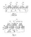
- FIG. 2illustrates a cross-sectional view of one embodiment of a stepped, non-planar NROM flash memory array of the present invention.
- the memory cellsare fabricated on a trenched substrate 200 with steps between the adjacent devices along the row of series connected transistors.
- the transistorsare not vertical structures but are conventional devices with conduction in channels that are parallel to the substrate surface. These devices achieve a density of 1F 2 /bit with multiple level cell storage.
- a portion of the array illustrated in FIG. 2is comprised of a column of transistors of which two 210 and 211 are discussed.
- An upper plane transistor 211is fabricated on a pillar on the substrate 200 .
- a lower plane transistor 210is fabricated in a trench of the substrate 200 .
- Source/drain regions 220 – 222are doped into the pillar/trench sidewalls. These regions 220 – 222 couple adjacent transistors of each plane together into columns (i.e., bitlines) of a NAND architecture memory array.
- the upper plane transistor 211uses source/drain regions 221 and 222 while the lower plane transistor 210 uses source/drain regions 220 and 221 . These two transistors 210 and 211 are coupled by the shared source/drain region 221 .
- Channel regionsexist at the top of each pillar and the bottom of each trench between the source/drain regions 220 – 222 .
- a channelforms between the source/drain regions 220 and 221 or 221 and 222 in the particular channel region of the operating transistor.
- the source/drain regions 220 – 222are n+ regions that are doped into a p-type substrate.
- the source/drain regions and substrate of the present inventionare not limited to any one conductivity type.
- a first dielectric layer 201is formed over the substrate 200 including both the pillars and the trenches and pillar/trench sidewalls.
- a silicon nitride layer 203is formed over the oxide layer 201 .
- This layer 203comprises the charge storage regions near the source/drain regions 220 – 222 for each particular transistor.
- each transistor 210 or 211has two charge storage regions 230 and 231 or 233 and 234 . Alternate embodiments may have different quantities of charge storage regions.
- a second dielectric layer 205is formed over the nitride layer 203 .
- Polysilicon control gates/wordlines 240 and 241are formed over the second dielectric layer 205 and substantially between each source/drain region 220 – 222 for either the pillar transistor 211 or the trench transistor 210 .
- the two dielectric layersare comprised of an oxide such that an oxide-nitride-oxide (ONO) gate insulator is formed. Alternate embodiments may use other dielectric materials.
- ONOoxide-nitride-oxide
- the wordlinescouple each memory array row of transistors.
- one wordline 240couples a row of the lower plane of transistors (i.e., the trenches).
- Another wordline 241couples a row of the upper plane of transistors (i.e., the pillars).
- the gate insulator and/or the intergate insulator between the nitride layer and the polysilicon wordlinescan be high-k dielectrics (i.e., dielectric constant greater than that of SiO 2 ), composite insulators, silicon oxide, or some other insulator.
- Silicon dioxide (SiO 2 )is an insulator with a relative dielectric constant of 3.9.
- a high-k gate insulatorrequires smaller write and erase voltages due to the reduced thickness layer between the control gate and the floating gate.
- These dielectric layersmay be formed by atomic layer deposition (ALD), evaporation, or some other fabrication technique.
- ALDis based on the sequential deposition of individual monolayers or fractions of a monolayer in a well-controlled manner. Gaseous precursors are introduced one at a time to the substrate surface and between the pulses the reactor is purged with an inert gas or evacuated.
- the precursoris saturatively chemisorbed at the substrate surface and during subsequent purging the precursor is removed from the reactor.
- another precursoris introduced on the substrate and the desired films growth reaction takes place. After that reaction, byproducts and the precursor excess are purged from the reactor.
- one ALD cyclecan be performed in less than one second in a properly designed flow-type reactor.
- the most commonly used oxygen source materials for ALDare water, hydrogen peroxide, and ozone. Alcohols, oxygen and nitrous oxide can also been used.
- ALDis well suited for deposition of high-k dielectrics such as AlO x , LaAlO 3 , HfAlO 3 , Pr 2 O 3 , Lanthanide-doped TiO x , HfSiON, Zr—Sn—Ti—O films using TiCl 4 or TiL 4 , ZrON, HfO 2 /Hf, ZrAl x O y , CrTiO 3 , and ZrTiO 4 .
- high-k dielectricssuch as AlO x , LaAlO 3 , HfAlO 3 , Pr 2 O 3 , Lanthanide-doped TiO x , HfSiON, Zr—Sn—Ti—O films using TiCl 4 or TiL 4 , ZrON, HfO 2 /Hf, ZrAl x O y , CrTiO 3 , and ZrTiO 4 .
- the dielectric layers of the present inventioncan also be formed by evaporation.
- Dielectric materials formed by evaporationcan include: TiO 2 , HfO 2 , CrTiO 3 , ZrO 2 , Y 2 O 3 , Gd 2 O 3 , PrO 2 , ZrO x N y , Y—Si—O, and LaAlO 3 .
- Very thin films of TiO 2can be fabricated with electron-gun evaporation from a high purity TiO 2 slug (e.g., 99.9999%) in a vacuum evaporator in the presence of an ion beam.
- an electron gunis centrally located toward the bottom of the chamber.
- a heat reflector and a heatersurround the substrate holder.
- Under the substrate holderis an ozonizer ring with many small holes directed to the wafer for uniform distribution of ozone that is needed to compensate for the loss of oxygen in the evaporated TiO 2 film.
- An ion gun with a fairly large diameter (3–4 in. in diameter)is located above the electron gun and argon gas is used to generate Ar ions to bombard the substrate surface uniformly during the film deposition to compact the growing TiO 2 film.
- a two-step processis used in fabricating a high purity HfO 2 film.
- This methodavoids the damage to the silicon surface by Ar ion bombardment, such as that encountered during Hf metal deposition using dc sputtering.
- a thin Hf filmis deposited by simple thermal evaporation. In one embodiment, this is by electron-beam evaporation using a high purity Hf metal slug (e.g., 99.9999%) at a low substrate temperature (e.g., 150°–200° C.). Since there is no plasma and ion bombardment of the substrate (as in the case of sputtering), the original atomically smooth surface of the silicon substrate is maintained.
- the second stepis oxidation to form the desired HfO 2 .
- the first step in the deposition of CoTi alloy filmis by thermal evaporation.
- the second stepis the low temperature oxidation of the CoTi film at 400° C. Electron beam deposition of the CoTi layer minimizes the effect of contamination during deposition.
- the CoTi films prepared from an electron gunpossess the highest purity because of the high-purity starting material. The purity of zone-refined starting metals can be as high as 99.999%. Higher purity can be obtained in deposited films because of further purification during evaporation.
- a two-step process in fabricating a high-purity ZrO 2 filmavoids the damage to the silicon surface by Ar ion bombardment.
- a thin Zr filmis deposited by simple thermal evaporation. In one embodiment, this is accomplished by electron beam evaporation using an ultra-high purity Zr metal slug (e.g., 99.9999%) at a low substrate temperature (e.g., 150°–200° C.). Since there is no plasma and ion bombardment of the substrate, the original atomically smooth surface of the silicon substrate is maintained.
- the second stepis the oxidation to form the desired ZrO 2 .
- Y 2 O 3 and Gd 2 O 3 filmsmay be accomplished with a two-step process.
- an electron gunprovides evaporation of high purity (e.g., 99.9999%) Y or Gd metal followed by low-temperature oxidation technology by microwave excitation in a Kr/O 2 mixed high-density plasma at 400° C.
- the method of the present inventionavoids damage to the silicon surface by Ar ion bombardment such as that encountered during Y or Gd metal deposition sputtering.
- a thin film of Y or Gdis deposited by thermal evaporation.
- an electron-beam evaporation techniqueis used with an ultra-high purity Y or Gd metal slug at a low substrate temperature (e.g., 150°–200° C.). Since there is no plasma or ion bombardment of the substrate, the original atomically smooth surface of the silicon substrate is maintained.
- the second stepis the oxidation to form the desired Y 2 O 3 or Gd 2 O 3 .
- the desired high purity of a PrO 2 filmcan be accomplished by depositing a thin film by simple thermal evaporation. In one embodiment, this is accomplished by an electron-beam evaporation technique using an ultra-high purity Pr metal slug at a low substrate temperature (e.g., 150°–200° C.). Since there is no plasma and ion bombardment of the substrate, the original atomically smooth surface of the silicon substrate is maintained.
- the second stepincludes the oxidation to form the desired PrO 2 .
- the nitridation of the ZrO 2 samplescomes after the low-temperature oxygen radical generated in high-density Krypton plasma.
- the next stepis the nitridation of the samples at temperatures >700° C. in a rapid thermal annealing setup. Typical heating time of several minutes may be necessary, depending on the sample geometry.
- a Y—Si—O filmmay be accomplished in one step by co-evaporation of the metal (Y) and silicon dioxide (SiO 2 ) without consuming the substrate Si.
- Ymetal
- SiO 2silicon dioxide
- yttriumis evaporated from one source, and SiO 2 is from another source.
- a small oxygen leakmay help reduce the oxygen deficiency in the film.
- the evaporation pressure ratio ratescan be adjusted easily to adjust the Y—Si—O ratio.
- the prior art fabrication of lanthanum aluminate (LaAlO 3 ) filmshas been achieved by evaporating single crystal pellets on Si substrates in a vacuum using an electron-beam gun.
- the evaporation technique of the present inventionuses a less expensive form of dry pellets of Al 2 O 3 and La 2 O 3 using two electron guns with two rate monitors. Each of the two rate monitors is set to control the composition.
- the composition of the filmcan be shifted toward the Al 2 O 3 or La 2 O 3 side depending upon the choice of dielectric constant.
- the waferis annealed ex situ in an electric furnace at 700° C. for ten minutes in N 2 ambience. In an alternate embodiment, the wafer is annealed at 800°–900° C. in RTA for ten to fifteen seconds in N 2 ambience.
- ALD and evaporation techniquesare for purposes of illustration only.
- the embodiments of the present inventionare not limited to any one dielectric material or dielectric fabrication technique.
- FIG. 3illustrates an embodiment for fabricating the non-planar NROM array of FIG. 2 .
- the substrate 300is etched to produce trenches 305 between the substrate pillars 308 and 309 .
- a doped oxideis deposited over the trenches 305 and pillars 308 and 309 . This oxide layer is directionally etched to leave the oxide only on the sidewalls 301 – 304 of the trenches.
- the sidewall oxideforms the source/drain regions 404 – 407 of the transistors as illustrated in FIG. 4 .
- the sidewall oxide layersare then removed.
- oxide intergate layer 403(ONO) as is described, for example, in “NROM: A Novel Localized Trapping, 2-Bit Nonvolatile Memory Cell”, by Boaz Eitan et al., IEEE Electron Device Letters, Vol. 21, No. 11, November 2000, pp. 543–545, IEEE Catalogue No. 0741-3106/00, or in “A True Single-Transistor Oxide-Nitride-Oxide EEPROM Device” by T. Y. Chan et al., IEEE Electron Device Letters, Vol. EDL-8, No. 3, March, 1987, pp. 93–95, IEEE Catalogue No. 0741-3106/87/0300-0093.
- the thin oxide, nitride, and oxide layerscombine to form the ONO gate insulator layer, such as is employed in SONOS devices.
- the gate insulatorhas a thickness of approximately 10 nanometers (nm).
- the gate insulatoris selected from the group of silicon dioxide (SiO 2 ) formed by wet oxidation, silicon oxynitride (SON), silicon rich oxide (SRO), and silicon rich aluminum oxide (Al 2 O 3 ).
- the gate insulatormay be selected from the group of silicon rich aluminum oxide insulators, silicon rich oxides with inclusions of nanoparticles of silicon, silicon oxide insulators with inclusions of nanoparticles of silicon carbide, and silicon oxycarbide insulators.
- the gate insulatorincludes a composite layer selected from the group of an oxide-aluminum oxide (Al 2 O 3 )-oxide composite layer, an oxide-silicon oxycarbide-oxide composite layer, and an oxide-nitride-aluminum oxide composite layer.
- the aluminum oxide top layerhas a higher dielectric constant so that this layer can be thicker in order to preclude tunneling to and from the control gate to the nitride storage layer.
- Alternate embodimentsuse other high dielectric constant insulators as the top layer.
- the gate insulatorincludes a composite layer, or a non-stoichiometric single layer of two or more materials selected from the group of silicon (Si), titanium (Ti), and tantalum (Ta).
- FIG. 5illustrates that a polysilicon wordline/control gate layer 501 – 503 is formed over the gate insulator. This process may be a directional, anisotropic deposition of polysilicon. Alternate embodiments may use other materials and/or processes for forming the wordlines/control gates.
- the structureshave been masked and a second set of trenches is etched perpendicular 601 to the original trenches. This separates the ONO structures of each cell, clears the sidewalls, and forms the pillars with source/drain regions along two of the sidewalls.
- the second set of trenchesis etched deeper into the substrate than the first set in order to affect a separation of the source/drain regions along the subsequent wordline/control gate.
- FIG. 6shows that each row of transistors in the upper plane is coupled together along the same wordline. Similarly, each row of the lower plane of transistors is coupled together along the same wordline.
- SONOS devicesare capable of storing more than one bit per gate.
- the hot carriersare injected into one side of the ONO layer, adjacent a source/drain region, to provide a high electrical field.
- chargemay be injected into the other side of the ONO layer.
- Hot majority charge carriersare not in thermal equilibrium with their environment. In other words, hot charge carriers represent a situation where a population of high kinetic energy charge carriers exist. Hot charge carriers may be electrons or holes.
- the stepped, non-planar NROM flash memory devices of the present inventioncan be programmed with tunnel injection using positive gate voltages with respect to the substrate/p-well.
- channel hot electron injectioncan be used in a programming operation. This is accomplished by applying a positive drain voltage (e.g., +6 to +9V) to a first source/drain region, a positive voltage to the control gate (e.g., +12V) and grounding the second source/drain region to create a hot electron injection into the gate insulator of the charge storage region.
- a positive drain voltagee.g., +6 to +9V
- the control gatee.g., +12V
- An alternate embodiment programming operationuses substrate enhanced hot electron injection (SEHE).
- SEHEsubstrate enhanced hot electron injection
- a negative substrate biasis applied to the p-type substrate. This bias increases the surface lateral field near a source/drain region thus increasing the number of hot electrons. The benefit of such an embodiment is that a lower drain voltage is required during programming operations.
- the negative substrate biasis in the range of 0V to ⁇ 3V. Alternate embodiments may use other voltage ranges.
- one embodimentuses tunneling with conventional negative gate voltages with respect to the substrate/p-well.
- the control gateis grounded, the drain connection is left floating and the source region has a positive voltage applied (e.g., +12V).
- Alternate embodiments for erase operationscan use other methods such as substrate enhanced band-to-band tunneling induced hot hole injection (SEBBHH) that are well known in the art.
- SEBBHHsubstrate enhanced band-to-band tunneling induced hot hole injection
- the present inventionis not limited to such a structure.
- the stepped, non-planar NROM arraycan be fabricated in a NOR architecture.
- the cellsare arranged in a matrix.
- the gates of each floating gate memory cell of the array matrixare connected by rows to wordlines and their drains are connected to column bitlines.
- the source of each floating gate memory cellis typically connected to a common source line. Still other embodiments can use other architectures.
- FIG. 7illustrates a functional block diagram of a memory device 700 that can incorporate the flash memory cells of the present invention.
- the memory device 700is coupled to a processor 710 .
- the processor 710may be a microprocessor or some other type of controlling circuitry.
- the memory device 700 and the processor 710form part of an electronic system 720 .
- the memory device 700has been simplified to focus on features of the memory that are helpful in understanding the present invention.
- the memory deviceincludes an array of NROM, flash memory cells 730 that can be comprised of the stepped, non-planar NROM cells illustrated previously.
- the memory array 730is arranged in banks of rows and columns.
- the control gates of each row of memory cellsis coupled with a wordline while the drain and source connections of the memory cells are coupled to bitlines.
- the connections of the cells to the bitlinesdetermines whether the array is a NAND architecture or a NOR architecture.
- An address buffer circuit 740is provided to latch address signals provided on address input connections A 0 -Ax 742 . Address signals are received and decoded by a row decoder 744 and a column decoder 746 to access the memory array 730 . It will be appreciated by those skilled in the art, with the benefit of the present description, that the number of address input connections depends on the density and architecture of the memory array 730 . That is, the number of addresses increases with both increased memory cell counts and increased bank and block counts.
- the memory device 700reads data in the memory array 730 by sensing voltage or current changes in the memory array columns using sense/buffer circuitry 750 .
- the sense/buffer circuitryin one embodiment, is coupled to read and latch a row of data from the memory array 730 .
- Data input and output buffer circuitry 760is included for bi-directional data communication over a plurality of data connections 762 with the controller 710 .
- Write circuitry 755is provided to write data to the memory array.
- Control circuitry 770decodes signals provided on control connections 772 from the processor 710 . These signals are used to control the operations on the memory array 730 , including data read, data write (program), and erase operations.
- the control circuitry 770may be a state machine, a sequencer, or some other type of controller.
- FIG. 7has been simplified to facilitate a basic understanding of the features of the memory. A more detailed understanding of internal circuitry and functions of NROM memories are known to those skilled in the art.
- the stepped, non-planar NROM flash memory cells of the present inventionprovide a high-density memory array with multiple level storage in a nitride layer.
- the densityin one embodiment, is 1F 2 /bit versus the typical 4F 2 /bit of the prior art conventional NAND flash memory structure.
- the memory cells of one array columni.e., bitline
- the cellsare coupled in series through the source/drain regions.
- the cellsare arranged in a matrix.
Landscapes
- Engineering & Computer Science (AREA)
- Microelectronics & Electronic Packaging (AREA)
- Non-Volatile Memory (AREA)
- Semiconductor Memories (AREA)
Abstract
Description
Claims (18)
Priority Applications (3)
| Application Number | Priority Date | Filing Date | Title |
|---|---|---|---|
| US10/899,906US7138681B2 (en) | 2004-07-27 | 2004-07-27 | High density stepped, non-planar nitride read only memory |
| US11/399,874US20060183271A1 (en) | 2004-07-27 | 2006-04-07 | High density stepped, non-planar nitride read only memory |
| US11/399,761US7427536B2 (en) | 2004-07-27 | 2006-04-07 | High density stepped, non-planar nitride read only memory |
Applications Claiming Priority (1)
| Application Number | Priority Date | Filing Date | Title |
|---|---|---|---|
| US10/899,906US7138681B2 (en) | 2004-07-27 | 2004-07-27 | High density stepped, non-planar nitride read only memory |
Related Child Applications (2)
| Application Number | Title | Priority Date | Filing Date |
|---|---|---|---|
| US11/399,761DivisionUS7427536B2 (en) | 2004-07-27 | 2006-04-07 | High density stepped, non-planar nitride read only memory |
| US11/399,874DivisionUS20060183271A1 (en) | 2004-07-27 | 2006-04-07 | High density stepped, non-planar nitride read only memory |
Publications (2)
| Publication Number | Publication Date |
|---|---|
| US20060023513A1 US20060023513A1 (en) | 2006-02-02 |
| US7138681B2true US7138681B2 (en) | 2006-11-21 |
Family
ID=35731978
Family Applications (3)
| Application Number | Title | Priority Date | Filing Date |
|---|---|---|---|
| US10/899,906Expired - LifetimeUS7138681B2 (en) | 2004-07-27 | 2004-07-27 | High density stepped, non-planar nitride read only memory |
| US11/399,874AbandonedUS20060183271A1 (en) | 2004-07-27 | 2006-04-07 | High density stepped, non-planar nitride read only memory |
| US11/399,761Expired - LifetimeUS7427536B2 (en) | 2004-07-27 | 2006-04-07 | High density stepped, non-planar nitride read only memory |
Family Applications After (2)
| Application Number | Title | Priority Date | Filing Date |
|---|---|---|---|
| US11/399,874AbandonedUS20060183271A1 (en) | 2004-07-27 | 2006-04-07 | High density stepped, non-planar nitride read only memory |
| US11/399,761Expired - LifetimeUS7427536B2 (en) | 2004-07-27 | 2006-04-07 | High density stepped, non-planar nitride read only memory |
Country Status (1)
| Country | Link |
|---|---|
| US (3) | US7138681B2 (en) |
Cited By (11)
| Publication number | Priority date | Publication date | Assignee | Title |
|---|---|---|---|---|
| US20050282334A1 (en)* | 2003-11-17 | 2005-12-22 | Micron Technology, Inc. | NROM flash memory devices on ultrathin silicon |
| US20060060910A1 (en)* | 2004-09-17 | 2006-03-23 | Ching-Sung Yang | Nonvolatile memory and manufacturing method and operating method thereof |
| US20060170038A1 (en)* | 2005-01-31 | 2006-08-03 | Wei-Zhe Wong | Non-volatile memory and manufacturing and operating method thereof |
| US20070008782A1 (en)* | 2005-07-06 | 2007-01-11 | Shankar Sinha | Method for programming a memory device |
| US20070159885A1 (en)* | 2004-12-30 | 2007-07-12 | Gorobets Sergey A | On-Chip Data Grouping and Alignment |
| US20070247924A1 (en)* | 2006-04-06 | 2007-10-25 | Wei Zheng | Methods for erasing memory devices and multi-level programming memory device |
| US20090218611A1 (en)* | 2004-08-03 | 2009-09-03 | Micron Technology, Inc. | High density stepped, non-planar flash memory |
| US7923381B2 (en) | 2002-12-04 | 2011-04-12 | Micron Technology, Inc. | Methods of forming electronic devices containing Zr-Sn-Ti-O films |
| US7972974B2 (en) | 2006-01-10 | 2011-07-05 | Micron Technology, Inc. | Gallium lanthanide oxide films |
| US8154066B2 (en) | 2004-08-31 | 2012-04-10 | Micron Technology, Inc. | Titanium aluminum oxide films |
| US8445952B2 (en) | 2002-12-04 | 2013-05-21 | Micron Technology, Inc. | Zr-Sn-Ti-O films |
Families Citing this family (34)
| Publication number | Priority date | Publication date | Assignee | Title |
|---|---|---|---|---|
| US6852167B2 (en)* | 2001-03-01 | 2005-02-08 | Micron Technology, Inc. | Methods, systems, and apparatus for uniform chemical-vapor depositions |
| US8026161B2 (en) | 2001-08-30 | 2011-09-27 | Micron Technology, Inc. | Highly reliable amorphous high-K gate oxide ZrO2 |
| US6844203B2 (en)* | 2001-08-30 | 2005-01-18 | Micron Technology, Inc. | Gate oxides, and methods of forming |
| US7160577B2 (en) | 2002-05-02 | 2007-01-09 | Micron Technology, Inc. | Methods for atomic-layer deposition of aluminum oxides in integrated circuits |
| US7589029B2 (en) | 2002-05-02 | 2009-09-15 | Micron Technology, Inc. | Atomic layer deposition and conversion |
| US7045430B2 (en)* | 2002-05-02 | 2006-05-16 | Micron Technology Inc. | Atomic layer-deposited LaAlO3 films for gate dielectrics |
| US7205218B2 (en)* | 2002-06-05 | 2007-04-17 | Micron Technology, Inc. | Method including forming gate dielectrics having multiple lanthanide oxide layers |
| US7135421B2 (en) | 2002-06-05 | 2006-11-14 | Micron Technology, Inc. | Atomic layer-deposited hafnium aluminum oxide |
| US6790791B2 (en)* | 2002-08-15 | 2004-09-14 | Micron Technology, Inc. | Lanthanide doped TiOx dielectric films |
| US7199023B2 (en)* | 2002-08-28 | 2007-04-03 | Micron Technology, Inc. | Atomic layer deposited HfSiON dielectric films wherein each precursor is independendently pulsed |
| US7192892B2 (en) | 2003-03-04 | 2007-03-20 | Micron Technology, Inc. | Atomic layer deposited dielectric layers |
| US7135369B2 (en)* | 2003-03-31 | 2006-11-14 | Micron Technology, Inc. | Atomic layer deposited ZrAlxOy dielectric layers including Zr4AlO9 |
| US7192824B2 (en)* | 2003-06-24 | 2007-03-20 | Micron Technology, Inc. | Lanthanide oxide / hafnium oxide dielectric layers |
| US7138681B2 (en)* | 2004-07-27 | 2006-11-21 | Micron Technology, Inc. | High density stepped, non-planar nitride read only memory |
| US7081421B2 (en) | 2004-08-26 | 2006-07-25 | Micron Technology, Inc. | Lanthanide oxide dielectric layer |
| US7494939B2 (en) | 2004-08-31 | 2009-02-24 | Micron Technology, Inc. | Methods for forming a lanthanum-metal oxide dielectric layer |
| US7235501B2 (en) | 2004-12-13 | 2007-06-26 | Micron Technology, Inc. | Lanthanum hafnium oxide dielectrics |
| US7560395B2 (en) | 2005-01-05 | 2009-07-14 | Micron Technology, Inc. | Atomic layer deposited hafnium tantalum oxide dielectrics |
| US7374964B2 (en)* | 2005-02-10 | 2008-05-20 | Micron Technology, Inc. | Atomic layer deposition of CeO2/Al2O3 films as gate dielectrics |
| US7687409B2 (en) | 2005-03-29 | 2010-03-30 | Micron Technology, Inc. | Atomic layer deposited titanium silicon oxide films |
| US7365027B2 (en) | 2005-03-29 | 2008-04-29 | Micron Technology, Inc. | ALD of amorphous lanthanide doped TiOx films |
| US7662729B2 (en) | 2005-04-28 | 2010-02-16 | Micron Technology, Inc. | Atomic layer deposition of a ruthenium layer to a lanthanide oxide dielectric layer |
| US7927948B2 (en) | 2005-07-20 | 2011-04-19 | Micron Technology, Inc. | Devices with nanocrystals and methods of formation |
| US7709402B2 (en) | 2006-02-16 | 2010-05-04 | Micron Technology, Inc. | Conductive layers for hafnium silicon oxynitride films |
| JP2008053270A (en)* | 2006-08-22 | 2008-03-06 | Nec Electronics Corp | Semiconductor memory device and manufacturing method thereof |
| US7605030B2 (en) | 2006-08-31 | 2009-10-20 | Micron Technology, Inc. | Hafnium tantalum oxynitride high-k dielectric and metal gates |
| TW200818402A (en)* | 2006-10-03 | 2008-04-16 | Powerchip Semiconductor Corp | Non-volatile memory, fabricating method and operating method thereof |
| US7760547B2 (en)* | 2007-09-25 | 2010-07-20 | Sandisk Corporation | Offset non-volatile storage |
| JP5349903B2 (en)* | 2008-02-28 | 2013-11-20 | ルネサスエレクトロニクス株式会社 | Semiconductor device manufacturing method and semiconductor device |
| US8586962B2 (en) | 2008-10-06 | 2013-11-19 | Samsung Electronics Co., Ltd. | Cross point memory arrays, methods of manufacturing the same, masters for imprint processes, and methods of manufacturing masters |
| US8105884B2 (en)* | 2008-10-06 | 2012-01-31 | Samsung Electronics Co., Ltd. | Cross point memory arrays, methods of manufacturing the same, masters for imprint processes, and methods of manufacturing masters |
| SG11201603374PA (en)* | 2013-10-29 | 2016-05-30 | Allegiance Corp | Hydrophilic/hydrophobic aqueous polymer emulsions and products and methods relating thereto |
| US9449978B2 (en)* | 2014-01-06 | 2016-09-20 | Micron Technology, Inc. | Semiconductor devices including a recessed access device and methods of forming same |
| JP6578172B2 (en)* | 2015-09-18 | 2019-09-18 | ルネサスエレクトロニクス株式会社 | Semiconductor device |
Citations (5)
| Publication number | Priority date | Publication date | Assignee | Title |
|---|---|---|---|---|
| US6555870B1 (en)* | 1999-06-29 | 2003-04-29 | Kabushiki Kaisha Toshiba | Nonvolatile semiconductor memory device and method for producing same |
| US6583479B1 (en) | 2000-10-16 | 2003-06-24 | Advanced Micro Devices, Inc. | Sidewall NROM and method of manufacture thereof for non-volatile memory cells |
| US6627945B1 (en) | 2002-07-03 | 2003-09-30 | Advanced Micro Devices, Inc. | Memory device and method of making |
| US6670246B1 (en) | 2002-12-17 | 2003-12-30 | Nanya Technology Corporation | Method for forming a vertical nitride read-only memory |
| US6720217B2 (en) | 2002-07-18 | 2004-04-13 | Hynix Semiconductor Inc. | Method of manufacturing flash memory device using trench device isolation process |
Family Cites Families (14)
| Publication number | Priority date | Publication date | Assignee | Title |
|---|---|---|---|---|
| US5045490A (en)* | 1990-01-23 | 1991-09-03 | Texas Instruments Incorporated | Method of making a pleated floating gate trench EPROM |
| JPH05102436A (en)* | 1991-10-09 | 1993-04-23 | Ricoh Co Ltd | Semiconductor memory device and manufacture thereof |
| US5511020A (en)* | 1993-11-23 | 1996-04-23 | Monolithic System Technology, Inc. | Pseudo-nonvolatile memory incorporating data refresh operation |
| US5780890A (en)* | 1994-12-26 | 1998-07-14 | Nippon Steel Corporation | Nonvolatile semiconductor memory device and a method of writing data in the same |
| JPH09162313A (en)* | 1995-12-12 | 1997-06-20 | Rohm Co Ltd | Nonvolatile semiconductor memory device and method of using the same |
| US5929477A (en)* | 1997-01-22 | 1999-07-27 | International Business Machines Corporation | Self-aligned diffused source vertical transistors with stack capacitors in a 4F-square memory cell array |
| JP3948292B2 (en)* | 2002-02-01 | 2007-07-25 | 株式会社日立製作所 | Semiconductor memory device and manufacturing method thereof |
| US6853587B2 (en)* | 2002-06-21 | 2005-02-08 | Micron Technology, Inc. | Vertical NROM having a storage density of 1 bit per 1F2 |
| US7202523B2 (en)* | 2003-11-17 | 2007-04-10 | Micron Technology, Inc. | NROM flash memory devices on ultrathin silicon |
| US7050330B2 (en)* | 2003-12-16 | 2006-05-23 | Micron Technology, Inc. | Multi-state NROM device |
| US7241654B2 (en)* | 2003-12-17 | 2007-07-10 | Micron Technology, Inc. | Vertical NROM NAND flash memory array |
| US7190616B2 (en)* | 2004-07-19 | 2007-03-13 | Micron Technology, Inc. | In-service reconfigurable DRAM and flash memory device |
| US7138681B2 (en)* | 2004-07-27 | 2006-11-21 | Micron Technology, Inc. | High density stepped, non-planar nitride read only memory |
| TWI262595B (en)* | 2005-08-08 | 2006-09-21 | Powerchip Semiconductor Corp | Non-volatile memory and fabricating method thereof |
- 2004
- 2004-07-27USUS10/899,906patent/US7138681B2/ennot_activeExpired - Lifetime
- 2006
- 2006-04-07USUS11/399,874patent/US20060183271A1/ennot_activeAbandoned
- 2006-04-07USUS11/399,761patent/US7427536B2/ennot_activeExpired - Lifetime
Patent Citations (5)
| Publication number | Priority date | Publication date | Assignee | Title |
|---|---|---|---|---|
| US6555870B1 (en)* | 1999-06-29 | 2003-04-29 | Kabushiki Kaisha Toshiba | Nonvolatile semiconductor memory device and method for producing same |
| US6583479B1 (en) | 2000-10-16 | 2003-06-24 | Advanced Micro Devices, Inc. | Sidewall NROM and method of manufacture thereof for non-volatile memory cells |
| US6627945B1 (en) | 2002-07-03 | 2003-09-30 | Advanced Micro Devices, Inc. | Memory device and method of making |
| US6720217B2 (en) | 2002-07-18 | 2004-04-13 | Hynix Semiconductor Inc. | Method of manufacturing flash memory device using trench device isolation process |
| US6670246B1 (en) | 2002-12-17 | 2003-12-30 | Nanya Technology Corporation | Method for forming a vertical nitride read-only memory |
Cited By (24)
| Publication number | Priority date | Publication date | Assignee | Title |
|---|---|---|---|---|
| US8445952B2 (en) | 2002-12-04 | 2013-05-21 | Micron Technology, Inc. | Zr-Sn-Ti-O films |
| US7923381B2 (en) | 2002-12-04 | 2011-04-12 | Micron Technology, Inc. | Methods of forming electronic devices containing Zr-Sn-Ti-O films |
| US7378316B2 (en) | 2003-11-17 | 2008-05-27 | Micron Technology, Inc. | Method for fabricating semiconductor vertical NROM memory cells |
| US8183625B2 (en) | 2003-11-17 | 2012-05-22 | Micron Technology, Inc. | NROM flash memory devices on ultrathin silicon |
| US7915669B2 (en) | 2003-11-17 | 2011-03-29 | Micron Technology, Inc. | NROM flash memory devices on ultrathin silicon |
| US7768058B2 (en) | 2003-11-17 | 2010-08-03 | Micron Technology, Inc. | NROM flash memory devices on ultrathin silicon |
| US7276413B2 (en)* | 2003-11-17 | 2007-10-02 | Micron Technology, Inc. | NROM flash memory devices on ultrathin silicon |
| US20050282334A1 (en)* | 2003-11-17 | 2005-12-22 | Micron Technology, Inc. | NROM flash memory devices on ultrathin silicon |
| US20090218611A1 (en)* | 2004-08-03 | 2009-09-03 | Micron Technology, Inc. | High density stepped, non-planar flash memory |
| US8017988B2 (en)* | 2004-08-03 | 2011-09-13 | Micron Technology, Inc. | High density stepped, non-planar flash memory |
| US8154066B2 (en) | 2004-08-31 | 2012-04-10 | Micron Technology, Inc. | Titanium aluminum oxide films |
| US8541276B2 (en) | 2004-08-31 | 2013-09-24 | Micron Technology, Inc. | Methods of forming an insulating metal oxide |
| US7462902B2 (en)* | 2004-09-17 | 2008-12-09 | Powerchip Semiconductor Corp. | Nonvolatile memory |
| US20090042350A1 (en)* | 2004-09-17 | 2009-02-12 | Powerchip Semiconductor Corp. | Manufacturing method of nonvolatile memory |
| US20060060910A1 (en)* | 2004-09-17 | 2006-03-23 | Ching-Sung Yang | Nonvolatile memory and manufacturing method and operating method thereof |
| US20070159885A1 (en)* | 2004-12-30 | 2007-07-12 | Gorobets Sergey A | On-Chip Data Grouping and Alignment |
| US7391078B2 (en)* | 2005-01-31 | 2008-06-24 | Powerchip Semiconductor Corp. | Non-volatile memory and manufacturing and operating method thereof |
| US20060170038A1 (en)* | 2005-01-31 | 2006-08-03 | Wei-Zhe Wong | Non-volatile memory and manufacturing and operating method thereof |
| US20070008782A1 (en)* | 2005-07-06 | 2007-01-11 | Shankar Sinha | Method for programming a memory device |
| US7269067B2 (en)* | 2005-07-06 | 2007-09-11 | Spansion Llc | Programming a memory device |
| US7972974B2 (en) | 2006-01-10 | 2011-07-05 | Micron Technology, Inc. | Gallium lanthanide oxide films |
| US9129961B2 (en) | 2006-01-10 | 2015-09-08 | Micron Technology, Inc. | Gallium lathanide oxide films |
| US9583334B2 (en) | 2006-01-10 | 2017-02-28 | Micron Technology, Inc. | Gallium lanthanide oxide films |
| US20070247924A1 (en)* | 2006-04-06 | 2007-10-25 | Wei Zheng | Methods for erasing memory devices and multi-level programming memory device |
Also Published As
| Publication number | Publication date |
|---|---|
| US7427536B2 (en) | 2008-09-23 |
| US20060183271A1 (en) | 2006-08-17 |
| US20060023513A1 (en) | 2006-02-02 |
| US20060180876A1 (en) | 2006-08-17 |
Similar Documents
| Publication | Publication Date | Title |
|---|---|---|
| US7138681B2 (en) | High density stepped, non-planar nitride read only memory | |
| US7544989B2 (en) | High density stepped, non-planar flash memory | |
| US7164168B2 (en) | Non-planar flash memory having shielding between floating gates | |
| US7339228B2 (en) | Non-planar flash memory array with shielded floating gates on silicon mesas | |
| US7157769B2 (en) | Flash memory having a high-permittivity tunnel dielectric | |
| US7221018B2 (en) | NROM flash memory with a high-permittivity gate dielectric | |
| US20060273370A1 (en) | NROM flash memory with vertical transistors and surrounding gates | |
| US7601593B2 (en) | Flash memory with metal-insulator-metal tunneling program and erase | |
| US20050212065A1 (en) | NROM memory device with a high-permittivity gate dielectric formed by the low temperature oxidation of metals | |
| US7198999B2 (en) | Flash memory device having a graded composition, high dielectric constant gate insulator | |
| US7855114B2 (en) | High K stack for non-volatile memory | |
| JP2009049409A (en) | Nonvolatile memory device and manufacturing method thereof |
Legal Events
| Date | Code | Title | Description |
|---|---|---|---|
| AS | Assignment | Owner name:MICRON TECHNOLOGY, INC., IDAHO Free format text:ASSIGNMENT OF ASSIGNORS INTEREST;ASSIGNORS:FORBES, LEONARD;AHN, KIE Y.;REEL/FRAME:015631/0348;SIGNING DATES FROM 20040716 TO 20040719 | |
| FEPP | Fee payment procedure | Free format text:PAYOR NUMBER ASSIGNED (ORIGINAL EVENT CODE: ASPN); ENTITY STATUS OF PATENT OWNER: LARGE ENTITY | |
| STCF | Information on status: patent grant | Free format text:PATENTED CASE | |
| FPAY | Fee payment | Year of fee payment:4 | |
| FPAY | Fee payment | Year of fee payment:8 | |
| AS | Assignment | Owner name:U.S. BANK NATIONAL ASSOCIATION, AS COLLATERAL AGENT, CALIFORNIA Free format text:SECURITY INTEREST;ASSIGNOR:MICRON TECHNOLOGY, INC.;REEL/FRAME:038669/0001 Effective date:20160426 Owner name:U.S. BANK NATIONAL ASSOCIATION, AS COLLATERAL AGEN Free format text:SECURITY INTEREST;ASSIGNOR:MICRON TECHNOLOGY, INC.;REEL/FRAME:038669/0001 Effective date:20160426 | |
| AS | Assignment | Owner name:MORGAN STANLEY SENIOR FUNDING, INC., AS COLLATERAL AGENT, MARYLAND Free format text:PATENT SECURITY AGREEMENT;ASSIGNOR:MICRON TECHNOLOGY, INC.;REEL/FRAME:038954/0001 Effective date:20160426 Owner name:MORGAN STANLEY SENIOR FUNDING, INC., AS COLLATERAL Free format text:PATENT SECURITY AGREEMENT;ASSIGNOR:MICRON TECHNOLOGY, INC.;REEL/FRAME:038954/0001 Effective date:20160426 | |
| AS | Assignment | Owner name:U.S. BANK NATIONAL ASSOCIATION, AS COLLATERAL AGENT, CALIFORNIA Free format text:CORRECTIVE ASSIGNMENT TO CORRECT THE REPLACE ERRONEOUSLY FILED PATENT #7358718 WITH THE CORRECT PATENT #7358178 PREVIOUSLY RECORDED ON REEL 038669 FRAME 0001. ASSIGNOR(S) HEREBY CONFIRMS THE SECURITY INTEREST;ASSIGNOR:MICRON TECHNOLOGY, INC.;REEL/FRAME:043079/0001 Effective date:20160426 Owner name:U.S. BANK NATIONAL ASSOCIATION, AS COLLATERAL AGEN Free format text:CORRECTIVE ASSIGNMENT TO CORRECT THE REPLACE ERRONEOUSLY FILED PATENT #7358718 WITH THE CORRECT PATENT #7358178 PREVIOUSLY RECORDED ON REEL 038669 FRAME 0001. ASSIGNOR(S) HEREBY CONFIRMS THE SECURITY INTEREST;ASSIGNOR:MICRON TECHNOLOGY, INC.;REEL/FRAME:043079/0001 Effective date:20160426 | |
| MAFP | Maintenance fee payment | Free format text:PAYMENT OF MAINTENANCE FEE, 12TH YEAR, LARGE ENTITY (ORIGINAL EVENT CODE: M1553) Year of fee payment:12 | |
| AS | Assignment | Owner name:JPMORGAN CHASE BANK, N.A., AS COLLATERAL AGENT, ILLINOIS Free format text:SECURITY INTEREST;ASSIGNORS:MICRON TECHNOLOGY, INC.;MICRON SEMICONDUCTOR PRODUCTS, INC.;REEL/FRAME:047540/0001 Effective date:20180703 Owner name:JPMORGAN CHASE BANK, N.A., AS COLLATERAL AGENT, IL Free format text:SECURITY INTEREST;ASSIGNORS:MICRON TECHNOLOGY, INC.;MICRON SEMICONDUCTOR PRODUCTS, INC.;REEL/FRAME:047540/0001 Effective date:20180703 | |
| AS | Assignment | Owner name:MICRON TECHNOLOGY, INC., IDAHO Free format text:RELEASE BY SECURED PARTY;ASSIGNOR:U.S. BANK NATIONAL ASSOCIATION, AS COLLATERAL AGENT;REEL/FRAME:047243/0001 Effective date:20180629 | |
| AS | Assignment | Owner name:MICRON TECHNOLOGY, INC., IDAHO Free format text:RELEASE BY SECURED PARTY;ASSIGNOR:MORGAN STANLEY SENIOR FUNDING, INC., AS COLLATERAL AGENT;REEL/FRAME:050937/0001 Effective date:20190731 | |
| AS | Assignment | Owner name:MICRON SEMICONDUCTOR PRODUCTS, INC., IDAHO Free format text:RELEASE BY SECURED PARTY;ASSIGNOR:JPMORGAN CHASE BANK, N.A., AS COLLATERAL AGENT;REEL/FRAME:051028/0001 Effective date:20190731 Owner name:MICRON TECHNOLOGY, INC., IDAHO Free format text:RELEASE BY SECURED PARTY;ASSIGNOR:JPMORGAN CHASE BANK, N.A., AS COLLATERAL AGENT;REEL/FRAME:051028/0001 Effective date:20190731 |