US7138659B2 - LED assembly with vented circuit board - Google Patents
LED assembly with vented circuit boardDownload PDFInfo
- Publication number
- US7138659B2 US7138659B2US10/847,343US84734304AUS7138659B2US 7138659 B2US7138659 B2US 7138659B2US 84734304 AUS84734304 AUS 84734304AUS 7138659 B2US7138659 B2US 7138659B2
- Authority
- US
- United States
- Prior art keywords
- led
- circuit board
- conductive layer
- leds
- layer
- Prior art date
- Legal status (The legal status is an assumption and is not a legal conclusion. Google has not performed a legal analysis and makes no representation as to the accuracy of the status listed.)
- Expired - Fee Related
Links
Images


Classifications
- G—PHYSICS
- G09—EDUCATION; CRYPTOGRAPHY; DISPLAY; ADVERTISING; SEALS
- G09F—DISPLAYING; ADVERTISING; SIGNS; LABELS OR NAME-PLATES; SEALS
- G09F9/00—Indicating arrangements for variable information in which the information is built-up on a support by selection or combination of individual elements
- G09F9/30—Indicating arrangements for variable information in which the information is built-up on a support by selection or combination of individual elements in which the desired character or characters are formed by combining individual elements
- G09F9/33—Indicating arrangements for variable information in which the information is built-up on a support by selection or combination of individual elements in which the desired character or characters are formed by combining individual elements being semiconductor devices, e.g. diodes
- G—PHYSICS
- G09—EDUCATION; CRYPTOGRAPHY; DISPLAY; ADVERTISING; SEALS
- G09F—DISPLAYING; ADVERTISING; SIGNS; LABELS OR NAME-PLATES; SEALS
- G09F13/00—Illuminated signs; Luminous advertising
- G09F13/20—Illuminated signs; Luminous advertising with luminescent surfaces or parts
- H—ELECTRICITY
- H05—ELECTRIC TECHNIQUES NOT OTHERWISE PROVIDED FOR
- H05K—PRINTED CIRCUITS; CASINGS OR CONSTRUCTIONAL DETAILS OF ELECTRIC APPARATUS; MANUFACTURE OF ASSEMBLAGES OF ELECTRICAL COMPONENTS
- H05K1/00—Printed circuits
- H05K1/02—Details
- H05K1/0201—Thermal arrangements, e.g. for cooling, heating or preventing overheating
- H05K1/0203—Cooling of mounted components
- H05K1/0209—External configuration of printed circuit board adapted for heat dissipation, e.g. lay-out of conductors, coatings
- H—ELECTRICITY
- H05—ELECTRIC TECHNIQUES NOT OTHERWISE PROVIDED FOR
- H05K—PRINTED CIRCUITS; CASINGS OR CONSTRUCTIONAL DETAILS OF ELECTRIC APPARATUS; MANUFACTURE OF ASSEMBLAGES OF ELECTRICAL COMPONENTS
- H05K2201/00—Indexing scheme relating to printed circuits covered by H05K1/00
- H05K2201/06—Thermal details
- H05K2201/064—Fluid cooling, e.g. by integral pipes
- H—ELECTRICITY
- H05—ELECTRIC TECHNIQUES NOT OTHERWISE PROVIDED FOR
- H05K—PRINTED CIRCUITS; CASINGS OR CONSTRUCTIONAL DETAILS OF ELECTRIC APPARATUS; MANUFACTURE OF ASSEMBLAGES OF ELECTRICAL COMPONENTS
- H05K2201/00—Indexing scheme relating to printed circuits covered by H05K1/00
- H05K2201/09—Shape and layout
- H05K2201/09818—Shape or layout details not covered by a single group of H05K2201/09009 - H05K2201/09809
- H05K2201/0989—Coating free areas, e.g. areas other than pads or lands free of solder resist
- H—ELECTRICITY
- H05—ELECTRIC TECHNIQUES NOT OTHERWISE PROVIDED FOR
- H05K—PRINTED CIRCUITS; CASINGS OR CONSTRUCTIONAL DETAILS OF ELECTRIC APPARATUS; MANUFACTURE OF ASSEMBLAGES OF ELECTRICAL COMPONENTS
- H05K2201/00—Indexing scheme relating to printed circuits covered by H05K1/00
- H05K2201/10—Details of components or other objects attached to or integrated in a printed circuit board
- H05K2201/10007—Types of components
- H05K2201/10106—Light emitting diode [LED]
- H—ELECTRICITY
- H05—ELECTRIC TECHNIQUES NOT OTHERWISE PROVIDED FOR
- H05K—PRINTED CIRCUITS; CASINGS OR CONSTRUCTIONAL DETAILS OF ELECTRIC APPARATUS; MANUFACTURE OF ASSEMBLAGES OF ELECTRICAL COMPONENTS
- H05K2201/00—Indexing scheme relating to printed circuits covered by H05K1/00
- H05K2201/10—Details of components or other objects attached to or integrated in a printed circuit board
- H05K2201/10431—Details of mounted components
- H05K2201/1056—Metal over component, i.e. metal plate over component mounted on or embedded in PCB
- H—ELECTRICITY
- H05—ELECTRIC TECHNIQUES NOT OTHERWISE PROVIDED FOR
- H05K—PRINTED CIRCUITS; CASINGS OR CONSTRUCTIONAL DETAILS OF ELECTRIC APPARATUS; MANUFACTURE OF ASSEMBLAGES OF ELECTRICAL COMPONENTS
- H05K2203/00—Indexing scheme relating to apparatus or processes for manufacturing printed circuits covered by H05K3/00
- H05K2203/08—Treatments involving gases
- H05K2203/081—Blowing of gas, e.g. for cooling or for providing heat during solder reflowing
- H—ELECTRICITY
- H05—ELECTRIC TECHNIQUES NOT OTHERWISE PROVIDED FOR
- H05K—PRINTED CIRCUITS; CASINGS OR CONSTRUCTIONAL DETAILS OF ELECTRIC APPARATUS; MANUFACTURE OF ASSEMBLAGES OF ELECTRICAL COMPONENTS
- H05K2203/00—Indexing scheme relating to apparatus or processes for manufacturing printed circuits covered by H05K3/00
- H05K2203/11—Treatments characterised by their effect, e.g. heating, cooling, roughening
- H05K2203/1178—Means for venting or for letting gases escape
- H—ELECTRICITY
- H05—ELECTRIC TECHNIQUES NOT OTHERWISE PROVIDED FOR
- H05K—PRINTED CIRCUITS; CASINGS OR CONSTRUCTIONAL DETAILS OF ELECTRIC APPARATUS; MANUFACTURE OF ASSEMBLAGES OF ELECTRICAL COMPONENTS
- H05K3/00—Apparatus or processes for manufacturing printed circuits
- H05K3/22—Secondary treatment of printed circuits
- H05K3/28—Applying non-metallic protective coatings
Definitions
- the inventionrelates to lighting units using light emitting diodes (LEDs). More particularly, the invention relates to a light emitting diode assembly with a vented circuit board.
- LEDslight emitting diodes
- LEDSLight-emitting diodes
- display assemblies having LEDsgenerate heat as electric current flows through the devices. The heat must be dissipated or removed to prevent overheating. Cooling a display assembly is important in order to preserve its functionality and efficiency. Furthermore, display assemblies when used in outdoor environments may be exposed to wind forces that affect loading on the assemblies.
- PCT publication WO2004019657One approach for cooling an LED display assembly is shown in PCT publication WO2004019657. The publication generally shows a coolant fluid which cools LEDs using a mesh design.
- a printed circuit board assemblyincludes a plurality of LEDs disposed in a grid pattern at junctions in which the junctions are interconnected by adjacent bridges defining air vents.
- a plurality of ventsenables air to pass through the printed circuit board assembly, thus reducing wind resistance and promoting cooling.
- a printed circuit board assemblyin another variation, includes a plurality of LED modules, each LED module being disposed at a corresponding junction, the junctions being connected to bridges in which adjacent bridges define air vents for allowing air to pass through.
- the bridges and junctionsinclude a multilayer substrate having an insulating layer and a thermal cooling layer in thermal communication with the LED modules.
- the insulating layermay include a plurality of fluid openings configured for fluid convective heat transfer with the thermal cooling layer.
- a printed circuit board assemblyincludes a plurality of LED modules and a multilayer substrate.
- the multilayered substratemay have an external insulating layer and a thermal cooling layer in thermal communication with the LED modules.
- the external insulating layerincludes a plurality of openings which exposes the thermal cooling layer for fluid convective heat transfer.
- a printed circuit board assemblyincludes a plurality of LEDs having a dome.
- the LEDsmay be disposed in a grid pattern at junctions being interconnected by bridges defining air vents.
- the bridgesinclude a substrate for activating the LEDs and the substrate includes a front side including the LEDs and an opposing a rear side. Aerodynamic members configured to reduce air pressure are disposed on the second side of the substrate corresponding to location of the junctions. In this way, wind loading may be reduced for multiple directions.
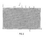
- FIG. 1illustrates a perspective view of a printed circuit board assembly according to one or more aspects of the present invention.
- FIG. 2illustrates a frontal elevation view of the printed circuit board assembly of FIG. 1 .
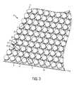
- FIG. 3illustrates an enlarged view of the printed circuit board assembly of FIG. 1 with LED modules.
- FIG. 4illustrates an enlarged view of a printed circuit board assembly similar to FIG. 3 , with the LED modules according to one or more aspects of the present invention.
- FIG. 5illustrates a first rear perspective view of an LED module according to one or more aspects of the present invention.
- FIG. 6illustrates a front perspective view of the LED module of FIG. 5 according to one or more aspects of the present invention.
- FIG. 7illustrates a second rear perspective view of a LED module according to one or more aspects of the present invention.
- FIG. 8illustrates a perspective view of an alternative embodiment of a printed circuit board assembly according to one or more aspects of the present invention.
- FIG. 9illustrates a schematic diagram of one possible decoder-conductor arrangement for energizing components of a LED module according to one or more aspects of the present invention.
- FIG. 10illustrates an enlarged view of the PCB assembly of FIG. 1 with a first heat dissipation feature according to one or more aspects of the present invention.
- FIG. 11illustrates an enlarged view of the PCB assembly of FIG. 1 with a second heat dissipation feature according to one or more aspects of the present invention.
- FIG. 12illustrates an enlarged view of the PCB assembly of FIG. 1 with a third heat dissipation feature according to one or more aspects of the present invention.
- FIG. 13illustrates a partial schematic section view of the printed circuit board assembly taken along line 13 — 13 of FIG. 10 .
- FIG. 14illustrates a schematic diagram of a conductor-LED module arrangement according to one or more aspects of the present invention.
- FIG. 15illustrates a partial schematic section view of an alternative multilayer substrate arrangement according to one or more aspects of the present invention.
- FIG. 16illustrates a partial schematic section diagram of an alternative multilayer substrate arrangement according to one or more aspects of the present invention.
- FIG. 17illustrates a partial schematic diagram of an alternative PCB assembly according to one or more aspects of the present invention.
- FIG. 18illustrates a partial schematic diagram of a PCB assembly with roughness members according to one or more aspects of the present invention.
- FIGS. 1–4illustrate an embodiment of a printed circuit board (PCB) assembly 2 including an array or grid pattern of light emitting diode (LED) modules 4 mounted thereon.
- the LED modules 4are disposed at intersecting junctions 5 of the PCB assembly 2 in a generally perpendicular X-direction and Y-direction based on a Cartesian coordinate system.
- the junctions 5are interconnected by a plurality of bridges 17 defining vents 22 , which may be drilled or routed in the printed circuit board.
- printed circuit boardis used for ease of reference, it should be understood that other types of circuit boards other than printed boards may be used, and such boards are intended to be encompassed within the term “printed circuit board” or PCB. Examples may include embedded wires, ribbon cables, or similar structures.
- FIGS. 5–7illustrate an embodiment of an LED module 4 according to one or more aspects of the present invention.
- LED module 4may include one or more LEDs 6 a–d disposed within the interior cavity of a removable translucent dome or cap 8 .
- the capis optional and may not be required in all applications.
- the LED module 4may have more or fewer LEDs depending on the acceptability for the intended use.
- an LED modulemay consist of a single LED mechanically attached by, for example, soldering to the circuit board.
- the dome 8may be formed of several alternative materials, such as a translucent plastic or glass. Various materials may be selected for atmospheric environments based on the intended use. An appropriate material and thickness characteristics enables the dome 8 to protect the LED 6 a–d against physical impingement from flying projectiles in the air or rain, and may help in reducing aerodynamic drag on the assembly. Dome 8 can be optically neutral to preserve the optical characteristics of the LED 6 a–d , such as field-of-view focusing. Alternatively, dome 8 may also have optical properties that enhance those of the LED 6 a–d , such as lowering the side leakage. The material may also protect the LEDs 6 a–d from UV damage that may discolor the optical material or other internal components.
- the UV protectionhelps to mitigate brightness reduction of the LEDs 6 a–d over time due to exposure to external UV wavelengths.
- the dome 8may be removably mounted via a friction-fit engagement to a base member 10 .
- dome 8may be mounted to the base member 10 in other ways, such as in a snap-fit or threaded engagement.
- the removable arrangement of the dome 8provides access for field or bench-level maintenance, such as replacement or upgrade to the LED 6 a–d or other components of LED module 4 .
- LED modulesmay be removed from the PCB assembly for maintenance and the like.
- the LED modulemay be attached to the board by a hinge or similar mechanism such that it can be opened without being removed.
- base member 10includes extension members or protrusions 12 that may be utilized for mounting the LED module 4 to the PCB assembly 2 .
- the extension members 12may provide a partial heat transfer path for cooling the LED module 4 in conjunction with PCB 2 assembly substrates.
- the base member 10may be composed of a number of alternative materials, including copper, aluminum, or a mixture of metal particulates suspended in a plastic material, carbon fibers or other well known material that provides thermal conductivity without electrical connection.
- the base member 10may have an annular or circular shape.
- base member 10may be formed in several shape configurations depending on the intended use of the LED module 4 .
- a peripheral surface of the base member 10may retain a sealing member 14 .
- the sealing member 14may be configured to prevent debris and other external environmental components from entering into the interior cavity of the LED module 4 formed between the dome 8 and base member 10 .
- the sealing configuration with the dome 8also provides protection of the LEDs 6 a–d against environmental conditions, such as temperature, humidity, salt, acid rain and the like.
- the sealing member 14can be formed in several shapes and mounted to the base member 10 using conventional methods and techniques.
- the sealing member 14can be formed as an annular ring, such as an O-ring. Further, the sealing member 14 may be composed of a resilient material, such as rubber or a synthetic rubber. For mounting arrangements, the sealing member 14 may be adhesively bonded to the base member 10 . Alternatively, the sealing member 14 can provide compression forces for a friction fit engagement with the base member 10 .
- each LED 6 a–dincludes two electrical leads 16 physically connected to respective electrical conductors.
- Lead material and lengthmay be selected to maximize thermal connection between LED and circuit board for heat dissipation, as discussed in more detail below.
- leads 16are shown, the LED module may have other alternative configurations.
- the LED modulemay be surface mounted or a direct-on-die arrangement on the PCB assembly substrate. In such a surface mount configuration, the leads are connected to electrical conductors or traces.
- a single LEDmay be placed at each junction, and may be selectively illuminated by energizing a corresponding X-wire conductor and Y-wire conductor, such that the LED at the junction of the X-wire conductor and Y-wire conductor causes the LED to be illuminated.
- more than one LEDmay be affixed to each junction, such that a single X-wire conductor and Y-wire conductor when energized cause all of the LEDs at the junction to be illuminated.
- a plurality of X-wire conductors and a plurality of Y-wire conductorsoverlap at the junction, such that more than one pair of conductors is available to selectively illuminate one or more LEDs at the junction.
- Drivers of various typesmay be used in association with the LEDS, such that signaling is provided on one set of conductors while power is provided by means of other conductors.
- multiple LEDs at the junctionmay be selectively energized by means of a decoder that decodes signals on corresponding X-wire conductors and Y-wire conductors such that a larger number of LEDs can be selectively illuminated using a smaller number of conductors.
- the LED module 4may include a decoder unit 18 which may be configured for control of energizing or de-energizing each respective LED 6 a–d through MOSFET gating or other means. Each decoder unit 18 may be responsive to computer readable commands intended for controlling each LED 6 a–d . Alternatively, each LED 6 a–d within the module 4 may be energized simultaneously for increased illumination and brightness characteristics depending on the intended application. For example, applications that may utilize the PCB assembly 2 could be a vehicular or aircraft traffic signage; large screen video displays; and computerized video billboards and the like.
- each decoder unit 18may have six leads for various logic control functions with a computer and the like.
- the LED module 4may include a heat resistor 20 disposed between the LEDs 6 a–d .
- the heat resistor 20may be energized when defogging or deicing of the dome 8 or other internal components is needed.
- one of the decoder units 18may be configured to control the heat resistor 20 .
- a separate electrical conductor connected to a switchmay control operation of the heat resistor 20 .
- the PCB assembly at the junctions 5may include electrical conductors 11 a–c and 13 a–b .
- the conductorsmay be provided in a two-by-three array for selectively energizing the intended LED 6 a–d within the LED module 4 . More or fewer conductors may be used depending on the desired configuration.
- Conductor 11 ccan be used for providing power or other signals to the decoder unit 18 .
- the decoder unit 18may be connected to the electrical conductors 11 a–c and 13 a–b in a conventional manner to enable control of LEDs 6 a–d.
- FIG. 14illustrates one possible arrangement of conductors and an LED module 4 at the junction 5 without a decoder unit controlling the LED module.
- the PCB assembly 2may be constructed in a multilayered arrangement in which the different conductive layers include conductors in the X-direction and the Y-direction, separated by an insulating layer.
- FIG. 14shows a two-by-two array of conductors x 1 , x 2 and conductors y 1 , y 2 disposed on different conductive layers for energizing LEDs 6 a–d . In operation, each LED 6 a–d may be energized in a number of different configurations.
- LED 6 amay be energized with conductor x 1 and conductor y 1 ; LED 6 b may be illuminated with conductor x 1 and conductor y 2 . LED 6 c can be illuminated with conductor x 2 and conductor y 2 . LED 6 d may be energized by conductor x 2 and conductor y 1 . Nonetheless, all the conductors x 1 - 2 and y 1 - 2 may be used to illuminate all the LEDs 6 a–d for increased brightness. While LED modules with four LEDs have been shown, a single LED may be disposed at the junctions and operate with or without a decoder unit. In this approach, the LEDs 6 a–d can be addressable by the conductor arrangement.
- FIGS. 10–12illustrate alternative arrangements of the PCB assembly 2 for providing heat dissipation for cooling the LED modules.
- the PCB assembly 2includes thermodynamic cooling features and aerodynamic features, such as a plurality of air vents 22 .
- the vents 22enable air to pass through the PCB assembly 2 to reduce wind pressure on the PCB assembly and may assist with heat dissipation.
- This vent configurationadvantageously enables the PCB assembly to be implemented in high environments and prevents excessive wind loading.
- the air vents 22are configured for removing the heat generated by the LED modules 4 and other electrical components.
- the cooling exchange provided by the vents 22reduces localized hot spots in the PCB assembly 2 .
- the junctions 5are connected by bridges 17 in which the air vents 22 are defined between the bridge and junctions.
- the multilayer substrateincludes the bridges 17 .
- the air vents 22are devoid of material between four adjacent junctions 5 and bridges 17 .
- the air vents 22are generally shaped as a square configuration. Nonetheless, other shapes are possible.
- the bridges 17have a width smaller than the diameter of the junctions 5 .
- a ratio of the width of the bridges to the diameter of the junctionsis less than one. This is one way of controlling the size of the vents by controlling the width of the bridges 17 .
- this configurationreduces wind pressure on the PCB assembly 2 . In an exposed environment, the air may flow through the vents 22 for passive cooling of the LED modules 4 by way of natural convection.
- fluidic cooling of the PCB assembly 2can be implemented by providing a cooling fluid of sufficient velocity and a volume to flow over the LED modules 4 and through the fluid vents 22 .
- the cooling fluidmay flow in a direction parallel to a plane formed by the X-direction and Y-direction.
- the cooling fluid with sufficient volume and velocitymay flow primarily through the air vents 22 by being directed generally perpendicular of the plane of the PCB assembly 2 .
- a cooling fluidmay be a gas, such as ambient air, drawn external to the PCB assembly 2 in an enclosed arrangement.
- the cooling fluidcould be recirculated air after heat is removed via an air conditioning device (not shown). The heat is removed from LED modules 4 by convection.
- FIG. 8shows an alternative PCB assembly 2 ′ with large size vents 26 to promote additional air passing through PCB assembly and additional cooling of the LED modules 4 .
- the size of the vents 26are controlled by the width of the bridges 6 ′ and the length. This configuration enables more air to pass through the vents 26 for reducing wind loading and subsequent stress on the structure.
- PCB assembly 2 ′has similar components of PCB assembly 2 .
- PCB assembly 2 ′may be used with other aspects of heat dissipation and aerodynamic features of the present invention.
- the size of the ventsis many times the size of each LED module, thus providing a minimal cross-section to wind.
- FIG. 13shows a section view of the PCB assembly 2 taken along line 13 – 13 of FIG. 10 .
- the PCB assembly 2may be constructed in a multilayered arrangement comprising a plurality of layers 2 a–g .
- layers 2 a , 2 c , 2 e and 2 gmay be composed of a dielectric insulator.
- a thermal conductive layer 2 bmay be disposed between the outer layer 2 a and a dielectric insulator layer 2 c .
- a first electrical conductive layer 2 dmay be disposed between dielectric insulator layers 2 c and 2 e .
- a second electrical conductive layer 2 fmay be disposed between insulator layers 2 e and 2 g .
- the substratemay have more or fewer layers and other arrangements of the layers are possible.
- the sidewalls 7may also be the outer layer 2 a of the multilayer substrate.
- the PCB assembly 2may be manufactured using conventional multilayered conductor techniques.
- the leads 16 of LEDs 6 amay extend through holes in the dielectric layer 2 a , thermal conductive layer 2 b , and dielectric layers 2 c , 2 e to the conductive layers 2 d and 2 f .
- each lead 16may be same length and the holes may include metal deposits through conventional manufacturing methods to enable electrical current to flow from the conductor layers to each lead 16 .
- the thermal conductive layer 2 bmay the thermally insolated from the leads 16 and the holes.
- the dielectric outer layer 2 a of the PCB assembly 2may have a plurality of fluid openings 24 for exposing a thermal conductive layer 2 b for air communication to increase the effective convective contact area to allow heat dissipation of the LED modules 4 .
- the openings 24are devoid of a dielectric material so as to form pathways in which a flowing cooling fluid, such as air, may contact the thermal conductive layer 2 b to receive heat. In such an arrangement, the air may enter the opening 24 and the air is prevented from flow through the PCB by the thermal conductive layer 2 b .
- the openings 24may have a circular shape. Nevertheless, the openings 24 may have other shapes depending on a desired cooling performance with respect to the convective contact area. For example, the shapes may be square, rectangular, triangular, oval, and the like.
- the openings 24may be in the form of the slots in the dielectric outer layer 2 a .
- the openings 24may be disposed on the top surface of the PCB assembly substrate.
- the openings 24may be located on a sidewall 7 in the vents 22 of the PCB assembly substrate.
- the sidewall 7 arrangement of the opening 24 in combination with a cooling fluid, such as air, flowing through the vents 22provides an incremental heat transfer advantage by enabling increased fluid exchange with the thermal conductive layer 2 b .
- the material of the thermal layer 2 bmay have an appropriate heat transfer coefficient based on the heat generating characteristics of the LED modules 4 .
- the thermal conductive layer 2 bcan be composed of a number of alternative materials, including a copper, aluminum, or a mixture of metal particulates suspended in a plastic material.
- the thermal coefficient of thermal expansion of the conductive layer and dielectric layerswould be matched to take into account any thermal induced mechanical stress.
- small holesmay extend all the way through the substrate in the bridge 17 so air can pass through the bridge. The small holes may be placed proximate to the LED modules to close proximity to the location of heat generation. In this way, there is the possibility of obtaining improved heat dissipation.
- the thermal conductive layer 2 bmay be physically connected to the base member 10 , in particular to the protrusions 12 of the LED module 4 .
- the base member 10may serve as a heat sink with respect to the LEDs 6 a–d .
- the thermal conductive layer 2 bmay be a lower temperature than the LED module 4 .
- a resultant thermal temperature differentialenables the heat generated by the LED 6 a–d to be transferred to the base member 10 and to the thermal conductive layer 2 b .
- a thermoelectric cooling module(not shown) may be used to lower the temperature of the thermal conductive layer 2 b . This creates an enhanced heat sink performance for the thermal layer.
- the thermoelectric cooling modulemay be powered with the conductors from layers 2 d and 2 f.
- FIG. 16illustrates a section view of an alternative multilayer substrate 50 with an LED 32 .
- LED 32includes a cathode lead 52 and an anode lead 54 for receiving electrical power.
- the lead 52 of LED 32may be connected to trace layer 50 b .
- the lead 54 of LED 32may extend to trace layer 50 d .
- the thermally conductive layer(s) 50 a and 50 cmay be disposed in close proximity to the trace/layer 50 b which is thermally and electrically connected to the cathode lead 52 of the LED.
- either side of the trace layer 50 bcan be sandwiched by the thermal layer(s) 50 a and 50 c to provide maximum thermal dissipation and/or heat sinking.
- Thermal layer 50 cmay be disposed between the trace layer 50 b and layer 50 d .
- a single thermal conductive layermay simultaneously provide heat transfer benefits for both trace layers. This configuration may also reduce the thickness of the substrate 50 .
- Multilayer substrate 50may be used with PCB assembly 2 shown in FIGS. 1–4 and the air vents 22 for maximum heat conduction.
- the thermal conductive layer 50 a and 50 cmay be composed of various materials which provide thermal conduction yet high electrical resistance, including polymeric, polymeric blends, or carbon fibers.
- FIG. 12illustrates an alternative heat dissipation arrangement including an outer exposed layer 30 which may serve both electrical and thermal conductive functions.
- the convective contact areais increased for cooling the LED module or LEDs in the cooling configuration.
- the layer 30may serve as an electrical conductor for the LED module or LEDs.
- FIG. 15illustrates a section view of an alternative multilayer substrate 34 with an LED 32 .
- Multilayer substrate 34includes an exposed upper layer 34 a that serves as both an electrical conductor and a thermal conductor for heat dissipation.
- Upper layer 34 amay include one or more conductors in the X-direction.
- a bottom electrical conductive layer 34 cmay include one or more conductors in the Y-direction.
- a dielectric insulating layer 34 bmay be disposed between the layer 34 a and layer 34 c .
- LED 32includes two lead 36 , 38 for receiving electrical power. The lead 36 of LED 32 may be connected to upper layer 34 a .
- the lead 38 of LED 32may extend through holes in layer 34 a , and dielectric layer 34 b to the conductive layer 34 c . While a single LED is shown, the inventive aspects can be practiced with multiple LEDs or LED modules. Multilayer substrate 34 may be used with PCB assembly 2 shown in FIGS. 1–4 and the heat dissipation vents 22 . In this embodiment, electrically and thermally conductive layer 34 a assists in dissipating heat from LED 32 .
- layer 34 amay comprise a thermally conductive layer that has poor electrical conducting qualities, thus helping to dissipate heat while acting as an electrical insulator.
- Layer 34 bcould then be used as the electrical path to LED 32 , and another layer 34 d (not shown) would act as the other electrical conductor.
- LED leads 36 and 38would be connected to layers 34 b and 34 d (not shown) for electrical connectivity.
- FIG. 17illustrates a partial schematic diagram of an alternative PCB assembly 60 with a two-sided aerodynamic configuration which provides a benefit of reducing wind pressure.
- the substrate 62has a front side 64 and rear side 66 .
- the LED module 32may mounted on the front side 64 and the LED module 32 may include a dome 8 .
- the rear side of the PCB assembly 60may include an aerodynamic member 68 for reducing wind pressure.
- the PCB assembly 60includes air vents (not shown) for enabling air to pass through the PCB. Air flowing towards the LED module 32 of dome 8 can reduce air pressure, and air flowing in an opposite direction also has reduced resistance with respect to the structure.
- the aerodynamic membermay comprise various shapes such as a hemispherical shape or a nose cone shape.
- the bridge 17may include a plurality of roughness members 70 on the surface of the multilayer substrate.
- the roughness members 70protrude from the surface of the substrate.
- the members 70can have a variety of shapes, such as hemispherical and the like. These roughness members 70 may be provided to promote small air turbulence to reduce the boundary layer for reducing the insulating effects of the air and promote increased heat transfer from the thermal layer to the air.
- roughness members 70may increase the interaction of the air with the thermal layer to improved passive cooling.
- One of ordinary skill in the airmay embodiment computational fluid mechanics and the like for specific dimensional characteristics.
Landscapes
- Engineering & Computer Science (AREA)
- Physics & Mathematics (AREA)
- General Physics & Mathematics (AREA)
- Theoretical Computer Science (AREA)
- Microelectronics & Electronic Packaging (AREA)
- Arrangement Of Elements, Cooling, Sealing, Or The Like Of Lighting Devices (AREA)
- Led Device Packages (AREA)
- Cooling Or The Like Of Semiconductors Or Solid State Devices (AREA)
Abstract
Description
Claims (6)
Priority Applications (6)
| Application Number | Priority Date | Filing Date | Title |
|---|---|---|---|
| US10/847,343US7138659B2 (en) | 2004-05-18 | 2004-05-18 | LED assembly with vented circuit board |
| PCT/US2005/009302WO2005119633A1 (en) | 2004-05-18 | 2005-03-17 | Led assembly with vented circuit board |
| US11/538,779US20070086188A1 (en) | 2004-05-18 | 2006-10-04 | LED Assembly with Vented Circuit Board |
| US11/538,790US20070086189A1 (en) | 2004-05-18 | 2006-10-04 | LED Assembly with Vented Circuit Board |
| US11/538,786US7315049B2 (en) | 2004-05-18 | 2006-10-04 | LED assembly with vented circuit board |
| US11/538,769US20070086187A1 (en) | 2004-05-18 | 2006-10-04 | LED Assembly with Vented Circuit Board |
Applications Claiming Priority (1)
| Application Number | Priority Date | Filing Date | Title |
|---|---|---|---|
| US10/847,343US7138659B2 (en) | 2004-05-18 | 2004-05-18 | LED assembly with vented circuit board |
Related Child Applications (4)
| Application Number | Title | Priority Date | Filing Date |
|---|---|---|---|
| US11/538,769DivisionUS20070086187A1 (en) | 2004-05-18 | 2006-10-04 | LED Assembly with Vented Circuit Board |
| US11/538,786DivisionUS7315049B2 (en) | 2004-05-18 | 2006-10-04 | LED assembly with vented circuit board |
| US11/538,779DivisionUS20070086188A1 (en) | 2004-05-18 | 2006-10-04 | LED Assembly with Vented Circuit Board |
| US11/538,790DivisionUS20070086189A1 (en) | 2004-05-18 | 2006-10-04 | LED Assembly with Vented Circuit Board |
Publications (2)
| Publication Number | Publication Date |
|---|---|
| US20050258446A1 US20050258446A1 (en) | 2005-11-24 |
| US7138659B2true US7138659B2 (en) | 2006-11-21 |
Family
ID=34963444
Family Applications (5)
| Application Number | Title | Priority Date | Filing Date |
|---|---|---|---|
| US10/847,343Expired - Fee RelatedUS7138659B2 (en) | 2004-05-18 | 2004-05-18 | LED assembly with vented circuit board |
| US11/538,786Expired - LifetimeUS7315049B2 (en) | 2004-05-18 | 2006-10-04 | LED assembly with vented circuit board |
| US11/538,769AbandonedUS20070086187A1 (en) | 2004-05-18 | 2006-10-04 | LED Assembly with Vented Circuit Board |
| US11/538,779AbandonedUS20070086188A1 (en) | 2004-05-18 | 2006-10-04 | LED Assembly with Vented Circuit Board |
| US11/538,790AbandonedUS20070086189A1 (en) | 2004-05-18 | 2006-10-04 | LED Assembly with Vented Circuit Board |
Family Applications After (4)
| Application Number | Title | Priority Date | Filing Date |
|---|---|---|---|
| US11/538,786Expired - LifetimeUS7315049B2 (en) | 2004-05-18 | 2006-10-04 | LED assembly with vented circuit board |
| US11/538,769AbandonedUS20070086187A1 (en) | 2004-05-18 | 2006-10-04 | LED Assembly with Vented Circuit Board |
| US11/538,779AbandonedUS20070086188A1 (en) | 2004-05-18 | 2006-10-04 | LED Assembly with Vented Circuit Board |
| US11/538,790AbandonedUS20070086189A1 (en) | 2004-05-18 | 2006-10-04 | LED Assembly with Vented Circuit Board |
Country Status (2)
| Country | Link |
|---|---|
| US (5) | US7138659B2 (en) |
| WO (1) | WO2005119633A1 (en) |
Cited By (26)
| Publication number | Priority date | Publication date | Assignee | Title |
|---|---|---|---|---|
| US20060238327A1 (en)* | 2005-04-21 | 2006-10-26 | C.R.F. Societa Consortile Per Azioni | Transparent LED display |
| US20070032843A1 (en)* | 2005-08-03 | 2007-02-08 | Fu-Yu Hsu | Phototherapy apparatus |
| US20070081328A1 (en)* | 2005-08-15 | 2007-04-12 | Chi-Chin Yu | Illuminating device for plants |
| US20070252161A1 (en)* | 2006-03-31 | 2007-11-01 | 3M Innovative Properties Company | Led mounting structures |
| US20080137308A1 (en)* | 2006-12-11 | 2008-06-12 | Magna International Inc. | Thermal Management system and method for semiconductor lighting systems |
| US20080298033A1 (en)* | 2007-06-01 | 2008-12-04 | Smith Roy A | Power supply platform and electronic component |
| US20090073713A1 (en)* | 2007-09-07 | 2009-03-19 | Glovatsky Andrew Z | LED Multidimensional Printed Wiring Board Using Standoff Boards |
| US20090225545A1 (en)* | 2008-03-10 | 2009-09-10 | Seiko Epson Corporation | Light source device and light source packaging method |
| US20100039815A1 (en)* | 2008-08-13 | 2010-02-18 | Advanced Analog Technology, Inc. | Led apparatus and the pcb thereof |
| WO2010068485A1 (en)* | 2008-11-25 | 2010-06-17 | Robertson Transformer Co. | Method and apparatus for using thermionic devices to recover energy from light sources and other energy conversion devices |
| US20110044000A1 (en)* | 2008-02-06 | 2011-02-24 | Light Prescriptions Innovators, Llc. | Transparent heat-spreader for optoelectronic applications |
| CN102810287A (en)* | 2012-08-10 | 2012-12-05 | 深圳市易事达电子有限公司 | Led display screen |
| US8824125B1 (en) | 2013-03-16 | 2014-09-02 | ADTI Media, LLC | Modular installation and conversion kit for electronic sign structure and method of using same |
| US8929083B2 (en) | 2013-03-16 | 2015-01-06 | ADIT Media, LLC | Compound structural frame and method of using same for efficient retrofitting |
| US20150138786A1 (en)* | 2013-08-19 | 2015-05-21 | CLEDOS green tech Limited | Structures for LED Light Bulbs |
| US9047791B2 (en) | 2013-03-16 | 2015-06-02 | Adti Media, Llc. | Sign construction with sectional sign assemblies and installation kit and method of using same |
| US9666105B2 (en) | 2013-03-16 | 2017-05-30 | ADTI Media, LLC | Sign construction with modular wire harness arrangements and methods of using same for backside to frontside power and data distribution schemes |
| US9761157B2 (en) | 2013-03-16 | 2017-09-12 | Adti Media Llc | Customized sectional sign assembly kit and method of using kit for construction and installation of same |
| US9852666B2 (en) | 2013-03-16 | 2017-12-26 | Adti Media Llc | Full height sectional sign assembly and installation kit and method of using same |
| US10061553B2 (en) | 2013-12-31 | 2018-08-28 | Ultravision Technologies, Llc | Power and data communication arrangement between panels |
| US10248372B2 (en) | 2013-12-31 | 2019-04-02 | Ultravision Technologies, Llc | Modular display panels |
| US10373535B2 (en) | 2013-12-31 | 2019-08-06 | Ultravision Technologies, Llc | Modular display panel |
| US10706770B2 (en) | 2014-07-16 | 2020-07-07 | Ultravision Technologies, Llc | Display system having module display panel with circuitry for bidirectional communication |
| US10891881B2 (en) | 2012-07-30 | 2021-01-12 | Ultravision Technologies, Llc | Lighting assembly with LEDs and optical elements |
| US11404243B1 (en)* | 2014-01-27 | 2022-08-02 | Mochii, Inc. | Microscopy |
| US12437965B1 (en)* | 2022-08-01 | 2025-10-07 | Mochil, Inc. | Charged-particle beam microscope with differential vacuum pressures |
Families Citing this family (77)
| Publication number | Priority date | Publication date | Assignee | Title |
|---|---|---|---|---|
| DE10245892A1 (en)* | 2002-09-30 | 2004-05-13 | Siemens Ag | Illumination device for backlighting an image display device |
| US20060017658A1 (en)* | 2004-03-15 | 2006-01-26 | Onscreen Technologies, Inc. | Rapid dispatch emergency signs |
| US8188503B2 (en)* | 2004-05-10 | 2012-05-29 | Permlight Products, Inc. | Cuttable illuminated panel |
| US7138659B2 (en) | 2004-05-18 | 2006-11-21 | Onscreen Technologies, Inc. | LED assembly with vented circuit board |
| US8733966B2 (en) | 2004-08-20 | 2014-05-27 | Mag Instrument, Inc. | LED flashlight |
| DE102005013762C5 (en)* | 2005-03-22 | 2012-12-20 | Sew-Eurodrive Gmbh & Co. Kg | Electronic device and method for determining the temperature of a power semiconductor |
| CA2617314A1 (en)* | 2005-04-05 | 2006-10-12 | Tir Technology Lp | Mounting assembly for optoelectronic devices |
| DE102005033005A1 (en)* | 2005-07-14 | 2007-01-18 | Osram Opto Semiconductors Gmbh | Optoelectronic chip |
| US7986112B2 (en)* | 2005-09-15 | 2011-07-26 | Mag Instrument, Inc. | Thermally self-stabilizing LED module |
| US20100177519A1 (en)* | 2006-01-23 | 2010-07-15 | Schlitz Daniel J | Electro-hydrodynamic gas flow led cooling system |
| TWI333580B (en)* | 2006-02-08 | 2010-11-21 | Chimei Innolux Corp | Backlight module and liquid crystal display using the same |
| US7806574B2 (en) | 2006-04-16 | 2010-10-05 | Albeo Technologies, Inc. | Thermal management of LED-based lighting systems |
| US8425085B2 (en) | 2006-04-16 | 2013-04-23 | Albeo Technologies, Inc. | Thermal management of LED-based lighting systems |
| US20070247851A1 (en) | 2006-04-21 | 2007-10-25 | Villard Russel G | Light Emitting Diode Lighting Package With Improved Heat Sink |
| WO2007130358A2 (en) | 2006-05-02 | 2007-11-15 | Superbulbs, Inc. | Plastic led bulb |
| WO2007130357A2 (en) | 2006-05-02 | 2007-11-15 | Superbulbs, Inc. | Method of light dispersion and preferential scattering of certain wavelengths of light for light-emitting diodes and bulbs constructed therefrom |
| CA2645231A1 (en) | 2006-05-02 | 2007-11-15 | Superbulbs, Inc. | Heat removal design for led bulbs |
| US7686469B2 (en) | 2006-09-30 | 2010-03-30 | Ruud Lighting, Inc. | LED lighting fixture |
| US20090086491A1 (en) | 2007-09-28 | 2009-04-02 | Ruud Lighting, Inc. | Aerodynamic LED Floodlight Fixture |
| US9441824B2 (en) | 2008-04-04 | 2016-09-13 | Cree, Inc. | LED light fixture with heat-dissipation-related high light output |
| US9028087B2 (en) | 2006-09-30 | 2015-05-12 | Cree, Inc. | LED light fixture |
| US20080123340A1 (en)* | 2006-11-27 | 2008-05-29 | Mcclellan Thomas | Light device having LED illumination and electronic circuit board in an enclosure |
| KR101396658B1 (en)* | 2006-12-29 | 2014-05-19 | 엘지디스플레이 주식회사 | Light Cube and Flat Light Unit and Liquid Crystal Display Device including the same |
| US20080212332A1 (en)* | 2007-03-01 | 2008-09-04 | Medinis David M | LED cooling system |
| KR20080086245A (en)* | 2007-03-22 | 2008-09-25 | 삼성전자주식회사 | Backlight assembly and liquid crystal display including the same |
| US20100219734A1 (en)* | 2007-06-08 | 2010-09-02 | Superbulbs, Inc. | Apparatus for cooling leds in a bulb |
| KR101405972B1 (en)* | 2007-07-02 | 2014-06-12 | 엘지전자 주식회사 | broadcasting receiver and method of processing broadcast signal |
| US8439528B2 (en) | 2007-10-03 | 2013-05-14 | Switch Bulb Company, Inc. | Glass LED light bulbs |
| JP2011501464A (en) | 2007-10-24 | 2011-01-06 | テオス・インコーポレイテッド | Diffuser for LED light source |
| DE102008038857A1 (en)* | 2008-03-31 | 2009-10-01 | Osram Opto Semiconductors Gmbh | lighting device |
| USRE49637E1 (en) | 2008-04-04 | 2023-08-29 | Ideal Industries Lighting Llc | Systems and methods for high output, high color quality light |
| EP2110803A1 (en)* | 2008-04-17 | 2009-10-21 | Dmitrijs Volohovs | Method for demonstrating video images and apparatus therefor |
| US9022612B2 (en)* | 2008-08-07 | 2015-05-05 | Mag Instrument, Inc. | LED module |
| US20100097780A1 (en)* | 2008-10-21 | 2010-04-22 | John Bryan Beatenbough | Refrigerated led illumination system |
| US20100226139A1 (en) | 2008-12-05 | 2010-09-09 | Permlight Products, Inc. | Led-based light engine |
| US9247598B2 (en) | 2009-01-16 | 2016-01-26 | Mag Instrument, Inc. | Portable lighting devices |
| US9677746B2 (en)* | 2009-06-18 | 2017-06-13 | Rafael M. Ramirez | Power delivery system for HID, LED, or fluorescent track lighting |
| TW201105893A (en)* | 2009-08-05 | 2011-02-16 | Leotek Electronics Corp | LED lamp module and LED lamp |
| USD621804S1 (en)* | 2009-08-07 | 2010-08-17 | Hon Hai Precision Industry Co., Ltd. | PCB for arranging LED lights |
| TW201105897A (en)* | 2009-08-12 | 2011-02-16 | Leotek Electronics Corp | LED lamp and dissipating heat method of LED lamp |
| KR101011379B1 (en)* | 2010-03-24 | 2011-01-28 | 주식회사 에이팩 | Luminaires using light emitting diodes |
| US8534880B1 (en)* | 2010-04-12 | 2013-09-17 | Analog Technologies Corp. | Solid state lighting system |
| CN102221134A (en)* | 2010-04-14 | 2011-10-19 | 富准精密工业(深圳)有限公司 | Lighting device |
| CN101866586B (en)* | 2010-04-23 | 2015-07-08 | 北京中庆微数字设备开发有限公司 | Flexible display screen mounting structure and flexible display screen |
| WO2012029002A1 (en)* | 2010-08-31 | 2012-03-08 | Koninklijke Philips Electronics N.V. | Led-based lighting units with substantially sealed leds |
| US8226274B2 (en) | 2011-03-01 | 2012-07-24 | Switch Bulb Company, Inc. | Liquid displacer in LED bulbs |
| JP5948813B2 (en)* | 2011-05-09 | 2016-07-06 | ソニー株式会社 | Illumination device and display device |
| US20130016510A1 (en)* | 2011-07-12 | 2013-01-17 | Sanders Brian C | Modular led illumination apparatus |
| US8591069B2 (en) | 2011-09-21 | 2013-11-26 | Switch Bulb Company, Inc. | LED light bulb with controlled color distribution using quantum dots |
| US8587019B2 (en)* | 2011-10-11 | 2013-11-19 | Ledengin, Inc. | Grooved plate for improved solder bonding |
| US20130100670A1 (en)* | 2011-10-20 | 2013-04-25 | Osram Sylvania Inc. | Lighting system with a heat sink having plurality of heat conduits |
| US10215378B2 (en)* | 2012-04-13 | 2019-02-26 | Cree, Inc. | Light fixture |
| CN102737554A (en)* | 2012-06-29 | 2012-10-17 | 北京金立翔艺彩科技股份有限公司 | Supporting substrate manufacturing method and light emitting diode (LED) display device |
| CN103582282B (en)* | 2012-07-25 | 2018-05-18 | 欧司朗股份有限公司 | Circuit board, electronic module and light emitting module including the circuit board |
| DE202012009187U1 (en)* | 2012-09-25 | 2012-11-09 | Frank Freitag | Lighting surface device |
| WO2014153271A2 (en)* | 2013-03-16 | 2014-09-25 | ADTI Media, LLC | Sectional sign assembly and installation kit and method of using same |
| US20140292198A1 (en)* | 2013-03-28 | 2014-10-02 | American Machine Vision Llc | Multiple application led illumination system |
| USD761745S1 (en)* | 2013-06-28 | 2016-07-19 | Sumitomo Electric Industries, Ltd. | Semiconductor device |
| CN103700325A (en)* | 2014-01-07 | 2014-04-02 | 罗盛 | Stereo-structure indoor transparent LED (light emitting diode) display screen |
| US9714746B2 (en) | 2014-04-29 | 2017-07-25 | Cooledge Lighting Inc. | Modular LED lighting systems |
| USD740239S1 (en)* | 2014-05-07 | 2015-10-06 | Bejan Esau Amini | LED illumination tile |
| US9755110B1 (en)* | 2016-07-27 | 2017-09-05 | Sharp Laboratories Of America, Inc. | Substrate with topological features for steering fluidic assembly LED disks |
| JP6476856B2 (en)* | 2014-12-26 | 2019-03-06 | 日亜化学工業株式会社 | Display device, display |
| WO2017060187A1 (en)* | 2015-10-09 | 2017-04-13 | Philips Lighting Holding B.V. | Lighting device |
| US10228117B2 (en) | 2015-11-06 | 2019-03-12 | Honeywell International Inc. | Air mixing methodology and system to reduce the temperature of LEDs of a photocatalytic reactor |
| CN105405367A (en)* | 2015-12-14 | 2016-03-16 | 深圳市大族元亨光电股份有限公司 | Grid-type LED display module |
| US11274823B1 (en) | 2016-03-02 | 2022-03-15 | Cooledge Lighting, Inc. | Lighting systems incorporating connections for signal and power transmission |
| US10746358B1 (en) | 2016-03-02 | 2020-08-18 | Cooledge Lighting Inc. | Lighting systems incorporating connections for signal and power transmission |
| US10344954B1 (en) | 2016-03-02 | 2019-07-09 | Cooledge Lighting Inc. | Lighting systems incorporating connections for signal and power transmission |
| CA3106393A1 (en)* | 2018-07-13 | 2020-01-16 | 10644137 Canada Inc. | High-performance high-power led lighting systems and methods thereof |
| JP7360246B2 (en)* | 2019-03-14 | 2023-10-12 | 株式会社ジャパンディスプレイ | display device |
| WO2020227497A1 (en)* | 2019-05-09 | 2020-11-12 | Jeffway Jr Robert W | Two-sided illuminating printed circuit board assembly and illuminating device using the same |
| WO2021170194A1 (en)* | 2020-02-26 | 2021-09-02 | LED iBond International A/S | Air transport unit |
| US11160319B1 (en)* | 2020-08-11 | 2021-11-02 | Nantworks, LLC | Smart article visual communication based on facial movement |
| CN114867145B (en)* | 2022-03-27 | 2024-04-02 | 深圳市美矽微半导体股份有限公司 | A multi-layer carrier board for LED products and its equipment |
| CN114863868B (en)* | 2022-03-27 | 2023-04-25 | 深圳市美矽微半导体有限公司 | LED carrier plate and display device thereof |
| CN116363968B (en)* | 2022-12-16 | 2025-07-08 | 深圳市美矽微半导体股份有限公司 | LED display device |
Citations (43)
| Publication number | Priority date | Publication date | Assignee | Title |
|---|---|---|---|---|
| US4077144A (en) | 1974-10-03 | 1978-03-07 | Beatrice Foods | Trailer warning panel assembly |
| US4241277A (en) | 1979-03-01 | 1980-12-23 | Amp Incorporated | LED Display panel having bus conductors on flexible support |
| JPS5795682A (en) | 1980-12-04 | 1982-06-14 | Seiko Epson Corp | Manufacturing method of semiconductor display device |
| US4394600A (en) | 1981-01-29 | 1983-07-19 | Litton Systems, Inc. | Light emitting diode matrix |
| US4937654A (en) | 1986-12-26 | 1990-06-26 | Idec Izumi Corporation | Electronic part carrying strip and method of manufacturing the same |
| EP0377352A1 (en) | 1988-11-29 | 1990-07-11 | Valeo Vision | Flexible lighting tape with electroluminescent diodes |
| JPH02278282A (en) | 1989-04-20 | 1990-11-14 | Tsutomu Amano | Light emission display device |
| JPH04290478A (en) | 1991-03-19 | 1992-10-15 | Denki Kagaku Kogyo Kk | Matrix circuit board, its manufacture and display board |
| JPH0574975A (en) | 1991-09-17 | 1993-03-26 | Denki Kagaku Kogyo Kk | Matrix circuit substrate with connecting component |
| JPH0572978A (en) | 1991-09-17 | 1993-03-26 | Denki Kagaku Kogyo Kk | Flexible matrix circuit board and display board |
| JPH05134615A (en) | 1991-11-11 | 1993-05-28 | Denki Kagaku Kogyo Kk | Matrix circuit board and display plate |
| JPH06151915A (en) | 1992-11-05 | 1994-05-31 | Canon Inc | Light generating element, and its manufacture, and manufacturing device used for it |
| JPH06314863A (en) | 1991-09-17 | 1994-11-08 | Denki Kagaku Kogyo Kk | Matrix circuit board |
| US5471371A (en) | 1993-01-08 | 1995-11-28 | Ford Motor Company | High efficiency illuminator |
| US5478778A (en) | 1991-08-30 | 1995-12-26 | Nec Corporation | Method of manufacturing a compact optical semiconductor module capable of being readily assembled with a high precision |
| US5550721A (en) | 1995-05-08 | 1996-08-27 | Carmen & Thomas Rapisarda Enterprises | Motion sensitive light and battery assembly switched on and off by the oscillation of a helical spring |
| US5632551A (en) | 1994-07-18 | 1997-05-27 | Grote Industries, Inc. | LED vehicle lamp assembly |
| US5719444A (en) | 1996-04-26 | 1998-02-17 | Tilton; Charles L. | Packaging and cooling system for power semi-conductor |
| US5746497A (en) | 1995-06-09 | 1998-05-05 | Koito Manufacturing Co., Ltd. | Automotive signal lamps |
| US5806965A (en)* | 1996-01-30 | 1998-09-15 | R&M Deese, Inc. | LED beacon light |
| US5857767A (en) | 1996-09-23 | 1999-01-12 | Relume Corporation | Thermal management system for L.E.D. arrays |
| US6116759A (en) | 1998-12-11 | 2000-09-12 | Scientific Operating Systems, Inc. | Adjustable armored light fixture with adjustable reflector |
| US6175342B1 (en) | 1996-04-15 | 2001-01-16 | Aadco, Inc. | Enhanced modular message board |
| US6238056B1 (en) | 1999-09-09 | 2001-05-29 | Carmen C. Rapisarda | Spring mounted light |
| US6283613B1 (en) | 1999-07-29 | 2001-09-04 | Cooper Technologies Company | LED traffic light with individual LED reflectors |
| US6390643B1 (en) | 1998-09-26 | 2002-05-21 | Richard Knight | Angle adjustment device |
| US6402347B1 (en) | 1998-12-17 | 2002-06-11 | Koninklijke Philips Electronics N.V. | Light generator for introducing light into a bundle of optical fibers |
| US20020074557A1 (en) | 2000-12-15 | 2002-06-20 | Yoshimi Uda | Substrate having fine lines, method for manufacturing the same, electron-source substrate, and image display apparatus |
| JP2002244591A (en) | 2000-12-12 | 2002-08-30 | Nichia Chem Ind Ltd | Display device |
| US6480389B1 (en) | 2002-01-04 | 2002-11-12 | Opto Tech Corporation | Heat dissipation structure for solid-state light emitting device package |
| US20030048912A1 (en) | 2001-09-13 | 2003-03-13 | Reich Ronald S. | Light emitting loudspeaker cover |
| US20030063463A1 (en) | 2001-10-01 | 2003-04-03 | Sloanled, Inc. | Channel letter lighting using light emitting diodes |
| US20030072153A1 (en) | 2001-09-18 | 2003-04-17 | Nobuyuki Matsui | Lighting apparatus with enhanced capability of heat dissipation |
| US20030076033A1 (en) | 2001-10-19 | 2003-04-24 | Jiahn-Chang Wu | Ventilated light emitting diode matrix panel |
| US20030098460A1 (en) | 2001-04-23 | 2003-05-29 | Takemasa Yasukawa | Semiconductor light-emitting device |
| US20030112627A1 (en) | 2000-09-28 | 2003-06-19 | Deese Raymond E. | Flexible sign illumination apparatus, system and method |
| JP2003223121A (en) | 2002-01-28 | 2003-08-08 | Fusao Terada | Light emitting display |
| US6652127B2 (en) | 2002-02-19 | 2003-11-25 | Michael A. Tarabula | Light unit shield device |
| WO2004019657A2 (en) | 2002-08-26 | 2004-03-04 | Popovich John M | Electronic assembly/system with reduced cost, mass, and volume and increased efficiency and power density |
| US6813853B1 (en) | 2002-02-25 | 2004-11-09 | Daktronics, Inc. | Sectional display system |
| US20050018424A1 (en) | 2002-08-26 | 2005-01-27 | Popovich John M. | Electronic assembly/system with reduced cost, mass, and volume and increased efficiency and power density |
| US20050178034A1 (en) | 2004-02-17 | 2005-08-18 | Thomas Schubert | Electronic interlocking graphics panel formed of modular interconnecting parts |
| WO2005119633A1 (en) | 2004-05-18 | 2005-12-15 | Onscree Technologies, Inc. | Led assembly with vented circuit board |
Family Cites Families (25)
| Publication number | Priority date | Publication date | Assignee | Title |
|---|---|---|---|---|
| US5119174A (en)* | 1990-10-26 | 1992-06-02 | Chen Der Jong | Light emitting diode display with PCB base |
| US6414650B1 (en)* | 1996-04-15 | 2002-07-02 | Addco | Sign system with field changeable screen size and message |
| US5623275A (en) | 1994-10-31 | 1997-04-22 | Miller; Paul A. | Articulated message display matrix |
| US5836676A (en)* | 1996-05-07 | 1998-11-17 | Koha Co., Ltd. | Light emitting display apparatus |
| US5785418A (en)* | 1996-06-27 | 1998-07-28 | Hochstein; Peter A. | Thermally protected LED array |
| US6045240A (en)* | 1996-06-27 | 2000-04-04 | Relume Corporation | LED lamp assembly with means to conduct heat away from the LEDS |
| JPH1152886A (en) | 1997-08-06 | 1999-02-26 | Porta Kogyo:Kk | Portable light emission display device |
| US6066900A (en) | 1998-03-02 | 2000-05-23 | Nexcom International Co. Ltd. | Computer system with multiple switchable power zones |
| DE19818227A1 (en)* | 1998-04-24 | 1999-10-28 | Helmuth Klatt | Variable information carrier for advertising |
| US6208073B1 (en)* | 1998-09-15 | 2001-03-27 | Opto Tech Corp. | Smart light emitting diode cluster and system |
| US6367949B1 (en)* | 1999-08-04 | 2002-04-09 | 911 Emergency Products, Inc. | Par 36 LED utility lamp |
| US6517218B2 (en)* | 2000-03-31 | 2003-02-11 | Relume Corporation | LED integrated heat sink |
| US6428189B1 (en)* | 2000-03-31 | 2002-08-06 | Relume Corporation | L.E.D. thermal management |
| DE10034886A1 (en)* | 2000-07-18 | 2002-02-07 | Osram Opto Semiconductors Gmbh | Optical multiple component, in particular for use with light emitting diodes |
| US6541800B2 (en)* | 2001-02-22 | 2003-04-01 | Weldon Technologies, Inc. | High power LED |
| JP2002270007A (en) | 2001-03-08 | 2002-09-20 | Rabo Sufia Kk | Folding sheet-like light emitting device and sheet-like display device |
| DE60137972D1 (en)* | 2001-04-12 | 2009-04-23 | Matsushita Electric Works Ltd | LIGHT SOURCE ELEMENT WITH LED AND METHOD FOR THE PRODUCTION THEREOF |
| US6652123B2 (en)* | 2001-05-07 | 2003-11-25 | Jiahn-Chang Wu | Light emitting diode display having heat sinking circuit rails |
| TW567619B (en)* | 2001-08-09 | 2003-12-21 | Matsushita Electric Industrial Co Ltd | LED lighting apparatus and card-type LED light source |
| US6498355B1 (en)* | 2001-10-09 | 2002-12-24 | Lumileds Lighting, U.S., Llc | High flux LED array |
| US6936855B1 (en)* | 2002-01-16 | 2005-08-30 | Shane Harrah | Bendable high flux LED array |
| US20030193055A1 (en)* | 2002-04-10 | 2003-10-16 | Martter Robert H. | Lighting device and method |
| TW546799B (en)* | 2002-06-26 | 2003-08-11 | Lingsen Precision Ind Ltd | Packaged formation method of LED and product structure |
| US20060017658A1 (en)* | 2004-03-15 | 2006-01-26 | Onscreen Technologies, Inc. | Rapid dispatch emergency signs |
| ES2363435T3 (en)* | 2004-04-12 | 2011-08-04 | Phoseon Technology, Inc. | HIGH DENSITY LED MATRIX. |
- 2004
- 2004-05-18USUS10/847,343patent/US7138659B2/ennot_activeExpired - Fee Related
- 2005
- 2005-03-17WOPCT/US2005/009302patent/WO2005119633A1/enactiveApplication Filing
- 2006
- 2006-10-04USUS11/538,786patent/US7315049B2/ennot_activeExpired - Lifetime
- 2006-10-04USUS11/538,769patent/US20070086187A1/ennot_activeAbandoned
- 2006-10-04USUS11/538,779patent/US20070086188A1/ennot_activeAbandoned
- 2006-10-04USUS11/538,790patent/US20070086189A1/ennot_activeAbandoned
Patent Citations (46)
| Publication number | Priority date | Publication date | Assignee | Title |
|---|---|---|---|---|
| US4077144A (en) | 1974-10-03 | 1978-03-07 | Beatrice Foods | Trailer warning panel assembly |
| US4241277A (en) | 1979-03-01 | 1980-12-23 | Amp Incorporated | LED Display panel having bus conductors on flexible support |
| JPS5795682A (en) | 1980-12-04 | 1982-06-14 | Seiko Epson Corp | Manufacturing method of semiconductor display device |
| US4394600A (en) | 1981-01-29 | 1983-07-19 | Litton Systems, Inc. | Light emitting diode matrix |
| US5059373A (en) | 1986-12-26 | 1991-10-22 | Idec Izumi Corporation | Method of manufacturing continuous strip of electronic devices |
| US4937654A (en) | 1986-12-26 | 1990-06-26 | Idec Izumi Corporation | Electronic part carrying strip and method of manufacturing the same |
| EP0377352A1 (en) | 1988-11-29 | 1990-07-11 | Valeo Vision | Flexible lighting tape with electroluminescent diodes |
| JPH02278282A (en) | 1989-04-20 | 1990-11-14 | Tsutomu Amano | Light emission display device |
| JPH04290478A (en) | 1991-03-19 | 1992-10-15 | Denki Kagaku Kogyo Kk | Matrix circuit board, its manufacture and display board |
| US5478778A (en) | 1991-08-30 | 1995-12-26 | Nec Corporation | Method of manufacturing a compact optical semiconductor module capable of being readily assembled with a high precision |
| JPH0574975A (en) | 1991-09-17 | 1993-03-26 | Denki Kagaku Kogyo Kk | Matrix circuit substrate with connecting component |
| JPH0572978A (en) | 1991-09-17 | 1993-03-26 | Denki Kagaku Kogyo Kk | Flexible matrix circuit board and display board |
| JPH06314863A (en) | 1991-09-17 | 1994-11-08 | Denki Kagaku Kogyo Kk | Matrix circuit board |
| JPH05134615A (en) | 1991-11-11 | 1993-05-28 | Denki Kagaku Kogyo Kk | Matrix circuit board and display plate |
| JPH06151915A (en) | 1992-11-05 | 1994-05-31 | Canon Inc | Light generating element, and its manufacture, and manufacturing device used for it |
| US5471371A (en) | 1993-01-08 | 1995-11-28 | Ford Motor Company | High efficiency illuminator |
| US5632551A (en) | 1994-07-18 | 1997-05-27 | Grote Industries, Inc. | LED vehicle lamp assembly |
| US5550721A (en) | 1995-05-08 | 1996-08-27 | Carmen & Thomas Rapisarda Enterprises | Motion sensitive light and battery assembly switched on and off by the oscillation of a helical spring |
| US5746497A (en) | 1995-06-09 | 1998-05-05 | Koito Manufacturing Co., Ltd. | Automotive signal lamps |
| US5806965A (en)* | 1996-01-30 | 1998-09-15 | R&M Deese, Inc. | LED beacon light |
| US6175342B1 (en) | 1996-04-15 | 2001-01-16 | Aadco, Inc. | Enhanced modular message board |
| US5719444A (en) | 1996-04-26 | 1998-02-17 | Tilton; Charles L. | Packaging and cooling system for power semi-conductor |
| US5857767A (en) | 1996-09-23 | 1999-01-12 | Relume Corporation | Thermal management system for L.E.D. arrays |
| US6390643B1 (en) | 1998-09-26 | 2002-05-21 | Richard Knight | Angle adjustment device |
| US6116759A (en) | 1998-12-11 | 2000-09-12 | Scientific Operating Systems, Inc. | Adjustable armored light fixture with adjustable reflector |
| US6402347B1 (en) | 1998-12-17 | 2002-06-11 | Koninklijke Philips Electronics N.V. | Light generator for introducing light into a bundle of optical fibers |
| US6283613B1 (en) | 1999-07-29 | 2001-09-04 | Cooper Technologies Company | LED traffic light with individual LED reflectors |
| US6238056B1 (en) | 1999-09-09 | 2001-05-29 | Carmen C. Rapisarda | Spring mounted light |
| US20030112627A1 (en) | 2000-09-28 | 2003-06-19 | Deese Raymond E. | Flexible sign illumination apparatus, system and method |
| JP2002244591A (en) | 2000-12-12 | 2002-08-30 | Nichia Chem Ind Ltd | Display device |
| US20020074557A1 (en) | 2000-12-15 | 2002-06-20 | Yoshimi Uda | Substrate having fine lines, method for manufacturing the same, electron-source substrate, and image display apparatus |
| US6831305B2 (en) | 2001-04-23 | 2004-12-14 | Toyoda Gosei Co., Ltd. | Semiconductor light-emitting device |
| US20030098460A1 (en) | 2001-04-23 | 2003-05-29 | Takemasa Yasukawa | Semiconductor light-emitting device |
| US20030048912A1 (en) | 2001-09-13 | 2003-03-13 | Reich Ronald S. | Light emitting loudspeaker cover |
| US20030072153A1 (en) | 2001-09-18 | 2003-04-17 | Nobuyuki Matsui | Lighting apparatus with enhanced capability of heat dissipation |
| US20030063463A1 (en) | 2001-10-01 | 2003-04-03 | Sloanled, Inc. | Channel letter lighting using light emitting diodes |
| US20030076033A1 (en) | 2001-10-19 | 2003-04-24 | Jiahn-Chang Wu | Ventilated light emitting diode matrix panel |
| US6480389B1 (en) | 2002-01-04 | 2002-11-12 | Opto Tech Corporation | Heat dissipation structure for solid-state light emitting device package |
| JP2003223121A (en) | 2002-01-28 | 2003-08-08 | Fusao Terada | Light emitting display |
| US6652127B2 (en) | 2002-02-19 | 2003-11-25 | Michael A. Tarabula | Light unit shield device |
| US6813853B1 (en) | 2002-02-25 | 2004-11-09 | Daktronics, Inc. | Sectional display system |
| WO2004019657A2 (en) | 2002-08-26 | 2004-03-04 | Popovich John M | Electronic assembly/system with reduced cost, mass, and volume and increased efficiency and power density |
| US20040125515A1 (en) | 2002-08-26 | 2004-07-01 | Popovich John M. | Electronic assembly/system with reduced cost, mass, and volume and increased efficiency and power density |
| US20050018424A1 (en) | 2002-08-26 | 2005-01-27 | Popovich John M. | Electronic assembly/system with reduced cost, mass, and volume and increased efficiency and power density |
| US20050178034A1 (en) | 2004-02-17 | 2005-08-18 | Thomas Schubert | Electronic interlocking graphics panel formed of modular interconnecting parts |
| WO2005119633A1 (en) | 2004-05-18 | 2005-12-15 | Onscree Technologies, Inc. | Led assembly with vented circuit board |
Non-Patent Citations (3)
| Title |
|---|
| International Search Report of PCT/US03/25913 dated Mar. 18, 2004. |
| U.S. Appl. No. 60/405,826 filed Aug. 26, 2002. |
| Written Opinion of PCT/US03/25913 dated May 21, 2004. |
Cited By (40)
| Publication number | Priority date | Publication date | Assignee | Title |
|---|---|---|---|---|
| US7884784B2 (en)* | 2005-04-21 | 2011-02-08 | C.R.F. Societa Consortile Per Azioni | Transparent LED display |
| US20060238327A1 (en)* | 2005-04-21 | 2006-10-26 | C.R.F. Societa Consortile Per Azioni | Transparent LED display |
| US20070032843A1 (en)* | 2005-08-03 | 2007-02-08 | Fu-Yu Hsu | Phototherapy apparatus |
| US20070081328A1 (en)* | 2005-08-15 | 2007-04-12 | Chi-Chin Yu | Illuminating device for plants |
| US20070252161A1 (en)* | 2006-03-31 | 2007-11-01 | 3M Innovative Properties Company | Led mounting structures |
| CN101416325B (en)* | 2006-03-31 | 2011-04-13 | 3M创新有限公司 | LED mounting structures |
| US20080137308A1 (en)* | 2006-12-11 | 2008-06-12 | Magna International Inc. | Thermal Management system and method for semiconductor lighting systems |
| US20080298033A1 (en)* | 2007-06-01 | 2008-12-04 | Smith Roy A | Power supply platform and electronic component |
| US20090073713A1 (en)* | 2007-09-07 | 2009-03-19 | Glovatsky Andrew Z | LED Multidimensional Printed Wiring Board Using Standoff Boards |
| US20110044000A1 (en)* | 2008-02-06 | 2011-02-24 | Light Prescriptions Innovators, Llc. | Transparent heat-spreader for optoelectronic applications |
| US8879253B2 (en) | 2008-02-06 | 2014-11-04 | Light Prescriptions Innovators, Llc | Transparent heat-spreader for optoelectronic applications |
| US20090225545A1 (en)* | 2008-03-10 | 2009-09-10 | Seiko Epson Corporation | Light source device and light source packaging method |
| US7942552B2 (en)* | 2008-03-10 | 2011-05-17 | Seiko Epson Corporation | Light source device and light source packaging method |
| US20100039815A1 (en)* | 2008-08-13 | 2010-02-18 | Advanced Analog Technology, Inc. | Led apparatus and the pcb thereof |
| WO2010068485A1 (en)* | 2008-11-25 | 2010-06-17 | Robertson Transformer Co. | Method and apparatus for using thermionic devices to recover energy from light sources and other energy conversion devices |
| US8531110B2 (en) | 2008-11-25 | 2013-09-10 | Robertson Transformer Co. | Method and apparatus for using thermionic devices to recover energy from light sources and other energy conversion devices |
| US8742245B2 (en) | 2008-11-25 | 2014-06-03 | Robertson Transformer Co. | Method and apparatus for using thermionic devices to recover energy from light sources and other energy conversion devices |
| US10891881B2 (en) | 2012-07-30 | 2021-01-12 | Ultravision Technologies, Llc | Lighting assembly with LEDs and optical elements |
| CN102810287A (en)* | 2012-08-10 | 2012-12-05 | 深圳市易事达电子有限公司 | Led display screen |
| US8929083B2 (en) | 2013-03-16 | 2015-01-06 | ADIT Media, LLC | Compound structural frame and method of using same for efficient retrofitting |
| US8824125B1 (en) | 2013-03-16 | 2014-09-02 | ADTI Media, LLC | Modular installation and conversion kit for electronic sign structure and method of using same |
| US9047791B2 (en) | 2013-03-16 | 2015-06-02 | Adti Media, Llc. | Sign construction with sectional sign assemblies and installation kit and method of using same |
| US9536457B2 (en) | 2013-03-16 | 2017-01-03 | Adti Media Llc | Installation kit and method of using same for sign construction with sectional sign assemblies |
| US9666105B2 (en) | 2013-03-16 | 2017-05-30 | ADTI Media, LLC | Sign construction with modular wire harness arrangements and methods of using same for backside to frontside power and data distribution schemes |
| US9761157B2 (en) | 2013-03-16 | 2017-09-12 | Adti Media Llc | Customized sectional sign assembly kit and method of using kit for construction and installation of same |
| US9852666B2 (en) | 2013-03-16 | 2017-12-26 | Adti Media Llc | Full height sectional sign assembly and installation kit and method of using same |
| US10210778B2 (en) | 2013-03-16 | 2019-02-19 | Adti Media Llc | Sign construction with sectional sign assemblies and installation kit and method of using same |
| US10192468B2 (en) | 2013-03-16 | 2019-01-29 | ADTI Media, LLC | Sign construction with modular installation and conversion kit for electronic sign structure and method of using same |
| US20150138786A1 (en)* | 2013-08-19 | 2015-05-21 | CLEDOS green tech Limited | Structures for LED Light Bulbs |
| US10248372B2 (en) | 2013-12-31 | 2019-04-02 | Ultravision Technologies, Llc | Modular display panels |
| US10373535B2 (en) | 2013-12-31 | 2019-08-06 | Ultravision Technologies, Llc | Modular display panel |
| US10380925B2 (en) | 2013-12-31 | 2019-08-13 | Ultravision Technologies, Llc | Modular display panel |
| US10410552B2 (en) | 2013-12-31 | 2019-09-10 | Ultravision Technologies, Llc | Modular display panel |
| US10540917B2 (en) | 2013-12-31 | 2020-01-21 | Ultravision Technologies, Llc | Modular display panel |
| US10741107B2 (en) | 2013-12-31 | 2020-08-11 | Ultravision Technologies, Llc | Modular display panel |
| US10871932B2 (en) | 2013-12-31 | 2020-12-22 | Ultravision Technologies, Llc | Modular display panels |
| US10061553B2 (en) | 2013-12-31 | 2018-08-28 | Ultravision Technologies, Llc | Power and data communication arrangement between panels |
| US11404243B1 (en)* | 2014-01-27 | 2022-08-02 | Mochii, Inc. | Microscopy |
| US10706770B2 (en) | 2014-07-16 | 2020-07-07 | Ultravision Technologies, Llc | Display system having module display panel with circuitry for bidirectional communication |
| US12437965B1 (en)* | 2022-08-01 | 2025-10-07 | Mochil, Inc. | Charged-particle beam microscope with differential vacuum pressures |
Also Published As
| Publication number | Publication date |
|---|---|
| US7315049B2 (en) | 2008-01-01 |
| US20050258446A1 (en) | 2005-11-24 |
| US20070086187A1 (en) | 2007-04-19 |
| US20070086188A1 (en) | 2007-04-19 |
| US20070086189A1 (en) | 2007-04-19 |
| WO2005119633A1 (en) | 2005-12-15 |
| US20070081341A1 (en) | 2007-04-12 |
Similar Documents
| Publication | Publication Date | Title |
|---|---|---|
| US7138659B2 (en) | LED assembly with vented circuit board | |
| US7758214B2 (en) | LED lamp | |
| US7897980B2 (en) | Expandable LED array interconnect | |
| CN101535710B (en) | The illuminator of flexible shape | |
| EP0202335B1 (en) | Signal light unit having heat dissipating function | |
| US7267461B2 (en) | Directly viewable luminaire | |
| US8622574B2 (en) | LED lamp having light emitting diodes with reduced number of lenses covered thereon | |
| AU2006230909B2 (en) | Light emitting array apparatus and method of manufacture | |
| JP4969332B2 (en) | Substrate and lighting device | |
| KR20110040324A (en) | High efficiency power LED light with cooling | |
| WO2012002629A1 (en) | Light-emitting diode module | |
| EP1998101A1 (en) | Lighting device | |
| KR101139181B1 (en) | Led and led mounting structure | |
| JP6495307B2 (en) | LED lighting device | |
| US10499487B2 (en) | Light-emitting diode (LED) lighting fixture solutions and methods | |
| JP2006313271A (en) | Interior-lit signboard | |
| KR20170097758A (en) | Modular thermal management system for outdoor lighting systems | |
| CN206595286U (en) | A kind of great power LED component | |
| KR200456702Y1 (en) | LED mount structure for the shear plane of PWB or material of radiant heat. | |
| US12253244B2 (en) | LED light assembly with bent PCB | |
| KR20090102489A (en) | The lazer floodlamp device | |
| EP2856023B1 (en) | Lighting device having a light source heat sink arranged separate from a driver | |
| EP4187145A1 (en) | Led cluster | |
| US20150247620A1 (en) | Outdoor Lighting System | |
| JP3142868U (en) | Board light source module for internally illuminated signboards |
Legal Events
| Date | Code | Title | Description |
|---|---|---|---|
| AS | Assignment | Owner name:NEW MILLENNIUM MEDIA INTERNATIONAL INC., FLORIDA Free format text:ASSIGNMENT OF ASSIGNORS INTEREST;ASSIGNORS:RAOS, ROBERT BOGDAN;DESAI, NILESH THAKOR;FLANK, STEVEN;REEL/FRAME:015347/0172 Effective date:20040517 | |
| AS | Assignment | Owner name:ONSCREEN TECHNOLOGIES, INC., FLORIDA Free format text:CHANGE OF NAME;ASSIGNOR:NEW MILLENNIUM MEDIA INTERNATIONAL, INC.;REEL/FRAME:015822/0008 Effective date:20040618 | |
| AS | Assignment | Owner name:WAYTRONX, INC., FLORIDA Free format text:CHANGE OF NAME;ASSIGNOR:ONSCREEN TECHNOLOGIES, INC.;REEL/FRAME:020431/0987 Effective date:20071210 | |
| REMI | Maintenance fee reminder mailed | ||
| LAPS | Lapse for failure to pay maintenance fees | ||
| STCH | Information on status: patent discontinuation | Free format text:PATENT EXPIRED DUE TO NONPAYMENT OF MAINTENANCE FEES UNDER 37 CFR 1.362 | |
| FP | Lapsed due to failure to pay maintenance fee | Effective date:20101121 | |
| FEPP | Fee payment procedure | Free format text:PAYOR NUMBER ASSIGNED (ORIGINAL EVENT CODE: ASPN); ENTITY STATUS OF PATENT OWNER: LARGE ENTITY Free format text:PAT HOLDER NO LONGER CLAIMS SMALL ENTITY STATUS, ENTITY STATUS SET TO UNDISCOUNTED (ORIGINAL EVENT CODE: STOL); ENTITY STATUS OF PATENT OWNER: LARGE ENTITY | |
| AS | Assignment | Owner name:CUI GLOBAL, INC., OREGON Free format text:CHANGE OF NAME;ASSIGNOR:WAYTRONX, INC.;REEL/FRAME:027520/0192 Effective date:20101202 | |
| AS | Assignment | Owner name:OLANTRA FUND X L.L.C., DELAWARE Free format text:ASSIGNMENT OF ASSIGNORS INTEREST;ASSIGNOR:CUI GLOBAL, INC.;REEL/FRAME:027555/0979 Effective date:20111128 | |
| AS | Assignment | Owner name:INTELLECTUAL VENTURES ASSETS 186 LLC, DELAWARE Free format text:ASSIGNMENT OF ASSIGNORS INTEREST;ASSIGNOR:NYTELL SOFTWARE LLC;REEL/FRAME:062708/0535 Effective date:20221222 | |
| AS | Assignment | Owner name:INTELLECTUAL VENTURES ASSETS 186 LLC, DELAWARE Free format text:SECURITY INTEREST;ASSIGNOR:MIND FUSION, LLC;REEL/FRAME:063295/0001 Effective date:20230214 Owner name:INTELLECTUAL VENTURES ASSETS 191 LLC, DELAWARE Free format text:SECURITY INTEREST;ASSIGNOR:MIND FUSION, LLC;REEL/FRAME:063295/0001 Effective date:20230214 | |
| AS | Assignment | Owner name:MIND FUSION, LLC, WASHINGTON Free format text:ASSIGNMENT OF ASSIGNORS INTEREST;ASSIGNOR:INTELLECTUAL VENTURES ASSETS 186 LLC;REEL/FRAME:064271/0001 Effective date:20230214 | |
| AS | Assignment | Owner name:ILLUMAFINITY, LLC, TEXAS Free format text:ASSIGNMENT OF ASSIGNORS INTEREST;ASSIGNOR:MIND FUSION, LLC;REEL/FRAME:064344/0664 Effective date:20230715 |