US7138336B2 - Plasma enhanced atomic layer deposition (PEALD) equipment and method of forming a conducting thin film using the same thereof - Google Patents
Plasma enhanced atomic layer deposition (PEALD) equipment and method of forming a conducting thin film using the same thereofDownload PDFInfo
- Publication number
- US7138336B2 US7138336B2US10/486,311US48631104AUS7138336B2US 7138336 B2US7138336 B2US 7138336B2US 48631104 AUS48631104 AUS 48631104AUS 7138336 B2US7138336 B2US 7138336B2
- Authority
- US
- United States
- Prior art keywords
- gas
- wall
- reactor
- showerhead
- substrate
- Prior art date
- Legal status (The legal status is an assumption and is not a legal conclusion. Google has not performed a legal analysis and makes no representation as to the accuracy of the status listed.)
- Expired - Lifetime
Links
Images


Classifications
- C—CHEMISTRY; METALLURGY
- C23—COATING METALLIC MATERIAL; COATING MATERIAL WITH METALLIC MATERIAL; CHEMICAL SURFACE TREATMENT; DIFFUSION TREATMENT OF METALLIC MATERIAL; COATING BY VACUUM EVAPORATION, BY SPUTTERING, BY ION IMPLANTATION OR BY CHEMICAL VAPOUR DEPOSITION, IN GENERAL; INHIBITING CORROSION OF METALLIC MATERIAL OR INCRUSTATION IN GENERAL
- C23C—COATING METALLIC MATERIAL; COATING MATERIAL WITH METALLIC MATERIAL; SURFACE TREATMENT OF METALLIC MATERIAL BY DIFFUSION INTO THE SURFACE, BY CHEMICAL CONVERSION OR SUBSTITUTION; COATING BY VACUUM EVAPORATION, BY SPUTTERING, BY ION IMPLANTATION OR BY CHEMICAL VAPOUR DEPOSITION, IN GENERAL
- C23C16/00—Chemical coating by decomposition of gaseous compounds, without leaving reaction products of surface material in the coating, i.e. chemical vapour deposition [CVD] processes
- C23C16/44—Chemical coating by decomposition of gaseous compounds, without leaving reaction products of surface material in the coating, i.e. chemical vapour deposition [CVD] processes characterised by the method of coating
- C23C16/455—Chemical coating by decomposition of gaseous compounds, without leaving reaction products of surface material in the coating, i.e. chemical vapour deposition [CVD] processes characterised by the method of coating characterised by the method used for introducing gases into reaction chamber or for modifying gas flows in reaction chamber
- C23C16/45523—Pulsed gas flow or change of composition over time
- C23C16/45525—Atomic layer deposition [ALD]
- C23C16/45527—Atomic layer deposition [ALD] characterized by the ALD cycle, e.g. different flows or temperatures during half-reactions, unusual pulsing sequence, use of precursor mixtures or auxiliary reactants or activations
- C23C16/45536—Use of plasma, radiation or electromagnetic fields
- C23C16/4554—Plasma being used non-continuously in between ALD reactions
- C—CHEMISTRY; METALLURGY
- C23—COATING METALLIC MATERIAL; COATING MATERIAL WITH METALLIC MATERIAL; CHEMICAL SURFACE TREATMENT; DIFFUSION TREATMENT OF METALLIC MATERIAL; COATING BY VACUUM EVAPORATION, BY SPUTTERING, BY ION IMPLANTATION OR BY CHEMICAL VAPOUR DEPOSITION, IN GENERAL; INHIBITING CORROSION OF METALLIC MATERIAL OR INCRUSTATION IN GENERAL
- C23C—COATING METALLIC MATERIAL; COATING MATERIAL WITH METALLIC MATERIAL; SURFACE TREATMENT OF METALLIC MATERIAL BY DIFFUSION INTO THE SURFACE, BY CHEMICAL CONVERSION OR SUBSTITUTION; COATING BY VACUUM EVAPORATION, BY SPUTTERING, BY ION IMPLANTATION OR BY CHEMICAL VAPOUR DEPOSITION, IN GENERAL
- C23C16/00—Chemical coating by decomposition of gaseous compounds, without leaving reaction products of surface material in the coating, i.e. chemical vapour deposition [CVD] processes
- C23C16/44—Chemical coating by decomposition of gaseous compounds, without leaving reaction products of surface material in the coating, i.e. chemical vapour deposition [CVD] processes characterised by the method of coating
- C23C16/4412—Details relating to the exhausts, e.g. pumps, filters, scrubbers, particle traps
- C—CHEMISTRY; METALLURGY
- C23—COATING METALLIC MATERIAL; COATING MATERIAL WITH METALLIC MATERIAL; CHEMICAL SURFACE TREATMENT; DIFFUSION TREATMENT OF METALLIC MATERIAL; COATING BY VACUUM EVAPORATION, BY SPUTTERING, BY ION IMPLANTATION OR BY CHEMICAL VAPOUR DEPOSITION, IN GENERAL; INHIBITING CORROSION OF METALLIC MATERIAL OR INCRUSTATION IN GENERAL
- C23C—COATING METALLIC MATERIAL; COATING MATERIAL WITH METALLIC MATERIAL; SURFACE TREATMENT OF METALLIC MATERIAL BY DIFFUSION INTO THE SURFACE, BY CHEMICAL CONVERSION OR SUBSTITUTION; COATING BY VACUUM EVAPORATION, BY SPUTTERING, BY ION IMPLANTATION OR BY CHEMICAL VAPOUR DEPOSITION, IN GENERAL
- C23C16/00—Chemical coating by decomposition of gaseous compounds, without leaving reaction products of surface material in the coating, i.e. chemical vapour deposition [CVD] processes
- C23C16/44—Chemical coating by decomposition of gaseous compounds, without leaving reaction products of surface material in the coating, i.e. chemical vapour deposition [CVD] processes characterised by the method of coating
- C23C16/455—Chemical coating by decomposition of gaseous compounds, without leaving reaction products of surface material in the coating, i.e. chemical vapour deposition [CVD] processes characterised by the method of coating characterised by the method used for introducing gases into reaction chamber or for modifying gas flows in reaction chamber
- C23C16/45502—Flow conditions in reaction chamber
- C23C16/45508—Radial flow
- C—CHEMISTRY; METALLURGY
- C23—COATING METALLIC MATERIAL; COATING MATERIAL WITH METALLIC MATERIAL; CHEMICAL SURFACE TREATMENT; DIFFUSION TREATMENT OF METALLIC MATERIAL; COATING BY VACUUM EVAPORATION, BY SPUTTERING, BY ION IMPLANTATION OR BY CHEMICAL VAPOUR DEPOSITION, IN GENERAL; INHIBITING CORROSION OF METALLIC MATERIAL OR INCRUSTATION IN GENERAL
- C23C—COATING METALLIC MATERIAL; COATING MATERIAL WITH METALLIC MATERIAL; SURFACE TREATMENT OF METALLIC MATERIAL BY DIFFUSION INTO THE SURFACE, BY CHEMICAL CONVERSION OR SUBSTITUTION; COATING BY VACUUM EVAPORATION, BY SPUTTERING, BY ION IMPLANTATION OR BY CHEMICAL VAPOUR DEPOSITION, IN GENERAL
- C23C16/00—Chemical coating by decomposition of gaseous compounds, without leaving reaction products of surface material in the coating, i.e. chemical vapour deposition [CVD] processes
- C23C16/44—Chemical coating by decomposition of gaseous compounds, without leaving reaction products of surface material in the coating, i.e. chemical vapour deposition [CVD] processes characterised by the method of coating
- C23C16/455—Chemical coating by decomposition of gaseous compounds, without leaving reaction products of surface material in the coating, i.e. chemical vapour deposition [CVD] processes characterised by the method of coating characterised by the method used for introducing gases into reaction chamber or for modifying gas flows in reaction chamber
- C23C16/45519—Inert gas curtains
- C—CHEMISTRY; METALLURGY
- C23—COATING METALLIC MATERIAL; COATING MATERIAL WITH METALLIC MATERIAL; CHEMICAL SURFACE TREATMENT; DIFFUSION TREATMENT OF METALLIC MATERIAL; COATING BY VACUUM EVAPORATION, BY SPUTTERING, BY ION IMPLANTATION OR BY CHEMICAL VAPOUR DEPOSITION, IN GENERAL; INHIBITING CORROSION OF METALLIC MATERIAL OR INCRUSTATION IN GENERAL
- C23C—COATING METALLIC MATERIAL; COATING MATERIAL WITH METALLIC MATERIAL; SURFACE TREATMENT OF METALLIC MATERIAL BY DIFFUSION INTO THE SURFACE, BY CHEMICAL CONVERSION OR SUBSTITUTION; COATING BY VACUUM EVAPORATION, BY SPUTTERING, BY ION IMPLANTATION OR BY CHEMICAL VAPOUR DEPOSITION, IN GENERAL
- C23C16/00—Chemical coating by decomposition of gaseous compounds, without leaving reaction products of surface material in the coating, i.e. chemical vapour deposition [CVD] processes
- C23C16/44—Chemical coating by decomposition of gaseous compounds, without leaving reaction products of surface material in the coating, i.e. chemical vapour deposition [CVD] processes characterised by the method of coating
- C23C16/455—Chemical coating by decomposition of gaseous compounds, without leaving reaction products of surface material in the coating, i.e. chemical vapour deposition [CVD] processes characterised by the method of coating characterised by the method used for introducing gases into reaction chamber or for modifying gas flows in reaction chamber
- C23C16/45523—Pulsed gas flow or change of composition over time
- C23C16/45525—Atomic layer deposition [ALD]
- C23C16/45544—Atomic layer deposition [ALD] characterized by the apparatus
- C—CHEMISTRY; METALLURGY
- C23—COATING METALLIC MATERIAL; COATING MATERIAL WITH METALLIC MATERIAL; CHEMICAL SURFACE TREATMENT; DIFFUSION TREATMENT OF METALLIC MATERIAL; COATING BY VACUUM EVAPORATION, BY SPUTTERING, BY ION IMPLANTATION OR BY CHEMICAL VAPOUR DEPOSITION, IN GENERAL; INHIBITING CORROSION OF METALLIC MATERIAL OR INCRUSTATION IN GENERAL
- C23C—COATING METALLIC MATERIAL; COATING MATERIAL WITH METALLIC MATERIAL; SURFACE TREATMENT OF METALLIC MATERIAL BY DIFFUSION INTO THE SURFACE, BY CHEMICAL CONVERSION OR SUBSTITUTION; COATING BY VACUUM EVAPORATION, BY SPUTTERING, BY ION IMPLANTATION OR BY CHEMICAL VAPOUR DEPOSITION, IN GENERAL
- C23C16/00—Chemical coating by decomposition of gaseous compounds, without leaving reaction products of surface material in the coating, i.e. chemical vapour deposition [CVD] processes
- C23C16/44—Chemical coating by decomposition of gaseous compounds, without leaving reaction products of surface material in the coating, i.e. chemical vapour deposition [CVD] processes characterised by the method of coating
- C23C16/455—Chemical coating by decomposition of gaseous compounds, without leaving reaction products of surface material in the coating, i.e. chemical vapour deposition [CVD] processes characterised by the method of coating characterised by the method used for introducing gases into reaction chamber or for modifying gas flows in reaction chamber
- C23C16/45563—Gas nozzles
- C23C16/45565—Shower nozzles
- C—CHEMISTRY; METALLURGY
- C23—COATING METALLIC MATERIAL; COATING MATERIAL WITH METALLIC MATERIAL; CHEMICAL SURFACE TREATMENT; DIFFUSION TREATMENT OF METALLIC MATERIAL; COATING BY VACUUM EVAPORATION, BY SPUTTERING, BY ION IMPLANTATION OR BY CHEMICAL VAPOUR DEPOSITION, IN GENERAL; INHIBITING CORROSION OF METALLIC MATERIAL OR INCRUSTATION IN GENERAL
- C23C—COATING METALLIC MATERIAL; COATING MATERIAL WITH METALLIC MATERIAL; SURFACE TREATMENT OF METALLIC MATERIAL BY DIFFUSION INTO THE SURFACE, BY CHEMICAL CONVERSION OR SUBSTITUTION; COATING BY VACUUM EVAPORATION, BY SPUTTERING, BY ION IMPLANTATION OR BY CHEMICAL VAPOUR DEPOSITION, IN GENERAL
- C23C16/00—Chemical coating by decomposition of gaseous compounds, without leaving reaction products of surface material in the coating, i.e. chemical vapour deposition [CVD] processes
- C23C16/44—Chemical coating by decomposition of gaseous compounds, without leaving reaction products of surface material in the coating, i.e. chemical vapour deposition [CVD] processes characterised by the method of coating
- C23C16/455—Chemical coating by decomposition of gaseous compounds, without leaving reaction products of surface material in the coating, i.e. chemical vapour deposition [CVD] processes characterised by the method of coating characterised by the method used for introducing gases into reaction chamber or for modifying gas flows in reaction chamber
- C23C16/45587—Mechanical means for changing the gas flow
- C23C16/45591—Fixed means, e.g. wings, baffles
- C—CHEMISTRY; METALLURGY
- C23—COATING METALLIC MATERIAL; COATING MATERIAL WITH METALLIC MATERIAL; CHEMICAL SURFACE TREATMENT; DIFFUSION TREATMENT OF METALLIC MATERIAL; COATING BY VACUUM EVAPORATION, BY SPUTTERING, BY ION IMPLANTATION OR BY CHEMICAL VAPOUR DEPOSITION, IN GENERAL; INHIBITING CORROSION OF METALLIC MATERIAL OR INCRUSTATION IN GENERAL
- C23C—COATING METALLIC MATERIAL; COATING MATERIAL WITH METALLIC MATERIAL; SURFACE TREATMENT OF METALLIC MATERIAL BY DIFFUSION INTO THE SURFACE, BY CHEMICAL CONVERSION OR SUBSTITUTION; COATING BY VACUUM EVAPORATION, BY SPUTTERING, BY ION IMPLANTATION OR BY CHEMICAL VAPOUR DEPOSITION, IN GENERAL
- C23C16/00—Chemical coating by decomposition of gaseous compounds, without leaving reaction products of surface material in the coating, i.e. chemical vapour deposition [CVD] processes
- C23C16/44—Chemical coating by decomposition of gaseous compounds, without leaving reaction products of surface material in the coating, i.e. chemical vapour deposition [CVD] processes characterised by the method of coating
- C23C16/50—Chemical coating by decomposition of gaseous compounds, without leaving reaction products of surface material in the coating, i.e. chemical vapour deposition [CVD] processes characterised by the method of coating using electric discharges
- C23C16/505—Chemical coating by decomposition of gaseous compounds, without leaving reaction products of surface material in the coating, i.e. chemical vapour deposition [CVD] processes characterised by the method of coating using electric discharges using radio frequency discharges
- C23C16/509—Chemical coating by decomposition of gaseous compounds, without leaving reaction products of surface material in the coating, i.e. chemical vapour deposition [CVD] processes characterised by the method of coating using electric discharges using radio frequency discharges using internal electrodes
- C23C16/5096—Flat-bed apparatus
- H—ELECTRICITY
- H01—ELECTRIC ELEMENTS
- H01J—ELECTRIC DISCHARGE TUBES OR DISCHARGE LAMPS
- H01J37/00—Discharge tubes with provision for introducing objects or material to be exposed to the discharge, e.g. for the purpose of examination or processing thereof
- H01J37/32—Gas-filled discharge tubes
- H01J37/32009—Arrangements for generation of plasma specially adapted for examination or treatment of objects, e.g. plasma sources
- H01J37/32082—Radio frequency generated discharge
- H—ELECTRICITY
- H01—ELECTRIC ELEMENTS
- H01J—ELECTRIC DISCHARGE TUBES OR DISCHARGE LAMPS
- H01J37/00—Discharge tubes with provision for introducing objects or material to be exposed to the discharge, e.g. for the purpose of examination or processing thereof
- H01J37/32—Gas-filled discharge tubes
- H01J37/32431—Constructional details of the reactor
- H01J37/3244—Gas supply means
- H01J37/32449—Gas control, e.g. control of the gas flow
- H—ELECTRICITY
- H01—ELECTRIC ELEMENTS
- H01L—SEMICONDUCTOR DEVICES NOT COVERED BY CLASS H10
- H01L21/00—Processes or apparatus adapted for the manufacture or treatment of semiconductor or solid state devices or of parts thereof
- H01L21/02—Manufacture or treatment of semiconductor devices or of parts thereof
- H01L21/02104—Forming layers
- H01L21/02107—Forming insulating materials on a substrate
- H01L21/02109—Forming insulating materials on a substrate characterised by the type of layer, e.g. type of material, porous/non-porous, pre-cursors, mixtures or laminates
- H01L21/02112—Forming insulating materials on a substrate characterised by the type of layer, e.g. type of material, porous/non-porous, pre-cursors, mixtures or laminates characterised by the material of the layer
- H01L21/02123—Forming insulating materials on a substrate characterised by the type of layer, e.g. type of material, porous/non-porous, pre-cursors, mixtures or laminates characterised by the material of the layer the material containing silicon
- H01L21/0217—Forming insulating materials on a substrate characterised by the type of layer, e.g. type of material, porous/non-porous, pre-cursors, mixtures or laminates characterised by the material of the layer the material containing silicon the material being a silicon nitride not containing oxygen, e.g. SixNy or SixByNz
- H—ELECTRICITY
- H01—ELECTRIC ELEMENTS
- H01L—SEMICONDUCTOR DEVICES NOT COVERED BY CLASS H10
- H01L21/00—Processes or apparatus adapted for the manufacture or treatment of semiconductor or solid state devices or of parts thereof
- H01L21/02—Manufacture or treatment of semiconductor devices or of parts thereof
- H01L21/02104—Forming layers
- H01L21/02107—Forming insulating materials on a substrate
- H01L21/02225—Forming insulating materials on a substrate characterised by the process for the formation of the insulating layer
- H01L21/0226—Forming insulating materials on a substrate characterised by the process for the formation of the insulating layer formation by a deposition process
- H01L21/02263—Forming insulating materials on a substrate characterised by the process for the formation of the insulating layer formation by a deposition process deposition from the gas or vapour phase
- H01L21/02271—Forming insulating materials on a substrate characterised by the process for the formation of the insulating layer formation by a deposition process deposition from the gas or vapour phase deposition by decomposition or reaction of gaseous or vapour phase compounds, i.e. chemical vapour deposition
- H01L21/0228—Forming insulating materials on a substrate characterised by the process for the formation of the insulating layer formation by a deposition process deposition from the gas or vapour phase deposition by decomposition or reaction of gaseous or vapour phase compounds, i.e. chemical vapour deposition deposition by cyclic CVD, e.g. ALD, ALE, pulsed CVD
- H—ELECTRICITY
- H01—ELECTRIC ELEMENTS
- H01L—SEMICONDUCTOR DEVICES NOT COVERED BY CLASS H10
- H01L21/00—Processes or apparatus adapted for the manufacture or treatment of semiconductor or solid state devices or of parts thereof
- H01L21/02—Manufacture or treatment of semiconductor devices or of parts thereof
- H01L21/04—Manufacture or treatment of semiconductor devices or of parts thereof the devices having potential barriers, e.g. a PN junction, depletion layer or carrier concentration layer
- H01L21/18—Manufacture or treatment of semiconductor devices or of parts thereof the devices having potential barriers, e.g. a PN junction, depletion layer or carrier concentration layer the devices having semiconductor bodies comprising elements of Group IV of the Periodic Table or AIIIBV compounds with or without impurities, e.g. doping materials
- H01L21/28—Manufacture of electrodes on semiconductor bodies using processes or apparatus not provided for in groups H01L21/20 - H01L21/268
- H01L21/283—Deposition of conductive or insulating materials for electrodes conducting electric current
- H01L21/285—Deposition of conductive or insulating materials for electrodes conducting electric current from a gas or vapour, e.g. condensation
- H01L21/28506—Deposition of conductive or insulating materials for electrodes conducting electric current from a gas or vapour, e.g. condensation of conductive layers
- H01L21/28512—Deposition of conductive or insulating materials for electrodes conducting electric current from a gas or vapour, e.g. condensation of conductive layers on semiconductor bodies comprising elements of Group IV of the Periodic Table
- H01L21/28556—Deposition of conductive or insulating materials for electrodes conducting electric current from a gas or vapour, e.g. condensation of conductive layers on semiconductor bodies comprising elements of Group IV of the Periodic Table by chemical means, e.g. CVD, LPCVD, PECVD, laser CVD
- H01L21/28562—Selective deposition
Definitions
- the present inventionrelates to a plasma enhanced atomic layer deposition (PEALD) apparatus and method of forming a thin film using the same.
- PEALDplasma enhanced atomic layer deposition
- the present inventionrelates to a PEALD apparatus and method of forming a thin film using the same, whereby a thin film is formed to an atomic layer thickness by periodically supplying time-divisional (sequential) combination of process gases to a reactor, during which plasma is generated adequately and synchronously with process gases on top of a substrate in order to accelerate the process reaction and facilitate more efficient reaction.
- the thin filmmay be an insulator or a conductor.
- Thin film deposition methodsare largely categorized into two types: chemical vapor deposition (CVD) and physical vapor deposition (PVD).
- CVDchemical vapor deposition
- PVDphysical vapor deposition
- gas phase materialsgenerally react over the top surface of a substrate heated to a temperature of 100–1,000 degree. C., whereby a compound produced as a result of such reaction is deposited on the top surface of the substrate.
- the PVD methodsuch as sputtering deposition or simply sputtering, are widely used, whereby the process takes place also in a vacuum state in a reactor.
- the Ar gasbecomes positively ionized by a plasma and attracted to a target located inside the reactor.
- the ionized Ar atomsget closer to the target, they get accelerated further and as the ionized and accelerated Ar atoms strike the target, the material of the target is scattered and deposited on the surface of a substrate, wherein the material of the target is deposited on the surface of a substrate without a chemical or structural change.
- PVDvery low density polyethylene
- each atomic layer of thin filmis formed by repeating the thin film deposition process by avoiding the direct contact of process gases on the substrate surface and by replacing the process gases rapidly and sequentially within the process gas cycles. This new method of forming thin films is being developed and used.
- the depositiontakes place only by the material that is adsorbed on the surface of a substrate, i.e., only by the chemical molecule that contains the elements for forming a thin film, whereby a thin film is formed uniformly over the entire surface of a substrate regardless of the quantity of the process gas because the amount of adsorption is on the surface of a substrate is limited by the thickness of a mono layer.
- a uniform thickness of thin filmcan be formed regardless of the location of the areas of high aspect ratio, in turn, large step difference, and even a thin film with the level of thickness of several nano meters can be formed, and also the thickness of the thin film can be controlled by adjusting the time-divisional combinations of the steps of the formation processes. Furthermore, it is possible to control the thickness of the thin film being formed because the thickness of the thin film formed by deposition during the process gas supply cycle is almost constant.
- a conventional CVD equipmentin which supply and removal of process gases cannot be made at a fast rate at the speed within several seconds, may increase the deposition time required for obtaining a thin film of a desired thickness because the longer time needed for replacing the process gas.
- Increased deposition timereduces the number of wafers to be processed per unit time by one equipment, thereby increasing the processing cost. As the deposition time increases, the number of wafers that can be processed with each equipment decreases, thereby, the cost of process increases. Therefore, it is necessary to reduce the deposition time in order to utilize ALD methods for producing semiconductor products using ALD methods.
- FIGS. 1 a and 1 bshow two schematic structure of a conventional chemical vapor deposition apparatus.
- FIG. 1 aAs a first prior art of an Atomic Layer Deposition(ALD), at the top part of a reactor 100 gas inlet tube 120 that supplies process gases including deposition gas, reactant gas, purge gas is located, and on the side of the reactor 100 , a gas outlet tube 122 for discharging the process gases from the reactor 100 is located.
- a substrate carrier 116is located on which a substrate 110 is loaded.
- a showerhead 112is located and at the top and in the middle of the showerhead 112 , the process gas inlet tube 120 is connected.
- a substrate carrier driver 118is mounted in the lower part of the reactor 100 . This substrate carrier driver 118 moves the substrate carrier 116 up and down in order to load and unload a substrate onto and out of the substrate carrier 116 .
- This substrate carrier 116is linked to the substrate carrier driver 118 .
- the process gas inside the reaction chamber 114travels through the space between the reactor 100 and the substrate carrier 116 and then exhausted through the gas outlet tube 122 .
- the gas outlet tube 122 and the gas inlet tube 120are arranged asymmetrically with respect to the substrate 110 , that is, the gas flow is imbalanced, thereby the flow of the process gas is biased towards the gas outlet tube 122 .
- either the gas outlet tubemust be preferably moved away from the substrate 110 or a means of even flow of process gas over the substrate 110 or the outflow tube 122 must preferably be relocated in such a way that the condition of flow of process gas over the substrate 110 is satisfied.
- the gas outlet tube 122is relocated away from the substrate 110 , the volume of the reaction chamber 114 increases, thereby the process cost increases due to the fact that the amount of gas for the same process step increases, and furthermore there is a difficulty of increased process time for supplying and removing gases or replacing process gases for the process of sequentially supplying various types of process gases. Therefore, the process time increases for processing ALD(Atomic Layer Deposition) method.
- the substrate carrier 116 and the substrate carrier driver 118are exposed to the process gas that is exhausted through the gas outlet tube 122 , thereby undesirable thin film is deposited on or around the aforementioned parts. Later such undesirably deposited layer of thin film becomes not only the cause of undesirable micro-particles(contaminants) detrimental to the subsequent processing steps, but also the cause of potentially erratic operation of the parts inside the reaction chamber 114 .
- the second prior art shown in FIG. 1 bis to solve the problems in the first prior art shown in FIG. 1 a as described above, and in FIG. 1 b , the gas outlet tube 222 is positioned in the lower part of the middle of the reactor 200 so that the gas inlet tube 220 and the gas outlet tube 222 are arranged symmetrically.
- the flow of process gas in the reaction chamber 214is symmetric and even over the substrate 210 , but the substrate carrier 216 and the substrate carrier drive 218 are still exposed to the process gas.
- the volume of the reaction chambercan not be reduced significantly enough, in order to reduce the processing time for ALD processes. This is because the substrate carrier driver 218 still requires a certain minimum volume for moving the substrate carrier for normal operation of loading and unloading a substrate.
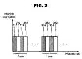
- FIG. 2is a timing sequence illustrating the process of conventional ALD process method.
- the vertical axisrepresents the process gas volume and the horizontal axis represents the processing time.
- the ALD process cycleis in the sequence of supply of first source gas 310 ⁇ purge 312 ⁇ supply of second source gas 314 ⁇ purge 312 .
- the source gas supplied to the reaction chamberis removed either by evacuating the reaction chamber using a vacuum pump or by feeding an inert purge gas into the reaction chamber.
- the invertors of the present inventionrecently disclosed in KR0273473 a plasma enhanced atomic layer deposition method(PEALD), that improves the reactivity, reduces the purging time and thus improves the deposition rate, and as a result, improves the productivity of the deposition apparatus.
- PEALDplasma enhanced atomic layer deposition method
- the difference between the plasma enhanced atomic layer deposition method and the aforementioned conventional ALDis a faster deposition rate even though source gases with low reactivity are used.
- the plasma enhanced atomic layer deposition method disclosed hereincreases the deposition reaction rate by generating radicals and ions with high reactivity by using a plasma, thereby these radicals and ions actively participate in the reaction process.
- the plasma enhanced ALD methodhas been disclosed in the patent application KR99-23078, “Chemical Deposition Reactor”, which invention reduces the volume of the reaction chamber, provides a means of even flow of the source gases when these gases supplied, and removed through the gas inlet tube and the gas outlet tube, respectively, flows over the substrate, and provided a means of generating a plasma.
- a plasmamay not be generated because of the fact that two electrodes used for applying RF power for plasma generation are electrically shorted due to the formation of a conductive thin film, and therefore, a conductive thin film may not be formed by using this apparatus along with the plasma enhanced atomic layer deposition method disclosed in the present invention.
- the object of the present inventionis to construct a reactor within which the process gases are replaced in a short period of time in order to process atomic layer deposition method, and also within which a plasma is generated over the surface area of a substrate, thereby even if a conductive thin layers are deposited, without causing the aforementioned electrical short in the reactor, and at the same time the atomic layer deposition process can easily be carried out, and is to provide an apparatus for forming a high quality thin film by using the plasma enhanced atomic layer deposition method according to the present invention.
- Another object of the present inventionis to provide a method of forming efficiently a good quality of thin film, even if the source gases do not react with each other easily or the reactivity is very weak, by using a plasma enhanced atomic layer deposition apparatus according to the present invention.
- the plasma enhanced atomic layer deposition apparatusis equipped with a substrate carrier that supports a substrate, a reactor within which said substrate carrier is mounted, within this reactor a showerhead that supplies source gases uniformly on the surface of a substrate, gas inlet and outlet tubes that feeds and removes gases into and out of a reactor, and a plasma generating unit that accelerates thin film deposition process in the reactor into which this plasma generating unit is mounted.
- a process gas supply and purge systemthat supplies and removes process gases through a gas inlet and gas outlet tubes in a combination of time-divisional manner, is installed in the PEALD tool, and finally a controller that control and manages the entire system is also installed.
- the process gas supply and removal system of the plasma enhanced atomic layer deposition apparatusmakes it possible to supply (process gas inlet) and remove (process gas outlet) into and out of a reactor in short time interval in such a way that the gas supply and removal process take place in a fashion of a combination of time-divisional sequence, and also the controller of said apparatus controls the reactor, the plasma generation unit inside of the reactor, the process gas supply and removal system including a gas evacuation vacuum pump and the deposition chamber system (reactor system).
- a process gas inlet tube and a process gas outlet tubeare installed symmetrically and concentrically with respect to substrate inside the reactor in order to supply and distribute the process gas uniformly over the substrate within the reaction space.
- the process gas inlet tube and the process gas outlet tubeare placed centrally with respect to the substrate and in the peripheral area, respectively, in the reactor.
- both gas inlet and gas outlet tubesare placed at the center of the upper part of the reactor and for this a set of concentrically structured two tubes is used.
- the process gas inlet tubemay be placed around the peripheral area of the substrate.
- a showerheadis mounted for an even distribution of the process gas, and according to the present invention this showerhead has a shape of the open end of a horn.
- This horn-shaped showerheadcan have many different shapes, for example, the edge of said horn may have an S-shape.
- the commonality in the horn-shaped showerheadis that the shape of the inner surface of the showerhead is streamlined-shape so that the process gas supplied though a gas inlet tube, the process gas is distributed evenly and uniformly along the inner surface of the showerhead.
- a grid with many holes or grids for dispersing a gasis mounted in parallel with the substrate. This grid disperses the process gas evenly and uniformly over the surface of the substrate.
- the showerheadis horn-shaped for the reason of reducing the volume that the process gas occupies. Another reason for using a horn-shaped showerhead is to eliminate any corners inside the showerhead, in order to prevent the process gas from being trapped by and around these undesirable corners, thereby the flow of the process gas is curled around these corners, and as a result, these corners interfere with the uniform flow of the process gas.
- the horn-shaped showerheadhelps the process gas flow uniformly, evenly and is smoothly.
- a volume adjusting horn and a gas dispersion perforated grid within the showerheadare the major parts forming a (+) electrode, the remaining metallic parts form a ( ⁇ ) electrode. Therefore, the plasma is generated only in the “reaction chamber” in the reaction space. In other words, the plasma is generated between the showerhead and the substrate carrier, and practically on the surface of the substrate.
- the showerhead insulating wallmade of non-conducting material of the shower head unit, and fixes the showerhead to the reactor.
- a barrier layer of plasma generationis provided between the insulating wall of the showerhead and the reactor wall. Formation of a conducting layer on the outer face of the insulating wall of the showerhead is prevented by blocking the flow of the process gas through the slits between the barrier layer of plasma generation and the insulating wall of the showerhead by continuously pushing an inert gas through said “slits” between said barrier layer of plasma generation and said insulating layer of said showerhead.
- Radio frequency connection terminalsare connected to the shower head for supplying RF (radio frequency) power to it.
- Said radio frequency connection terminalis made of a tube-shaped metallic material and when desired RF power is supplied through terminal, an inert gas can be supplied through the space between the showerhead insulating wall and the barrier wall of plasma generation.
- the process gas inlet tubeis connected to said showerhead through a micro-feeding tube assembly made of insulating materials.
- This micro-feeding tube assemblyhas more than one micro-tube in the middle of it, thereby said process gas is fed to the showerhead, but the plasma is blocked from reversed flow of reaction gas that may remain in the reactor or may be supplied to the reactor and also blocked from any leakage.
- the length of this micro-feed tube and the diameter of the micro-tuberare determined in such a way that the plasma does not leak.
- the substrate carrieris located in the lower part of the reactor and between the substrate carrier and the reactor wall there is a flat thin washer-like gas sealer ring for not only preventing the leakage or outflow of the process gas out of the reaction space, but also blocking the unnecessary film formation on the surface of the substrate carrier by blocking the contact of the process gas and the substrate carrier. Formation of unnecessary thin film does not occur even when the plasma is generated because the process gas does not contact with the substrate carrier.
- said gas sealer ringplays a key role of preventing the operational hindrance of the substrate carrier driver ever if the process gas is leaked into the external operational space of the substrate carrier, which space is filled with an inert gas such as Ar, thereby unnecessary metallic film is formed on the substrate carrier support and driver mechanisms.
- the substrate carrieris supported by a center support pin, center shaft, a plurality of driver shafts. Also, the substrate carrier moves up and down by a pneumatic cylinder linked to the driver shafts, thereby a substrate can be loaded onto and unloaded from the substrate carrier.
- a pneumatic cylinder linked to the driver shaftsthereby a substrate can be loaded onto and unloaded from the substrate carrier.
- the reactoris enclosed by the reactor body an inert gas is fed through the inert gas inlet tube and is removed through the inert gas outlet tube, where the inert gas inlet and outlet tubes are installed in the reactor body.
- the pneumatic cylindersare mounted outside of the reactor body.
- heatersare installed in the reactor walls and underneath the substrate carrier, thereby the substrate and the reactor body can be heated to a desired level, if necessary.
- the reactor bodyis electrically grounded, and through the driver shafts, the substrate carrier is also grounded. Also, the reactor walls are connected to the reactor body, and therefore, the reactor walls are electrically grounded.
- a method of forming thin films by using plasma activation even when a source gas containing metallic elements does not react in a reactor, process gas includes this source gas(or deposition gas) and a purge gas,is disclosed.
- a substrateis loaded on the substrate carrier in a reactor.
- said source gasis fed into the reactor, supply of said deposition gas(or source gas) is ceased, and while said purge gas is fed into the reactor, plasma is generated in order to activate the film deposition reaction.
- said methodcomprises the steps of feeding a source gas into a reactor, feeding a purge gas, generating plasma, and repeating said steps for a specified number of times in order to deposit a film to a desired thickness, thereby, forming a conducting layer of a thin film.
- micro-feeding tube assemblyin which a plurality of fine and small micro-tubes are arranged in parallel, and said process gases are fed through said gas inlet tube and then through said micro-feeding tube assembly and finally into the showerhead assembly area inside the reactor.
- FIGS. 1 a and 1 bare conceptual schematic drawings of conventional chemical vapor deposition apparatus.
- FIG. 2is a timing diagram for a thin film formation process using a conventional chemical vapor deposition apparatus showing a sequence of the process gas supply and removal.
- FIG. 3is a schematic drawing of the cross-section of plasma enhanced atomic layer deposition apparatus according to the present invention
- FIG. 4is a timing diagram for a thin film formation process using an plasma enhanced vapor deposition apparatus according to the present invention showing a sequence of the process gas supply and removal as well as the plasma generation.
- FIG. 3is a cross-sectional schematic diagram of a plasma enhanced atomic layer deposition apparatus according to the Best Mode of the present invention.
- a heateris installed at the bottom part of the substrate carrier 560 so that it can control the temperature of the substrate 556 or the reaction space 554 as necessary.
- a heater 604 installed on the reactor walls 522may be if necessary used for increasing the temperature of the reactor which is the inside of the reactor wall.
- a substrate carrier 560At the upper part of the reactor wall 522 made of an alloy, a dual orifice tube assembly 516 and at the lower part of the reactor wall 522 , there is a substrate carrier 560 .
- the substrate carrier 560 and the reactor wall 522define the inner part of the reactor.
- a gas sealer ring 558is located between the top surface of the outer ring of the substrate carrier 560 and the bottom end of the reactor wall 522 , and this gas sealer ring 558 shaped as a thin flat washer-like with an inner side hovelled and outer side-square edged ring seals between the substrate carrier 560 and the reactor wall 522 as well as covers the top surface of the outer ring area of the substrate carrier 560 .
- the showerhead assembly( 540 , 542 ) comprises a volume adjusting horn 540 and a gas dispersion perforated grid 542 .
- the shape of the volume adjusting horn 540allows the process gas to distribute uniformly, evenly and smoothly over the substrate 556 , and at the same time, minimizes the volume of the inner part of the showerhead 552 .
- a gas dispersion perforated grid 542is mounted at the bottom part of the volume adjusting horn 540 .
- the showerhead assembly ( 540 , 542 ) and the bottom end of the gas inlet tube 510are connected through a micro-feeding tube assembly 536 , and therefore, the process gas enters into the gas inlet tube 510 and flows in the direction of arrows indicated, and continue to flow through the micro-feeding tube assembly 536 and then to the inner part 552 of the showerhead assembly.
- the shape of the volume adjusting horn 540is designed to minimize its volume for proper processing of a substrate, and yet to let a process gas to flow smoothly and evenly over a substrate 556 as well as to make the removal of a process gas and filling a incoming process gas easily and fast. More specifically, during a sequential supply of process gases, the possibility of the vapor state reaction between a new process gas and the residual gas of the previous supply cycle accumulated and remained unnecessarily in the inner part of the showerhead 552 .
- the dual orifice tube assembly 516is, as described previously, connected to the inlet opening of the reactor wall 522 and the outer tube of the dual orifice tube assembly 516 is connected to a vacuum pump 598 through a gas outlet tube 518 .
- the process gas entered into the reaction space 554 by being dispersed evenly through the gas dispersion perforated grid(or showerhead grid) 542travels through the gap 526 (passage of removal gas indicated by arrows) between the reactor wall 522 and the plasma generation barrier 528 , and then through the gas outlet tube 518 , and then finally to the vacuum pump 598 .
- the arrowsindicate the direction of the flow of a process gas.
- the reactor wall 522may be heated by using a heater 604 as necessary.
- the radio frequency connection terminal 566is made of a metallic tube for receiving a radio frequency power from outside and an insulation tube 568 made of an insulating material, and this terminal 566 is connected electrically to both volume adjusting horn 540 and the gas dispersion perforated grid 542 as a plus (+) polarity.
- the radio frequency connection terminal 566shielded with an insulating tube 568 is connected to the volume adjusting horn 540 through the reactor body 600 , the reactor wall 522 , the plasma generation barrier 528 and the showerhead insulation wall 538 .
- the radio frequency connection terminal 566is electrically insulated form the reactor body 600 , reactor wall 522 and the plasma generation barrier wall 528 , whereas the radio frequency connection terminal 566 which is a conductor, is electrically connected only to the volume adjusting horn 540 .
- the showerhead insulating wall 538is electrically insulated from the radio frequency terminal 566 because the showerhead insulating wall 538 is made of an insulating material.
- the gas inlet tube 510(on an inner tube) is a conductor, and because the micro-feeding tube assembly 536 is made of an insulating material, the showerhead assembly 540 , 542 is electrically insulated from the reactor wall 522 as well as the reactor body 600 . And the substrate 556 as well as the substrate carrier 560 is electrically connected to ground 594 through the driver shaft 580 and the reactor body 600 . Therefore, when radio frequency power is applied by using an RF generator (not shown), plasma is generated between the showerhead assembly 540 , 542 as a positive (+) polarity and the substrate 556 as well as the substrate carrier 560 as a negative ( ⁇ ) polarity.
- the plasma generation barrier wall 528is installed between the showerhead insulation wall 538 and the reactor wall 522 in order to prevent any electrical short between the showerhead assembly 540 , 542 and any metallic part within the reactor such as the reactor wall 522 due to a formation of a conductive thin film on the surface of the showerhead insulation wall 538 which is used for mounting the showerhead assembly 540 , 542 to the reactor body 600 .
- the plasma generation barrier wall 528is electrically connected to ground 594 through the gas inlet tube 510 and the reactor body 600 . Therefore, plasma is not generated in the passage of removal gas 526 between the plasma generation barrier wall 528 and the reactor wall 522 , thereby a conductive thin film is not formed, and therefore, this passage 526 is used as a passage for process gases.
- the passage of inert gas 544 between the showerhead insulation wall 538 and the plasma generation barrier wall 528allows plasma to generate even if in the lower tip end part of the showerhead insulation wall 538 near the substrate carrier 560 has a conductive thin film is formed, and also by supplying an inert gas continuously through the narrow passage of inert gas 544 , plasma generation near the end part of the passage of inert gas 544 , and formation of a conductive thin film is blocked, and thereby, this prevents an electrical short between the showerhead assembly 540 , 542 and ground 594 from occurring.
- micro-feeding tube assembly 536with a plural of small and fine tubes with small in diameter, a plasma generation inside the micro-feeding tube assembly 536 , thereby formation of a thin conductive film inside of the micro-feeding tube assembly 536 is prevented.
- the inventioncomprises four(4) significant inventive parts.
- First oneis the shape of the volume adjusting horn 540 of the showerhead assembly 540 , 542
- the secondis the structure of the micro-feeding tube assembly 536
- the thirdis the arrangement of a thin gap provided between the showerhead insulation wall 538 so that an inert gas such as Argon(Ar) is continuously supplied
- the fourthis an efficient way of structuring a plasma generation unit by arranging and using a radio frequency power connection terminal 566 made of a conducting tube and an insulating tube 568 made of an electrically insulating material.
- said micro-feeding tube assembly 536structured with a plural of tubes with small in diameter, in parallel, is assembled to connect the showerhead assembly 540 , 542 and the gas inlet tube so that the micro-feeding tube assembly 536 suppresses the plasma generation while the inert gas flows steadily.
- Aforementioned micro-feeding tube assembly 536is made of insulating materials. The size of the diameter of the small tubes in the micro-feeding tube assembly 536 is chosen in such a way that the size is small enough so that plasma generation does not occur, yet an adequate amount of gas flows through steadily.
- the over-all diameter of the micro-feeding tube assemblyis about 6 mm and its length is about 20 mm and the diameter of the small tubes is about 0.6 mm and eight(8) of them altogether are used to construct a micro-feeding tube assembly 536 .
- a set of long tubessufficiently longer than the distance between the gas dispersion perforated grid 542 and the substrate 556 so that the occurrence of plasma generation inside these tubes may be prevented.
- the upper part of the thickness of the showerhead insulation wall 538must be made thicker in order to accommodate the extra length of the gas dispersing perforated grid 542 as well as other parts of the reactor assembly must be significantly enlarged, thereby the cost and material for constructing such a part increases.
- the frequency of collisions between the electrons and gas atoms or molecules while the electrons moving towards electrodesoften being accelerated due to the electric and magnetic fields.
- a potential difference between the reactor wall 522 and the showerhead insulation wall 538may exist and therefore a plasma state may be generated here, and as a result, on the inside surface of the reactor wall 522 and the outside surface of the showerhead insulation wall 538 , a conducting thin film may be formed due to the reaction of the process gas occurring while such process gas is passing through the reactor space 554 , the reactor wall 552 , and then the showerhead insulation wall 538 .
- the conducting thin film formed on the outer surface of the showerhead insulation wall 538may cause an electrical short between the showerhead assembly 540 , 542 and the reactor wall 522 , which is connected to ground.
- a plasma generation barrier wall 528is constructed between the reactor wall 522 and the showerhead insulation wall 538 , and also connect electrically with the reactor wall 522 through the gas inlet tube 510 (inner tube), the plasma generation does not take place due to the fact that there is no potential difference between the plasma generation barrier wall 528 and the reactor wall 522 . If the distance(space) between the plasma generation barrier wall 528 and the showerhead insulation wall 538 is reduced, the plasma generation in this neighborhood can be suppressed.
- the plasma generationtakes place mainly in the relatively spacious reaction space 554 between the gas dispersion perforated grid 542 and the substrate 556 where the showerhead assembly 540 , 542 to which radio frequency power is applied with respect to grounded.
- an inert gassuch as Argon(Ar) continuously during the film formation period through the gaps 544 , 548 , 526 between the plasma generation barrier wall 528 and the showerhead insulation wall 538 in the direction of arrows, undesired flow of process gases through the end part of the passage of inert gas 548 as well as the passage of inert gas 544 can be prevented.
- the necessary inert gas for above stepis supplied through a tube-shaped radio frequency power connection terminal 566 .
- the inert gasis supplied through the hole at the center of the radio frequency power connection terminal 566 and then through the hole 564 in the tube, and then through the gaps between the showerhead insulation wall 538 and the plasma generation barrier wall 528 as indicated by arrows.
- the inert gasthen travels the gaps and passage ways 620 , 624 , 626 , 628 and to the passage of inert gas 544 and then continue to flow following the arrows.
- such passage ways and buffering spacesare preferably arranged so that a proper, adequate, and smooth flow of the inert gas is achieved.
- Such arrangementpreferably provides a uniform and even flow of the inert gas through out the inert gas passage ways as indicated by arrows even if the location of the radio frequency connection terminal 566 is located off centered, as shown in the FIG. 3 .
- the gap size of the passage of inert gas 544is 0.4 mm and the gap size of the end part of the passage of inert gas 548 is 0.4 mm, respectively, and the outside diameter of the showerhead insulation wall 538 is 210 mm for the 200 mm wafer
- a gasis supplied at the flow rate of 20 sccm
- the flow velocity of the gas at the gaps of the passage of inert gas 544 and the end part of the passage of inert gas 548is 19 mm/s at the temperature of 25° C. and the pressure of 5 Torr. As the temperature increases, the flow velocity increases.
- the inert gasis forcibly supplied through the inert gas inlet tube 566 and flows, as indicated by arrows, through the first reservoir ring 620 , the inert gas passage way 622 , the second reservoir ring 624 , the third reservoir ring 626 and the fourth reservoir ring 628 , and then through the passage of inert gas which is the gap between the showerhead insulation wall 538 and the plasma generation barrier wall 528 , and then continue to flow following the arrows, and eventually flows through the end part of the passage of inert gas 548 which is the bottom part of the showerhead insulation wall 538 and the plasma generation barrier wall 528 , respectively, and finally joins with the process gas and this mixed gas
- the flow of the inert gas through the end part of the passage of inert gas 548blocks backflow of the process gas inside of the reaction space 554 flowing through the gap of the passage of inert gas 544 which is the gap between the showerhead insulation wall 538 and the plasma generation barrier wall 528 and flowing backwards against the flow of inert gas into the passage of inert gas 544 , and therefore, when a process gas containing metallic material is used, no undesirable conducting thin film is formed inside of the passage of inert gas 544 , particularly around the end part of the passage of inert gas 548 , and as a result, it does not create a problem of an electrical short. This prolongs the life of the usage of the surrounding areas of the reaction space 554 .
- a conducting thin filmis formed only in the areas where a process gas is supplied and present and the plasma generation occurs. This means that no conductive thin film is formed between the plasma generation barrier wall 528 and the reactor wall 522 because no plasma is generated, and that no conductive thin film is formed between the plasma generation barrier wall 528 and the showerhead insulation wall 538 because no process gas is supplied and present. Consequently, a conducting thin film is formed only within the reaction space 554 , where a substrate 556 is located and no conducting thin film is formed outside the reaction space 544 , and therefore, an electrical short is blocked even if the process of formation of a conducting thin film is repeated.
- a reactor body 600includes the reactor wall 522 along with the elements installed inside including a substrate carries 560 , an inert gas inlet tube 590 and an inert gas outlet tube 592 equipped with an on-off valves for gases, respectively, where the exact location of these gas inlet and outlet tubes is not significant.
- the radio frequency connection terminal 566is connected to the showerhead assembly 540 , 542 though the reactor body 600 as well as the reactor wall 522 , and this installation process provides electrical insulation of the radio frequency connection terminal from the reactor body 600 as well as the reactor wall 522 .
- a radio frequency connection terminal 566is connected to a showerhead assembly 540 , 542 through a reactor body 600 , a reactor wall 522 , a plasma generation barrier wall 528 and then a showerhead insulation wall 538 , and the connections are made with the reactor body 600 , the reactor wall 522 and the plasma generation barrier wall 528 in such a way that the radio frequency connection terminal is electrically insulated from the parts described above.
- the reactor body 600has mainly two parts of a top cover and the bottom body.
- leakage of inside of the reaction space 554can be prevented by maintaining the pressure of the inert gas that is supplied through the inert gas inlet tube 590 and then out through the inert gas outlet tube 592 higher than the pressure of the gas inside of the reaction space 554 .
- the substrate carrier driven assembly for driving a substrate carrier 560consists of primarily pneumatic cylinders 584 , a drive shaft 580 that connects the pneumatic cylinder 584 and a substrate carrier 560 , and a girding plate 578 that maintains a balance among the drive shafts 580 .
- the substrate carrier connected to an pneumatic cylinder 584moves downwards, so that the reactor wall 522 and the substrate carrier 560 are separated and the reaction space 554 is opened.
- the center support pin 572is connected to the center axis stopper pin 574 , and this stopper pin 574 stops the downward movement at a given height.
- the substrate carrieris separated from the substrate 556 since it is supported by the center support pin 572 and stops by the center support stopper pin 574 , but the substrate carrier 560 continues to move downwards as the pneumatic cylinders 584 pulls the substrate carrier 560 further down.
- the substrate 556stops at a given height so that a robot arm (not shown) is able to load or unload the substrate 556 .
- the lengths of the center support stopper pin 574 and the center support pin 572are adjusted as necessary in order to accommodate the movements of a robot arm(not shown).
- the volume adjusting horn 540that has a shape of a horn makes the flow of the process gas smooth and evenly distributed, while the volume of the inside of the showerhead is minimized and thus the exchange of the process gases are done easily and quickly, thereby potentially the unnecessary reaction between the residual gas remained inside of the showerhead assembly 540 , 542 from previous process cycle and the subsequently supplied gas is minimized.
- the plasma generation between the showerhead assembly 540 , 542 and the process gas inlet tube 510can be suppressed, and also, by supplying an inert gas through the passage of inert gas between the grounded plasma generation barrier wall 528 and the showerhead insulation wall 538 , a thin film is formed only in the reaction space 554 between the gas dispersion perforated grid 542 and a substrate 556 , but no thin film is formed on other parts where a process gas flows, thereby a conducting thin film can be formed by using the plasma enhanced atomic layer deposition method without a problem of having electrical shorts. Furthermore, the process gas flows within the inside of the reactor, and does not contact with the reactor body 600 .
- FIG. 4is a timing diagram related to the best mode described above by using a plasma enhanced atomic layer deposition for illustration.
- the source gas 440 and the purge gas 442are supplied in a cycle of Tcycle in a sequence of 440 ⁇ 442 .
- plasma generation 446occurs for a specified duration of time by applying a radio frequency power 446 .
- a source gas 440includes a metallic element such as Titanium Tetra Chloride(TiCl 4 ) that is used for forming a metallic thin film, and the purge gas 442 is a gas that does not react with a deposition gas by simply mixing them, but, they reacts when activated by a plasma 446 .
- FIG. 5is a flowchart of typical process steps using a plasma enhanced atomic layer deposition apparatus according to the present invention.
- a substrate 556is loaded onto a substrate carrier 560 .(step 850 ).
- the temperature of the substrate 556is raised to a desired deposition temperature.(step 852 ).
- a source gas 440is supplied to a reaction space 554 .
- a purge gas 442is supplied to the reaction space 554 and remove the remaining deposition gas 440 .
- step 860through the radio frequency power connection terminal 566 , RF power is supplied and plasma 446 is generated in the reaction space 554 and the purge gas 442 mixed with source gas is activated.
- the plasma 446activates the deposition gas(source) 440 adsorbed on the surface of the substrate 556 and a thin film is formed.
- the RF poweris switched off. Once The RF power is disconnected, the density of the radicals and ions in the activated purge gas is decreased drastically, thereby the time required to feed the purge gas after the RF power is switched off can he reduced significantly.
- step 866is repeated by the specified number of times until the thin film is formed to a desired thickness.(step 866 and repeat of steps 854 through 866 as necessary).
- a thin filmcan be formed using only two types of gases by means of atomic layer deposition method, and this process makes the process gas supply and distribution system simple as well as the deposition process cycle time(Tcycle) can be reduced. Furthermore, according to the method of the present invention, even if source gas 440 and the purge gas 442 may be mixed in the areas of reaction space 554 , the gas inlet tube 510 , the gas outlet tube 518 and also near the gas exhaust area, the reaction does not take place, thereby undesirable particles are not generated.
- a thin film using Titanium Nitride(TiN)is formed by the conducting thin film formation method in accordance with the present invention of the plasma enhanced atomic layer deposition method.
- a source gas160 sccm of Argon(Ar) gas and Titanium Tetra-Chloride(TiCl 4 ) carried by Argon(Ar) gas of 100 sccm which passes through a source container were supplied through the shower head 540 in a reactor loaded with a substrate.
- a conductive thin film of Titaniumwas formed.
- 230 sccm of Argon gas and TiCl 4 (Titanium Tetra-Chloride) carried by Argon gas of 100 sccm which passes through a source containerwas supplied to the shower head assembly 540 , 542 .
- 100 sccm of Hydrogen(H 2 ) gas and 230 sccm of Argon gaswere supplied.
- 20 sccm of Argon gaswas supplied.
- the substrate temperaturewas set at 380° C.
- the RF powerwas set at 200 W and the pressure was set at 3 Torr.
- the duration of the source gas supplywas 0.2 second, the purge gas was supplied for 5.8 seconds.
- the purge gas supply time of 5.8 secondsfor the first 2.0 seconds, the RF power was switched off and only the purge gas was supplied.
- the purge gaswas supplied and also the RF power was turned on to generate plasma.
- the horn-shaped volume adjusting hornallows a uniform distribution and even flow of the gases, and at the same time, this shape minimizes the volume of the inside of the showerhead, thereby it makes the exchange of gases in the reactor easy and fast, and thus the reaction between the incoming gas into the reactor and the residual gas remaining from the previous process cycle is minimized due to the fact that a smooth horn-shaped showerhead minimizes the amount of unnecessary residual gas staying is the reactor after the pervious gas supply cycle.
- the micro-feeding tube assemblymade of a plural of small tubes in parallel, potentially, suppresses the plasma generation due to the potential difference between the showerhead assembly and the gas inlet tube.
- the forced flow of an inert gas through the gap between the plasma generation barrier wall and the showerhead insulation wallmakes the formation of thin film occur only inside of the reaction space which is the space between the gas dispersion perforated grid and the substrate, and since thin film is not formed on other parts even though a process gas flows, no electrical short takes place and a conducting thin film can be formed by using the plasma enhanced atomic layer deposition method according to the present invention. Therefore, since plasma is generated only in the reaction space between the gas dispersion perforated grid and the substrate, and on the other parts where the process gas flows, the deposition of thin film is suppressed, the plasma enhanced atomic layer deposition method according to the present invention can be used for forming conducting thin films.
- any biased flow of the process gases towards the location of gas outlet tube inside the reaction spacecan be avoided, and the flow of process gases flows symmetrically and balanced way in the reaction space, thereby uniform deposition of thin film is possible.
- the showerhead assembly and the reaction spacecan be constructed within a smaller volume. Therefore, for the process of sequentially supplying various types of process gases, the exchange of gases becomes easy and fast.
- the plasma enhanced atomic layer deposition methodallows an efficient ways of forming thin film even when the process gases have vary weak reaction property. Furthermore, by using the ALD method disclosed here, within the process cycle, the purge gas supply time can be minimized, and thereby the over-all process time can be shortened. Further, according to the present invention, generation of undesirable particles at the exhaust end of the reactor assembly can be reduced.
Landscapes
- Chemical & Material Sciences (AREA)
- Engineering & Computer Science (AREA)
- Chemical Kinetics & Catalysis (AREA)
- General Chemical & Material Sciences (AREA)
- Physics & Mathematics (AREA)
- Organic Chemistry (AREA)
- Metallurgy (AREA)
- Mechanical Engineering (AREA)
- Materials Engineering (AREA)
- Plasma & Fusion (AREA)
- Manufacturing & Machinery (AREA)
- Analytical Chemistry (AREA)
- Condensed Matter Physics & Semiconductors (AREA)
- General Physics & Mathematics (AREA)
- Power Engineering (AREA)
- Microelectronics & Electronic Packaging (AREA)
- Computer Hardware Design (AREA)
- Electromagnetism (AREA)
- Chemical Vapour Deposition (AREA)
Abstract
Description
Claims (46)
Priority Applications (1)
| Application Number | Priority Date | Filing Date | Title |
|---|---|---|---|
| US11/449,039US20060276037A1 (en) | 2001-08-06 | 2006-06-06 | Plasma enhanced atomic layer deposition (PEALD) equipment and method of forming a conducting thin film using the same thereof |
Applications Claiming Priority (1)
| Application Number | Priority Date | Filing Date | Title |
|---|---|---|---|
| PCT/KR2001/001333WO2003023835A1 (en) | 2001-08-06 | 2001-08-06 | Plasma enhanced atomic layer deposition (peald) equipment and method of forming a conducting thin film using the same thereof |
Related Child Applications (1)
| Application Number | Title | Priority Date | Filing Date |
|---|---|---|---|
| US11/449,039ContinuationUS20060276037A1 (en) | 2001-08-06 | 2006-06-06 | Plasma enhanced atomic layer deposition (PEALD) equipment and method of forming a conducting thin film using the same thereof |
Publications (2)
| Publication Number | Publication Date |
|---|---|
| US20040231799A1 US20040231799A1 (en) | 2004-11-25 |
| US7138336B2true US7138336B2 (en) | 2006-11-21 |
Family
ID=19198433
Family Applications (2)
| Application Number | Title | Priority Date | Filing Date |
|---|---|---|---|
| US10/486,311Expired - LifetimeUS7138336B2 (en) | 2001-08-06 | 2001-08-06 | Plasma enhanced atomic layer deposition (PEALD) equipment and method of forming a conducting thin film using the same thereof |
| US11/449,039AbandonedUS20060276037A1 (en) | 2001-08-06 | 2006-06-06 | Plasma enhanced atomic layer deposition (PEALD) equipment and method of forming a conducting thin film using the same thereof |
Family Applications After (1)
| Application Number | Title | Priority Date | Filing Date |
|---|---|---|---|
| US11/449,039AbandonedUS20060276037A1 (en) | 2001-08-06 | 2006-06-06 | Plasma enhanced atomic layer deposition (PEALD) equipment and method of forming a conducting thin film using the same thereof |
Country Status (4)
| Country | Link |
|---|---|
| US (2) | US7138336B2 (en) |
| EP (1) | EP1421606A4 (en) |
| JP (1) | JP4666912B2 (en) |
| WO (1) | WO2003023835A1 (en) |
Cited By (77)
| Publication number | Priority date | Publication date | Assignee | Title |
|---|---|---|---|---|
| US20050034664A1 (en)* | 2001-11-08 | 2005-02-17 | Koh Won Yong | Apparatus for depositing |
| US20050285982A1 (en)* | 2004-06-29 | 2005-12-29 | Lg.Philips Lcd Co., Ltd. | Apparatus for manufacturing liquid crystal display device and liquid crystal display device manufactured using the same |
| US20060276037A1 (en)* | 2001-08-06 | 2006-12-07 | Lee Chun S | Plasma enhanced atomic layer deposition (PEALD) equipment and method of forming a conducting thin film using the same thereof |
| US20070040634A1 (en)* | 2005-03-30 | 2007-02-22 | Matsushita Electric Industrial Co., Ltd. | Transmission line |
| US20070051312A1 (en)* | 2003-08-07 | 2007-03-08 | Ofer Sneh | Perimeter partition-valve with protected seals and associated small size process chambers and multiple chamber systems |
| US20070215036A1 (en)* | 2006-03-15 | 2007-09-20 | Hyung-Sang Park | Method and apparatus of time and space co-divided atomic layer deposition |
| US20070218702A1 (en)* | 2006-03-15 | 2007-09-20 | Asm Japan K.K. | Semiconductor-processing apparatus with rotating susceptor |
| US20080075858A1 (en)* | 2006-09-22 | 2008-03-27 | Asm Genitech Korea Ltd. | Ald apparatus and method for depositing multiple layers using the same |
| US20080113110A1 (en)* | 2006-10-25 | 2008-05-15 | Asm America, Inc. | Plasma-enhanced deposition of metal carbide films |
| US7388246B2 (en) | 2002-08-29 | 2008-06-17 | Micron Technology, Inc. | Lanthanide doped TiOx dielectric films |
| US20080157171A1 (en)* | 2006-12-29 | 2008-07-03 | Prashant Majhi | Dielectric barrier for nanocrystals |
| US7405454B2 (en) | 2003-03-04 | 2008-07-29 | Micron Technology, Inc. | Electronic apparatus with deposited dielectric layers |
| US7410910B2 (en) | 2005-08-31 | 2008-08-12 | Micron Technology, Inc. | Lanthanum aluminum oxynitride dielectric films |
| US20080241384A1 (en)* | 2007-04-02 | 2008-10-02 | Asm Genitech Korea Ltd. | Lateral flow deposition apparatus and method of depositing film by using the apparatus |
| US20080274617A1 (en)* | 2007-05-02 | 2008-11-06 | Asm America, Inc. | Periodic plasma annealing in an ald-type process |
| US20090104375A1 (en)* | 2007-09-17 | 2009-04-23 | L'air Liquide-Societe Anonyme Pour L'etude Et Exploitation Des Procedes Georges Claude | Neutral ligand containing precursors and methods for deposition of a metal containing film |
| US20090137103A1 (en)* | 2007-11-27 | 2009-05-28 | Semiconductor Energy Laboratory Co., Ltd. | Method for manufacturing semiconductor device |
| US20090136665A1 (en)* | 2007-11-27 | 2009-05-28 | Asm Genitech Korea Ltd. | Atomic layer deposition apparatus |
| US20090156015A1 (en)* | 2007-12-18 | 2009-06-18 | Asm Genitech Korea Ltd. | Deposition apparatus |
| US7560793B2 (en) | 2002-05-02 | 2009-07-14 | Micron Technology, Inc. | Atomic layer deposition and conversion |
| WO2009089244A1 (en)* | 2008-01-10 | 2009-07-16 | Applied Materials, Inc. | Showerhead insulator and etch chamber liner |
| US7572695B2 (en) | 2005-05-27 | 2009-08-11 | Micron Technology, Inc. | Hafnium titanium oxide films |
| US7575978B2 (en)* | 2005-08-04 | 2009-08-18 | Micron Technology, Inc. | Method for making conductive nanoparticle charge storage element |
| US20090211707A1 (en)* | 2008-02-22 | 2009-08-27 | Hermes Systems Inc. | Apparatus for gas distribution and its applications |
| US7588988B2 (en) | 2004-08-31 | 2009-09-15 | Micron Technology, Inc. | Method of forming apparatus having oxide films formed using atomic layer deposition |
| US7611751B2 (en) | 2006-11-01 | 2009-11-03 | Asm America, Inc. | Vapor deposition of metal carbide films |
| US7662729B2 (en) | 2005-04-28 | 2010-02-16 | Micron Technology, Inc. | Atomic layer deposition of a ruthenium layer to a lanthanide oxide dielectric layer |
| US7666474B2 (en) | 2008-05-07 | 2010-02-23 | Asm America, Inc. | Plasma-enhanced pulsed deposition of metal carbide films |
| US7670646B2 (en) | 2002-05-02 | 2010-03-02 | Micron Technology, Inc. | Methods for atomic-layer deposition |
| US7687409B2 (en) | 2005-03-29 | 2010-03-30 | Micron Technology, Inc. | Atomic layer deposited titanium silicon oxide films |
| US20100279008A1 (en)* | 2007-09-12 | 2010-11-04 | Tokyo Electron Limited | Film deposition apparatus and film deposition method |
| US7927948B2 (en) | 2005-07-20 | 2011-04-19 | Micron Technology, Inc. | Devices with nanocrystals and methods of formation |
| US20110168094A1 (en)* | 2010-01-13 | 2011-07-14 | Honda Motor Co., Ltd. | Plasma film forming apparatus |
| US20110197815A1 (en)* | 2007-11-27 | 2011-08-18 | Semiconductor Energy Laboratory Co., Ltd. | Method of manufacturing semiconductor device, film deposition method, and film deposition apparatus |
| US20120024479A1 (en)* | 2010-07-30 | 2012-02-02 | Applied Materials, Inc. | Apparatus for controlling the flow of a gas in a process chamber |
| US8216376B1 (en)* | 2009-01-15 | 2012-07-10 | Intermolecular, Inc. | Method and apparatus for variable conductance |
| US8273178B2 (en) | 2008-02-28 | 2012-09-25 | Asm Genitech Korea Ltd. | Thin film deposition apparatus and method of maintaining the same |
| US20120266821A1 (en)* | 2005-01-18 | 2012-10-25 | Asm America, Inc. | Reaction system for growing a thin film |
| US8367506B2 (en) | 2007-06-04 | 2013-02-05 | Micron Technology, Inc. | High-k dielectrics with gold nano-particles |
| US8841182B1 (en) | 2013-03-14 | 2014-09-23 | Asm Ip Holding B.V. | Silane and borane treatments for titanium carbide films |
| US8846550B1 (en) | 2013-03-14 | 2014-09-30 | Asm Ip Holding B.V. | Silane or borane treatment of metal thin films |
| US8993055B2 (en) | 2005-10-27 | 2015-03-31 | Asm International N.V. | Enhanced thin film deposition |
| US9394609B2 (en) | 2014-02-13 | 2016-07-19 | Asm Ip Holding B.V. | Atomic layer deposition of aluminum fluoride thin films |
| US9631272B2 (en) | 2008-04-16 | 2017-04-25 | Asm America, Inc. | Atomic layer deposition of metal carbide films using aluminum hydrocarbon compounds |
| US9704716B2 (en) | 2013-03-13 | 2017-07-11 | Asm Ip Holding B.V. | Deposition of smooth metal nitride films |
| US9786491B2 (en) | 2015-11-12 | 2017-10-10 | Asm Ip Holding B.V. | Formation of SiOCN thin films |
| US9786492B2 (en) | 2015-11-12 | 2017-10-10 | Asm Ip Holding B.V. | Formation of SiOCN thin films |
| US9941425B2 (en) | 2015-10-16 | 2018-04-10 | Asm Ip Holdings B.V. | Photoactive devices and materials |
| US9972501B1 (en) | 2017-03-14 | 2018-05-15 | Nano-Master, Inc. | Techniques and systems for continuous-flow plasma enhanced atomic layer deposition (PEALD) |
| US10002936B2 (en) | 2014-10-23 | 2018-06-19 | Asm Ip Holding B.V. | Titanium aluminum and tantalum aluminum thin films |
| US10186420B2 (en) | 2016-11-29 | 2019-01-22 | Asm Ip Holding B.V. | Formation of silicon-containing thin films |
| US10458019B2 (en) | 2012-11-02 | 2019-10-29 | Industrial Technology Research Institute | Film deposition apparatus having a peripheral spiral gas curtain |
| US10504901B2 (en) | 2017-04-26 | 2019-12-10 | Asm Ip Holding B.V. | Substrate processing method and device manufactured using the same |
| US10600637B2 (en) | 2016-05-06 | 2020-03-24 | Asm Ip Holding B.V. | Formation of SiOC thin films |
| US10643925B2 (en) | 2014-04-17 | 2020-05-05 | Asm Ip Holding B.V. | Fluorine-containing conductive films |
| US10847529B2 (en) | 2017-04-13 | 2020-11-24 | Asm Ip Holding B.V. | Substrate processing method and device manufactured by the same |
| US10872804B2 (en) | 2017-11-03 | 2020-12-22 | Asm Ip Holding B.V. | Apparatus and methods for isolating a reaction chamber from a loading chamber resulting in reduced contamination |
| US10872803B2 (en) | 2017-11-03 | 2020-12-22 | Asm Ip Holding B.V. | Apparatus and methods for isolating a reaction chamber from a loading chamber resulting in reduced contamination |
| US10991573B2 (en) | 2017-12-04 | 2021-04-27 | Asm Ip Holding B.V. | Uniform deposition of SiOC on dielectric and metal surfaces |
| US10998209B2 (en) | 2019-05-31 | 2021-05-04 | Applied Materials, Inc. | Substrate processing platforms including multiple processing chambers |
| US11087959B2 (en) | 2020-01-09 | 2021-08-10 | Nano-Master, Inc. | Techniques for a hybrid design for efficient and economical plasma enhanced atomic layer deposition (PEALD) and plasma enhanced chemical vapor deposition (PECVD) |
| US11158500B2 (en) | 2017-05-05 | 2021-10-26 | Asm Ip Holding B.V. | Plasma enhanced deposition processes for controlled formation of oxygen containing thin films |
| US11396702B2 (en)* | 2016-11-15 | 2022-07-26 | Asm Ip Holding B.V. | Gas supply unit and substrate processing apparatus including the gas supply unit |
| US11600507B2 (en) | 2020-09-09 | 2023-03-07 | Applied Materials, Inc. | Pedestal assembly for a substrate processing chamber |
| US11610799B2 (en) | 2020-09-18 | 2023-03-21 | Applied Materials, Inc. | Electrostatic chuck having a heating and chucking capabilities |
| US11640900B2 (en) | 2020-02-12 | 2023-05-02 | Nano-Master, Inc. | Electron cyclotron rotation (ECR)-enhanced hollow cathode plasma source (HCPS) |
| US11674227B2 (en) | 2021-02-03 | 2023-06-13 | Applied Materials, Inc. | Symmetric pump down mini-volume with laminar flow cavity gas injection for high and low pressure |
| US11749542B2 (en) | 2020-07-27 | 2023-09-05 | Applied Materials, Inc. | Apparatus, system, and method for non-contact temperature monitoring of substrate supports |
| US11817331B2 (en) | 2020-07-27 | 2023-11-14 | Applied Materials, Inc. | Substrate holder replacement with protective disk during pasting process |
| US12002668B2 (en) | 2021-06-25 | 2024-06-04 | Applied Materials, Inc. | Thermal management hardware for uniform temperature control for enhanced bake-out for cluster tool |
| US12080571B2 (en) | 2020-07-08 | 2024-09-03 | Applied Materials, Inc. | Substrate processing module and method of moving a workpiece |
| US12142479B2 (en) | 2020-01-17 | 2024-11-12 | Asm Ip Holding B.V. | Formation of SiOCN thin films |
| US12180586B2 (en) | 2021-08-13 | 2024-12-31 | NanoMaster, Inc. | Apparatus and methods for roll-to-roll (R2R) plasma enhanced/activated atomic layer deposition (PEALD/PAALD) |
| US12195314B2 (en) | 2021-02-02 | 2025-01-14 | Applied Materials, Inc. | Cathode exchange mechanism to improve preventative maintenance time for cluster system |
| US12197125B2 (en) | 2020-12-22 | 2025-01-14 | Nano-Master, Inc. | Mask and reticle protection with atomic layer deposition (ALD) |
| US12341005B2 (en) | 2020-01-17 | 2025-06-24 | Asm Ip Holding B.V. | Formation of SiCN thin films |
| US12359315B2 (en) | 2019-02-14 | 2025-07-15 | Asm Ip Holding B.V. | Deposition of oxides and nitrides |
Families Citing this family (387)
| Publication number | Priority date | Publication date | Assignee | Title |
|---|---|---|---|---|
| US6878206B2 (en) | 2001-07-16 | 2005-04-12 | Applied Materials, Inc. | Lid assembly for a processing system to facilitate sequential deposition techniques |
| JP2005504885A (en) | 2001-07-25 | 2005-02-17 | アプライド マテリアルズ インコーポレイテッド | Barrier formation using a novel sputter deposition method |
| US9051641B2 (en) | 2001-07-25 | 2015-06-09 | Applied Materials, Inc. | Cobalt deposition on barrier surfaces |
| US20030029715A1 (en) | 2001-07-25 | 2003-02-13 | Applied Materials, Inc. | An Apparatus For Annealing Substrates In Physical Vapor Deposition Systems |
| US7085616B2 (en) | 2001-07-27 | 2006-08-01 | Applied Materials, Inc. | Atomic layer deposition apparatus |
| US6936906B2 (en) | 2001-09-26 | 2005-08-30 | Applied Materials, Inc. | Integration of barrier layer and seed layer |
| US7780785B2 (en) | 2001-10-26 | 2010-08-24 | Applied Materials, Inc. | Gas delivery apparatus for atomic layer deposition |
| US6916398B2 (en) | 2001-10-26 | 2005-07-12 | Applied Materials, Inc. | Gas delivery apparatus and method for atomic layer deposition |
| AU2003238853A1 (en) | 2002-01-25 | 2003-09-02 | Applied Materials, Inc. | Apparatus for cyclical deposition of thin films |
| US6972267B2 (en) | 2002-03-04 | 2005-12-06 | Applied Materials, Inc. | Sequential deposition of tantalum nitride using a tantalum-containing precursor and a nitrogen-containing precursor |
| US7186385B2 (en) | 2002-07-17 | 2007-03-06 | Applied Materials, Inc. | Apparatus for providing gas to a processing chamber |
| US6915592B2 (en) | 2002-07-29 | 2005-07-12 | Applied Materials, Inc. | Method and apparatus for generating gas to a processing chamber |
| US20040069227A1 (en) | 2002-10-09 | 2004-04-15 | Applied Materials, Inc. | Processing chamber configured for uniform gas flow |
| EP1420080A3 (en) | 2002-11-14 | 2005-11-09 | Applied Materials, Inc. | Apparatus and method for hybrid chemical deposition processes |
| US20040142558A1 (en) | 2002-12-05 | 2004-07-22 | Granneman Ernst H. A. | Apparatus and method for atomic layer deposition on substrates |
| US7342984B1 (en) | 2003-04-03 | 2008-03-11 | Zilog, Inc. | Counting clock cycles over the duration of a first character and using a remainder value to determine when to sample a bit of a second character |
| US20040198069A1 (en) | 2003-04-04 | 2004-10-07 | Applied Materials, Inc. | Method for hafnium nitride deposition |
| US7537662B2 (en) | 2003-04-29 | 2009-05-26 | Asm International N.V. | Method and apparatus for depositing thin films on a surface |
| US7601223B2 (en) | 2003-04-29 | 2009-10-13 | Asm International N.V. | Showerhead assembly and ALD methods |
| US7186446B2 (en) | 2003-10-31 | 2007-03-06 | International Business Machines Corporation | Plasma enhanced ALD of tantalum nitride and bilayer |
| US7273526B2 (en)* | 2004-04-15 | 2007-09-25 | Asm Japan K.K. | Thin-film deposition apparatus |
| US20060137608A1 (en)* | 2004-12-28 | 2006-06-29 | Choi Seung W | Atomic layer deposition apparatus |
| US20060162661A1 (en)* | 2005-01-22 | 2006-07-27 | Applied Materials, Inc. | Mixing energized and non-energized gases for silicon nitride deposition |
| US7666773B2 (en) | 2005-03-15 | 2010-02-23 | Asm International N.V. | Selective deposition of noble metal thin films |
| US7608549B2 (en) | 2005-03-15 | 2009-10-27 | Asm America, Inc. | Method of forming non-conformal layers |
| US8025922B2 (en) | 2005-03-15 | 2011-09-27 | Asm International N.V. | Enhanced deposition of noble metals |
| JP4676366B2 (en)* | 2005-03-29 | 2011-04-27 | 三井造船株式会社 | Deposition equipment |
| GB0510051D0 (en)* | 2005-05-17 | 2005-06-22 | Forticrete Ltd | Interlocking roof tiles |
| US7396415B2 (en)* | 2005-06-02 | 2008-07-08 | Asm America, Inc. | Apparatus and methods for isolating chemical vapor reactions at a substrate surface |
| US7338901B2 (en)* | 2005-08-19 | 2008-03-04 | Tokyo Electron Limited | Method of preparing a film layer-by-layer using plasma enhanced atomic layer deposition |
| US7402534B2 (en) | 2005-08-26 | 2008-07-22 | Applied Materials, Inc. | Pretreatment processes within a batch ALD reactor |
| US7464917B2 (en) | 2005-10-07 | 2008-12-16 | Appiled Materials, Inc. | Ampoule splash guard apparatus |
| TWI332532B (en) | 2005-11-04 | 2010-11-01 | Applied Materials Inc | Apparatus and process for plasma-enhanced atomic layer deposition |
| US20070116872A1 (en)* | 2005-11-18 | 2007-05-24 | Tokyo Electron Limited | Apparatus for thermal and plasma enhanced vapor deposition and method of operating |
| US20070116873A1 (en)* | 2005-11-18 | 2007-05-24 | Tokyo Electron Limited | Apparatus for thermal and plasma enhanced vapor deposition and method of operating |
| US20070281106A1 (en)* | 2006-05-30 | 2007-12-06 | Applied Materials, Inc. | Process chamber for dielectric gapfill |
| US7557047B2 (en)* | 2006-06-09 | 2009-07-07 | Micron Technology, Inc. | Method of forming a layer of material using an atomic layer deposition process |
| US7727864B2 (en)* | 2006-11-01 | 2010-06-01 | Asm America, Inc. | Controlled composition using plasma-enhanced atomic layer deposition |
| US7595270B2 (en) | 2007-01-26 | 2009-09-29 | Asm America, Inc. | Passivated stoichiometric metal nitride films |
| US7598170B2 (en) | 2007-01-26 | 2009-10-06 | Asm America, Inc. | Plasma-enhanced ALD of tantalum nitride films |
| US8821637B2 (en)* | 2007-01-29 | 2014-09-02 | Applied Materials, Inc. | Temperature controlled lid assembly for tungsten nitride deposition |
| US20080241387A1 (en)* | 2007-03-29 | 2008-10-02 | Asm International N.V. | Atomic layer deposition reactor |
| DE102007025341B4 (en)* | 2007-05-31 | 2010-11-11 | Advanced Micro Devices, Inc., Sunnyvale | Process and separation system with multi-step separation control |
| US8673080B2 (en) | 2007-10-16 | 2014-03-18 | Novellus Systems, Inc. | Temperature controlled showerhead |
| US20090120368A1 (en)* | 2007-11-08 | 2009-05-14 | Applied Materials, Inc. | Rotating temperature controlled substrate pedestal for film uniformity |
| CN101971287A (en)* | 2007-11-08 | 2011-02-09 | 应用材料公司 | Electrode arrangement with movable shield |
| US8383525B2 (en) | 2008-04-25 | 2013-02-26 | Asm America, Inc. | Plasma-enhanced deposition process for forming a metal oxide thin film and related structures |
| CN101315880B (en)* | 2008-07-17 | 2010-06-02 | 北京北方微电子基地设备工艺研究中心有限责任公司 | A gas distribution device and plasma processing equipment using the gas distribution device |
| US9379011B2 (en) | 2008-12-19 | 2016-06-28 | Asm International N.V. | Methods for depositing nickel films and for making nickel silicide and nickel germanide |
| FI123539B (en)* | 2009-02-09 | 2013-06-28 | Beneq Oy | ALD reactor, procedure for charging ALD reactor and production line |
| US20100266765A1 (en)* | 2009-04-21 | 2010-10-21 | White Carl L | Method and apparatus for growing a thin film onto a substrate |
| US9111729B2 (en) | 2009-12-03 | 2015-08-18 | Lam Research Corporation | Small plasma chamber systems and methods |
| US9190289B2 (en) | 2010-02-26 | 2015-11-17 | Lam Research Corporation | System, method and apparatus for plasma etch having independent control of ion generation and dissociation of process gas |
| US9892917B2 (en) | 2010-04-15 | 2018-02-13 | Lam Research Corporation | Plasma assisted atomic layer deposition of multi-layer films for patterning applications |
| US9390909B2 (en) | 2013-11-07 | 2016-07-12 | Novellus Systems, Inc. | Soft landing nanolaminates for advanced patterning |
| US8956983B2 (en) | 2010-04-15 | 2015-02-17 | Novellus Systems, Inc. | Conformal doping via plasma activated atomic layer deposition and conformal film deposition |
| US20110256734A1 (en) | 2010-04-15 | 2011-10-20 | Hausmann Dennis M | Silicon nitride films and methods |
| US9076646B2 (en) | 2010-04-15 | 2015-07-07 | Lam Research Corporation | Plasma enhanced atomic layer deposition with pulsed plasma exposure |
| US9997357B2 (en) | 2010-04-15 | 2018-06-12 | Lam Research Corporation | Capped ALD films for doping fin-shaped channel regions of 3-D IC transistors |
| US9257274B2 (en) | 2010-04-15 | 2016-02-09 | Lam Research Corporation | Gapfill of variable aspect ratio features with a composite PEALD and PECVD method |
| US9373500B2 (en) | 2014-02-21 | 2016-06-21 | Lam Research Corporation | Plasma assisted atomic layer deposition titanium oxide for conformal encapsulation and gapfill applications |
| US8637411B2 (en) | 2010-04-15 | 2014-01-28 | Novellus Systems, Inc. | Plasma activated conformal dielectric film deposition |
| US9611544B2 (en) | 2010-04-15 | 2017-04-04 | Novellus Systems, Inc. | Plasma activated conformal dielectric film deposition |
| US8999104B2 (en) | 2010-08-06 | 2015-04-07 | Lam Research Corporation | Systems, methods and apparatus for separate plasma source control |
| US9155181B2 (en)* | 2010-08-06 | 2015-10-06 | Lam Research Corporation | Distributed multi-zone plasma source systems, methods and apparatus |
| US9967965B2 (en) | 2010-08-06 | 2018-05-08 | Lam Research Corporation | Distributed, concentric multi-zone plasma source systems, methods and apparatus |
| US9449793B2 (en) | 2010-08-06 | 2016-09-20 | Lam Research Corporation | Systems, methods and apparatus for choked flow element extraction |
| US9685320B2 (en) | 2010-09-23 | 2017-06-20 | Lam Research Corporation | Methods for depositing silicon oxide |
| JP2012109446A (en)* | 2010-11-18 | 2012-06-07 | Tokyo Electron Ltd | Insulation member, and substrate processing device with insulation member |
| US20120180954A1 (en) | 2011-01-18 | 2012-07-19 | Applied Materials, Inc. | Semiconductor processing system and methods using capacitively coupled plasma |
| US20120225206A1 (en)* | 2011-03-01 | 2012-09-06 | Applied Materials, Inc. | Apparatus and Process for Atomic Layer Deposition |
| KR101937115B1 (en) | 2011-03-04 | 2019-01-09 | 노벨러스 시스템즈, 인코포레이티드 | Hybrid ceramic showerhead |
| US9695510B2 (en)* | 2011-04-21 | 2017-07-04 | Kurt J. Lesker Company | Atomic layer deposition apparatus and process |
| US8871617B2 (en) | 2011-04-22 | 2014-10-28 | Asm Ip Holding B.V. | Deposition and reduction of mixed metal oxide thin films |
| US20130023129A1 (en) | 2011-07-20 | 2013-01-24 | Asm America, Inc. | Pressure transmitter for a semiconductor processing environment |
| US9177762B2 (en) | 2011-11-16 | 2015-11-03 | Lam Research Corporation | System, method and apparatus of a wedge-shaped parallel plate plasma reactor for substrate processing |
| TWI442012B (en)* | 2011-11-17 | 2014-06-21 | Kern Energy Entpr Co Ltd | Vertical furnace structure |
| US10283325B2 (en) | 2012-10-10 | 2019-05-07 | Lam Research Corporation | Distributed multi-zone plasma source systems, methods and apparatus |
| US8592328B2 (en) | 2012-01-20 | 2013-11-26 | Novellus Systems, Inc. | Method for depositing a chlorine-free conformal sin film |
| US20130337653A1 (en)* | 2012-06-15 | 2013-12-19 | Asm Ip Holding B.V. | Semiconductor processing apparatus with compact free radical source |
| US20140030444A1 (en)* | 2012-07-30 | 2014-01-30 | Novellus Systems, Inc. | High pressure, high power plasma activated conformal film deposition |
| US8889566B2 (en) | 2012-09-11 | 2014-11-18 | Applied Materials, Inc. | Low cost flowable dielectric films |
| US10714315B2 (en) | 2012-10-12 | 2020-07-14 | Asm Ip Holdings B.V. | Semiconductor reaction chamber showerhead |
| KR102207992B1 (en) | 2012-10-23 | 2021-01-26 | 램 리써치 코포레이션 | Sub-saturated atomic layer deposition and conformal film deposition |
| SG2013083241A (en) | 2012-11-08 | 2014-06-27 | Novellus Systems Inc | Conformal film deposition for gapfill |
| JP6538300B2 (en) | 2012-11-08 | 2019-07-03 | ノベラス・システムズ・インコーポレーテッドNovellus Systems Incorporated | Method for depositing a film on a sensitive substrate |
| US9018108B2 (en) | 2013-01-25 | 2015-04-28 | Applied Materials, Inc. | Low shrinkage dielectric films |
| US20160376700A1 (en) | 2013-02-01 | 2016-12-29 | Asm Ip Holding B.V. | System for treatment of deposition reactor |
| FR3002241B1 (en)* | 2013-02-21 | 2015-11-20 | Altatech Semiconductor | CHEMICAL VAPOR DEPOSITION DEVICE |
| US10781516B2 (en)* | 2013-06-28 | 2020-09-22 | Lam Research Corporation | Chemical deposition chamber having gas seal |
| US20150040829A1 (en)* | 2013-08-12 | 2015-02-12 | Applied Materials, Inc. | Multizone hollow cathode discharge system with coaxial and azimuthal symmetry and with consistent central trigger |
| KR20150050638A (en)* | 2013-10-29 | 2015-05-11 | 에이에스엠 아이피 홀딩 비.브이. | Deposition apparatus |
| JP5859586B2 (en)* | 2013-12-27 | 2016-02-10 | 株式会社日立国際電気 | Substrate processing system, semiconductor device manufacturing method, and recording medium |
| US9214334B2 (en) | 2014-02-18 | 2015-12-15 | Lam Research Corporation | High growth rate process for conformal aluminum nitride |
| KR102229761B1 (en) | 2014-03-17 | 2021-03-23 | 삼성디스플레이 주식회사 | Atomic layer deposition apparatus |
| US10741365B2 (en)* | 2014-05-05 | 2020-08-11 | Lam Research Corporation | Low volume showerhead with porous baffle |
| JP5837962B1 (en)* | 2014-07-08 | 2015-12-24 | 株式会社日立国際電気 | Substrate processing apparatus, semiconductor device manufacturing method, and gas rectifier |
| US9412581B2 (en) | 2014-07-16 | 2016-08-09 | Applied Materials, Inc. | Low-K dielectric gapfill by flowable deposition |
| US9478438B2 (en) | 2014-08-20 | 2016-10-25 | Lam Research Corporation | Method and apparatus to deposit pure titanium thin film at low temperature using titanium tetraiodide precursor |
| US9478411B2 (en) | 2014-08-20 | 2016-10-25 | Lam Research Corporation | Method to tune TiOx stoichiometry using atomic layer deposited Ti film to minimize contact resistance for TiOx/Ti based MIS contact scheme for CMOS |
| US10941490B2 (en) | 2014-10-07 | 2021-03-09 | Asm Ip Holding B.V. | Multiple temperature range susceptor, assembly, reactor and system including the susceptor, and methods of using the same |
| US9564312B2 (en) | 2014-11-24 | 2017-02-07 | Lam Research Corporation | Selective inhibition in atomic layer deposition of silicon-containing films |
| DE102014117228B4 (en)* | 2014-11-25 | 2022-10-20 | Suss Microtec Lithography Gmbh | Baking device for a wafer coated with a coating containing a solvent |
| US20160225652A1 (en) | 2015-02-03 | 2016-08-04 | Applied Materials, Inc. | Low temperature chuck for plasma processing systems |
| US10276355B2 (en) | 2015-03-12 | 2019-04-30 | Asm Ip Holding B.V. | Multi-zone reactor, system including the reactor, and method of using the same |
| US10566187B2 (en) | 2015-03-20 | 2020-02-18 | Lam Research Corporation | Ultrathin atomic layer deposition film accuracy thickness control |
| US9502238B2 (en) | 2015-04-03 | 2016-11-22 | Lam Research Corporation | Deposition of conformal films by atomic layer deposition and atomic layer etch |
| US10378107B2 (en) | 2015-05-22 | 2019-08-13 | Lam Research Corporation | Low volume showerhead with faceplate holes for improved flow uniformity |
| US10023959B2 (en) | 2015-05-26 | 2018-07-17 | Lam Research Corporation | Anti-transient showerhead |
| US10458018B2 (en) | 2015-06-26 | 2019-10-29 | Asm Ip Holding B.V. | Structures including metal carbide material, devices including the structures, and methods of forming same |
| US10526701B2 (en) | 2015-07-09 | 2020-01-07 | Lam Research Corporation | Multi-cycle ALD process for film uniformity and thickness profile modulation |
| KR102417930B1 (en)* | 2015-08-13 | 2022-07-06 | 에이에스엠 아이피 홀딩 비.브이. | Deposition Apparatus and Deposition System having the same |
| US9607842B1 (en) | 2015-10-02 | 2017-03-28 | Asm Ip Holding B.V. | Methods of forming metal silicides |
| US10211308B2 (en) | 2015-10-21 | 2019-02-19 | Asm Ip Holding B.V. | NbMC layers |
| US10358721B2 (en)* | 2015-10-22 | 2019-07-23 | Asm Ip Holding B.V. | Semiconductor manufacturing system including deposition apparatus |
| US11139308B2 (en) | 2015-12-29 | 2021-10-05 | Asm Ip Holding B.V. | Atomic layer deposition of III-V compounds to form V-NAND devices |
| US10529554B2 (en) | 2016-02-19 | 2020-01-07 | Asm Ip Holding B.V. | Method for forming silicon nitride film selectively on sidewalls or flat surfaces of trenches |
| US10343920B2 (en) | 2016-03-18 | 2019-07-09 | Asm Ip Holding B.V. | Aligned carbon nanotubes |
| US10367080B2 (en) | 2016-05-02 | 2019-07-30 | Asm Ip Holding B.V. | Method of forming a germanium oxynitride film |
| US9773643B1 (en) | 2016-06-30 | 2017-09-26 | Lam Research Corporation | Apparatus and method for deposition and etch in gap fill |
| US10062563B2 (en) | 2016-07-01 | 2018-08-28 | Lam Research Corporation | Selective atomic layer deposition with post-dose treatment |
| US9859151B1 (en) | 2016-07-08 | 2018-01-02 | Asm Ip Holding B.V. | Selective film deposition method to form air gaps |
| US10612137B2 (en) | 2016-07-08 | 2020-04-07 | Asm Ip Holdings B.V. | Organic reactants for atomic layer deposition |
| KR102532607B1 (en) | 2016-07-28 | 2023-05-15 | 에이에스엠 아이피 홀딩 비.브이. | Substrate processing apparatus and method of operating the same |
| US9887082B1 (en) | 2016-07-28 | 2018-02-06 | Asm Ip Holding B.V. | Method and apparatus for filling a gap |
| US9812320B1 (en) | 2016-07-28 | 2017-11-07 | Asm Ip Holding B.V. | Method and apparatus for filling a gap |
| US10037884B2 (en) | 2016-08-31 | 2018-07-31 | Lam Research Corporation | Selective atomic layer deposition for gapfill using sacrificial underlayer |
| US11532757B2 (en) | 2016-10-27 | 2022-12-20 | Asm Ip Holding B.V. | Deposition of charge trapping layers |
| US10714350B2 (en) | 2016-11-01 | 2020-07-14 | ASM IP Holdings, B.V. | Methods for forming a transition metal niobium nitride film on a substrate by atomic layer deposition and related semiconductor device structures |
| KR102762543B1 (en)* | 2016-12-14 | 2025-02-05 | 에이에스엠 아이피 홀딩 비.브이. | Substrate processing apparatus |
| US11581186B2 (en) | 2016-12-15 | 2023-02-14 | Asm Ip Holding B.V. | Sequential infiltration synthesis apparatus |
| US11447861B2 (en) | 2016-12-15 | 2022-09-20 | Asm Ip Holding B.V. | Sequential infiltration synthesis apparatus and a method of forming a patterned structure |
| KR102700194B1 (en)* | 2016-12-19 | 2024-08-28 | 에이에스엠 아이피 홀딩 비.브이. | Substrate processing apparatus |
| US10269558B2 (en) | 2016-12-22 | 2019-04-23 | Asm Ip Holding B.V. | Method of forming a structure on a substrate |
| US11390950B2 (en) | 2017-01-10 | 2022-07-19 | Asm Ip Holding B.V. | Reactor system and method to reduce residue buildup during a film deposition process |
| US10655221B2 (en)* | 2017-02-09 | 2020-05-19 | Asm Ip Holding B.V. | Method for depositing oxide film by thermal ALD and PEALD |
| US10468261B2 (en) | 2017-02-15 | 2019-11-05 | Asm Ip Holding B.V. | Methods for forming a metallic film on a substrate by cyclical deposition and related semiconductor device structures |
| US10770286B2 (en) | 2017-05-08 | 2020-09-08 | Asm Ip Holdings B.V. | Methods for selectively forming a silicon nitride film on a substrate and related semiconductor device structures |
| US12040200B2 (en) | 2017-06-20 | 2024-07-16 | Asm Ip Holding B.V. | Semiconductor processing apparatus and methods for calibrating a semiconductor processing apparatus |
| US11306395B2 (en) | 2017-06-28 | 2022-04-19 | Asm Ip Holding B.V. | Methods for depositing a transition metal nitride film on a substrate by atomic layer deposition and related deposition apparatus |
| KR20190009245A (en) | 2017-07-18 | 2019-01-28 | 에이에스엠 아이피 홀딩 비.브이. | Methods for forming a semiconductor device structure and related semiconductor device structures |
| US11374112B2 (en) | 2017-07-19 | 2022-06-28 | Asm Ip Holding B.V. | Method for depositing a group IV semiconductor and related semiconductor device structures |
| US10590535B2 (en) | 2017-07-26 | 2020-03-17 | Asm Ip Holdings B.V. | Chemical treatment, deposition and/or infiltration apparatus and method for using the same |
| TWI815813B (en) | 2017-08-04 | 2023-09-21 | 荷蘭商Asm智慧財產控股公司 | Showerhead assembly for distributing a gas within a reaction chamber |
| US10770336B2 (en) | 2017-08-08 | 2020-09-08 | Asm Ip Holding B.V. | Substrate lift mechanism and reactor including same |
| US10692741B2 (en) | 2017-08-08 | 2020-06-23 | Asm Ip Holdings B.V. | Radiation shield |
| US11769682B2 (en) | 2017-08-09 | 2023-09-26 | Asm Ip Holding B.V. | Storage apparatus for storing cassettes for substrates and processing apparatus equipped therewith |
| US11830730B2 (en) | 2017-08-29 | 2023-11-28 | Asm Ip Holding B.V. | Layer forming method and apparatus |
| US11056344B2 (en) | 2017-08-30 | 2021-07-06 | Asm Ip Holding B.V. | Layer forming method |
| US11295980B2 (en) | 2017-08-30 | 2022-04-05 | Asm Ip Holding B.V. | Methods for depositing a molybdenum metal film over a dielectric surface of a substrate by a cyclical deposition process and related semiconductor device structures |
| KR102491945B1 (en) | 2017-08-30 | 2023-01-26 | 에이에스엠 아이피 홀딩 비.브이. | Substrate processing apparatus |
| US10269559B2 (en) | 2017-09-13 | 2019-04-23 | Lam Research Corporation | Dielectric gapfill of high aspect ratio features utilizing a sacrificial etch cap layer |
| US10658205B2 (en) | 2017-09-28 | 2020-05-19 | Asm Ip Holdings B.V. | Chemical dispensing apparatus and methods for dispensing a chemical to a reaction chamber |
| US10403504B2 (en) | 2017-10-05 | 2019-09-03 | Asm Ip Holding B.V. | Method for selectively depositing a metallic film on a substrate |
| US10923344B2 (en) | 2017-10-30 | 2021-02-16 | Asm Ip Holding B.V. | Methods for forming a semiconductor structure and related semiconductor structures |
| WO2019103613A1 (en) | 2017-11-27 | 2019-05-31 | Asm Ip Holding B.V. | A storage device for storing wafer cassettes for use with a batch furnace |
| CN111344522B (en) | 2017-11-27 | 2022-04-12 | 阿斯莫Ip控股公司 | Including clean mini-environment device |
| US10872771B2 (en) | 2018-01-16 | 2020-12-22 | Asm Ip Holding B. V. | Method for depositing a material film on a substrate within a reaction chamber by a cyclical deposition process and related device structures |
| KR102695659B1 (en) | 2018-01-19 | 2024-08-14 | 에이에스엠 아이피 홀딩 비.브이. | Method for depositing a gap filling layer by plasma assisted deposition |
| TWI799494B (en) | 2018-01-19 | 2023-04-21 | 荷蘭商Asm 智慧財產控股公司 | Deposition method |
| US11081345B2 (en) | 2018-02-06 | 2021-08-03 | Asm Ip Holding B.V. | Method of post-deposition treatment for silicon oxide film |
| WO2019158960A1 (en) | 2018-02-14 | 2019-08-22 | Asm Ip Holding B.V. | A method for depositing a ruthenium-containing film on a substrate by a cyclical deposition process |
| US10896820B2 (en) | 2018-02-14 | 2021-01-19 | Asm Ip Holding B.V. | Method for depositing a ruthenium-containing film on a substrate by a cyclical deposition process |
| US10731249B2 (en) | 2018-02-15 | 2020-08-04 | Asm Ip Holding B.V. | Method of forming a transition metal containing film on a substrate by a cyclical deposition process, a method for supplying a transition metal halide compound to a reaction chamber, and related vapor deposition apparatus |
| KR102636427B1 (en) | 2018-02-20 | 2024-02-13 | 에이에스엠 아이피 홀딩 비.브이. | Substrate processing method and apparatus |
| US10975470B2 (en) | 2018-02-23 | 2021-04-13 | Asm Ip Holding B.V. | Apparatus for detecting or monitoring for a chemical precursor in a high temperature environment |
| US11473195B2 (en) | 2018-03-01 | 2022-10-18 | Asm Ip Holding B.V. | Semiconductor processing apparatus and a method for processing a substrate |
| US11629406B2 (en) | 2018-03-09 | 2023-04-18 | Asm Ip Holding B.V. | Semiconductor processing apparatus comprising one or more pyrometers for measuring a temperature of a substrate during transfer of the substrate |
| US11114283B2 (en) | 2018-03-16 | 2021-09-07 | Asm Ip Holding B.V. | Reactor, system including the reactor, and methods of manufacturing and using same |
| KR102646467B1 (en) | 2018-03-27 | 2024-03-11 | 에이에스엠 아이피 홀딩 비.브이. | Method of forming an electrode on a substrate and a semiconductor device structure including an electrode |
| US11230766B2 (en) | 2018-03-29 | 2022-01-25 | Asm Ip Holding B.V. | Substrate processing apparatus and method |
| KR102600229B1 (en) | 2018-04-09 | 2023-11-10 | 에이에스엠 아이피 홀딩 비.브이. | Substrate supporting device, substrate processing apparatus including the same and substrate processing method |
| US12025484B2 (en) | 2018-05-08 | 2024-07-02 | Asm Ip Holding B.V. | Thin film forming method |
| TWI811348B (en) | 2018-05-08 | 2023-08-11 | 荷蘭商Asm 智慧財產控股公司 | Methods for depositing an oxide film on a substrate by a cyclical deposition process and related device structures |
| US12272527B2 (en) | 2018-05-09 | 2025-04-08 | Asm Ip Holding B.V. | Apparatus for use with hydrogen radicals and method of using same |
| CN110484895B (en)* | 2018-05-14 | 2021-01-08 | 北京北方华创微电子装备有限公司 | Chamber assembly and reaction chamber |
| KR102596988B1 (en) | 2018-05-28 | 2023-10-31 | 에이에스엠 아이피 홀딩 비.브이. | Method of processing a substrate and a device manufactured by the same |
| TWI840362B (en) | 2018-06-04 | 2024-05-01 | 荷蘭商Asm Ip私人控股有限公司 | Wafer handling chamber with moisture reduction |
| US11718913B2 (en) | 2018-06-04 | 2023-08-08 | Asm Ip Holding B.V. | Gas distribution system and reactor system including same |
| US11286562B2 (en) | 2018-06-08 | 2022-03-29 | Asm Ip Holding B.V. | Gas-phase chemical reactor and method of using same |
| KR102568797B1 (en) | 2018-06-21 | 2023-08-21 | 에이에스엠 아이피 홀딩 비.브이. | Substrate processing system |
| US10797133B2 (en) | 2018-06-21 | 2020-10-06 | Asm Ip Holding B.V. | Method for depositing a phosphorus doped silicon arsenide film and related semiconductor device structures |
| KR102854019B1 (en) | 2018-06-27 | 2025-09-02 | 에이에스엠 아이피 홀딩 비.브이. | Periodic deposition method for forming a metal-containing material and films and structures comprising the metal-containing material |
| TWI873894B (en) | 2018-06-27 | 2025-02-21 | 荷蘭商Asm Ip私人控股有限公司 | Cyclic deposition methods for forming metal-containing material and films and structures including the metal-containing material |
| US10612136B2 (en) | 2018-06-29 | 2020-04-07 | ASM IP Holding, B.V. | Temperature-controlled flange and reactor system including same |
| US10755922B2 (en) | 2018-07-03 | 2020-08-25 | Asm Ip Holding B.V. | Method for depositing silicon-free carbon-containing film as gap-fill layer by pulse plasma-assisted deposition |
| US10388513B1 (en) | 2018-07-03 | 2019-08-20 | Asm Ip Holding B.V. | Method for depositing silicon-free carbon-containing film as gap-fill layer by pulse plasma-assisted deposition |
| US11430674B2 (en) | 2018-08-22 | 2022-08-30 | Asm Ip Holding B.V. | Sensor array, apparatus for dispensing a vapor phase reactant to a reaction chamber and related methods |
| KR102707956B1 (en) | 2018-09-11 | 2024-09-19 | 에이에스엠 아이피 홀딩 비.브이. | Method for deposition of a thin film |
| US11024523B2 (en) | 2018-09-11 | 2021-06-01 | Asm Ip Holding B.V. | Substrate processing apparatus and method |
| CN110970344B (en) | 2018-10-01 | 2024-10-25 | Asmip控股有限公司 | Substrate holding apparatus, system comprising the same and method of using the same |
| US11232963B2 (en) | 2018-10-03 | 2022-01-25 | Asm Ip Holding B.V. | Substrate processing apparatus and method |
| KR102592699B1 (en) | 2018-10-08 | 2023-10-23 | 에이에스엠 아이피 홀딩 비.브이. | Substrate support unit and apparatuses for depositing thin film and processing the substrate including the same |
| KR102546322B1 (en) | 2018-10-19 | 2023-06-21 | 에이에스엠 아이피 홀딩 비.브이. | Substrate processing apparatus and substrate processing method |
| KR102605121B1 (en) | 2018-10-19 | 2023-11-23 | 에이에스엠 아이피 홀딩 비.브이. | Substrate processing apparatus and substrate processing method |
| US12378665B2 (en) | 2018-10-26 | 2025-08-05 | Asm Ip Holding B.V. | High temperature coatings for a preclean and etch apparatus and related methods |
| US11087997B2 (en) | 2018-10-31 | 2021-08-10 | Asm Ip Holding B.V. | Substrate processing apparatus for processing substrates |
| KR102748291B1 (en) | 2018-11-02 | 2024-12-31 | 에이에스엠 아이피 홀딩 비.브이. | Substrate support unit and substrate processing apparatus including the same |
| US11572620B2 (en) | 2018-11-06 | 2023-02-07 | Asm Ip Holding B.V. | Methods for selectively depositing an amorphous silicon film on a substrate |
| US10818758B2 (en) | 2018-11-16 | 2020-10-27 | Asm Ip Holding B.V. | Methods for forming a metal silicate film on a substrate in a reaction chamber and related semiconductor device structures |
| US10847366B2 (en) | 2018-11-16 | 2020-11-24 | Asm Ip Holding B.V. | Methods for depositing a transition metal chalcogenide film on a substrate by a cyclical deposition process |
| US12040199B2 (en) | 2018-11-28 | 2024-07-16 | Asm Ip Holding B.V. | Substrate processing apparatus for processing substrates |
| US11217444B2 (en) | 2018-11-30 | 2022-01-04 | Asm Ip Holding B.V. | Method for forming an ultraviolet radiation responsive metal oxide-containing film |
| KR102636428B1 (en) | 2018-12-04 | 2024-02-13 | 에이에스엠 아이피 홀딩 비.브이. | A method for cleaning a substrate processing apparatus |
| US11158513B2 (en) | 2018-12-13 | 2021-10-26 | Asm Ip Holding B.V. | Methods for forming a rhenium-containing film on a substrate by a cyclical deposition process and related semiconductor device structures |
| TWI874340B (en) | 2018-12-14 | 2025-03-01 | 荷蘭商Asm Ip私人控股有限公司 | Method of forming device structure, structure formed by the method and system for performing the method |
| TWI866480B (en) | 2019-01-17 | 2024-12-11 | 荷蘭商Asm Ip 私人控股有限公司 | Methods of forming a transition metal containing film on a substrate by a cyclical deposition process |
| KR102727227B1 (en) | 2019-01-22 | 2024-11-07 | 에이에스엠 아이피 홀딩 비.브이. | Semiconductor processing device |
| CN111524788B (en) | 2019-02-01 | 2023-11-24 | Asm Ip私人控股有限公司 | Method for forming topologically selective films of silicon oxide |
| KR102626263B1 (en) | 2019-02-20 | 2024-01-16 | 에이에스엠 아이피 홀딩 비.브이. | Cyclical deposition method including treatment step and apparatus for same |
| TWI838458B (en) | 2019-02-20 | 2024-04-11 | 荷蘭商Asm Ip私人控股有限公司 | Apparatus and methods for plug fill deposition in 3-d nand applications |
| TWI845607B (en) | 2019-02-20 | 2024-06-21 | 荷蘭商Asm Ip私人控股有限公司 | Cyclical deposition method and apparatus for filling a recess formed within a substrate surface |
| TWI873122B (en) | 2019-02-20 | 2025-02-21 | 荷蘭商Asm Ip私人控股有限公司 | Method of filling a recess formed within a surface of a substrate, semiconductor structure formed according to the method, and semiconductor processing apparatus |
| TWI842826B (en) | 2019-02-22 | 2024-05-21 | 荷蘭商Asm Ip私人控股有限公司 | Substrate processing apparatus and method for processing substrate |
| KR102858005B1 (en) | 2019-03-08 | 2025-09-09 | 에이에스엠 아이피 홀딩 비.브이. | Method for Selective Deposition of Silicon Nitride Layer and Structure Including Selectively-Deposited Silicon Nitride Layer |
| KR102782593B1 (en) | 2019-03-08 | 2025-03-14 | 에이에스엠 아이피 홀딩 비.브이. | Structure Including SiOC Layer and Method of Forming Same |
| US11742198B2 (en) | 2019-03-08 | 2023-08-29 | Asm Ip Holding B.V. | Structure including SiOCN layer and method of forming same |
| JP2020167398A (en) | 2019-03-28 | 2020-10-08 | エーエスエム・アイピー・ホールディング・ベー・フェー | Door openers and substrate processing equipment provided with door openers |
| KR102809999B1 (en) | 2019-04-01 | 2025-05-19 | 에이에스엠 아이피 홀딩 비.브이. | Method of manufacturing semiconductor device |
| KR20200123380A (en) | 2019-04-19 | 2020-10-29 | 에이에스엠 아이피 홀딩 비.브이. | Layer forming method and apparatus |
| KR20200125453A (en) | 2019-04-24 | 2020-11-04 | 에이에스엠 아이피 홀딩 비.브이. | Gas-phase reactor system and method of using same |
| KR102726216B1 (en) | 2019-05-01 | 2024-11-04 | 램 리써치 코포레이션 | Modulated atomic layer deposition |
| US11289326B2 (en) | 2019-05-07 | 2022-03-29 | Asm Ip Holding B.V. | Method for reforming amorphous carbon polymer film |
| KR20200130121A (en) | 2019-05-07 | 2020-11-18 | 에이에스엠 아이피 홀딩 비.브이. | Chemical source vessel with dip tube |
| KR20200130652A (en) | 2019-05-10 | 2020-11-19 | 에이에스엠 아이피 홀딩 비.브이. | Method of depositing material onto a surface and structure formed according to the method |
| JP7598201B2 (en) | 2019-05-16 | 2024-12-11 | エーエスエム・アイピー・ホールディング・ベー・フェー | Wafer boat handling apparatus, vertical batch furnace and method |
| JP7612342B2 (en) | 2019-05-16 | 2025-01-14 | エーエスエム・アイピー・ホールディング・ベー・フェー | Wafer boat handling apparatus, vertical batch furnace and method |
| USD947913S1 (en) | 2019-05-17 | 2022-04-05 | Asm Ip Holding B.V. | Susceptor shaft |
| USD975665S1 (en) | 2019-05-17 | 2023-01-17 | Asm Ip Holding B.V. | Susceptor shaft |
| JP7068230B2 (en)* | 2019-05-22 | 2022-05-16 | 東京エレクトロン株式会社 | Board processing method |
| USD935572S1 (en) | 2019-05-24 | 2021-11-09 | Asm Ip Holding B.V. | Gas channel plate |
| KR20200141002A (en) | 2019-06-06 | 2020-12-17 | 에이에스엠 아이피 홀딩 비.브이. | Method of using a gas-phase reactor system including analyzing exhausted gas |
| JP2022534793A (en) | 2019-06-07 | 2022-08-03 | ラム リサーチ コーポレーション | In situ control of film properties during atomic layer deposition |
| KR20200141931A (en) | 2019-06-10 | 2020-12-21 | 에이에스엠 아이피 홀딩 비.브이. | Method for cleaning quartz epitaxial chambers |
| KR20200143254A (en) | 2019-06-11 | 2020-12-23 | 에이에스엠 아이피 홀딩 비.브이. | Method of forming an electronic structure using an reforming gas, system for performing the method, and structure formed using the method |
| USD944946S1 (en) | 2019-06-14 | 2022-03-01 | Asm Ip Holding B.V. | Shower plate |
| USD931978S1 (en) | 2019-06-27 | 2021-09-28 | Asm Ip Holding B.V. | Showerhead vacuum transport |
| KR20210005515A (en) | 2019-07-03 | 2021-01-14 | 에이에스엠 아이피 홀딩 비.브이. | Temperature control assembly for substrate processing apparatus and method of using same |
| JP7499079B2 (en) | 2019-07-09 | 2024-06-13 | エーエスエム・アイピー・ホールディング・ベー・フェー | Plasma device using coaxial waveguide and substrate processing method |
| CN112216646A (en) | 2019-07-10 | 2021-01-12 | Asm Ip私人控股有限公司 | Substrate supporting assembly and substrate processing device comprising same |
| KR20210010307A (en) | 2019-07-16 | 2021-01-27 | 에이에스엠 아이피 홀딩 비.브이. | Substrate processing apparatus |
| KR102860110B1 (en) | 2019-07-17 | 2025-09-16 | 에이에스엠 아이피 홀딩 비.브이. | Methods of forming silicon germanium structures |
| KR20210010816A (en) | 2019-07-17 | 2021-01-28 | 에이에스엠 아이피 홀딩 비.브이. | Radical assist ignition plasma system and method |
| US11643724B2 (en) | 2019-07-18 | 2023-05-09 | Asm Ip Holding B.V. | Method of forming structures using a neutral beam |
| TWI839544B (en) | 2019-07-19 | 2024-04-21 | 荷蘭商Asm Ip私人控股有限公司 | Method of forming topology-controlled amorphous carbon polymer film |
| KR20210010817A (en) | 2019-07-19 | 2021-01-28 | 에이에스엠 아이피 홀딩 비.브이. | Method of Forming Topology-Controlled Amorphous Carbon Polymer Film |
| CN112281140B (en)* | 2019-07-25 | 2022-09-30 | 无锡科硅电子技术有限公司 | Atomic layer deposition system with double chambers and process |
| TWI851767B (en) | 2019-07-29 | 2024-08-11 | 荷蘭商Asm Ip私人控股有限公司 | Methods for selective deposition utilizing n-type dopants and/or alternative dopants to achieve high dopant incorporation |
| US12169361B2 (en) | 2019-07-30 | 2024-12-17 | Asm Ip Holding B.V. | Substrate processing apparatus and method |
| CN112309900A (en) | 2019-07-30 | 2021-02-02 | Asm Ip私人控股有限公司 | Substrate processing apparatus |
| CN112309899A (en) | 2019-07-30 | 2021-02-02 | Asm Ip私人控股有限公司 | Substrate processing apparatus |
| US11227782B2 (en) | 2019-07-31 | 2022-01-18 | Asm Ip Holding B.V. | Vertical batch furnace assembly |
| US11587814B2 (en) | 2019-07-31 | 2023-02-21 | Asm Ip Holding B.V. | Vertical batch furnace assembly |
| US11587815B2 (en) | 2019-07-31 | 2023-02-21 | Asm Ip Holding B.V. | Vertical batch furnace assembly |
| CN112323048B (en) | 2019-08-05 | 2024-02-09 | Asm Ip私人控股有限公司 | Liquid level sensor for chemical source container |
| CN112342526A (en) | 2019-08-09 | 2021-02-09 | Asm Ip私人控股有限公司 | Heater assembly including cooling device and method of using same |
| USD965044S1 (en) | 2019-08-19 | 2022-09-27 | Asm Ip Holding B.V. | Susceptor shaft |
| USD965524S1 (en) | 2019-08-19 | 2022-10-04 | Asm Ip Holding B.V. | Susceptor support |
| JP2021031769A (en) | 2019-08-21 | 2021-03-01 | エーエスエム アイピー ホールディング ビー.ブイ. | Production apparatus of mixed gas of film deposition raw material and film deposition apparatus |
| KR20210024423A (en) | 2019-08-22 | 2021-03-05 | 에이에스엠 아이피 홀딩 비.브이. | Method for forming a structure with a hole |
| USD979506S1 (en) | 2019-08-22 | 2023-02-28 | Asm Ip Holding B.V. | Insulator |
| USD930782S1 (en) | 2019-08-22 | 2021-09-14 | Asm Ip Holding B.V. | Gas distributor |
| USD940837S1 (en) | 2019-08-22 | 2022-01-11 | Asm Ip Holding B.V. | Electrode |
| USD949319S1 (en) | 2019-08-22 | 2022-04-19 | Asm Ip Holding B.V. | Exhaust duct |
| KR20210024420A (en) | 2019-08-23 | 2021-03-05 | 에이에스엠 아이피 홀딩 비.브이. | Method for depositing silicon oxide film having improved quality by peald using bis(diethylamino)silane |
| US11286558B2 (en) | 2019-08-23 | 2022-03-29 | Asm Ip Holding B.V. | Methods for depositing a molybdenum nitride film on a surface of a substrate by a cyclical deposition process and related semiconductor device structures including a molybdenum nitride film |
| CN119980191A (en) | 2019-08-28 | 2025-05-13 | 朗姆研究公司 | Metal Deposition |
| KR102806450B1 (en) | 2019-09-04 | 2025-05-12 | 에이에스엠 아이피 홀딩 비.브이. | Methods for selective deposition using a sacrificial capping layer |
| KR102733104B1 (en) | 2019-09-05 | 2024-11-22 | 에이에스엠 아이피 홀딩 비.브이. | Substrate processing apparatus |
| US11562901B2 (en) | 2019-09-25 | 2023-01-24 | Asm Ip Holding B.V. | Substrate processing method |
| CN112593212B (en) | 2019-10-02 | 2023-12-22 | Asm Ip私人控股有限公司 | Method for forming topologically selective silicon oxide film by cyclic plasma enhanced deposition process |
| TW202128273A (en) | 2019-10-08 | 2021-08-01 | 荷蘭商Asm Ip私人控股有限公司 | Gas injection system, reactor system, and method of depositing material on surface of substratewithin reaction chamber |
| TWI846953B (en) | 2019-10-08 | 2024-07-01 | 荷蘭商Asm Ip私人控股有限公司 | Substrate processing device |
| KR20210042810A (en) | 2019-10-08 | 2021-04-20 | 에이에스엠 아이피 홀딩 비.브이. | Reactor system including a gas distribution assembly for use with activated species and method of using same |
| TWI846966B (en) | 2019-10-10 | 2024-07-01 | 荷蘭商Asm Ip私人控股有限公司 | Method of forming a photoresist underlayer and structure including same |
| US12009241B2 (en) | 2019-10-14 | 2024-06-11 | Asm Ip Holding B.V. | Vertical batch furnace assembly with detector to detect cassette |
| TWI834919B (en) | 2019-10-16 | 2024-03-11 | 荷蘭商Asm Ip私人控股有限公司 | Method of topology-selective film formation of silicon oxide |
| US11637014B2 (en) | 2019-10-17 | 2023-04-25 | Asm Ip Holding B.V. | Methods for selective deposition of doped semiconductor material |
| KR102845724B1 (en) | 2019-10-21 | 2025-08-13 | 에이에스엠 아이피 홀딩 비.브이. | Apparatus and methods for selectively etching films |
| KR20210050453A (en) | 2019-10-25 | 2021-05-07 | 에이에스엠 아이피 홀딩 비.브이. | Methods for filling a gap feature on a substrate surface and related semiconductor structures |
| US11646205B2 (en) | 2019-10-29 | 2023-05-09 | Asm Ip Holding B.V. | Methods of selectively forming n-type doped material on a surface, systems for selectively forming n-type doped material, and structures formed using same |
| KR20210054983A (en) | 2019-11-05 | 2021-05-14 | 에이에스엠 아이피 홀딩 비.브이. | Structures with doped semiconductor layers and methods and systems for forming same |
| US11501968B2 (en) | 2019-11-15 | 2022-11-15 | Asm Ip Holding B.V. | Method for providing a semiconductor device with silicon filled gaps |
| KR102861314B1 (en) | 2019-11-20 | 2025-09-17 | 에이에스엠 아이피 홀딩 비.브이. | Method of depositing carbon-containing material on a surface of a substrate, structure formed using the method, and system for forming the structure |
| CN112951697B (en) | 2019-11-26 | 2025-07-29 | Asmip私人控股有限公司 | Substrate processing apparatus |
| US11450529B2 (en) | 2019-11-26 | 2022-09-20 | Asm Ip Holding B.V. | Methods for selectively forming a target film on a substrate comprising a first dielectric surface and a second metallic surface |
| CN120432376A (en) | 2019-11-29 | 2025-08-05 | Asm Ip私人控股有限公司 | Substrate processing apparatus |
| CN112885692B (en) | 2019-11-29 | 2025-08-15 | Asmip私人控股有限公司 | Substrate processing apparatus |
| JP7527928B2 (en) | 2019-12-02 | 2024-08-05 | エーエスエム・アイピー・ホールディング・ベー・フェー | Substrate processing apparatus and substrate processing method |
| KR20210070898A (en) | 2019-12-04 | 2021-06-15 | 에이에스엠 아이피 홀딩 비.브이. | Substrate processing apparatus |
| KR20210078405A (en) | 2019-12-17 | 2021-06-28 | 에이에스엠 아이피 홀딩 비.브이. | Method of forming vanadium nitride layer and structure including the vanadium nitride layer |
| KR20210080214A (en) | 2019-12-19 | 2021-06-30 | 에이에스엠 아이피 홀딩 비.브이. | Methods for filling a gap feature on a substrate and related semiconductor structures |
| JP7636892B2 (en) | 2020-01-06 | 2025-02-27 | エーエスエム・アイピー・ホールディング・ベー・フェー | Channeled Lift Pins |
| JP7730637B2 (en) | 2020-01-06 | 2025-08-28 | エーエスエム・アイピー・ホールディング・ベー・フェー | Gas delivery assembly, components thereof, and reactor system including same |
| US11993847B2 (en) | 2020-01-08 | 2024-05-28 | Asm Ip Holding B.V. | Injector |
| FI129609B (en)* | 2020-01-10 | 2022-05-31 | Picosun Oy | Substrate processing apparatus |
| KR20210093163A (en) | 2020-01-16 | 2021-07-27 | 에이에스엠 아이피 홀딩 비.브이. | Method of forming high aspect ratio features |
| KR102675856B1 (en) | 2020-01-20 | 2024-06-17 | 에이에스엠 아이피 홀딩 비.브이. | Method of forming thin film and method of modifying surface of thin film |
| TWI889744B (en) | 2020-01-29 | 2025-07-11 | 荷蘭商Asm Ip私人控股有限公司 | Contaminant trap system, and baffle plate stack |
| TW202513845A (en) | 2020-02-03 | 2025-04-01 | 荷蘭商Asm Ip私人控股有限公司 | Semiconductor structures and methods for forming the same |
| KR20210100010A (en) | 2020-02-04 | 2021-08-13 | 에이에스엠 아이피 홀딩 비.브이. | Method and apparatus for transmittance measurements of large articles |
| US11776846B2 (en) | 2020-02-07 | 2023-10-03 | Asm Ip Holding B.V. | Methods for depositing gap filling fluids and related systems and devices |
| TW202146691A (en) | 2020-02-13 | 2021-12-16 | 荷蘭商Asm Ip私人控股有限公司 | Gas distribution assembly, shower plate assembly, and method of adjusting conductance of gas to reaction chamber |
| KR20210103956A (en) | 2020-02-13 | 2021-08-24 | 에이에스엠 아이피 홀딩 비.브이. | Substrate processing apparatus including light receiving device and calibration method of light receiving device |
| TWI855223B (en) | 2020-02-17 | 2024-09-11 | 荷蘭商Asm Ip私人控股有限公司 | Method for growing phosphorous-doped silicon layer |
| CN113410160A (en) | 2020-02-28 | 2021-09-17 | Asm Ip私人控股有限公司 | System specially used for cleaning parts |
| KR20210113043A (en) | 2020-03-04 | 2021-09-15 | 에이에스엠 아이피 홀딩 비.브이. | Alignment fixture for a reactor system |
| US11876356B2 (en) | 2020-03-11 | 2024-01-16 | Asm Ip Holding B.V. | Lockout tagout assembly and system and method of using same |
| KR20210116240A (en) | 2020-03-11 | 2021-09-27 | 에이에스엠 아이피 홀딩 비.브이. | Substrate handling device with adjustable joints |
| KR102775390B1 (en) | 2020-03-12 | 2025-02-28 | 에이에스엠 아이피 홀딩 비.브이. | Method for Fabricating Layer Structure Having Target Topological Profile |
| US12173404B2 (en) | 2020-03-17 | 2024-12-24 | Asm Ip Holding B.V. | Method of depositing epitaxial material, structure formed using the method, and system for performing the method |
| KR102755229B1 (en) | 2020-04-02 | 2025-01-14 | 에이에스엠 아이피 홀딩 비.브이. | Thin film forming method |
| TWI887376B (en) | 2020-04-03 | 2025-06-21 | 荷蘭商Asm Ip私人控股有限公司 | Method for manufacturing semiconductor device |
| TWI888525B (en) | 2020-04-08 | 2025-07-01 | 荷蘭商Asm Ip私人控股有限公司 | Apparatus and methods for selectively etching silcon oxide films |
| KR20210128343A (en) | 2020-04-15 | 2021-10-26 | 에이에스엠 아이피 홀딩 비.브이. | Method of forming chromium nitride layer and structure including the chromium nitride layer |
| US11821078B2 (en) | 2020-04-15 | 2023-11-21 | Asm Ip Holding B.V. | Method for forming precoat film and method for forming silicon-containing film |
| US11996289B2 (en) | 2020-04-16 | 2024-05-28 | Asm Ip Holding B.V. | Methods of forming structures including silicon germanium and silicon layers, devices formed using the methods, and systems for performing the methods |
| KR20210130646A (en) | 2020-04-21 | 2021-11-01 | 에이에스엠 아이피 홀딩 비.브이. | Method for processing a substrate |
| TW202208671A (en) | 2020-04-24 | 2022-03-01 | 荷蘭商Asm Ip私人控股有限公司 | Methods of forming structures including vanadium boride and vanadium phosphide layers |
| KR20210132600A (en) | 2020-04-24 | 2021-11-04 | 에이에스엠 아이피 홀딩 비.브이. | Methods and systems for depositing a layer comprising vanadium, nitrogen, and a further element |
| KR20210132612A (en) | 2020-04-24 | 2021-11-04 | 에이에스엠 아이피 홀딩 비.브이. | Methods and apparatus for stabilizing vanadium compounds |
| KR102866804B1 (en) | 2020-04-24 | 2025-09-30 | 에이에스엠 아이피 홀딩 비.브이. | Vertical batch furnace assembly comprising a cooling gas supply |
| CN113555279A (en) | 2020-04-24 | 2021-10-26 | Asm Ip私人控股有限公司 | Methods of forming vanadium nitride-containing layers and structures comprising the same |
| KR102783898B1 (en) | 2020-04-29 | 2025-03-18 | 에이에스엠 아이피 홀딩 비.브이. | Solid source precursor vessel |
| KR20210134869A (en) | 2020-05-01 | 2021-11-11 | 에이에스엠 아이피 홀딩 비.브이. | Fast FOUP swapping with a FOUP handler |
| JP7726664B2 (en) | 2020-05-04 | 2025-08-20 | エーエスエム・アイピー・ホールディング・ベー・フェー | Substrate processing system for processing a substrate |
| KR102788543B1 (en) | 2020-05-13 | 2025-03-27 | 에이에스엠 아이피 홀딩 비.브이. | Laser alignment fixture for a reactor system |
| TW202146699A (en) | 2020-05-15 | 2021-12-16 | 荷蘭商Asm Ip私人控股有限公司 | Method of forming a silicon germanium layer, semiconductor structure, semiconductor device, method of forming a deposition layer, and deposition system |
| KR20210143653A (en) | 2020-05-19 | 2021-11-29 | 에이에스엠 아이피 홀딩 비.브이. | Substrate processing apparatus |
| KR102795476B1 (en) | 2020-05-21 | 2025-04-11 | 에이에스엠 아이피 홀딩 비.브이. | Structures including multiple carbon layers and methods of forming and using same |
| KR20210145079A (en) | 2020-05-21 | 2021-12-01 | 에이에스엠 아이피 홀딩 비.브이. | Flange and apparatus for processing substrates |
| TWI873343B (en) | 2020-05-22 | 2025-02-21 | 荷蘭商Asm Ip私人控股有限公司 | Reaction system for forming thin film on substrate |
| KR20210146802A (en) | 2020-05-26 | 2021-12-06 | 에이에스엠 아이피 홀딩 비.브이. | Method for depositing boron and gallium containing silicon germanium layers |
| TWI876048B (en) | 2020-05-29 | 2025-03-11 | 荷蘭商Asm Ip私人控股有限公司 | Substrate processing device |
| TW202212620A (en) | 2020-06-02 | 2022-04-01 | 荷蘭商Asm Ip私人控股有限公司 | Apparatus for processing substrate, method of forming film, and method of controlling apparatus for processing substrate |
| TW202208659A (en) | 2020-06-16 | 2022-03-01 | 荷蘭商Asm Ip私人控股有限公司 | Method for depositing boron containing silicon germanium layers |
| TW202200828A (en) | 2020-06-24 | 2022-01-01 | 荷蘭商Asm Ip私人控股有限公司 | Vapor deposition of films comprising molybdenum |
| TW202218133A (en) | 2020-06-24 | 2022-05-01 | 荷蘭商Asm Ip私人控股有限公司 | Method for forming a layer provided with silicon |
| TWI873359B (en) | 2020-06-30 | 2025-02-21 | 荷蘭商Asm Ip私人控股有限公司 | Substrate processing method |
| US12431354B2 (en) | 2020-07-01 | 2025-09-30 | Asm Ip Holding B.V. | Silicon nitride and silicon oxide deposition methods using fluorine inhibitor |
| TW202202649A (en) | 2020-07-08 | 2022-01-16 | 荷蘭商Asm Ip私人控股有限公司 | Substrate processing method |
| KR20220010438A (en) | 2020-07-17 | 2022-01-25 | 에이에스엠 아이피 홀딩 비.브이. | Structures and methods for use in photolithography |
| KR20220011092A (en) | 2020-07-20 | 2022-01-27 | 에이에스엠 아이피 홀딩 비.브이. | Method and system for forming structures including transition metal layers |
| TWI878570B (en) | 2020-07-20 | 2025-04-01 | 荷蘭商Asm Ip私人控股有限公司 | Method and system for depositing molybdenum layers |
| US12322591B2 (en) | 2020-07-27 | 2025-06-03 | Asm Ip Holding B.V. | Thin film deposition process |
| KR20220021863A (en) | 2020-08-14 | 2022-02-22 | 에이에스엠 아이피 홀딩 비.브이. | Method for processing a substrate |
| US12040177B2 (en) | 2020-08-18 | 2024-07-16 | Asm Ip Holding B.V. | Methods for forming a laminate film by cyclical plasma-enhanced deposition processes |
| TW202228863A (en) | 2020-08-25 | 2022-08-01 | 荷蘭商Asm Ip私人控股有限公司 | Method for cleaning a substrate, method for selectively depositing, and reaction system |
| US11725280B2 (en) | 2020-08-26 | 2023-08-15 | Asm Ip Holding B.V. | Method for forming metal silicon oxide and metal silicon oxynitride layers |
| TW202229601A (en) | 2020-08-27 | 2022-08-01 | 荷蘭商Asm Ip私人控股有限公司 | Method of forming patterned structures, method of manipulating mechanical property, device structure, and substrate processing system |
| TW202217045A (en) | 2020-09-10 | 2022-05-01 | 荷蘭商Asm Ip私人控股有限公司 | Methods for depositing gap filing fluids and related systems and devices |
| USD990534S1 (en) | 2020-09-11 | 2023-06-27 | Asm Ip Holding B.V. | Weighted lift pin |
| KR20220036866A (en) | 2020-09-16 | 2022-03-23 | 에이에스엠 아이피 홀딩 비.브이. | Silicon oxide deposition method |
| USD1012873S1 (en) | 2020-09-24 | 2024-01-30 | Asm Ip Holding B.V. | Electrode for semiconductor processing apparatus |
| TWI889903B (en) | 2020-09-25 | 2025-07-11 | 荷蘭商Asm Ip私人控股有限公司 | Semiconductor processing method |
| CN112176325B (en)* | 2020-09-25 | 2023-01-31 | 中国电子科技集团公司第四十八研究所 | Plate type PECVD equipment |
| US12009224B2 (en) | 2020-09-29 | 2024-06-11 | Asm Ip Holding B.V. | Apparatus and method for etching metal nitrides |
| KR20220045900A (en) | 2020-10-06 | 2022-04-13 | 에이에스엠 아이피 홀딩 비.브이. | Deposition method and an apparatus for depositing a silicon-containing material |
| CN114293174A (en) | 2020-10-07 | 2022-04-08 | Asm Ip私人控股有限公司 | Gas supply unit and substrate processing apparatus including the same |
| TW202229613A (en) | 2020-10-14 | 2022-08-01 | 荷蘭商Asm Ip私人控股有限公司 | Method of depositing material on stepped structure |
| TW202232565A (en) | 2020-10-15 | 2022-08-16 | 荷蘭商Asm Ip私人控股有限公司 | Method of manufacturing semiconductor device, and substrate treatment apparatus using ether-cat |
| TW202217037A (en) | 2020-10-22 | 2022-05-01 | 荷蘭商Asm Ip私人控股有限公司 | Method of depositing vanadium metal, structure, device and a deposition assembly |
| TW202223136A (en) | 2020-10-28 | 2022-06-16 | 荷蘭商Asm Ip私人控股有限公司 | Method for forming layer on substrate, and semiconductor processing system |
| TW202229620A (en) | 2020-11-12 | 2022-08-01 | 特文特大學 | Deposition system, method for controlling reaction condition, method for depositing |
| TW202229795A (en) | 2020-11-23 | 2022-08-01 | 荷蘭商Asm Ip私人控股有限公司 | A substrate processing apparatus with an injector |
| TW202235649A (en) | 2020-11-24 | 2022-09-16 | 荷蘭商Asm Ip私人控股有限公司 | Methods for filling a gap and related systems and devices |
| TW202235675A (en) | 2020-11-30 | 2022-09-16 | 荷蘭商Asm Ip私人控股有限公司 | Injector, and substrate processing apparatus |
| US12255053B2 (en) | 2020-12-10 | 2025-03-18 | Asm Ip Holding B.V. | Methods and systems for depositing a layer |
| TW202233884A (en) | 2020-12-14 | 2022-09-01 | 荷蘭商Asm Ip私人控股有限公司 | Method of forming structures for threshold voltage control |
| US11946137B2 (en) | 2020-12-16 | 2024-04-02 | Asm Ip Holding B.V. | Runout and wobble measurement fixtures |
| TW202232639A (en) | 2020-12-18 | 2022-08-16 | 荷蘭商Asm Ip私人控股有限公司 | Wafer processing apparatus with a rotatable table |
| TW202231903A (en) | 2020-12-22 | 2022-08-16 | 荷蘭商Asm Ip私人控股有限公司 | Transition metal deposition method, transition metal layer, and deposition assembly for depositing transition metal on substrate |
| TW202242184A (en) | 2020-12-22 | 2022-11-01 | 荷蘭商Asm Ip私人控股有限公司 | Precursor capsule, precursor vessel, vapor deposition assembly, and method of loading solid precursor into precursor vessel |
| TW202226899A (en) | 2020-12-22 | 2022-07-01 | 荷蘭商Asm Ip私人控股有限公司 | Plasma treatment device having matching box |
| USD980813S1 (en) | 2021-05-11 | 2023-03-14 | Asm Ip Holding B.V. | Gas flow control plate for substrate processing apparatus |
| USD981973S1 (en) | 2021-05-11 | 2023-03-28 | Asm Ip Holding B.V. | Reactor wall for substrate processing apparatus |
| USD980814S1 (en) | 2021-05-11 | 2023-03-14 | Asm Ip Holding B.V. | Gas distributor for substrate processing apparatus |
| USD1023959S1 (en) | 2021-05-11 | 2024-04-23 | Asm Ip Holding B.V. | Electrode for substrate processing apparatus |
| KR102570523B1 (en)* | 2021-06-11 | 2023-08-24 | 세메스 주식회사 | Appratus for treating substrate |
| USD990441S1 (en) | 2021-09-07 | 2023-06-27 | Asm Ip Holding B.V. | Gas flow control plate |
| USD1060598S1 (en) | 2021-12-03 | 2025-02-04 | Asm Ip Holding B.V. | Split showerhead cover |
| CN114672768A (en)* | 2022-03-29 | 2022-06-28 | 江苏微导纳米科技股份有限公司 | Thin film deposition apparatus |
| KR20240014906A (en)* | 2022-07-26 | 2024-02-02 | 삼성전자주식회사 | Substrate processing apparatus and substrate processing method |
| FI131467B1 (en)* | 2023-04-11 | 2025-05-07 | Beneq Oy | Atomic layer deposition apparatus and method for coating a substrate |
| FI20245059A1 (en)* | 2024-01-22 | 2025-07-23 | Beneq Oy | Plasma-enhanced atomic layer deposition apparatus |
| US20250270696A1 (en)* | 2024-02-28 | 2025-08-28 | Applied Materials, Inc. | Gas injector assembly with improved gas mixing |
| CN118086875B (en)* | 2024-04-26 | 2024-08-13 | 上海谙邦半导体设备有限公司 | Air inlet device and semiconductor processing equipment |
Citations (11)
| Publication number | Priority date | Publication date | Assignee | Title |
|---|---|---|---|---|
| US4949671A (en)* | 1985-10-24 | 1990-08-21 | Texas Instruments Incorporated | Processing apparatus and method |
| US5811022A (en)* | 1994-11-15 | 1998-09-22 | Mattson Technology, Inc. | Inductive plasma reactor |
| KR19990011877A (en) | 1997-07-25 | 1999-02-18 | 양재신 | Vehicle rearview mirror automatic control device |
| US5963840A (en)* | 1996-11-13 | 1999-10-05 | Applied Materials, Inc. | Methods for depositing premetal dielectric layer at sub-atmospheric and high temperature conditions |
| US6174377B1 (en)* | 1997-03-03 | 2001-01-16 | Genus, Inc. | Processing chamber for atomic layer deposition processes |
| US6230651B1 (en)* | 1998-12-30 | 2001-05-15 | Lam Research Corporation | Gas injection system for plasma processing |
| US6268288B1 (en)* | 1999-04-27 | 2001-07-31 | Tokyo Electron Limited | Plasma treated thermal CVD of TaN films from tantalum halide precursors |
| US6539891B1 (en)* | 1999-06-19 | 2003-04-01 | Genitech, Inc. | Chemical deposition reactor and method of forming a thin film using the same |
| US6740247B1 (en)* | 1999-02-05 | 2004-05-25 | Massachusetts Institute Of Technology | HF vapor phase wafer cleaning and oxide etching |
| US6756318B2 (en)* | 2001-09-10 | 2004-06-29 | Tegal Corporation | Nanolayer thick film processing system and method |
| US6764546B2 (en)* | 1999-09-08 | 2004-07-20 | Asm International N.V. | Apparatus and method for growth of a thin film |
Family Cites Families (90)
| Publication number | Priority date | Publication date | Assignee | Title |
|---|---|---|---|---|
| US3617371A (en)* | 1968-11-13 | 1971-11-02 | Hewlett Packard Co | Method and means for producing semiconductor material |
| SE393967B (en)* | 1974-11-29 | 1977-05-31 | Sateko Oy | PROCEDURE AND PERFORMANCE OF LAYING BETWEEN THE STORAGE IN A LABOR PACKAGE |
| DE2610556C2 (en)* | 1976-03-12 | 1978-02-02 | Siemens AG, 1000 Berlin und 8000 München | Device for distributing flowing media over a flow cross-section |
| US4282267A (en)* | 1979-09-20 | 1981-08-04 | Western Electric Co., Inc. | Methods and apparatus for generating plasmas |
| US4389973A (en)* | 1980-03-18 | 1983-06-28 | Oy Lohja Ab | Apparatus for performing growth of compound thin films |
| US4612432A (en)* | 1984-09-14 | 1986-09-16 | Monolithic Memories, Inc. | Etching plasma generator diffusor and cap |
| GB8516537D0 (en)* | 1985-06-29 | 1985-07-31 | Standard Telephones Cables Ltd | Pulsed plasma apparatus |
| US5769950A (en)* | 1985-07-23 | 1998-06-23 | Canon Kabushiki Kaisha | Device for forming deposited film |
| US4747367A (en)* | 1986-06-12 | 1988-05-31 | Crystal Specialties, Inc. | Method and apparatus for producing a constant flow, constant pressure chemical vapor deposition |
| US4761269A (en)* | 1986-06-12 | 1988-08-02 | Crystal Specialties, Inc. | Apparatus for depositing material on a substrate |
| US4767494A (en)* | 1986-07-04 | 1988-08-30 | Nippon Telegraph & Telephone Corporation | Preparation process of compound semiconductor |
| US5244501A (en)* | 1986-07-26 | 1993-09-14 | Nihon Shinku Gijutsu Kabushiki Kaisha | Apparatus for chemical vapor deposition |
| JPS63204726A (en)* | 1987-02-20 | 1988-08-24 | Anelva Corp | Vacuum processing equipment |
| US5221556A (en)* | 1987-06-24 | 1993-06-22 | Epsilon Technology, Inc. | Gas injectors for reaction chambers in CVD systems |
| DE3721636A1 (en)* | 1987-06-30 | 1989-01-12 | Aixtron Gmbh | QUARTZ GLASS REACTOR FOR MOCVD SYSTEMS |
| US5180435A (en)* | 1987-09-24 | 1993-01-19 | Research Triangle Institute, Inc. | Remote plasma enhanced CVD method and apparatus for growing an epitaxial semiconductor layer |
| US5166092A (en)* | 1988-01-28 | 1992-11-24 | Fujitsu Limited | Method of growing compound semiconductor epitaxial layer by atomic layer epitaxy |
| US4851095A (en)* | 1988-02-08 | 1989-07-25 | Optical Coating Laboratory, Inc. | Magnetron sputtering apparatus and process |
| US5549937A (en)* | 1989-10-11 | 1996-08-27 | U.S. Philips Corporation | Method of plasma-activated reactive deposition of electrically conducting multicomponent material from a gas phase |
| US5071670A (en)* | 1990-06-11 | 1991-12-10 | Kelly Michael A | Method for chemical vapor deposition under a single reactor vessel divided into separate reaction chambers each with its own depositing and exhausting means |
| US5304279A (en)* | 1990-08-10 | 1994-04-19 | International Business Machines Corporation | Radio frequency induction/multipole plasma processing tool |
| US5356673A (en)* | 1991-03-18 | 1994-10-18 | Jet Process Corporation | Evaporation system and method for gas jet deposition of thin film materials |
| US6077384A (en)* | 1994-08-11 | 2000-06-20 | Applied Materials, Inc. | Plasma reactor having an inductive antenna coupling power through a parallel plate electrode |
| US5279669A (en)* | 1991-12-13 | 1994-01-18 | International Business Machines Corporation | Plasma reactor for processing substrates comprising means for inducing electron cyclotron resonance (ECR) and ion cyclotron resonance (ICR) conditions |
| US5292370A (en)* | 1992-08-14 | 1994-03-08 | Martin Marietta Energy Systems, Inc. | Coupled microwave ECR and radio-frequency plasma source for plasma processing |
| US5443647A (en)* | 1993-04-28 | 1995-08-22 | The United States Of America As Represented By The Secretary Of The Army | Method and apparatus for depositing a refractory thin film by chemical vapor deposition |
| US5614055A (en)* | 1993-08-27 | 1997-03-25 | Applied Materials, Inc. | High density plasma CVD and etching reactor |
| WO1995020768A1 (en)* | 1994-01-31 | 1995-08-03 | Fraunhofer-Gesellschaft zur Förderung der angewandten Forschung e.V. | Miniaturized planar-design coil assembly for the detection of ferromagnetic materials |
| KR0144799B1 (en)* | 1994-04-04 | 1998-08-17 | 황철주 | Single Sheet Low Pressure Chemical Vapor Deposition System |
| US6200389B1 (en)* | 1994-07-18 | 2001-03-13 | Silicon Valley Group Thermal Systems Llc | Single body injector and deposition chamber |
| FI100409B (en)* | 1994-11-28 | 1997-11-28 | Asm Int | Process and plant for making thin films |
| FI97731C (en)* | 1994-11-28 | 1997-02-10 | Mikrokemia Oy | Method and apparatus for making thin films |
| FI97730C (en)* | 1994-11-28 | 1997-02-10 | Mikrokemia Oy | Apparatus for making thin films |
| US5724015A (en)* | 1995-06-01 | 1998-03-03 | California Institute Of Technology | Bulk micromachined inductive transducers on silicon |
| KR0180783B1 (en)* | 1995-10-04 | 1999-04-15 | 김주용 | Sto having high dielectricity and method of manufacturing bto thin film and apparatus thereof |
| US5767628A (en)* | 1995-12-20 | 1998-06-16 | International Business Machines Corporation | Helicon plasma processing tool utilizing a ferromagnetic induction coil with an internal cooling channel |
| KR100267418B1 (en)* | 1995-12-28 | 2000-10-16 | 엔도 마코토 | Plasma treatment method and plasma treatment device |
| US6036878A (en)* | 1996-02-02 | 2000-03-14 | Applied Materials, Inc. | Low density high frequency process for a parallel-plate electrode plasma reactor having an inductive antenna |
| US6054013A (en)* | 1996-02-02 | 2000-04-25 | Applied Materials, Inc. | Parallel plate electrode plasma reactor having an inductive antenna and adjustable radial distribution of plasma ion density |
| US5669975A (en)* | 1996-03-27 | 1997-09-23 | Sony Corporation | Plasma producing method and apparatus including an inductively-coupled plasma source |
| EP0805475B1 (en)* | 1996-05-02 | 2003-02-19 | Tokyo Electron Limited | Plasma processing apparatus |
| US6342277B1 (en)* | 1996-08-16 | 2002-01-29 | Licensee For Microelectronics: Asm America, Inc. | Sequential chemical vapor deposition |
| US5993916A (en)* | 1996-07-12 | 1999-11-30 | Applied Materials, Inc. | Method for substrate processing with improved throughput and yield |
| US5916365A (en)* | 1996-08-16 | 1999-06-29 | Sherman; Arthur | Sequential chemical vapor deposition |
| US5942855A (en)* | 1996-08-28 | 1999-08-24 | Northeastern University | Monolithic miniaturized inductively coupled plasma source |
| FI100758B (en)* | 1996-09-11 | 1998-02-13 | Planar Internat Oy Ltd | Methods to Form a Luminescence Layer of ZnS: Mn for Thin Film Electroluminescence Components |
| US6184158B1 (en)* | 1996-12-23 | 2001-02-06 | Lam Research Corporation | Inductively coupled plasma CVD |
| US6161500A (en)* | 1997-09-30 | 2000-12-19 | Tokyo Electron Limited | Apparatus and method for preventing the premature mixture of reactant gases in CVD and PECVD reactions |
| KR100274603B1 (en)* | 1997-10-01 | 2001-01-15 | 윤종용 | Method for manufacturing semiconductor device and apparatus for manufacturing same |
| US6079356A (en)* | 1997-12-02 | 2000-06-27 | Applied Materials, Inc. | Reactor optimized for chemical vapor deposition of titanium |
| US6104074A (en)* | 1997-12-11 | 2000-08-15 | Apa Optics, Inc. | Schottky barrier detectors for visible-blind ultraviolet detection |
| US20020011215A1 (en)* | 1997-12-12 | 2002-01-31 | Goushu Tei | Plasma treatment apparatus and method of manufacturing optical parts using the same |
| US6112696A (en)* | 1998-02-17 | 2000-09-05 | Dry Plasma Systems, Inc. | Downstream plasma using oxygen gas mixture |
| WO1999049705A1 (en)* | 1998-03-20 | 1999-09-30 | Tokyo Electron Limited | Plasma processing apparatus |
| KR100275738B1 (en)* | 1998-08-07 | 2000-12-15 | 윤종용 | Method for producing thin film using atomatic layer deposition |
| US6188134B1 (en)* | 1998-08-20 | 2001-02-13 | The United States Of America As Represented By The Secretary Of The Navy | Electronic devices with rubidium barrier film and process for making same |
| US6074953A (en)* | 1998-08-28 | 2000-06-13 | Micron Technology, Inc. | Dual-source plasma etchers, dual-source plasma etching methods, and methods of forming planar coil dual-source plasma etchers |
| US6117788A (en)* | 1998-09-01 | 2000-09-12 | Micron Technology, Inc. | Semiconductor etching methods |
| US6302057B1 (en)* | 1998-09-15 | 2001-10-16 | Tokyo Electron Limited | Apparatus and method for electrically isolating an electrode in a PECVD process chamber |
| JP4109809B2 (en)* | 1998-11-10 | 2008-07-02 | キヤノン株式会社 | Method for producing fine wire containing titanium oxide |
| US6113759A (en)* | 1998-12-18 | 2000-09-05 | International Business Machines Corporation | Anode design for semiconductor deposition having novel electrical contact assembly |
| US6305314B1 (en)* | 1999-03-11 | 2001-10-23 | Genvs, Inc. | Apparatus and concept for minimizing parasitic chemical vapor deposition during atomic layer deposition |
| US6200893B1 (en)* | 1999-03-11 | 2001-03-13 | Genus, Inc | Radical-assisted sequential CVD |
| JP3595853B2 (en)* | 1999-03-18 | 2004-12-02 | 日本エー・エス・エム株式会社 | Plasma CVD film forming equipment |
| US6266712B1 (en)* | 1999-03-27 | 2001-07-24 | Joseph Reid Henrichs | Optical data storage fixed hard disk drive using stationary magneto-optical microhead array chips in place of flying-heads and rotary voice-coil actuators |
| KR100273473B1 (en)* | 1999-04-06 | 2000-11-15 | 이경수 | Method for forming a thin film |
| US6170430B1 (en)* | 1999-04-13 | 2001-01-09 | Applied Materials, Inc. | Gas feedthrough with electrostatic discharge characteristic |
| JP3668079B2 (en)* | 1999-05-31 | 2005-07-06 | 忠弘 大見 | Plasma process equipment |
| KR20010002399A (en)* | 1999-06-15 | 2001-01-15 | 윤종용 | Apparatus for Chemical Vapor Deposition |
| KR100319494B1 (en)* | 1999-07-15 | 2002-01-09 | 김용일 | Apparatus for Deposition of thin films on wafers through atomic layer epitaxial process |
| KR20020029743A (en)* | 1999-08-06 | 2002-04-19 | 로버트 엠. 포터 | Inductively coupled ring-plasma source apparatus for processing gases and materials and method thereof |
| US6364949B1 (en)* | 1999-10-19 | 2002-04-02 | Applied Materials, Inc. | 300 mm CVD chamber design for metal-organic thin film deposition |
| US6203613B1 (en)* | 1999-10-19 | 2001-03-20 | International Business Machines Corporation | Atomic layer deposition with nitrate containing precursors |
| US6432259B1 (en)* | 1999-12-14 | 2002-08-13 | Applied Materials, Inc. | Plasma reactor cooled ceiling with an array of thermally isolated plasma heated mini-gas distribution plates |
| US6391146B1 (en)* | 2000-04-11 | 2002-05-21 | Applied Materials, Inc. | Erosion resistant gas energizer |
| US6949450B2 (en)* | 2000-12-06 | 2005-09-27 | Novellus Systems, Inc. | Method for integrated in-situ cleaning and subsequent atomic layer deposition within a single processing chamber |
| US20020104481A1 (en)* | 2000-12-06 | 2002-08-08 | Chiang Tony P. | System and method for modulated ion-induced atomic layer deposition (MII-ALD) |
| US6416822B1 (en)* | 2000-12-06 | 2002-07-09 | Angstrom Systems, Inc. | Continuous method for depositing a film by modulated ion-induced atomic layer deposition (MII-ALD) |
| US6878402B2 (en)* | 2000-12-06 | 2005-04-12 | Novellus Systems, Inc. | Method and apparatus for improved temperature control in atomic layer deposition |
| US6428859B1 (en)* | 2000-12-06 | 2002-08-06 | Angstron Systems, Inc. | Sequential method for depositing a film by modulated ion-induced atomic layer deposition (MII-ALD) |
| AU2002227347A1 (en)* | 2000-12-14 | 2002-06-24 | Kemet Electronics Corporation | Method of applying masking material |
| US6630201B2 (en)* | 2001-04-05 | 2003-10-07 | Angstron Systems, Inc. | Adsorption process for atomic layer deposition |
| US6800173B2 (en)* | 2000-12-15 | 2004-10-05 | Novellus Systems, Inc. | Variable gas conductance control for a process chamber |
| US20020076507A1 (en)* | 2000-12-15 | 2002-06-20 | Chiang Tony P. | Process sequence for atomic layer deposition |
| US20020076481A1 (en)* | 2000-12-15 | 2002-06-20 | Chiang Tony P. | Chamber pressure state-based control for a reactor |
| US20020073924A1 (en)* | 2000-12-15 | 2002-06-20 | Chiang Tony P. | Gas introduction system for a reactor |
| US7348042B2 (en)* | 2001-03-19 | 2008-03-25 | Novellus Systems, Inc. | Continuous method for depositing a film by modulated ion-induced atomic layer deposition (MII-ALD) |
| JP2002371361A (en)* | 2001-06-18 | 2002-12-26 | Japan Pionics Co Ltd | Vapor phase growth apparatus and vapor phase growth method |
| KR100400044B1 (en)* | 2001-07-16 | 2003-09-29 | 삼성전자주식회사 | Shower head of wafer treatment apparatus having gap controller |
| JP4666912B2 (en)* | 2001-08-06 | 2011-04-06 | エー・エス・エムジニテックコリア株式会社 | Plasma reinforced atomic layer deposition apparatus and thin film forming method using the same |
- 2001
- 2001-08-06JPJP2003527783Apatent/JP4666912B2/ennot_activeExpired - Lifetime
- 2001-08-06EPEP01957017Apatent/EP1421606A4/ennot_activeWithdrawn
- 2001-08-06USUS10/486,311patent/US7138336B2/ennot_activeExpired - Lifetime
- 2001-08-06WOPCT/KR2001/001333patent/WO2003023835A1/enactiveApplication Filing
- 2006
- 2006-06-06USUS11/449,039patent/US20060276037A1/ennot_activeAbandoned
Patent Citations (12)
| Publication number | Priority date | Publication date | Assignee | Title |
|---|---|---|---|---|
| US4949671A (en)* | 1985-10-24 | 1990-08-21 | Texas Instruments Incorporated | Processing apparatus and method |
| US5811022A (en)* | 1994-11-15 | 1998-09-22 | Mattson Technology, Inc. | Inductive plasma reactor |
| US6551447B1 (en)* | 1994-11-15 | 2003-04-22 | Mattson Technology, Inc. | Inductive plasma reactor |
| US5963840A (en)* | 1996-11-13 | 1999-10-05 | Applied Materials, Inc. | Methods for depositing premetal dielectric layer at sub-atmospheric and high temperature conditions |
| US6174377B1 (en)* | 1997-03-03 | 2001-01-16 | Genus, Inc. | Processing chamber for atomic layer deposition processes |
| KR19990011877A (en) | 1997-07-25 | 1999-02-18 | 양재신 | Vehicle rearview mirror automatic control device |
| US6230651B1 (en)* | 1998-12-30 | 2001-05-15 | Lam Research Corporation | Gas injection system for plasma processing |
| US6740247B1 (en)* | 1999-02-05 | 2004-05-25 | Massachusetts Institute Of Technology | HF vapor phase wafer cleaning and oxide etching |
| US6268288B1 (en)* | 1999-04-27 | 2001-07-31 | Tokyo Electron Limited | Plasma treated thermal CVD of TaN films from tantalum halide precursors |
| US6539891B1 (en)* | 1999-06-19 | 2003-04-01 | Genitech, Inc. | Chemical deposition reactor and method of forming a thin film using the same |
| US6764546B2 (en)* | 1999-09-08 | 2004-07-20 | Asm International N.V. | Apparatus and method for growth of a thin film |
| US6756318B2 (en)* | 2001-09-10 | 2004-06-29 | Tegal Corporation | Nanolayer thick film processing system and method |
Non-Patent Citations (1)
| Title |
|---|
| English Language Abstract of Korean Patent Application No. 10-1999-0011877. |
Cited By (138)
| Publication number | Priority date | Publication date | Assignee | Title |
|---|---|---|---|---|
| US20060276037A1 (en)* | 2001-08-06 | 2006-12-07 | Lee Chun S | Plasma enhanced atomic layer deposition (PEALD) equipment and method of forming a conducting thin film using the same thereof |
| US20050034664A1 (en)* | 2001-11-08 | 2005-02-17 | Koh Won Yong | Apparatus for depositing |
| US7560793B2 (en) | 2002-05-02 | 2009-07-14 | Micron Technology, Inc. | Atomic layer deposition and conversion |
| US7670646B2 (en) | 2002-05-02 | 2010-03-02 | Micron Technology, Inc. | Methods for atomic-layer deposition |
| US7589029B2 (en) | 2002-05-02 | 2009-09-15 | Micron Technology, Inc. | Atomic layer deposition and conversion |
| US7388246B2 (en) | 2002-08-29 | 2008-06-17 | Micron Technology, Inc. | Lanthanide doped TiOx dielectric films |
| US7405454B2 (en) | 2003-03-04 | 2008-07-29 | Micron Technology, Inc. | Electronic apparatus with deposited dielectric layers |
| US20070051312A1 (en)* | 2003-08-07 | 2007-03-08 | Ofer Sneh | Perimeter partition-valve with protected seals and associated small size process chambers and multiple chamber systems |
| US8252116B2 (en)* | 2003-08-07 | 2012-08-28 | Sundew Technologies, Llc | Perimeter partition-valve with protected seals and associated small size process chambers and multiple chamber systems |
| US7682454B2 (en)* | 2003-08-07 | 2010-03-23 | Sundew Technologies, Llc | Perimeter partition-valve with protected seals and associated small size process chambers and multiple chamber systems |
| US20100166957A1 (en)* | 2003-08-07 | 2010-07-01 | Sundew Technologies, Llc | Perimeter partition-valve with protected seals and associated small size process chambers and multiple chamber systems |
| US7339648B2 (en)* | 2004-06-29 | 2008-03-04 | Lg.Philips Lcd Co., Ltd | Apparatus for manufacturing liquid crystal display device and liquid crystal display device manufactured using the same |
| US20050285982A1 (en)* | 2004-06-29 | 2005-12-29 | Lg.Philips Lcd Co., Ltd. | Apparatus for manufacturing liquid crystal display device and liquid crystal display device manufactured using the same |
| US8154066B2 (en) | 2004-08-31 | 2012-04-10 | Micron Technology, Inc. | Titanium aluminum oxide films |
| US7588988B2 (en) | 2004-08-31 | 2009-09-15 | Micron Technology, Inc. | Method of forming apparatus having oxide films formed using atomic layer deposition |
| US8541276B2 (en) | 2004-08-31 | 2013-09-24 | Micron Technology, Inc. | Methods of forming an insulating metal oxide |
| US20120266821A1 (en)* | 2005-01-18 | 2012-10-25 | Asm America, Inc. | Reaction system for growing a thin film |
| US10468291B2 (en) | 2005-01-18 | 2019-11-05 | Asm America, Inc. | Reaction system for growing a thin film |
| US9359672B2 (en)* | 2005-01-18 | 2016-06-07 | Asm America, Inc. | Reaction system for growing a thin film |
| US7687409B2 (en) | 2005-03-29 | 2010-03-30 | Micron Technology, Inc. | Atomic layer deposited titanium silicon oxide films |
| US8076249B2 (en) | 2005-03-29 | 2011-12-13 | Micron Technology, Inc. | Structures containing titanium silicon oxide |
| US8399365B2 (en) | 2005-03-29 | 2013-03-19 | Micron Technology, Inc. | Methods of forming titanium silicon oxide |
| US20070040634A1 (en)* | 2005-03-30 | 2007-02-22 | Matsushita Electric Industrial Co., Ltd. | Transmission line |
| US7662729B2 (en) | 2005-04-28 | 2010-02-16 | Micron Technology, Inc. | Atomic layer deposition of a ruthenium layer to a lanthanide oxide dielectric layer |
| US7700989B2 (en) | 2005-05-27 | 2010-04-20 | Micron Technology, Inc. | Hafnium titanium oxide films |
| US7572695B2 (en) | 2005-05-27 | 2009-08-11 | Micron Technology, Inc. | Hafnium titanium oxide films |
| US8288818B2 (en) | 2005-07-20 | 2012-10-16 | Micron Technology, Inc. | Devices with nanocrystals and methods of formation |
| US8501563B2 (en) | 2005-07-20 | 2013-08-06 | Micron Technology, Inc. | Devices with nanocrystals and methods of formation |
| US8921914B2 (en) | 2005-07-20 | 2014-12-30 | Micron Technology, Inc. | Devices with nanocrystals and methods of formation |
| US7927948B2 (en) | 2005-07-20 | 2011-04-19 | Micron Technology, Inc. | Devices with nanocrystals and methods of formation |
| US9496355B2 (en) | 2005-08-04 | 2016-11-15 | Micron Technology, Inc. | Conductive nanoparticles |
| US7575978B2 (en)* | 2005-08-04 | 2009-08-18 | Micron Technology, Inc. | Method for making conductive nanoparticle charge storage element |
| US7410910B2 (en) | 2005-08-31 | 2008-08-12 | Micron Technology, Inc. | Lanthanum aluminum oxynitride dielectric films |
| US7531869B2 (en) | 2005-08-31 | 2009-05-12 | Micron Technology, Inc. | Lanthanum aluminum oxynitride dielectric films |
| US9831094B2 (en) | 2005-10-27 | 2017-11-28 | Asm International N.V. | Enhanced thin film deposition |
| US8993055B2 (en) | 2005-10-27 | 2015-03-31 | Asm International N.V. | Enhanced thin film deposition |
| US10964534B2 (en) | 2005-10-27 | 2021-03-30 | Asm International | Enhanced thin film deposition |
| US10297444B2 (en) | 2005-10-27 | 2019-05-21 | Asm International N.V. | Enhanced thin film deposition |
| US9127351B2 (en) | 2005-10-27 | 2015-09-08 | Asm International N.V. | Enhanced thin film deposition |
| US20070215036A1 (en)* | 2006-03-15 | 2007-09-20 | Hyung-Sang Park | Method and apparatus of time and space co-divided atomic layer deposition |
| US20070218702A1 (en)* | 2006-03-15 | 2007-09-20 | Asm Japan K.K. | Semiconductor-processing apparatus with rotating susceptor |
| US20080075858A1 (en)* | 2006-09-22 | 2008-03-27 | Asm Genitech Korea Ltd. | Ald apparatus and method for depositing multiple layers using the same |
| US8268409B2 (en) | 2006-10-25 | 2012-09-18 | Asm America, Inc. | Plasma-enhanced deposition of metal carbide films |
| US20080113110A1 (en)* | 2006-10-25 | 2008-05-15 | Asm America, Inc. | Plasma-enhanced deposition of metal carbide films |
| US7611751B2 (en) | 2006-11-01 | 2009-11-03 | Asm America, Inc. | Vapor deposition of metal carbide films |
| US20080157171A1 (en)* | 2006-12-29 | 2008-07-03 | Prashant Majhi | Dielectric barrier for nanocrystals |
| US7763511B2 (en) | 2006-12-29 | 2010-07-27 | Intel Corporation | Dielectric barrier for nanocrystals |
| US20080241384A1 (en)* | 2007-04-02 | 2008-10-02 | Asm Genitech Korea Ltd. | Lateral flow deposition apparatus and method of depositing film by using the apparatus |
| US7713874B2 (en) | 2007-05-02 | 2010-05-11 | Asm America, Inc. | Periodic plasma annealing in an ALD-type process |
| US20080274617A1 (en)* | 2007-05-02 | 2008-11-06 | Asm America, Inc. | Periodic plasma annealing in an ald-type process |
| US9064866B2 (en) | 2007-06-04 | 2015-06-23 | Micro Technology, Inc. | High-k dielectrics with gold nano-particles |
| US8367506B2 (en) | 2007-06-04 | 2013-02-05 | Micron Technology, Inc. | High-k dielectrics with gold nano-particles |
| US20100279008A1 (en)* | 2007-09-12 | 2010-11-04 | Tokyo Electron Limited | Film deposition apparatus and film deposition method |
| US8506713B2 (en)* | 2007-09-12 | 2013-08-13 | Tokyo Electron Limited | Film deposition apparatus and film deposition method |
| US8758867B2 (en)* | 2007-09-17 | 2014-06-24 | L'Air Liquide, Société Anonyme pour l'Etude et l'Exploitation des Procédés George Claude | Neutral ligand containing precursors and methods for deposition of a metal containing film |
| US20090104375A1 (en)* | 2007-09-17 | 2009-04-23 | L'air Liquide-Societe Anonyme Pour L'etude Et Exploitation Des Procedes Georges Claude | Neutral ligand containing precursors and methods for deposition of a metal containing film |
| US8282735B2 (en) | 2007-11-27 | 2012-10-09 | Asm Genitech Korea Ltd. | Atomic layer deposition apparatus |
| US8242562B2 (en) | 2007-11-27 | 2012-08-14 | Semiconductor Energy Laboratory Co., Ltd. | Film deposition apparatus |
| US20090136665A1 (en)* | 2007-11-27 | 2009-05-28 | Asm Genitech Korea Ltd. | Atomic layer deposition apparatus |
| US20090137103A1 (en)* | 2007-11-27 | 2009-05-28 | Semiconductor Energy Laboratory Co., Ltd. | Method for manufacturing semiconductor device |
| US20110197815A1 (en)* | 2007-11-27 | 2011-08-18 | Semiconductor Energy Laboratory Co., Ltd. | Method of manufacturing semiconductor device, film deposition method, and film deposition apparatus |
| US8545940B2 (en) | 2007-11-27 | 2013-10-01 | Asm Genitech Korea Ltd. | Atomic layer deposition apparatus |
| US8092606B2 (en) | 2007-12-18 | 2012-01-10 | Asm Genitech Korea Ltd. | Deposition apparatus |
| US8747948B2 (en) | 2007-12-18 | 2014-06-10 | Asm Genitech Korea Ltd. | Deposition apparatus |
| US20090156015A1 (en)* | 2007-12-18 | 2009-06-18 | Asm Genitech Korea Ltd. | Deposition apparatus |
| WO2009089244A1 (en)* | 2008-01-10 | 2009-07-16 | Applied Materials, Inc. | Showerhead insulator and etch chamber liner |
| US20090178763A1 (en)* | 2008-01-10 | 2009-07-16 | Applied Materials, Inc. | Showerhead insulator and etch chamber liner |
| US9196462B2 (en) | 2008-01-10 | 2015-11-24 | Applied Materials, Inc. | Showerhead insulator and etch chamber liner |
| US20090211707A1 (en)* | 2008-02-22 | 2009-08-27 | Hermes Systems Inc. | Apparatus for gas distribution and its applications |
| US8273178B2 (en) | 2008-02-28 | 2012-09-25 | Asm Genitech Korea Ltd. | Thin film deposition apparatus and method of maintaining the same |
| US9631272B2 (en) | 2008-04-16 | 2017-04-25 | Asm America, Inc. | Atomic layer deposition of metal carbide films using aluminum hydrocarbon compounds |
| US7666474B2 (en) | 2008-05-07 | 2010-02-23 | Asm America, Inc. | Plasma-enhanced pulsed deposition of metal carbide films |
| US8216376B1 (en)* | 2009-01-15 | 2012-07-10 | Intermolecular, Inc. | Method and apparatus for variable conductance |
| US20110168094A1 (en)* | 2010-01-13 | 2011-07-14 | Honda Motor Co., Ltd. | Plasma film forming apparatus |
| US8573154B2 (en)* | 2010-01-13 | 2013-11-05 | Honda Motor Co., Ltd. | Plasma film forming apparatus |
| US20120024479A1 (en)* | 2010-07-30 | 2012-02-02 | Applied Materials, Inc. | Apparatus for controlling the flow of a gas in a process chamber |
| US9443753B2 (en)* | 2010-07-30 | 2016-09-13 | Applied Materials, Inc. | Apparatus for controlling the flow of a gas in a process chamber |
| US10458019B2 (en) | 2012-11-02 | 2019-10-29 | Industrial Technology Research Institute | Film deposition apparatus having a peripheral spiral gas curtain |
| US10074541B2 (en) | 2013-03-13 | 2018-09-11 | Asm Ip Holding B.V. | Deposition of smooth metal nitride films |
| US9704716B2 (en) | 2013-03-13 | 2017-07-11 | Asm Ip Holding B.V. | Deposition of smooth metal nitride films |
| US9583348B2 (en) | 2013-03-14 | 2017-02-28 | Asm Ip Holding B.V. | Silane and borane treatments for titanium carbide films |
| US8846550B1 (en) | 2013-03-14 | 2014-09-30 | Asm Ip Holding B.V. | Silane or borane treatment of metal thin films |
| US9111749B2 (en) | 2013-03-14 | 2015-08-18 | Asm Ip Holdings B.V. | Silane or borane treatment of metal thin films |
| US8841182B1 (en) | 2013-03-14 | 2014-09-23 | Asm Ip Holding B.V. | Silane and borane treatments for titanium carbide films |
| US9236247B2 (en) | 2013-03-14 | 2016-01-12 | Asm Ip Holding B.V. | Silane and borane treatments for titanium carbide films |
| US9394609B2 (en) | 2014-02-13 | 2016-07-19 | Asm Ip Holding B.V. | Atomic layer deposition of aluminum fluoride thin films |
| US11823976B2 (en) | 2014-04-17 | 2023-11-21 | ASM IP Holding, B.V. | Fluorine-containing conductive films |
| US10643925B2 (en) | 2014-04-17 | 2020-05-05 | Asm Ip Holding B.V. | Fluorine-containing conductive films |
| US11450591B2 (en) | 2014-04-17 | 2022-09-20 | Asm Ip Holding B.V. | Fluorine-containing conductive films |
| US10636889B2 (en) | 2014-10-23 | 2020-04-28 | Asm Ip Holding B.V. | Titanium aluminum and tantalum aluminum thin films |
| US11139383B2 (en) | 2014-10-23 | 2021-10-05 | Asm Ip Holding B.V. | Titanium aluminum and tantalum aluminum thin films |
| US12237392B2 (en) | 2014-10-23 | 2025-02-25 | Asm Ip Holding B.V. | Titanium aluminum and tantalum aluminum thin films |
| US10002936B2 (en) | 2014-10-23 | 2018-06-19 | Asm Ip Holding B.V. | Titanium aluminum and tantalum aluminum thin films |
| US11362222B2 (en) | 2015-10-16 | 2022-06-14 | Asm Ip Holding B.V. | Photoactive devices and materials |
| US10861986B2 (en) | 2015-10-16 | 2020-12-08 | Asm Ip Holding B.V. | Photoactive devices and materials |
| US9941425B2 (en) | 2015-10-16 | 2018-04-10 | Asm Ip Holdings B.V. | Photoactive devices and materials |
| US11107673B2 (en) | 2015-11-12 | 2021-08-31 | Asm Ip Holding B.V. | Formation of SiOCN thin films |
| US9786491B2 (en) | 2015-11-12 | 2017-10-10 | Asm Ip Holding B.V. | Formation of SiOCN thin films |
| US10510529B2 (en) | 2015-11-12 | 2019-12-17 | Asm Ip Holding B.V. | Formation of SiOCN thin films |
| US9786492B2 (en) | 2015-11-12 | 2017-10-10 | Asm Ip Holding B.V. | Formation of SiOCN thin films |
| US11996284B2 (en) | 2015-11-12 | 2024-05-28 | Asm Ip Holding B.V. | Formation of SiOCN thin films |
| US10424476B2 (en) | 2015-11-12 | 2019-09-24 | Asm Ip Holding B.V. | Formation of SiOCN thin films |
| US12272546B2 (en) | 2016-05-06 | 2025-04-08 | Asm Ip Holding B.V. | Formation of SiOC thin films |
| US10600637B2 (en) | 2016-05-06 | 2020-03-24 | Asm Ip Holding B.V. | Formation of SiOC thin films |
| US11562900B2 (en) | 2016-05-06 | 2023-01-24 | Asm Ip Holding B.V. | Formation of SiOC thin films |
| US11396702B2 (en)* | 2016-11-15 | 2022-07-26 | Asm Ip Holding B.V. | Gas supply unit and substrate processing apparatus including the gas supply unit |
| US10186420B2 (en) | 2016-11-29 | 2019-01-22 | Asm Ip Holding B.V. | Formation of silicon-containing thin films |
| US10366898B2 (en) | 2017-03-14 | 2019-07-30 | Nano-Master, Inc. | Techniques and systems for continuous-flow plasma enhanced atomic layer deposition (PEALD) |
| US10361088B2 (en) | 2017-03-14 | 2019-07-23 | Nano-Master, Inc. | Techniques and systems for continuous-flow plasma enhanced atomic layer deposition (PEALD) |
| US9972501B1 (en) | 2017-03-14 | 2018-05-15 | Nano-Master, Inc. | Techniques and systems for continuous-flow plasma enhanced atomic layer deposition (PEALD) |
| US10847529B2 (en) | 2017-04-13 | 2020-11-24 | Asm Ip Holding B.V. | Substrate processing method and device manufactured by the same |
| US11195845B2 (en) | 2017-04-13 | 2021-12-07 | Asm Ip Holding B.V. | Substrate processing method and device manufactured by the same |
| US10504901B2 (en) | 2017-04-26 | 2019-12-10 | Asm Ip Holding B.V. | Substrate processing method and device manufactured using the same |
| US11776807B2 (en) | 2017-05-05 | 2023-10-03 | ASM IP Holding, B.V. | Plasma enhanced deposition processes for controlled formation of oxygen containing thin films |
| US11158500B2 (en) | 2017-05-05 | 2021-10-26 | Asm Ip Holding B.V. | Plasma enhanced deposition processes for controlled formation of oxygen containing thin films |
| US11626313B2 (en) | 2017-11-03 | 2023-04-11 | Asm Ip Holding B.V. | Apparatus and methods for isolating a reaction chamber from a loading chamber resulting in reduced contamination |
| US10872803B2 (en) | 2017-11-03 | 2020-12-22 | Asm Ip Holding B.V. | Apparatus and methods for isolating a reaction chamber from a loading chamber resulting in reduced contamination |
| US10872804B2 (en) | 2017-11-03 | 2020-12-22 | Asm Ip Holding B.V. | Apparatus and methods for isolating a reaction chamber from a loading chamber resulting in reduced contamination |
| US10991573B2 (en) | 2017-12-04 | 2021-04-27 | Asm Ip Holding B.V. | Uniform deposition of SiOC on dielectric and metal surfaces |
| US12359315B2 (en) | 2019-02-14 | 2025-07-15 | Asm Ip Holding B.V. | Deposition of oxides and nitrides |
| US10998209B2 (en) | 2019-05-31 | 2021-05-04 | Applied Materials, Inc. | Substrate processing platforms including multiple processing chambers |
| US11087959B2 (en) | 2020-01-09 | 2021-08-10 | Nano-Master, Inc. | Techniques for a hybrid design for efficient and economical plasma enhanced atomic layer deposition (PEALD) and plasma enhanced chemical vapor deposition (PECVD) |
| US12142479B2 (en) | 2020-01-17 | 2024-11-12 | Asm Ip Holding B.V. | Formation of SiOCN thin films |
| US12341005B2 (en) | 2020-01-17 | 2025-06-24 | Asm Ip Holding B.V. | Formation of SiCN thin films |
| US11640900B2 (en) | 2020-02-12 | 2023-05-02 | Nano-Master, Inc. | Electron cyclotron rotation (ECR)-enhanced hollow cathode plasma source (HCPS) |
| US12080571B2 (en) | 2020-07-08 | 2024-09-03 | Applied Materials, Inc. | Substrate processing module and method of moving a workpiece |
| US11817331B2 (en) | 2020-07-27 | 2023-11-14 | Applied Materials, Inc. | Substrate holder replacement with protective disk during pasting process |
| US11749542B2 (en) | 2020-07-27 | 2023-09-05 | Applied Materials, Inc. | Apparatus, system, and method for non-contact temperature monitoring of substrate supports |
| US12266551B2 (en) | 2020-07-27 | 2025-04-01 | Applied Materials, Inc. | Apparatus, system, and method for non-contact temperature monitoring of substrate supports |
| US11600507B2 (en) | 2020-09-09 | 2023-03-07 | Applied Materials, Inc. | Pedestal assembly for a substrate processing chamber |
| US11610799B2 (en) | 2020-09-18 | 2023-03-21 | Applied Materials, Inc. | Electrostatic chuck having a heating and chucking capabilities |
| US12197125B2 (en) | 2020-12-22 | 2025-01-14 | Nano-Master, Inc. | Mask and reticle protection with atomic layer deposition (ALD) |
| US12195314B2 (en) | 2021-02-02 | 2025-01-14 | Applied Materials, Inc. | Cathode exchange mechanism to improve preventative maintenance time for cluster system |
| US12043896B2 (en) | 2021-02-03 | 2024-07-23 | Applied Materials, Inc. | Symmetric pump down mini-volume with laminar flow cavity gas injection for high and low pressure |
| US11674227B2 (en) | 2021-02-03 | 2023-06-13 | Applied Materials, Inc. | Symmetric pump down mini-volume with laminar flow cavity gas injection for high and low pressure |
| US12002668B2 (en) | 2021-06-25 | 2024-06-04 | Applied Materials, Inc. | Thermal management hardware for uniform temperature control for enhanced bake-out for cluster tool |
| US12195850B2 (en) | 2021-08-13 | 2025-01-14 | Nano-Master, Inc. | Apparatus and methods for roll-to-roll (R2R) plasma enhanced/activated atomic layer deposition (PEALD/PAALD) |
| US12180586B2 (en) | 2021-08-13 | 2024-12-31 | NanoMaster, Inc. | Apparatus and methods for roll-to-roll (R2R) plasma enhanced/activated atomic layer deposition (PEALD/PAALD) |
Also Published As
| Publication number | Publication date |
|---|---|
| US20040231799A1 (en) | 2004-11-25 |
| JP4666912B2 (en) | 2011-04-06 |
| JP2005502784A (en) | 2005-01-27 |
| EP1421606A4 (en) | 2008-03-05 |
| WO2003023835A1 (en) | 2003-03-20 |
| US20060276037A1 (en) | 2006-12-07 |
| EP1421606A1 (en) | 2004-05-26 |
Similar Documents
| Publication | Publication Date | Title |
|---|---|---|
| US7138336B2 (en) | Plasma enhanced atomic layer deposition (PEALD) equipment and method of forming a conducting thin film using the same thereof | |
| CN108206151B (en) | Substrate processing apparatus | |
| KR100721504B1 (en) | Plasma Enhanced Atomic Layer Deposition Apparatus and Thin Film Formation Method Using The Same | |
| KR100943695B1 (en) | Atomic Layer Deposition Reactor | |
| US6800173B2 (en) | Variable gas conductance control for a process chamber | |
| US7189432B2 (en) | Varying conductance out of a process region to control gas flux in an ALD reactor | |
| US7806983B2 (en) | Substrate temperature control in an ALD reactor | |
| US20060137608A1 (en) | Atomic layer deposition apparatus | |
| US20060042752A1 (en) | Plasma processing apparatuses and methods | |
| EP1703552A2 (en) | Method of forming non-conformal layers | |
| US20020144657A1 (en) | ALD reactor employing electrostatic chuck | |
| US20070215036A1 (en) | Method and apparatus of time and space co-divided atomic layer deposition | |
| JP2014515790A (en) | Hot wire atomic layer deposition apparatus and method of use | |
| CN101171365A (en) | Multi-inlet atomic layer deposition reactor | |
| WO2013116495A1 (en) | Method of depositing metals using high frequency plasma | |
| JP2005089823A (en) | Film forming apparatus and film forming method | |
| KR20140100442A (en) | Substrate processing apparatus and method of depositing a film | |
| JP2021507453A (en) | Electrodes molded for improved plasma exposure from vertical plasma sources | |
| EP1436443A1 (en) | Atomic layer deposition system and method | |
| KR20040030823A (en) | Method for the production of coated substrates | |
| CN109487238B (en) | Air inlet grid assembly and atomic layer deposition equipment | |
| WO2022172757A1 (en) | Film forming device and film forming method | |
| US20250226214A1 (en) | Methods and apparatuses for filling a gap | |
| US12442080B2 (en) | Plasma showerhead assembly and method of reducing defects | |
| US20250246447A1 (en) | Choke plates for semiconductor manufacturing processing chambers |
Legal Events
| Date | Code | Title | Description |
|---|---|---|---|
| AS | Assignment | Owner name:GENITECH CO., LTD., KOREA, REPUBLIC OF Free format text:ASSIGNMENT OF ASSIGNORS INTEREST;ASSIGNORS:LEE, CHUN SOO;OH, MIN SUB;PARK, HYUNG SANG;REEL/FRAME:016092/0294 Effective date:20040130 | |
| AS | Assignment | Owner name:ASM GENITECH, INC., KOREA, REPUBLIC OF Free format text:ASSIGNMENT OF ASSIGNORS INTEREST;ASSIGNORS:LEE, CHUN SOO;OH, MIN SUB;PARK, HYUNG-SANG;REEL/FRAME:016351/0503 Effective date:20050520 | |
| AS | Assignment | Owner name:ASM GENITECH KOREA LTD., KOREA, REPUBLIC OF Free format text:CHANGE OF NAME;ASSIGNOR:ASM GENITECH, INC.;REEL/FRAME:017223/0177 Effective date:20060102 | |
| AS | Assignment | Owner name:ASM GENITECH, INC., KOREA, REPUBLIC OF Free format text:ASSIGNMENT OF ASSIGNORS INTEREST;ASSIGNOR:GENITECH CO., LTD.;REEL/FRAME:017729/0988 Effective date:20050418 | |
| STCF | Information on status: patent grant | Free format text:PATENTED CASE | |
| FEPP | Fee payment procedure | Free format text:PAYOR NUMBER ASSIGNED (ORIGINAL EVENT CODE: ASPN); ENTITY STATUS OF PATENT OWNER: LARGE ENTITY | |
| FPAY | Fee payment | Year of fee payment:4 | |
| CC | Certificate of correction | ||
| FPAY | Fee payment | Year of fee payment:8 | |
| MAFP | Maintenance fee payment | Free format text:PAYMENT OF MAINTENANCE FEE, 12TH YEAR, LARGE ENTITY (ORIGINAL EVENT CODE: M1553) Year of fee payment:12 | |
| AS | Assignment | Owner name:ASM KOREA LTD., KOREA, REPUBLIC OF Free format text:CHANGE OF NAME;ASSIGNOR:ASM GENITECH KOREA, LTD.;REEL/FRAME:048658/0249 Effective date:20161010 |