US7133032B2 - OLED display and touch screen - Google Patents
OLED display and touch screenDownload PDFInfo
- Publication number
- US7133032B2 US7133032B2US10/422,458US42245803AUS7133032B2US 7133032 B2US7133032 B2US 7133032B2US 42245803 AUS42245803 AUS 42245803AUS 7133032 B2US7133032 B2US 7133032B2
- Authority
- US
- United States
- Prior art keywords
- oled
- light
- touch screen
- display
- oled display
- Prior art date
- Legal status (The legal status is an assumption and is not a legal conclusion. Google has not performed a legal analysis and makes no representation as to the accuracy of the status listed.)
- Expired - Lifetime, expires
Links
Images


Classifications
- H—ELECTRICITY
- H10—SEMICONDUCTOR DEVICES; ELECTRIC SOLID-STATE DEVICES NOT OTHERWISE PROVIDED FOR
- H10F—INORGANIC SEMICONDUCTOR DEVICES SENSITIVE TO INFRARED RADIATION, LIGHT, ELECTROMAGNETIC RADIATION OF SHORTER WAVELENGTH OR CORPUSCULAR RADIATION
- H10F39/00—Integrated devices, or assemblies of multiple devices, comprising at least one element covered by group H10F30/00, e.g. radiation detectors comprising photodiode arrays
- H10F39/10—Integrated devices
- H10F39/12—Image sensors
- H10F39/198—Contact-type image sensors [CIS]
- F—MECHANICAL ENGINEERING; LIGHTING; HEATING; WEAPONS; BLASTING
- F16—ENGINEERING ELEMENTS AND UNITS; GENERAL MEASURES FOR PRODUCING AND MAINTAINING EFFECTIVE FUNCTIONING OF MACHINES OR INSTALLATIONS; THERMAL INSULATION IN GENERAL
- F16K—VALVES; TAPS; COCKS; ACTUATING-FLOATS; DEVICES FOR VENTING OR AERATING
- F16K5/00—Plug valves; Taps or cocks comprising only cut-off apparatus having at least one of the sealing faces shaped as a more or less complete surface of a solid of revolution, the opening and closing movement being predominantly rotary
- F16K5/06—Plug valves; Taps or cocks comprising only cut-off apparatus having at least one of the sealing faces shaped as a more or less complete surface of a solid of revolution, the opening and closing movement being predominantly rotary with plugs having spherical surfaces; Packings therefor
- F—MECHANICAL ENGINEERING; LIGHTING; HEATING; WEAPONS; BLASTING
- F16—ENGINEERING ELEMENTS AND UNITS; GENERAL MEASURES FOR PRODUCING AND MAINTAINING EFFECTIVE FUNCTIONING OF MACHINES OR INSTALLATIONS; THERMAL INSULATION IN GENERAL
- F16K—VALVES; TAPS; COCKS; ACTUATING-FLOATS; DEVICES FOR VENTING OR AERATING
- F16K5/00—Plug valves; Taps or cocks comprising only cut-off apparatus having at least one of the sealing faces shaped as a more or less complete surface of a solid of revolution, the opening and closing movement being predominantly rotary
- F16K5/08—Details
- F—MECHANICAL ENGINEERING; LIGHTING; HEATING; WEAPONS; BLASTING
- F16—ENGINEERING ELEMENTS AND UNITS; GENERAL MEASURES FOR PRODUCING AND MAINTAINING EFFECTIVE FUNCTIONING OF MACHINES OR INSTALLATIONS; THERMAL INSULATION IN GENERAL
- F16L—PIPES; JOINTS OR FITTINGS FOR PIPES; SUPPORTS FOR PIPES, CABLES OR PROTECTIVE TUBING; MEANS FOR THERMAL INSULATION IN GENERAL
- F16L59/00—Thermal insulation in general
- F16L59/14—Arrangements for the insulation of pipes or pipe systems
- F16L59/16—Arrangements specially adapted to local requirements at flanges, junctions, valves or the like
- F16L59/168—Flexible insulating material or covers for flanges, junctions, valves or the like
- G—PHYSICS
- G06—COMPUTING OR CALCULATING; COUNTING
- G06F—ELECTRIC DIGITAL DATA PROCESSING
- G06F3/00—Input arrangements for transferring data to be processed into a form capable of being handled by the computer; Output arrangements for transferring data from processing unit to output unit, e.g. interface arrangements
- G06F3/01—Input arrangements or combined input and output arrangements for interaction between user and computer
- G06F3/03—Arrangements for converting the position or the displacement of a member into a coded form
- G06F3/041—Digitisers, e.g. for touch screens or touch pads, characterised by the transducing means
- G06F3/0412—Digitisers structurally integrated in a display
- G—PHYSICS
- G06—COMPUTING OR CALCULATING; COUNTING
- G06F—ELECTRIC DIGITAL DATA PROCESSING
- G06F3/00—Input arrangements for transferring data to be processed into a form capable of being handled by the computer; Output arrangements for transferring data from processing unit to output unit, e.g. interface arrangements
- G06F3/01—Input arrangements or combined input and output arrangements for interaction between user and computer
- G06F3/03—Arrangements for converting the position or the displacement of a member into a coded form
- G06F3/041—Digitisers, e.g. for touch screens or touch pads, characterised by the transducing means
- G06F3/042—Digitisers, e.g. for touch screens or touch pads, characterised by the transducing means by opto-electronic means
- G06F3/0421—Digitisers, e.g. for touch screens or touch pads, characterised by the transducing means by opto-electronic means by interrupting or reflecting a light beam, e.g. optical touch-screen
- H—ELECTRICITY
- H10—SEMICONDUCTOR DEVICES; ELECTRIC SOLID-STATE DEVICES NOT OTHERWISE PROVIDED FOR
- H10K—ORGANIC ELECTRIC SOLID-STATE DEVICES
- H10K59/00—Integrated devices, or assemblies of multiple devices, comprising at least one organic light-emitting element covered by group H10K50/00
- H10K59/40—OLEDs integrated with touch screens
- H—ELECTRICITY
- H10—SEMICONDUCTOR DEVICES; ELECTRIC SOLID-STATE DEVICES NOT OTHERWISE PROVIDED FOR
- H10F—INORGANIC SEMICONDUCTOR DEVICES SENSITIVE TO INFRARED RADIATION, LIGHT, ELECTROMAGNETIC RADIATION OF SHORTER WAVELENGTH OR CORPUSCULAR RADIATION
- H10F55/00—Radiation-sensitive semiconductor devices covered by groups H10F10/00, H10F19/00 or H10F30/00 being structurally associated with electric light sources and electrically or optically coupled thereto
- H10F55/18—Radiation-sensitive semiconductor devices covered by groups H10F10/00, H10F19/00 or H10F30/00 being structurally associated with electric light sources and electrically or optically coupled thereto wherein the radiation-sensitive semiconductor devices and the electric light source share a common body having dual-functionality of light emission and light detection
Definitions
- This inventionrelates generally to organic light emitting diode (OLED) displays and, more particularly, to an OLED display with a touch screen.
- OLEDorganic light emitting diode
- Touch screensare frequently used in combination with conventional soft displays such as cathode ray tubes (CRTs), liquid crystal displays (LCDs), plasma displays and electroluminescent displays.
- CTRscathode ray tubes
- LCDsliquid crystal displays
- plasma displayselectroluminescent displays.
- the touch screensare manufactured as separate devices and mechanically mated to the viewing surfaces of the displays.
- US Patent Application Publication 2002/0175900 A1 by Armstrong, published Nov. 28, 2002describes a touch system for use with an information display system including a frame defining an opening corresponding in size and shape to an information display area of a display. On each side is positioned an array of light emitting devices with a light-transmissive prism positioned along each array of light emitting devices such that light emitted from the light emitting devices is directed across the touch input area.
- the systemalso includes light detection devices positioned at each corner of the frame.
- the light emitting devicesare organic light emitting diodes.
- an OLED display and touch screen systemthat includes a substrate; an OLED display including an array of individually addressable OLEDs formed on the substrate; and a touch screen including an OLED laser light emitter formed on the substrate, a light sensor formed on the substrate across the display from the light emitter, and optics located around the display above the light emitter and the light sensor for directing light emitted from the OLED laser light emitter across the display to the light sensor.
- the integrated display and touch screen according to the present inventionis advantageous in that it provides a thin, light, easily manufacturable display having reduced weight, size, and cost and a greater reliability.
- the use of OLED laser light emitters according to the present inventionprovides an improved touch screen because the laser light is directed in highly directional beams across the display. Signal analysis is very straightforward since the interrupted beams of light define an intersection in a plane corresponding to the point of interruption, or touch.
- the highly directional beams of lightare more power efficient than prior art touch screens employing incoherent light.
- the present systemis also advantaged with respect to conventional optical touch screens in that such conventional systems are not highly integrated, have a higher physical profile, and relatively lower resolution.
- FIG. 1is a schematic side view showing the basic structure of an integrated OLED display and touch screen according to the present invention
- FIG. 2is a schematic top view of the integrated OLED display and touch screen
- FIG. 3is a schematic top view of an integrated OLED display and touch screen showing the location of the optics
- FIG. 4is a top view showing the propagation of light over the surface of the OLED display
- FIG. 5is a top view showing the propagation of light over the surface of the OLED display according to an alternative embodiment
- FIG. 6is a schematic side view of an integrated OLED display and touch screen wherein the optics are part of an enclosure for the display;
- FIG. 7is a schematic side view showing light pipes used for the optics
- FIG. 8is a schematic side view of an integrated bottom emitting OLED display and touch screen according to the present invention.
- FIG. 9is a schematic cross section view of an electrically pumped organic solid state laser apparatus useful with the present invention.
- FIG. 10is a schematic cross section view of an alternative arrangement of an electrically pumped organic solid state laser apparatus useful with the present invention.
- FIG. 11is a top perspective view of a laser having multiple lasing elements.
- FIG. 12is a cross sectional schematic view of a laser useful with the present invention.
- a top emitting OLED display device with an integrated optical touch screenincludes a substrate 10 with an encapsulating cover 12 .
- an OLED display 14including electrodes and multiple layers of materials such as hole-injection layers and electron transport layers (not shown) as is well known in the art.
- Light 16 emitted from the displaypasses directly through the encapsulating cover 12 or is reflected from the substrate 10 and is emitted through the encapsulating cover 12 .
- OLED laser light emitters 20that include OLEDs 22 and organic lasers 24 positioned to be optically pumped by OLEDs 22 .
- an array of complementary light sensors 26to receive the light output from the OLED laser light emitters 20 .
- the light sensors 26may include filters (not shown) to improve their frequency response and filter out ambient light.
- Coherent light from the OLED laser light emitters 20is emitted orthogonally to the substrate 10 .
- the lightis redirected by optics 28 that redirects the collimated light across the face of the display and back down to the light sensors 26 .
- a second pair of emitter and sensor arraysare arranged on the other two sides of the OLED display 14 .
- the OLED laser light emitters 20 and sensors 26are integrated on the same substrate 10 as the OLED display 14 .
- Optics 28such as mirrors, are arranged over the encapsulating cover 12 directly above the emitter and sensor arrays for directing light emitted from the OLED laser light emitters 20 across the display to the light sensors 26 .
- the optics 28may be constructed using glass or plastic prisms with a reflective side arranged at approximately 45 degrees to the cover 12 . Alternatively, the optics can be mirrors that are supported at approximately 45 degree angles with respect to the cover 12 .
- An integrated touch screen and display controller 30is electrically connected to the touch screen and the display.
- the integrated touch screen/display controller 30may be formed on substrate 10 or provided as an external integrated circuit.
- the optics 28are arranged to complement the OLED laser light emitters 20 and sensors 26 on each side of the display 14 .
- the OLED laser light emitters 20are located in two arrays adjacent two contiguous edges of the display 14 and the sensors 26 are located in two arrays adjacent the other two edges of the display 14 .
- Lightis emitted from the emitters, directed across the face of the display and down to the sensors. Referring to FIG. 4 , the path of the light is shown from each emitter to the associated sensor in parallel rows in each direction.
- the OLED laser light emitters 20 and sensors 26may be interdigitated in arrays surrounding the display 14 .
- OLEDs 22emit incoherent light in every direction. This light is used to optically pump the organic lasers 24 located on the OLEDs 22 .
- Coherent laser lightis emitted from the organic lasers orthogonally to the display substrate 10 , directed by the optics 28 located above the OLED laser light emitters 20 and passes over the surface of the OLED display 14 . After passing over the surface of the OLED display, the light is directed by the optics 28 to the sensors 26 .
- the sensors 26detect the light and produce feedback signals that are supplied to the touch screen controller 30 and interpreted in a conventional manner to locate the position of an object that interrupts the light from the OLED laser light emitters 20 . Because the touch screen elements are integrated on a common substrate with the display, a single connector may be used to connect both the touchscreen and the display to an integrated touch screen/display controller.
- the OLED laser light emitters 20may be energized sequentially to provide multiple signals thereby increasing the signal-to-noise ratio of the feedback signal and providing a more detailed map of any touching implement that inhibits the transmission of the light. Alternatively, the emitters may be energized simultaneously. Ideally, each sensor will detect light from only one emitter, however, in practice, the OLED laser light emitters 20 may emit some incoherent light which can be detected by more than one sensor.
- the optics 28may be formed by a reflective surface on an enclosure 32 enclosing the integrated display and touchscreen.
- the optics for directing light emitted from the OLED laser light emitter 20 across the display to the light sensor 26may comprise light pipes 34 .
- the optical elementsmay include refractive lenses, such as cylindrical lenses, reflective lenses, such as parabolic mirrors, or holographic elements to improve the performance of the light transmission and detection.
- the opticsmay be fiber optics. Because the present invention does not require a separate frame or substrate for the touchscreen, it reduces the weight, size (thickness), and cost of a combined touchscreen and OLED display device.
- a bottom emitting OLED display device with an integrated optical touch screenincludes a substrate 10 with an encapsulating cover 12 .
- an OLED display 14including electrodes and multiple layers of materials such as organic light emitting layers, hole-injection layers, hole-transport layers, and electron transport layers (not shown) as is well known in the art.
- Light 16 emitted from the displaypasses directly through the substrate 10 or is reflected from the encapsulating cover 12 and passes through the substrate 10 .
- the encapsulating cover 12may be a glass, metal, or a coated polymeric layer.
- a schematic cross section of an electrically pumped organic solid state light emitters 20 useful with the present inventionincludes two sections.
- the organic laser 24is a vertical laser cavity which differs from the prior art in that an optically transparent layer 110 is located between an OLEDs 22 and the organic laser 24 , and both reflectors 112 and 116 are DBR mirrors and the active layer 114 is formed from organics which employ a host-dopant material system.
- layer 110is an optically transparent insulating planarization layer compatible with an OLED incoherent light source, for example silicon dioxide; however, it can be any optically flat layer compatible with an OLED incoherent light source and upon which a DBR mirror can be grown.
- a DBR mirror 112is deposited on the transparent planarization layer 110 . It is preferred to be grown by conventional sputtering or electron-beam (e-beam) deposition since it is important to get accurate thicknesses for the dielectric layers.
- the bottom DBR mirror 112is composed of alternating high and low refractive index dielectric layers, such that, at the wavelength for the laser light 122 its reflectivity is greater than 99.9% and it transmits greater than 90% of the OLED light 120 .
- DBR mirror 112is composed of ⁇ /4-thick alternating high and low refractive index dielectric layers in order to get a high-reflectance at the lasing wavelength, ⁇ 1 ; additional alternating high and low refractive index dielectric layers are also deposited such that there results a broad transmission maximum for the OLED light 120 .
- the organic active layer 114Over the DBR mirror 112 is deposited the organic active layer 114 , which can be formed by conventional high-vacuum (10 ⁇ 7 Torr) thermal vapor deposition or by spin casting from solution.
- the thickness of the active layer 114be integer multiples of ⁇ /2, where ⁇ is the lasing wavelength. The lowest thresholds are obtained for the integer multiple being either 1 or 2.
- the active layer 114comprises host and dopant organic molecules. It is preferred that the organic molecules be of small molecular weight since currently they can be deposited more uniformly.
- the host materials used in the present inventionare selected from any materials that have sufficient absorption of the OLED light 120 and are able to transfer a large percentage of their excitation energy to a dopant material via Forster energy transfer. Those skilled in the art are familiar with the concept of Forster energy transfer, which involves a radiationless transfer of energy between the host and dopant molecules.
- An example of a useful host-dopant combination for red-emitting lasersis aluminum tris(8-hydroxyquinoline) (Alq) as the host and 4-(dicyanomethylene)-2-t-butyl-6-(1,1,7,7-tetramethyljulolidyl-9-enyl)-4H-pyran (DCJTB) as the red-emitting dopant.
- a DBR mirror 116is deposited over the active layer 114 . It is also deposited by conventional e-beam deposition; however, this time it is preferred that during the deposition process the temperature of the organic stay below 75 C.
- the top DBR mirror 116is composed of alternating high and low refractive index dielectric layers, such that, at the wavelength for the laser light 122 its reflectivity is greater than 98% and it reflects greater than 90% of the OLED light 120 . Consequently, besides depositing the ⁇ /4-thick alternating high and low refractive index dielectric layers (where ⁇ is chosen near the desired lasing wavelength), additional alternating high and low refractive index dielectric layers are deposited such that there results a broad reflection maximum for the OLED light 120 . In particular, it is only necessary to reflect that portion of the OLED light 120 which is absorbed by the active layer 114 host material.
- the OLEDs 22 of the organic solid-state laser emitters 20is one or more electrically driven organic light emitting diode devices which produce incoherent light within a predetermined portion of the spectrum.
- OLED devicessee commonly assigned U.S. Pat. No. 6,172,459 B1 issued Jan. 9, 2001 to Hung et al., and the references cited therein, the disclosures of which are incorporated by reference.
- the OLED 22is formed adjacent to, and preferably on, a substrate 10 on which is formed an electrode 100 , for example a hole injecting anode.
- the substrate 10can be any material suitable for the construction of OLED devices as are described in the art, for example glass or quartz, and the electrode 100 can be a thin layer of indium tin oxide (ITO) or thin layers of conductive metals formed over the substrate 10 .
- the electrodecan be deposited by evaporation, sputtering, and chemical vapor deposition.
- An organic hole transport layer 102is formed over the electrode 100
- an organic light emitting layer 104is formed over the hole transport layer 102
- an organic electron transport layer 106is formed over the emitting layer 104 .
- a useful structureincludes a diamine layer, such as, 4,4′-bis[N-(1-naphthyl)-N-phenylamino]biphenyl (NPB) for the hole-transport layer 102 , undoped 9,10-Bis(2-naphthalenyl)anthracene (ADN) as the emitter layer 104 , and Alq as the electron-transport layer 106 .
- NPB4,4′-bis[N-(1-naphthyl)-N-phenylamino]biphenyl
- ADNundoped 9,10-Bis(2-naphthalenyl)anthracene
- Alqthe electron-transport layer 106 .
- These organicsare typically prepared by high-vacuum thermal evaporation. Their preferred thicknesses are 40–250 nm for the NPB, 10–50 nm for the ADN, and 10–200 nm for the Alq.
- a second electrode layer 108(for example a cathode) is formed over the electron transport layer 106 , and of a material selected to have a work function less than 4.0 eV.
- a suitable electrode layer 108is indium tin oxide or MgAg, where the Mg—Ag volume ratio is 10:1. It can be formed by conventional thermal vapor deposition.
- An optically transmissive insulating planarization layer 110is formed over the cathode and the organic laser 24 formed upon the layer 110 . Additional layers, as are known in the art, can be included in the OLED structure, for example hole injection and electron injection layers.
- a voltage Vcan be applied across the electrodes to provide the necessary electric field for causing the light emitting layer to produce the pump beam light, which is transmitted out of the organic light emitting diode device.
- the voltage Vcan be continuous or in the form of pulses.
- Electrons and holesare transported through the corresponding organic layers 106 and 102 and into the organic light emitting layer 104 .
- the electrons and holesmainly recombine near the junction between the hole transport layer 102 and the light emitting layer 104 .
- the resulting recombinationresults in light emission from the organic light emitting layer 104 .
- approximately 50%is directly emitted in the direction of the substrate 10 while the other 50% is emitted directly toward the electrode 108 .
- the electrode 108is transparent and allows the light to pass through the transparent insulating planarization layer 110 to optically pump the vertical laser.
- the electrode 100 and/or the underlying substratecan be made reflective so that the portion of the light emitted toward the substrate can be reflected out of the device to pass through the transparent insulating planarization layer as well. It is well known in the art that the positions of the anode and cathode and the hole and electron injecting and/or transport layers can be reversed so that, for example, electrode 100 is a cathode and electrode 108 is an anode. In this case, a reflective cathode can be deposited upon the substrate while the anode is transparent.
- the OLED light 120After exiting the OLED 22 , the OLED light 120 enters the organic laser 24 through the bottom DBR mirror 112 . As a result of the bottom DBR mirror design, the majority of that light passes into the active layer 114 . By construction, the active layer host absorbs some fraction of the OLED light 120 . Of the fraction of light which did not get absorbed (for cases where the active layer's absorption length is too small), the remaining fraction of light 120 enters the top DBR mirror layer 116 , whereby a large fraction of the light is back-reflected into the active layer for a second pass. During the second pass, an additional fraction of the OLED light 120 is absorbed by the active layer host.
- the light energy absorbed by the hostis non-radiatively transferred to the dopant molecules. It is preferred that the dopant molecule has a high quantum efficiency for emission since that results in the majority of the non-radiatively transferred energy being re-emitted as longer wavelength light.
- the emitted OLED lightis blue, Alq mainly absorbs in the blue, while DCJTB emits in the red.
- the organic laser 24is designed to be a high-Q cavity for red light, especially for wavelengths where the top and bottom DBR mirrors have their highest reflectivities.
- the laser light 122reflects many times between the top and bottom DBR mirrors prior to being emitted mainly through the top DBR mirror 116 (since by design the mirror loss of the bottom DBR mirror is much lower than that of the top DBR mirror).
- the organic laser 24 and the electrically driven OLED 22are combined in an integrated device formed on the substrate 10 with the electrically driven OLED 22 located on the substrate 10 and the organic laser 24 above the OLED 22 and separated from it by the optically transmissive layer insulating planarization layer 110 .
- the bottom DBR mirror 112is composed of alternating high and low refractive index dielectric layers, such that, at the wavelength for the laser light 122 its reflectivity is greater than 99.9% and it transmits greater than 90% of the OLED light 120 .
- the top DBR mirror 116is composed of alternating high and low refractive index dielectric layers, such that, at the wavelength for the laser light 122 its reflectivity is greater than 98% and it reflects greater than 90% of the OLED light 120 .
- the substrate 10is transparent and is located adjacent to the organic laser 24 , and preferably the organic laser 24 is formed upon the substrate 10 , so that light is emitted through the substrate 10 .
- the integrated optically pumped laser light emitter 20is formed upon a substrate 10 that also includes passive or active matrix circuitry providing means to operate and provide power to the integrated laser emitting apparatus.
- This circuitryis similar to that used for the OLED display 14 . In this manner, an array of independently controlled laser emitters is formed on a common substrate with the OLED display 14 .
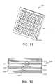
- the efficiency of the lasercan be improved using an active region design as depicted in FIG. 11 for the vertical cavity organic laser structure.
- the organic active regionincludes one or more lasing elements 200 .
- periodic gain layers 305are aligned with the antinodes of the device's standing wave electromagnetic field, where the laser's standing electromagnetic field pattern 320 in the lasing elements 200 is schematically shown. Since stimulated emission is highest at the antinodes and negligible at the nodes of the electromagnetic field, it is inherently advantageous to form the periodic gain layers 305 as shown in FIG. 12 , separated by organic spacer layers 310 .
- the organic spacer layers 310do not undergo stimulated or spontaneous emission and largely do not absorb either the laser light 122 or the pump beam OLED light 120 wavelengths.
- An example of a material suitable for forming an organic spacer layer 310is the organic material 1,1-Bis-(4-bis(4-methyl-phenyl)-amino-phenyl)-cyclohexane (TAPC).
- TAPCworks well as the spacer material since it largely does not absorb either the laser output or the pump beam energy and, in addition, its refractive index is slightly lower than that of most organic host materials. This refractive index difference is useful since it helps in maximizing the overlap between the electromagnetic field antinodes and the periodic gain layers 305 . As will be discussed below with reference to the present invention, employing periodic gain region(s) instead of a bulk gain region results in higher power conversion efficiencies and a significant reduction of the unwanted spontaneous emission.
- the placement of the gain region(s)is determined by using the standard matrix method of optics; see Corzine et al., Design of Fabry-Perot Surface-Emitting Lasers with a Periodic Gain Structure, IEEE Journal of Quantum Electronics, Vol. 25, No. 6, June 1989, pp. 1513–1524. To get good results, the thicknesses of the periodic gain layer(s) 305 need to be at or below 50 nm in order to avoid unwanted spontaneous emission.
- the lasercan be increased in area while maintaining a degree of spatial coherence by utilizing the phase locked organic laser array 220 as depicted in FIG. 11 .
- phase locked organic laser array 220lasing elements 200 separated by inter element regions 210 need to be defined on the surface of the organic laser 24 .
- intensity and phase informationmust be exchanged amongst the lasing elements 200 . This is best obtained by weakly confining the laser emissions to the lasing regions by either small amounts of built in index or gain guiding, e.g. by modulating the reflectance of one of the mirrors.
- the reflectance modulationis affected by patterning and forming an etched region in the bottom dielectric stack, using standard photolithographic and etching techniques, thus forming a two dimensional array of lasing elements 200 in the form of circular pillars on the surface of the bottom dielectric stack.
- the remainder of the organic laser micro cavity structureis deposited upon the patterned bottom dielectric stack as described above.
- the shape of the lasing elements 200is circular; however, other shapes are possible, such as rectangular.
- the inter-element spacing 210is in the range of 0.25 to 4 ⁇ m.
- the etch depthis preferred to be from 200 to 1000 nm deep.
Landscapes
- Engineering & Computer Science (AREA)
- General Engineering & Computer Science (AREA)
- Theoretical Computer Science (AREA)
- Human Computer Interaction (AREA)
- Physics & Mathematics (AREA)
- General Physics & Mathematics (AREA)
- Mechanical Engineering (AREA)
- Electroluminescent Light Sources (AREA)
- Position Input By Displaying (AREA)
- Devices For Indicating Variable Information By Combining Individual Elements (AREA)
Abstract
Description
- 10 substrate
- 12 encapsulating cover
- 14 OLED display
- 16 emitted light
- 20 OLED laser light emitter
- 22 OLED
- 24 organic laser
- 26 light sensor
- 28 optics
- 30 controller
- 32 enclosure
- 34 light pipe
- 100 electrode
- 102 transport layer
- 104 emissive layer
- 106 transport layer
- 108 electrode layer
- 110 transparent planarization layer
- 112 mirror
- 114 active layer
- 116 mirror
- 120 incoherent light
- 122 laser light
- 200 laser element
- 210 inter element spacing
- 220 laser array
- 305 periodic gain layer
- 310 spacer layer
- 320 standing wave pattern
Claims (21)
Priority Applications (6)
| Application Number | Priority Date | Filing Date | Title |
|---|---|---|---|
| US10/422,458US7133032B2 (en) | 2003-04-24 | 2003-04-24 | OLED display and touch screen |
| EP04076139AEP1471459A3 (en) | 2003-04-24 | 2004-04-13 | Organic LED display and touch screen |
| JP2004125464AJP2004326786A (en) | 2003-04-24 | 2004-04-21 | OLED display / touch screen system |
| CNA2004100350980ACN1540603A (en) | 2003-04-24 | 2004-04-23 | OLED displays and touch screens |
| TW093111505ATWI341483B (en) | 2003-04-24 | 2004-04-23 | Oled display and touch screen |
| KR1020040028381AKR20040093041A (en) | 2003-04-24 | 2004-04-23 | Oled display and touch screen |
Applications Claiming Priority (1)
| Application Number | Priority Date | Filing Date | Title |
|---|---|---|---|
| US10/422,458US7133032B2 (en) | 2003-04-24 | 2003-04-24 | OLED display and touch screen |
Publications (2)
| Publication Number | Publication Date |
|---|---|
| US20040212603A1 US20040212603A1 (en) | 2004-10-28 |
| US7133032B2true US7133032B2 (en) | 2006-11-07 |
Family
ID=32962442
Family Applications (1)
| Application Number | Title | Priority Date | Filing Date |
|---|---|---|---|
| US10/422,458Expired - LifetimeUS7133032B2 (en) | 2003-04-24 | 2003-04-24 | OLED display and touch screen |
Country Status (6)
| Country | Link |
|---|---|
| US (1) | US7133032B2 (en) |
| EP (1) | EP1471459A3 (en) |
| JP (1) | JP2004326786A (en) |
| KR (1) | KR20040093041A (en) |
| CN (1) | CN1540603A (en) |
| TW (1) | TWI341483B (en) |
Cited By (87)
| Publication number | Priority date | Publication date | Assignee | Title |
|---|---|---|---|---|
| US20050093466A1 (en)* | 2003-09-30 | 2005-05-05 | Sanyo Electric Co., Ltd. | Electroluminescent display device |
| US20070033903A1 (en)* | 2005-08-15 | 2007-02-15 | Uhlmann Pac-Systeme Gmbh & Co. Kg | Packaging machine |
| US20070208435A1 (en)* | 2006-03-06 | 2007-09-06 | Siemens Aktiengesellschaft | Assembly for an automation system |
| US20070283832A1 (en)* | 2006-06-09 | 2007-12-13 | Apple Computer, Inc. | Imprint circuit patterning |
| US20080158167A1 (en)* | 2007-01-03 | 2008-07-03 | Apple Computer, Inc. | Simultaneous sensing arrangement |
| US20090189878A1 (en)* | 2004-04-29 | 2009-07-30 | Neonode Inc. | Light-based touch screen |
| US20090214072A1 (en)* | 2007-06-17 | 2009-08-27 | Personics Holdings Inc. | Earpiece Sealing System |
| US20090256812A1 (en)* | 2008-04-15 | 2009-10-15 | Samsung Electronics Co., Ltd. | Display apparatus and control method of the same |
| US20090322708A1 (en)* | 2008-06-30 | 2009-12-31 | International Business Machines Corporation | Optical Touch Panel Having SMT Components As Optical Gates |
| US20100001973A1 (en)* | 2008-07-03 | 2010-01-07 | Apple Inc. | Display with dual-function capacitive elements |
| US20100026645A1 (en)* | 2008-07-29 | 2010-02-04 | Sang-Hoon Yim | Touch display panel |
| US20100045634A1 (en)* | 2008-08-21 | 2010-02-25 | Tpk Touch Solutions Inc. | Optical diode laser touch-control device |
| KR100947283B1 (en) | 2008-02-28 | 2010-03-16 | (주)디지텍시스템스 | Infrared touch screen with 3D operation |
| US20100110041A1 (en)* | 2008-07-11 | 2010-05-06 | Brent Jang | Organic light emitting display device |
| US20100123866A1 (en)* | 2008-11-18 | 2010-05-20 | Shih Chang Chang | Common Bus Design for a TFT-LCD Display |
| US20100144391A1 (en)* | 2008-12-05 | 2010-06-10 | Shih Chang Chang | Integrated touch panel for a TFT display |
| US7804441B1 (en)* | 2007-07-13 | 2010-09-28 | The United States Of America As Represented By The Secretary Of The Navy | Detection of concealed object by standing waves |
| US20100265207A1 (en)* | 2009-04-21 | 2010-10-21 | Industrial Technology Research Institute | Touch-sensing display apparatus and fabricating method thereof |
| US20100265206A1 (en)* | 2009-04-21 | 2010-10-21 | Industrial Technology Research Institute | Touch-sensing display apparatus and fabricating method thereof |
| US20100321344A1 (en)* | 2009-06-23 | 2010-12-23 | Meng-Shin Yen | Optical touch system and operating method thereof |
| US20110032209A1 (en)* | 2009-08-06 | 2011-02-10 | Samsung Mobile Display Co. Ltd. | Display apparatus |
| US20110043485A1 (en)* | 2007-07-06 | 2011-02-24 | Neonode Inc. | Scanning of a touch screen |
| US20110167628A1 (en)* | 2002-12-10 | 2011-07-14 | Neonode, Inc. | Component bonding using a capillary effect |
| US20110175852A1 (en)* | 2002-11-04 | 2011-07-21 | Neonode, Inc. | Light-based touch screen using elliptical and parabolic reflectors |
| US7995041B2 (en) | 2009-02-02 | 2011-08-09 | Apple Inc. | Integrated touch screen |
| US20110210946A1 (en)* | 2002-12-10 | 2011-09-01 | Neonode, Inc. | Light-based touch screen using elongated light guides |
| US20110298752A1 (en)* | 2010-06-02 | 2011-12-08 | Hon Hai Precision Industry Co., Ltd. | Electronic device with infrared touch input function |
| US8115753B2 (en) | 2007-04-11 | 2012-02-14 | Next Holdings Limited | Touch screen system with hover and click input methods |
| US8149221B2 (en) | 2004-05-07 | 2012-04-03 | Next Holdings Limited | Touch panel display system with illumination and detection provided from a single edge |
| US8217913B2 (en) | 2009-02-02 | 2012-07-10 | Apple Inc. | Integrated touch screen |
| US8243027B2 (en) | 2006-06-09 | 2012-08-14 | Apple Inc. | Touch screen liquid crystal display |
| US20120218229A1 (en)* | 2008-08-07 | 2012-08-30 | Rapt Ip Limited | Detecting Multitouch Events in an Optical Touch-Sensitive Device Using Touch Event Templates |
| US8289299B2 (en) | 2003-02-14 | 2012-10-16 | Next Holdings Limited | Touch screen signal processing |
| US8384693B2 (en)* | 2007-08-30 | 2013-02-26 | Next Holdings Limited | Low profile touch panel systems |
| US8405637B2 (en) | 2008-01-07 | 2013-03-26 | Next Holdings Limited | Optical position sensing system and optical position sensor assembly with convex imaging window |
| US8416209B2 (en) | 2004-05-06 | 2013-04-09 | Apple Inc. | Multipoint touchscreen |
| US8416217B1 (en) | 2002-11-04 | 2013-04-09 | Neonode Inc. | Light-based finger gesture user interface |
| TWI394070B (en)* | 2009-07-22 | 2013-04-21 | Arima Lasers Corp | Optical device |
| US8432377B2 (en) | 2007-08-30 | 2013-04-30 | Next Holdings Limited | Optical touchscreen with improved illumination |
| US8432371B2 (en) | 2006-06-09 | 2013-04-30 | Apple Inc. | Touch screen liquid crystal display |
| US8456447B2 (en) | 2003-02-14 | 2013-06-04 | Next Holdings Limited | Touch screen signal processing |
| US8493330B2 (en) | 2007-01-03 | 2013-07-23 | Apple Inc. | Individual channel phase delay scheme |
| US8508508B2 (en) | 2003-02-14 | 2013-08-13 | Next Holdings Limited | Touch screen signal processing with single-point calibration |
| US8654083B2 (en) | 2006-06-09 | 2014-02-18 | Apple Inc. | Touch screen liquid crystal display |
| US8674966B2 (en) | 2001-11-02 | 2014-03-18 | Neonode Inc. | ASIC controller for light-based touch screen |
| US8743300B2 (en) | 2010-12-22 | 2014-06-03 | Apple Inc. | Integrated touch screens |
| US8775023B2 (en) | 2009-02-15 | 2014-07-08 | Neanode Inc. | Light-based touch controls on a steering wheel and dashboard |
| US20140225098A1 (en)* | 2011-10-17 | 2014-08-14 | Lg Chem, Ltd. | Substrate for organic electronic device |
| US8896575B2 (en) | 2002-11-04 | 2014-11-25 | Neonode Inc. | Pressure-sensitive touch screen |
| US8902196B2 (en) | 2002-12-10 | 2014-12-02 | Neonode Inc. | Methods for determining a touch location on a touch screen |
| US9052771B2 (en) | 2002-11-04 | 2015-06-09 | Neonode Inc. | Touch screen calibration and update methods |
| US9052777B2 (en) | 2001-11-02 | 2015-06-09 | Neonode Inc. | Optical elements with alternating reflective lens facets |
| US9063614B2 (en) | 2009-02-15 | 2015-06-23 | Neonode Inc. | Optical touch screens |
| US9069124B2 (en)* | 2009-07-16 | 2015-06-30 | O-Net Wavetouch Limited | Device, a system and a method of encoding a position of an object |
| US9092093B2 (en) | 2012-11-27 | 2015-07-28 | Neonode Inc. | Steering wheel user interface |
| US20150277666A1 (en)* | 2001-11-02 | 2015-10-01 | Neonode Inc. | Asic controller for light-based sensor |
| US9195344B2 (en) | 2002-12-10 | 2015-11-24 | Neonode Inc. | Optical surface using a reflected image for determining three-dimensional position information |
| US9207800B1 (en) | 2014-09-23 | 2015-12-08 | Neonode Inc. | Integrated light guide and touch screen frame and multi-touch determination method |
| US9213443B2 (en) | 2009-02-15 | 2015-12-15 | Neonode Inc. | Optical touch screen systems using reflected light |
| US9342176B2 (en) | 2008-07-21 | 2016-05-17 | Samsung Display Co., Ltd. | Organic light emitting display device |
| US9367188B2 (en) | 2014-05-23 | 2016-06-14 | Apple Inc. | RC matching in a touch screen |
| US9395583B2 (en) | 2012-06-06 | 2016-07-19 | Apple Inc. | Column spacer design for a display incorporating a third metal layer |
| WO2016132180A1 (en) | 2015-02-20 | 2016-08-25 | Tubitak | Thienothiophene and dithienothiophene - boron (donor-acceptor) based materials for organic light emitting diodes |
| WO2016132179A1 (en) | 2015-02-20 | 2016-08-25 | Tubitak | Thienothiophene/dithienothiophene - triphenylamine/tetraphenylethylene derivatives for organic light emitting diodes |
| US9471170B2 (en) | 2002-11-04 | 2016-10-18 | Neonode Inc. | Light-based touch screen with shift-aligned emitter and receiver lenses |
| TWI565117B (en)* | 2015-06-10 | 2017-01-01 | Wisechip Semiconductor Inc | Organic light emitting diode module with optical signal transmission |
| US9606663B2 (en) | 2008-09-10 | 2017-03-28 | Apple Inc. | Multiple stimulation phase determination |
| US9710095B2 (en) | 2007-01-05 | 2017-07-18 | Apple Inc. | Touch screen stack-ups |
| US9715306B2 (en) | 2008-09-10 | 2017-07-25 | Apple Inc. | Single chip multi-stimulus sensor controller |
| US9778500B2 (en) | 2009-10-28 | 2017-10-03 | E Ink Corporation | Electro-optic displays with touch sensors and/or tactile feedback |
| US9990084B2 (en) | 2007-06-13 | 2018-06-05 | Apple Inc. | Touch detection using multiple simultaneous stimulation signals |
| US10019103B2 (en) | 2013-02-13 | 2018-07-10 | Apple Inc. | In-cell touch for LED |
| US10042476B2 (en) | 2008-09-10 | 2018-08-07 | Apple Inc. | Channel scan architecture for multiple stimulus multi-touch sensor panels |
| US20180331302A1 (en)* | 2017-03-16 | 2018-11-15 | Wuhan China Star Optoelectronics Technology Co., Ltd. | Organic light emitting device and preparation method thereof |
| US10133382B2 (en) | 2014-05-16 | 2018-11-20 | Apple Inc. | Structure for integrated touch screen |
| US10209813B2 (en) | 2013-12-13 | 2019-02-19 | Apple Inc. | Integrated touch and display architectures for self-capacitive touch sensors |
| US10268295B2 (en) | 2014-04-16 | 2019-04-23 | Apple Inc. | Structure for pixelated self-capacitance |
| US10282034B2 (en) | 2012-10-14 | 2019-05-07 | Neonode Inc. | Touch sensitive curved and flexible displays |
| US10852876B2 (en) | 2014-05-28 | 2020-12-01 | Apple Inc. | Narrow border touch screen |
| US11379048B2 (en) | 2012-10-14 | 2022-07-05 | Neonode Inc. | Contactless control panel |
| US11429230B2 (en) | 2018-11-28 | 2022-08-30 | Neonode Inc | Motorist user interface sensor |
| US11475699B2 (en) | 2020-01-22 | 2022-10-18 | Asti Global Inc., Taiwan | Display module and image display thereof |
| US11508789B2 (en) | 2020-05-20 | 2022-11-22 | Samsung Display Co., Ltd. | Display device and method of manufacturing the same |
| US11669210B2 (en) | 2020-09-30 | 2023-06-06 | Neonode Inc. | Optical touch sensor |
| US11733808B2 (en) | 2012-10-14 | 2023-08-22 | Neonode, Inc. | Object detector based on reflected light |
| US11842014B2 (en) | 2019-12-31 | 2023-12-12 | Neonode Inc. | Contactless touch input system |
| US12032817B2 (en) | 2012-11-27 | 2024-07-09 | Neonode Inc. | Vehicle user interface |
Families Citing this family (99)
| Publication number | Priority date | Publication date | Assignee | Title |
|---|---|---|---|---|
| US6803906B1 (en) | 2000-07-05 | 2004-10-12 | Smart Technologies, Inc. | Passive touch system and method of detecting user input |
| US6954197B2 (en) | 2002-11-15 | 2005-10-11 | Smart Technologies Inc. | Size/scale and orientation determination of a pointer in a camera-based touch system |
| US7042444B2 (en)* | 2003-01-17 | 2006-05-09 | Eastman Kodak Company | OLED display and touch screen |
| US7532206B2 (en) | 2003-03-11 | 2009-05-12 | Smart Technologies Ulc | System and method for differentiating between pointers used to contact touch surface |
| US6939012B2 (en)* | 2003-06-02 | 2005-09-06 | Eastman Kodak Company | Laser image projector |
| JP2005038729A (en)* | 2003-07-16 | 2005-02-10 | Sanyo Electric Co Ltd | EL display device |
| US7411575B2 (en) | 2003-09-16 | 2008-08-12 | Smart Technologies Ulc | Gesture recognition method and touch system incorporating the same |
| US7274356B2 (en) | 2003-10-09 | 2007-09-25 | Smart Technologies Inc. | Apparatus for determining the location of a pointer within a region of interest |
| US6885157B1 (en)* | 2003-11-25 | 2005-04-26 | Eastman Kodak Company | Integrated touch screen and OLED flat-panel display |
| JP2005173881A (en)* | 2003-12-10 | 2005-06-30 | Sanyo Electric Co Ltd | EL display device |
| US7355593B2 (en) | 2004-01-02 | 2008-04-08 | Smart Technologies, Inc. | Pointer tracking across multiple overlapping coordinate input sub-regions defining a generally contiguous input region |
| TW200620181A (en)* | 2004-12-01 | 2006-06-16 | Chi Lin Technology Co Ltd | Brightness control device and method of intelligent display panel |
| US7460110B2 (en) | 2004-04-29 | 2008-12-02 | Smart Technologies Ulc | Dual mode touch system |
| US8120596B2 (en) | 2004-05-21 | 2012-02-21 | Smart Technologies Ulc | Tiled touch system |
| US8184108B2 (en)* | 2004-06-30 | 2012-05-22 | Poa Sana Liquidating Trust | Apparatus and method for a folded optical element waveguide for use with light based touch screens |
| KR100616744B1 (en) | 2005-02-25 | 2006-08-28 | (주)모비솔 | Pointing device using holographic optical element |
| JP4837295B2 (en) | 2005-03-02 | 2011-12-14 | 株式会社沖データ | Semiconductor device, LED device, LED head, and image forming apparatus |
| ES2318950B1 (en)* | 2006-03-27 | 2009-12-17 | Universidad De Alcala | TRANSCUTANEOUS LASER THERAPY APPLIANCE USING AN ORGANIC LIGHT EMISSION DEVICE. |
| TWI321288B (en)* | 2006-08-31 | 2010-03-01 | Egalax Empia Technology Inc | Apparatus and method for detecting position, and touch panel using the same |
| US7874923B2 (en) | 2006-09-27 | 2011-01-25 | Igt | Multiple touchscreen sensors on a monolithic structure |
| US9442607B2 (en) | 2006-12-04 | 2016-09-13 | Smart Technologies Inc. | Interactive input system and method |
| US8094137B2 (en) | 2007-07-23 | 2012-01-10 | Smart Technologies Ulc | System and method of detecting contact on a display |
| EP2034287A1 (en)* | 2007-09-10 | 2009-03-11 | Nederlandse Organisatie voor Toegepast-Natuuurwetenschappelijk Onderzoek TNO | Optical sensor for measuring a force distribution |
| EP2068212A1 (en) | 2007-12-06 | 2009-06-10 | The Swatch Group Research and Development Ltd. | Portable object such as a timepiece comprising means for triggering an electronic control function |
| KR100941280B1 (en)* | 2008-01-24 | 2010-02-11 | 엘지이노텍 주식회사 | Display |
| TWI479714B (en)* | 2008-01-29 | 2015-04-01 | Koninkl Philips Electronics Nv | Organic light emitting diode lighting device with integrated proximity sensor |
| JP5166920B2 (en)* | 2008-03-10 | 2013-03-21 | ローム株式会社 | Display device |
| US20090256811A1 (en)* | 2008-04-15 | 2009-10-15 | Sony Ericsson Mobile Communications Ab | Optical touch screen |
| US8902193B2 (en) | 2008-05-09 | 2014-12-02 | Smart Technologies Ulc | Interactive input system and bezel therefor |
| EP2305007B1 (en)* | 2008-07-08 | 2012-12-12 | Koninklijke Philips Electronics N.V. | Methods and apparatus for determining relative positions of led lighting units |
| US8339378B2 (en) | 2008-11-05 | 2012-12-25 | Smart Technologies Ulc | Interactive input system with multi-angle reflector |
| US8294691B2 (en)* | 2008-11-14 | 2012-10-23 | Motorola Mobility Llc | Waveguard touch panel |
| SE533704C2 (en) | 2008-12-05 | 2010-12-07 | Flatfrog Lab Ab | Touch sensitive apparatus and method for operating the same |
| TWM363032U (en)* | 2009-02-25 | 2009-08-11 | Pixart Imaging Inc | Optical touch control module |
| TWM371272U (en)* | 2009-04-01 | 2009-12-21 | Pixart Imaging Inc | Optical touch control module |
| US8624849B2 (en)* | 2009-04-20 | 2014-01-07 | Apple Inc. | Touch actuated sensor configuration integrated with an OLED structure |
| US20110001706A1 (en)* | 2009-07-02 | 2011-01-06 | Emery Sanford | Electronic device touch screen display module |
| KR101024069B1 (en)* | 2009-08-13 | 2011-03-22 | 주성엔지니어링(주) | Organic electroluminescent devices |
| US8072437B2 (en)* | 2009-08-26 | 2011-12-06 | Global Oled Technology Llc | Flexible multitouch electroluminescent display |
| US20110095989A1 (en)* | 2009-10-23 | 2011-04-28 | Smart Technologies Ulc | Interactive input system and bezel therefor |
| EP2322345A1 (en) | 2009-11-06 | 2011-05-18 | Bayer MaterialScience AG | Laminated structure with electric and/or electronic function elements |
| FR2960058B1 (en)* | 2010-05-12 | 2012-06-15 | Pi Corporate | NON-CONTACT MOTION SENSOR WITH PHOTOELECTRIC EFFECT AND DEVICE USING SUCH SENSOR |
| US20110285643A1 (en)* | 2010-05-22 | 2011-11-24 | Pixart Imaging Inc. | Optical touch display device |
| CN102270069B (en) | 2010-06-03 | 2015-01-28 | 乐金显示有限公司 | Touch panel integrated display device |
| KR101901241B1 (en)* | 2010-06-03 | 2018-09-27 | 엘지디스플레이 주식회사 | Touch Panel Integrated Display Device |
| US8541856B2 (en)* | 2010-12-08 | 2013-09-24 | Omnivision Technologies, Inc. | Optical touch-screen imager |
| KR20120080845A (en) | 2011-01-10 | 2012-07-18 | 삼성전자주식회사 | Oled display apparatus having optical sensing funtion |
| US8963886B2 (en) | 2011-07-13 | 2015-02-24 | Flatfrog Laboratories Ab | Touch-sensing display panel |
| US8884900B2 (en) | 2011-07-13 | 2014-11-11 | Flatfrog Laboratories Ab | Touch-sensing display apparatus and electronic device therewith |
| US9092094B1 (en)* | 2011-09-22 | 2015-07-28 | Amazon Technologies, Inc. | Optical edge touch sensor |
| TWI563437B (en)* | 2011-09-26 | 2016-12-21 | Egalax Empia Technology Inc | Apparatus for detecting position by infrared rays and touch panel using the same |
| CN103827792A (en)* | 2011-09-29 | 2014-05-28 | 英特尔公司 | Optical fiber proximity sensor |
| JP5809117B2 (en)* | 2011-10-05 | 2015-11-10 | 富士フイルム株式会社 | Conductive sheet, touch panel, display device |
| US9207810B1 (en) | 2011-11-15 | 2015-12-08 | Amazon Technologies, Inc. | Fiber-optic touch sensor |
| TWI451312B (en)* | 2011-12-19 | 2014-09-01 | Pixart Imaging Inc | Optical touch device and light source assembly |
| GB2498716A (en)* | 2012-01-22 | 2013-07-31 | Alexander James Miles | A Control Panel for an Electronic Display |
| US9696751B2 (en)* | 2012-05-17 | 2017-07-04 | Kaneka Corporation | Substrate with transparent electrode, method for manufacturing same, and touch panel |
| US10168835B2 (en) | 2012-05-23 | 2019-01-01 | Flatfrog Laboratories Ab | Spatial resolution in touch displays |
| US9857916B2 (en)* | 2012-07-24 | 2018-01-02 | Flatfrog Laboratories Ab | Optical coupling in touch-sensing systems using diffusively transmitting element |
| CN103576992B (en)* | 2012-08-06 | 2017-09-15 | 原相科技股份有限公司 | Film and light guide plate and position detection system with positional information |
| TWI489350B (en)* | 2012-10-01 | 2015-06-21 | 原相科技股份有限公司 | Optical touch apparatus and image capturing apparatus |
| WO2014098740A1 (en)* | 2012-12-17 | 2014-06-26 | Flatfrog Laboratories Ab | Optical coupling of light into touch-sensing systems |
| WO2014112904A1 (en)* | 2013-01-16 | 2014-07-24 | Flatfrog Laboratories Ab | Touch-sensing display panel |
| WO2014112913A1 (en) | 2013-01-16 | 2014-07-24 | Flatfrog Laboratories Ab | Touch-sensing display panel |
| US20140267166A1 (en)* | 2013-03-12 | 2014-09-18 | Qualcomm Mems Technologies, Inc. | Combined optical touch and gesture sensing |
| US10019113B2 (en) | 2013-04-11 | 2018-07-10 | Flatfrog Laboratories Ab | Tomographic processing for touch detection |
| WO2015005847A1 (en) | 2013-07-12 | 2015-01-15 | Flatfrog Laboratories Ab | Partial detect mode |
| US10146376B2 (en) | 2014-01-16 | 2018-12-04 | Flatfrog Laboratories Ab | Light coupling in TIR-based optical touch systems |
| WO2015108480A1 (en) | 2014-01-16 | 2015-07-23 | Flatfrog Laboratories Ab | Improvements in tir-based optical touch systems of projection-type |
| EP3161594A4 (en) | 2014-06-27 | 2018-01-17 | FlatFrog Laboratories AB | Detection of surface contamination |
| US9652082B1 (en)* | 2014-08-20 | 2017-05-16 | Amazon Technologies, Inc. | Space efficient electronic device component configurations |
| KR102246296B1 (en)* | 2014-12-19 | 2021-04-30 | 삼성디스플레이 주식회사 | Display device |
| EP3250993B1 (en) | 2015-01-28 | 2019-09-04 | FlatFrog Laboratories AB | Dynamic touch quarantine frames |
| US10318074B2 (en) | 2015-01-30 | 2019-06-11 | Flatfrog Laboratories Ab | Touch-sensing OLED display with tilted emitters |
| US10496227B2 (en) | 2015-02-09 | 2019-12-03 | Flatfrog Laboratories Ab | Optical touch system comprising means for projecting and detecting light beams above and inside a transmissive panel |
| US10401546B2 (en) | 2015-03-02 | 2019-09-03 | Flatfrog Laboratories Ab | Optical component for light coupling |
| KR102497784B1 (en)* | 2015-10-06 | 2023-02-09 | 삼성디스플레이 주식회사 | Display device |
| EP4075246B1 (en) | 2015-12-09 | 2024-07-03 | FlatFrog Laboratories AB | Stylus for optical touch system |
| CN105468199B (en)* | 2015-12-26 | 2019-01-15 | 宸鸿科技(厦门)有限公司 | A kind of panel with pressure-sensing |
| KR101715773B1 (en)* | 2016-05-26 | 2017-03-14 | 주식회사 아하정보통신 | Display including touch sensor and touch sensing method using the same |
| EP3545392A4 (en) | 2016-11-24 | 2020-07-29 | FlatFrog Laboratories AB | AUTOMATIC OPTIMIZATION OF TOUCH SIGNALS |
| KR20250020732A (en) | 2016-12-07 | 2025-02-11 | 플라트프로그 라보라토리즈 에이비 | An improved touch device |
| CN110300950B (en) | 2017-02-06 | 2023-06-16 | 平蛙实验室股份公司 | Optical coupling in touch sensing systems |
| US10606414B2 (en) | 2017-03-22 | 2020-03-31 | Flatfrog Laboratories Ab | Eraser for touch displays |
| WO2018175857A1 (en)* | 2017-03-23 | 2018-09-27 | Red Bank Technologies Llc | Head-mounted and head-up displays utilizing organic light emitting diodes that emit by stimulated emission |
| EP4036697A1 (en) | 2017-03-28 | 2022-08-03 | FlatFrog Laboratories AB | Optical touch sensing apparatus |
| US11256371B2 (en) | 2017-09-01 | 2022-02-22 | Flatfrog Laboratories Ab | Optical component |
| CN108110036A (en)* | 2017-12-15 | 2018-06-01 | 京东方科技集团股份有限公司 | OLED touch panels and its manufacturing method |
| WO2019172826A1 (en) | 2018-03-05 | 2019-09-12 | Flatfrog Laboratories Ab | Improved touch-sensing apparatus |
| WO2019226090A1 (en)* | 2018-05-24 | 2019-11-28 | Flatfrog Laboratories Ab | Frame for a touch-sensitive device and film application tool therefor |
| WO2020080992A1 (en) | 2018-10-20 | 2020-04-23 | Flatfrog Laboratories Ab | Frame for a touch-sensitive device and tool therefor |
| CN109508119B (en)* | 2018-12-21 | 2020-06-30 | 武汉华星光电半导体显示技术有限公司 | Floating touch display device and floating touch method |
| WO2020153890A1 (en) | 2019-01-25 | 2020-07-30 | Flatfrog Laboratories Ab | A videoconferencing terminal and method of operating the same |
| ES2991658T3 (en) | 2019-11-25 | 2024-12-04 | Flatfrog Lab Ab | A touch device |
| TWI812358B (en)* | 2020-01-22 | 2023-08-11 | 台灣愛司帝科技股份有限公司 | Display module and image display device thereof |
| US12282653B2 (en) | 2020-02-08 | 2025-04-22 | Flatfrog Laboratories Ab | Touch apparatus with low latency interactions |
| US11893189B2 (en)* | 2020-02-10 | 2024-02-06 | Flatfrog Laboratories Ab | Touch-sensing apparatus |
| EP4352599A4 (en)* | 2021-06-11 | 2025-08-20 | Flatfrog Lab Ab | TOUCH-SENSITIVE DISPLAY AND TOUCH-SENSITIVE DEVICE |
| CN219831802U (en)* | 2023-03-16 | 2023-10-13 | 深圳市天英联合科技股份有限公司 | Infrared touch screen |
Citations (8)
| Publication number | Priority date | Publication date | Assignee | Title |
|---|---|---|---|---|
| US4916308A (en)* | 1988-10-17 | 1990-04-10 | Tektronix, Inc. | Integrated liquid crystal display and optical touch panel |
| US6172459B1 (en) | 1998-07-28 | 2001-01-09 | Eastman Kodak Company | Electron-injecting layer providing a modified interface between an organic light-emitting structure and a cathode buffer layer |
| US20030150714A1 (en)* | 2002-02-08 | 2003-08-14 | Eastman Kodak Company | Method for manufacturing an integrated display device including an oled display and a touch screen |
| US20040090426A1 (en)* | 2002-11-07 | 2004-05-13 | Eastman Kodak Company | Transparent flexible sheet for resistive touch screen |
| US6762747B2 (en)* | 2000-09-20 | 2004-07-13 | Ricoh Company, Ltd. | Coordinate input detection device and method for electronic blackboard |
| US20040140961A1 (en)* | 2003-01-17 | 2004-07-22 | Eastman Kodak Company | Oled display and touch screen |
| US6846579B2 (en)* | 2002-02-15 | 2005-01-25 | Eastman Kodak Company | Multilayer with radiation absorber and touch screen |
| US6879319B2 (en)* | 2002-10-25 | 2005-04-12 | Eastman Kodak Company | Integrated OLED display and touch screen |
Family Cites Families (7)
| Publication number | Priority date | Publication date | Assignee | Title |
|---|---|---|---|---|
| JPS6465625A (en)* | 1987-09-07 | 1989-03-10 | Alps Electric Co Ltd | Optical type coordinate input device |
| GB2263765A (en)* | 1992-01-25 | 1993-08-04 | Paul Philip Oliver | Touch screen systems |
| TW244383B (en)* | 1993-10-22 | 1995-04-01 | Ibm | Touch-screen input device using the monitor as a light source operating at an intermediate frequency |
| JP3827450B2 (en)* | 1998-08-18 | 2006-09-27 | 富士通株式会社 | Optical scanning touch panel |
| WO2002082253A2 (en)* | 2001-04-04 | 2002-10-17 | Elo Touchsystems, Inc. | A touch input system |
| US20020186208A1 (en)* | 2001-05-15 | 2002-12-12 | Eastman Kodak Company | Organic electroluminescent display with integrated touch screen |
| US20030025738A1 (en)* | 2001-07-31 | 2003-02-06 | Eastman Kodak Company | User interface including portable display for use with multiple electronic devices |
- 2003
- 2003-04-24USUS10/422,458patent/US7133032B2/ennot_activeExpired - Lifetime
- 2004
- 2004-04-13EPEP04076139Apatent/EP1471459A3/ennot_activeWithdrawn
- 2004-04-21JPJP2004125464Apatent/JP2004326786A/enactivePending
- 2004-04-23CNCNA2004100350980Apatent/CN1540603A/enactivePending
- 2004-04-23KRKR1020040028381Apatent/KR20040093041A/ennot_activeWithdrawn
- 2004-04-23TWTW093111505Apatent/TWI341483B/ennot_activeIP Right Cessation
Patent Citations (9)
| Publication number | Priority date | Publication date | Assignee | Title |
|---|---|---|---|---|
| US4916308A (en)* | 1988-10-17 | 1990-04-10 | Tektronix, Inc. | Integrated liquid crystal display and optical touch panel |
| US6172459B1 (en) | 1998-07-28 | 2001-01-09 | Eastman Kodak Company | Electron-injecting layer providing a modified interface between an organic light-emitting structure and a cathode buffer layer |
| US6762747B2 (en)* | 2000-09-20 | 2004-07-13 | Ricoh Company, Ltd. | Coordinate input detection device and method for electronic blackboard |
| US20030150714A1 (en)* | 2002-02-08 | 2003-08-14 | Eastman Kodak Company | Method for manufacturing an integrated display device including an oled display and a touch screen |
| US6846579B2 (en)* | 2002-02-15 | 2005-01-25 | Eastman Kodak Company | Multilayer with radiation absorber and touch screen |
| US6879319B2 (en)* | 2002-10-25 | 2005-04-12 | Eastman Kodak Company | Integrated OLED display and touch screen |
| US20040090426A1 (en)* | 2002-11-07 | 2004-05-13 | Eastman Kodak Company | Transparent flexible sheet for resistive touch screen |
| US20040140961A1 (en)* | 2003-01-17 | 2004-07-22 | Eastman Kodak Company | Oled display and touch screen |
| US20040140960A1 (en)* | 2003-01-17 | 2004-07-22 | Eastman Kodak Company | OLED display and touch screen |
Non-Patent Citations (1)
| Title |
|---|
| Corzine et al., Design of Fabry-Perot Surface-Emitting Lasers with a Periodic Gain Structure, IEEE Journal of Quantum Electronics, vol. 25, No. 6, Jun. 1989, pp. 1513-1524. |
Cited By (187)
| Publication number | Priority date | Publication date | Assignee | Title |
|---|---|---|---|---|
| US20150277666A1 (en)* | 2001-11-02 | 2015-10-01 | Neonode Inc. | Asic controller for light-based sensor |
| US9778794B2 (en)* | 2001-11-02 | 2017-10-03 | Neonode Inc. | Light-based touch screen |
| US8674966B2 (en) | 2001-11-02 | 2014-03-18 | Neonode Inc. | ASIC controller for light-based touch screen |
| US9035917B2 (en) | 2001-11-02 | 2015-05-19 | Neonode Inc. | ASIC controller for light-based sensor |
| US9052777B2 (en) | 2001-11-02 | 2015-06-09 | Neonode Inc. | Optical elements with alternating reflective lens facets |
| US8416217B1 (en) | 2002-11-04 | 2013-04-09 | Neonode Inc. | Light-based finger gesture user interface |
| US8884926B1 (en) | 2002-11-04 | 2014-11-11 | Neonode Inc. | Light-based finger gesture user interface |
| US20110175852A1 (en)* | 2002-11-04 | 2011-07-21 | Neonode, Inc. | Light-based touch screen using elliptical and parabolic reflectors |
| US9262074B2 (en) | 2002-11-04 | 2016-02-16 | Neonode, Inc. | Finger gesture user interface |
| US8587562B2 (en)* | 2002-11-04 | 2013-11-19 | Neonode Inc. | Light-based touch screen using elliptical and parabolic reflectors |
| US9052771B2 (en) | 2002-11-04 | 2015-06-09 | Neonode Inc. | Touch screen calibration and update methods |
| US9471170B2 (en) | 2002-11-04 | 2016-10-18 | Neonode Inc. | Light-based touch screen with shift-aligned emitter and receiver lenses |
| US8810551B2 (en) | 2002-11-04 | 2014-08-19 | Neonode Inc. | Finger gesture user interface |
| US8896575B2 (en) | 2002-11-04 | 2014-11-25 | Neonode Inc. | Pressure-sensitive touch screen |
| US20110210946A1 (en)* | 2002-12-10 | 2011-09-01 | Neonode, Inc. | Light-based touch screen using elongated light guides |
| US9195344B2 (en) | 2002-12-10 | 2015-11-24 | Neonode Inc. | Optical surface using a reflected image for determining three-dimensional position information |
| US9389730B2 (en) | 2002-12-10 | 2016-07-12 | Neonode Inc. | Light-based touch screen using elongated light guides |
| US8902196B2 (en) | 2002-12-10 | 2014-12-02 | Neonode Inc. | Methods for determining a touch location on a touch screen |
| US8403203B2 (en) | 2002-12-10 | 2013-03-26 | Neonoda Inc. | Component bonding using a capillary effect |
| US20110167628A1 (en)* | 2002-12-10 | 2011-07-14 | Neonode, Inc. | Component bonding using a capillary effect |
| US8508508B2 (en) | 2003-02-14 | 2013-08-13 | Next Holdings Limited | Touch screen signal processing with single-point calibration |
| US8466885B2 (en) | 2003-02-14 | 2013-06-18 | Next Holdings Limited | Touch screen signal processing |
| US8456447B2 (en) | 2003-02-14 | 2013-06-04 | Next Holdings Limited | Touch screen signal processing |
| US8289299B2 (en) | 2003-02-14 | 2012-10-16 | Next Holdings Limited | Touch screen signal processing |
| US7289088B2 (en)* | 2003-09-30 | 2007-10-30 | Sanyo Electric Co., Ltd. | Electroluminescent display device |
| US20050093466A1 (en)* | 2003-09-30 | 2005-05-05 | Sanyo Electric Co., Ltd. | Electroluminescent display device |
| US20090189878A1 (en)* | 2004-04-29 | 2009-07-30 | Neonode Inc. | Light-based touch screen |
| US8339379B2 (en) | 2004-04-29 | 2012-12-25 | Neonode Inc. | Light-based touch screen |
| US8416209B2 (en) | 2004-05-06 | 2013-04-09 | Apple Inc. | Multipoint touchscreen |
| US11604547B2 (en) | 2004-05-06 | 2023-03-14 | Apple Inc. | Multipoint touchscreen |
| US9454277B2 (en) | 2004-05-06 | 2016-09-27 | Apple Inc. | Multipoint touchscreen |
| US8605051B2 (en) | 2004-05-06 | 2013-12-10 | Apple Inc. | Multipoint touchscreen |
| US10331259B2 (en) | 2004-05-06 | 2019-06-25 | Apple Inc. | Multipoint touchscreen |
| US8872785B2 (en) | 2004-05-06 | 2014-10-28 | Apple Inc. | Multipoint touchscreen |
| US10908729B2 (en) | 2004-05-06 | 2021-02-02 | Apple Inc. | Multipoint touchscreen |
| US8928618B2 (en) | 2004-05-06 | 2015-01-06 | Apple Inc. | Multipoint touchscreen |
| US8982087B2 (en) | 2004-05-06 | 2015-03-17 | Apple Inc. | Multipoint touchscreen |
| US9035907B2 (en) | 2004-05-06 | 2015-05-19 | Apple Inc. | Multipoint touchscreen |
| US8149221B2 (en) | 2004-05-07 | 2012-04-03 | Next Holdings Limited | Touch panel display system with illumination and detection provided from a single edge |
| US20070033903A1 (en)* | 2005-08-15 | 2007-02-15 | Uhlmann Pac-Systeme Gmbh & Co. Kg | Packaging machine |
| US20070208435A1 (en)* | 2006-03-06 | 2007-09-06 | Siemens Aktiengesellschaft | Assembly for an automation system |
| US11175762B2 (en) | 2006-06-09 | 2021-11-16 | Apple Inc. | Touch screen liquid crystal display |
| US9575610B2 (en) | 2006-06-09 | 2017-02-21 | Apple Inc. | Touch screen liquid crystal display |
| US20070283832A1 (en)* | 2006-06-09 | 2007-12-13 | Apple Computer, Inc. | Imprint circuit patterning |
| US8552989B2 (en) | 2006-06-09 | 2013-10-08 | Apple Inc. | Integrated display and touch screen |
| US9244561B2 (en) | 2006-06-09 | 2016-01-26 | Apple Inc. | Touch screen liquid crystal display |
| US11886651B2 (en) | 2006-06-09 | 2024-01-30 | Apple Inc. | Touch screen liquid crystal display |
| US8654083B2 (en) | 2006-06-09 | 2014-02-18 | Apple Inc. | Touch screen liquid crystal display |
| US8243027B2 (en) | 2006-06-09 | 2012-08-14 | Apple Inc. | Touch screen liquid crystal display |
| US9268429B2 (en) | 2006-06-09 | 2016-02-23 | Apple Inc. | Integrated display and touch screen |
| US8432371B2 (en) | 2006-06-09 | 2013-04-30 | Apple Inc. | Touch screen liquid crystal display |
| US8451244B2 (en) | 2006-06-09 | 2013-05-28 | Apple Inc. | Segmented Vcom |
| US10976846B2 (en) | 2006-06-09 | 2021-04-13 | Apple Inc. | Touch screen liquid crystal display |
| US8259078B2 (en) | 2006-06-09 | 2012-09-04 | Apple Inc. | Touch screen liquid crystal display |
| US10191576B2 (en) | 2006-06-09 | 2019-01-29 | Apple Inc. | Touch screen liquid crystal display |
| US20080158167A1 (en)* | 2007-01-03 | 2008-07-03 | Apple Computer, Inc. | Simultaneous sensing arrangement |
| US8493330B2 (en) | 2007-01-03 | 2013-07-23 | Apple Inc. | Individual channel phase delay scheme |
| US8928617B2 (en) | 2007-01-03 | 2015-01-06 | Apple Inc. | Simultaneous sensing arrangement |
| US10871850B2 (en) | 2007-01-03 | 2020-12-22 | Apple Inc. | Simultaneous sensing arrangement |
| US7812827B2 (en) | 2007-01-03 | 2010-10-12 | Apple Inc. | Simultaneous sensing arrangement |
| US9552115B2 (en) | 2007-01-03 | 2017-01-24 | Apple Inc. | Simultaneous sensing arrangement |
| US20100328265A1 (en)* | 2007-01-03 | 2010-12-30 | Hotelling Steven P | Simultaneous sensing arrangement |
| US8552998B2 (en) | 2007-01-03 | 2013-10-08 | Apple Inc. | Simultaneous sensing arrangement |
| US11675454B2 (en) | 2007-01-03 | 2023-06-13 | Apple Inc. | Simultaneous sensing arrangement |
| US10521065B2 (en) | 2007-01-05 | 2019-12-31 | Apple Inc. | Touch screen stack-ups |
| US9710095B2 (en) | 2007-01-05 | 2017-07-18 | Apple Inc. | Touch screen stack-ups |
| US8115753B2 (en) | 2007-04-11 | 2012-02-14 | Next Holdings Limited | Touch screen system with hover and click input methods |
| US10747355B2 (en) | 2007-06-13 | 2020-08-18 | Apple Inc. | Touch detection using multiple simultaneous stimulation signals |
| US11775109B2 (en) | 2007-06-13 | 2023-10-03 | Apple Inc. | Touch detection using multiple simultaneous stimulation signals |
| US9990084B2 (en) | 2007-06-13 | 2018-06-05 | Apple Inc. | Touch detection using multiple simultaneous stimulation signals |
| US11106308B2 (en) | 2007-06-13 | 2021-08-31 | Apple Inc. | Touch detection using multiple simultaneous stimulation signals |
| US20090214072A1 (en)* | 2007-06-17 | 2009-08-27 | Personics Holdings Inc. | Earpiece Sealing System |
| US8471830B2 (en) | 2007-07-06 | 2013-06-25 | Neonode Inc. | Scanning of a touch screen |
| US20110043485A1 (en)* | 2007-07-06 | 2011-02-24 | Neonode Inc. | Scanning of a touch screen |
| US8174430B1 (en) | 2007-07-13 | 2012-05-08 | The United States Of America, As Represented By The Secretary Of The Navy | Detection of concealed object by standing waves |
| US7804441B1 (en)* | 2007-07-13 | 2010-09-28 | The United States Of America As Represented By The Secretary Of The Navy | Detection of concealed object by standing waves |
| US8384693B2 (en)* | 2007-08-30 | 2013-02-26 | Next Holdings Limited | Low profile touch panel systems |
| US8432377B2 (en) | 2007-08-30 | 2013-04-30 | Next Holdings Limited | Optical touchscreen with improved illumination |
| US8405636B2 (en) | 2008-01-07 | 2013-03-26 | Next Holdings Limited | Optical position sensing system and optical position sensor assembly |
| US8405637B2 (en) | 2008-01-07 | 2013-03-26 | Next Holdings Limited | Optical position sensing system and optical position sensor assembly with convex imaging window |
| KR100947283B1 (en) | 2008-02-28 | 2010-03-16 | (주)디지텍시스템스 | Infrared touch screen with 3D operation |
| US8542197B2 (en) | 2008-04-15 | 2013-09-24 | Samsung Electronics Co., Ltd. | Display apparatus and control method of the same |
| US20090256812A1 (en)* | 2008-04-15 | 2009-10-15 | Samsung Electronics Co., Ltd. | Display apparatus and control method of the same |
| US8643608B2 (en)* | 2008-06-30 | 2014-02-04 | International Business Machines Corporation | Optical touch panel having SMT components as optical gates |
| US20090322708A1 (en)* | 2008-06-30 | 2009-12-31 | International Business Machines Corporation | Optical Touch Panel Having SMT Components As Optical Gates |
| US9354761B2 (en) | 2008-07-03 | 2016-05-31 | Apple Inc. | Display with dual-function capacitive elements |
| US9075490B2 (en) | 2008-07-03 | 2015-07-07 | Apple Inc. | Display with dual-function capacitive elements |
| US8773397B2 (en) | 2008-07-03 | 2014-07-08 | Apple Inc. | Display with dual-function capacitive elements |
| US8743087B2 (en) | 2008-07-03 | 2014-06-03 | Apple Inc. | Display with dual-function capacitive elements |
| US20100001973A1 (en)* | 2008-07-03 | 2010-01-07 | Apple Inc. | Display with dual-function capacitive elements |
| US8508495B2 (en) | 2008-07-03 | 2013-08-13 | Apple Inc. | Display with dual-function capacitive elements |
| US10936132B2 (en) | 2008-07-11 | 2021-03-02 | Samsung Display Co., Ltd. | Organic light emitting display device |
| US8928597B2 (en) | 2008-07-11 | 2015-01-06 | Samsung Display Co., Ltd. | Organic light emitting display device |
| US20100110041A1 (en)* | 2008-07-11 | 2010-05-06 | Brent Jang | Organic light emitting display device |
| US9893126B2 (en) | 2008-07-11 | 2018-02-13 | Samsung Display Co., Ltd. | Organic light emitting display device |
| US9772709B2 (en) | 2008-07-21 | 2017-09-26 | Samsung Display Co., Ltd. | Organic light emitting display device |
| US9342176B2 (en) | 2008-07-21 | 2016-05-17 | Samsung Display Co., Ltd. | Organic light emitting display device |
| US20100026645A1 (en)* | 2008-07-29 | 2010-02-04 | Sang-Hoon Yim | Touch display panel |
| US9092092B2 (en)* | 2008-08-07 | 2015-07-28 | Rapt Ip Limited | Detecting multitouch events in an optical touch-sensitive device using touch event templates |
| US10795506B2 (en)* | 2008-08-07 | 2020-10-06 | Rapt Ip Limited | Detecting multitouch events in an optical touch- sensitive device using touch event templates |
| US20120218229A1 (en)* | 2008-08-07 | 2012-08-30 | Rapt Ip Limited | Detecting Multitouch Events in an Optical Touch-Sensitive Device Using Touch Event Templates |
| US20190163325A1 (en)* | 2008-08-07 | 2019-05-30 | Rapt Ip Limited | Detecting multitouch events in an optical touch-sensitive device using touch event templates |
| US9552104B2 (en) | 2008-08-07 | 2017-01-24 | Rapt Ip Limited | Detecting multitouch events in an optical touch-sensitive device using touch event templates |
| US10067609B2 (en) | 2008-08-07 | 2018-09-04 | Rapt Ip Limited | Detecting multitouch events in an optical touch-sensitive device using touch event templates |
| US20100045634A1 (en)* | 2008-08-21 | 2010-02-25 | Tpk Touch Solutions Inc. | Optical diode laser touch-control device |
| US10042472B2 (en) | 2008-09-10 | 2018-08-07 | Apple Inc. | Single-chip multi-stimulus sensor controller |
| US9715306B2 (en) | 2008-09-10 | 2017-07-25 | Apple Inc. | Single chip multi-stimulus sensor controller |
| US10042476B2 (en) | 2008-09-10 | 2018-08-07 | Apple Inc. | Channel scan architecture for multiple stimulus multi-touch sensor panels |
| US9606663B2 (en) | 2008-09-10 | 2017-03-28 | Apple Inc. | Multiple stimulation phase determination |
| US20100123866A1 (en)* | 2008-11-18 | 2010-05-20 | Shih Chang Chang | Common Bus Design for a TFT-LCD Display |
| US8294865B2 (en) | 2008-11-18 | 2012-10-23 | Apple Inc. | Common bus design for a TFT-LCD display |
| US8497967B2 (en) | 2008-11-18 | 2013-07-30 | Apple Inc. | Common bus design for a TFT-LCD display |
| US8144295B2 (en) | 2008-11-18 | 2012-03-27 | Apple Inc. | Common bus design for a TFT-LCD display |
| US8866787B2 (en) | 2008-12-05 | 2014-10-21 | Apple Inc. | Integrated touch panel for a TFT display |
| US8749496B2 (en) | 2008-12-05 | 2014-06-10 | Apple Inc. | Integrated touch panel for a TFT display |
| US20100144391A1 (en)* | 2008-12-05 | 2010-06-10 | Shih Chang Chang | Integrated touch panel for a TFT display |
| US20150363032A1 (en)* | 2009-02-02 | 2015-12-17 | Apple Inc. | Integrated touch screen |
| US8502799B2 (en) | 2009-02-02 | 2013-08-06 | Apple Inc. | Integrated touch screen |
| US8217913B2 (en) | 2009-02-02 | 2012-07-10 | Apple Inc. | Integrated touch screen |
| US7995041B2 (en) | 2009-02-02 | 2011-08-09 | Apple Inc. | Integrated touch screen |
| US8363027B2 (en) | 2009-02-02 | 2013-01-29 | Apple Inc. | Integrated touch screen |
| US9134560B2 (en) | 2009-02-02 | 2015-09-15 | Apple Inc. | Integrated touch screen |
| US9760200B2 (en)* | 2009-02-02 | 2017-09-12 | Apple Inc. | Integrated touch screen |
| US8918252B2 (en) | 2009-02-15 | 2014-12-23 | Neonode Inc. | Light-based touch controls on a steering wheel |
| US8775023B2 (en) | 2009-02-15 | 2014-07-08 | Neanode Inc. | Light-based touch controls on a steering wheel and dashboard |
| US9063614B2 (en) | 2009-02-15 | 2015-06-23 | Neonode Inc. | Optical touch screens |
| US9213443B2 (en) | 2009-02-15 | 2015-12-15 | Neonode Inc. | Optical touch screen systems using reflected light |
| US10007422B2 (en) | 2009-02-15 | 2018-06-26 | Neonode Inc. | Light-based controls in a toroidal steering wheel |
| US9678601B2 (en) | 2009-02-15 | 2017-06-13 | Neonode Inc. | Optical touch screens |
| US9389710B2 (en) | 2009-02-15 | 2016-07-12 | Neonode Inc. | Light-based controls on a toroidal steering wheel |
| US20100265206A1 (en)* | 2009-04-21 | 2010-10-21 | Industrial Technology Research Institute | Touch-sensing display apparatus and fabricating method thereof |
| US8830202B2 (en) | 2009-04-21 | 2014-09-09 | Industrial Technology Research Institute | Touch-sensing display apparatus and fabricating method thereof |
| US8723413B2 (en) | 2009-04-21 | 2014-05-13 | Industrial Technology Research Institute | Touch-sensing display apparatus and fabricating method thereof |
| US20100265207A1 (en)* | 2009-04-21 | 2010-10-21 | Industrial Technology Research Institute | Touch-sensing display apparatus and fabricating method thereof |
| US20100321344A1 (en)* | 2009-06-23 | 2010-12-23 | Meng-Shin Yen | Optical touch system and operating method thereof |
| US8466901B2 (en)* | 2009-06-23 | 2013-06-18 | Raydium Semiconductor Corporation | Optical touch system having integrated optical touch apparatus and panel apparatus and operating method thereof |
| US9069124B2 (en)* | 2009-07-16 | 2015-06-30 | O-Net Wavetouch Limited | Device, a system and a method of encoding a position of an object |
| TWI394070B (en)* | 2009-07-22 | 2013-04-21 | Arima Lasers Corp | Optical device |
| US20110032209A1 (en)* | 2009-08-06 | 2011-02-10 | Samsung Mobile Display Co. Ltd. | Display apparatus |
| US8743078B2 (en) | 2009-08-06 | 2014-06-03 | Samsung Display Co., Ltd. | Display apparatus |
| US9778500B2 (en) | 2009-10-28 | 2017-10-03 | E Ink Corporation | Electro-optic displays with touch sensors and/or tactile feedback |
| US20110298752A1 (en)* | 2010-06-02 | 2011-12-08 | Hon Hai Precision Industry Co., Ltd. | Electronic device with infrared touch input function |
| US9146414B2 (en) | 2010-12-22 | 2015-09-29 | Apple Inc. | Integrated touch screens |
| US8804056B2 (en) | 2010-12-22 | 2014-08-12 | Apple Inc. | Integrated touch screens |
| US9727193B2 (en)* | 2010-12-22 | 2017-08-08 | Apple Inc. | Integrated touch screens |
| US9025090B2 (en) | 2010-12-22 | 2015-05-05 | Apple Inc. | Integrated touch screens |
| US8743300B2 (en) | 2010-12-22 | 2014-06-03 | Apple Inc. | Integrated touch screens |
| US20150370378A1 (en)* | 2010-12-22 | 2015-12-24 | Apple Inc. | Integrated touch screens |
| US10409434B2 (en)* | 2010-12-22 | 2019-09-10 | Apple Inc. | Integrated touch screens |
| US20140225098A1 (en)* | 2011-10-17 | 2014-08-14 | Lg Chem, Ltd. | Substrate for organic electronic device |
| US9461275B2 (en)* | 2011-10-17 | 2016-10-04 | Lg Display Co., Ltd. | Substrate for organic electronic device |
| US10061164B2 (en) | 2012-06-06 | 2018-08-28 | Apple Inc. | Column spacer design for a display incorporating a third metal layer |
| US9395583B2 (en) | 2012-06-06 | 2016-07-19 | Apple Inc. | Column spacer design for a display incorporating a third metal layer |
| US11379048B2 (en) | 2012-10-14 | 2022-07-05 | Neonode Inc. | Contactless control panel |
| US11733808B2 (en) | 2012-10-14 | 2023-08-22 | Neonode, Inc. | Object detector based on reflected light |
| US10282034B2 (en) | 2012-10-14 | 2019-05-07 | Neonode Inc. | Touch sensitive curved and flexible displays |
| US10949027B2 (en) | 2012-10-14 | 2021-03-16 | Neonode Inc. | Interactive virtual display |
| US11714509B2 (en) | 2012-10-14 | 2023-08-01 | Neonode Inc. | Multi-plane reflective sensor |
| US10719218B2 (en) | 2012-11-27 | 2020-07-21 | Neonode Inc. | Vehicle user interface |
| US9710144B2 (en) | 2012-11-27 | 2017-07-18 | Neonode Inc. | User interface for curved input device |
| US10254943B2 (en) | 2012-11-27 | 2019-04-09 | Neonode Inc. | Autonomous drive user interface |
| US9092093B2 (en) | 2012-11-27 | 2015-07-28 | Neonode Inc. | Steering wheel user interface |
| US12032817B2 (en) | 2012-11-27 | 2024-07-09 | Neonode Inc. | Vehicle user interface |
| US11650727B2 (en) | 2012-11-27 | 2023-05-16 | Neonode Inc. | Vehicle user interface |
| US10809847B2 (en) | 2013-02-13 | 2020-10-20 | Apple Inc. | In-cell touch for LED |
| US10019103B2 (en) | 2013-02-13 | 2018-07-10 | Apple Inc. | In-cell touch for LED |
| US10209813B2 (en) | 2013-12-13 | 2019-02-19 | Apple Inc. | Integrated touch and display architectures for self-capacitive touch sensors |
| US11086444B2 (en) | 2013-12-13 | 2021-08-10 | Apple Inc. | Integrated touch and display architectures for self-capacitive touch sensors |
| US10268295B2 (en) | 2014-04-16 | 2019-04-23 | Apple Inc. | Structure for pixelated self-capacitance |
| US10133382B2 (en) | 2014-05-16 | 2018-11-20 | Apple Inc. | Structure for integrated touch screen |
| US9367188B2 (en) | 2014-05-23 | 2016-06-14 | Apple Inc. | RC matching in a touch screen |
| US10345972B2 (en) | 2014-05-23 | 2019-07-09 | Apple Inc. | RC matching in a touch screen |
| US10852876B2 (en) | 2014-05-28 | 2020-12-01 | Apple Inc. | Narrow border touch screen |
| US9207800B1 (en) | 2014-09-23 | 2015-12-08 | Neonode Inc. | Integrated light guide and touch screen frame and multi-touch determination method |
| US9645679B2 (en) | 2014-09-23 | 2017-05-09 | Neonode Inc. | Integrated light guide and touch screen frame |
| WO2016132180A1 (en) | 2015-02-20 | 2016-08-25 | Tubitak | Thienothiophene and dithienothiophene - boron (donor-acceptor) based materials for organic light emitting diodes |
| WO2016132179A1 (en) | 2015-02-20 | 2016-08-25 | Tubitak | Thienothiophene/dithienothiophene - triphenylamine/tetraphenylethylene derivatives for organic light emitting diodes |
| TWI565117B (en)* | 2015-06-10 | 2017-01-01 | Wisechip Semiconductor Inc | Organic light emitting diode module with optical signal transmission |
| US10825994B2 (en)* | 2017-03-16 | 2020-11-03 | Wuhan China Star Optoelectronics Technology, Ltd. | Organic light emitting device and preparation method thereof |
| US20180331302A1 (en)* | 2017-03-16 | 2018-11-15 | Wuhan China Star Optoelectronics Technology Co., Ltd. | Organic light emitting device and preparation method thereof |
| US11429230B2 (en) | 2018-11-28 | 2022-08-30 | Neonode Inc | Motorist user interface sensor |
| US11842014B2 (en) | 2019-12-31 | 2023-12-12 | Neonode Inc. | Contactless touch input system |
| US12299238B2 (en) | 2019-12-31 | 2025-05-13 | Neonode Inc. | Contactless touch input system |
| US11475699B2 (en) | 2020-01-22 | 2022-10-18 | Asti Global Inc., Taiwan | Display module and image display thereof |
| US11508789B2 (en) | 2020-05-20 | 2022-11-22 | Samsung Display Co., Ltd. | Display device and method of manufacturing the same |
| US11669210B2 (en) | 2020-09-30 | 2023-06-06 | Neonode Inc. | Optical touch sensor |
| US12147630B2 (en) | 2020-09-30 | 2024-11-19 | Neonode Inc. | Optical touch sensor |
Also Published As
| Publication number | Publication date |
|---|---|
| TWI341483B (en) | 2011-05-01 |
| EP1471459A2 (en) | 2004-10-27 |
| KR20040093041A (en) | 2004-11-04 |
| TW200504571A (en) | 2005-02-01 |
| US20040212603A1 (en) | 2004-10-28 |
| EP1471459A3 (en) | 2006-04-05 |
| JP2004326786A (en) | 2004-11-18 |
| CN1540603A (en) | 2004-10-27 |
Similar Documents
| Publication | Publication Date | Title |
|---|---|---|
| US7133032B2 (en) | OLED display and touch screen | |
| US6939012B2 (en) | Laser image projector | |
| US6879618B2 (en) | Incoherent light-emitting device apparatus for driving vertical laser cavity | |
| EP1333550B1 (en) | Organic vertical cavity phase-locked laser array device | |
| EP1359752B1 (en) | Scanned display systems using color laser light sources | |
| CN100405680C (en) | Tunable organic vertical resonance cavity emitting laser system | |
| US6853660B2 (en) | Organic laser cavity arrays | |
| US6658037B2 (en) | Incoherent light-emitting device apparatus for driving vertical laser cavity | |
| US6728278B2 (en) | Organic vertical cavity laser array device | |
| JP2008527626A (en) | Electronic device having optical resonator | |
| US6807211B1 (en) | White-light laser | |
| JP4744068B2 (en) | Vertical cavity light generating device with improved power conversion | |
| US6845114B2 (en) | Organic laser that is attachable to an external pump beam light source | |
| US10511148B2 (en) | Tunable laser device | |
| KR100269145B1 (en) | Surface emitting laser diode and method for manufacturing it | |
| HK1071935A (en) | Laser image projector | |
| CN1497801A (en) | Organic laser capable of connecting external excitation beam source |
Legal Events
| Date | Code | Title | Description |
|---|---|---|---|
| AS | Assignment | Owner name:EASTMAN KODAK COMPANY, NEW YORK Free format text:ASSIGNMENT OF ASSIGNORS INTEREST;ASSIGNOR:COK, RONALD S.;REEL/FRAME:014004/0903 Effective date:20030423 | |
| FEPP | Fee payment procedure | Free format text:PAYOR NUMBER ASSIGNED (ORIGINAL EVENT CODE: ASPN); ENTITY STATUS OF PATENT OWNER: LARGE ENTITY | |
| STCF | Information on status: patent grant | Free format text:PATENTED CASE | |
| FEPP | Fee payment procedure | Free format text:PAYER NUMBER DE-ASSIGNED (ORIGINAL EVENT CODE: RMPN); ENTITY STATUS OF PATENT OWNER: LARGE ENTITY Free format text:PAYOR NUMBER ASSIGNED (ORIGINAL EVENT CODE: ASPN); ENTITY STATUS OF PATENT OWNER: LARGE ENTITY | |
| AS | Assignment | Owner name:GLOBAL OLED TECHNOLOGY LLC,DELAWARE Free format text:ASSIGNMENT OF ASSIGNORS INTEREST;ASSIGNOR:EASTMAN KODAK COMPANY;REEL/FRAME:023998/0368 Effective date:20100122 Owner name:GLOBAL OLED TECHNOLOGY LLC, DELAWARE Free format text:ASSIGNMENT OF ASSIGNORS INTEREST;ASSIGNOR:EASTMAN KODAK COMPANY;REEL/FRAME:023998/0368 Effective date:20100122 | |
| FPAY | Fee payment | Year of fee payment:4 | |
| FPAY | Fee payment | Year of fee payment:8 | |
| MAFP | Maintenance fee payment | Free format text:PAYMENT OF MAINTENANCE FEE, 12TH YEAR, LARGE ENTITY (ORIGINAL EVENT CODE: M1553) Year of fee payment:12 |