US7132329B1 - Source side injection storage device with spacer gates and method therefor - Google Patents
Source side injection storage device with spacer gates and method thereforDownload PDFInfo
- Publication number
- US7132329B1 US7132329B1US11/170,447US17044705AUS7132329B1US 7132329 B1US7132329 B1US 7132329B1US 17044705 AUS17044705 AUS 17044705AUS 7132329 B1US7132329 B1US 7132329B1
- Authority
- US
- United States
- Prior art keywords
- layer
- forming
- doped region
- conductive
- storage device
- Prior art date
- Legal status (The legal status is an assumption and is not a legal conclusion. Google has not performed a legal analysis and makes no representation as to the accuracy of the status listed.)
- Expired - Fee Related
Links
Images


Classifications
- B—PERFORMING OPERATIONS; TRANSPORTING
- B82—NANOTECHNOLOGY
- B82Y—SPECIFIC USES OR APPLICATIONS OF NANOSTRUCTURES; MEASUREMENT OR ANALYSIS OF NANOSTRUCTURES; MANUFACTURE OR TREATMENT OF NANOSTRUCTURES
- B82Y10/00—Nanotechnology for information processing, storage or transmission, e.g. quantum computing or single electron logic
- H—ELECTRICITY
- H10—SEMICONDUCTOR DEVICES; ELECTRIC SOLID-STATE DEVICES NOT OTHERWISE PROVIDED FOR
- H10B—ELECTRONIC MEMORY DEVICES
- H10B41/00—Electrically erasable-and-programmable ROM [EEPROM] devices comprising floating gates
- H10B41/30—Electrically erasable-and-programmable ROM [EEPROM] devices comprising floating gates characterised by the memory core region
- H—ELECTRICITY
- H10—SEMICONDUCTOR DEVICES; ELECTRIC SOLID-STATE DEVICES NOT OTHERWISE PROVIDED FOR
- H10B—ELECTRONIC MEMORY DEVICES
- H10B43/00—EEPROM devices comprising charge-trapping gate insulators
- H10B43/30—EEPROM devices comprising charge-trapping gate insulators characterised by the memory core region
- H—ELECTRICITY
- H10—SEMICONDUCTOR DEVICES; ELECTRIC SOLID-STATE DEVICES NOT OTHERWISE PROVIDED FOR
- H10B—ELECTRONIC MEMORY DEVICES
- H10B69/00—Erasable-and-programmable ROM [EPROM] devices not provided for in groups H10B41/00 - H10B63/00, e.g. ultraviolet erasable-and-programmable ROM [UVEPROM] devices
- H—ELECTRICITY
- H10—SEMICONDUCTOR DEVICES; ELECTRIC SOLID-STATE DEVICES NOT OTHERWISE PROVIDED FOR
- H10D—INORGANIC ELECTRIC SEMICONDUCTOR DEVICES
- H10D30/00—Field-effect transistors [FET]
- H10D30/01—Manufacture or treatment
- H10D30/021—Manufacture or treatment of FETs having insulated gates [IGFET]
- H10D30/0411—Manufacture or treatment of FETs having insulated gates [IGFET] of FETs having floating gates
- H—ELECTRICITY
- H10—SEMICONDUCTOR DEVICES; ELECTRIC SOLID-STATE DEVICES NOT OTHERWISE PROVIDED FOR
- H10D—INORGANIC ELECTRIC SEMICONDUCTOR DEVICES
- H10D30/00—Field-effect transistors [FET]
- H10D30/01—Manufacture or treatment
- H10D30/021—Manufacture or treatment of FETs having insulated gates [IGFET]
- H10D30/0413—Manufacture or treatment of FETs having insulated gates [IGFET] of FETs having charge-trapping gate insulators, e.g. MNOS transistors
- H—ELECTRICITY
- H10—SEMICONDUCTOR DEVICES; ELECTRIC SOLID-STATE DEVICES NOT OTHERWISE PROVIDED FOR
- H10D—INORGANIC ELECTRIC SEMICONDUCTOR DEVICES
- H10D30/00—Field-effect transistors [FET]
- H10D30/60—Insulated-gate field-effect transistors [IGFET]
- H10D30/69—IGFETs having charge trapping gate insulators, e.g. MNOS transistors
- H10D30/691—IGFETs having charge trapping gate insulators, e.g. MNOS transistors having more than two programming levels
- H—ELECTRICITY
- H10—SEMICONDUCTOR DEVICES; ELECTRIC SOLID-STATE DEVICES NOT OTHERWISE PROVIDED FOR
- H10D—INORGANIC ELECTRIC SEMICONDUCTOR DEVICES
- H10D30/00—Field-effect transistors [FET]
- H10D30/60—Insulated-gate field-effect transistors [IGFET]
- H10D30/69—IGFETs having charge trapping gate insulators, e.g. MNOS transistors
- H10D30/694—IGFETs having charge trapping gate insulators, e.g. MNOS transistors characterised by the shapes, relative sizes or dispositions of the gate electrodes
- H10D30/696—IGFETs having charge trapping gate insulators, e.g. MNOS transistors characterised by the shapes, relative sizes or dispositions of the gate electrodes having at least one additional gate, e.g. program gate, erase gate or select gate
- H—ELECTRICITY
- H10—SEMICONDUCTOR DEVICES; ELECTRIC SOLID-STATE DEVICES NOT OTHERWISE PROVIDED FOR
- H10D—INORGANIC ELECTRIC SEMICONDUCTOR DEVICES
- H10D64/00—Electrodes of devices having potential barriers
- H10D64/01—Manufacture or treatment
- H10D64/031—Manufacture or treatment of data-storage electrodes
- H10D64/035—Manufacture or treatment of data-storage electrodes comprising conductor-insulator-conductor-insulator-semiconductor structures
- H—ELECTRICITY
- H10—SEMICONDUCTOR DEVICES; ELECTRIC SOLID-STATE DEVICES NOT OTHERWISE PROVIDED FOR
- H10D—INORGANIC ELECTRIC SEMICONDUCTOR DEVICES
- H10D64/00—Electrodes of devices having potential barriers
- H10D64/01—Manufacture or treatment
- H10D64/031—Manufacture or treatment of data-storage electrodes
- H10D64/037—Manufacture or treatment of data-storage electrodes comprising charge-trapping insulators
Definitions
- This inventionrelates to non-volatile memories, and more particularly to storage devices in the non-volatile memories that use source side injection.
- Source side injectionhas been found to have benefits over regular hot carrier injection (HCI) used in the programming of non-volatile memories (NVMs).
- HCIhot carrier injection
- NVMsnon-volatile memories
- Programming by SSIis able to be performed at significantly lower power than programming by regular (HCI). This is particularly important in uses such as cell phones in which battery operation is very important.
- One of the disadvantages of SSIis that the storage devices require more area on the integrated circuit which increases cost.
- the design of the individual memory cells for SSIgenerally includes a transition in the gate structure over the channel which requires more area.
- VGAvirtual ground array
- FIG. 1is a cross section of a storage device structure at a stage in processing according to one embodiment
- FIG. 2is a cross section of the storage device structure of FIG. 1 at a subsequent stage in processing
- FIG. 3is a cross section of the storage device structure of FIG. 2 at a subsequent stage in processing
- FIG. 4is a cross section of a storage device structure of FIG. 3 at a subsequent stage
- FIG. 5is a cross section of the storage device structure of FIG. 4 at a subsequent stage in processing
- FIG. 6is a cross section of the storage device structure of FIG. 5 at a subsequent stage in processing
- FIG. 7is a cross section of the storage device structure of FIG. 6 at a subsequent stage in processing
- FIG. 8is a cross section of the storage device structure of FIG. 7 at a subsequent stage in processing
- FIG. 9is a cross section of the storage device structure of FIG. 8 at a subsequent stage in processing
- FIG. 10is a cross section of the storage device structure of FIG. 9 at a subsequent stage in processing
- FIG. 11is a cross section of the storage device structure of FIG. 10 at a subsequent stage in processing.
- FIG. 12is a top plan view of the storage device structure of FIG. 11 .
- a storage devicehas a control gate that is shared by two memory cells.
- a drain for both memory cellsis a first doped region directly under the control gate.
- the control gatein the channel direction, covers this doped region.
- the sourceis a second doped region and is disposed away from the shared control gate of the given memory cell.
- the second doped region or sourceis shared by an adjacent memory cell that has a different control gate.
- a select gate of the given memory cellis formed as a conductive spacer adjacent to and insulated from the control gate.
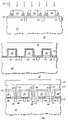
- FIG. 1Illustrated in FIG. 1 is a storage device structure 10 having a semiconductor substrate 12 , a silicon oxide layer 14 on semiconductor substrate 12 , and a plurality of patterned silicon nitride regions 16 on silicon oxide layer 14 .
- silicon oxide layer 14is 50–100 Angstroms thick, but it should be understood that various dimension geometries may be used and that semiconductor processing dimensions are continually shrinking.
- Patterned silicon nitride regions 16are, in one form, about 1000 Angstroms thick, about 1500 Angstroms wide, and about 1500 Angstroms apart. It should be understood that these dimensions are exemplary only and other dimensions, including much smaller dimensions, may be used. Additionally, these layers may run for a comparatively long length, for example the length of a memory array.
- Semiconductor substrate 12is preferably silicon but could be another semiconductor material, such as germanium, gallium arsenide, silicon on insulator (SOI) and other semiconductor materials.
- FIG. 2Illustrated in FIG. 2 is storage device structure 10 after formation of removable sidewall spacers 18 around patterned silicon nitride regions 16 .
- the formation of sidewall spacersis conventional and therefore will not be further detailed.
- removable sidewall spacers 18 in one formare deposited using a blanket deposition and etch but may also be formed by epitaxial growth.
- FIG. 3Illustrated in FIG. 3 is storage device structure 10 after an ion implant 20 to form doped regions 22 , 24 , and 26 between patterned silicon nitride regions 16 as masked by removable sidewall spacers 18 .
- Doped regions 22 , 24 , and 26are preferably doped to N-type to a depth for use as a source/drain.
- the N-type dopingcan be achieved using phosphorus or arsenic. It should be understood that other known doping chemistries may be used in lieu of either of these two materials.
- doped regions 22 , 24 , and 26can be doped to P-type instead of N-type.
- FIG. 4Illustrated in FIG. 4 is storage device structure 10 after removal of the removable sidewall spacers 18 has occurred. Additionally, the portion of silicon oxide layer 14 between the nitride layers is removed. This removal can be achieved in various conventional ways such as with a wet HF etch which is highly selective between nitride and oxide.
- a storage layer 28is formed comprising an atomic layer of nanoclusters or nanocrystals in a dielectric.
- Materials used for the nanocrystalsare silicon, silicon germanium, germanium and other semiconductor materials, including metal. It should be understood that the nanocrystals may not necessarily be crystalline in composition and thus this term is synonymous with nanoclusters which include non-crystalline materials.
- Various materialsmay be used in connection the storage layer 28 .
- storage layer 28may be implemented as a film of nitride that functions as discrete charge storing traps to store information. Other storage layer materials may also be used. It should also be understood that the thickness of the storage layer 28 may be several atoms in thickness or greater as opposed to a single atomic layer thickness. Additionally, the storage layer 28 may not necessarily be planar.
- gate layer 30Illustrated in FIG. 6 is storage device structure 10 after formation of a gate layer 30 .
- the gate layer 30is shown as a planar layer but it may also be formed as a conformal layer. Gate layer 30 may also be a stack of different conductive layers. Gate layer 30 is conductive. In one form the conductive characteristic is accomplished with a metal that is deposited by plating but could be another conductive material and could be deposited by another method for depositing a layer that can be useful as a gate. For example, gate layer 30 may be implemented as a layer of polysilicon. Various ways to form gate layer 30 exist such as deposition and plating techniques. In the case of plating, a seed layer (not separately shown) is formed before the plating of ultimate gate layer 30 . In one form the metal is tungsten but various metals and metal alloys may be used.
- FIG. 7Illustrated in FIG. 7 is storage device structure 10 after a planarizing process that removes gate layer 30 from over patterned silicon nitride regions 16 .
- the patterning of gate layer 30forms control gates 32 , 34 , 36 , and 38 between the patterned silicon nitride regions 16 .
- CMPchemical mechanical polishing
- Other planarizing techniquesmay be used. For example a timed etch process may be used as another etch back process.
- FIG. 8Illustrated in FIG. 8 is storage device structure 10 after removal of the patterned silicon nitride regions 16 and the underlying remaining portions of silicon oxide layer 14 .
- This removalis achieved by various removal processes.
- the patterned silicon nitride regions 16may be removed by using a dry chlorine etch which is commonly used for etching nitride. This dry etch also removes oxide but is selective to silicon.
- This etch processingleaves control gates 32 , 34 , 36 , and 38 and portions of semiconductor substrate 12 exposed.
- Another removal processsuch as a conventional chemical wet etch may be used.
- Under control gates 32 , 34 , 36 , and 38are storage layers 40 , 42 , 44 , and 46 , respectively, formed from storage layer 28 .
- FIG. 9Illustrated in FIG. 9 is storage device structure 10 after forming an insulating liner 47 on the exposed portions of semiconductor substrate 12 and control gates 32 , 34 , 36 , and 38 .
- insulating liner 47After the formation of insulating liner 47 , a plurality of conductive sidewall spacers or conductive spacers is formed adjacent and lateral to the control gates.
- conductive spacer 48is formed adjacent to control gate 32
- conductive spacers 49 and 50are formed adjacent to control gate 34
- conductive spacers 51 and 52are formed adjacent to control gate 36
- conductive spacer 53is formed adjacent to control gate 38 .
- Conductive spacers 48 , 49 , 50 , 51 , 52 and 53are conductive and are preferably formed of polysilicon. It should be understood that other conductive materials, such as metal, may be used.
- FIG. 10Illustrated in FIG. 10 is storage device structure 10 after an ion implant 56 forms doped regions 58 , 60 and 62 between control gates 32 , 34 , 36 , and 38 using conductive spacers 48 , 49 , 50 , 51 , 52 and 53 as a mask.
- This ion implantis preferably the same as ion implant 20 shown in FIG. 3 but other implant techniques may be used. For example, a different species of ions may be used to optimize the programming efficiency or improve electrical short channel effects associated with the doped regions 58 , 60 and 62 .
- the conductive spacers 48 , 49 , 50 , 51 , 52 and 53are permanent spacers as opposed to disposable spacers.
- the doped regions 58 , 60 and 62will function as either a drain or a source of the storage device structure 10 depending upon either the chosen conductivity of doped regions 58 , 60 and 62 or the voltage biasing of the doped regions 58 , 60 and 62 that is applied during operation.
- FIG. 11Illustrated in FIG. 11 is storage device structure 10 after formation of a blanket insulating or dielectric layer 113 .
- the dielectric layer 113is formed as a composite layer having a plurality of layers of insulative material. For example, multiple deposition steps are performed to result in a plurality of discrete insulating layers.
- the dielectric layer 113is etched to form contact vias in a conventional manner. Conductive contacts 93 , 95 and 97 are formed within the dielectric layer 113 to make direct electrical contact to the doped regions 58 , 60 and 62 .
- Overlying the dielectric layer 113is a conductive layer forming a row source line 81 .
- the conductive layer or strip of row source line 81is formed, in one form, as a blanket deposition and is then patterned to overlie the conductive contacts 93 , 95 and 97 and routed as necessary.
- the row source line 81is formed typically by deposition of a conductive material such as metal. It should be understood that any conductive material, such as polysilicon, may be used for row source line 81 .
- the storage device structure 10 of FIG. 11implements a plurality of memory cells that are positioned closely in an efficient manner.
- a first memory cellis formed of control gate 34 , a select gate from conductive spacer 50 , a drain from doped region 22 and a source from doped region 60 .
- An adjoining second memory cellis formed of control gate 34 , select gate formed by conductive spacer 49 , a drain from doped region 22 and a source from doped region 58 .
- Each control gateis associated with two memory cells. This structure enables a write or programming current of the memory cell to be reduced because of an enhanced vertical electron injection field that exists within the channel of the storage device structure 10 .
- electronsare directed into the storage layer 42 at the peripheral edge closest to an associated source. Because the electrons are immediately directed into the storage layer 42 as they move laterally from the source into the channel, the efficiency of charge transfer into the storage layer 42 is increased. As a result, as lower amount of programming is required to charge the storage layer 42 and enhanced operation is obtained. Further the close positioning of two memory cells with one control gate permits efficient scaling to smaller geometries. By using a buried diffusion region, such as the doped region 22 underlying the control gate 34 , efficient space utilization occurs.
- FIG. 12Illustrated in FIG. 12 is a top plan view of a virtual ground array area 80 containing the storage device structure 10 of FIG. 11 .
- Two row source lines 81 and 82are illustrated extending in parallel and overlying multiple memory cells.
- the row source lines 81 and 82are conductive and are typically metal. Intersecting and substantially perpendicular to the row source lines 81 and 82 are control gates 34 and 36 and drain formed by doped regions 22 and 24 .
- Row source line 81overlies the sources formed by doped regions 58 , 60 and 62 .
- row source line 82overlies the sources formed by doped regions 59 , 61 and 63 .
- a contact 93 to the source formed by doped region 58underlies the row source line 81 .
- a contact 95 to source diffusion 60underlies the row source line 81 .
- a conductive contact 97 to a source formed by a doped region 62underlies the row source line 81 .
- a contact 87 to a source formed by a doped region 59underlies the row source line 82 .
- a contact 89 to a source formed by a doped region 61underlies the row source line 82 .
- a contact 91 to a source formed by a doped region 63underlies the row source line 82 .
- a contact 83makes electrical contact to control gate 34 .
- a contact 85makes electrical contact to control gate 36 .
- Contacts 101 , 103 and 105respectively make electrical contact to the select gate of conductive spacer 49 , the drain at doped region 22 and the select gate formed by conductive spacer 50 .
- contacts 107 , 109 and 111respectively make electrical contact to the select gate formed by conductive spacer 51 , the drain at doped region 24 and the select gate formed by conductive spacer 52 .
- First and second doped regionsare formed within a substrate and on opposite sides of a region of sacrificial material.
- a discrete charge storage layeris formed overlying a substrate and between regions of the sacrificial material.
- a first conductive control electrode and a second conductive control electrodeoverlie the substrate and are on opposite sides of one of the regions of the sacrificial material.
- a first pair of select electrodesare formed along the two sides of the first conductive control electrode and a second pair of select electrodes are formed the two sides of the second conductive control electrode.
- a third doped regionis formed in the substrate between the first and second conductive control electrodes and functions as either a drain or a source, depending upon the conductivity type.
- the storage devices described hereinmay be implemented as various types of nonvolatile memory devices.
- One exemplary implementation of the storage devices taught hereinis as a Flash memory.
- a high density Flash memorymay be implemented.
- the high density Flash memorythat is realizable using the storage device described herein permits a compact source-side injection based memory. As a result, more bits of data may be stored in a same amount of area than conventional known memory structures.
- a method for forming a storage device structureA substrate of a first conductivity type is provided. Overlying regions of sacrificial material are formed. A first doped region of a second conductivity type opposite the first conductivity type and a second doped region of the second conductivity type is formed within the substrate and on opposite sides of one of the regions of sacrificial material. A discrete charge storage layer is formed overlying the substrate and between the regions of the sacrificial material. A first conductive control electrode and a second conductive control electrode are formed overlying the substrate and on opposite sides of the one of the regions of sacrificial material, the first and second conductive control electrodes each having a top surface and two sides.
- a first pair of select electrodesis formed along the two sides of the first conductive control electrode and a second pair of select electrodes is formed along the two sides of the second conductive control electrode.
- a third doped region of the second conductivity typeis formed in the substrate between the first and second conductive control electrodes.
- the first pair of select electrodesis formed by depositing a layer of polysilicon and anisotropically etching the layer of polysilicon to leave polysilicon sidewall spacers as the first pair of select electrodes.
- the third doped regionis formed by performing an implant using the polysilicon sidewall spacers as a mask.
- a metal layeris formed over the first and second conductive control electrodes and the third doped region.
- a contactis formed between the third doped region and the metal layer.
- nitrideis used as the sacrificial material.
- the discrete charge storage layer overlying the substrate between the sacrificial materialis formed by depositing a layer of nanoclusters and removing portions of the layer that are not underlying the first conductive control electrode and the second conductive control electrode.
- a method for forming a storage device structureincludes providing a semiconductor substrate, forming a first plurality of spaced apart doped regions in the substrate, and forming a plurality of spaced apart storage regions over the first plurality of doped regions, forming a plurality of spaced apart first electrodes over the plurality of storage regions.
- First sidewall spacersare formed on sidewalls of the plurality of spaced apart first electrodes, wherein the first sidewall spacers comprise one of a group consisting of a material that can be doped to become conductive and a material that is conductive.
- Dopantsare implanted using the first sidewall spacers as a mask to form a second plurality of spaced apart doped regions in the substrate.
- metal layersare formed over the second plurality of spaced apart doped regions. Contacts are formed between the metal layers and the second plurality of spaced apart doped regions.
- the plurality of spaced apart first electrodesare characterized as control gates and the first sidewall spacers are characterized as select gates.
- the first plurality of doped regionsis formed by forming spaced apart sacrificial layers over the substrate, wherein the spaced apart sacrificial layers have sidewalls. Second sidewall spacers are formed on the sidewalls of the sacrificial layers. An implant is made into the substrate using the sacrificial layers and the second sidewall spacers as a mask.
- the first sidewall spacersare formed by forming a conformal layer over the plurality of spaced apart first electrodes, wherein the conformal layer comprises one of the group consisting of a material that can be doped to become conductive and a material that is conductive.
- the conformal layeris anisotropically etched to leave the first sidewall spacers on the sidewalls of the plurality of spaced apart first electrodes.
- the conformal layeris characterized as comprising polysilicon.
- a storage device structureIn yet another form there is provided a storage device structure.
- a substrateis provided having a first doped region and a second doped region in the substrate.
- a first storage layeroverlies the first doped region.
- a second storage layeroverlies the second doped region.
- a first control gateis over the first storage layer and has a first sidewall and a second sidewall.
- a second control gateis over the second storage layer and has a first sidewall and a second sidewall.
- a first select gateis on the first sidewall of the first control gate and a second select gate is on the second sidewall of the first control gate.
- a third select gateis on the first sidewall of the second control gate.
- a fourth select gateis on the second sidewall of the second control gate.
- a third doped region in the substrateis between the second and third select gates.
- a metal layeroverlies the first and second control gates and the third doped region.
- a contactis between the third doped region and the metal layer.
- a dielectric layeris formed over the first and second control gates prior to forming the metal layer.
- a contact openingis formed through the dielectric layer to the third doped region.
- the first and second storage layersare formed of nanoclusters.
- the first, second, third, and fourth select gatesare polysilicon.
- the substrateis of a first conductivity type and the first, second, and third doped regions are of a second conductivity type.
- the third doped regionis substantially aligned to the second and third select gates.
- the third doped regionextends slightly under the second and third select gates.
- hot carrier injectioncan be also used in conjunction with the source side injection to cause programming at interior portions of the storage layer 42 at both a left side and a right side close to doped region 22 .
- HCIhot carrier injection
- SSIsingle bit of information
Landscapes
- Engineering & Computer Science (AREA)
- Chemical & Material Sciences (AREA)
- Nanotechnology (AREA)
- Physics & Mathematics (AREA)
- Mathematical Physics (AREA)
- Theoretical Computer Science (AREA)
- Crystallography & Structural Chemistry (AREA)
- Non-Volatile Memory (AREA)
Abstract
Description
- (1) “Source Side Injection Storage Device and Method Therefor”, Ser. No. 11/170,444 by Chindalore; and
- (2) “Source Side Injection Storage Device With Control Gates Adjacent To Shared Source/Drain and Method Therefor”, Ser. No. 11/170,446 by Hong et al.
Claims (6)
Priority Applications (4)
| Application Number | Priority Date | Filing Date | Title |
|---|---|---|---|
| US11/170,447US7132329B1 (en) | 2005-06-29 | 2005-06-29 | Source side injection storage device with spacer gates and method therefor |
| PCT/US2006/022281WO2007005191A1 (en) | 2005-06-29 | 2006-06-08 | Source side injection storage device with spacer gates and method therefor |
| US11/536,190US7550348B2 (en) | 2005-06-29 | 2006-09-28 | Source side injection storage device with spacer gates and method therefor |
| US11/536,099US7235823B2 (en) | 2005-06-29 | 2006-09-28 | Source side injection storage device with spacer gates and method therefor |
Applications Claiming Priority (1)
| Application Number | Priority Date | Filing Date | Title |
|---|---|---|---|
| US11/170,447US7132329B1 (en) | 2005-06-29 | 2005-06-29 | Source side injection storage device with spacer gates and method therefor |
Related Child Applications (2)
| Application Number | Title | Priority Date | Filing Date |
|---|---|---|---|
| US11/536,099DivisionUS7235823B2 (en) | 2005-06-29 | 2006-09-28 | Source side injection storage device with spacer gates and method therefor |
| US11/536,190DivisionUS7550348B2 (en) | 2005-06-29 | 2006-09-28 | Source side injection storage device with spacer gates and method therefor |
Publications (1)
| Publication Number | Publication Date |
|---|---|
| US7132329B1true US7132329B1 (en) | 2006-11-07 |
Family
ID=37301189
Family Applications (3)
| Application Number | Title | Priority Date | Filing Date |
|---|---|---|---|
| US11/170,447Expired - Fee RelatedUS7132329B1 (en) | 2005-06-29 | 2005-06-29 | Source side injection storage device with spacer gates and method therefor |
| US11/536,190Expired - Fee RelatedUS7550348B2 (en) | 2005-06-29 | 2006-09-28 | Source side injection storage device with spacer gates and method therefor |
| US11/536,099Expired - LifetimeUS7235823B2 (en) | 2005-06-29 | 2006-09-28 | Source side injection storage device with spacer gates and method therefor |
Family Applications After (2)
| Application Number | Title | Priority Date | Filing Date |
|---|---|---|---|
| US11/536,190Expired - Fee RelatedUS7550348B2 (en) | 2005-06-29 | 2006-09-28 | Source side injection storage device with spacer gates and method therefor |
| US11/536,099Expired - LifetimeUS7235823B2 (en) | 2005-06-29 | 2006-09-28 | Source side injection storage device with spacer gates and method therefor |
Country Status (2)
| Country | Link |
|---|---|
| US (3) | US7132329B1 (en) |
| WO (1) | WO2007005191A1 (en) |
Cited By (10)
| Publication number | Priority date | Publication date | Assignee | Title |
|---|---|---|---|---|
| US7253057B1 (en)* | 2006-04-06 | 2007-08-07 | Atmel Corporation | Memory cell with reduced size and standby current |
| US20080137417A1 (en)* | 2004-10-28 | 2008-06-12 | Bo-Young Seo | Semiconductor device having multi-bit nonvolatile memory cell and methods of fabricating the same |
| US20080157171A1 (en)* | 2006-12-29 | 2008-07-03 | Prashant Majhi | Dielectric barrier for nanocrystals |
| US7410910B2 (en) | 2005-08-31 | 2008-08-12 | Micron Technology, Inc. | Lanthanum aluminum oxynitride dielectric films |
| US20090111229A1 (en)* | 2007-10-31 | 2009-04-30 | Steimle Robert F | Method of forming a split gate non-volatile memory cell |
| US7560793B2 (en) | 2002-05-02 | 2009-07-14 | Micron Technology, Inc. | Atomic layer deposition and conversion |
| US7575978B2 (en)* | 2005-08-04 | 2009-08-18 | Micron Technology, Inc. | Method for making conductive nanoparticle charge storage element |
| US7927948B2 (en) | 2005-07-20 | 2011-04-19 | Micron Technology, Inc. | Devices with nanocrystals and methods of formation |
| US8367506B2 (en) | 2007-06-04 | 2013-02-05 | Micron Technology, Inc. | High-k dielectrics with gold nano-particles |
| US20140273478A1 (en)* | 2013-03-12 | 2014-09-18 | Taiwan Semiconductor Manufacturing Company, Ltd. | Reducing Defects in Patterning Processes |
Families Citing this family (7)
| Publication number | Priority date | Publication date | Assignee | Title |
|---|---|---|---|---|
| US8320191B2 (en) | 2007-08-30 | 2012-11-27 | Infineon Technologies Ag | Memory cell arrangement, method for controlling a memory cell, memory array and electronic device |
| US7961506B2 (en)* | 2008-02-05 | 2011-06-14 | Micron Technology, Inc. | Multiple memory cells with rectifying device |
| JP2010050208A (en)* | 2008-08-20 | 2010-03-04 | Renesas Technology Corp | Semiconductor device |
| US8951892B2 (en) | 2012-06-29 | 2015-02-10 | Freescale Semiconductor, Inc. | Applications for nanopillar structures |
| US8853027B2 (en) | 2012-10-01 | 2014-10-07 | Freescale Semiconductor, Inc. | Split gate flash cell |
| US20140167136A1 (en)* | 2012-12-14 | 2014-06-19 | Spansion Llc | Charge Trapping Device with Improved Select Gate to Memory Gate Isoloation |
| US10501087B2 (en)* | 2012-12-19 | 2019-12-10 | Volvo Truck Corporation | Method and arrangement for determining the speed behaviour of a leading vehicle |
Citations (6)
| Publication number | Priority date | Publication date | Assignee | Title |
|---|---|---|---|---|
| US6133098A (en) | 1999-05-17 | 2000-10-17 | Halo Lsi Design & Device Technology, Inc. | Process for making and programming and operating a dual-bit multi-level ballistic flash memory |
| US6228695B1 (en)* | 1999-05-27 | 2001-05-08 | Taiwan Semiconductor Manufacturing Company | Method to fabricate split-gate with self-aligned source and self-aligned floating gate to control gate |
| US6400610B1 (en)* | 2000-07-05 | 2002-06-04 | Motorola, Inc. | Memory device including isolated storage elements that utilize hole conduction and method therefor |
| US6710287B2 (en)* | 2002-08-22 | 2004-03-23 | Fu Sheng Industrial Co., Ltd. | Laser engraving and coloring method for a golf club head |
| US20040121540A1 (en) | 2002-12-17 | 2004-06-24 | Chi-Hui Lin | Stacked gate flash memory device and method of fabricating the same |
| US7064030B2 (en)* | 2004-10-08 | 2006-06-20 | Freescale Semiconductor, Inc. | Method for forming a multi-bit non-volatile memory device |
Family Cites Families (18)
| Publication number | Priority date | Publication date | Assignee | Title |
|---|---|---|---|---|
| US5866934A (en)* | 1997-06-20 | 1999-02-02 | Advanced Micro Devices, Inc. | Parallel and series-coupled transistors having gate conductors formed on sidewall surfaces of a sacrificial structure |
| US6346725B1 (en)* | 1998-05-22 | 2002-02-12 | Winbond Electronics Corporation | Contact-less array of fully self-aligned, triple polysilicon, source-side injection, nonvolatile memory cells with metal-overlaid wordlines |
| US6160287A (en)* | 1998-12-08 | 2000-12-12 | United Microelectronics Corp. | Flash memory |
| JP3201370B2 (en) | 1999-01-22 | 2001-08-20 | 日本電気株式会社 | Nonvolatile semiconductor memory device and method of manufacturing the same |
| JP4012341B2 (en) | 1999-07-14 | 2007-11-21 | 株式会社ルネサステクノロジ | Semiconductor integrated circuit device |
| US6901006B1 (en) | 1999-07-14 | 2005-05-31 | Hitachi, Ltd. | Semiconductor integrated circuit device including first, second and third gates |
| KR100821456B1 (en) | 2000-08-14 | 2008-04-11 | 샌디스크 쓰리디 엘엘씨 | Dense array and charge storage device and manufacturing method thereof |
| KR100437470B1 (en)* | 2001-01-31 | 2004-06-23 | 삼성전자주식회사 | Semiconductor device having a flash memory cell and fabrication method thereof |
| US6891262B2 (en) | 2001-07-19 | 2005-05-10 | Sony Corporation | Semiconductor device and method of producing the same |
| DE10153384B4 (en) | 2001-10-30 | 2007-08-02 | Infineon Technologies Ag | Semiconductor memory cell, method for its production and semiconductor memory device |
| EP2058275A1 (en) | 2003-01-07 | 2009-05-13 | Ramot at Tel-Aviv University Ltd. | Peptide nanostructures encapsulating a foreign material and method of manufacturing same |
| US6974739B2 (en)* | 2003-05-16 | 2005-12-13 | Promos Technologies Inc. | Fabrication of dielectric on a gate surface to insulate the gate from another element of an integrated circuit |
| KR100963768B1 (en)* | 2003-08-26 | 2010-06-14 | 엘지전자 주식회사 | Bag sealing device of refrigerator |
| US7042044B2 (en) | 2004-02-18 | 2006-05-09 | Koucheng Wu | Nor-type channel-program channel-erase contactless flash memory on SOI |
| US7020018B2 (en)* | 2004-04-22 | 2006-03-28 | Solid State System Co., Ltd. | Nonvolatile memory device and method for fabricating the same |
| US7518179B2 (en) | 2004-10-08 | 2009-04-14 | Freescale Semiconductor, Inc. | Virtual ground memory array and method therefor |
| US7183180B2 (en) | 2004-10-13 | 2007-02-27 | Atmel Corporation | Method for simultaneous fabrication of a nanocrystal and non-nanocrystal device |
| US7446371B2 (en) | 2004-10-21 | 2008-11-04 | Samsung Electronics Co., Ltd. | Non-volatile memory cell structure with charge trapping layers and method of fabricating the same |
- 2005
- 2005-06-29USUS11/170,447patent/US7132329B1/ennot_activeExpired - Fee Related
- 2006
- 2006-06-08WOPCT/US2006/022281patent/WO2007005191A1/enactiveApplication Filing
- 2006-09-28USUS11/536,190patent/US7550348B2/ennot_activeExpired - Fee Related
- 2006-09-28USUS11/536,099patent/US7235823B2/ennot_activeExpired - Lifetime
Patent Citations (6)
| Publication number | Priority date | Publication date | Assignee | Title |
|---|---|---|---|---|
| US6133098A (en) | 1999-05-17 | 2000-10-17 | Halo Lsi Design & Device Technology, Inc. | Process for making and programming and operating a dual-bit multi-level ballistic flash memory |
| US6228695B1 (en)* | 1999-05-27 | 2001-05-08 | Taiwan Semiconductor Manufacturing Company | Method to fabricate split-gate with self-aligned source and self-aligned floating gate to control gate |
| US6400610B1 (en)* | 2000-07-05 | 2002-06-04 | Motorola, Inc. | Memory device including isolated storage elements that utilize hole conduction and method therefor |
| US6710287B2 (en)* | 2002-08-22 | 2004-03-23 | Fu Sheng Industrial Co., Ltd. | Laser engraving and coloring method for a golf club head |
| US20040121540A1 (en) | 2002-12-17 | 2004-06-24 | Chi-Hui Lin | Stacked gate flash memory device and method of fabricating the same |
| US7064030B2 (en)* | 2004-10-08 | 2006-06-20 | Freescale Semiconductor, Inc. | Method for forming a multi-bit non-volatile memory device |
Cited By (22)
| Publication number | Priority date | Publication date | Assignee | Title |
|---|---|---|---|---|
| US7560793B2 (en) | 2002-05-02 | 2009-07-14 | Micron Technology, Inc. | Atomic layer deposition and conversion |
| US7589029B2 (en) | 2002-05-02 | 2009-09-15 | Micron Technology, Inc. | Atomic layer deposition and conversion |
| US20080137417A1 (en)* | 2004-10-28 | 2008-06-12 | Bo-Young Seo | Semiconductor device having multi-bit nonvolatile memory cell and methods of fabricating the same |
| US7521750B2 (en)* | 2004-10-28 | 2009-04-21 | Samsung Electronics Co., Ltd. | Semiconductor device having multi-bit nonvolatile memory cell and methods of fabricating the same |
| US8501563B2 (en) | 2005-07-20 | 2013-08-06 | Micron Technology, Inc. | Devices with nanocrystals and methods of formation |
| US8288818B2 (en) | 2005-07-20 | 2012-10-16 | Micron Technology, Inc. | Devices with nanocrystals and methods of formation |
| US8921914B2 (en) | 2005-07-20 | 2014-12-30 | Micron Technology, Inc. | Devices with nanocrystals and methods of formation |
| US7927948B2 (en) | 2005-07-20 | 2011-04-19 | Micron Technology, Inc. | Devices with nanocrystals and methods of formation |
| US9496355B2 (en) | 2005-08-04 | 2016-11-15 | Micron Technology, Inc. | Conductive nanoparticles |
| US7575978B2 (en)* | 2005-08-04 | 2009-08-18 | Micron Technology, Inc. | Method for making conductive nanoparticle charge storage element |
| US7410910B2 (en) | 2005-08-31 | 2008-08-12 | Micron Technology, Inc. | Lanthanum aluminum oxynitride dielectric films |
| US7531869B2 (en) | 2005-08-31 | 2009-05-12 | Micron Technology, Inc. | Lanthanum aluminum oxynitride dielectric films |
| US7253057B1 (en)* | 2006-04-06 | 2007-08-07 | Atmel Corporation | Memory cell with reduced size and standby current |
| US7763511B2 (en) | 2006-12-29 | 2010-07-27 | Intel Corporation | Dielectric barrier for nanocrystals |
| US20080157171A1 (en)* | 2006-12-29 | 2008-07-03 | Prashant Majhi | Dielectric barrier for nanocrystals |
| US8367506B2 (en) | 2007-06-04 | 2013-02-05 | Micron Technology, Inc. | High-k dielectrics with gold nano-particles |
| US9064866B2 (en) | 2007-06-04 | 2015-06-23 | Micro Technology, Inc. | High-k dielectrics with gold nano-particles |
| US7838363B2 (en)* | 2007-10-31 | 2010-11-23 | Freescale Semiconductor, Inc. | Method of forming a split gate non-volatile memory cell |
| US20090111229A1 (en)* | 2007-10-31 | 2009-04-30 | Steimle Robert F | Method of forming a split gate non-volatile memory cell |
| US20140273478A1 (en)* | 2013-03-12 | 2014-09-18 | Taiwan Semiconductor Manufacturing Company, Ltd. | Reducing Defects in Patterning Processes |
| US9123662B2 (en)* | 2013-03-12 | 2015-09-01 | Taiwan Semiconductor Manufacturing Company, Ltd. | Reducing defects in patterning processes |
| US9543160B2 (en)* | 2013-03-12 | 2017-01-10 | Taiwan Semiconductor Manufacturing Company, Ltd. | Reducing defects in patterning processes |
Also Published As
| Publication number | Publication date |
|---|---|
| US7235823B2 (en) | 2007-06-26 |
| WO2007005191A1 (en) | 2007-01-11 |
| US7550348B2 (en) | 2009-06-23 |
| US20070054452A1 (en) | 2007-03-08 |
| US20070020849A1 (en) | 2007-01-25 |
Similar Documents
| Publication | Publication Date | Title |
|---|---|---|
| US7235823B2 (en) | Source side injection storage device with spacer gates and method therefor | |
| US11069696B2 (en) | Device structure for a 3-dimensional NOR memory array and methods for improved erase operations applied thereto | |
| EP1923909B1 (en) | Charge trapping memory device and manufacturing method thereof | |
| US20200185394A1 (en) | Semiconductor device and manufacturing method thereof | |
| US8513727B2 (en) | Surrounding stacked gate multi-gate FET structure nonvolatile memory device | |
| US7652322B2 (en) | Split gate flash memory device having self-aligned control gate and method of manufacturing the same | |
| KR101552448B1 (en) | A non-volatile memory cell having a high k dielectric and metal gate | |
| US7268042B2 (en) | Nonvolatile semiconductor memory and making method thereof | |
| JP5806439B2 (en) | Memory cell and manufacturing method thereof | |
| US9231115B2 (en) | Semiconductor device and manufacturing method thereof | |
| CN101578706B (en) | Method of making a non-volatile memory device | |
| US11183510B2 (en) | Manufacturing method of semiconductor device and semiconductor device | |
| CN101174652B (en) | Self-aligned method and a memory array made thereby | |
| US20060249779A1 (en) | Multi-bit multi-level non-volatile memory device and methods of operating and fabricating the same | |
| US6287917B1 (en) | Process for fabricating an MNOS flash memory device | |
| JPH07123143B2 (en) | Non-volatile memory manufacturing method | |
| JP2007281092A (en) | Semiconductor device and manufacturing method thereof | |
| JP2007517386A (en) | BRIDGE FIELD EFFECT TRANSISTOR MEMORY CELL, DEVICE HAVING THE CELL, AND METHOD FOR MANUFACTURING BRIDGE FIELD EFFECT TRANSISTOR MEMORY CELL | |
| KR100608507B1 (en) | Method of manufacturing NRM memory cell array | |
| TWI390674B (en) | Source side injection storage device having control gate adjacent to shared source/drain and method thereof | |
| US7498222B1 (en) | Enhanced etching of a high dielectric constant layer | |
| US7064378B2 (en) | Local-length nitride SONOS device having self-aligned ONO structure and method of manufacturing the same | |
| US7355236B2 (en) | Non-volatile floating gate memory cells with polysilicon storage dots and fabrication methods thereof | |
| JP2007506275A (en) | Method of manufacturing non-volatile memory device and memory device obtained thereby | |
| US20060054963A1 (en) | Non-volatile and non-uniform trapped-charge memory cell structure and method of fabrication |
Legal Events
| Date | Code | Title | Description |
|---|---|---|---|
| AS | Assignment | Owner name:FREESCALE SEMICONDUCTOR, INC., TEXAS Free format text:ASSIGNMENT OF ASSIGNORS INTEREST;ASSIGNORS:HONG, CHEONG M.;CHINDALORE, GOWRISHANKAR L.;REEL/FRAME:016749/0690 Effective date:20050629 | |
| AS | Assignment | Owner name:CITIBANK, N.A. AS COLLATERAL AGENT, NEW YORK Free format text:SECURITY AGREEMENT;ASSIGNORS:FREESCALE SEMICONDUCTOR, INC.;FREESCALE ACQUISITION CORPORATION;FREESCALE ACQUISITION HOLDINGS CORP.;AND OTHERS;REEL/FRAME:018855/0129 Effective date:20061201 Owner name:CITIBANK, N.A. AS COLLATERAL AGENT,NEW YORK Free format text:SECURITY AGREEMENT;ASSIGNORS:FREESCALE SEMICONDUCTOR, INC.;FREESCALE ACQUISITION CORPORATION;FREESCALE ACQUISITION HOLDINGS CORP.;AND OTHERS;REEL/FRAME:018855/0129 Effective date:20061201 Owner name:CITIBANK, N.A. AS COLLATERAL AGENT, NEW YORK Free format text:SECURITY AGREEMENT;ASSIGNORS:FREESCALE SEMICONDUCTOR, INC.;FREESCALE ACQUISITION CORPORATION;FREESCALE ACQUISITION HOLDINGS CORP.;AND OTHERS;REEL/FRAME:018855/0129D Effective date:20061201 | |
| FPAY | Fee payment | Year of fee payment:4 | |
| AS | Assignment | Owner name:CITIBANK, N.A., AS COLLATERAL AGENT,NEW YORK Free format text:SECURITY AGREEMENT;ASSIGNOR:FREESCALE SEMICONDUCTOR, INC.;REEL/FRAME:024397/0001 Effective date:20100413 Owner name:CITIBANK, N.A., AS COLLATERAL AGENT, NEW YORK Free format text:SECURITY AGREEMENT;ASSIGNOR:FREESCALE SEMICONDUCTOR, INC.;REEL/FRAME:024397/0001 Effective date:20100413 | |
| AS | Assignment | Owner name:CITIBANK, N.A., AS NOTES COLLATERAL AGENT, NEW YORK Free format text:SECURITY AGREEMENT;ASSIGNOR:FREESCALE SEMICONDUCTOR, INC.;REEL/FRAME:030633/0424 Effective date:20130521 Owner name:CITIBANK, N.A., AS NOTES COLLATERAL AGENT, NEW YOR Free format text:SECURITY AGREEMENT;ASSIGNOR:FREESCALE SEMICONDUCTOR, INC.;REEL/FRAME:030633/0424 Effective date:20130521 | |
| AS | Assignment | Owner name:CITIBANK, N.A., AS NOTES COLLATERAL AGENT, NEW YORK Free format text:SECURITY AGREEMENT;ASSIGNOR:FREESCALE SEMICONDUCTOR, INC.;REEL/FRAME:031591/0266 Effective date:20131101 Owner name:CITIBANK, N.A., AS NOTES COLLATERAL AGENT, NEW YOR Free format text:SECURITY AGREEMENT;ASSIGNOR:FREESCALE SEMICONDUCTOR, INC.;REEL/FRAME:031591/0266 Effective date:20131101 | |
| FPAY | Fee payment | Year of fee payment:8 | |
| AS | Assignment | Owner name:FREESCALE SEMICONDUCTOR, INC., TEXAS Free format text:PATENT RELEASE;ASSIGNOR:CITIBANK, N.A., AS COLLATERAL AGENT;REEL/FRAME:037354/0225 Effective date:20151207 Owner name:FREESCALE SEMICONDUCTOR, INC., TEXAS Free format text:PATENT RELEASE;ASSIGNOR:CITIBANK, N.A., AS COLLATERAL AGENT;REEL/FRAME:037356/0143 Effective date:20151207 Owner name:FREESCALE SEMICONDUCTOR, INC., TEXAS Free format text:PATENT RELEASE;ASSIGNOR:CITIBANK, N.A., AS COLLATERAL AGENT;REEL/FRAME:037356/0553 Effective date:20151207 | |
| AS | Assignment | Owner name:MORGAN STANLEY SENIOR FUNDING, INC., MARYLAND Free format text:ASSIGNMENT AND ASSUMPTION OF SECURITY INTEREST IN PATENTS;ASSIGNOR:CITIBANK, N.A.;REEL/FRAME:037486/0517 Effective date:20151207 | |
| AS | Assignment | Owner name:MORGAN STANLEY SENIOR FUNDING, INC., MARYLAND Free format text:ASSIGNMENT AND ASSUMPTION OF SECURITY INTEREST IN PATENTS;ASSIGNOR:CITIBANK, N.A.;REEL/FRAME:037518/0292 Effective date:20151207 | |
| AS | Assignment | Owner name:NORTH STAR INNOVATIONS INC., CALIFORNIA Free format text:ASSIGNMENT OF ASSIGNORS INTEREST;ASSIGNOR:FREESCALE SEMICONDUCTOR, INC.;REEL/FRAME:037694/0264 Effective date:20151002 | |
| AS | Assignment | Owner name:NXP, B.V., F/K/A FREESCALE SEMICONDUCTOR, INC., NETHERLANDS Free format text:RELEASE BY SECURED PARTY;ASSIGNOR:MORGAN STANLEY SENIOR FUNDING, INC.;REEL/FRAME:040925/0001 Effective date:20160912 Owner name:NXP, B.V., F/K/A FREESCALE SEMICONDUCTOR, INC., NE Free format text:RELEASE BY SECURED PARTY;ASSIGNOR:MORGAN STANLEY SENIOR FUNDING, INC.;REEL/FRAME:040925/0001 Effective date:20160912 | |
| AS | Assignment | Owner name:NXP B.V., NETHERLANDS Free format text:RELEASE BY SECURED PARTY;ASSIGNOR:MORGAN STANLEY SENIOR FUNDING, INC.;REEL/FRAME:040928/0001 Effective date:20160622 | |
| AS | Assignment | Owner name:MORGAN STANLEY SENIOR FUNDING, INC., MARYLAND Free format text:CORRECTIVE ASSIGNMENT TO CORRECT THE REMOVE PATENTS 8108266 AND 8062324 AND REPLACE THEM WITH 6108266 AND 8060324 PREVIOUSLY RECORDED ON REEL 037518 FRAME 0292. ASSIGNOR(S) HEREBY CONFIRMS THE ASSIGNMENT AND ASSUMPTION OF SECURITY INTEREST IN PATENTS;ASSIGNOR:CITIBANK, N.A.;REEL/FRAME:041703/0536 Effective date:20151207 | |
| FEPP | Fee payment procedure | Free format text:MAINTENANCE FEE REMINDER MAILED (ORIGINAL EVENT CODE: REM.) | |
| LAPS | Lapse for failure to pay maintenance fees | Free format text:PATENT EXPIRED FOR FAILURE TO PAY MAINTENANCE FEES (ORIGINAL EVENT CODE: EXP.); ENTITY STATUS OF PATENT OWNER: LARGE ENTITY | |
| STCH | Information on status: patent discontinuation | Free format text:PATENT EXPIRED DUE TO NONPAYMENT OF MAINTENANCE FEES UNDER 37 CFR 1.362 | |
| FP | Lapsed due to failure to pay maintenance fee | Effective date:20181107 | |
| AS | Assignment | Owner name:SHENZHEN XINGUODU TECHNOLOGY CO., LTD., CHINA Free format text:CORRECTIVE ASSIGNMENT TO CORRECT THE TO CORRECT THE APPLICATION NO. FROM 13,883,290 TO 13,833,290 PREVIOUSLY RECORDED ON REEL 041703 FRAME 0536. ASSIGNOR(S) HEREBY CONFIRMS THE THE ASSIGNMENT AND ASSUMPTION OF SECURITYINTEREST IN PATENTS.;ASSIGNOR:MORGAN STANLEY SENIOR FUNDING, INC.;REEL/FRAME:048734/0001 Effective date:20190217 | |
| AS | Assignment | Owner name:MORGAN STANLEY SENIOR FUNDING, INC., MARYLAND Free format text:CORRECTIVE ASSIGNMENT TO CORRECT THE REMOVE APPLICATION11759915 AND REPLACE IT WITH APPLICATION 11759935 PREVIOUSLY RECORDED ON REEL 037486 FRAME 0517. ASSIGNOR(S) HEREBY CONFIRMS THE ASSIGNMENT AND ASSUMPTION OF SECURITYINTEREST IN PATENTS;ASSIGNOR:CITIBANK, N.A.;REEL/FRAME:053547/0421 Effective date:20151207 | |
| AS | Assignment | Owner name:NXP B.V., NETHERLANDS Free format text:CORRECTIVE ASSIGNMENT TO CORRECT THE REMOVEAPPLICATION 11759915 AND REPLACE IT WITH APPLICATION11759935 PREVIOUSLY RECORDED ON REEL 040928 FRAME 0001. ASSIGNOR(S) HEREBY CONFIRMS THE RELEASE OF SECURITYINTEREST;ASSIGNOR:MORGAN STANLEY SENIOR FUNDING, INC.;REEL/FRAME:052915/0001 Effective date:20160622 | |
| AS | Assignment | Owner name:NXP, B.V. F/K/A FREESCALE SEMICONDUCTOR, INC., NETHERLANDS Free format text:CORRECTIVE ASSIGNMENT TO CORRECT THE REMOVEAPPLICATION 11759915 AND REPLACE IT WITH APPLICATION11759935 PREVIOUSLY RECORDED ON REEL 040925 FRAME 0001. ASSIGNOR(S) HEREBY CONFIRMS THE RELEASE OF SECURITYINTEREST;ASSIGNOR:MORGAN STANLEY SENIOR FUNDING, INC.;REEL/FRAME:052917/0001 Effective date:20160912 |